

Page 1
UM2650
User manual
The STUSB4500 software programming guide
Introduction
This software guide is a non-exhaustive document aimed at clarifying a good practice when the customized STUSB4500
software is being written.
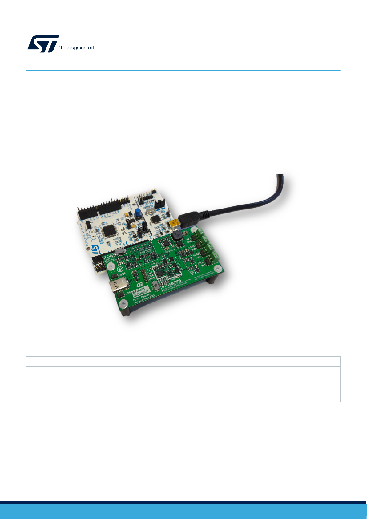
Figure 1. STEVAL-ISC005V1
Table 1. Minimal configuration
1 x NUCLEO-F072RB STM32 Nucleo-64 development board with ARM Cortex M0
1 x STEVAL-ISC005V1 STUSB4500 evaluation board
STSW-STUSB003
IAR 8.x C code compiler
UM2650 - Rev 2 - December 2020
For further information contact your local STMicroelectronics sales office.
Software library including STUSB4500 hardware abstraction layers, drivers and
code example
www
.st.com
Page 2
1 How to?
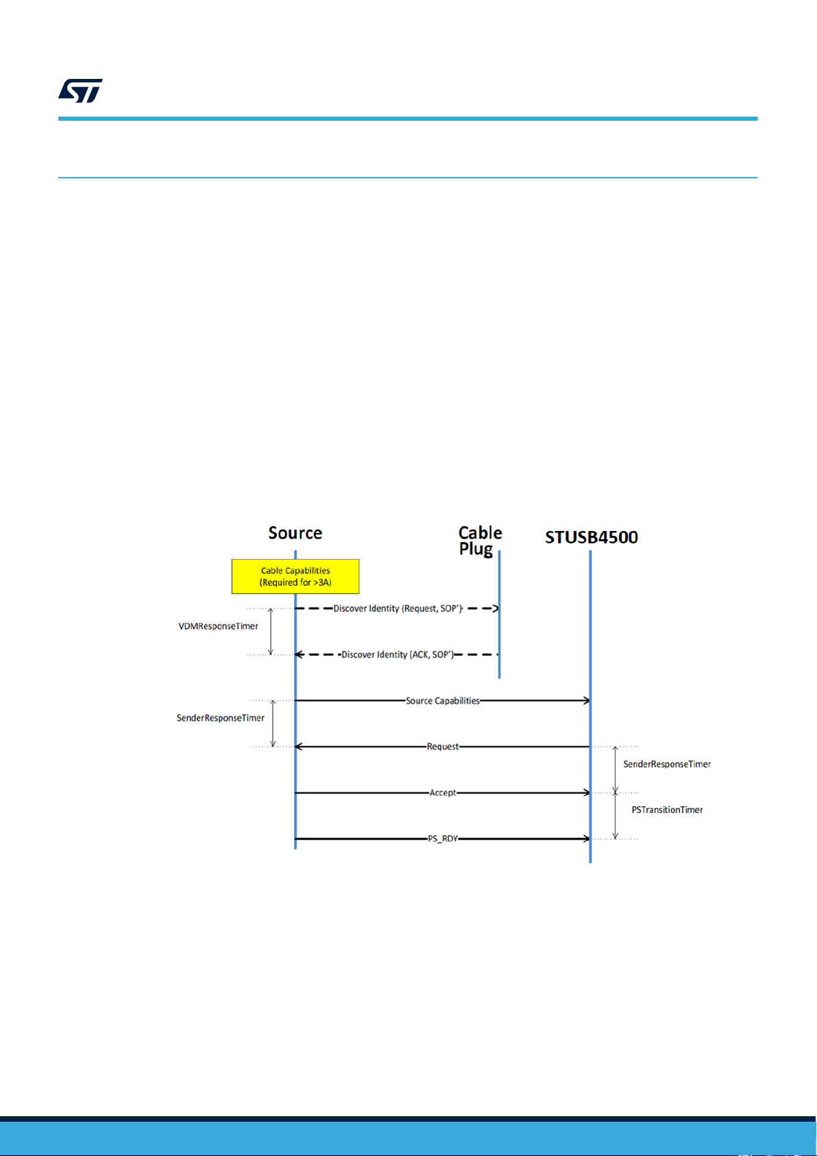
1.1 How USB PD negotiation works
1. At connection, a source connects to a sink @ 5 V (Type-C), therefore first of all, the STUSB4500 advertises
itself as a USB T
Then, a USB PD capable source advertises its power budget (SRC_PDOj) to the STUSB4500.
2.
3. The sink (STUSB4500) is responsible for:
a. evaluating the SRC_PDOj according to application needs (stored in STUSB4500 SNK_PDOi) thanks to
an internal algorithm
b. sending a request (voltage, current) to the SOURCE if any of the SRC_PDOj is compatible with any
SNK_PDOi (power MATCH). In case of failure, the negotiation ends with a USB PD mismatch.
4. The SOURCE is responsible for:
a. accepting or declining the request (RDO) sent by the STUSB4500.
b. if accepted, implementing the voltage and current transition from current profile to the new power
profile (within 275 ms after "accept")
c. notifying the SINK about the transition to new power profile is completed (PS_READY)
ype-C SINK.
UM2650
How to?
Figure 2. USB PD negotiation
1.2 How to initialize the STUSB4500 properly
In order to properly initialize the STUSB4500 for software operations, it is recommended to:
1. Clear all interrupts by reading (I²C multi-read command for instance) all 10 registers from address 0x0D to
0x16
2.
Configure interrupt mask register (@0x0C) according to application requirements (recommended list of
alerts to be unmasked: CONNECTION_STATUS, MONITORING_STATUS, PRT_STATUS)
For further details, see the STSW-STUSB003 function: usb_pd_init
UM2650 - Rev 2
page 2/49
Page 3
1.3 How to send a USB PD software reset
In order to send a USB PD “SOFT_RESET_MESSAGE” command, the following sequence must be done:
1. WRITE 0x0D (SOFT_RESET) in the TX_HEADER_LOW register (@0x51)
2.
WRITE 0x26 (SEND_COMMAND) in the PD_COMMAND_CTRL register (@ 0x1A)
For further details, see STSW-STUSB003 function Send_Soft_reset_Message
1.4 How to fill the PDO registers
The STUSB4500 supports up to 3 fixed supply PDO. As per USB PD standard, a SINK PDO is composed 32 bits
that must be filled according to figure below
PDO1, PDO2 and PDO3 from the STUSB4500 can be changed by software by accessing respectively the
registers 0x85-0x88, 0x89-0x8C and 0x8D-0x90. Each PDO is composed of a word of 4 bytes. Please note PDO1
must be fixed 5 V according to USB PD standard.
Bits Description
B31...30 Fixed supply
B29 Dual-role power
B28 Higher capability
B27 Unconstrained power
B26 USB communication capable
B25 Dual-role data
B24..23
B22..20 Reserved-Shall be set to zero
B19...10 V
B9...0 Operational current in 10 mA units
.
able 2. Fixed supply PDO-sink
T
Fast role swap required USB-Type-C current:
- 00b: fast swap not supported (default)
- 01b: default USB power
- 10b: 1.5 A@5 V
- 1
1b: 3.0 A@5 V
oltage in 50 mV units
UM2650
How to send a USB PD software reset
Filling the PDO register only does not force new PDO contract negotiation. Please check Section 1.5 How to
force the STUSB4500 to re-negotiate with the SOURCE.
For further details, see STSW-STUSB003 function:
Update_PDO
1.5 How to force the STUSB4500 to re-negotiate with the SOURCE
As per USB PD standard, a new contract negotiation must occur when a SOFT_RESET_MESSAGE is sent (by
either the SOURCE or the SINK).
Therefore, once the PDO registers have been updated by software, sending a SOFT_RESET_MESSAGE to the
SOURCE a new USB PD negotiation starts, by taking into account the new STUSB4500 PDO values (please
check Section 1.3 How to send a USB PD software reset).
1.6 How to force VBUS to 5 V
An easy way to force the STUSB4500 to negotiate 5 V is to set the number of active PDO to 1 (cf register 0x70:
DPM_PDO_NUMB register) followed by a SOFT_RESET_MESSAGE (please check Section 1.3 How to send a
USB PD software reset).
For further details, see STSW-STUSB003 functions: Negotiate_5V
UM2650 - Rev 2
, Update_Valid_PDO_Number
page 3/49
Page 4
UM2650
How to read USB-C connection STATUS
1.7 How to read USB-C connection STATUS
By accessing the 2 registers below:
• POR
T_STATUS_1 (@0x0E)
• CC_STATUS (@0x11)
It is possible to report the following information to the application processor:
1. the plug orientation (CC pin attached to CC1 or CC2)
2. the USB-C source current (Rp resistor value)
Note: At the connection, the STUSB4500 connects first in USB-C mode before negotiating any USB PD contract. In
order to know the final connection status (USB-C or USB PD explicit contract), it is recommended to wait 500 ms
after ATTACH event.
For further details, see STSW-STUSB003 function: Print_Type_C_Only_Status
1.8 How to read USB PD STATUS
By accessing the 4 registers below:
•
RDO_REG_ST
• RDO_REG_STATUS_1 (@0x92)
• RDO_REG_STATUS_2 (@0x93)
• RDO_REG_STATUS_3 (@0x94)
it is possible to report to the application processor some information:
• if the STUSB4500 is attached in USB-C mode (object position = 000b) or in USB PD contract (object
position different from 000b)
• the PDO index from the SOURCE that has been requested by the STUSB4500 internal algorithm (if object
position is different from 000b)
• and various information as per USB PD standard definition (see table below)
ATUS_0 (@0x91)
Table 3. Fixed request data object RDO
Bits Description
B31 Reserved-Shall be set to zero
B30....28 Object position (000b is Reserved and
B27 GiveBack flag = 0
B26 Capability mismatch
B25 USB communications capable
B24 No USB suspend
B23 Unchunked extended messages supported
B22....20 Reserved-Shall
B19...10 Operating current in 10 mA units
B9..0 Maximum operating current 10 mA units
be set to zero
For further details, see STSW-STUSB003 function: Print_RDO;
1.9 How to access to the PDO from the SOURCE
As a normal process from the USB-PD negotiation (see Section 1.1 How USB PD negotiation works),
the SOURCE initiates a USB PD contract negotiation by sharing its POWER profile (SRC_PDO) with the
STUSB4500.
It is possible to access these power profiles at the beginning of the power negotiation by reading the RX_Buffer
after confirmation from PR
T_STATUS register. This dynamic register flags each incoming message.
Shall Not be used)
UM2650 - Rev 2
page 4/49
Page 5

How to access the STUSB4500 policy engine state
When an incoming message is reported, its content is temporarily stored in the RX buffers (from 0x31 to 0x4E).
As each incoming message overrides the former message, it is important to quickly store in application processor
memory the STUSB4500 RX buffer content (header + data object) in order to catch the SOURCE power profiles.
For further details, see STSW
-STUSB003 functions: ALARM_MANAGEMENT, Print_PDO_FROM_SRC
1.10 How to access the STUSB4500 policy engine state
In order to understand what is the current state of the USB PD negotiation, it is possible to monitor in real time
the STUSB4500 policy engine FSM. Please refer to PE_FSM register (@0x29) or check Get_Device_STA
function from the STSW-STUSB003 library.
UM2650
TUS
UM2650 - Rev 2
page 5/49
Page 6

2 Register map
Offset Register name Description
0x06 BCD_TYPEC_REV_LOW BCD_TYPEC_REV_LOW register
0x07 BCD_TYPEC_REV_HIGH BCD_TYPEC_REV_HIGH register
0x08 BCD_USBPD_REV_LOW BCD_USBPD_REV_LOW register
0x09 BCD_USBPD_REV_HIGH BCD_USBPD_REV_HIGH register
0x0A DEVICE_CAPAB_HIGH DEVICE_CAPAB_HIGH register
0x0B ALERT_STATUS_1 ALERT_STATUS_1 register
0x0C ALERT_STATUS_1_MASK ALERT_STATUS_1_MASK register
0x0D PORT_STATUS_0 PORT_STATUS_0 register
0x0E PORT_STATUS_1 PORT_STATUS_1 register
0x0F TYPEC_MONITORING_STATUS_0 TYPEC_MONITORING_STATUS_0 register
0x10 TYPEC_MONITORING_STATUS_1 TYPEC_MONITORING_STATUS_1 register
0x11 CC_STATUS CC_STATUS register
0x12 CC_HW_FAULT_STATUS_0 CC_HW_FAULT_STATUS_0 register
0x13 CC_HW_FAULT_STATUS_1 CC_HW_FAULT_STATUS_1 register
0x14 PD_TYPEC_STATUS PD_TYPEC_STATUS register
0x15 TYPEC_STATUS TYPEC_STATUS register
0x16 PRT_STATUS PRT_STATUS register
0x17
to
Reserved Reserved
0x19
0x1A PD_COMMAND_CTRL PD_COMMAND_CTRL register
0x1B
to
reserved reserved
0x1F
0x20 MONITORING_CTRL_0 MONITORING_CTRL_0 register
0x21 Reserved Reserved
0x22 MONITORING_CTRL_2 MONITORING_CTRL_2 register
0x23 RESET_CTRL RESET_CTRL register
0x24 Reserved Reserved
0x25 VBUS_DISCHARGE_TIME_CTRL VBUS_DISCHARGE_TIME_CTRL register
0x26 VBUS_DISCHARGE_CTRL VBUS_DISCHARGE_CTRL register
0x27 VBUS_CTRL VBUS_CTRL register
0x28 reserved Reserved
0x29 PE_FSM PE_FSM register
0x2B reserved reserved
0x2C reserved reserved
0x2D GPIO_SW_GPIO GPIO_SW_GPIO register
UM2650
Register map
Table 4. Register map
UM2650 - Rev 2
page 6/49
Page 7

Offset Register name Description
0x2E reserved reserved
0x2F Device_ID Device_ID register
0x30 reserved reserved
0x31 RX_HEADER_LOW RX_HEADER_LOW register
0x32 RX_HEADER_HIGH RX_HEADER_HIGH register
0x33 RX_DATA_OBJ1_0 RX_DATA_OBJ1_0 register
0x34 RX_DATA_OBJ1_1 RX_DATA_OBJ1_1 register
0x35 RX_DATA_OBJ1_2 RX_DATA_OBJ1_2 register
0x36 RX_DATA_OBJ1_3 RX_DATA_OBJ1_3 register
0x37 RX_DATA_OBJ2_0 RX_DATA_OBJ2_0 register
0x38 RX_DATA_OBJ2_1 RX_DATA_OBJ2_1 register
0x39 RX_DATA_OBJ2_2 RX_DATA_OBJ2_2 register
0x3A RX_DATA_OBJ2_3 RX_DATA_OBJ2_3 register
0x3B RX_DATA_OBJ3_0 RX_DATA_OBJ3_0 register
0x3C RX_DATA_OBJ3_1 RX_DATA_OBJ3_1 register
0x3D RX_DATA_OBJ3_2 RX_DATA_OBJ3_2 register
0x3E RX_DATA_OBJ3_3 RX_DATA_OBJ3_3 register
0x3F RX_DATA_OBJ4_0 RX_DATA_OBJ4_0 register
0x40 RX_DATA_OBJ4_1 RX_DATA_OBJ4_1 register
0x41 RX_DATA_OBJ4_2 RX_DATA_OBJ4_2 register
0x42 RX_DATA_OBJ4_3 RX_DATA_OBJ4_3 register
0x43 RX_DATA_OBJ5_0 RX_DATA_OBJ5_0 register
0x44 RX_DATA_OBJ5_1 RX_DATA_OBJ5_1 register
0x45 RX_DATA_OBJ5_2 RX_DATA_OBJ5_2 register
0x46 RX_DATA_OBJ5_3 RX_DATA_OBJ5_3 register
0x47 RX_DATA_OBJ6_0 RX_DATA_OBJ6_0 register
0x48 RX_DATA_OBJ6_1 RX_DATA_OBJ6_1 register
0x49 RX_DATA_OBJ6_2 RX_DATA_OBJ6_2 register
0x4A RX_DATA_OBJ6_3 RX_DATA_OBJ6_3 register
0x4B RX_DATA_OBJ7_0 RX_DATA_OBJ7_0 register
0x4C RX_DATA_OBJ7_1 RX_DATA_OBJ7_1 register
0x4D RX_DATA_OBJ7_2 RX_DATA_OBJ7_2 register
0x4E RX_DATA_OBJ7_3 RX_DATA_OBJ7_3 register
0x51 TX_HEADER_LOW TX_HEADER_LOW register
0x52 TX_HEADER_HIGH TX_HEADER_HIGH register
0x53
to
Reserved reserved
0x6F
0x70 DPM_PDO_NUMB DPM_PDO_NUMB register
0x71
reserved reserved
to
UM2650
Register map
UM2650 - Rev 2
page 7/49
Page 8

Offset Register name Description
0x84
0x85 DPM_SNK_PDO1_0 DPM_SNK_PDO1_0 register
0x86 DPM_SNK_PDO1_1 DPM_SNK_PDO1_1 register
0x87 DPM_SNK_PDO1_2 DPM_SNK_PDO1_2 register
0x88 DPM_SNK_PDO1_3 DPM_SNK_PDO1_3 register
0x89 DPM_SNK_PDO2_0 DPM_SNK_PDO2_0 register
0x8A DPM_SNK_PDO2_1 DPM_SNK_PDO2_1 register
0x8B DPM_SNK_PDO2_2 DPM_SNK_PDO2_2 register
0x8C DPM_SNK_PDO2_3 DPM_SNK_PDO2_3 register
0x8D DPM_SNK_PDO3_0 DPM_SNK_PDO3_0 register
0x8E DPM_SNK_PDO3_1 DPM_SNK_PDO3_1 register
0x8F DPM_SNK_PDO3_2 DPM_SNK_PDO3_2 register
0x90 DPM_SNK_PDO3_3 DPM_SNK_PDO3_3 register
0x91 RDO_REG_STATUS_0 RDO_REG_STATUS_0 register
0x92 RDO_REG_STATUS_1 RDO_REG_STATUS_1 register
0x93 RDO_REG_STATUS_2 RDO_REG_STATUS_2 register
0x94 RDO_REG_STATUS_3 RDO_REG_STATUS_3 register
UM2650
Register map
UM2650 - Rev 2
page 8/49
Page 9

3 Register description
3.1 BCD_TYPEC_REV_LOW register
7 6 5 4 3 2 1 0
Address: STUSB_BLOCKBaseAddress + 0x06
: R
Type
Reset: 0x12
UM2650
Register description
BCD_TYPEC_REV_7_0
R
[7:0] BCD_TYPEC_REV_7_0: Defined T
ype-C release supported by the device
3.2 BCD_USPD_REV_HIGH register
7 6 5 4 3 2 1 0
Address: STUSB_BLOCKBaseAddress + 0x09
Type
: R
Reset: 0x20
[7:0] BCD_USBPD_REV_15_8: Defined Power Delivery release supported by the device
BCD_USBPD_REV_15_8
R
UM2650 - Rev 2
page 9/49
Page 10

3.3 BCD_USBPD_REV_LOW register
7 6 5 4 3 2 1 0
Address: STUSB_BLOCKBaseAddress + 0x08
T
: R
ype
Reset: 0x11
[7:0] BCD_USBPD_REV_7_0: Defined Power Delivery release supported by the device
3.4 BCD_USPD_REV_HIGH register
UM2650
BCD_USBPD_REV_LOW register
BCD_USBPD_REV_7_0
R
7 6 5 4 3 2 1 0
Address: STUSB_BLOCKBaseAddress + 0x09
: R
Type
Reset: 0x20
[7:0] BCD_USBPD_REV_15_8: Defined Power Delivery release supported by the device
3.5 DEVICE_CAPAB_HIGH register
7 6 5 4 3 2 1 0
Address: STUSB_BLOCKBaseAddress + 0x0A
Type
: R
Reset: 0x00
BCD_USBPD_REV_15_8
R
DEVICE_CAPAB_HIGH
R
UM2650 - Rev 2
[7:0] DEVICE_CAPAB_HIGH: Not used
page 10/49
Page 11

3.6 ALERT_STATUS_1 register
7 6 5 4 3 2 1 0
UM2650
ALERT_STATUS_1 register
reserved
PORT_STATUS_AL
CC_HW_FAULT_STATUS_AL
TYPEC_MONITORING_STATUS_AL
R R R R R R R R
PD_TYPEC_STATUS_AL
reserved
Address: STUSB_BLOCKBaseAddress + 0x0B
T
: R
ype
Reset: 0x00
[7] reserved
[6] PORT_STATUS_AL
[5] TYPEC_MONITORING_STATUS_AL
[4] CC_HW_FAULT_STATUS_AL
[3] reserved
[1] PRT_STATUS_AL
[0] reserved
reserved
PRT_STATUS_AL
UM2650 - Rev 2
page 11/49
Page 12

3.7 ALERT_STATUS_1_MASK register
7 6 5 4 3 2 1 0
UM2650
ALERT_STATUS_1_MASK register
reserved
PORT_STATUS_AL_MASK
CC_FAULT_STATUS_AL_MASK
TYPEC_MONITORING_STATUS_MASK
R/W R/W R/W R/W R/W R R/W R/W
reserved
reserved
PRT_STATUS_AL_MASK
Address: STUSB_BLOCKBaseAddress + 0x0C
T
: R/W
ype
Reset: 0xFB (initialized by NVM)
[7] reserved
PORT_STATUS_AL_MASK
[6]
0: (UNMASKED) Interrupt unmasked
1: (MASKED) Interrupt masked
TYPEC_MONITORING_STATUS_MASK
[5]
0: (UNMASKED) Interrupt unmasked
1: (MASKED) Interrupt masked
CC_FAULT_STATUS_AL_MASK
[4]
0: (UNMASKED) Interrupt unmasked
1: (MASKED) Interrupt masked
[3] reserved
[2] reserved
PRT_STATUS_AL_MASK:
[1]
0: (UNMASKED) Interrupt unmasked
1: (MASKED) Interrupt masked
[0] reserved
reserved
UM2650 - Rev 2
page 12/49
Page 13

3.8 PORT_STATUS_0 register
7 6 5 4 3 2 1 0
UM2650
PORT_STATUS_0 register
Address: STUSB_BLOCKBaseAddress + 0x0D
T
: R
ype
Reset: 0x00
ATTACH_TRANS:
[0]
0: No transition detected in attached states
1: T
ransition detected in attached state
RESERVED
ATTACH_TRANS
R RC
UM2650 - Rev 2
page 13/49
Page 14

3.9 PORT_STATUS_1 register
7 6 5 4 3 2 1 0
ATTACHED_DEVICE reserved POWER_MODE DATA_MODE reserved ATTACH
R R R R R R
Address: STUSB_BLOCKBaseAddress + 0x0E
T
: R
ype
Reset: 0x00
ATTACHED_DEVICE:
000: (NONE_A
001: (SNK_A
[7:5]
[4] reserved
[3]
[2]
[1] reserved
[0]
010: reserved
011: (DBG_ATT) Debug accessory device connected
100: reserved
101: reserved
Others: Do not use
POWER_MODE:
0: device is sinking power
1: reserved
DATA_MODE:
0: UFP
1: reserved
ATTACH:
0: UNA
1: ATTACHED
TT) No device connected
TT) Sink device connected
ACHED
TT
UM2650
PORT_STATUS_1 register
UM2650 - Rev 2
page 14/49
Page 15

3.10 TYPEC_MONITORING_STATUS_0 register
7 6 5 4 3 2 1 0
UM2650
TYPEC_MONITORING_STATUS_0 register
RESERVED
VBUS_HIGH_STATUS
R RC RC RC RC RC R
VBUS_LOW_STATUS
VBUS_READY_TRANS
VBUS_VSAFE0V_TRANS
Address: STUSB_BLOCKBaseAddress + 0x0F
T
: RC
ype
Reset: 0x0F
VBUS_HIGH_STATUS: VBUS_HIGH status updated during VBUS_READY transition from HIGH to LOW
[5]
0: (VBUS_HIGH_OK) VBUS below high threshold
1: (VBUS_HIGH_KO) VBUS above high threshold (Overvoltage condition)
VBUS_LOW_STATUS: VBUS_LOW status updated during VBUS_READY transition from HIGH to LOW
[4]
0: (VBUS_LOW_OK) VBUS above low threshold
1: (VBUS_LOW_KO) VBUS below low threshold (Undervoltage condition)
VBUS_READY_TRANS:
[3]
0: (NO_TRANS) status cleared
1: (TRANS_DETECTED) T
VBUS_VSAFE0V_TRANS:
[2]
0: (NO_TRANS) status cleared
1: (TRANS_DETECTED) Transition detected on VBUS_VSAFE0V bit
VBUS_V
[1]
0: (NO_TRANS) status cleared
1: (TRANS_DETECTED) Transition detected on VBUS_V
[0] reserved
ALID_SNK_TRANS:
ransition detected on VBUS_READY bit
ALID_SNK bit
RESERVED
VBUS_VALID_SNK_TRANS
UM2650 - Rev 2
page 15/49
Page 16

3.11 TYPEC_MONITORING_STATUS_1 register
7 6 5 4 3 2 1 0
UM2650
TYPEC_MONITORING_STATUS_1 register
RESERVED
R R R R R
Address: STUSB_BLOCKBaseAddress + 0x10
T
: R
ype
Reset: 0x00
VBUS_READY:
[3]
0: (NO_VBUS_READY) VBUS disconnected (Unpowered or vSafe0V)
1: (VBUS_READY) VBUS connected (vSafe5V or negotiated power level)
VBUS_VSAFE0V:
[2]
0: (NO_VSAFE0V) VBUS is higher than 0.8 V
1: (VSAFE0V) VBUS is lower than 0.8 V
VBUS_VALID_SNK:
[1]
0: (NO_VBUS_V
1: (VBUS_V
[0] reserved
ALID_SNK) VBUS is lower than 1.9 V or 3.5 V (depending of VBUS_SNK_DISC_THRESHOLD value)
ALID_SNK) VBUS is higher than 1.9 V or 3.5 V (depending of VBUS_SNK_DISC_THRESHOLD value)
VBUS_READY
VBUS_VSAFE0V
RESERVED
VBUS_VALID_SNK
UM2650 - Rev 2
page 16/49
Page 17

3.12 CC_STATUS register
7 6 5 4 3 2 1 0
UM2650
CC_STATUS register
RESERVED
LOOKING_4_CONNECTION
R R R R R
Address: STUSB_BLOCKBaseAddress + 0x1
ype: R
T
CONNECT_RESULT
1
CC2_STATE
Reset: 0x00
LOOKING_4_CONNECTION:
0: (NOT_LOOKING) The device is not actively looking for a connection. A transition from '1' to '0' indicates a potential
[5]
connection has been found. When the device is in power-up sequence or when TYPE-C FSM is in the following states:
Attached.SNK, DebugAccessory
1: (LOOKING) The device is looking for a connection
CONNECT_RESUL
0: Reserved.
[4]
1: (PRESENT_RD) The device is presenting Rd. When when TYPE-C FSM is in the following states: Attached.SNK,
DebugAccessory.SNK
CC2_ST
ATE: (available when CONNECT_result =1)
00: Reserved
01: SNK.Default (Above minimum vRd-Connect)
[3:2]
10: SNK.Power1.5 (Above minimum vRd-Connect)
11: SNK.Power3.0 (Above minimum vRd-Connect)
This field returns 00b if (LOOKING_4_CONNECTION=1)
CC1_ST
ATE: (available when CONNECT_result =1)
00: Reserved
01: SNK.Default (Above minimum vRd-Connect)
[1:0]
10: SNK.Power1.5 (Above minimum vRd-Connect)
11: SNK.Power3.0 (Above minimum vRd-Connect)
This field returns 00b if (LOOKING_4_CONNECTION=1)
T:
.SNK
CC1_STATE
UM2650 - Rev 2
page 17/49
Page 18

3.13 CC_HW_FAULT_STATUS_0 register
7 6 5 4 3 2 1 0
UM2650
CC_HW_FAULT_STATUS_0 register
RESERVED
R R RC RC RC R R R
RESERVED
VPU_OVP_FAULT_TRANS
VPU_VALID_TRANS
RESERVED
RESERVED
Address: STUSB_BLOCKBaseAddress + 0x12
T
: R
ype
Reset: 0x10
[7] reserved
VPU_OVP_FAULT_TRANS:
[5]
0: (NO_TRANS) Cleared
1: (TRANS_DETECTED) T
VPU_VALID_TRANS:
[4]
0: (NO_TRANS) Cleared
1: (TRANS_DETECTED) Transition occurred on VPU_V
[3] reserved
[2] reserved
[1] reserved
[0] reserved
ransition occurred on VPU_OVP_FAULT bit
ALID bit
RESERVED
RESERVED
UM2650 - Rev 2
page 18/49
Page 19

3.14 CC_HW_FAULT_STATUS_1 register
7 6 5 4 3 2 1 0
UM2650
CC_HW_FAULT_STATUS_1 register
VPU_VALID
VPU_OVP_FAULT
R R R R R R R R
RESERVED
RESERVED
VBUS_DISCH_FAULT
RESERVED
RESERVED
Address: STUSB_BLOCKBaseAddress + 0x13
T
: R
ype
Reset: 0x40
VPU_OVP_FAULT:
0: (NO_F
[7]
threshold of 6.0 V)
1: (FAULT) Overvoltage condition has occurred on CC pins when in pull-up mode (CC pins voltage is above overvoltage
threshold of 6.0 V)
VPU_VALID:
[6]
0: (NO_VALID) CC pins pull-up voltage is below UVLO threshold of 2.8 V when in pull-up mode
1: (V
ALID) CC pins pull-up voltage is above UVLO threshold of 2.8 V when in pull-up mode (normal operating condition)
VBUS_DISCH_FAULT:
[4]
0: (NO_FAUL
1: (FAULT) VBUS discharge issue has occurred
[3] reserved
[2] reserved
[1] reserved
[0] reserved
T) No overvoltage condition on CC pins when in pull-up mode (CC pins voltage is below overvoltage
AUL
T) No VBUS discharge issue
RESERVED
UM2650 - Rev 2
page 19/49
Page 20

3.15 PD_TYPEC_STATUS register
7 6 5 4 3 2 1 0
RESERVED PD_TYPEC_HAND_CHECK
R RC
Address: STUSB_BLOCKBaseAddress + 0x14
T
: R
ype
Reset: 0x00
UM2650
PD_TYPEC_STATUS register
PD_TYPEC_HAND_CHECK: hand checking sent by T
0000: (CLEARED) cleared
0001: reserved
0010: reserved
1: reserved
001
0100: reserved
0101: reserved
0110: reserved
[3:0]
0111: reserved
1000: (PD_HARD_RESET_COMPLETE_ACK)
1001: reserved
1010: reserved
1011: reserved
1100: reserved
1101: reserved
1110: (PD_HARD_RESET_RECEIVED_ACK)
1111: (PD_HARD_RESET_SEND_ACK)
ype C to Power Delivery to feedback requested action
UM2650 - Rev 2
page 20/49
Page 21

3.16 TYPEC_STATUS register
7 6 5 4 3 2 1 0
REVERSE RESERVED RESERVED TYPEC_FSM_STATE
R R R R
Address: STUSB_BLOCKBaseAddress + 0x15
T
: R
ype
Reset: 0x00
REVERSE: Connection orientation, indicates CC pin used for PD communication
[7]
0: (STRAIGHT_CC1) CC1 is attached
1: (TWISTED_CC2) CC2 is attached
[6] reserved
[5] reserved
TYPEC_FSM_STATE: Indicates T
00000: (UNA
00001: (ATTACHWAIT_SNK)
00010: (ATTACHED_SNK)
00011: (DEBUGACCESSORY_SNK)
00100: Reserved
00101: Reserved
00110: Reserved
00111: Reserved
01000: Reserved
01001: Reserved
01010: Reserved
01011: Reserved
[4:0]
01100: (TRY_SRC)
01101: (UNATTACHED_ACCESSORY)
01110: (ATTACHWAIT_ACCESSORY)
01111: reserved
10000: reserved
10001: reserved
10010: reserved
10011: (TYPEC_ERRORRECOVERY)
10100: Reserved
10101: Reserved
10110: Reserved
10111: Reserved
11000: Reserved
11001: Reserved
TTACHED_SNK)
UM2650
TYPEC_STATUS register
ype-C FSM state
UM2650 - Rev 2
page 21/49
Page 22

3.17 PRT_STATUS register
7 6 5 4 3 2 1 0
UM2650
PRT_STATUS register
RESERVED
R R R RC R RC R RC
RESERVED
RESERVED
Address: STUSB_BLOCKBaseAddress + 0x16
T
: RC
ype
Reset: 0x00
[7:3] reserved
PRL_MSG_RECEIVED:
[2]
0: (NO_MSG_RECEIVED) Cleared by I2C master
1: (MSG_RECEIVED) Interrupt for protocol layer message received
[1] reserved
PRL_HW_RST_RECEIVED:
[0]
0: (NO_HW_RST) Cleared by I2C master
1: (HW_RST_RECEIVED) Interrupt for a PD hardware reset request coming from RX
3.18 PD_COMMAND_CTRL register
RESERVED
PRT_BIST_RECEIVED
RESERVED
PRL_MSG_RECEIVED
PRL_HW_RST_RECEIVED
UM2650 - Rev 2
7 6 5 4 3 2 1 0
RESERVED RESERVED SEND_MESSAGE_COMMAND
R R R/W
Address: STUSB_BLOCKBaseAddress + 0x1A
Type
: R/W
Reset: 0x00
[5:0] SEND_COMMAND:
0x26
page 22/49
Page 23

3.19 MONITORING_CTRL_0 register
7 6 5 4 3 2 1 0
UM2650
MONITORING_CTRL_0 register
RESERVED
R R/W R R R
Address: STUSB_BLOCKBaseAddress + 0x20
T
: R/W
ype
Reset: 0x10
[7:4] reserved
VBUS_SNK_DISC_THRESHOLD: VBUS threshold for TYPE-C state machine de-connection
[3]
0: (SNK_DISC_HIGH) Select a VBUS threshold at 3.5 V - Reset value
1: (SNK_DISC_LOW) Select a VBUS threshold at 1.9 V
[2:0] reserved
3.20 MONITORING_CTRL_2 register
7 6 5 4 3 2 1 0
VSHIFT_HIGH VSHIFT_LOW
R/W R/W
RESERVED
VBUS_SNK_DISC_THRESHOLD
RESERVED
RESERVED
UM2650 - Rev 2
Address: STUSB_BLOCKBaseAddress + 0x22
Type
: R/W
Reset: 0xFF
[7:4] VSHIFT_HIGH: shift register initialisation high level (set OVP level )
[3:0] VSHIFT_LOW: shift register initialisation low level (set UVP level )
page 23/49
Page 24

3.21 RESET_CTRL register
7 6 5 4 3 2 1 0
RESERVED RESET_SW_EN
R/W R/W
Address: STUSB_BLOCKBaseAddress + 0x23
T
: R/W
ype
Reset: 0x00
RESET_SW_EN: Software reset
[0]
0: (SW_RESET_OFF) Software reset disabled
1: (SW_RESET_ON) Software reset enabled
3.22 VBUS_DISCHARGE_TIME_CTRL register
UM2650
RESET_CTRL register
7 6 5 4 3 2 1 0
DISCHARGE_TIME_TO_0V DISCHARGE_TIME_TRANSITION
R/W R/W
Address: STUSB_BLOCKBaseAddress + 0x25
: R/W
Type
Reset: 0x9C (initialized by NVM)
[7:4] DISCHARGE_TIME_TO_0V: Discharge time from any contract to 0 V
[3:0] DISCHARGE_TIME_TRANSITION
: Discharge time from any contract to next one. Standard default is 270 ms
. Standard default is 800 ms
UM2650 - Rev 2
page 24/49
Page 25

3.23 VBUS_DISCHARGE_CTRL register
7 6 5 4 3 2 1 0
UM2650
VBUS_DISCHARGE_CTRL register
RESERVED
VBUS_DISCHARGE_EN
R/W R/W R
Address: STUSB_BLOCKBaseAddress + 0x26
T
: R/W
ype
Reset: 0x00 (initialized by NVM)
VBUS_DISCHARGE_EN:
[7]
0: (DISABLE) Disable the forced assertion of VBUS discharge path
1: (ENABLE) Force the assertion of VBUS discharge path
[6] reserved
RESERVED
UM2650 - Rev 2
page 25/49
Page 26

3.24 VBUS_CTRL register
7 6 5 4 3 2 1 0
UM2650
VBUS_CTRL register
RESERVED
R R R
Address: STUSB_BLOCKBaseAddress + 0x27
T
: R
ype
Reset: 0x00
SINK_VBUS_EN
[1]
0: (VBUS_EN_SNK_FORCE_DIS) Disable the forced VBUS_EN_SNK pin assertion
1: (VBUS_EN_SNK_FORCE) Force the VBUS EN SNK pin assertion
[0] reserved
SINK_VBUS_EN
RESERVED
UM2650 - Rev 2
page 26/49
Page 27

3.25 PE_FSM register
7 6 5 4 3 2 1 0
Address: STUSB_BLOCKBaseAddress + 0x29
T
: R
ype
Reset: 0x00
PE_FSM_STATE: Policy engine layer FSM state
00000000: (PE_INIT)
00000001: (PE_SOFT_RESET)
00000010: (PE_HARD_RESET)
0000001
00000100: (PE_C_BIST)
1: (PE_SEND_SOFT_RESET)
UM2650
PE_FSM register
PE_FSM_STATE
R
[7:0]
00010010: (PE_SNK_ST
00010011: (PE_SNK_DISCOVERY)
00010100: (PE_SNK_WAIT_FOR_CAPABILITIES)
00010101: (PE_SNK_EVALUATE_CAPABILITIES)
00010110: (PE_SNK_SELECT_CAPABILITIES)
00010111: (PE_SNK_TRANSITION_SINK)
00011000: (PE_SNK_READY)
00011001: (PE_SNK_READY_SENDING)
00111010: (PE_HARD_RESET_SHUTDOWN)
00111011: (PE_HARD_RESET_RECOVERY)
01000000: (PE_ERRORRECOVERY)
ARTUP)
UM2650 - Rev 2
page 27/49
Page 28

3.26 GPIO_SW_GPIO register
7 6 5 4 3 2 1 0
RESERVED GPIO_SW_GPIO
R R/W
Address: STUSB_BLOCKBaseAddress + 0x2D
T
: R/W
ype
Reset: 0x00
GPIO_SW_GPIO: GPIO output value - Useful only when NVM parameter GPIO_CFG[1:0]=00b (refer to datasheet)
[0]
0: (DISABLE) GPIO value is Hi-Z
1: (ENABLE) GPIO value is 0b
3.27 Device_ID register
UM2650
GPIO_SW_GPIO register
7 6 5 4 3 2 1 0
Address: STUSB_BLOCKBaseAddress + 0x2F
: R/W
Type
Reset: 0x25
[7:0] Device_ID_7_0
3.28 RX_HEADER_LOW register
7 6 5 4 3 2 1 0
Address: STUSB_BLOCKBaseAddress + 0x31
Type
: R
Reset: 0x00
Device_ID_7_0
R
RX_HEADER_7_0
R
UM2650 - Rev 2
[7:0] RX_HEADER_7_0
page 28/49
Page 29

3.29 RX_HEADER_HIGH register
7 6 5 4 3 2 1 0
Address: STUSB_BLOCKBaseAddress + 0x32
T
: R
ype
Reset: 0x00
[7:0] RX_HEADER_15_8
3.30 RX_DATA_OBJ1_0 register
UM2650
RX_HEADER_HIGH register
RX_HEADER_15_8
R
7 6 5 4 3 2 1 0
Address: STUSB_BLOCKBaseAddress + 0x33
: R
Type
Reset: 0x00
[7:0] RX_DATA_OBJ1_0
3.31 RX_DATA_OBJ1_1 register
7 6 5 4 3 2 1 0
Address: STUSB_BLOCKBaseAddress + 0x34
Type
: R
Reset: 0x00
RX_DATA_OBJ1_0
R
RX_DATA_OBJ1_1
R
UM2650 - Rev 2
[7:0] RX_DATA_OBJ1_1
page 29/49
Page 30

3.32 RX_DATA_OBJ1_2 register
7 6 5 4 3 2 1 0
Address: STUSB_BLOCKBaseAddress + 0x35
T
: R
ype
Reset: 0x00
[7:0] RX_DATA_OBJ1_2
3.33 RX_DATA_OBJ1_3 register
UM2650
RX_DATA_OBJ1_2 register
RX_DATA_OBJ1_2
R
7 6 5 4 3 2 1 0
Address: STUSB_BLOCKBaseAddress + 0x36
: R
Type
Reset: 0x00
[7:0] RX_DATA_OBJ1_3
3.34 RX_DATA_OBJ2_0 register
7 6 5 4 3 2 1 0
Address: STUSB_BLOCKBaseAddress + 0x37
Type
: R
Reset: 0x00
RX_DATA_OBJ1_3
R
RX_DATA_OBJ2_0
R
UM2650 - Rev 2
[7:0] RX_DATA_OBJ2_0
page 30/49
Page 31

3.35 RX_DATA_OBJ2_1 register
7 6 5 4 3 2 1 0
Address: STUSB_BLOCKBaseAddress + 0x38
T
: R
ype
Reset: 0x00
[7:0] RX_DATA_OBJ2_1
3.36 RX_DATA_OBJ2_2 register
UM2650
RX_DATA_OBJ2_1 register
RX_DATA_OBJ2_1
R
7 6 5 4 3 2 1 0
Address: STUSB_BLOCKBaseAddress + 0x39
: R
Type
Reset: 0x00
[7:0] RX_DATA_OBJ2_2
3.37 RX_DATA_OBJ2_3 register
7 6 5 4 3 2 1 0
Address: STUSB_BLOCKBaseAddress + 0x3A
Type
: R
Reset: 0x00
RX_DATA_OBJ2_2
R
RX_DATA_OBJ2_3
R
UM2650 - Rev 2
[7:0] RX_DATA_OBJ2_3
page 31/49
Page 32

3.38 RX_DATA_OBJ3_0 register
7 6 5 4 3 2 1 0
Address: STUSB_BLOCKBaseAddress + 0x3B
T
: R
ype
Reset: 0x00
[7:0] RX_DATA_OBJ3_0
3.39 RX_DATA_OBJ3_1 register
UM2650
RX_DATA_OBJ3_0 register
RX_DATA_OBJ3_0
R
7 6 5 4 3 2 1 0
Address: STUSB_BLOCKBaseAddress + 0x3C
: R
Type
Reset: 0x00
[7:0] RX_DATA_OBJ3_1
3.40 RX_DATA_OBJ3_2 register
7 6 5 4 3 2 1 0
Address: STUSB_BLOCKBaseAddress + 0x3D
Type
: R
Reset: 0x00
RX_DATA_OBJ3_1
R
RX_DATA_OBJ3_2
R
UM2650 - Rev 2
[7:0] RX_DATA_OBJ3_2
page 32/49
Page 33

3.41 RX_DATA_OBJ3_3 register
7 6 5 4 3 2 1 0
Address: STUSB_BLOCKBaseAddress + 0x3E
T
: R
ype
Reset: 0x00
[7:0] RX_DATA_OBJ3_3
3.42 RX_DATA_OBJ4_0 register
UM2650
RX_DATA_OBJ3_3 register
RX_DATA_OBJ3_3
R
7 6 5 4 3 2 1 0
Address: STUSB_BLOCKBaseAddress + 0x3F
: R
Type
Reset: 0x00
[7:0] RX_DATA_OBJ4_0
3.43 RX_DATA_OBJ4_1 register
7 6 5 4 3 2 1 0
Address: STUSB_BLOCKBaseAddress + 0x40
Type
: R
Reset: 0x00
RX_DATA_OBJ4_0
R
RX_DATA_OBJ4_1
R
UM2650 - Rev 2
[7:0] RX_DATA_OBJ4_1
page 33/49
Page 34

3.44 RX_DATA_OBJ4_2 register
7 6 5 4 3 2 1 0
Address: STUSB_BLOCKBaseAddress + 0x41
T
: R
ype
Reset: 0x00
[7:0] RX_DATA_OBJ4_2
3.45 RX_DATA_OBJ4_3 register
UM2650
RX_DATA_OBJ4_2 register
RX_DATA_OBJ4_2
R
7 6 5 4 3 2 1 0
Address: STUSB_BLOCKBaseAddress + 0x42
: R
Type
Reset: 0x00
[7:0] RX_DATA_OBJ4_3
3.46 RX_DATA_OBJ5_0 register
7 6 5 4 3 2 1 0
Address: STUSB_BLOCKBaseAddress + 0x43
Type
: R
Reset: 0x00
RX_DATA_OBJ4_3
R
RX_DATA_OBJ5_0
R
UM2650 - Rev 2
[7:0] RX_DATA_OBJ5_0
page 34/49
Page 35

3.47 RX_DATA_OBJ5_1 register
7 6 5 4 3 2 1 0
Address: STUSB_BLOCKBaseAddress + 0x44
T
: R
ype
Reset: 0x00
[7:0] RX_DATA_OBJ5_1
3.48 RX_DATA_OBJ5_2 register
UM2650
RX_DATA_OBJ5_1 register
RX_DATA_OBJ5_1
R
7 6 5 4 3 2 1 0
Address: STUSB_BLOCKBaseAddress + 0x45
: R
Type
Reset: 0x00
[7:0] RX_DATA_OBJ5_2
3.49 RX_DATA_OBJ5_3 register
7 6 5 4 3 2 1 0
Address: STUSB_BLOCKBaseAddress + 0x46
Type
: R
Reset: 0x00
RX_DATA_OBJ5_2
R
RX_DATA_OBJ5_3
R
UM2650 - Rev 2
[7:0] RX_DATA_OBJ5_3
page 35/49
Page 36
3.50 RX_DATA_OBJ6_0 register
7 6 5 4 3 2 1 0
Address: STUSB_BLOCKBaseAddress + 0x47
T
: R
ype
Reset: 0x00
[7:0] RX_DATA_OBJ6_0
3.51 RX_DATA_OBJ6_1 register
UM2650
RX_DATA_OBJ6_0 register
RX_DATA_OBJ6_0
R
7 6 5 4 3 2 1 0
Address: STUSB_BLOCKBaseAddress + 0x48
: R
Type
Reset: 0x00
[7:0] RX_DATA_OBJ6_1
3.52 RX_DATA_OBJ6_2 register
7 6 5 4 3 2 1 0
Address: STUSB_BLOCKBaseAddress + 0x49
Type
: R
Reset: 0x00
RX_DATA_OBJ6_1
R
RX_DATA_OBJ6_2
R
UM2650 - Rev 2
[7:0] RX_DATA_OBJ6_2
page 36/49
Page 37

3.53 RX_DATA_OBJ6_3 register
7 6 5 4 3 2 1 0
Address: STUSB_BLOCKBaseAddress + 0x4A
T
: R
ype
Reset: 0x00
[7:0] RX_DATA_OBJ6_3
3.54 RX_DATA_OBJ7_0 register
UM2650
RX_DATA_OBJ6_3 register
RX_DATA_OBJ6_3
R
7 6 5 4 3 2 1 0
Address: STUSB_BLOCKBaseAddress + 0x4B
: R
Type
Reset: 0x00
[7:0] RX_DATA_OBJ7_0
3.55 RX_DATA_OBJ7_1 register
7 6 5 4 3 2 1 0
Address: STUSB_BLOCKBaseAddress + 0x4C
Type
: R
Reset: 0x00
RX_DATA_OBJ7_0
R
RX_DATA_OBJ7_1
R
UM2650 - Rev 2
[7:0] RX_DATA_OBJ7_1
page 37/49
Page 38

3.56 RX_DATA_OBJ7_2 register
7 6 5 4 3 2 1 0
Address: STUSB_BLOCKBaseAddress + 0x4D
T
: R
ype
Reset: 0x00
[7:0] RX_DATA_OBJ7_2
3.57 RX_DATA_OBJ7_3 register
UM2650
RX_DATA_OBJ7_2 register
RX_DATA_OBJ7_2
R
7 6 5 4 3 2 1 0
Address: STUSB_BLOCKBaseAddress + 0x4E
: R
Type
Reset: 0x00
[7:0] RX_DATA_OBJ7_3
3.58 TX_HEADER_LOW register
7 6 5 4 3 2 1 0
Address: STUSB_BLOCKBaseAddress + 0x51
Type
: R/W
Reset: 0x00
RX_DATA_OBJ7_3
R
TX_HEADER_7_0
R/W
UM2650 - Rev 2
[7:0] TX_HEADER_7_0
page 38/49
Page 39

3.59 TX_HEADER_HIGH register
7 6 5 4 3 2 1 0
Address: STUSB_BLOCKBaseAddress + 0x52
T
: R/W
ype
Reset: 0x00
[7:0] TX_HEADER_15_8
3.60 DPM_PDO_NUMB register
UM2650
TX_HEADER_HIGH register
TX_HEADER_15_8
R/W
7 6 5 4 3 2 1 0
RESERVED DPM_SNK_PDO_NUMB
R R/W
Address: STUSB_BLOCKBaseAddress + 0x70
: R/W
Type
Reset: 0x03 (initialized by NVM)
[7:3] reserved
[2:0] DPM_SNK_PDO_NUMB
3.61 DPM_SNK_PDO1_0 register
7 6 5 4 3 2 1 0
Address: STUSB_BLOCKBaseAddress + 0x85
ype
: R/W
T
Reset: 0x64 (initialized by NVM)
DPM_SNK_PDO1_0
R/W
UM2650 - Rev 2
[7:0] DPM_SNK_PDO1_0
page 39/49
Page 40

3.62 DPM_SNK_PDO1_1 register
7 6 5 4 3 2 1 0
Address: STUSB_BLOCKBaseAddress + 0x86
T
: R/W
ype
Reset: 0x90 (initialized by NVM)
[7:0] DPM_SNK_PDO1_1
3.63 DPM_SNK_PDO1_2 register
UM2650
DPM_SNK_PDO1_1 register
DPM_SNK_PDO1_1
R/W
7 6 5 4 3 2 1 0
Address: STUSB_BLOCKBaseAddress + 0x87
: R/W
Type
Reset: 0x01 (initialized by NVM)
[7:0] DPM_SNK_PDO1_2
3.64 DPM_SNK_PDO1_3 register
7 6 5 4 3 2 1 0
Address: STUSB_BLOCKBaseAddress + 0x88
Type
: R/W
Reset: 0x04 (initialized by NVM)
DPM_SNK_PDO1_2
R/W
DPM_SNK_PDO1_3
R/W
UM2650 - Rev 2
[7:0] DPM_SNK_PDO1_3
page 40/49
Page 41

3.65 DPM_SNK_PDO2_0 register
7 6 5 4 3 2 1 0
Address: STUSB_BLOCKBaseAddress + 0x89
T
: R/W
ype
Reset: 0x96 (initialized by NVM)
[7:0] DPM_SNK_PDO2_0
3.66 DPM_SNK_PDO2_1 register
UM2650
DPM_SNK_PDO2_0 register
DPM_SNK_PDO2_0
R/W
7 6 5 4 3 2 1 0
Address: STUSB_BLOCKBaseAddress + 0x8A
: R/W
Type
Reset: 0xB0 (initialized by NVM)
[7:0] DPM_SNK_PDO2_1
3.67 DPM_SNK_PDO2_2 register
7 6 5 4 3 2 1 0
Address: STUSB_BLOCKBaseAddress + 0x8B
Type
: R/W
Reset: 0x04 (initialized by NVM)
DPM_SNK_PDO2_1
R/W
DPM_SNK_PDO2_2
R/W
UM2650 - Rev 2
[7:0] DPM_SNK_PDO2_2
page 41/49
Page 42

3.68 DPM_SNK_PDO2_3 register
7 6 5 4 3 2 1 0
Address: STUSB_BLOCKBaseAddress + 0x8C
T
: R/W
ype
Reset: 0x00 (initialized by NVM)
[7:0] DPM_SNK_PDO2_3
3.69 DPM_SNK_PDO3_0 register
UM2650
DPM_SNK_PDO2_3 register
DPM_SNK_PDO2_3
R/W
7 6 5 4 3 2 1 0
Address: STUSB_BLOCKBaseAddress + 0x8D
: R/W
Type
Reset: 0x64 (initialized by NVM)
[7:0] DPM_SNK_PDO3_0
3.70 DPM_SNK_PDO3_1 register
7 6 5 4 3 2 1 0
Address: STUSB_BLOCKBaseAddress + 0x8E
Type
: R/W
Reset: 0x40 (initialized by NVM)
DPM_SNK_PDO3_0
R/W
DPM_SNK_PDO3_1
R/W
UM2650 - Rev 2
[7:0] DPM_SNK_PDO3_1
page 42/49
Page 43

3.71 DPM_SNK_PDO3_2 register
7 6 5 4 3 2 1 0
Address: STUSB_BLOCKBaseAddress + 0x8F
T
: R/W
ype
Reset: 0x06 (initialized by NVM)
[7:0] DPM_SNK_PDO3_2
3.72 DPM_SNK_PDO3_3 register
UM2650
DPM_SNK_PDO3_2 register
DPM_SNK_PDO3_2
R/W
7 6 5 4 3 2 1 0
Address: STUSB_BLOCKBaseAddress + 0x90
: R/W
Type
Reset: 0x00 (initialized by NVM)
[7:0] DPM_SNK_PDO3_3
3.73 RDO_REG_STATUS_0 register
7 6 5 4 3 2 1 0
Address: STUSB_BLOCKBaseAddress + 0x91
Type
: R/W
Reset: 0x00
DPM_SNK_PDO3_3
R/W
RDO_REG_STATUS_0
R/W
UM2650 - Rev 2
[7:0] RDO_REG_STATUS_0
page 43/49
Page 44

3.74 RDO_REG_STATUS_1 register
7 6 5 4 3 2 1 0
Address: STUSB_BLOCKBaseAddress + 0x92
T
: R/W
ype
Reset: 0x00
[7:0] RDO_REG_STATUS_1
3.75 RDO_REG_STATUS_2 register
UM2650
RDO_REG_STATUS_1 register
RDO_REG_STATUS_1
R/W
7 6 5 4 3 2 1 0
Address: STUSB_BLOCKBaseAddress + 0x92
: R/W
Type
Reset: 0x00
[7:0] RDO_REG_STATUS_2
3.76 RDO_REG_STATUS_3 register
7 6 5 4 3 2 1 0
Address: STUSB_BLOCKBaseAddress + 0x94
Type
: R/W
Reset: 0x00
RDO_REG_STATUS_2
R/W
RDO_REG_STATUS_3
R/W
UM2650 - Rev 2
[7:0] RDO_REG_STATUS_3
page 44/49
Page 45

Revision history
UM2650
Table 5. Document revision history
Date Version Changes
16-Dec-2019 1 Initial release.
14-Dec-2020 2 Updated Section 1.10 How to access the STUSB4500 policy engine state.
UM2650 - Rev 2
page 45/49
Page 46

UM2650
Contents
Contents
1 How to? ...........................................................................2
1.1 How USB PD negotiation works ..................................................2
1.2 How to initialize the STUSB4500 properly ..........................................2
1.3 How to send a USB PD software reset.............................................3
1.4 How to fill the PDO registers .....................................................3
1.5 How to force the STUSB4500 to re-negotiate with the SOURCE .......................3
1.6 How to force VBUS to 5 V .......................................................3
1.7 How to read USB-C connection STA
TUS...........................................4
1.8 How to read USB PD STATUS ...................................................4
1.9 How to access to the PDO from the SOURCE ......................................4
1.10 How to access the STUSB4500 policy engine state ..................................5
2 Register map ......................................................................6
3 Register description ...............................................................9
3.1 BCD_TYPEC_REV_LOW register ................................................9
3.2 BCD_USPD_REV_HIGH register .................................................9
3.3 BCD_USBPD_REV_LOW register ...............................................10
3.4 BCD_USPD_REV_HIGH register ................................................10
3.5 DEVICE_CAPAB_HIGH register .................................................10
3.6 ALERT_STATUS_1 register.....................................................11
3.7 ALERT_STATUS_1_MASK register ..............................................12
3.8 PORT_STATUS_0 register......................................................13
3.9 PORT_STATUS_1 register......................................................14
3.10 TYPEC_MONITORING_STATUS_0 register .......................................15
3.11 TYPEC_MONITORING_STATUS_1 register .......................................16
3.12 CC_STATUS register ..........................................................17
3.13 CC_HW_FAULT_STATUS_0 register .............................................18
3.14 CC_HW_FAULT_STATUS_1 register .............................................19
3.15 PD_TYPEC_STATUS register ...................................................20
3.16 TYPEC_STATUS register.......................................................21
UM2650 - Rev 2
page 46/49
Page 47

UM2650
Contents
3.17 PRT_STATUS register .........................................................22
3.18 PD_COMMAND_CTRL register .................................................22
3.19 MONIT
ORING_CTRL_0 register.................................................23
3.20 MONITORING_CTRL_2 register.................................................23
3.21 RESET_CTRL register .........................................................24
3.22 VBUS_DISCHARGE_TIME_CTRL register ........................................24
3.23 VBUS_DISCHARGE_CTRL register .............................................25
3.24 VBUS_CTRL register ..........................................................26
3.25 PE_FSM register ..............................................................27
3.26 GPIO_SW_GPIO register.......................................................28
3.27 Device_ID register.............................................................28
3.28 RX_HEADER_LOW register ....................................................28
3.29 RX_HEADER_HIGH register ....................................................29
3.30 RX_DATA_OBJ1_0 register .....................................................29
3.31 RX_DATA_OBJ1_1 register .....................................................29
3.32 RX_DATA_OBJ1_2 register .....................................................30
3.33 RX_DATA_OBJ1_3 register .....................................................30
3.34 RX_DATA_OBJ2_0 register .....................................................30
3.35 RX_DATA_OBJ2_1 register .....................................................31
3.36 RX_DATA_OBJ2_2 register .....................................................31
3.37 RX_DATA_OBJ2_3 register .....................................................31
3.38 RX_DATA_OBJ3_0 register .....................................................32
3.39 RX_DATA_OBJ3_1 register .....................................................32
3.40 RX_DATA_OBJ3_2 register .....................................................32
3.41 RX_DATA_OBJ3_3 register .....................................................33
3.42 RX_DATA_OBJ4_0 register .....................................................33
3.43 RX_DATA_OBJ4_1 register .....................................................33
3.44 RX_DATA_OBJ4_2 register .....................................................34
3.45 RX_DATA_OBJ4_3 register .....................................................34
3.46 RX_DATA_OBJ5_0 register .....................................................34
3.47 RX_DATA_OBJ5_1 register .....................................................35
UM2650 - Rev 2
page 47/49
Page 48

UM2650
Contents
3.48 RX_DAT
A_OBJ5_2 register .....................................................35
3.49 RX_DATA_OBJ5_3 register .....................................................35
3.50 RX_DATA_OBJ6_0 register .....................................................36
3.51 RX_DATA_OBJ6_1 register .....................................................36
3.52 RX_DATA_OBJ6_2 register .....................................................36
3.53 RX_DATA_OBJ6_3 register .....................................................37
3.54 RX_DATA_OBJ7_0 register .....................................................37
3.55 RX_DATA_OBJ7_1 register .....................................................37
3.56 RX_DATA_OBJ7_2 register .....................................................38
3.57 RX_DATA_OBJ7_3 register .....................................................38
3.58 TX_HEADER_LOW register ....................................................38
3.59 TX_HEADER_HIGH register ....................................................39
3.60 DPM_PDO_NUMB register .....................................................39
3.61 DPM_SNK_PDO1_0 register....................................................39
3.62 DPM_SNK_PDO1_1 register....................................................40
3.63 DPM_SNK_PDO1_2 register....................................................40
3.64 DPM_SNK_PDO1_3 register....................................................40
3.65 DPM_SNK_PDO2_0 register....................................................41
3.66 DPM_SNK_PDO2_1 register....................................................41
3.67 DPM_SNK_PDO2_2 register....................................................41
3.68 DPM_SNK_PDO2_3 register....................................................42
3.69 DPM_SNK_PDO3_0 register....................................................42
3.70 DPM_SNK_PDO3_1 register....................................................42
3.71 DPM_SNK_PDO3_2 register....................................................43
3.72 DPM_SNK_PDO3_3 register....................................................43
3.73 RDO_REG_STATUS_0 register .................................................43
3.74 RDO_REG_STATUS_1 register .................................................44
3.75 RDO_REG_STATUS_2 register .................................................44
3.76 RDO_REG_STATUS_3 register .................................................44
Revision history .......................................................................45
UM2650 - Rev 2
page 48/49
Page 49

UM2650
IMPORTANT NOTICE – PLEASE READ CAREFULLY
STMicroelectronics NV and its subsidiaries (“ST”) reserve the right to make changes, corrections, enhancements, modifications, and improvements to ST
products and/or to this document at any time without notice. Purchasers should obtain the latest relevant information on ST products before placing orders. ST
products are sold pursuant to ST’
Purchasers are solely responsible for the choice, selection, and use of ST products and ST assumes no liability for application assistance or the design of
Purchasers’ products.
No license, express or implied, to any intellectual property right is granted by ST herein.
Resale of ST products with provisions dif
ST and the ST logo are trademarks of ST. For additional information about ST trademarks, please refer to www
names are the property of their respective owners.
Information in this document supersedes and replaces information previously supplied in any prior versions of this document.
s terms and conditions of sale in place at the time of order acknowledgement.
ferent from the information set forth herein shall void any warranty granted by ST for such product.
.st.com/trademarks
© 2020 STMicroelectronics – All rights reserved
. All other product or service
UM2650 - Rev 2
page 49/49
 Loading...