

Page 1

STR2N2VH5,
1
2
3
4
5
6
SOT-23
SOT23-6L
STT5N2VH5
N-channel 20 V, 0.025 Ω typ., 5 A STripFET™ V Power MOSFET
in SOT-23 and SOT23-6L packages
Datasheet − preliminary data
Features
Order codes V
STR2N2VH5
STT5N2VH5 5 A 1.6 W
■ Very low profile package
■ Conduction losses reduced
■ Switching losses reduced
■ 2.5 V gate drive
■ Very low threshold device
20 V
DS
R
DS(on)
0.03 Ω
(V
GS
0.04 Ω
(V
GS
max I
=4.5 V)
=2.5 V)
P
D
TOT
2.3 A 0.35 W
3
2
1
Figure 1. Internal schematic diagram
Applications
■ Switching applications
Description
These devices are N-channel Power MOSFETs
developed using STMicroelectronics’
STripFET™V technology. The device has been
optimized to achieve very low on-state resistance,
contributing to a FOM that is among the best in its
class.
Table 1. Device summary
Order codes Marking Package Packaging
STR2N2VH5
STD1
STT5N2VH5 SOT23-6L
SOT-23
Tape and reel
January 2013 Doc ID 023799 Rev 2 1/14
This is preliminar y information on a new product now in development or undergoing evaluation. Details are subject to
change without notice.
www.st.com
14
Page 2

Contents STR2N2VH5, STT5N2VH5
Contents
1 Electrical ratings . . . . . . . . . . . . . . . . . . . . . . . . . . . . . . . . . . . . . . . . . . . . 3
2 Electrical characteristics . . . . . . . . . . . . . . . . . . . . . . . . . . . . . . . . . . . . . 4
3 Test circuits . . . . . . . . . . . . . . . . . . . . . . . . . . . . . . . . . . . . . . . . . . . . . . 6
4 Package mechanical data . . . . . . . . . . . . . . . . . . . . . . . . . . . . . . . . . . . . . 7
5 Revision history . . . . . . . . . . . . . . . . . . . . . . . . . . . . . . . . . . . . . . . . . . . 13
2/14 Doc ID 023799 Rev 2
Page 3

STR2N2VH5, STT5N2VH5 Electrical ratings
1 Electrical ratings
Table 2. Absolute maximum ratings
Val ue
Symbol Parameter
SOT-23 SOT23-6L
Unit
V
V
I
D
I
D
I
DM
P
TOT
T
1. This value is rated according to R
2. Pulse width is limited by safe operating area
Table 3. Thermal data
Drain-source voltage 20 V
DS
Gate-source voltage ± 8 V
GS
(1)
Drain current (continuous) at T
(1)
Drain current (continuous) at T
(1)(2)
Drain current (pulsed) 9.2 20 A
(1)
Total dissipation at T
Storage temperature
stg
T
Max. operating junction temperature °C
j
= 25 °C 0.35 1.6 W
pcb
thj-pcb
= 25 °C 2.3 5 A
pcb
= 100 °C 1.4 3.1 A
pcb
Symbol Parameter
(1)
R
thj-pcb
1. When mounted on 1 inch² FR-4, 2 Oz Cu, t< 10 sec.
Thermal resistance junction-pcb max 357 78 °C/W
- 55 to 150
°C
Val ue
Unit
SOT-23 SOT23-6L
Doc ID 023799 Rev 2 3/14
Page 4

Electrical characteristics STR2N2VH5, STT5N2VH5
2 Electrical characteristics
(TC = 25 °C unless otherwise specified)
Table 4. On /off states
Symbol Parameter Test conditions Min. Typ. Max. Unit
V
(BR)DSS
I
DSS
I
GSS
V
GS(th)
R
DS(on)
Drain-source
breakdown voltage
Zero gate voltage
drain current (VGS = 0)
Gate-body leakage
current (VDS = 0)
ID = 1 mA, VGS = 0 20 V
V
= 20 V
DS
V
= 20 V, TC=125 °C
DS
1
10µAµA
VGS = ± 8 V ± 100 nA
Gate threshold voltage VDS = VGS, ID = 250 µA 0.7 V
Static drain-source onresistance
= 4.5 V, ID = 2 A
V
GS
VGS = 2.5 V, ID = 2 A
0.025
0.031
0.03
0.04ΩΩ
Table 5 . Dy n amic
Symbol Parameter Test conditions Min. Typ. Max. Unit
C
C
C
Q
Q
Q
Input capacitance
iss
Output capacitance
oss
Reverse transfer
rss
capacitance
Total gate charge
g
Gate-source charge
gs
Gate-drain charge
gd
V
= 16 V, f = 1 MHz,
DS
VGS = 0
VDD = 16 V, ID = 2 A,
VGS = 4.5 V
(see Figure 3)
550
-
110
-
16
6
-
TBD
-
TBD
pF
pF
pF
nC
nC
nC
Table 6. Switching times
Symbol Parameter Test conditions Min. Typ. Max. Unit
t
d(on)
t
r (V)
t
d (off)
4/14 Doc ID 023799 Rev 2
Voltage delay time
Voltage rise time
Current fall time
Crossing time
t
f
VDD = 16 V, ID = 2 A,
RG = 4.7 Ω, V
GS
(see Figure 4 and Figure 7)
= 4.5 V
TDB
TBD
TBD
TBD
ns
ns
ns
ns
Page 5

STR2N2VH5, STT5N2VH5 Electrical characteristics
Table 7. Source drain diode
Symbol Parameter Test conditions Min. Typ. Max. Unit
I
I
SDM
V
SD
Q
I
RRM
1. Pulse width limited by safe operating area.
2. Pulsed: pulse duration = 300 µs, duty cycle 1.5%
Source-drain current
SD
(1)
Source-drain current (pulsed)
(2)
Forward on voltage ISD = 2 A, VGS = 0 - 1.1 V
t
Reverse recovery time
rr
Reverse recovery charge
rr
Reverse recovery current
ISD = 2 A, di/dt = 100 A/µs
VDD = 16 V, Tj = 150 °C
(see Figure 7)
-
TBD
-
TBD
TBD
2.3
9.2AA
ns
µC
A
Doc ID 023799 Rev 2 5/14
Page 6
Test circuits STR2N2VH5, STT5N2VH5
AM01468v1
VGS
PW
VD
RG
RL
D.U.T.
2200
μF
3.3
μF
V
DD
AM01469v1
VDD
47kΩ
1kΩ
47kΩ
2.7kΩ
1kΩ
12V
V
i=20V=VGMAX
2200
μF
PW
IG=CONST
100Ω
100nF
D.U.T.
V
G
AM01470v1
A
D
D.U. T.
S
B
G
25
Ω
A
A
B
B
R
G
G
FAST
DIODE
D
S
L=100μH
μF
3.3
1000
μF
V
DD
AM01472v1
V(BR)DSS
VDD
VDD
VD
IDM
ID
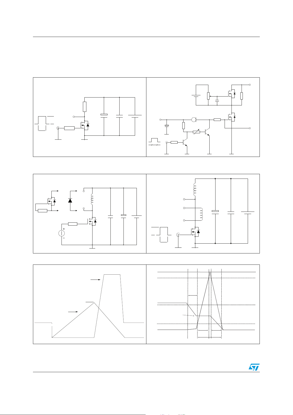
3 Test circuits
Figure 2. Switching times test circuit for
resistive load
Figure 4. Test circuit for inductive load
switching and diode recovery times
Figure 3. Gate charge test circuit
Figure 5. Unclamped inductive load test
circuit
L
VD
2200
μF
3.3
μF
VDD
ID
Vi
D.U. T.
Pw
Figure 6. Unclamped inductive waveform Figure 7. Switching time waveform
Id
90%Vds
t
d
(v)
Vgs
90%Vgs
on
on
))
Vgs(I(t))
10%Vds
6/14 Doc ID 023799 Rev 2
Vds
r
(v)
t
AM01471v1
Inductive Load Turn
f
(i)
t
t
c
(off)
-off
90%Id
10%Id
AM05540v1
Page 7

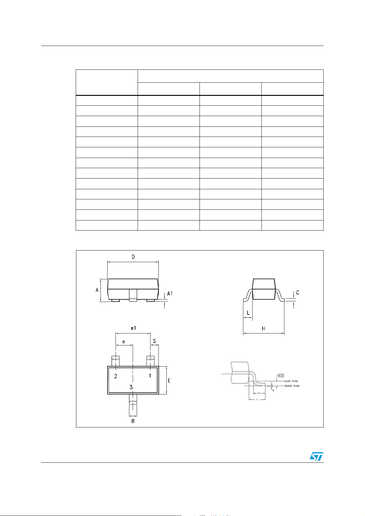
STR2N2VH5, STT5N2VH5 Package mechanical data
4 Package mechanical data
In order to meet environmental requirements, ST offers these devices in different grades of
ECOPACK
specifications, grade definitions and product status are available at: www.st.com.
ECOPACK
®
packages, depending on their level of environmental compliance. ECOPACK®
®
is an ST trademark.
Doc ID 023799 Rev 2 7/14
Page 8
Package mechanical data STR2N2VH5, STT5N2VH5
0053390_I
Table 8. SOT-23 mechanical data
mm
Dim.
Min. Typ. Max.
A0.89 1.40
A1 0 0.10
B0.30 0.51
C 0.085 0.18
D2.75 3.04
e0.85 1.05
e1 1.70 2.10
E1.20 1.75
H2.10 3.00
L0.60
S0.35 0.65
L1 0.25 0.55
a0° 8°
Figure 8. SOT-23 mechanical drawing
8/14 Doc ID 023799 Rev 2
Page 9
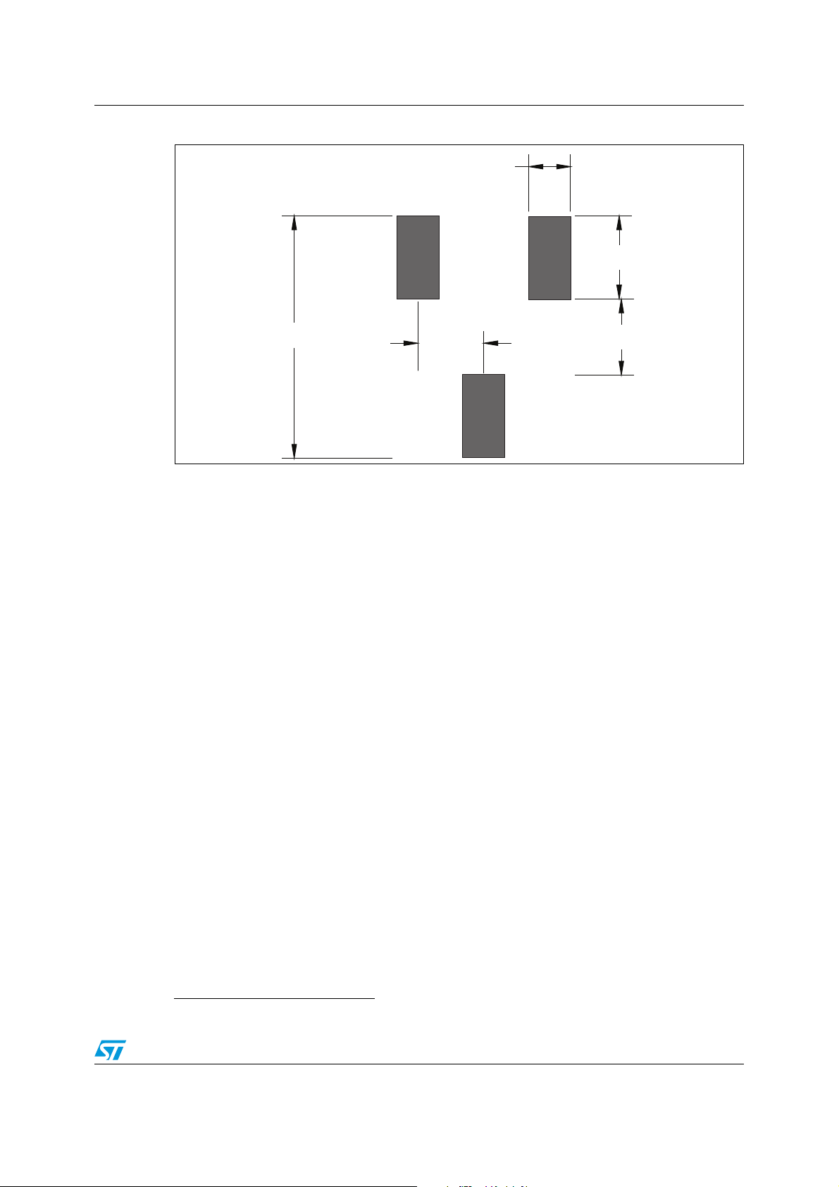
STR2N2VH5, STT5N2VH5 Package mechanical data
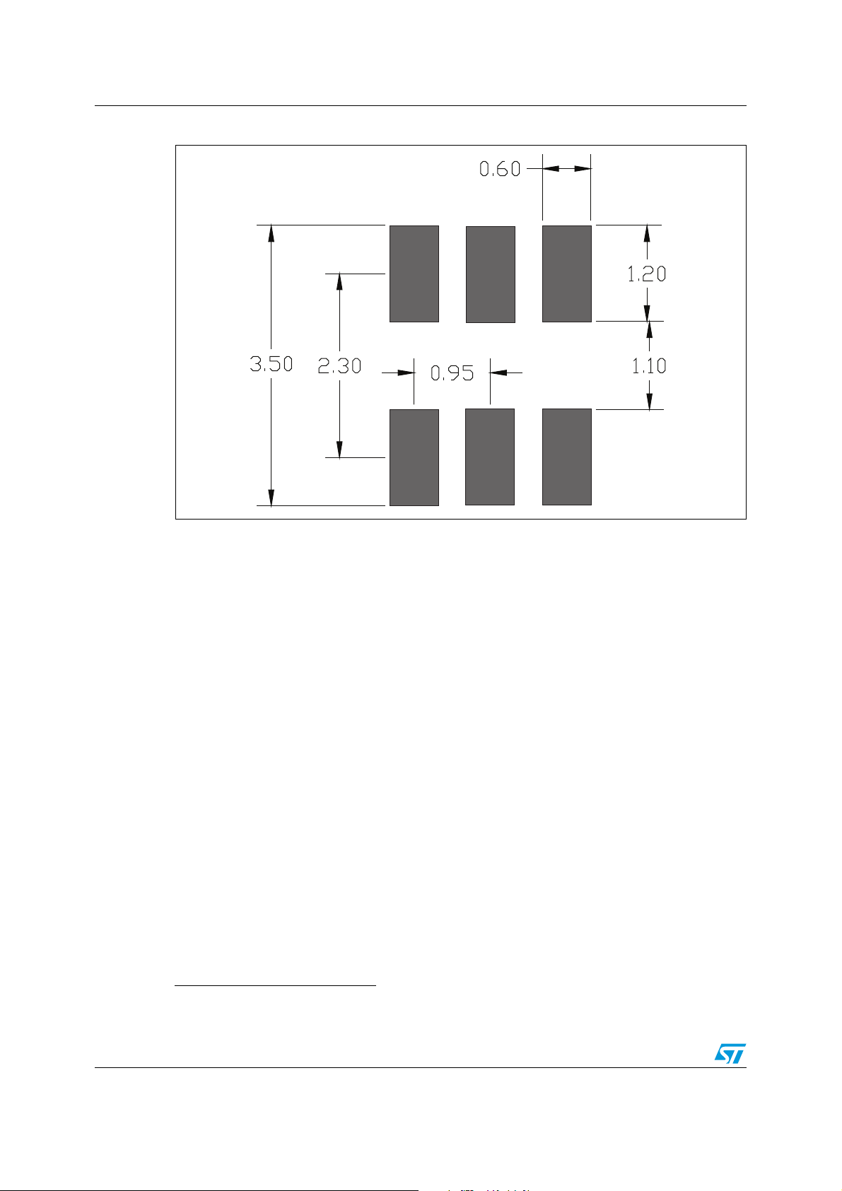
2.89
0.95
0.48
0.97
0.99
SOT-23 footp_I
Figure 9. SOT-23 recommended footprint
(a)
a. Dimensions are in mm.
Doc ID 023799 Rev 2 9/14
Page 10
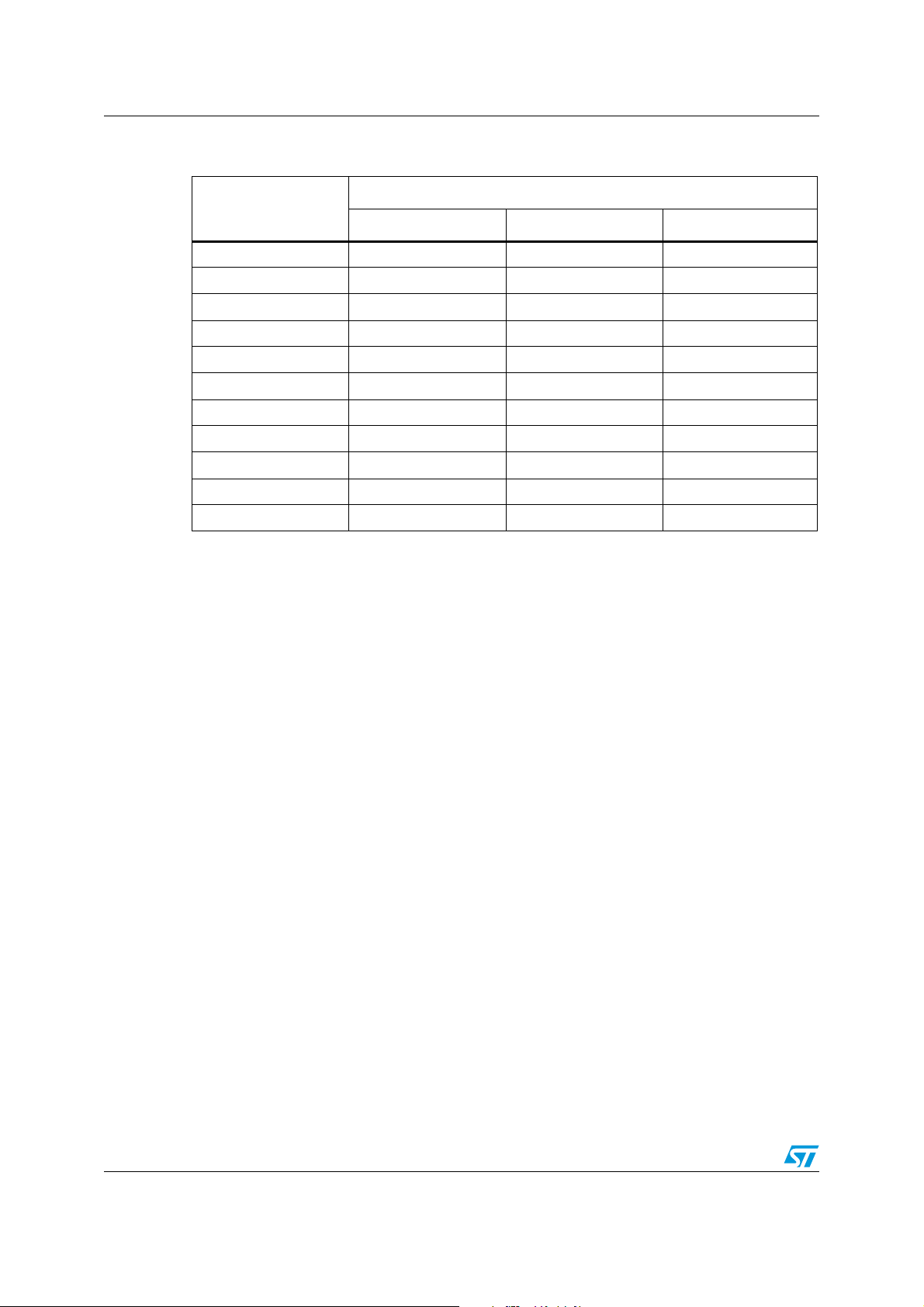
Package mechanical data STR2N2VH5, STT5N2VH5
Table 9. SOT23-6L package mechanical data
mm
Dim.
Min. Typ. Max.
A 0.90 1.45
A1 0.00 0.15
A2 0.90 1.30
b 0.30 0.50
C 0.09 0.20
D 2.80 3.05
E 1.50 1.75
e0.95
H 2.60 3.00
L 0.30 0.60
φ 0° 10°
10/14 Doc ID 023799 Rev 2
Page 11

STR2N2VH5, STT5N2VH5 Package mechanical data
7049714_I
Figure 10. SOT23-6L package drawing
Doc ID 023799 Rev 2 11/14
Page 12
Package mechanical data STR2N2VH5, STT5N2VH5
SOT-23-6L footp_I
Figure 11. SOT23-6L recommended footprint
(b)
b. All dimensions are in millimeters
12/14 Doc ID 023799 Rev 2
Page 13
STR2N2VH5, STT5N2VH5 Revision history
5 Revision history
Table 10. Document revision history
Date Revision Changes
19-Oct-2012 1 First release.
14-Jan-2013 2 Modified: R
DS(on)
values
Doc ID 023799 Rev 2 13/14
Page 14

STR2N2VH5, STT5N2VH5
Please Read Carefully:
Information in this document is provided solely in connection with ST products. STMicroelectronics NV and its subsidiaries (“ST”) reserve the
right to make changes, corrections, modifications or improvements, to this document, and the products and services described herein at any
time, without notice.
All ST products are sold pursuant to ST’s terms and conditions of sale.
Purchasers are solely responsible for the choice, selection and use of the ST products and services described herein, and ST assumes no
liability whatsoever relating to the choice, selection or use of the ST products and services described herein.
No license, express or implied, by estoppel or otherwise, to any intellectual property rights is granted under this document. If any part of this
document refers to any third party products or services it shall not be deemed a license grant by ST for the use of such third party products
or services, or any intellectual property contained therein or considered as a warranty covering the use in any manner whatsoever of such
third party products or services or any intellectual property contained therein.
UNLESS OTHERWISE SET FORTH IN ST’S TERMS AND CONDITIONS OF SALE ST DISCLAIMS ANY EXPRESS OR IMPLIED
WARRANTY WITH RESPECT TO THE USE AND/OR SALE OF ST PRODUCTS INCLUDING WITHOUT LIMITATION IMPLIED
WARRANTIES OF MERCHANTABILITY, FITNESS FOR A PARTICULAR PURPOSE (AND THEIR EQUIVALENTS UNDER THE LAWS
OF ANY JURISDICTION), OR INFRINGEMENT OF ANY PATENT, COPYRIGHT OR OTHER INTELLECTUAL PROPERTY RIGHT.
UNLESS EXPRESSLY APPROVED IN WRITING BY TWO AUTHORIZED ST REPRESENTATIVES, ST PRODUCTS ARE NOT
RECOMMENDED, AUTHORIZED OR WARRANTED FOR USE IN MILITARY, AIR CRAFT, SPACE, LIFE SAVING, OR LIFE SUSTAINING
APPLICATIONS, NOR IN PRODUCTS OR SYSTEMS WHERE FAILURE OR MALFUNCTION MAY RESULT IN PERSONAL INJURY,
DEATH, OR SEVERE PROPERTY OR ENVIRONMENTAL DAMAGE. ST PRODUCTS WHICH ARE NOT SPECIFIED AS "AUTOMOTIVE
GRADE" MAY ONLY BE USED IN AUTOMOTIVE APPLICATIONS AT USER’S OWN RISK.
Resale of ST products with provisions different from the statements and/or technical features set forth in this document shall immediately void
any warranty granted by ST for the ST product or service described herein and shall not create or extend in any manner whatsoever, any
liability of ST.
ST and the ST logo are trademarks or registered trademarks of ST in various countries.
Information in this document supersedes and replaces all information previously supplied.
The ST logo is a registered trademark of STMicroelectronics. All other names are the property of their respective owners.
© 2013 STMicroelectronics - All rights reserved
STMicroelectronics group of companies
Australia - Belgium - Brazil - Canada - China - Czech Republic - Finland - France - Germany - Hong Kong - India - Israel - Italy - Japan -
Malaysia - Malta - Morocco - Philippines - Singapore - Spain - Sweden - Switzerland - United Kingdom - United States of America
www.st.com
14/14 Doc ID 023799 Rev 2
Page 15

 Loading...