

Page 1

®
MAIN PRODUCT CHARACTERISTICS
STPS340U/S/B
POWER SCHOTTKY RECTIFIER
I
F(AV)
V
RRM
3 A
40 V
Tj (max) 150 °C
(max) 0.57 V
V
F
VERY SMALL CONDUCTION LOSSES
NEGLIGIBLE SWITCHING LOSSE S
LOW FORWARD V O LTAGE DROP
LOW THERMAL RE SISTA NCE
EXTREMELY FAST SWITCHING
SURFACE MOUNTED DEVICE
DESCRIPTION
Single chip Schottky rectifier suited for Switch
Mode Power Supplies and high frequency DC to
DC converters.
Packaged in SMB, SMC and DPAK this device is
intended for use in low and medium voltage
operation, high frequency inverters, free wheeling
and polarity protection applications where low
switching losses are required.
K
SMB
(JEDEC DO -214AA)
STPS340U
A
NC
DPAK
STPS340B
SMC
(JEDEC DO-214AB)
STPS340S
ABSOLUTE RATINGS (limiting values)
Symbol Parameter Value Unit
V
RRM
I
F(RMS)
I
F(AV)
I
FSM
Repetitive peak reverse voltage
RMS forward current DPAK
SMB / SMC
= 135°C δ = 0.5
T
Average forward current
Surge non repetitive forward
c
= 105°C δ = 0.5
T
L
tp = 10 ms Sinusoidal
DPAK
SMB / SMC
40 V
6A
10
3
75 A
current
I
RRM
Repetitive peak reverse
tp = 2 µs F = 1kHz square
1A
current
Tstg
Tj
dV/dt
June 1999 - Ed: 6B
Storage temperature range
Maximum operating junction temperature
Critical rate of rise of r ever se voltage
- 65 to + 150 °C
+ 150 °C
10000 V/µs
A
1/7
Page 2

STPS340U/S/B
THERMAL R E SI ST A NCES
Symbol Parameter Value Unit
R
th (j-l)
Junction to leads SMC
SMB
R
th (j-c)
Junction to case DPAK
STATIC ELECTRICAL CHARACTERISTI CS
Symbol Tests Conditions Tests Conditions Min. Typ. Max. Unit
*
I
R
V
Reverse leakage current
*
F
Forward voltage drop
Pulse test : * tp = 380 µs, δ < 2 %
Tj = 25°CV
Tj = 125°CV
Tj = 25°CI
Tj = 25°CI
Tj = 125°CI
Tj = 125°CI
= V
R
= V
R
= 3 A
F
= 6 A
F
= 3 A
F
= 6 A
F
RRM
RRM
20 °C/W
25
5.5 °C/ W
20 µA
210mA
0.63 V
0.84
0.52 0.57
0.63 0.72
To evaluate the maximum conduction losses use the follo wing equation :
P = 0.42 x I
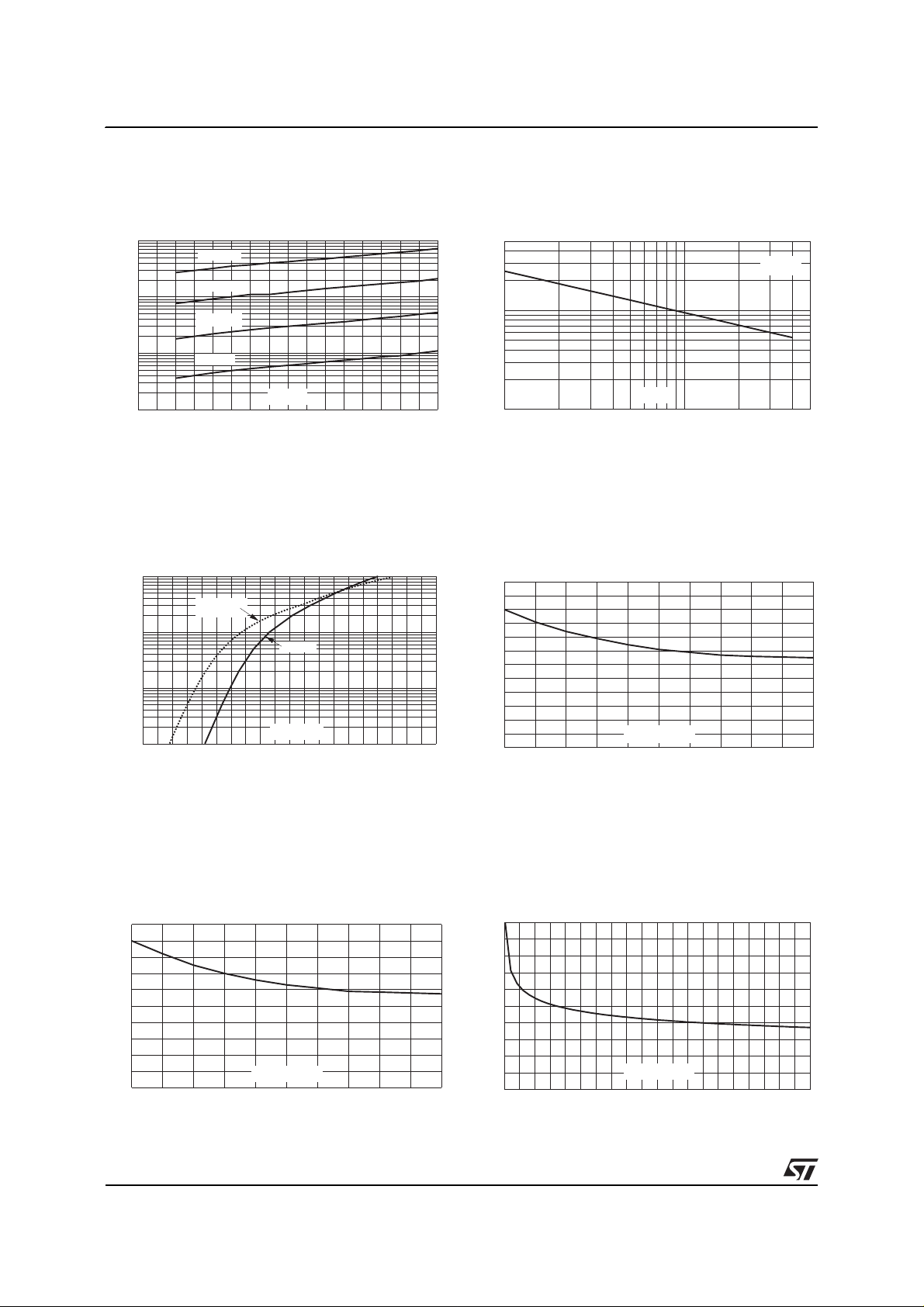
Fig. 1: Average forward power dissipation versus
average forward current.
PF(av)(W)
2.5
2.0
1.5
1.0
0.5
0.0
0.0 0.5 1.0 1.5 2.0 2.5 3.0 3.5 4.0
F(AV)
δ = 0.05
+ 0.050 I
δ = 0.1
F2(RMS)
δ = 0.2
IF(av) (A)
δ = 0.5
δ
=tp/T
δ = 1
Fig. 2: Average current versus ambient
temperature (δ =0.5).
IF(av)(A)
3.5
3.0
2.5
Rth(j-a)=65°C/W
2.0
1.5
T
tp
1.0
0.5
0.0
0 25 50 75 100 125 150
δ
=tp/T
Rth(j-a)=Rth(j-c)
(DPAK)
Rth(j-a)=Rth(j-l)
(SMB/SMC)
T
tp
Tamb(°C)
2/7
Page 3

STPS340U/S/B
Fig. 3-1: Non repetit iv e s urge peak forward current
versus overload duration (SMB)(Maximum values).
IM(A)
10
9
8
7
6
5
4
3
I
M
2
1
0
1E-3 1E-2 1E-1 1E+0
t
δ
=0.5
t(s)
Ta=25°C
Ta=50°C
Ta=100°C
Fig. 3-3: Non repetitive surge peak forward current
versus overload duration (DPAK) (Maximum
values).
IM(A)
50
40
30
20
I
M
10
0
1E-3 1E-2 1E-1 1E+0
t
δ
=0.5
t(s)
Tc=25°C
Tc=50°C
Tc=100°C
Fig. 3- 2 : Non repetitive surge peak forward current
versus overload duration (SMC) (Maximum values).
IM(A)
12
10
8
Ta=25°C
6
4
I
M
2
0
1E-3 1E-2 1E-1 1E+0
t
δ
=0.5
t(s)
Ta=50°C
Ta=100°C
Fig. 4-1: Relative variation of thermal transient
impedance junction to lead versus pulse duration
(SMB).
Zth(j-a)/Rth(j-a)
1.0
Printed circuit board (e=35µm)
0.9
0.8
0.7
0.6
0.5
δ = 0.5
0.4
0.3
0.2
δ = 0.2
δ = 0.1
0.1
0.0
1.0E-2 1.0E-1 1.0E+0 1.0E+1 1.0E+2 1.0E+3
Single pulse
tp(s)
δ
=tp/T
T
tp
Fig. 4-2: Relative variation of thermal transient
impedance junction to lead versus pulse duration
(SMC).
Zth(j-a)/Rth(j-a)
1.0
Printed circuit board (e=35µm)
0.9
0.8
0.7
0.6
0.5
δ = 0.5
0.4
0.3
δ = 0.2
0.2
δ = 0.1
0.1
0.0
1.0E-2 1.0E-1 1.0E+0 1.0E+1 1.0E+2 1.0E+3
Single pulse
tp(s)
δ
=tp/T
T
tp
Fig. 4-3: Relative variation of thermal transient
impedance junction to lead versus pulse
duration(DPAK).
Zth(j-a)/Rth(j-a)
1.0
Printed circuit board (e=35µm)
0.9
0.8
0.7
0.6
δ = 0.5
0.5
0.4
δ = 0.2
0.3
δ = 0.1
0.2
Single pulse
0.1
0.0
1E-3 1E-2 1E-1 1E+0
tp(s)
δ
=tp/T
T
tp
3/7
Page 4
STPS340U/S/B
Fig. 5: Reverse leakage current versus reverse
voltage applied (Typical values).
IR(A)
1E-2
Tj=150°C
Tj=125°C
1E-3
Tj=100°C
1E-4
Tj=75°C
VR(V)
1E-5
0 5 10 15 20 25 30 35 40
Fig. 7: Forward voltage drop versus forward
current (Maximum values).
IFM(A)
10.00
Typical values
Tj=150°C
1.00
0.10
Tj=125°C
Fig. 6: Junction capacitance versus reverse
voltage applied (Typical values).
C(pF)
500
F=1MHz
200
100
50
20
10
12 51020 50
VR(V)
Tj=25°C
Fig. 8-1: Thermal resistance junction to ambient
versus co pper surface under e ach lead (Epoxy printed
circuit boa rd FR4, copper thickness: 35 µm) (SMB).
Rth(j-a) (°C/W)
120
100
80
60
40
0.01
0.0 0.1 0.2 0.3 0.4 0.5 0.6 0.7 0.8 0.9 1.0
VFM(V)
Fig. 8-2: Thermal resistance junction to ambient
versus copp er surface under ea ch lead (Epoxy printed
circuit boar d FR4, copper thickness: 35µ m ) (S MC) .
Rth(j-a) (°C/W)
100
80
60
40
20
0
012345
S(Cu) (cm²)
20
0
012345
S(Cu) (cm²)
Fig. 8-3: Thermal resistance junction to ambient
versus c opper surf ace under eac h lead ( Epo xy p rinted
circ uit board FR 4, coppe r thicknes s: 35µm) (DPAK).
Rth(j-a) (°C/W)
100
80
60
40
20
0
02468101214161820
S(Cu) (cm²)
4/7
Page 5

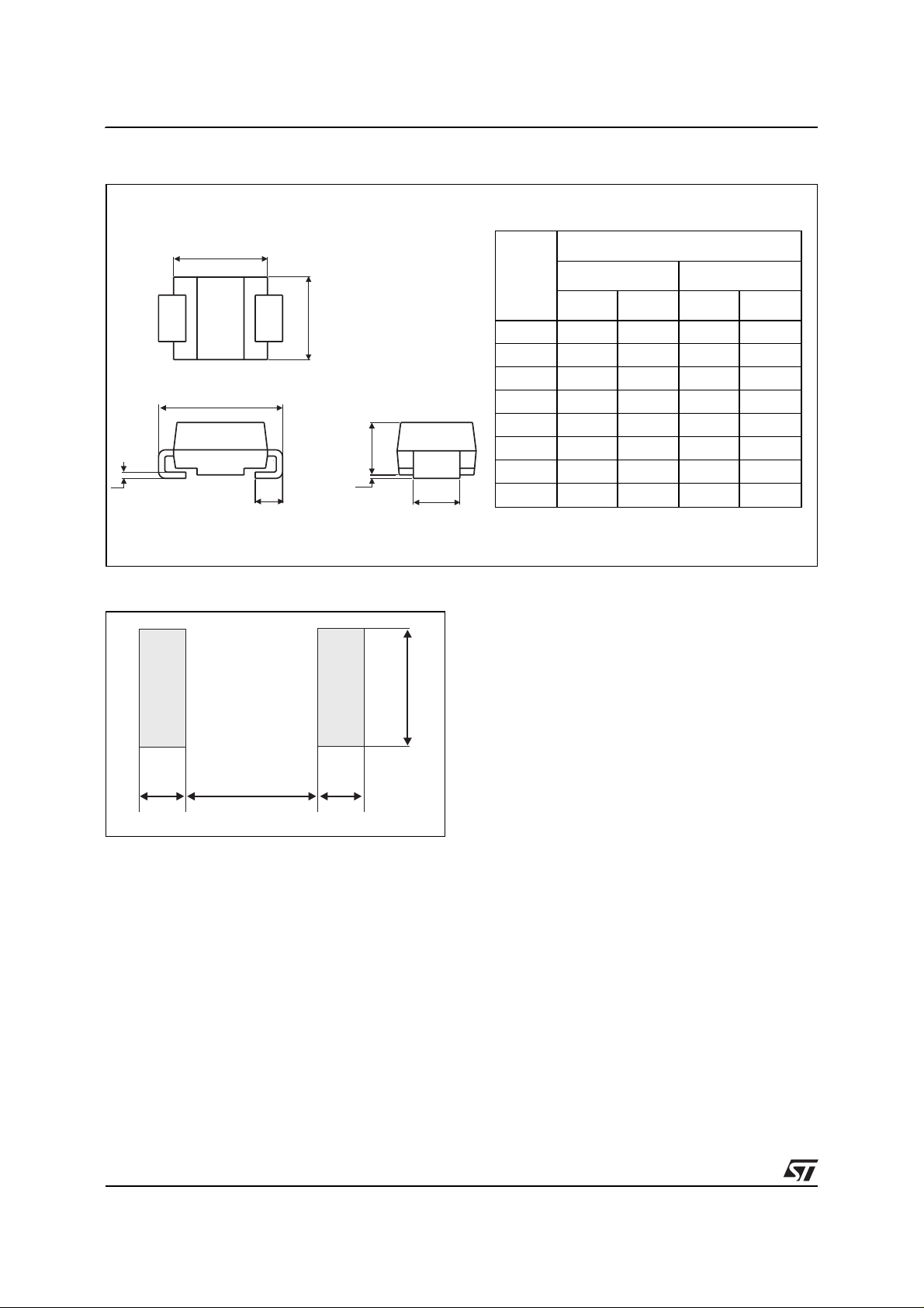
PACKAGE ME CHANICAL D AT A
DPAK
STPS340U/S/B
DIMENSIONS
REF.
A 2.20 2.40 0.086 0.094
A1 0.90 1.10 0.035 0.043
A2 0.03 0.23 0.001 0.009
B 0.64 0.90 0.025 0.035
B2 5.20 5.40 0.204 0.212
C 0.45 0.60 0.017 0.023
C2 0.48 0.60 0.018 0.023
D 6.00 6.20 0.236 0.244
E 6.40 6.60 0.251 0.259
G 4.40 4.60 0.173 0.181
H 9.35 10.10 0.368 0.397
L2 0.80 typ. 0.031 typ.
L4 0.60 1.00 0.023 0.039
V2 0° 8° 0° 8°
Millimeters Inches
Min. Max Min. Max.
FOOTPRINT DIMENSIONS (in millimeters)
6.7
6.7
3
3
1.61.6
2.32.3
5/7
Page 6
STPS340U/S/B
PACKAGE ME CHANICAL D AT A
SMB
E1
D
E
A1
C
L
A2
FOOTPRINT DIMENSIONS (in millimeters)
2.3
DIMENSIONS
REF.
Millimeters Inches
Min. Max. Min. Max.
A1 1.90 2.45 0.075 0.096
A2 0.05 0.20 0.002 0.008
b 1.95 2.20 0.077 0.087
c 0.15 0.41 0.006 0.016
E 5.10 5.60 0.201 0.220
E1 4.05 4.60 0.159 0.181
D 3.30 3.95 0.130 0.156
b
L 0.75 1.60 0.030 0.063
1.52 2.75
6/7
1.52
Page 7

PACKAGE ME CHANICAL D AT A
SMC
STPS340U/S/B
E1
D
E
A1
C
E2
L
A2
FOOTPRINT DIMENSIONS (in millimeters)
3.3
DIMENSIONS
REF.
Millimeters Inches
Min. Max. Min. Max.
A1 1.90 2.45 0. 075 0.096
A2 0.05 0.20 0. 002 0.008
b 2.90 3.2 0.114 0.126
c 0.15 0.41 0.006 0.016
E 7.75 8.15 0.305 0.321
E1 6.60 7.15 0.260 0.281
E2 4.40 4.70 0.173 0.185
D 5.55 6.25 0.218 0.246
L 0.75 1.60 0.030 0.063
b
2.0 4.2 2.0
Ordering type Marking P ackage Weight Base qty Delivery mode
STPS340U U34 SMB 0.107g 2500 Tape and reel
STPS340S S34 SMC 0.243g 2500 Tape and reel
STPS340B S 340 DPAK 0.30g 75 Tube
STPS340B-TR S340 DPAK 0.30g 2500 Tape and reel
Band indicates cathode on SMB, SMC
Epoxy meets UL94,V0
Information furnished is believed to be accurate and reliable. However, STMicroelectronics assumes no responsibility for the conseq uences of
use of such information nor for any infringement of patents or other rights of third parties which may result from its use. No license is granted by
implication or otherwis e under any patent or patent rights of STMicroelectro nics. Specifications men tioned in this publication are subject to
change without notice. This publication supersedes and replaces all information previously supplied.
STMicroelectro nic s products are not authorized for us e as critical com ponents in life support devi ces or systems wi th out ex press written approval of STMicroelectronics.
The ST logo is a registered trademark o f STMicroelectron ics
© 1999 STMicroelectronics - Printed in Italy - All rights reserved.
STMicroelectronics GROUP OF COMPANIES
Australia - Brazil - China - Finland - France - Germany - Hong Kong - India - Italy - Japan - Malaysia
Malta - Morocco - Singapore - Spain - Sweden - Switzerland - United Kingdom - U.S.A.
http://www.st.com
7/7
Page 8

This datasheet has been download from:
www.datasheetcatalog.com
Datasheets for electronics components.
 Loading...