

Page 1
UM2847
User manual
EVALSTPM-3PHISO: Getting started with the STPMS2 3-ph full shunt evaluation
board
Introduction
The EVALSTPM-3PHISO evaluation board implements a 3-phase AC Watt meter that meets accuracy class 0.5 according to
IEC 62053-22 standard using low-cost, electromagnetic-immune shunt sensors and advanced galvanic-isolation technology.
The evaluation board combines the high-accuracy STPMS2 metering front-end IC and the STISO621 digital isolator with
customizable firmware running on an STM32 microcontroller to compute metrology and power-quality data.
The STPMS2, a two-channel 24-bit second-order, sigma-delta modulator, measures voltage and current for each phase through
an on-board voltage divider and a shunt current sensor. It oversamples the signal using a synchronized 4 MHz clock distributed
by the microcontroller and multiplexes voltage and current sigma-delta bitstreams on a single output pin. Three STPMS2 are
used in the 3-phase system to collect voltage and current data from each phase.
The STISO621, a dual-channel digital isolator based on a 6 kV thick-oxide, galvanic-isolation technology, transfers data
between isolated domains and guarantees 6 kV VIOTM and 1.2 kV VIORM between the phases.
The FW implemented on the STPM32F413 uses digital filters for sigma-delta modulator (DFSDM) peripheral to demultiplex the
six bitstreams, convert them into 24-bit voltage and current values, and computes all metrology data in real-time every 200 µs.
The firmware also implements a Virtual COM port that provides access to internal parameters for reading metrology data,
modifying the internal configuration, and calibrating the board.
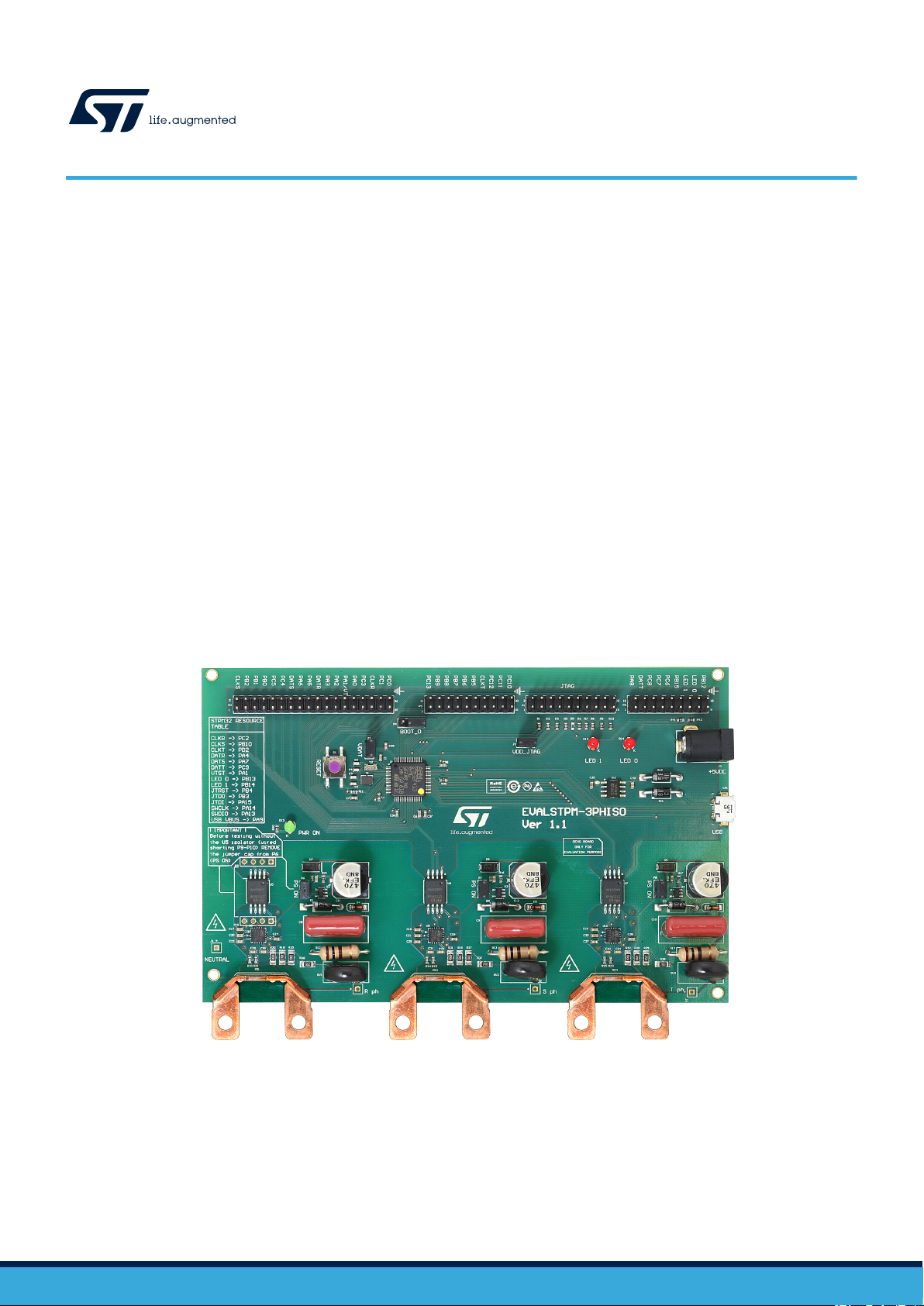
Figure 1. EVALSTPM-3PHISO image
UM2847 - Rev 1 - March 2021
For further information contact your local STMicroelectronics sales office.
www.st.com
Page 2

1 Safety and operating instructions
1.1 General terms
Warning:
During assembly, testing, and operation, the evaluation board poses inherent hazards due to high
voltage.
Danger:
There is danger of serious personal injury, property damage or death due to electrical shock if the
kit or components are improperly used or installed incorrectly.
The kit is not electrically isolated from the high-voltage supply AC/DC input. The evaluation board is
directly linked to the mains voltage. No barrier is present between the accessible parts and the high
voltage. All measuring equipment must be isolated from the mains before powering the board. When
using an oscilloscope with the demo, it must be isolated from the AC line. This prevents shock from
occurring as a result of touching any single point in the circuit, but does NOT prevent shock when
touching two or more points in the circuit.
All operations involving transportation, installation and use, and maintenance must be performed by skilled
technical personnel able to understand and implement national accident prevention regulations. For the purposes
of these basic safety instructions, “skilled technical personnel” are suitably qualified people who are familiar with
the installation, use and maintenance of power electronic systems.
UM2847
Safety and operating instructions
1.2 Intended use of evaluation board
The evaluation board is designed for demonstration purposes only. Technical data and information concerning the
power supply conditions are detailed in the documentation and should be strictly observed.
1.3 Installing the evaluation board
The board contains electrostatically-sensitive components that are prone to damage if used incorrectly. Do not
mechanically damage or destroy the electrical components (potential health risks).
1.4 Operating the evaluation board
To operate properly the board, follow these safety rules.
1. Work area safety:
– The work area must be clean and tidy.
– Do not work alone when boards are energized.
– Protect against inadvertent access to the area where the board is energized using suitable barriers and
signs.
– A system architecture that supplies power to the evaluation board must be equipped with additional
control and protective devices in accordance with the applicable safety requirements (i.e., compliance
with technical equipment and accident prevention rules).
– Use non-conductive and stable work surface.
– Use adequately insulated clamps and wires to attach measurement probes and instruments.
UM2847 - Rev 1
page 2/20
Page 3
Operating the evaluation board
2. Electrical safety:
– Proceed with the arrangement of measurement set-up, wiring or configuration paying attention to high
voltage sections.
– Remove power supply from the board and electrical loads before performing any electrical
measurement on the high voltage sections of the board.
– Once the set-up is complete, energize the board.
Danger:
Do not touch the evaluation board when it is energized or immediately after it has been
disconnected from the voltage supply as several parts and power terminals containing potentially
energized capacitors need time to discharge.
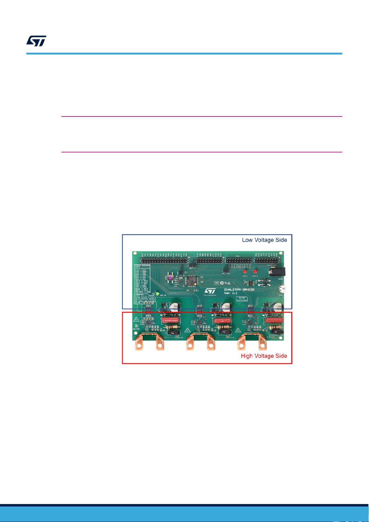
Parts of the kit are not electrically isolated from the AC/DC input. The USB interface, the JTAG
connector and the strip line connector are in the low voltage side of the board, so they can be used to
connect a host computer. Please refer to Figure 2.
3. Personal safety :
– Always wear suitable personal protective equipment such as insulating gloves and safety glasses.
– Take adequate precautions and install the board in such a way to prevent accidental touch. Use
protective shields such as an insulating box with interlocks if necessary.
Figure 2. High and low voltage sides
UM2847
UM2847 - Rev 1
page 3/20
Page 4
2 Getting started
2.1 Hardware and software requirements
Using the EVALSTPM-3PHISO evaluation board requires the following software and hardware:
• A Windows PC (XP, Vista, Win 7, Win 8, Win 10) to eventually install the software package available on
www.st.com (optional) or to communicate through the mini-shell
• A 'USB type A to Micro-B' cable, used to power on the board (through USB connector CN1) from host PC
and to allow communication with terminal or software GUI
• JTAG arm debugging probe (optional)
• 3-Ph AC power supply and 3-Ph load
• Reference meter (optional)
The system could be run and evaluated in the following ways:
• Installing the software GUI STSW-STPM005 from www.st.com . In this case please refer to the related
documentation.
• Connecting to a shell terminal on the host PC
• Using a JTAG arm debugging probe which can be connected to JTAG connector for debugging and
programming. For this purpose, it is necessary to install the IDE “IAR embedded workbench for ARM”
version 8.5.
UM2847
Getting started
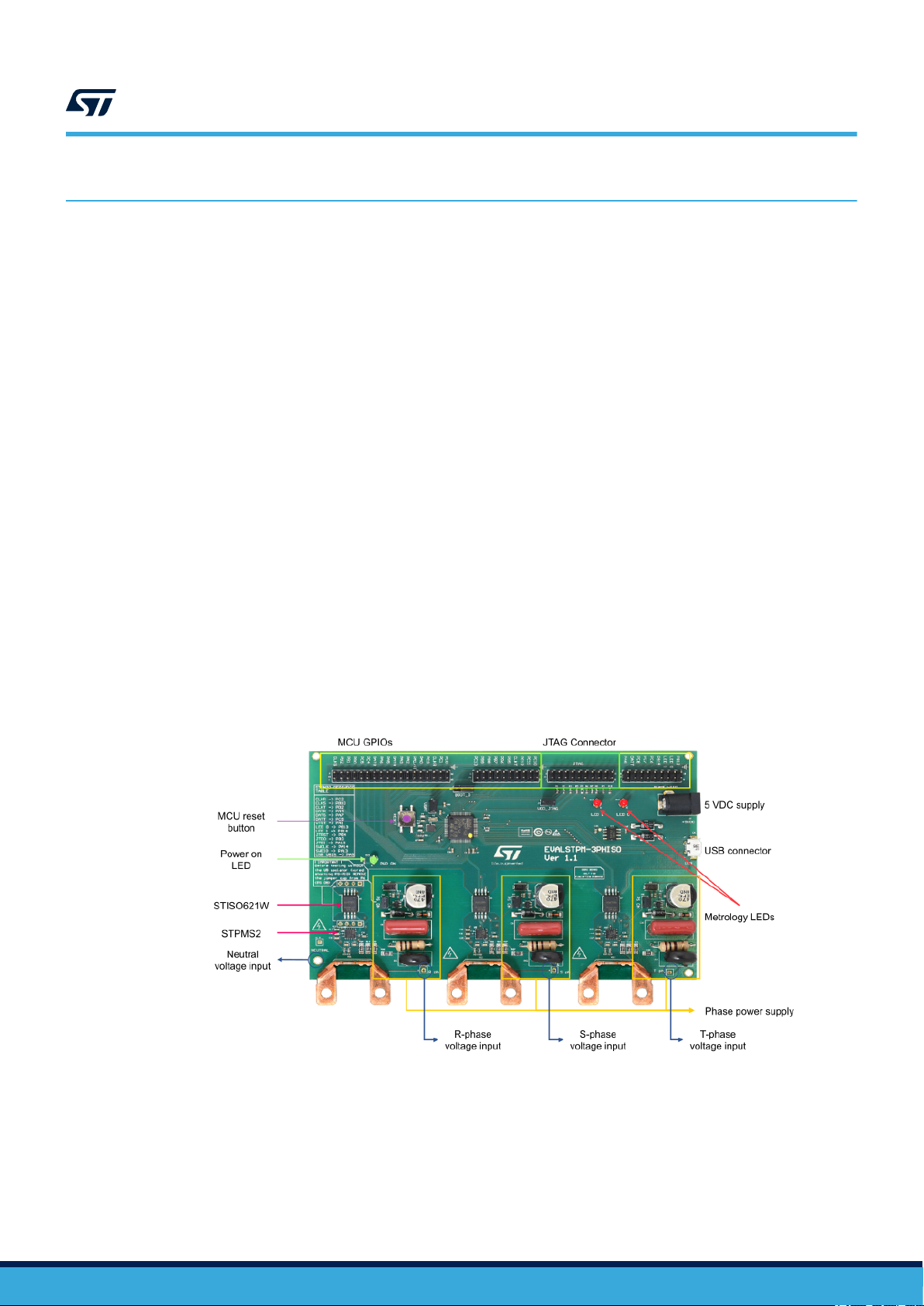
2.2 Hardware description
Figure 3. EVALSTPM-3PHISO board function description
2.2.1 Power supply
The board can be supplied alternatively by:
• connecting a USB cable to the PC
• providing 5 VDC by the coaxial jack
UM2847 - Rev 1
page 4/20
Page 5

Each phase STPMS2 is supplied by an independent capacitive power supply, providing the necessary 3.3 V to
the device. The jumpers P4, P7 and P8 must remain fit to use the power supply, otherwise it is bypassed.
2.2.2 Voltage and current sensing section
The STPMS2 devices onboard are configured as follows:
Table 1. STPMS2 HW configuration
PIN Connection Description
MS0 VCC HPR, amplifier GAIN selection g3 = 16
MS1 GND TC = 50 ppm/°C
MS2 GND Voltage channel ON, DATn = ~ [DAT =(CLK) ? bsV : bsC)]
MS3 GND Hard mode, BIST mode OFF
Note: For further information on STPMS2 configuration please refer to device datasheet.
The metrology section analog front-end component values are as follows:
UM2847
Running the built-in demonstration
Table 2. AFE components
Component Value Description
Shunt 0.3 mOhm Current sensor
R1 810 kOhm Voltage divider resistor (actually 3 x 270 kOhm)
R2 470 Ohm Voltage divider resistor
2.2.3 Board ratings
The ratings of the board, given by the parameters specified above, are as follows:
• Power stage supply voltage between 80 V RMS and 350 V RMS
• Maximum load current 86 A RMS
2.3 Running the built-in demonstration
The board comes with the demonstration firmware preloaded in the Flash memory. Please make sure to
download and use the latest release of STSW-STPM004 firmware from www.st.com.
Before running the application, the user should establish the connection with the 3-phase full shunt board.
Follow the steps below to run it:
• Connect the board to a PC with a 'USB type A to Micro-B' cable through USB connector CN1 to power the
board. Green LED (PWR ON) then lights up.
• First connect the board to a 3-phase generator and load as shown in the figure below, then power on the
generator:
UM2847 - Rev 1
page 5/20
Page 6
Figure 4. Electric connections
UM2847
Running the built-in demonstration
• When the load is connected, LED0 and LED1 blink with a frequency proportional to respectively active and
reactive power consumption.
• Connect a shell terminal to the board Virtual COM port as specified in Section 4.3 below.
• Alternatively, use the software GUI STSW-STPM005 to read/calibrate the metrology data. For more details
on the Metrology GUI please refer to its user manual.
• For application development and debug, connect the JTAG probe and open “IAR Embedded Workbench for
ARM” IDE. For STSW-STPM004 FW details please refer to related user manual.
UM2847 - Rev 1
page 6/20
Page 7

3 Metrology application
3.1 Metrology calculations
The metrology features implemented by EVALSTPM-3PHISO FW are the following:
• 6 channels V-I decimated samples available every 200 us
• Line period and phase shift measurement for each phase
• Phase to phase voltage delays
• RMS and THD calculation (optional) of each V-I signal
• 1-ph Active wideband, active fundamental and reactive power/energy calculation
• 1-ph Apparent RMS power/energy calculation
• 3-ph Active wideband, active fundamental and reactive power/energy calculation
• 3-ph Apparent RMS power/energy calculation
• Data latch in STPM3x like registers
• Full calibration (amplitude, power offset and samples offset for DC measurement)
• DC measurement optional excluding high-pass filter on ADC data
• Status bits for power sign, frequency error and signal stuck
• Two configurable LEDs for pulsed outputs
• Interface to Metrology GUI through USB
UM2847
Metrology application
3.2
Power is a signed value, that can be expressed as a normalized value as:
p n
P
norm
Energy register is an up/down counter, always positive, that increases or decreases according to the power sign.
All metrology calculations are performed in real-time every 200 us, which is the signal sampling period.
Time registers, like period, V-C phase shift and phase to phase voltage delay have an LSB equal to 8 us.
For more information on the signal processing and register LSBs please refer to FW user manual.
−1 ∙ 228∙ p n 28 + p n 27: 0
=
28
2
Metrology registers
The data can be accessed in STPM32-like registers; data mapping in the registers is shown in Figure 5. Not all
the STPM32 registers are filled; only the used registers are shown.
UM2847 - Rev 1
page 7/20
Page 8

Figure 5. Registers map
ST Confidential
Address
(R)ead
(W)rite
(L)atch
Name
Default
Value
31 30 29 28 27 26 25 24 23 22 21 20 19 18 17 16 15 14 13 12 11 10 9 8 7 6 5 4 3 2 1 0
31 30 29 28 27 26 25 24 23 22 21 20 19 18 17 16 15 14 13 12 11 10 9 8 7 6 5 4 3 2 1 0
31 30 29 28 27 26 25 24 23 22 21 20 19 18 17 16 15 14 13 12 11 10 9 8 7 6 5 4 3 2 1 0
4 08 RW DSPCTRL5 00000800
5 0A RW DSPCTRL6 00000800
6 0C RW DSPCTRL7 00000000
7 0E RW DSPCTRL8 00000000
8 10 RW DSPCTRL9 00000000
9 12 RW DSPCTRL10 00000000
14 1C RW
V Freq ERR
V Signal
Stuck
C Signal
Stuck
RE_S
AF_S
AWB_S
DSPIRQ1 00000000
16 20 RWL
V Freq ERR
V Signal
Stuck
C Signal
Stuck
RE_S
AF_S
AWB_S
DSPSR1 00000000
21 2A R L
V Freq ERR
V Signal
Stuck
C Signal
Stuck
RE_S
AF_S
AWB_S
DSPEVENT1 00000000
23 2E RL DSP_REG1 00000000
24 30 RL DSP_REG2 00000000
25 32 RL DSP_REG3 00000000
28 38 RL DSP_REG6 00000000
29 3A R L DSP_REG7 00000000
32 40 RL DSP_REG10 00000000
33 42 RL DSP_REG11 00000000
36 48 RL DSP_REG14 00000000
37 4A R L DSP_REG15 00000000
38 4C RL DSP_REG16 00000000
39 4E RL DSP_REG17 00000000
42 54 RL CH1_REG1 00000000
43 56 RL CH1_REG2 00000000
44 58 RL CH1_REG3 00000000
45 5A R L CH1_REG4 00000000
46 5C RL CH1_REG5 00000000
47 5E RL CH1_REG6 00000000
48 60 RL CH1_REG7 00000000
49 62 RL CH1_REG8 00000000
51 66 RL CH1_REG10 00000000
52 68 RL CH1_REG11 00000000
66 84 RL TOT_REG1 00000000
67 86 RL TOT_REG2 00000000
68 88 RL TOT_REG3 00000000
69 8A R L TOT_REG4 00000000
DSPCTRL1
04000000
LPW1
[3:0]
31:28
27:24
23:20
19:16
15:12
11:8
7:4
3:0
LPS1
[1:0]
BHPFC1
BHPFV1
000RW
DSP Control Register #1
LCS1
[1:0]
204RW
DSP Control Register #3
DSPCTRL3
00000000
DSPCTRL2
24000000
LPW2
[3:0]
LCS2
[1:0]
102RW
DSP Control Register #2
LPS2
[1:0]
CHV [11:0]
CHC [11:0]
Padding
Padding
OFFV [23:0]
OFFC [23:0]
LATCH
REF_FREQ
LED2OFF
LED1OFF
Auto LATCH
OFAF [9:0]
OFA [9:0]
OFS [9:0]
OFR [9:0]
V Period [11:0]
Padding
V Sample [23:0]
Padding
C Sample [23:0]
THD V
THD C
Padding
V Fund Sample [23:0]
Padding
C Fund Sample [23:0]
1-PH Active Power[28:0]
V-C Angle [11:0]
C RMS Data [16:0]
C Fund RMS Data [16:0]
V RMS Data [14:0]
V Fund RMS Data [14:0]
V_V Delay[15:0]
3-PH Active Energy
3-PH Fundamental Energy
3-PH Reactive Energy
3-PH Apparent Energy
Padding
1-PH Momentary Active Power[28:0]
Padding
1-PH Momentary Fundamental Power[28:0]
Padding
1-PH Fundamental Power[28:0]
Padding
1-PH Reactive Power[28:0]
Padding
1-PH Apparent RMS Power[28:0]
1-PH Active Energy
1-PH Fundamental Energy
1-PH Reactive Energy
1-PH Apparent Energy
Padding
UM2847
Metrology registers
In the registers map, registers are divided in:
1. Configuration and calibration registers:
– Red field registers configure application LEDs and reference frequency. Since these configurations
refer to the whole application and are common to all the phases, they must be set only in the first
phase configuration registers.
– Yellow fields contain calibration and configuration data specific for each phase, so they must be set in
2. Data registers, indicated in blue, contain calculated data; they are all computed by the processing kernel on
UM2847 - Rev 1
each phase configuration register.
All the configuration registers, both application and phase ones, are written by the application and not
modified by the processing kernel. They can be configured in one of the following ways:
– either by setting them in the metroDefaultNvm in the handler_metrology.c file (please refer to FW user
– or at runtime by sending a write command (please refer to Section 3.3 below).
a 200 us basis, but updated in the registers upon request by setting the Latch bit in DSPCTRL3. Setting the
AutoLatch bit instead, these data are automatically updated every 200 us.
manual for details)
page 8/20
Page 9

3.2.1 Registers description
Bit Config. Description Default
19 BHPFV
20 BHPFC
24-27 LPW1
28-29 LPS1
30-31 LCS1
Table 3. DSP control register 1 (DSPCTRL1)
Bypass Hi-Pass Filter for voltage channel:
BHPFV = 0: HPF enabled
BHPFV = 1: HPF bypassed
Bypass Hi-Pass Filter for current channel:
BHPFC = 0: HPF enabled
BHPFC = 1: HPF bypassed
LED1 Speed Dividing Factor: 0x0 = 2-4, 0xF = 2
Default 0x4 = 1
LED1 pulse-out power selection:
LPS1 = 00: Active
LPS1 = 01: Active fundamental
LPS1 = 10: Reactive
LPS1 = 11: Apparent
LED1 pulse-out channel selection:
LCS1 = 00: Phase 1
LCS1 = 01: Phase 2
LCS1 = 10: Phase 3
LCS1 = 11: Three-phase
11
UM2847
Metrology registers
0x0
0x0
0x4
0x0
0x3
Bit
24-27 LPW2
28-29 LPS2
30-31 LCS2
Bit
21 Latch
Config. Description Default
Config. Description Default
Table 4. DSP control register 2 (DSPCTRL2)
LED2 Speed Dividing Factor: 0x0 = 2-4, 0xF = 2
Default 0x4 = 1
LED2 pulse-out power selection:
LPS2 = 00: Active
LPS2 = 01: Active fundamental
LPS2 = 10: Reactive
LPS2 = 11: Apparent
LED2 pulse-out channel selection:
LCS2 = 00: Phase 1
LCS2= 01: Phase 2
LCS2 = 10: Phase 3
LCS2 = 11: Three-phase
11
Table 5. DSP control register 3 (DSPCTRL3)
Updates measurement registers
This bit is automatically set to zero after action
0x4
0x2
0x3
0x0
UM2847 - Rev 1
page 9/20
Page 10

UM2847
Metrology registers
Bit Config. Description Default
23 Auto Latch Updates measurement registers at 5 kHz 0x0
LED1 pin output disable
24 LED1OFF
25 LED2OFF
27 REF_FREQ
Bit Config. Description Default
0-11 CHV Calibration register of voltage channel 0x800
‘0’: LED1 output on
‘1’: LED1 output disabled
When the LED output is disabled the pin is set at low state
LED2 pin output disable
‘0’: LED2 output on
‘1’: LED2 output disabled
When the LED output is disabled the pin is set at low state
Reference line frequency:
‘0’: 50Hz,
‘1’: 60Hz
Table 6. DSP control register 5 (DSPCTRL5)
0x0
0x0
0x0
Table 7. DSP control register 6 (DSPCTRL6)
Bit
0-11 CHC Calibration register of current channel 0x800
Config. Description Default
Table 8. DSP control register 7 (DSPCTRL7)
Bit
0-23 OFV Offset compensation of voltage channel 0x800
Config. Description Default
Table 9. DSP control register 8 (DSPCTRL8)
Bit
0-23 OFC Offset compensation of current channel 0x800
Config. Description Default
Offset on voltage and current is added to ADC sample in case of DC measurement, then if the bit BHPF for the
respective signal is set. Offset register LSB is equal to voltage or current sample register LSB.
Table 10. DSP control register 9 (DSPCTRL9)
Bit
12-21 OFA Offset compensation of active wideband power 0x0
22-31 OFAF Offset compensation of active fundamental power 0x0
Config. Description Default
UM2847 - Rev 1
page 10/20
Page 11

UM2847
Metrology registers
Table 11. DSP control register 10 (DSPCTRL10)
Bit Config. Description Default
12-21 OFR Offset compensation of reactive power 0x0
22-31 OFS Offset compensation of apparent power 0x0
Power offset is added to its respective power value to compensate error at low current. This register LSB is equal
to four times power register LSB:
LSB
Table 12. DSP interrupt register (DSPIRQ1)
Bit Config. Description Default
12 AWB_S If set, upon event occurrence an interrupt variable is set 0x0
13 AF_S If set, upon event occurrence an interrupt variable is set 0x0
14 RE_S If set, upon event occurrence an interrupt variable is set 0x0
20 C Signal Stuck If set, upon event occurrence an interrupt variable is set 0x0
24 V Signal Stuck If set, upon event occurrence an interrupt variable is set 0x0
25 V Freq Err If set, upon event occurrence an interrupt variable is set 0x0
POFF
= 4*LSB
P
Table 13. DSP status register (DSPSR1)
Bit
12 AWB_S
13 AF_S
14 RE_S
20 C Signal Stuck
24 V Signal Stuck
25 V Freq Err
Config. Description Default
If set, active wideband power sign is negative
Set by the processing kernel, must be cleared by the application
If set, active fundamental power sign is negative
Set by the processing kernel, must be cleared by the application
If set, reactive power sign is negative
Set by the processing kernel, must be cleared by the application
If set, current signal bitstream is stuck to 1 or 0
Set by the processing kernel, must be cleared by the application
If set, current signal bitstream is stuck to 1 or 0
Set by the processing kernel, must be cleared by the application
If set, voltage frequency is out of the range [33 Hz, 83 Hz]
Set by the processing kernel, must be cleared by the application
0x0
0x0
0x0
0x0
0x0
0x0
Table 14. DSP live events register (DSPEV1)
Bit
12 AWB_S
13 AF_S
14 RE_S
20 C Signal Stuck If set, current signal bitstream is stuck to 1 or 0 0x0
Config. Description Default
If set, active wideband power sign is negative
Set and cleared by the processing kernel
If set, active fundamental power sign is negative
Set and cleared by the processing kernel
If set, reactive power sign is negative
Set and cleared by the processing kernel
0x0
0x0
0x0
UM2847 - Rev 1
page 11/20
Page 12

Bit Config. Description Default
Set and cleared by the processing kernel
24 V Signal Stuck
25 V Freq Err
If set, current signal bitstream is stuck to 1 or 0
Set and cleared by the processing kernel
If set, voltage frequency is out of the range [33 Hz, 83 Hz]
Set and cleared by the processing kernel
3.3 Register access through mini-shell
It is possible to access all the metrology data by connecting to the virtual serial COM port associated to the board
with the following settings:
• Baud rate: 115200
• Handshake: request to send
• Parity: none
• Data bits: 8
• Stop bits: 1
To communicate with the board use the command set in Table 15, where:
• <phase> could be 1, 2 or 3;
• <address> is the address or the register to read, as in the second column of the registers map in Figure 5 ;
• <n> is the number of registers to read, maximum is 70. Please consider that some of the registers are
unused, they are not listed in Figure 5 but are actually present in the memory structure. It is necessary to
take them into account when requesting a read or write access on several registers.
UM2847
Register access through mini-shell
0x0
0x0
Table 15. Minishell commands
Command Data received
met metro 0 1 <phase> Voltage Period
met metro 6 1 <phase> 1 1 Current RMS
met metro 6 1 <phase> 2 1 Voltage RMS
met metro 17 1 <phase> 1 1 Fund Current RMS
met metro 17 1 <phase> 2 1 Fund Voltage RMS
met metro 18 1 <phase> 1 Current THD
met metro 18 1 <phase> 2 Voltage THD
met metro 7 1 <phase> Phase shift
met metro 19 1 <phase> V - V delay
met metro 1 1 <phase> 1 1-ph Active WB power
met metro 1 1 <phase> 2 1-ph Active Fund power
met metro 1 1 <phase> 3 1-ph Reactive power
met metro 1 1 <phase> 4 1-ph Apparent power
met metro 2 1 <phase> 1 1-ph Active WB energy
met metro 2 1 <phase> 2 1-ph Active Fund energy
met metro 2 1 <phase> 3 1-ph Reactive energy
met metro 2 1 <phase> 4 1-ph Apparent energy
met metro 20 1 1 3-ph Active WB energy
met metro 20 1 2 3-ph Active Fund energy
met metro 20 1 3 3-ph Reactive energy
UM2847 - Rev 1
page 12/20
Page 13

Register access through mini-shell
Command Data received
met metro 20 1 4 3-ph Apparent energy
met metro 21 1 <phase> All data
met rd <phase> <address> <Nb> Read < Nb > registers starting from <address>
met wr <phase> <address> <Nb> <data1> <data2> … <dataNb>
Write < Nb > registers starting from <address> ; <datax> is
the 32-bit register value to write
UM2847
UM2847 - Rev 1
page 13/20
Page 14

4 Accuracy results
-2
-1.5
-1
-0.5
0
0.5
1
1.5
2
0.001 0.01 0.1 1 10 100
3-ph AWB
phi = 0° phi = 60° phi =-60°
IEC Class 0.5 PF 0.5 Limits IEC Class 0.5 PF 1 Limits
The board needs to be calibrated to get target accuracy. For this purpose, it is possible to use the procedure
indicated in application note AN4470, “The STPM3x and the STCOMET application calibration”.
All the design and calibration formulas apply to the STPMS2 application as well, using the AFE parameters
reported in Table 2 and the application constants in Table 16.
An excel file with all the related formulas is available on request.
Parameter Value Unit Description
Vref 1.2 V Voltage reference value
Ai 16 Current channel gain
Au 2 Voltage channel gain
Cal_i 0.875 Calibrator mid value
Cal_v 0.875 Calibrator mid value
Dclk 5000 Hz Decimation frequency
UM2847
Accuracy results
Table 16. Application constants
Some of the accuracy test results after calibration are reported below:
Figure 6. Active wideband energy error over full scale current input range
UM2847 - Rev 1
page 14/20
Page 15

Figure 7. Current RMS error over full scale input range
-2.00%
-1.50%
-1.00%
-0.50%
0.00%
0.50%
1.00%
1.50%
2.00%
0.1 1 10 100
RMS Current
I1
I2
I3
UM2847
Accuracy results
UM2847 - Rev 1
page 15/20
Page 16

Revision history
UM2847
Table 17. Document revision history
Date Version Changes
10-Mar-2021 1 Initial release.
UM2847 - Rev 1
page 16/20
Page 17

UM2847
Contents
Contents
1 Safety and operating instructions ..................................................2
1.1 General terms .................................................................2
1.2 Intended use of evaluation board .................................................2
1.3 Installing the evaluation board....................................................2
1.4 Operating the evaluation board ...................................................2
2 Getting started ....................................................................4
2.1 Hardware and software requirements..............................................4
2.2 Hardware description ...........................................................4
2.2.1 Power supply ...........................................................4
2.2.2 Voltage and current sensing section ..........................................5
2.2.3 Board ratings............................................................5
2.3 Running the built-in demonstration ................................................5
3 Metrology application..............................................................7
3.1 Metrology calculations ..........................................................7
3.2 Metrology registers .............................................................7
3.2.1 Registers description......................................................9
3.3 Register access through mini-shell ...............................................12
4 Accuracy results .................................................................14
Revision history .......................................................................16
Contents ..............................................................................17
List of tables ..........................................................................18
List of figures..........................................................................19
UM2847 - Rev 1
page 17/20
Page 18

UM2847
List of tables
List of tables
Table 1. STPMS2 HW configuration ............................................................. 5
Table 2. AFE components ....................................................................5
Table 3. DSP control register 1 (DSPCTRL1).......................................................9
Table 4. DSP control register 2 (DSPCTRL2).......................................................9
Table 5. DSP control register 3 (DSPCTRL3).......................................................9
Table 6. DSP control register 5 (DSPCTRL5)...................................................... 10
Table 7. DSP control register 6 (DSPCTRL6)...................................................... 10
Table 8. DSP control register 7 (DSPCTRL7)...................................................... 10
Table 9. DSP control register 8 (DSPCTRL8) ...................................................... 10
Table 10. DSP control register 9 (DSPCTRL9) ...................................................... 10
Table 11. DSP control register 10 (DSPCTRL10) .................................................... 11
Table 12. DSP interrupt register (DSPIRQ1) ....................................................... 11
Table 13. DSP status register (DSPSR1) ......................................................... 11
Table 14. DSP live events register (DSPEV1) ...................................................... 11
Table 15. Minishell commands .................................................................12
Table 16. Application constants ................................................................ 14
Table 17. Document revision history .............................................................16
UM2847 - Rev 1
page 18/20
Page 19

UM2847
List of figures
List of figures
Figure 1. EVALSTPM-3PHISO image ...........................................................1
Figure 2. High and low voltage sides ............................................................3
Figure 3. EVALSTPM-3PHISO board function description .............................................4
Figure 4. Electric connections ................................................................6
Figure 5. Registers map ....................................................................8
Figure 6. Active wideband energy error over full scale current input range ................................. 14
Figure 7. Current RMS error over full scale input range .............................................. 15
UM2847 - Rev 1
page 19/20
Page 20

UM2847
IMPORTANT NOTICE – PLEASE READ CAREFULLY
STMicroelectronics NV and its subsidiaries (“ST”) reserve the right to make changes, corrections, enhancements, modifications, and improvements to ST
products and/or to this document at any time without notice. Purchasers should obtain the latest relevant information on ST products before placing orders. ST
products are sold pursuant to ST’s terms and conditions of sale in place at the time of order acknowledgement.
Purchasers are solely responsible for the choice, selection, and use of ST products and ST assumes no liability for application assistance or the design of
Purchasers’ products.
No license, express or implied, to any intellectual property right is granted by ST herein.
Resale of ST products with provisions different from the information set forth herein shall void any warranty granted by ST for such product.
ST and the ST logo are trademarks of ST. For additional information about ST trademarks, please refer to www.st.com/trademarks. All other product or service
names are the property of their respective owners.
Information in this document supersedes and replaces information previously supplied in any prior versions of this document.
© 2021 STMicroelectronics – All rights reserved
UM2847 - Rev 1
page 20/20
 Loading...