

Page 1
STB6NK60Z - STB6NK60Z-1
1
3
1
3
3
3
STP6NK60Z - STP6NK60ZFP
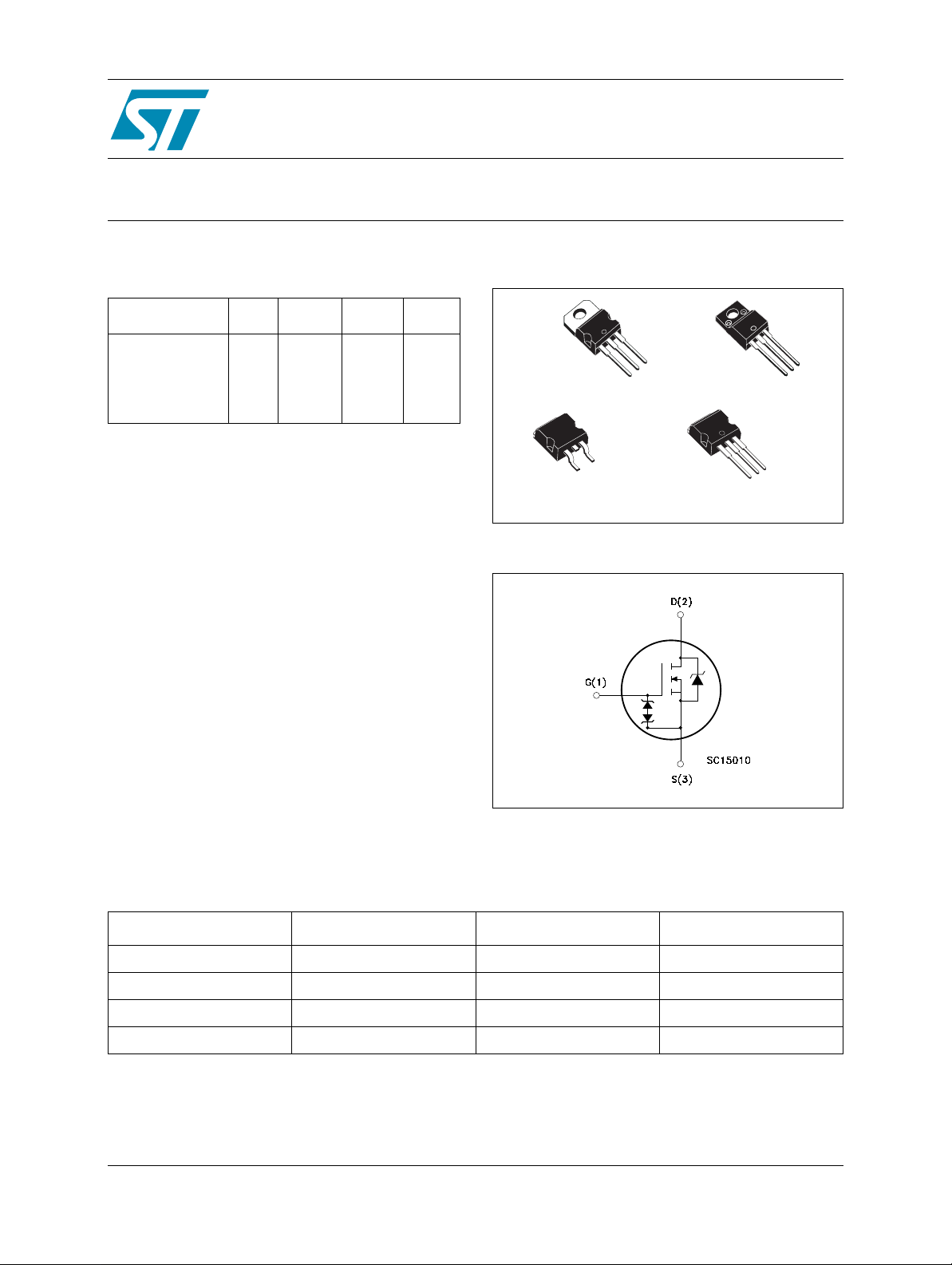
N-CHANNEL 600V - 1Ω - 6A - TO-220/TO-220FP/D²PAK/I²PAK
Zener-Protected SuperMESH™ MOSFET
General features
Type
STB6NK60Z
STB6NK60Z-1
STP6NK60ZFP
STP6NK60Z
■ EXTREMELY HIGH dv/dt CAPABILITY
■ 100% AVALANCHE TESTED
■ GATE CHARGE MINIMIZED
V
DSSRDS(on)
600 V
600 V
600 V
600 V
< 1.2 Ω
< 1.2 Ω
< 1.2 Ω
< 1.2 Ω
I
D
6 A
6 A
6 A
6 A
Pw
110
110
30
110
Description
The SuperMESH™ series is obtained through an
extreme optimization of ST’s well established
strip-based PowerMESH™ layout. In addition to
pushing on-resistance significantly down, spec ial
care is taken to ensure a very good dv/dt
capability for the most demanding applications.
Applications
Package
2
TO-220
1
D²PAK
TO-220FP
1
I²PAK
2
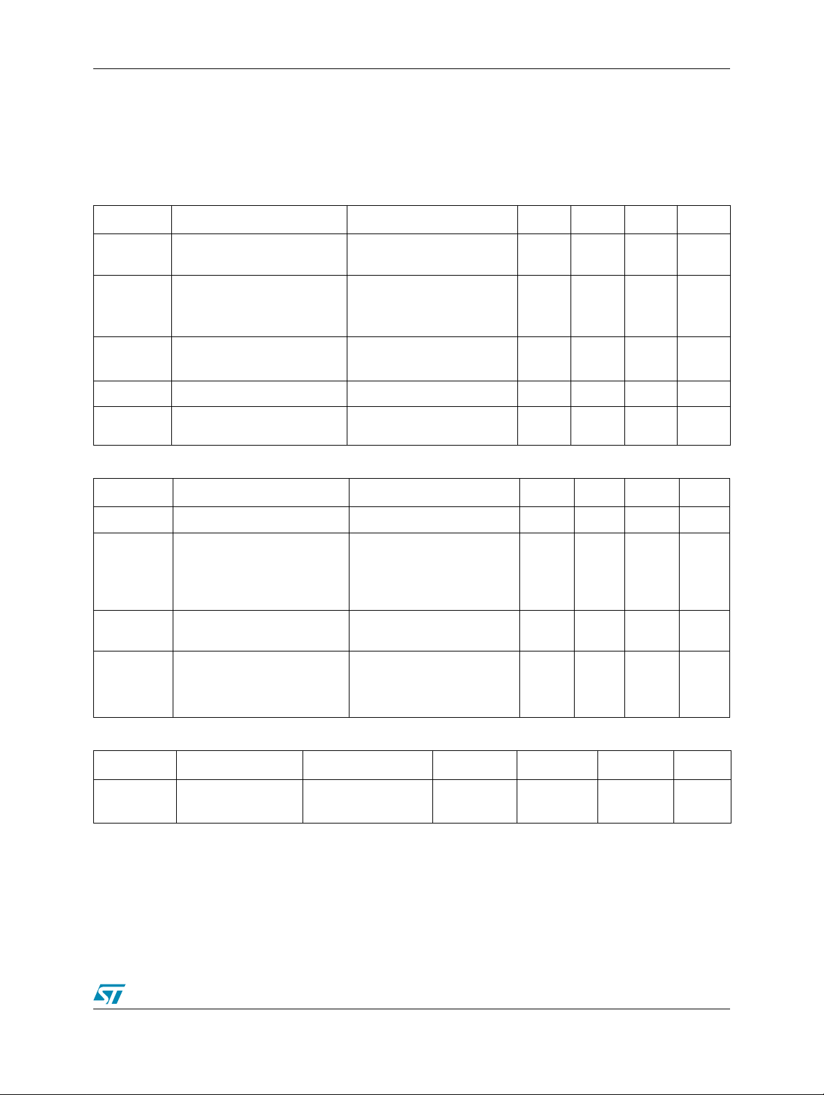
Internal schematic diagram
2
■ HIGH CURRENT, HIGH SPEED SWITCHING
■ IDEAL FOR OFF-LINE POWER SUPPLIES,
ADAPTOR AND PFC
■ LIGHTING
Order codes
Sales Type Marking Package Packaging
STB6NK60Z-1 B6NK60Z-1 I²PAK TUBE
STB6NK60ZT4 B6NK60Z D²PAK TAPE & REEL
STP6NK60ZFP P6NK60ZFP TO-220FP TUBE
STP6NK60Z P6NK60Z TO-220 TUBE
Rev 3
September 2005 1/16
www.st.com
16
Page 2

1 Electrical ratings STB6NK60Z - STB6NK60Z-1 - STP6NK60Z - STP6NK60ZFP
1 Electrical ratings
Table 1. Absolute maximum ratings
Symbol Parameter Value Unit
TO-220/D²/I²PAK TO-220FP
V
DS
V
DGR
V
GS
I
D
I
D
I
DM
Note 1
P
TOT
Drain-Source Voltage (VGS = 0)
Drain-gate Voltage (RGS = 20kΩ)
Gate-Source Voltage ± 30 V
Drain Current (continuous) at TC = 25°C
Drain Current (continuous) at TC = 100°C
Drain Current (pulsed) 24 24 (Note 2) A
Total Dissipation at TC = 25°C
Derating Factor 088 0.24 W/°C
V
ESD(G-S)
dv/dt
Note 3
V
ISO
T
T
stg
G-S ESD (HBM C=100pF, R=1.5kΩ) 3500 V
Peak Diode Recovery voltage slope 4.5 V/ns
Insulation Withstand Volatge (DC) - - 2500 V
Operating Junction Temperature
j
Storage Temperature
Table 2. Thermal data
600 V
600 V
66 (Note 2) A
3.8 3.8 (Note 2) A
110 30 W
-55 to 150 °C
TO-220/I²PAK/D²PAK TO-220FP Unit
Rthj-case Thermal Resistance Junction-case Max 1.14 4.2 °C/W
Rthj-amb Thermal Resist ance Junction-amb Max 62.5 °C/W
T
l
Maximum Lead Temperature For Soldering
Purpose
300 °C
Table 3. Avalanche characteristics
Symbol Parameter Max Valu e Unit
I
AR
E
AS
2/16
Avalanche Curren t, repetitive or
Not-Repetitive (pul se width limited by Tj max)
Single Pulse Avalanche Energy
(starting Tj=25°C, I
D=IAR
, VDD= 50V)
6A
210 mJ
Page 3
STB6NK60Z - STB6NK60Z-1 - STP6NK60Z - STP6NK60ZFP 2 Electrical characteristics
2 Electrical characteristics
(T
= 25 °C unless otherwise specified)
CASE
Table 4. On/Off states
Symbol Parameter Test Conditions Min. Typ. Max. Unit
V
(BR)DSS
I
DSS
I
GSS
V
GS(th)
R
DS(on)
Drain-source
Breakdown Voltage
Zero Gate Voltage
Drain Current (V
GS
= 0)
Gate-body Leakage
Current (V
DS
= 0)
Gate Threshold Voltage
St ati c Drai n-source On
Resistance
= 1 mA, VGS = 0
I
D
V
= Max Rating
DS
= Max Rating, TC = 125
V
DS
°C
= ± 20V
V
GS
= VGS, ID = 100µA
V
DS
V
= 10V, ID = 3 A
GS
600 V
1
50
±10 µA
33.754.5V
11.2Ω
Table 5. Dynamic
Symbol Parameter Test Conditions Min. Typ. Max. Unit
g
fs
Note 4
C
iss
C
oss
C
rss
Forward Tr ansconductance
Input Capacitance
Outp u t C a pacita nce
Rev er se Trans fer Capacita n ce
VDS = 8 V, ID=3 A
= 25V, f = 1 MHz,VGS = 0
V
DS
5S
905
115
25
µA
µA
pF
pF
pF
C
oss eq.
Note 5
Q
g
Q
gs
Q
gd
Equivalent Outp ut
Capacitance
Total Gate Charge
Gate-Source Charge
Gate-Drain Charge
= 0V, VDS = 0V to 480V
V
GS
= 480V, ID = 6 A,
V
DD
V
= 10V
GS
(see Figure 16)
56 pF
33
6
46
17
Table 6. Gate-source zener diode
Symbol Parameter T est Conditions Min. Ty p. Max. Unit
BV
GSO
Note 6
Gate-Source
Breakdown Voltage
Igs=±1mA
(Open Drain)
30 V
nC
nC
nC
3/16
Page 4
2 Electrical characteristics STB6NK60Z - STB6NK60Z-1 - STP6NK60Z - STP6NK60ZFP
Table 7. Switching times
Symbol Parameter Test Conditions Min. Typ. Max. Unit
= 300 V, ID = 3 A
V
t
d(on)
Tur n-on Delay Time
t
r
Rise Time
DD
R
=4.7Ω VGS = 10 V
G
(see Figure 15)
14
14
ns
ns
t
d(off)
t
t
r(Voff)
t
t
Turn-off Delay Time
f
Fall Ti me
Off-vol tage Rise Tim e
f
c
Fall Ti me
Cross-over T ime
= 300 V, ID = 3 A
V
DD
R
=4.7Ω VGS = 10 V
G
(see Figure 15)
= 480V, ID = 6 A,
V
DD
R
=4.7Ω, V
G
GS
(see Figure 15)
= 10V
47
19
16
16
29
Table 8. Source drain diode
Symbol Parameter Test Conditions Min. Typ. Max. Unit
I
SD
I
Note 1
SDM
V
Note 4
SD
t
rr
Q
rr
I
RRM
(1) Pul s e width limited by safe operating area
(2)Limi ted only by maximum temperature allowed
≤6A, di/dt ≤200A/µs, VDD=80% V
(3) I
SD
(4) Pulsed: pulse duration = 300µs, duty cycle 1.5%
(5) C
oss eq.
to 80%
(6) The built-in back-to-back Zener diodes have specifically been designed to enhance not only the device’s ESD capability,
but also to make them safely absorb possible voltage transients that may occasionally be applied from gate to source. In
this respect the Zener voltage is approp riate t o achieve an effi cient and cost-effecti ve interv ention to protect the devi ce’s
integrity. These integrated Zener diodes thus avoid the usage of external components
Source-drain Current
Source-drain Current (pulsed)
Forward On Voltage
Reverse Recovery Time
Reverse Recovery Charge
Reverse Recovery Current
(BR)DSS
is defined as a constant equivalent capacitance giving the same charging time as C
ISD = 6 A, VGS = 0
= 6 A, di/dt = 100A /µs
I
SD
V
= 50 V, Tj = 150°C
DD
(see Figure 17)
.
6
24
1.6 V
445
2.7
12
when VDS increases from 0
oss
ns
ns
ns
ns
ns
A
A
ns
µC
A
4/16
Page 5

STB6NK60Z - STB6NK60Z-1 - STP6NK60Z - STP6NK60ZFP 2 Electrical characteristics
2.1 Elect rical character i st ic s (curves)
Figure 1. Safe Operat in g Are a f or
TO-220/D²/I²PAK
Figure 3. Safe Operating Area for TO-220FP Figure 4. Therm al Impedan ce for TO-220FP
Figure 2. Therm al Impedanc for
TO-220/D²/I²PAK
Figure 5. Output Characteristics Figure 6. Transfer Characteristics
5/16
Page 6

2 Electrical characteristics STB6NK60Z - STB6NK60Z-1 - STP6NK60Z - STP6NK60ZFP
Figure 7. Transconductance Figure 8. Static Drain-Source on Resistance
Figure 9. Gate Charge vs Gate -Source
Voltage
Figure 11. Normali z ed Gate Threshold Voltage
vs Temperatute
Figure 10. Capacitance Variations
Figure 12. Normalized on Resistance vs
Temperature
6/16
Page 7

STB6NK60Z - STB6NK60Z-1 - STP6NK60Z - STP6NK60ZFP 2 Electrical characteristics
Figure 13. Source-drain Diode Forward
Characteristics
Figure 14. Normalized BVDSS vs Temperature
7/16
Page 8

3 Test circuits STB6NK60Z - STB6NK60Z-1 - STP6NK60Z - STP6NK60ZFP
3 Test circuits
Figure 15. Switching Times Test Circuit For
Resistive Load
Figure 17. Test Circuit For Inductive Load
Switching and Diode Recovery
Times
Figure 16. Gate Charge Test Circuit
8/16
Page 9

STB6NK60Z - STB6NK60Z-1 - STP6NK60Z - STP6NK60ZFP 4 Package mechanical data
4 P ack age mechanical data
In order to meet environmental requirements, ST offers these devices in ECOPACK®
packages. These packages have a Lead-free second level interconnect . The category of
second level interconnect is marked on the package and on the inner box label, in compliance
with JEDEC Standard JESD97. The maximum ratings related to soldering conditions are also
marked on the inner box label. ECOPACK is an ST trademark. ECOP ACK specifications are
available at: www.st.com
9/16
Page 10

4 Package mechanical data STB6NK60Z - STB6NK60Z-1 - STP6NK60Z - STP6NK60ZFP
TO-220 MECHANICAL DATA
DIM.
A 4.40 4.60 0.173 0.181
b 0.61 0.88 0.024 0.034
b1 1.15 1.70 0.045 0.066
c 0.49 0.70 0.019 0.027
D 15.25 15.75 0.60 0.620
E 10 10.40 0.393 0.409
e 2.40 2.70 0.094 0.106
e1 4.95 5.15 0.194 0.202
F 1.23 1.32 0.048 0.052
H1 6.20 6.60 0.244 0.256
J1 2.40 2.72 0.094 0.107
L 13 14 0.511 0.551
L1 3.50 3.93 0.137 0.154
L20 16.40 0.645
L30 28.90 1.137
øP 3.75 3.85 0.147 0.151
Q 2.65 2.95 0.104 0.116
MIN. TYP MAX. MIN. TYP. MAX.
mm. inch
10/16
Page 11

STB6NK60Z - STB6NK60Z-1 - STP6NK60Z - STP6NK60ZFP 4 Package mechanical data
D2PAK MECHANICAL DATA
TO-247 MECHANICAL DATA
TO-220FP MECHANICAL DATA
DIM.
DIM.
A 4.4 4.6 0.173 0.181
A 4.4 4.6 0.173 0.181
A1 2.49 2.69 0.098 0.106
B 2.5 2.7 0.098 0.106
D 2.5 2.75 0.098 0.108
A2 0.03 0.23 0.001 0.009
E 0.45 0.7 0.017 0.027
B 0.7 0.93 0.027 0.036
F 0.75 1 0.030 0.039
B2 1.14 1.7 0.044 0.067
F1 1.15 1.7 0.045 0.067
C 0.45 0.6 0.017 0.023
F2 1.15 1.7 0.045 0.067
G 4.95 5.2 0.195 0.204
C2 1.23 1.36 0.048 0.053
G1 2.4 2.7 0.094 0.106
D 8.95 9.35 0.352 0.368
H 10 10.4 0.393 0.409
D1 8 0.315
L2 16 0.630
E 10 10.4 0.393
L3 28.6 30.6 1.126 1.204
E1 8.5 0.334
L4 9.8 10.6 .0385 0.417
L5 2.9 3.6 0.114 0.141
G 4.88 5.28 0.192 0.208
L6 15.9 16.4 0.626 0.645
L 15 15.85 0.590 0.625
L7 9 9.3 0.354 0.366
L2 1.27 1.4 0.050 0.055
Ø 3 3.2 0.118 0.126
L3 1.4 1.75 0.055 0.068
M 2.4 3.2 0.094 0.126
R0.4 0.015
V2 0º 4º
A
MIN. TYP MAX. MIN. TYP. MAX.
MIN. TYP MAX. MIN. TYP. MAX.
mm. inch
mm. inch
E
D
B
L3
L6
L7
F1
F
G1
H
F2
L2
3
L5
123
L4
G
1
11/16
Page 12

4 Package mechanical data STB6NK60Z - STB6NK60Z-1 - STP6NK60Z - STP6NK60ZFP
TO-262 (I2PAK) MECHANICAL DATA
DIM.
A 4.40 4.60 0.173 0.181
A1 2.40 2.72 0.094 0.107
b 0.61 0.88 0.024 0.034
b1 1.14 1.70 0.044 0.066
c 0.49 0.70 0.019 0.027
c2 1.23 1.32 0.048 0.052
D 8.95 9.35 0.352 0.368
e 2.40 2.70 0.094 0.106
e1 4.95 5.15 0.194 0.202
E 10 10.40 0.393 0.410
L 13 14 0.511 0.551
L1 3.50 3.93 0.137 0.154
L2 1.27 1.40 0.050 0.055
MIN. TYP MAX. MIN. TYP. MAX.
mm. inch
12/16
Page 13

STB6NK60Z - STB6NK60Z-1 - STP6NK60Z - STP6NK60ZFP 4 Package mechanical data
D2PAK MECHANICAL DATA
TO-247 MECHANICAL DATA
DIM.
A 4.4 4.6 0.173 0.181
A1 2.49 2.69 0.098 0.106
A2 0.03 0.23 0.001 0.009
B 0.7 0.93 0.027 0.036
B2 1.14 1.7 0.044 0.067
C 0.45 0.6 0.017 0.023
C2 1.23 1.36 0.048 0.053
D 8.95 9.35 0.352 0.368
D1 8 0.315
E 10 10.4 0.393
E1 8.5 0.334
G 4.88 5.28 0.192 0.208
L 15 15.85 0.590 0.625
L2 1.27 1.4 0.050 0.055
L3 1.4 1.75 0.055 0.068
M 2.4 3.2 0.094 0.126
R0.4 0.015
V2 0º 4º
MIN. TYP MAX. MIN. TYP. MAX.
mm. inch
3
1
13/16
Page 14

5 Packing mechanical data STB6NK60Z - STB6NK60Z-1 - STP6NK60Z - STP6NK60ZFP
5 Packing mechanical data
D2PAK FOOTPRINT
TAPE AND REEL SHIPMENT
REEL MECHANICAL DATA
DIM.
A 330 12.992
B 1.5 0.059
C 12.8 13.2 0.504 0.520
D 20.2 0795
G 24.4 26.4 0.960 1.039
N 100 3. 937
T 30.4 1.197
mm inch
MIN. MAX . MIN. MAX.
T APE MECHANICAL DATA
DIM.
A0 10.5 10.7 0.413 0.421
B0 15.7 15.9 0.618 0.626
D 1.5 1.6 0.059 0.063
D1 1.59 1.61 0.062 0.063
E 1.65 1.85 0.065 0.073
F 11.4 11.6 0.449 0.456
K0 4.8 5.0 0.189 0.197
P0 3.9 4.1 0.153 0.161
P1 11.9 12.1 0.468 0.476
P2 1.9 2.1 0.075 0.082
R 50 1.574
T 0.25 0.35 0.0098 0.0137
W 23.7 24.3 0.933 0.956
* on sales type
mm inch
MIN. MAX. MIN. MAX.
14/16
BASE QTY BULK QTY
1000 1000
Page 15

STB6NK60Z - STB6NK60Z-1 - STP6NK60Z - STP6NK60ZFP 6 Revision History
6 R evi sion History
Date Revision Changes
05-Aug-2005 2 Inserted Ecopack indication
28-Sep-2005 3 Modified header
15/16
Page 16

6 Revision History STB6NK60Z - STB6NK60Z-1 - STP6NK60Z - STP6NK60ZFP
I
s
o
d
b
ct
t
ot
a
nformation furnished is believed to be accurate and reliable. However, STMicroelectronics assumes no responsibility for the consequence
f use of such information nor for any infringement of patents or other rights of third parties which may result from its use. No license is grante
y implic ation or oth erwise under any patent or pat ent rights of STMicroelectron i cs. Specific ations me nt i oned in thi s publication are s ubje
o change without notice. This publication supersedes and replaces all information previously supplied. STMicroelectronics products are n
uthoriz ed for use as crit ic al component s i n l i fe support devic es or systems wi thout express written appr oval of STMicroelectron ics.
The ST logo is a registered trademark of ST M i croelectr onics.
All other nam es are the pro perty of their respective owners
Austra l i a - Be l gi um - Brazil - C anada - China - Czech Republic - Finland - F rance - Germany - Hong Kon g - India - Israe l - It al y - Japan -
Malaysi a - M al ta - Morocco - Singapore - Spain - Swede n - Switzerland - United Kingdom - United States of America
© 2005 STMi croelectro ni cs - All rights reserved
STMicroelectronic s group of companies
www.st.com
16/16
 Loading...