

STMicroelectronics STD4NK50ZD, STD4NK50ZD-1, STF4NK50ZD, STP4NK50ZD Technical data
STD4NK50ZD - STD4NK50ZD-1
1
3
3
3
1
3
STF4NK50 ZD - STP4NK50ZD
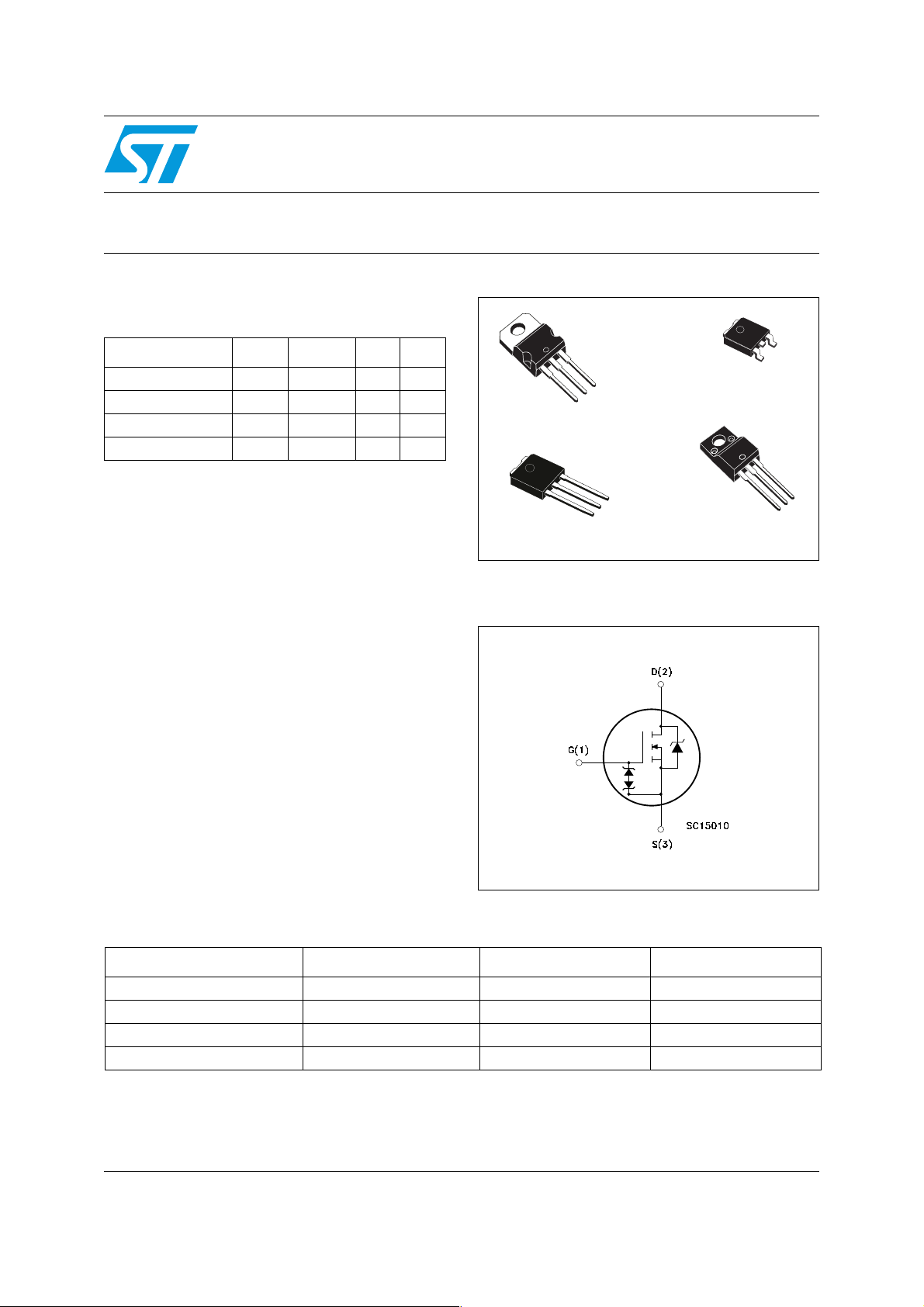
N-channel 500V - 2.4Ω - 3A - TO-220 - TO-220FP- DPAK - IPAK
Fast diode SuperMESH™ Power MOSFET
General features
Type V
STD4NK50ZD-1 500V <2.7Ω 3A 45W
STD4NK50ZD 500V <2.7Ω 3A 45W
STF4NK50ZD 500V <2.7Ω 3A 20W
STP4NK50ZD 500V <2.7Ω 3A 45W
■ 100% avalanche tested
■ Extremely high dv/dt capability
■ Gate charge minimized
■ Very low intrinsic capacitances
■ Very good manufacturing repeability
DSS
R
DS(on)ID
Pw
TO-220
IPAK
2
2
1
DPAK
TO-220FP
1
2
Description
The fast SuperMESH™ series as sociate s all
advantages of reduced on-resistance, zener gate
protection and outstanding dc/dt capability with a
Fast body-drain recovery diode. Such series
complements the FDmesh™ advanced tecnology.
Applications
■ Switching application
Order codes
Part number Marking Package Packaging
STD4NK50ZD-1 D4NK50ZD-1 IPAK Tube
STD4NK50ZD D4NK50ZD DPAK Tape & reel
STF4NK50ZD F4NK50ZD TO-220FP Tube
STP4NK50ZD P4NK50ZD TO-220 Tube
Internal schematic diagram
April 2006 Rev 3 1/17
www.st.com
17

Contents STD4NK50ZD - STD4NK50ZD-1 - STF4NK50ZD - STP4NK50ZD
Contents
1 Electrical ratings . . . . . . . . . . . . . . . . . . . . . . . . . . . . . . . . . . . . . . . . . . . . 3
2 Electrical characteristics . . . . . . . . . . . . . . . . . . . . . . . . . . . . . . . . . . . . . 5
2.1 Electrical characteristics (curves) . . . . . . . . . . . . . . . . . . . . . . . . . . . . 6
3 Test circuit . . . . . . . . . . . . . . . . . . . . . . . . . . . . . . . . . . . . . . . . . . . . . . . 10
4 Package mechanical data . . . . . . . . . . . . . . . . . . . . . . . . . . . . . . . . . . . . 11
5 Packaging mechanical data . . . . . . . . . . . . . . . . . . . . . . . . . . . . . . . . . . 16
6 Revision history . . . . . . . . . . . . . . . . . . . . . . . . . . . . . . . . . . . . . . . . . . . 17
2/17
STD4NK50ZD - STD4NK50ZD-1 - STF4NK50ZD - STP4NK50ZD Electrical ratings
1 Electrical ratings
Table 1. Abs olute maxim um ratings
Value
Symbol Parameter
TO-220 IPAK/DPAK TO-220FP
Unit
V
I
P
V
DGR
V
I
I
DM
TOT
Drain-source voltage (VGS = 0) 500 V
DS
Drain-gate voltage (RGS = 20KΩ) 500 V
Gate-source voltage ± 30 V
GS
Drain current (continuous) at TC = 25°C 3
D
Drain current (continuous) at TC=100°C 1.9
D
(2)
Drain current (pulsed) 12
Total dissipation at TC = 25°C 45 20 W
Derating factor 0.36 0.16 W/°C
V
ESD(G-D)
dv/dt
V
T
T
1. Limited only by max im um temper a tu r e all ow e d
2. Pulse width limited by safe operating area
3. ISD ≤3A, di/dt ≤200A/µs, VDD =80%V
Gate source ESD(HBM-C=100pF, R=1.5KΩ) 2800 V
(3)
Peak diode recovery voltage slope 15 V/ns
Insulation withstand voltage (DC) -- -- 2500 V
ISO
Operating junction temperature
J
Storage temperature
stg
(BR)DSS
Table 2. Th erm al resi stance
3
1.9
12
(1)
(1)
(1)
3
1.9
12
(1)
(1)
(1)
-55 to 150 °C
A
A
A
Value
Symbol Parameter
TO-220 IPAK/DPAK TO-220FP
R
thj-case
R
thj-a
T
Thermal resistance junction-case Max 2.78 6.25 °C/W
Thermal resistance junction-ambient Max 62.5 100 62.5 °C/W
Maximum lead tempera ture for soldering
l
purpose
300 °C
Table 3. Avalanche data
Symbol Parameter Value Unit
I
AR
E
AS
Avalanche current, repetitive or not-repetiti ve
(pulse width limited by Tj Max)
Single pulse avalanche energy
(starting Tj=25°C, Id=Iar, Vdd=50V)
3A
120 mJ
Unit
3/17

Electrical characteristics STD4NK50ZD - STD4NK50ZD-1 - STF4NK50ZD - STP4NK50ZD
2 Electrical characteristics
(T
=25°C unless otherwise specified)
CASE
Table 4. On /off states
Symbol Parameter T est condictions Min. T yp. Max. Unit
V
(BR)DSS
I
DSS
I
GSS
V
GS(th)
R
DS(on)
Drain-source breakdown
voltage
Zero gate voltage drain
current (V
GS
= 0)
Gate body leakage curren t
= 0)
(V
DS
Gate threshold voltage
Sta ti c drain-source on
resistance
I
= 1mA, VGS= 0
D
V
= Max rating,
DS
= Max rating @125°C
V
DS
= ±20V
V
GS
V
= VGS, ID = 50µA
DS
V
= 10V, ID= 1.5A
GS
500 V
1
50
±10 µA
2.5 3.5 4.5 V
2.3 2.7 Ω
Table 5. Dyn amic
Symbol Parameter Test condictions Min. Typ. Max. Unit
C
oss eq
(1)
g
fs
C
C
C
Forward transconductance
Input capacitance
iss
Output capacitance
oss
Reverse transfe r
rss
capacitance
(2)
Equivalent output
.
capacitance
=15V, ID = 1.5A
V
DS
= 25V, f = 1 MHz,
V
DS
V
= 0
GS
V
= 0, V
GS
DS
=0V to 400V
1.5 S
310
49
10
33 pF
µA
µA
pF
pF
pF
Q
g
Total gate charge
Q
Q
1. Pulsed: pulse duration=300 µs, duty cycle 1.5%
2. C
inceases from 0 to 80% V
Gate-source charge
gs
Gate-drain char ge
gd
is def ined as a constant eq uivalent capacitance gi ving the same charging time as C
oss eq.
DSS
V
V
(see Figure 11)
Table 6. Swi tching times
Symbol Pa rameter Test condictions Min. T yp. Max. Unit
t
d(on)
t
d(off)
4/17
Turn-on delay time
t
Rise time
r
Turn-off del ay tim e
Fall time
t
f
V
R
(see Figure 18)
= 400V, ID = 3A
DD
=10V
GS
= 250 V, ID= 1.5A,
DD
= 4.7Ω, V
G
GS
=10V
12
3
7
9.5
15.5
23
22
when VDS
oss
nC
nC
nC
ns
ns
ns
ns

STD4NK50ZD - STD4NK50ZD-1 - STF4NK50ZD - STP4NK50ZD Electrical characteristics
Table 7. S ource drain diode
Symbol Parameter Test condictions Min Typ. Max Unit
I
SD
I
SDM
V
SD
t
Q
I
RRM
t
Q
I
RRM
1. Pulse width limited by safe operating area
2. Pulsed: pulse duration=300 µs, duty cycle 1.5%
Source -drain current 3 A
(1)
Source-drain current (pulsed) 12 A
(2)
Forward on voltage
rr
Reverse rec overy time
Reverse recovery charge
rr
Reverse rec overy current
rr
Reverse rec overy time
Reverse Recovery Char ge
rr
Reverse rec overy current
= 3A, VGS=0
I
SD
= 3A,
I
SD
di/dt = 100A/µs,
= 34V, Tj = 25°C
V
DD
= 3A,
I
SD
di/dt = 100A/µs,
= 34V, Tj = 150°C
V
DD
73
140
3.82
118
260
4.4
1.6 V
Table 8. Gate-source zen er di ode
Symbol Parameter Test condictions Min. Typ. Max Unit
Gate-source braekdown
(1)
BV
GSO
1. The bui lt-in b ack-to-back Zener diodes have specifically been designed to enhance not onl y the device’s
ESD capability, but also to make them safely absorb possible voltage transients that may occasionally be
applied from gate to source. In this respect the Zener voltage is appropriate to achieve an efficient and
cost-effective intervention to protect the device’s integrity. These integrated Zener diodes thus avoid the
usage of ex te r na l co mp on ents.
voltage
= ±1mA (open drain) 30 V
I
GS
ns
nC
A
ns
nC
A
5/17
Electrical characteristics STD4NK50ZD - STD4NK50ZD-1 - STF4NK50ZD - STP4NK50ZD
2.1 Electrical characteristics (curves)
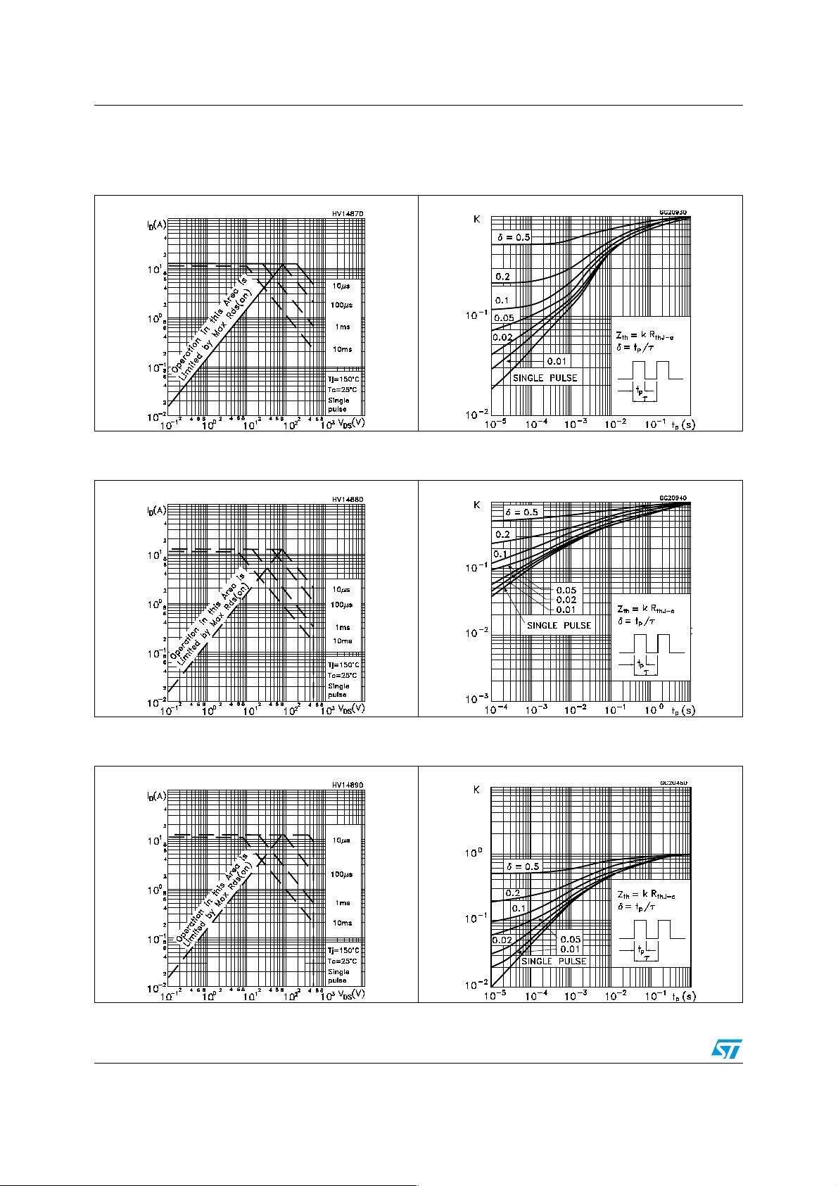
Figure 1. Safe operating area for TO-220 Figure 2. Thermal impedance for TO-220
Figure 3. Safe operating areafor TO-220FP Figure 4. Thermal impedance for TO-220FP
Figure 5. Safe operating area for DPAK/IPAK Figure 6. Thermal impedance for DPAK/IPAK
6/17
 Loading...