

STMicroelectronics STP45NF06, STB45NF06 Technical data
STP45NF06
STB45NF06
N-CHANNEL 60V - 0.022Ω - 38A TO-220/D2PAK
STripFET™II MOSFET
Table 1: Ge neral Features
TYPE V
STP45NF06
STB45NF06
■ TYPICAL R
■ EXCEPTIONAL dv/dt CAPABILITY
■ STANDARD THRESHOLD DRIVE
■ 100% AVALANCHE TESTED
DSS
60 V
60 V
(on) = 0.022Ω
DS
R
DS(on)
< 0.028 Ω
< 0.028 Ω
I
D
38 A
38 A
DESCRIPTION
This MOSFET is th e latest developm ent of STM icroelectronics unique “Single Feature Size™”
strip-based process. The resulting transistor
shows extremely high pac king density for low onresistance, rugged avalance characteristics and
less critical alignment steps therefore a remarkable manufacturing reproducibility.
APPLICATIONS
■ HIGH-EFFICIENCY DC-DC CONVERTERS
■ SOLENOID AND RELAY DRIVERS
■ DC-DC & DC-AC CONVERTERS
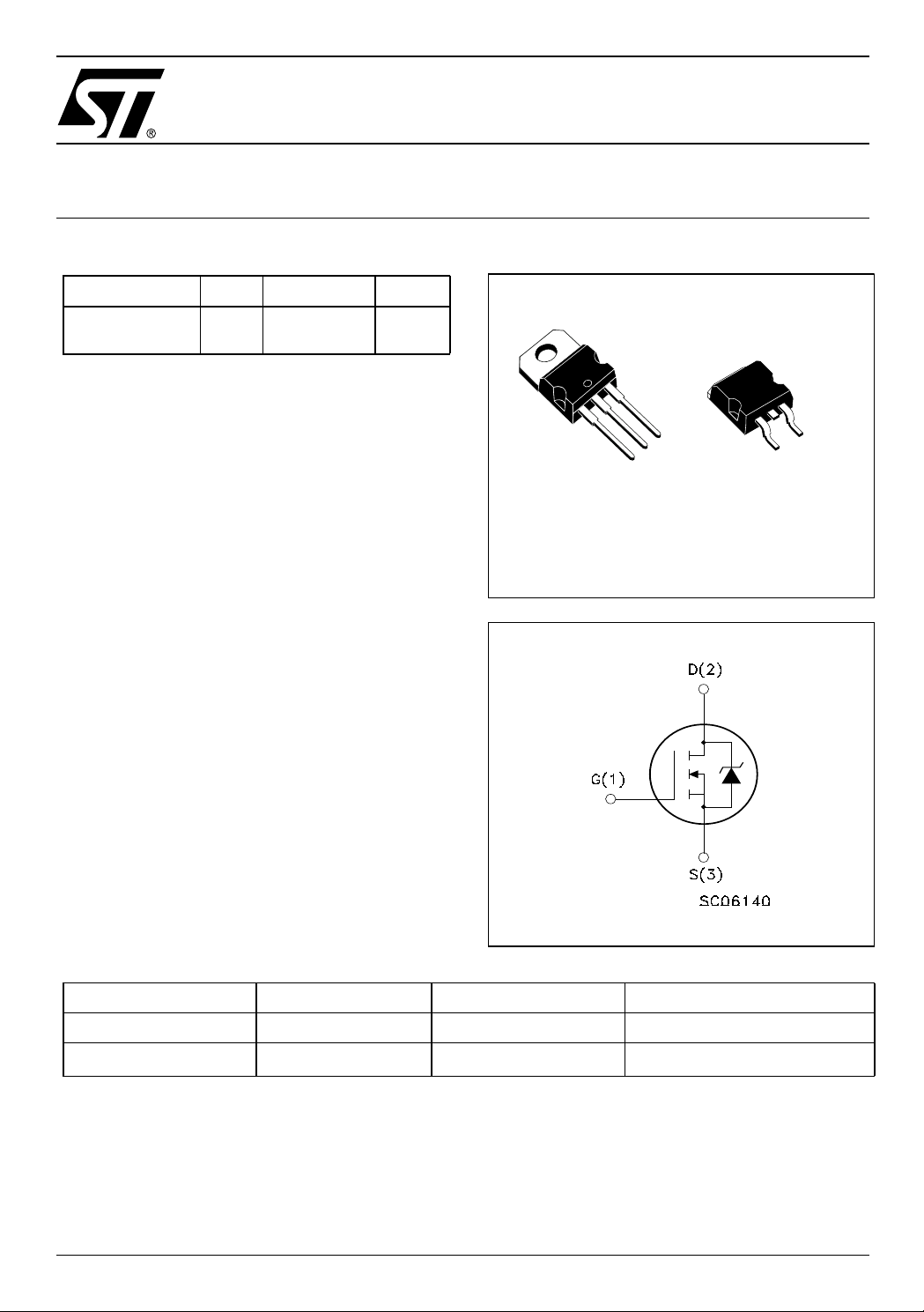
Figure 1: Package
TO-220
3
2
1
1
D2PAK
Figure 2: Internal Schematic Diagram
3
Table 2: Order Codes
SALES TYPE MARKING PACKAGE PACKAGING
STP45NF06 P45NF06 TO-220 TUBE
STB45NF06T4 B45NF06
2
D
PAK
TAPE & REEL
Rev. 2
1/11June 2004
STP45NF06 - STB45NF06
Table 3: Absolute Maximum ratings
Symbol Parameter Value Unit
V
DS
V
DGR
V
GS
I
D
I
D
I
DM
P
TOT
dv/dt (1) Peak Diode Recovery voltage slope 7 V/ns
T
stg
T
() Pulse wi dt h l i m i ted by safe opera ting area
≤ 38A, di/dt ≤ 300A/µs, VDD ≤ V
(1) I
SD
Table 4: Thermal Data
Rthj-case Thermal Resistance Junction-case Max 1.87 °C/W
Rthj-amb Thermal Resistance Junction-ambient Max 62.5 °C/W
T
Drain-source Voltage (VGS = 0)
Drain-gate Voltage (RGS = 20 kΩ)
60 V
60 V
Gate- source Voltage ±20 V
Drain Current (continuous) at TC = 25°C
Drain Current (continuous) at TC = 100°C
()
Drain Current (pulsed) 152 A
Total Dissipation at TC = 25°C
38 A
26 A
80 W
Derating Factor 0.53 W/°C
Storage Temperature –65 to 175 °C
Max. Operating Junction Temperature 175 °C
j
, Tj ≤ T
(BR)DSS
Maximum Lead Temperature For Soldering Purpose 300 °C
l
JMAX.
Table 5: Avalanche Characteristics
Symbol Parameter Max Value Unit
I
AR
E
AS
Avalanche Current, Repetitive or Not-Repetitive
(pulse width limited by T
max)
j
Single Pulse Avalanche Energy
(starting T
= 25 °C, ID = IAR, VDD = 50 V)
j
ELECTRICAL CHARACTERISTICS (T
=25°C UNLESS OTHERWISE SPECIFIED)
CASE
38 A
135 mJ
Table 6: Off
Symbol Parameter Test Conditions Min. Typ. Max. Unit
V
(BR)DSS
Drain-source
ID = 250 µA, VGS = 0 60 V
Breakdown Voltage
I
DSS
I
GSS
Zero Gate Voltage
Drain Current (V
GS
Gate-body Leaka ge
Current (V
DS
= 0)
= 0)
= Max Rating
V
DS
V
= Max Rating, TC= 125°C
DS
V
= ±20V ±100 nA
GS
1
10
Table 7: On
Symbol Parameter Test Conditions Min. Typ. Max. Unit
V
V
GS(th)
R
DS(on)
Gate Threshold Voltage
Static Drain-source On
Resistance
= VGS, ID = 250µA
DS
234V
VGS = 10 V, ID = 19 A 0.022 0.028 Ω
µA
µA
2/11
STP45NF06 - STB45NF06
ELECTRICAL CHARACTERISTICS (CONTINUED)
Table 8: Dynamic
Symbol Parameter Test Conditions Min. Typ. Max. Unit
(1) Forward Transconductance VDS > I
g
fs
C
iss
C
oss
C
rss
Input Capacitance
Output Capacitance
Reverse Transfer
Capacitance
I
D
V
=19 A
DS
Table 9: Switching On
Symbol Parameter Test Conditions Min. Typ. Max. Unit
t
d(on)
t
r
Q
g
Q
gs
Q
gd
Table 10: Switching Off
Turn-on Delay Time
Rise Time 100 ns
Total Gate Charge
Gate-Source Charge
Gate-Drain Charge
Symbol Parameter Test Conditions Min. Typ. Max. Unit
t
d(off)
t
f
t
d(off)
t
f
t
c
Table 11: Source Drain Diode
Turn-off-Delay Time
Fall Time
Off-voltage Rise Time
Fall Time
Cross-over Time
Symbol Parameter Test Conditions Min. Typ. Max. Unit
I
SD
I
SDM
VSD (2)
t
rr
Q
rr
I
RRM
(1) Pulsed: Pulse durat i on = 300 µs, du t y cy cle 1.5 %.
(2) Pulse width limite d by safe operating area.
Source-drain Current 38 A
(1)
Source-drain Current (pulsed) 152 A
Forward On Voltage
Reverse Recovery Time
Reverse Recovery Charge
Reverse Recovery Current
V
DD
R
=4.7Ω VGS = 10V
G
(see test circuit, Figure 3)
VDD = 48V, ID = 38A,
VGS = 10V
VDD = 30V, ID = 19A,
R
=4.7Ω, V
G
(see test circuit, Figure 3)
Vclamp =48V, ID =38A
RG=4.7Ω, V
(see test circuit, Figure 5)
ISD = 38A, VGS = 0
= 38A, di/dt = 100A/µs,
I
SD
VDD = 100V, Tj = 150°C
(see test circuit, Figure 5)
D(on)
x R
DS(on)max,
24 S
= 25V, f= 1 MHz, VGS= 0 1730
215
63
= 30V, ID = 19A
20 ns
43
9
15
50
GS
= 10V
20
45
GS
= 10V
42
60
95
260
5.5
58 nC
1.5 V
pF
pF
pF
nC
nC
ns
ns
ns
ns
ns
ns
nC
A
3/11
STP45NF06 - STB45NF06
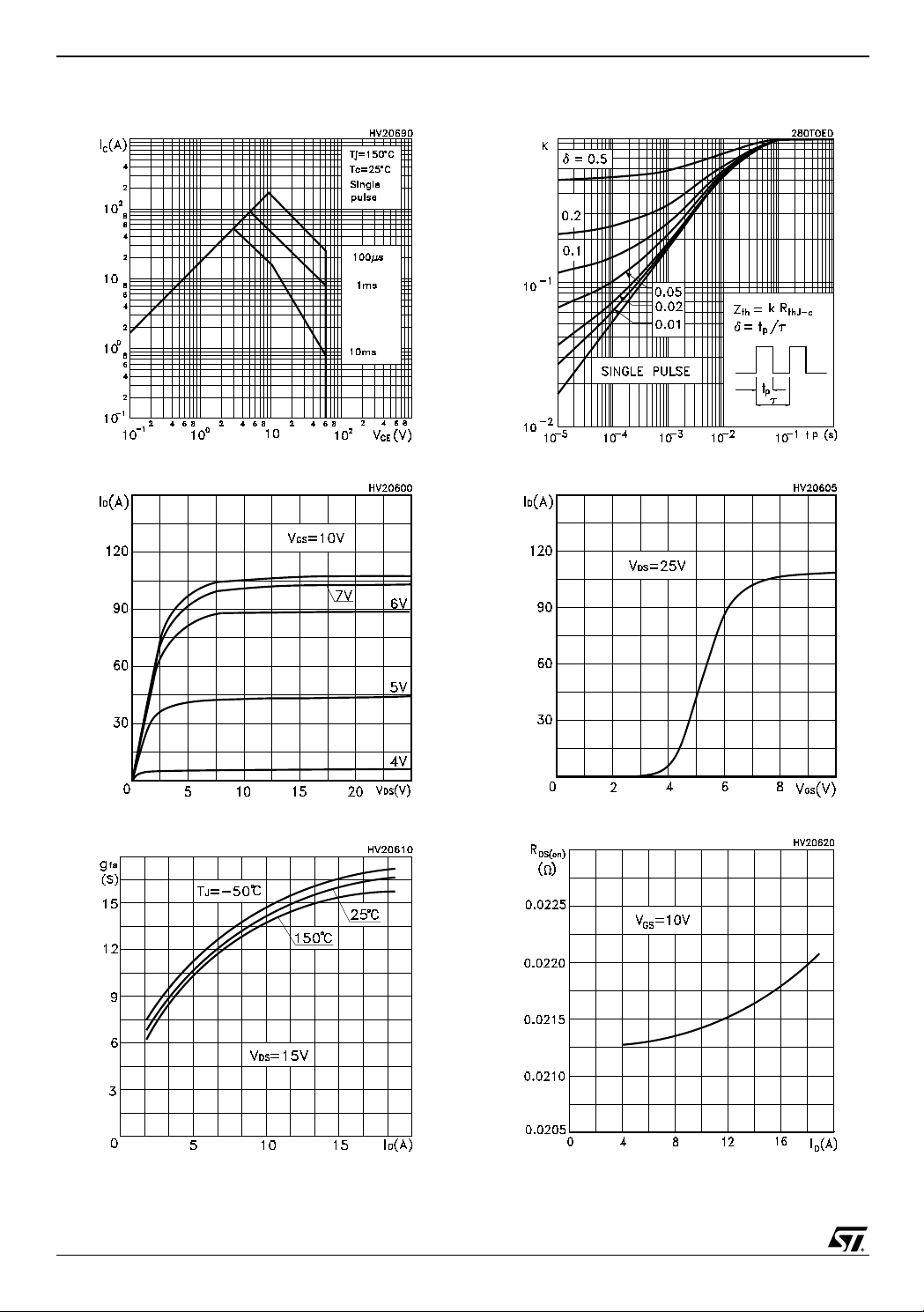
Figure 3: Safe Operating Area
Figure 4: Output Characteristics
Figure 6: Thermal Impedance
Figure 7: Transfer Characteristics
Figure 5: Transconductance
4/11
Figure 8: Static Drain-source On Resistance
 Loading...