

STMicroelectronics STP20N20, STF20N20 Technical data
STP20N20
STF20N20 - STD20N20
N-CHANNEL 200V - 0.10Ω - 18A TO-220/TO-220FP/DPAK
LOW GATE CHARGE STripFET™ II MOSFET
Table 1: Ge neral Features
TYPE V
STD20N20
STF20N20
STP20N20
■ TYPICAL R
■ EXCEPTIONAL dv/dt CAPABILITY
■ LOW GATE CHARGE
■ 100% AVALANCHE TESTED
DSS
200 V
200 V
200 V
(on) = 0.10 Ω
DS
R
DS(on)
< 0.125 Ω
< 0.125 Ω
< 0.125 Ω
I
d
18 A
18 A
18 A
P
TOT
90 W
25 W
90 W
DESCRIPTION
This MOSFET series realized with STMicroelectronics unique S TripFET process has specifically
been designed to minim ize i nput c apacitance a nd
gate charge. It is therefore suitable as primary
switch in advanced high-efficiency isolated DC-DC
converters.
APPLICATIONS
■ HIGH CURRENT SWITCHING
APPLICATIONS
■ HIGH EFFICIENCY DC-DC CONVERTERS
■ PRIMARY SIDE SWITCH
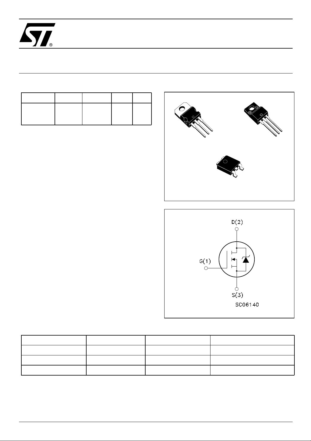
Figure 1: Package
3
2
1
TO-220
TO-220FP
3
1
DPAK
Figure 2: Internal Schematic Diagram
3
2
1
Table 2: Order Codes
SALES TYPE MARKING PACKAGE PACKAGING
STD20N20T4 D20N20 DPAK TAPE & REEL
STF20N20 F20N20 TO-220FP TUBE
STP20N20 P20N20 TO-220 TUBE
Rev. 3
1/13January 2005
STP20N20 - STF20N20 - STD20N20
Table 3: Absolute Maximum ratings
Symbol Parameter Value Unit
TO-220/DPAK TO-220FP
V
DS
V
DGR
V
GS
I
D
I
D
I
DM
P
TOT
dv/dt (1) Peak Diode Recovery voltage slope 15 V/ns
T
j
T
stg
() Pulse wi dt h l i m i ted by safe operating area
(1) I
≤ 18A, di/dt ≤ 400A/µs, VDD ≤ V
SD
Table 4: Thermal Data
Rthj-case Thermal Resistance Junction-case Max 1.38 1.38 5 °C/W
Rthj-amb Thermal Resistance Junction-ambient Max 62.5 50(#) 62.5 °C/W
T
l
(#) When mounted on 1inch² FR-4, 2 Oz copper board.
Drain-source Voltage (VGS = 0) 200 V
Drain-gate Voltage (RGS = 20 kΩ)200V
Gate- source Voltage
± 20 V
Drain Current (continuous) at TC = 25°C18A
Drain Current (continuous) at TC = 100°C11A
()
Drain Current (pulsed)
72 A
Total Dissipation at TC = 25°C9025W
Derating Factor 0.72 0.2 W/°C
Operating Junction Temperature
Storage Temperature
(BR)DSS
-50 to 150 °C
TO-220 DPAK TO-220FP
Maximum Lead Temperature For Soldering
300 °C
Purpose
Table 5: Avalanche Characteristics
Symbol Parameter Max Value Unit
I
AR
E
AS
Avalanche Current, Repetitive or Not-Repetitive
(pulse width limited by T
max)
j
Single Pulse Avalanche Energy
(starting T
= 25 °C, ID = IAR, VDD = 50 V)
j
ELECTRICAL CHARACTERISTICS (T
=25°C UNLESS OTHERWISE SPECIFIED)
CASE
18 A
110 mJ
Table 6: On/Off
Symbol Parameter Test Conditions Min. Typ. Max. Unit
V
(BR)DSS
I
DSS
I
GSS
V
GS(th)
R
DS(on)
Drain-source
Breakdown Voltage
Zero Gate Voltage
Drain Current (V
GS
= 0)
Gate-body Leaka ge
Current (V
DS
= 0)
Gate Threshold Voltage
Static Drain-source On
Resistance
ID = 1 mA, VGS = 0 200 V
= Max Rating
V
DS
V
= Max Rating, TC = 125 °C
DS
V
= ± 20V ±100 nA
GS
V
= VGS, ID = 250 µA 2 3 4 V
DS
1
10
VGS = 10V, ID = 10 A 0.10 0.125 Ω
µA
µA
2/13
STP20N20 - STF20N20 - STD20N20
ELECTRICAL CHARACTERISTICS (CONTINUED)
Table 7: Dynamic
Symbol Parameter Test Conditions Min. Typ. Max. Unit
(1)
g
C
C
t
t
fs
C
iss
oss
rss
d(on)
t
r
d(off)
t
r
Q
Q
gs
Q
gd
g
Forward Transconductance
Input Capacitance
Output Capacitance
Reverse Transfer
Capacitance
Turn-on Delay Time
Rise Time
Turn-off Delay Time
Fall Time
Total Gate Charge
Gate-Source Charge
Gate-Drain Charge
Table 8: Source Drain Diode
Symbol Parameter Test Conditions Min. Typ. Max. Unit
I
SD
I
(2)
SDM
VSD (1)
t
rr
Q
rr
I
RRM
t
rr
Q
rr
I
RRM
(1) Pulsed: Pulse durat ion = 300 µs, duty cycle 1.5 %.
(2) Pulse width limite d by safe operatin g area.
Source-drain Current
Source-drain Current (pulsed)
Forward On Voltage
Reverse Recovery Time
Reverse Recovery Charge
Reverse Recovery Current
Reverse Recovery Time
Reverse Recovery Charge
Reverse Recovery Current
VDS = 25 V, ID= 10 A 13 S
= 25V, f = 1 MHz, VGS = 0 940
V
DS
197
30
= 100 V, ID = 10 A,
V
DD
RG= 4.7 Ω VGS = 10 V
(see Figure 17)
15
30
40
10
= 160V, ID = 20 A,
V
DD
VGS = 10V
(see Figure 20)
28
5.6
14.5
39 nC
18
72
ISD = 20 A, VGS = 0 1.6 V
= 20 A, di/dt = 100A/µs
I
SD
VDD = 50V, Tj = 25°C
(see Figure 18)
= 20 A, di/dt = 100A/µs
I
SD
VDD = 50V, Tj = 150°C
(see Figure 18)
155
775
10
183
1061
11.6
pF
pF
pF
ns
ns
ns
ns
nC
nC
A
A
ns
nC
A
ns
nC
A
3/13
STP20N20 - STF20N20 - STD20N20
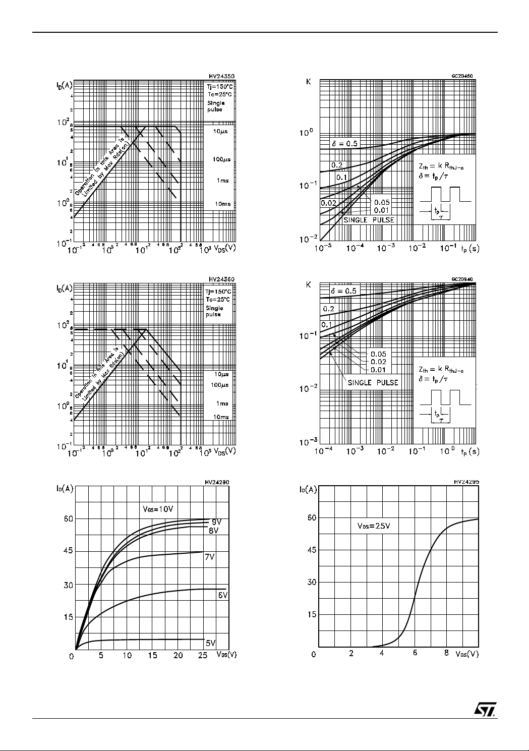
Figure 3: Safe Operating Area For TO-220/ DPAK
Figure 4: Safe Operating Area For TO-220FP
Figure 6: Thermal Impedance For TO-220/ DPAK
Figure 7: Thermal Impedance For TO-220FP
Figure 5: Output Characteristics
4/13
Figure 8: Transfer Characteristics
 Loading...