

STMicroelectronics STP16C596 Technical data
STP16C596
16-BIT CONSTANT CURRENT LED SINK DRIVER
■ 16 CONSTANT CURRENT OUTPUT
CHANNELS
■ ADJUST ABLE OUTPUT CURRENT
THROUGH EXTERNAL RESISTOR
■ SERIAL DATA IN/PARALLEL DATA OUT
■ SERIAL OUT CHANGE STATE ON THE
FALLI NG EDGE S OF CLOC K
■ OUTPUT CURRENT: 15-120 mA
■ 25 MHz CLOCK FREQ.
■ A VAILABLE IN HIGH THERM AL TSSOP
EXPOSED PAD
■ EFFICIENCY PACKAGE
DESCRIPTION
The STP16C596 is a monolithic, medium-voltage,
low current power 16-bit shift register designed for
LED panel d isplays. The STP16C596 contains a
16-bit serial-in, parallel-out shift register that feeds
a 16-bitD-type storage register. In the output
stage, sixteen regulated current sources are
designed to provide 15-120mA constant current to
drive the LEDs.
The serial output change state on the falling edges
of clock, this special feature will provide an
improved performance of the application when the
clock signal is skewed because the daisy chain is
too long.
DIP-24
TSSOP24
SO-24
TSSOP24
(exposed pad)
Through an external resistor, users may adjust the
STP16C596 output current, controlling in this way
the light intensity of LEDs.
The STP16C596 guarantees a 16V output drivi ng
capability, allowing users to connect more LEDs in
series. The high clock frequency, 25 MHz, also
satisfies the system demand for high volume data
transmission. Compared wi th a standard TSSOP
package, the TSSOP exposed pad increases heat
dissipation capability by a 2.5 factor.
Table 1: Order Codes
Part Number Package Comments
STP16C596B1R DIP-24 15 parts per tube
STP16C596M SO-24 (Tube) 40 parts per tube
STP16C596MTR SO-24 (Tape & Reel) 1000 parts per reel
STP16C596TTR TSSOP24 (Tape & Reel) 2500 parts per reel
STP16C596XTTR TSSOP24 Exposed-Pad (Tape & Reel) 2500 parts per reel
Rev. 8
1/18July 2005
STP16C596
Table 2: Current Accuracy
Output Voltage
Between bits Between ICs
≥ 0.7V TYP. ± 3% ± 10% 15 to 120 mA
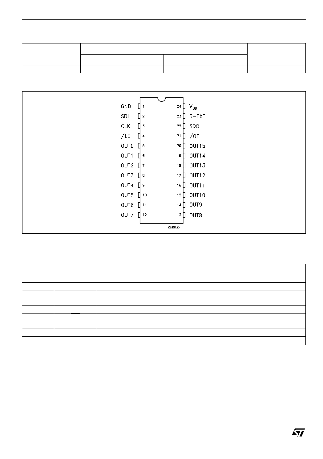
Figure 1: Pin Connection (Note 1)
Current accuracy
Output Current
Note 1: The exposed Pad is electrica l l y not connecte d.
Table 3: Pin Description
PIN N° Symbol Name and Function
1 GND Ground Terminal
2 SDI Serial data input terminal
3 CLK Clock input terminal
4 /LE Latch input terminal
5-20 OUT 0-15 Output terminal
21 /OE
22 SDO Serial data out terminal
23 R-EXT Input terminal of an external resistor for constant current programing
24 V
DD
Input terminal of output enable (active low)
Supply voltage terminal
2/18
STP16C596
Table 4: Absolute Maximum Ratings
Symbol Parameter Value Unit
V
V
I
V
I
GND
f
CLK
T
OPR
T
STG
Absolute Maximum Ratings are t hose values be yond which dam age to the devi ce may occu r. Under these conditions, fun ct i onal opera tion
is not implied.
Table 5: Thermal Data
Supply Voltage
DD
Output Voltage
O
Output Current
O
Input Voltage -0.4 to VDD+0.4
I
GND Termin al Current
Clock Frequency
Operating Temperature Range
Storage Temperature Range
0 to 7 V
-0.5 to 16 V
120 mA
V
1920 mA
25 MHz
-40 to +125 °C
-65 to +150 °C
Symbol Parameter DIP-24 SO-24 TSSOP24
R
thj-amb
(*) The exposed pad should be solde red directly to the PCB to realize the th ermal benefit s.
Thermal Resistance Junction-ambient
60 75 85 37.5 °C/W
TSSOP24 (*)
(exposed pad)
Table 6: Recommended Operating Conditions
Symbol Parameter Test Conditions Min. Typ. Max. Unit
V
V
I
I
V
V
t
wLAT
t
wCLK
t
wEN
t
SETUP(D)
t
HOLD(D)
t
SETUP(L)
f
CLK
Supply Voltage 4.5 5.0 5.5 V
DD
Output Voltage 16.0 V
O
Output Current OUTn 5 120 mA
I
O
Output Current SERIAL-OUT +1 mA
OH
Output Current SERIAL-OUT -1 mA
OL
Input Voltage 0.7V
IH
Input Voltage -0.3 0.3V
IL
DD
/LE Pulse Width VDD = 4.5 to 5.5V 20 ns
CLK Pulse Width 20 ns
/OE Pulse Width 400 ns
Setup Time for DATA 20 ns
Hold Time for DATA 15 ns
Setup Time for LATCH 15 ns
Clock Frequency Cascade Operation 25 MHz
VDD+0.3 V
DD
Unit
V
3/18
STP16C596
Table 7: Electrical Characteristics (VDD=5V, T = 25°C, unless otherwise specified.)
Symbol Parameter Test Conditions Min. Typ. Max. Unit
V
V
I
V
V
I
OL1
I
OL2
∆I
∆I
R
SIN(up)
R
SIN(down)
I
DD(OFF1)
I
DD(OFF2)
I
DD(OFF3)
I
DD(ON1)
I
DD(ON2)
Input Voltage High Level 0.7V
IH
Input Voltage Low Level GND 0.3V
IL
Output Leakage Current VOH = 16 V 10 µA
OH
Output Voltage (Serial-OUT) IOL = 1mA 0.4 V
OL
Output Voltage (Serial-OUT) IOH = -1mA VDD-0.4V V
OH
Output Current VO = 0.7V R
Output Current Error
OL1
between bit (All Output ON)
OL2
VO = 0.7V R
VO = 0.7V R
VO = 0.7V R
= 910 Ω 18.6 20.4 22.4 mA
EXT
= 360 Ω 45.7 50.2 55.2 mA
EXT
= 910 Ω ± 3 ± 4 %
EXT
= 360 Ω ± 3 ± 4 %
EXT
DD
Pull-up Resistor 150 300 600 KΩ
Pull-down Resistor 100 200 400 KΩ
Supply Current (OFF) R
Supply Current (ON) R
= OPEN OUT 0 to 15 = OFF 0.3 0.6 mA
EXT
R
= 470 Ω OUT 0 to 15 = OFF 5.5 7.7
EXT
R
= 250 Ω OUT 0 to 15 = OFF 10.1 14.1
EXT
= 470 Ω OUT 0 to 15 = ON 5.5 7.7
EXT
R
= 250 Ω OUT 0 to 15 = ON 10.1 14.1
EXT
V
DD
DD
V
V
Table 8: Switching Characteristics (V
=5V, T = 25°C, unless otherwise specified.)
DD
Symbol Parameter Test Conditions Min. Typ. Max. Unit
t
PLH1
t
PLH2
t
PLH3
t
PLH
t
PHL1
t
PHL2
t
PHL3
t
PHL
Propagation Delay Time,
CLK-OUTn
, /LE = H, /OE = L
Propagation Delay Time,
-OUTn, /OE = L
/LE
Propagation Delay Time,
-OUTn, /LE = H
/OE
Propagation Delay Time,
CLK-SDO
Propagation Delay Time,
CLK-OUTn
, /LE = H, /OE = L
Propagation Delay Time,
-OUTn, /OE = L
/LE
Propagation Delay Time,
-OUTn, /LE = H
/OE
Propagation Delay Time,
CLK-SDO
t
Output Rise Time 160 200 ns
r
t
Output Fall Time 15 25 ns
f
V
= 5 V VIH = V
DD
DD
VIL = GND CL = 13pF
I
= 40mA VL = 3 V
O
R
= 470 Ω RL = 65 Ω
EXT
200 280 ns
160 250 ns
145 200 ns
15 30 ns
15 30 ns
15 30 ns
45 60 ns
15 300 ns
4/18
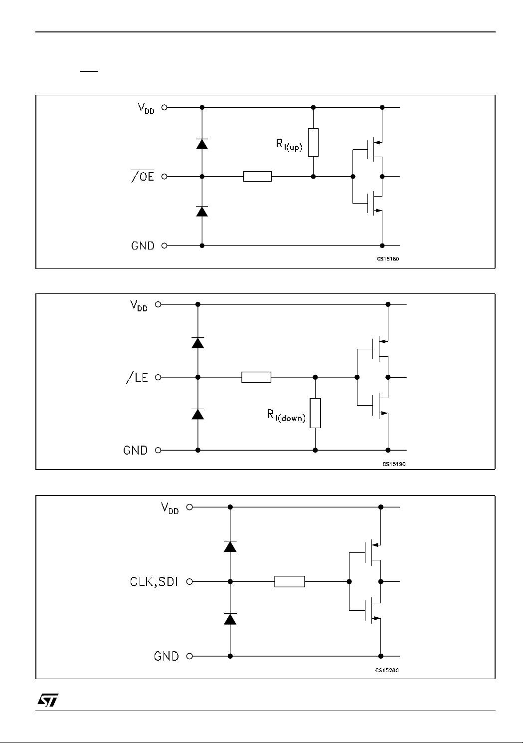
EQUIVALENT CIRCUIT OF INPUTS AND OUTPUTS
STP16C596
Figure 2: / OE
Figure 3: /LE Termin al
Terminal
Figure 4: CLK, SDI Terminal
5/18
STP16C596
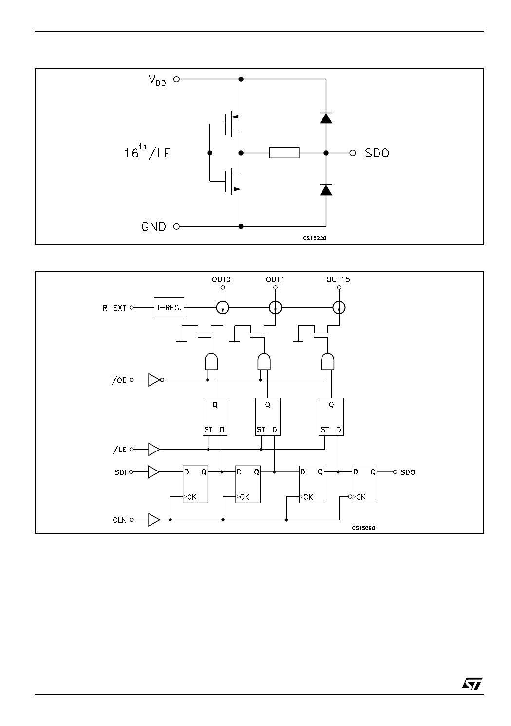
Figure 5: SDO Terminal
Figure 6: Block Diagram
6/18
 Loading...