Page 1

STI150N10F7,
$0Y
'7$%
*
6
I PAK
2
TO-220
1
2
3
TA B
1
2
3
TAB
STP150N10F7
N-channel 100 V, 0.0036 Ω typ., 110 A, STripFET™ F7
2
Power MOSFETs in I
Features
PAK and TO-220 packages
Datasheet − production data
Figure 1. Internal schematic diagram
Order codes V
STI150N10F7
STP150N10F7
DSRDS(on)maxID
100 V 0.0042 Ω 110 A 250 W
• Among the lowest R
on the market
DS(on)
P
TOT
• Excellent figure of merit (FoM)
• Low Crss/Ciss ratio for EMI immunity
• High avalanche ruggedness
Applications
• Switching applications
Description
These N-channel Power MOSFETs utilize
STripFET™ F7 technology with an enhanced
trench gate structure that results in very low onstate resistance, while also reducing internal
capacitance and gate charge for faster and more
efficien t switching.
Table 1. Device summary
Order codes Marking Package Packaging
STI150N10F7
STP150N10F7 TO-220
August 2014 DocID024552 Rev 4 1/15
This is information on a product in full production.
150N10F7
2
I
PAK
Tube
www.st.com
Page 2

Contents STI150N10F7, STP150N10F 7
Contents
1 Electrical ratings . . . . . . . . . . . . . . . . . . . . . . . . . . . . . . . . . . . . . . . . . . . . 3
2 Electrical characteristics . . . . . . . . . . . . . . . . . . . . . . . . . . . . . . . . . . . . . 4
2.1 Electrical characteristics (curves) . . . . . . . . . . . . . . . . . . . . . . . . . . . . 6
3 Test circuits . . . . . . . . . . . . . . . . . . . . . . . . . . . . . . . . . . . . . . . . . . . . . . 8
4 Package mechanical data . . . . . . . . . . . . . . . . . . . . . . . . . . . . . . . . . . . . . 9
5 Revision history . . . . . . . . . . . . . . . . . . . . . . . . . . . . . . . . . . . . . . . . . . . 14
2/15 DocID024552 Rev 4
Page 3

STI150N10F7, STP150N10F 7 Electrical ratings
1 Electrical ratings
Table 2. Absolute maximum ratings
Symbol Parameter Value Unit
V
DS
V
GS
I
D
I
D
I
DM
P
TOT
E
AS
T
T
stg
1. Pulse width is limited by safe operating area
2. Starting Tj=25 °C, ID=30 A, VDD=50 V
Drain-source voltage 100 V
Gate- source voltage ±20 V
Drain current (continuous) at TC = 25 °C 110 A
Drain current (continuous) at TC = 100 °C 110 A
(1)
Drain current (pulsed) 440 A
Total dissipation at TC = 25 °C 250 W
(2)
Single pulse avalanche energy 495 mJ
Operating junction temperature
J
-55 to 175
Storage temperature °C
Table 3. Thermal data
Symbol Parameter Value Unit
R
thj-case
R
thj-amb
Thermal resistance jun ction-case max 0.6 °C/W
Thermal resistance jun cti on- amb ie nt max 62.5 °C/W
°C
DocID024552 Rev 4 3/15
15
Page 4

Electrical characteristics STI150N10F7, STP150N10F7
2 Electrical characteristics
(TC = 25 °C unless otherwise specified)
Table 4. On /off states
Symbol Parameter Test conditions Min. Typ. Max. Unit
V
(BR)DSS
I
DSS
I
GSS
V
GS(th)
R
DS(on)
Drain-source
breakdown voltage
Zero gate voltage
drain current
Gate-body leakage
current
VGS = 0, ID = 250 µA 100 V
V
= 0, V
GS
V
= 0,
GS
V
= 100 V, TC=125 °C
DS
= 100 V 1 µA
DS
100 µA
VDS = 0, VGS = +20 V 100 nA
Gate threshold voltage VDS = VGS, ID = 250 µA 2.5 4.5 V
Stat ic d rain-s ource on-
resistance
V
= 10 V, ID = 55 A 0.0036 0.0042 Ω
GS
Table 5. Dynamic
Symbol Parameter Test conditions Min. Typ. Max. Unit
C
C
C
Input capacitance
iss
Output capacitance -
oss
Reverse transfer
rss
VDS = 50 V, f = 1 MHz,
VGS = 0
capacitance
Q
Q
Q
Total gate charge
g
Gate-source charge - 47 - nC
gs
Gate-drain charge - 26 - nC
gd
VDD = 50 V, ID = 110 A,
VGS = 10 V
(see Figure 14)
-8115-pF
1510
-
67
-pF
-pF
-117-nC
Table 6. Switching times
Symbol Parameter Test conditions Min. Typ. Max. Unit
t
d(on)
t
d(off)
4/15 DocID024552 Rev 4
Turn-on delay time
= 50 V, ID = 55 A,
V
t
Rise time - 57 - ns
r
Turn-off delay time - 72 - ns
t
Fall time - 33 - ns
f
DD
R
= 4.7 Ω, V
G
(see Figure 13)
GS
-33-ns
= 10 V
Page 5

STI150N10F7, STP150N10F 7 Electrical ch ara cter ist ics
Table 7. Source drain diode
Symbol Parameter Test conditions Min. Typ. Max. Unit
I
SD
I
SDM
V
SD
t
Q
I
RRM
1. Pulse width limited by safe operating area
2. Pulsed: pulse duration = 300 µs, duty cycle 1.5%.
Source-drain current - 110 A
(1)
Source-drain current (pulsed) - 440 A
(2)
Forward on voltage ISD = 110 A, VGS = 0 - 1.2 V
Reverse recovery time
rr
Reverse recovery charge - 165 nC
rr
Reverse recovery current - 4.7 A
ISD = 110 A, di/dt = 100 A/µs
VDD = 80 V, TJ=150 °C
(see Figure 15)
-70 ns
DocID024552 Rev 4 5/15
15
Page 6

Electrical characteristics STI150N10F7, STP150N10F7
I
D
10
1
0.1
1
V
DS
(V)
10
(A)
Operation in this area is
Limited by max R
DS(on)
10ms
1ms
100µs
0.1
Tj=175°C
Tc=25°C
Single pulse
100
AM18051v1
Single pulse
δ=0.5
0.05
0.02
0.01
0.1
0.2
K
10
t
p(s)
-4
10
-3
10
-1
10
-5
10
-2
10
-2
10
-1
10
0
c
AM18052v1
I
D
250
150
50
0
0
2
V
DS
(V)
4
(A)
6
350
400
5V
6V
VGS=10V
100
200
300
7V
8V
8
AM18042v1
V
GS
6
4
2
0
0
40
Q
g
(nC)
(V)
120
8
80
10
VDD=50V
I
D
=110A
12
AM18044v1
2.1 Electrical characteristics (curves)
Figure 2. Safe operating area Figure 3. Thermal impedance
Figure 4. Output characteristics Figure 5. Transfer characteristics
(A)
300
250
200
I
D
AM18043v1
VDS=4V
150
100
50
0
0
Figure 6. Gate charge vs gate-source voltage Figure 7. Static drain-source on-resistance
R
DS(on)
Ω)
(m
2
4
VGS=10V
6
3.62
3.61
3.60
3.59
3.58
3.57
3.56
3.55
20
40
60
0
80
6/15 DocID024552 Rev 4
8
V
GS
(V)
AM18054v1
D
(A)
I
100
Page 7

STI150N10F7, STP150N10F 7 Electrical ch ara cter ist ics
C
3000
2000
1000
0
0
40
V
DS
(V)
(pF)
20
60
Ciss
Coss
Crss
80
100
4000
6000
7000
8000
5000
AM18046v1
R
DS(on)
1.8
1.2
0.8
0.4
T
J
(°C)
(norm)
0.6
1
1.4
1.6
2
-75
25
75
-25
125
AM18048v1
ID=55A
V
GS
=10V
V
SD
0
40
I
SD
(A)
(V)
20
100
60
80
0.3
0.4
0.5
0.6
TJ=-55°C
TJ=175°C
TJ=25°C
0.7
1
0.8
0.9
AM18055v1
Figure 8. Capacitance variations Figure 9. Normalized gate threshold voltage vs
V
GS(th)
(norm)
1.1
1
0.9
0.8
0.7
0.6
0.5
0.4
-75
temperature
-25
25
I
D
=250µA
75
125
AM18047v1
J
(°C)
T
Figure 10. Normalized on-resistance vs
temperature
Figure 12. Source-drain diode forward
characteristics
Figure 11. Normalized V
V
(BR)DDS
(norm)
1.04
1.03
1.02
1.01
1
0.99
0.98
0.97
0.96
-75
-25
25
(BR)DSS
ID=1mA
75
vs temperature
AM18049v1
J
(°C)
125
T
DocID024552 Rev 4 7/15
15
Page 8

Test circuits STI150N10F7, STP150N10F7
AM01468v1
VGS
PW
VD
RG
RL
D.U.T.
2200
μF
3.3
μF
V
DD
AM01469v1
VDD
47kΩ
1kΩ
47kΩ
2.7kΩ
1kΩ
12V
V
i=20V=VGMAX
2200
μF
PW
IG=CONST
100Ω
100nF
D.U.T.
V
G
AM01470v1
A
D
D.U.T.
S
B
G
25
Ω
A
A
B
B
R
G
G
FAST
DIODE
D
S
L=100μH
μF
3.3
1000
μF
V
DD
AM01472v1
V(BR)DSS
VDD
VDD
VD
IDM
ID
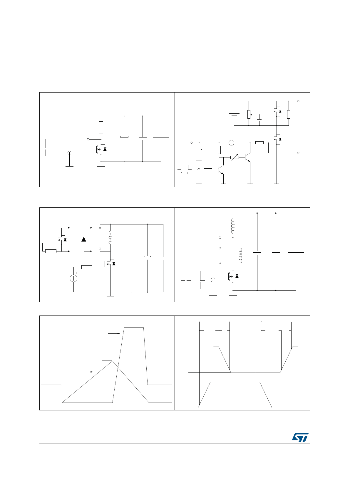
3 Test circuits
Figure 13. Switching times test circuit for
resistive load
Figure 15. Test circuit for inductive load
switching and diode recovery times
Figure 14. Gate charge test circuit
Figure 16. Unclamped inductive load test circuit
L
VD
2200
μF
3.3
μF
VDD
Figure 17. Unclamped inductive waveform Figure 18. Switching time waveform
8/15 DocID024552 Rev 4
ID
Vi
D.U.T.
Pw
AM01471v1
tdon
ton
tr
90%
tdoff
toff
tf
90%
10%
0
10%
VDS
90%
V
GS
10%
0
AM01473v1
Page 9

STI150N10F7, STP150N10F7 Package mechanical data
4 Package mechanical data
In order to meet environmental requirements, ST offers these devices in different grades of
®
ECOPACK
specifications, grade definitions and product status are available at: www.st.com.
ECOPACK
packages, depending on their level of environmental compliance. ECOPACK®
®
is an ST trademark.
DocID024552 Rev 4 9/15
15
Page 10

Package mechanical data STI150N10F7, STP150N10F7
0004982_Rev_H
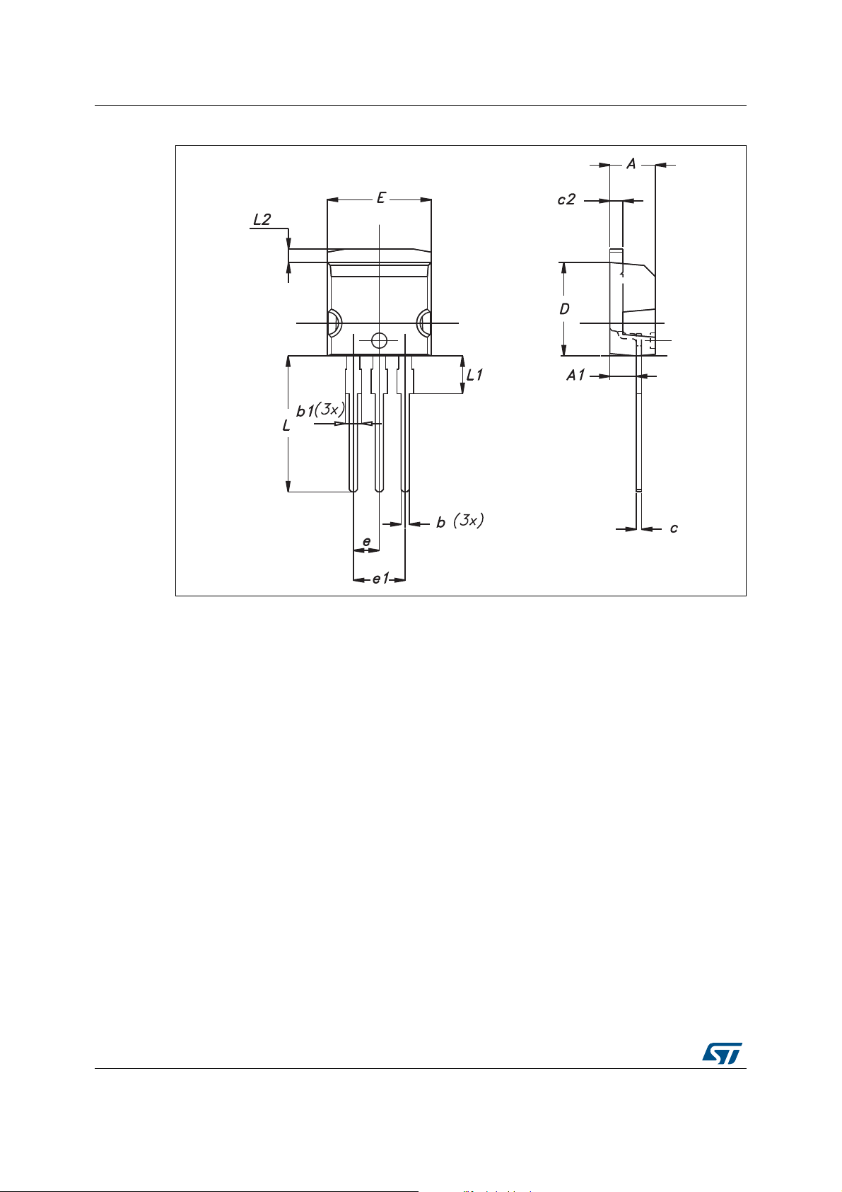
Figure 19. I²PAK (TO-262) drawing
10/15 DocID024552 Rev 4
Page 11

STI150N10F7, STP150N10F7 Package mechanical data
Table 8. I²PAK (TO-262) mechanical data
mm.
DIM.
min. typ max.
A 4.40 4.60
A1 2.40 2.72
b 0.61 0.88
b1 1.14 1.70
c 0.49 0.70
c2 1.23 1.32
D 8.95 9.35
e 2.40 2.70
e1 4.95 5.15
E10 10.40
L13 14
L1 3.50 3.93
L2 1.27 1.40
DocID024552 Rev 4 11/15
15
Page 12

Package mechanical data STI150N10F7, STP150N10F7
BW\SH$B5HYB7
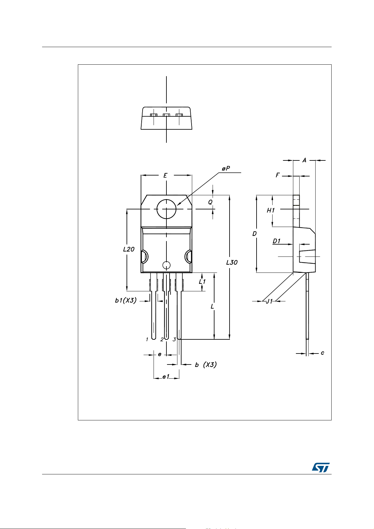
Figure 20. TO-220 type A drawing
12/15 DocID024552 Rev 4
Page 13

STI150N10F7, STP150N10F7 Package mechanical data
Table 9. TO-220 type A mechanical data
mm
Dim.
Min. Typ. Max.
A4.40 4.60
b0.61 0.88
b1 1.14 1.70
c0.48 0.70
D 15.25 15.75
D1 1.27
E 10 10.40
e2.40 2.70
e1 4.95 5.15
F1.23 1.32
H1 6.20 6.60
J1 2.40 2.72
L13 14
L1 3.50 3.93
L20 16.40
L30 28.90
∅
P3.75 3.85
Q2.65 2.95
DocID024552 Rev 4 13/15
15
Page 14

Revision history STI150N10F7, STP150N10F7
5 Revision history
Table 10. Document revision history
Date Revision Changes
16-Apr-2013 1 First release.
– The part number STH150N10F7-2 has been moved to a separate
datasheet
– Added: I
2
PAK package
– Modified: Figure1
– Modified: ID and IDM values in Table 2
22-Jan-2014 2
– Modified: R
– Modified: R
value in Table 3
thj-case
values in Table 4
DS(on)
– Modified: VSD, ID and the entire typical values in Table 5, 6 and 7
– Updated: Figure 13, 14, 15 and 16
– Updated: Section 4: Package mechanical data
– Added: Section 2.1: Electrical characteristics (curves)
– Minor text changes
– Datasheet status promoted from preliminary data to production
24-Feb-2014 3
data
– Modified: Figure10
– Minor text changes
– Updated title, features and description in cover page.
20-Aug-2014
– Added E
parameter in Table 2: Absolute maximum ratings.
AS
– Minor text changes
14/15 DocID024552 Rev 4
Page 15

STI150N10F7, STP150N10F 7
IMPORTANT NOTICE – PLEASE READ CAREFULLY
STMicroelectronics NV and it s subsidiaries (“ST”) reserve th e right to make changes, corrections, enhancements, modifications, and
improvements to ST produc ts and /or to this document at any time witho ut notice. Purchasers should obt ain the lat est relevan t info rmation on
ST products before placing orders. ST products are sold pursuant to ST’ s terms and conditions of sale in pla ce at the time of order
acknowledgement.
Purchasers are solely r espon si ble for t he cho ic e, s elect ion, a nd use of ST produc ts and ST assume s no l iabil ity f or app lication as sist ance or
the design of Purchasers’ products.
No license, express or implied , to any intellectual proper ty right is granted by ST herein.
Resale of ST products with provis ions different from the information set forth herein sha ll void any warranty granted by ST for such product.
ST and the ST logo are trademarks of ST. All other product or service names are the property of their respectiv e owners.
Information in this document supers edes and replaces information previously supplied in any prior versions of this document.
© 2014 STMicroelectronics – All rights reserved
DocID024552 Rev 4 15/15
15
 Loading...