

STMicroelectronics STM705, STM706, STM707, STM708, STM813L Technical data
FEAT URES SUMMARY
■ 5V OPERATING VOLTAGE
■ PRECISION V
– STM705/707/813L
4.50V ≤ V
– STM706/708
4.25 ≤ V
■ RST AND RST OUTPUTS
■ 200ms (TYP) t
■ WATCHDOG TIMER - 1.6sec (TYP)
■ MANUAL RESET INPUT (MR)
■ POWER-FAIL COMPARATOR (PFI/P FO )
■ LOW SUPPLY CURRENT - 40µA (TYP)
■ GUARANTEED RST (RST) ASSERTION
DOWN TO V
■ OPERATING TEMPERAT UR E:
–40°C to 85°C (Industrial Grade)
CC
RST
RST
rec
CC
≤ 4.50V
= 1.0V
MONITO R
≤ 4.75V
STM705, STM706,
STM707, STM708, STM813L
5V Supervisor
Figure 1. Packages
8
1
SO8 (M)
TSSOP8 3x3 (DS)
Table 1. Device Options
Watchdog
Input
STM705 ✔✔✔ ✔✔
STM706 ✔✔✔ ✔✔
STM707 ✔✔✔✔
STM708 ✔✔✔✔
STM813L ✔✔ ✔✔✔
Note: 1. Push-pull Output
Watchdog
Output
Active-Low
(1)
RST
Active-High
(1)
RST
Manual
Reset Input
Power-fail
Comparator
1/27March 2005

STM705/706/707/708/813L
TABLE OF CONTENTS
FEATURES SUMMARY . . . . . . . . . . . . . . . . . . . . . . . . . . . . . . . . . . . . . . . . . . . . . . . . . . . . . . . . . . . . . 1
Figure 1. Packages. . . . . . . . . . . . . . . . . . . . . . . . . . . . . . . . . . . . . . . . . . . . . . . . . . . . . . . . . . . . . . 1
Table 1. Device Options . . . . . . . . . . . . . . . . . . . . . . . . . . . . . . . . . . . . . . . . . . . . . . . . . . . . . . . . . 1
SUMMARY DESCRIPTION. . . . . . . . . . . . . . . . . . . . . . . . . . . . . . . . . . . . . . . . . . . . . . . . . . . . . . . . . . . 4
Figure 2. Logic Diagram (STM705/706/813L ). . . . . . . . . . . . . . . . . . . . . . . . . . . . . . . . . . . . . . . . . . 4
Figure 3. Logic Diagram (STM707/708) . . . . . . . . . . . . . . . . . . . . . . . . . . . . . . . . . . . . . . . . . . . . . . 4
Table 2. Signal Names . . . . . . . . . . . . . . . . . . . . . . . . . . . . . . . . . . . . . . . . . . . . . . . . . . . . . . . . . . 4
Figure 4. STM705/706/813L SO8 Connec tions . . . . . . . . . . . . . . . . . . . . . . . . . . . . . . . . . . . . . . . . 5
Figure 5. STM705/706/813L TSSO P8 Connec tions. . . . . . . . . . . . . . . . . . . . . . . . . . . . . . . . . . . . . 5
Figure 6. STM707/708 SO8 Conne ctions. . . . . . . . . . . . . . . . . . . . . . . . . . . . . . . . . . . . . . . . . . . . . 5
Figure 7. STM707/708 TSSOP8 Connections . . . . . . . . . . . . . . . . . . . . . . . . . . . . . . . . . . . . . . . . . 5
Pin Descriptions . . . . . . . . . . . . . . . . . . . . . . . . . . . . . . . . . . . . . . . . . . . . . . . . . . . . . . . . . . . . . . . 6
Table 3. Pin Description. . . . . . . . . . . . . . . . . . . . . . . . . . . . . . . . . . . . . . . . . . . . . . . . . . . . . . . . . . 6
Figure 8. Block Diagram (STM705/706/813L) . . . . . . . . . . . . . . . . . . . . . . . . . . . . . . . . . . . . . . . . . 7
Figure 9. Block Diagram (STM707/708). . . . . . . . . . . . . . . . . . . . . . . . . . . . . . . . . . . . . . . . . . . . . . 7
Figure 10.Hardware Hookup . . . . . . . . . . . . . . . . . . . . . . . . . . . . . . . . . . . . . . . . . . . . . . . . . . . . . . . 8
OPERATION . . . . . . . . . . . . . . . . . . . . . . . . . . . . . . . . . . . . . . . . . . . . . . . . . . . . . . . . . . . . . . . . . . . . . . 9
Reset Output . . . . . . . . . . . . . . . . . . . . . . . . . . . . . . . . . . . . . . . . . . . . . . . . . . . . . . . . . . . . . . . . . . 9
Push-button Reset Input. . . . . . . . . . . . . . . . . . . . . . . . . . . . . . . . . . . . . . . . . . . . . . . . . . . . . . . . . 9
Watchdog Input (STM705/706/813L) . . . . . . . . . . . . . . . . . . . . . . . . . . . . . . . . . . . . . . . . . . . . . . . 9
Watchdog Output (STM705/706/813L). . . . . . . . . . . . . . . . . . . . . . . . . . . . . . . . . . . . . . . . . . . . . . 9
Power-fail Input/Output. . . . . . . . . . . . . . . . . . . . . . . . . . . . . . . . . . . . . . . . . . . . . . . . . . . . . . . . . . 9
Ensuring a Valid Reset Output Down to V
= 0V . . . . . . . . . . . . . . . . . . . . . . . . . . . . . . . . . . . 10
CC
Figure 11.Reset Output Valid to Ground Circuit . . . . . . . . . . . . . . . . . . . . . . . . . . . . . . . . . . . . . . . 10
Interfacing to Microprocessors with Bi-directional Reset Pins . . . . . . . . . . . . . . . . . . . . . . . . 10
Figure 12.Interfacing to Microprocessors with Bi-directional Reset I/O. . . . . . . . . . . . . . . . . . . . . . 10
TYPICAL OPERATING CHARACTERISTICS . . . . . . . . . . . . . . . . . . . . . . . . . . . . . . . . . . . . . . . . . . . 11
Figure 13.Supply Current vs. Temperature (no load) . . . . . . . . . . . . . . . . . . . . . . . . . . . . . . . . . . . 11
Figure 14.V
Threshold vs. Temperature . . . . . . . . . . . . . . . . . . . . . . . . . . . . . . . . . . . . . . . . . . .11
PFI
Figure 15.Reset Comparator Propagation Delay vs. Temperature . . . . . . . . . . . . . . . . . . . . . . . . . 12
Figure 16.Power-up t
vs. Temperature . . . . . . . . . . . . . . . . . . . . . . . . . . . . . . . . . . . . . . . . . . . . 12
rec
Figure 17.Normalized Reset Threshold vs. Temperature . . . . . . . . . . . . . . . . . . . . . . . . . . . . . . . . 13
Figure 18.Watchdog Time-out Period vs. Temperature . . . . . . . . . . . . . . . . . . . . . . . . . . . . . . . . . 13
Figure 19.PFI to PFO
Figure 20.Output Voltage vs. Load Current (V
Figure 21.Output Voltage vs. Load Current (V
Figure 22.RST
Output Voltage vs. Supply Voltage . . . . . . . . . . . . . . . . . . . . . . . . . . . . . . . . . . . . . 15
Propagation Delay vs. Temperature . . . . . . . . . . . . . . . . . . . . . . . . . . . . . . . 14
= 5V; V
CC
= 0V; V
CC
= 2.8V; TA = 25°C). . . . . . . . . . . . . . 14
BAT
= 2.8V; TA = 25°C). . . . . . . . . . . . . . 15
BAT
Figure 23.RST Output Voltage vs. Supply Voltage . . . . . . . . . . . . . . . . . . . . . . . . . . . . . . . . . . . . .16
Figure 24.RST
Response Time (Assertion). . . . . . . . . . . . . . . . . . . . . . . . . . . . . . . . . . . . . . . . . . . 16
Figure 25.RST Response Time (Assertion) . . . . . . . . . . . . . . . . . . . . . . . . . . . . . . . . . . . . . . . . . . .17
2/27

STM705/706/707/708/813L
Figure 26.Power-fail Comparator Response Time (Assertion) . . . . . . . . . . . . . . . . . . . . . . . . . . . . 17
Figure 27.Power-fail Comparator Response Time (De-Assertion) . . . . . . . . . . . . . . . . . . . . . . . . . 18
Figure 28.Maximum Transient Duration vs. Reset Threshold Overdrive. . . . . . . . . . . . . . . . . . . . . 18
MAXIMUM RATING. . . . . . . . . . . . . . . . . . . . . . . . . . . . . . . . . . . . . . . . . . . . . . . . . . . . . . . . . . . . . . . . 19
Table 4. Absolute Maximum Ratings. . . . . . . . . . . . . . . . . . . . . . . . . . . . . . . . . . . . . . . . . . . . . . . 19
DC AND AC PARAMETERS. . . . . . . . . . . . . . . . . . . . . . . . . . . . . . . . . . . . . . . . . . . . . . . . . . . . . . . . . 20
Table 5. Operating and AC Measurement Conditions. . . . . . . . . . . . . . . . . . . . . . . . . . . . . . . . . . 20
Figure 29.AC Testing Input/Output Waveforms. . . . . . . . . . . . . . . . . . . . . . . . . . . . . . . . . . . . . . . . 20
Figure 30.Power-fail Comparator Waveform. . . . . . . . . . . . . . . . . . . . . . . . . . . . . . . . . . . . . . . . . . 20
Figure 31.MR
Figure 32.Watchdog Timing (STM705/706/8 13L) . . . . . . . . . . . . . . . . . . . . . . . . . . . . . . . . . . . . . . 21
Table 6. DC and A C Characteristics . . . . . . . . . . . . . . . . . . . . . . . . . . . . . . . . . . . . . . . . . . . . . . . 21
PACKAGE MECHANICAL . . . . . . . . . . . . . . . . . . . . . . . . . . . . . . . . . . . . . . . . . . . . . . . . . . . . . . . . . . 23
Figure 33.SO8 – 8-lead Plastic Small Outline, 150 mils body width, Package Mechanical. . . . . . . 23
Table 7. S O8 – 8-lead Plast ic Small Outline, 150 mils body widt h, Package Mechanical Data . . 23
Figure 34.TSSOP8 – 8-lead, Thin Shrink Small Outline, 3x3mm body size, Outline . . . . . . . . . . . 24
Table 8. TS SOP 8 – 8-lead, Thin Shrink Smal l Outline, 3x3mm body size , Mechanical Data . . . .24
Timing Waveform . . . . . . . . . . . . . . . . . . . . . . . . . . . . . . . . . . . . . . . . . . . . . . . . . . . 21
PART NUMBERING . . . . . . . . . . . . . . . . . . . . . . . . . . . . . . . . . . . . . . . . . . . . . . . . . . . . . . . . . . . . . . . 25
Table 9. Ordering Information Scheme . . . . . . . . . . . . . . . . . . . . . . . . . . . . . . . . . . . . . . . . . . . . . 25
Table 10.Marking Description. . . . . . . . . . . . . . . . . . . . . . . . . . . . . . . . . . . . . . . . . . . . . . . . . . . . . 25
REVISION HISTORY . . . . . . . . . . . . . . . . . . . . . . . . . . . . . . . . . . . . . . . . . . . . . . . . . . . . . . . . . . . . . . . 26
Table 11.Document Revision History. . . . . . . . . . . . . . . . . . . . . . . . . . . . . . . . . . . . . . . . . . . . . . . 26
3/27
STM705/706/707/708/813L
SUMMARY DESCRIPTION
The STM705/706/707/708/813L Supervisors are
self-contained devices which provide microprocessor supervisory functions. A precision voltage
reference and comparator m oni tors th e V
for an out-of-tolerance condition. When an invalid
condition occurs, the reset output (RST) is
V
CC
forced low (or high in the case of RST).
CC
input
These devices also offer a watchdog timer (except
for STM707/708) as well as a power-fail comparator to provide the system with an early warning of
impending power failure.
These devices are available in a standard 8-pin
SOIC package or a space-saving 8-pin TSSOP
package.
Figure 2. Logic Diagram (STM705/706/813L)
V
CC
WDO
WDI
MR
STM705/706;
STM813L
PFI
V
Note: 1. For STM70 5/706 only.
2. For STM813L only.
SS
RST
RST
PFO
AI08825
(1)
(2)
Figure 3. Logic Diagram (STM707/708)
V
CC
RST
MR
STM707/708
RST
PFI
PFO
V
SS
AI08826
Table 2. Signal Names
MR Push-button Reset Input
WDI Watchdog Input
4/27
WDO
RST
(1)
RST
V
CC
PFI Power-fail Input
PFO
V
SS
NC No Conn ect
Note: 1. For STM81 3L only.
Watchdog Output
Active-Low Reset Output
Active-High Reset Output
Supply Voltage
Power-fail Output
Ground
STM705/706/707/708/813L
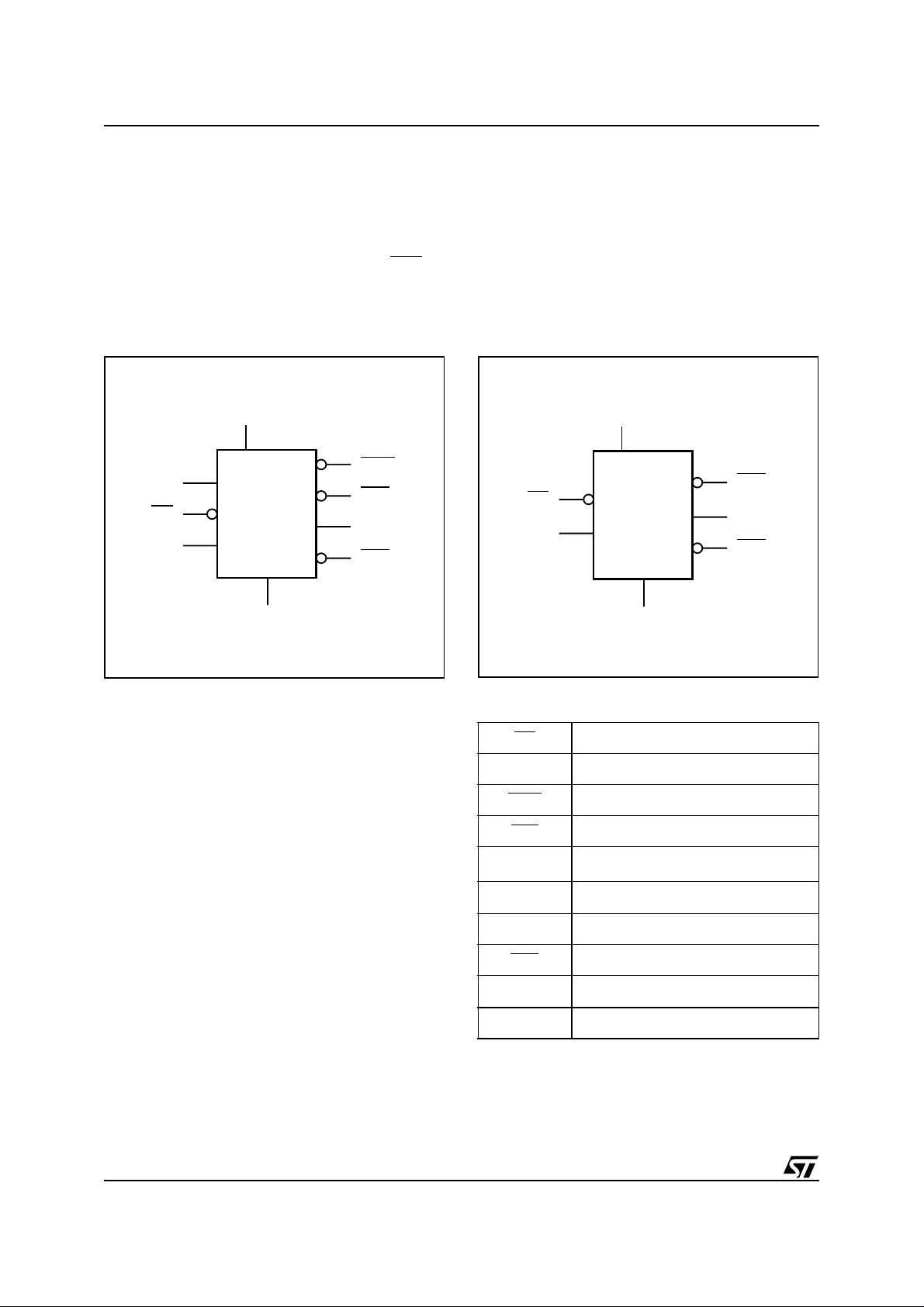
Figure 4. STM705/706/813L SO8 Connections
SO8
MR
V
V
PFI
Note: 1. For STM813L, reset outp ut is active-hi gh.
CC
SS
1
2
3
4
8
7
6
5
WDO
RST(RST)
WDI
PFO
AI08827a
(1)
Figure 5. STM705/706/813L TSSOP8 Connections
TSSOP8
(1)
CC
1
2
3
4
(RST)RST
WDO
MR
V
Note: 1. For STM813L, reset outp ut is active-hi gh.
WDI
8
PFO
7
PFI
6
V
5
SS
AI09114
Figure 6. STM707/708 SO8 Connections
SO8
MR
V
V
PFI
CC
SS
1
2
3
4
8
7
6
5
RST
RST
NC
PFO
AI08828a
Figure 7. STM707/708 TSSOP8 Connection s
TSSOP8
RST
RST
MR
V
CC
1
2
3
4
NC
8
PFO
7
PFI
6
V
5
SS
AI09115
5/27

STM705/706/707/708/813L
Pin Descrip tio ns
.A logic low on MR asserts the reset out put.
MR
Reset remains asserted as long as MR
after MR returns high. This active-low input
for t
rec
has an internal pull-up. It can be driven from a TTL
or CMOS logic line, or shorted to ground with a
switch. Leave open if unused.
WDI. If WDI remains high or low for 1.6sec, the internal watchdog timer runs out and reset (or WDO
is triggered. The internal watchdog timer clears
while reset is asserted or when WDI s ees a rising
or falling edge.
The watchdog function can be di sabled by allowing the WDI pin to float.
.It goes low when a transition does not oc-
WDO
cur on WDI within 1.6sec, and rem ain s low until a
transition occurs on WDI (indicating the watchdog
interrupt has been serviced). WDO
when V
falls below the reset threshold; howev-
CC
er, unlike the reset output, WDO
soon as V
exceeds the reset threshold.
CC
Note: For those devices with a WDO
watchdog timeout will not trigger reset unless
is connected to MR.
WDO
is low and
also goes low
goes high as
output, a
.Pulses low when triggered, and stays low
RST
whenever V
when MR
either V
CC
is below the reset threshold or
CC
is a logic low. It remains low for t
rises above the res et thresho ld, or M R
goes from low to high.
RST. Goes high with triggered, and stays high
is above the reset threshold or
CC
is a logic high. It stays high for t
falls below the reset threshold, or MR
)
whenever V
when MR
either V
CC
goes from high to low.
PFI. When PF I is less than V
otherwise, PFO
remains high. Con nect t o ground
, PFO goes low;
PFI
if unused.
.When PFI is less than V
PFO
otherwise, PFO
remains high. Leave open if un-
, PFO goes low;
PFI
used.
rec
rec
after
after
Table 3. Pin Description
Pin Name Function
STM813L
111MR
6 – 6 WDI Watchdog Input
8–8WDO
–77RST
7 8 – RST Active-High Reset Output
222
4 4 4 PFI PFI Power-fail Input
555PFO
333
– 6 – NC No Connect
STM707
STM708
STM705
STM706
Push-button Reset Input
Watchdog Output
Active-Low Reset Output
V
Supply Voltage
CC
PFO Power-fail Output
V
Ground
SS
6/27
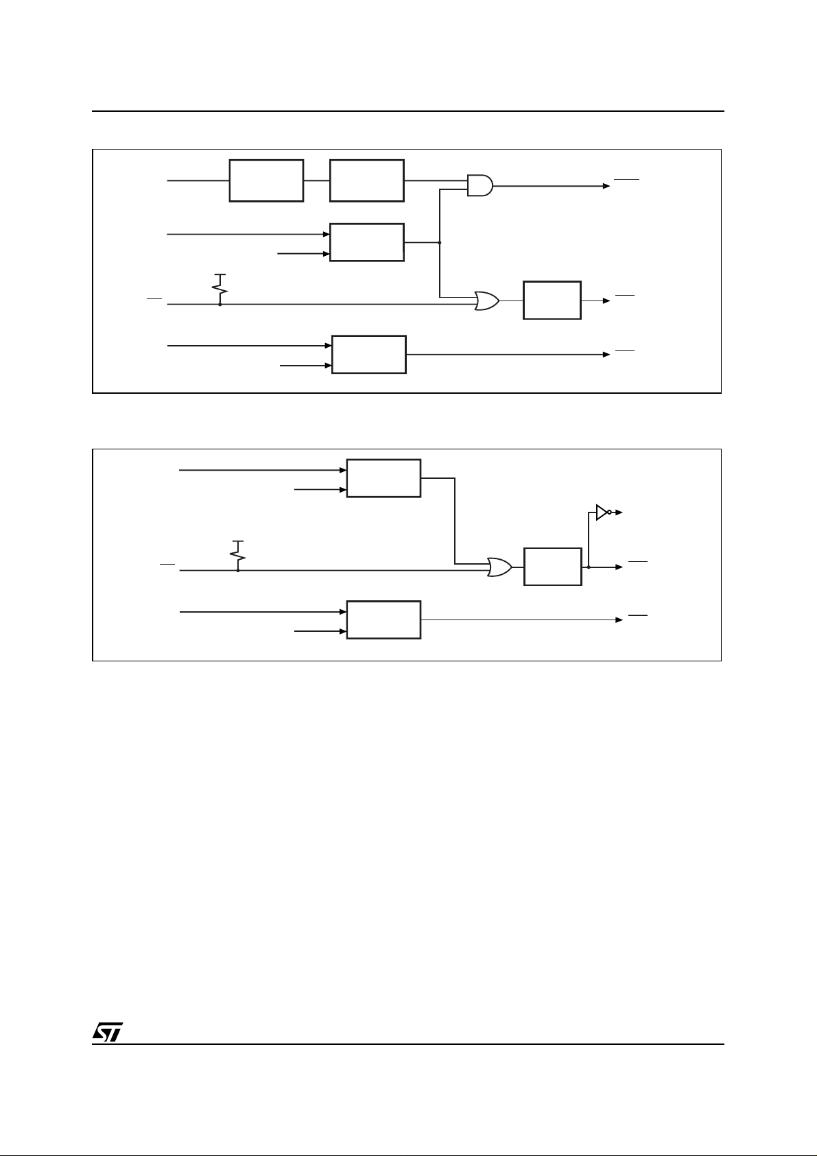
Figure 8. Block Diagram (STM705/706/813L)
STM705/706/707/708/813L
WDI
WDI
Transitional
Detector
V
CC
V
CC
V
RST
MR
PFI
V
PFI
Note: 1. For STM81 3L only.
Figure 9. Block Diagram (STM707/708)
V
CC
MR
V
CC
V
RST
WATCHDOG
TIMER
COMPARE
COMPARE
COMPARE
t
rec
Generator
t
rec
Generator
WDO
RST(RST)
PFO
AI08829
RST
RST
(1)
PFI
V
PFI
COMPARE
PFO
AI08830
7/27
STM705/706/707/708/813L
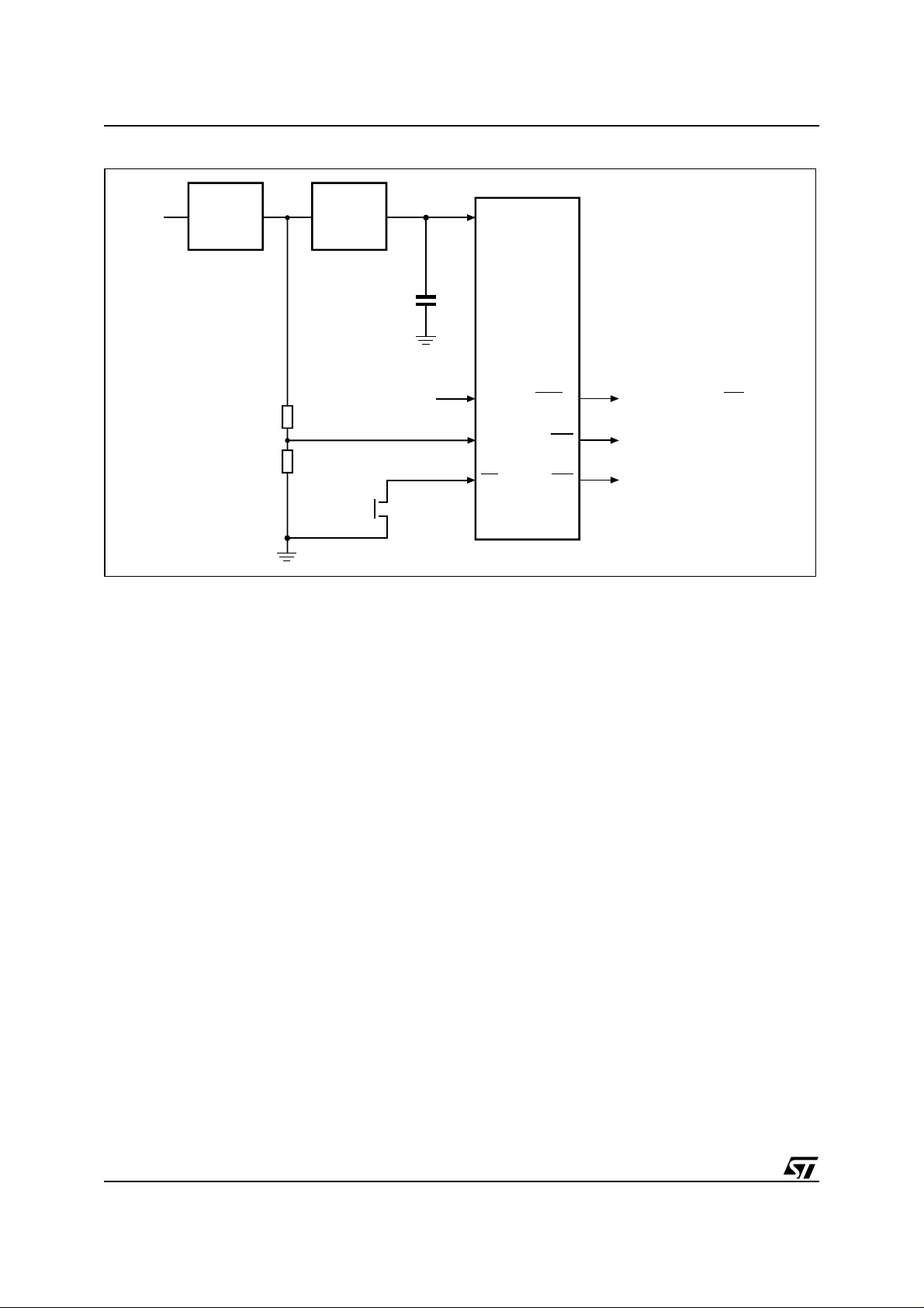
Figure 10. Hardware Hookup
Unregulated
Voltage
Note: 1. For STM70 5/ 7 06/813L.
R1
R2
Regulator
V
V
CC
IN
0.1µF
From Microprocessor
Push-button
V
CC
STM705/706/
707/708;
STM813L
(1)
WDI
PFI
MR
WDO
PFO
RST
(1)
To Microprocessor IRQ
To Microprocessor NMI
To Microprocessor Reset
AI08831
8/27

OPERATION
Reset Output
The STM705/706/707/708/813L Supervisor asserts a reset signal to the MCU whenever V
goes below the reset threshold (V
dog time-out occurs (if WDO
is tied to MR), or
when the Push-button Reset Input (MR
low. RST
is guaranteed to be a logic low (logic
high for STM707/708/813L) for V
=1V for TA = 0°C to 85°C.
to V
CC
During power-up, once V
exceeds the reset
CC
threshold an internal timer keeps RST
reset time-out period, t
. After this interval RST
rec
CC
RST
< V
), a watch-
) is ta ken
RST
low for the
returns high.
drops below the reset threshold, RST goes
If V
CC
low. Each time RST
least the reset time-out period (t
is asserted, it stays low for at
). Any time V
rec
goes below the reset threshold the internal timer
clears. The reset timer starts when V
CC
above the reset threshold.
Push-button Reset Input
A logic low on MR
asserted while MR
asserts reset. Reset remains
is low, and for t
(see Figure
rec
31., page 21) after it returns high. The MR
has an internal 40kΩ pull-up resistor, allowing it to
be left open if not used. This input can be driven
with TTL/CMOS-logic levels or with open-drain/
collector outputs. Connect a normally open momentary switch from MR
to GND to create a manual reset function; external debounce circuitry is
not required. If MR
is driven from long cables or
the device is used in a noisy environment, connect
a 0.1µF capacitor from M R
ditional noise immunity. MR
when not used.
V
CC
to GND to provide ad-
may float, or be tied to
CC
down
CC
returns
input
STM705/706/707/708/813L
Watchdog Input (STM705/706/813L)
The watchdog timer can be used to detect an outof-control MCU. If the MCU does not toggle the
Watchdog Input (WDI) within t
set is asserted. The internal 1.6sec timer is
cleared by either:
1. a reset pulse, or
2. by toggling WDI (high-to-low or low-to-high),
which can detect pulses as short as 50ns. If
WDI is tied high or low, a reset pulse is
triggered every 1.8sec (t
connected to MR
.
See F igure 32., page 21 for STM705/706/813L.
The timer remains cleared and does not count for
as long as reset is asserted. As soon as reset is released, the timer starts counting.
Note: The watchdog function may be disabled by
floating WDI or tri-stating the driver connected to
WDI. When tri-stated or disconnected, the maximum allowable leakage current is 10uA and the
maximum allowable load capacitance is 200pF.
Watchdog Output (STM705/706/813L)
When V
drops below the reset threshold, WDO
CC
will go low even if the wa tchdog timer has not yet
timed out. However, unlike the reset output, WDO
goes high as soon as VCC exceeds the reset
thres h old. W D O
may be used to generate a reset
pulse by connecting it to the MR
Power-fail Input/Output
The Power-fail Input (PFI) is compared to an internal reference voltage (independent from the V
comparator). If PFI is less than the power-fail
threshold (V
), the Power-Fail Output (PFO) will
PFI
go low. This function is intended for use as an undervoltage detector to signal a failing power supply. Typically PFI is connected through an external
voltage divider (see Figure 10. , page 8) to either
the unregulated DC input (if it is a vailable) or the
regulated output of the V
CC
divider can be set up such that the voltage at PFI
falls below V
regulated V
several milliseconds before the
PFI
input to the STM705/ 706/707/708/
CC
813L or the microprocessor drops below the minimum operating voltage.
If the comparator is unused, PFI should be connected to V
and PFO left unconnected. PFO
SS
may be connected to MR on the STM703/704/818
so that a low voltage on P FI will generat e a reset
output.
(1.6sec), the re-
WD
+ t
WD
), if WDO is
rec
input.
RST
regulator. The voltage
9/27
 Loading...