

STM690A, STM692A, STM703
STM704, STM802, STM805, STM817/8/9
5V Supervisor with Battery Switchover
FEAT URES SUMMARY
■ 5V OPERATING VOLTAGE
■ NVRAM SUPERVISO R FOR EXTERNAL
LPSRAM
■ CHIP-ENABLE GATING (STM818 only) FOR
EXTERNAL LPSRAM (7ns max PROP
DELAY)
■ RST AND RST OUTPUTS
■ 200ms (TYP) t
■ WATCHDOG TIMER - 1.6sec (TYP)
■ AUTOMATIC BATTERY SWITCHOVER
■ LOW BATTERY SUPPLY CURRENT - 0.4µA
(TYP)
■ POWER-FAIL COMPARATOR (PFI/P FO )
■ LOW SUPPLY CURRENT - 40µA (TYP)
■ GUARANTEED RST (RST) ASSERTION
DOWN TO V
■ OPERATING TEMPERAT UR E:
–40°C to 85°C (Industrial Grade)
rec
= 1.0V
CC
Figure 1. Packages
8
1
SO8 (M)
TSSOP8 3x3 (DS)*
Table 1. Device Options
(1)
Active-
High
(1)
RST
Manual
Reset
Input
Battery
Switch-
over
Power-fail
Comparator
ChipEnable
Gating
Battery
Freshness
Seal
Watchdog
Input
STM690A ✔✔ ✔ ✔
STM692A ✔✔ ✔ ✔
STM703 ✔✔✔✔
STM704 ✔✔✔✔
STM802L/M ✔✔ ✔ ✔
STM805L ✔✔✔✔
STM817L/M ✔✔ ✔ ✔ ✔
STM818L/M ✔✔ ✔ ✔✔
STM819L/M ✔✔✔✔ ✔
Note: 1. All RST and RST outp uts are push-pull.
Active-
Low
RST
* Contact local ST sales office for availability.
1/37March 2005

STM690A/692A/703/704/802/805/817/818/819
TABLE OF CONTENTS
FEATURES SUMMARY . . . . . . . . . . . . . . . . . . . . . . . . . . . . . . . . . . . . . . . . . . . . . . . . . . . . . . . . . . . . . 1
Figure 1. Packages. . . . . . . . . . . . . . . . . . . . . . . . . . . . . . . . . . . . . . . . . . . . . . . . . . . . . . . . . . . . . . 1
Table 1. Device Options . . . . . . . . . . . . . . . . . . . . . . . . . . . . . . . . . . . . . . . . . . . . . . . . . . . . . . . . . 1
SUMMARY DESCRIPTION. . . . . . . . . . . . . . . . . . . . . . . . . . . . . . . . . . . . . . . . . . . . . . . . . . . . . . . . . . . 4
Figure 2. Logic Diagram (STM690A/692A/802/805/ 817) . . . . . . . . . . . . . . . . . . . . . . . . . . . . . . . . . 4
Figure 3. Logic Diagram (STM703/704/819). . . . . . . . . . . . . . . . . . . . . . . . . . . . . . . . . . . . . . . . . . . 4
Figure 4. Logic Diagram (STM818). . . . . . . . . . . . . . . . . . . . . . . . . . . . . . . . . . . . . . . . . . . . . . . . . . 4
Table 2. Signal Names . . . . . . . . . . . . . . . . . . . . . . . . . . . . . . . . . . . . . . . . . . . . . . . . . . . . . . . . . . 4
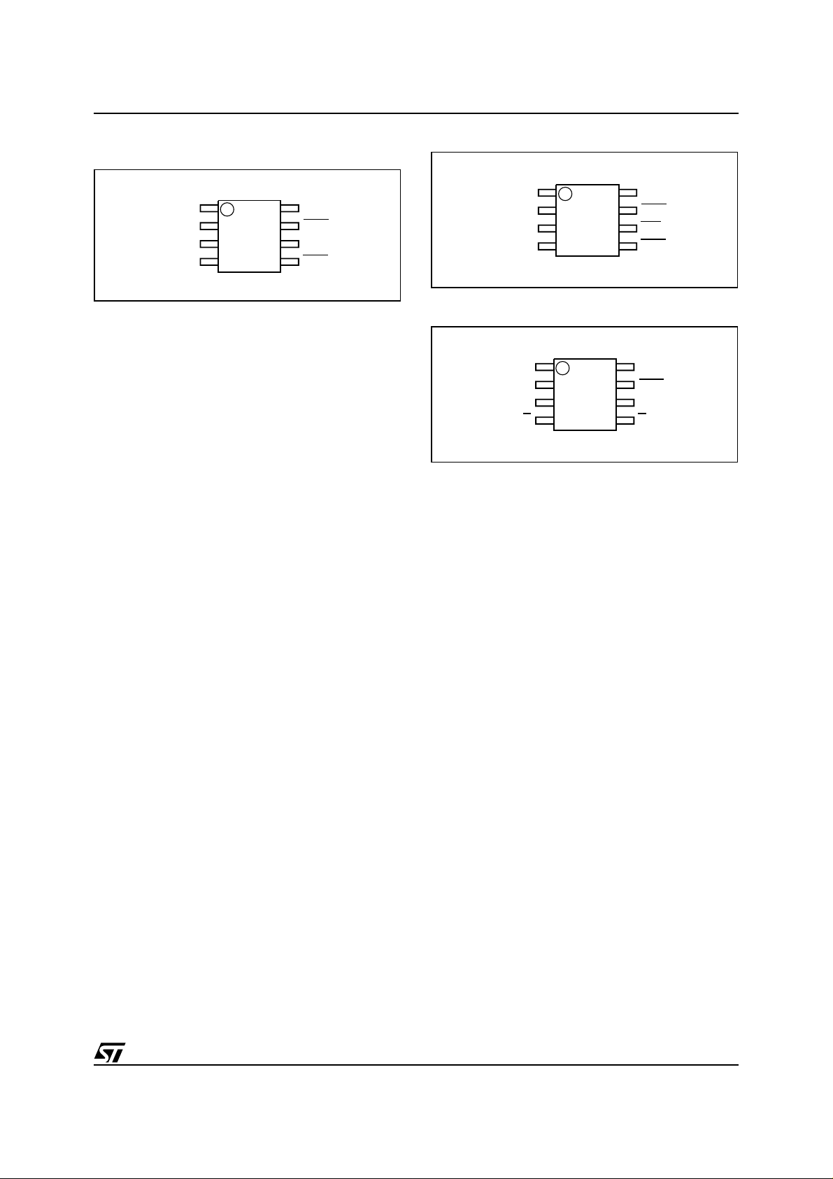
Figure 5. STM690A/692A/802/ 805/817 Connec tions . . . . . . . . . . . . . . . . . . . . . . . . . . . . . . . . . . . . 5
Figure 6. STM703/704/819 Connec tions . . . . . . . . . . . . . . . . . . . . . . . . . . . . . . . . . . . . . . . . . . . . . 5
Figure 7. STM818 Connections . . . . . . . . . . . . . . . . . . . . . . . . . . . . . . . . . . . . . . . . . . . . . . . . . . . . 5
Pin Descriptions . . . . . . . . . . . . . . . . . . . . . . . . . . . . . . . . . . . . . . . . . . . . . . . . . . . . . . . . . . . . . . . 6
Table 3. Pin Description. . . . . . . . . . . . . . . . . . . . . . . . . . . . . . . . . . . . . . . . . . . . . . . . . . . . . . . . . . 6
Figure 8. Block Diagram (STM690A/692A/802/805/ 817) . . . . . . . . . . . . . . . . . . . . . . . . . . . . . . . . . 7
Figure 9. Block Diagram (STM703/704/819) . . . . . . . . . . . . . . . . . . . . . . . . . . . . . . . . . . . . . . . . . . 7
Figure 10.Block Diagram (STM818) . . . . . . . . . . . . . . . . . . . . . . . . . . . . . . . . . . . . . . . . . . . . . . . . . 8
Figure 11.Hardware Hookup . . . . . . . . . . . . . . . . . . . . . . . . . . . . . . . . . . . . . . . . . . . . . . . . . . . . . . . 8
OPERATION . . . . . . . . . . . . . . . . . . . . . . . . . . . . . . . . . . . . . . . . . . . . . . . . . . . . . . . . . . . . . . . . . . . . . . 9
Reset Output . . . . . . . . . . . . . . . . . . . . . . . . . . . . . . . . . . . . . . . . . . . . . . . . . . . . . . . . . . . . . . . . . . 9
Push-button Reset Input (STM703/704/819) . . . . . . . . . . . . . . . . . . . . . . . . . . . . . . . . . . . . . . . . . 9
Watchdog Input (NOT available on STM703/704/ 819 ) . . . . . . . . . . . . . . . . . . . . . . . . . . . . . . . . . 9
Back-up Battery Switchover. . . . . . . . . . . . . . . . . . . . . . . . . . . . . . . . . . . . . . . . . . . . . . . . . . . . . 10
Table 4. I/O Status in Battery Back-up . . . . . . . . . . . . . . . . . . . . . . . . . . . . . . . . . . . . . . . . . . . . .10
Chip-Enable Gating (STM818 only) . . . . . . . . . . . . . . . . . . . . . . . . . . . . . . . . . . . . . . . . . . . . . . . 10
Chip Enable Input (STM818 only) . . . . . . . . . . . . . . . . . . . . . . . . . . . . . . . . . . . . . . . . . . . . . . . . .10
Chip Enable Output (STM818 only) . . . . . . . . . . . . . . . . . . . . . . . . . . . . . . . . . . . . . . . . . . . . . . . 10
Figure 12.Chip-Enable Gating. . . . . . . . . . . . . . . . . . . . . . . . . . . . . . . . . . . . . . . . . . . . . . . . . . . . . 1 1
Figure 13.Chip Enable Waveform . . . . . . . . . . . . . . . . . . . . . . . . . . . . . . . . . . . . . . . . . . . . . . . . . .11
Power-fail Input/Output (NOT available on STM818) . . . . . . . . . . . . . . . . . . . . . . . . . . . . . . . . . 12
Applications Information . . . . . . . . . . . . . . . . . . . . . . . . . . . . . . . . . . . . . . . . . . . . . . . . . . . . . . . 12
Figu r e 1 4 .Power - fail Co mpara tor Wa veform (STM 8 1 7/81 8 /8 19) . . . . . . . . . . . . . . . . . . . . . . . . . . 1 2
Figure 15.Power-fail Comparator Waveform (STM690A/692A/703/704/ 802/805) . . . . . . . . . . . . . 13
Using a SuperCap™ as a Backup Power Source. . . . . . . . . . . . . . . . . . . . . . . . . . . . . . . . . . . . 14
Negativ e- Go in g V
Transients . . . . . . . . . . . . . . . . . . . . . . . . . . . . . . . . . . . . . . . . . . . . . . . . . . 14
CC
Battery Freshness Seal (STM817/8 18/819) . . . . . . . . . . . . . . . . . . . . . . . . . . . . . . . . . . . . . . . . . 14
Figure 16.Using a SuperCap™ . . . . . . . . . . . . . . . . . . . . . . . . . . . . . . . . . . . . . . . . . . . . . . . . . . . . 1 4
Figure 17.Freshness Seal Enable Waveform . . . . . . . . . . . . . . . . . . . . . . . . . . . . . . . . . . . . . . . . . 14
TYPICAL OPERATING CHARACTERISTICS . . . . . . . . . . . . . . . . . . . . . . . . . . . . . . . . . . . . . . . . . . . 15
Figure 18.V
Figure 19.V
2/37
CC
BAT
-to-V
-to-V
On-Resistance vs. Temperature . . . . . . . . . . . . . . . . . . . . . . . . . . . . . . . . 15
OUT
On-Resistance vs. Temperature. . . . . . . . . . . . . . . . . . . . . . . . . . . . . . . . 15
OUT

STM690A/692A/703/704/802/805/817/818/819
Figure 20.Supply Current vs. Temperature (no load) . . . . . . . . . . . . . . . . . . . . . . . . . . . . . . . . . . . 16
Figure 21.Battery Current vs. Temperature. . . . . . . . . . . . . . . . . . . . . . . . . . . . . . . . . . . . . . . . . . . 16
Figure 22.V
Figure 23.Reset Comparator Propagation Delay vs. Temperature (Other than STM817/818/819) 17
Figure 24.Reset Comparator Propagation Delay vs. Temperature (V
Figure 25.Power-up t
Figure 26.Normalized Reset Threshold vs. Temperature . . . . . . . . . . . . . . . . . . . . . . . . . . . . . . . . 19
Figure 27.Watchdog Time-out Period vs. Temperature . . . . . . . . . . . . . . . . . . . . . . . . . . . . . . . . . 19
Figure 28.E
Figure 29.PFI to PFO
Figure 30.Output Voltage vs. Load Current (V
Figure 31.Output Voltage vs. Load Current (V
Figure 32.RST
Figure 33.RST Output Voltage vs. Supply Voltage . . . . . . . . . . . . . . . . . . . . . . . . . . . . . . . . . . . . .22
Figure 34.RST
Figure 35.RST Response Time (Assertion) . . . . . . . . . . . . . . . . . . . . . . . . . . . . . . . . . . . . . . . . . . .24
Figure 36.Power-fail Comparator Response Time (Assertion) . . . . . . . . . . . . . . . . . . . . . . . . . . . . 24
Figure 37.Power-fail Comparator Response Time (De-Assertion) . . . . . . . . . . . . . . . . . . . . . . . . . 25
Figure 38.Maximum Transient Duration vs. Reset Threshold Overdrive. . . . . . . . . . . . . . . . . . . . . 25
Figure 39.E
Threshold vs. Temperature . . . . . . . . . . . . . . . . . . . . . . . . . . . . . . . . . . . . . . . . . . . 17
PFI
=3.0V; STM817/818/819)18
BAT
vs. Temperature . . . . . . . . . . . . . . . . . . . . . . . . . . . . . . . . . . . . . . . . . . . . 18
rec
to E
On-Resistance vs. Temperature . . . . . . . . . . . . . . . . . . . . . . . . . . . . . . . . . . 20
CON
Propagation Delay vs. Temperature . . . . . . . . . . . . . . . . . . . . . . . . . . . . . . . 20
= 5V; V
CC
= 0V; V
CC
= 2.8V; TA = 25°C). . . . . . . . . . . . . . 21
BAT
= 2.8V; TA = 25°C). . . . . . . . . . . . . . 21
BAT
Output Voltage vs. Supply Voltage . . . . . . . . . . . . . . . . . . . . . . . . . . . . . . . . . . . . . 22
Response Time (Assertion). . . . . . . . . . . . . . . . . . . . . . . . . . . . . . . . . . . . . . . . . . . 23
to E
Propagation Delay vs. Temperature . . . . . . . . . . . . . . . . . . . . . . . . . . . . . . . 26
CON
MAXIMUM RATING. . . . . . . . . . . . . . . . . . . . . . . . . . . . . . . . . . . . . . . . . . . . . . . . . . . . . . . . . . . . . . . . 27
Table 5. Absolute Maximum Ratings. . . . . . . . . . . . . . . . . . . . . . . . . . . . . . . . . . . . . . . . . . . . . . . 27
DC and AC PARAMETERS . . . . . . . . . . . . . . . . . . . . . . . . . . . . . . . . . . . . . . . . . . . . . . . . . . . . . . . . . 27
Table 6. Operating and AC Measurement Conditions. . . . . . . . . . . . . . . . . . . . . . . . . . . . . . . . . . 27
Figure 40.E
to ECON Propagation Delay Test Circuit . . . . . . . . . . . . . . . . . . . . . . . . . . . . . . . . . . . 28
Figure 41.AC Testing Input/Output Waveforms. . . . . . . . . . . . . . . . . . . . . . . . . . . . . . . . . . . . . . . . 28
Figure 42.MR
Timing Waveform . . . . . . . . . . . . . . . . . . . . . . . . . . . . . . . . . . . . . . . . . . . . . . . . . . . 28
Figure 43.Watchdog Timing . . . . . . . . . . . . . . . . . . . . . . . . . . . . . . . . . . . . . . . . . . . . . . . . . . . . . . 28
Table 7. DC and A C Characteristics . . . . . . . . . . . . . . . . . . . . . . . . . . . . . . . . . . . . . . . . . . . . . . . 29
PACKAGE MECHANICAL . . . . . . . . . . . . . . . . . . . . . . . . . . . . . . . . . . . . . . . . . . . . . . . . . . . . . . . . . . 32
Figure 44.SO8 – 8-lead Plastic Small Outline, 150 mils body width, Package Mech. Drawing. . . . 32
Table 8. S O8 – 8-lead Plast ic Small Outline, 150 mils body widt h, Package Mechanical Data . . 32
Figure 45.TSSOP8 – 8-lead, Thin Shrink Small Outline, 3x3mm body size, Outline . . . . . . . . . . . 33
Table 9. TS SOP 8 – 8-lead, Thin Shrink Smal l Outline, 3x3mm body size , Mechanical Data . . . . 33
PART NUMBERING . . . . . . . . . . . . . . . . . . . . . . . . . . . . . . . . . . . . . . . . . . . . . . . . . . . . . . . . . . . . . . . 34
Table 10.Ordering Information Scheme . . . . . . . . . . . . . . . . . . . . . . . . . . . . . . . . . . . . . . . . . . . . . 34
Table 11.Marking Description. . . . . . . . . . . . . . . . . . . . . . . . . . . . . . . . . . . . . . . . . . . . . . . . . . . . . 35
REVISION HISTORY . . . . . . . . . . . . . . . . . . . . . . . . . . . . . . . . . . . . . . . . . . . . . . . . . . . . . . . . . . . . . . . 36
Table 12.Document Revision History. . . . . . . . . . . . . . . . . . . . . . . . . . . . . . . . . . . . . . . . . . . . . . . 36
3/37

STM690A/692A/703/704/802/805/817/818/819
SUMMARY DESCRIPTION
The STM690A/692A/703/704/802/805/817/818/
819 Supervisors are self-contained devices which
provide microprocessor supervisory functions with
the ability to non-volatize and write-protect external LPSRAM. A precision voltage reference and
comparator monitors the V
tolerance condition. When an invalid V
tion occurs, the reset output (RST
(or high in the ca se of RST). These devices also
input for an out-of-
CC
CC
condi-
) is forced low
offer a watchdog timer (excep t for STM703/704/
819) as well as a power-fail comparator (except for
STM818) to provide the system with an early
warning of impending power failure.
These devices are available in a standard 8-pin
SOIC package or a space-saving 8-pin TSSOP
package.
Figure 2. Logic Diagram (STM690A/692A/802/ 805/817)
VCCV
WDI
PFI
Note: 1. For STM805, reset output i s active-h i gh.
BAT
STM690A/
692A/802/
805/817
V
SS
V
OUT
RST(RST)
PFO
AI07894
(1)
Figure 3. Logic Diagram (STM703/704/819)
VCCV
BAT
Figure 4. Logic Diagram (STM818)
VCCV
WDI
E
STM818
V
SS
BAT
Table 2. Signal Names
MR Pus h-button Rese t Input
WDI Watchdog Input
RST
RST Active-High Reset Output
Active-Low Reset Output
V
OUT
RST
E
CON
AI07896
4/37
MR
PFI
STM703/
704/819
V
SS
V
OUT
RST
PFO
AI07895
(1)
E
(1)
E
CON
V
OUT
V
CC
V
BA T
PFI Power-fail Input
PFO
V
SS
Note: 1. STM818
Chip Enable Input
Conditioned Chip Enable Output
Supply Voltage Output
Supply Voltage
Back-up Supply Voltage
Power-fail Output
Ground
STM690A/692A/703/704/802/805/817/818/819
Figure 5. STM690A/692A/802/805/817 Connections
SO8/TSSOP8
V
OUT
V
V
PFI
Note: 1. For STM805, reset output i s active-h i gh.
CC
SS
1
2
3
4
8
7
6
5
V
BAT
RST(RST)
WDI
PFO
AI07889
(1)
Figure 6. STM703/704/819 Connections
SO8/TSSOP8
V
OUT
V
CC
V
PFI
SS
1
2
3
4
V
8
7
6
5
BAT
RST
MR
PFO
AI07890
Figure 7. STM818 Connections
SO8/TSSOP8
V
OUT
V
CC
V
SS
1
2
3
E
4
V
8
7
6
5
BAT
RST
WDI
E
CON
AI07892
5/37

STM690A/692A/703/704/802/805/817/818/819
Pin Descrip tio ns
. A logic low on /MR as serts the reset output.
MR
Reset remains asserted as long as MR
after MR returns high. This active-low input
for t
rec
has an internal pull-up. It can be driven from a TTL
or CMOS logic line, or shorted to ground with a
switch. Leave open if unused.
WDI. If WDI remains high or low for 1.6sec, the internal watchdog timer runs out and res et is triggered. The internal watchdog timer clears while
reset is asserted or when WDI sees a rising or falling edge.
The watchdog function can be di sabled by allowing the WDI pin to float.
. Pulses low for t
RST
low whenever V
when MR
either V
is a logic low. It remains low for t
rises above the reset threshold, the
CC
CC
when triggered, and stays
rec
is below the reset t hreshol d or
watchdog triggers a reset, or MR
high.
RST. Pulses high for t
stays high whenever V
threshold or when MR
high for t
after either VCC falls below the reset
rec
when triggered, and
rec
is above the reset
CC
is a logic high. It remains
threshold, the watchdog triggers a reset, or MR
goes from high to low.
is low and
after
rec
goes from low to
V
. When VCC is above the switchover voltage
OUT
), V
(V
SO
channel MOSFET switch. Whe n V
, V
V
SO
is connected to VCC through a P-
OUT
connects to V
BAT
. Connect to VCC if no
OUT
CC
falls be low
battery is used.
. When VCC falls below VSO, V
V
BAT
from V
hysteresis, V
ceed V
. The input to the chip-enable gating circuit. Con-
E
to V
CC
. Connect to VCC if no battery is used.
CC
. Whe n VCC rises above VSO +
BAT
reconnects to VCC. V
OUT
OUT
BAT
switches
may ex-
nect to ground if unused.
. E
E
CON
set is not asserted. If E
serted, E
goes low only when E is low a nd re-
CON
will remain low for 15µs or until E
CON
is low when reset is as-
CON
goes high, whichever occurs first. In the disabled
mode, E
is pulled up to V
CON
PFI. When PFI is less than V
below 2.4V (or V
remains high. Connect to ground if unused.
PFO
PFO
. When PFI is less than V
low 2.4V (or V
), PFO goes low; otherwise,
SO
), PFO goes low; otherwise, PFO
SO
.
OUT
or when VCC falls
PFI
, or VCC falls be-
PFI
remains high. Leave open if unused.
Table 3. Pin Description
Pin Name Function
STM690A
STM818
––6–MR
66–6WDIWatchdog Input
777–RST
–––7RSTActive-High Reset Output
1111
2222
8888
4–––EChip Enable Input
5–––
–444PFIPFI Power-fail Input
–555PFO
3333
STM692A
STM802
STM817
STM703
STM704
STM819
STM805
V
E
Push-button Reset Input
Active-Low Reset Output
Supply Output for External LPSRAM
OUT
V
Supply Voltage
CC
V
Backup-Battery Input
BA T
Conditioned Chip Enable Output
CON
PFO Power-fail Output
V
Ground
SS
6/37

STM690A/692A/703/704/802/805/817/818/819
Figure 8. Block Diagram (STM690A/692A/802/805 /817)
V
CC
V
BAT
V
OUT
COMPARE
COMPARE
WATCHDOG
COMPARE
WDI
PFI
V
SO
V
RST
V
PFI
Note: 1. For STM805, reset output i s active-h i gh.
Figure 9. Block Diagram (STM703/704/819)
V
CC
V
BAT
V
SO
TIMER
COMPARE
t
rec
Generator
RST(RST)
PFO
AI07897
V
(1)
OUT
MR
PFI
V
RST
V
PFI
COMPARE
COMPARE
t
rec
Generator
RST
PFO
AI07898
7/37

STM690A/692A/703/704/802/805/817/818/819
Figure 10. Block Diagram (STM818)
V
CC
V
BAT
WDI
E
Figure 11. Hardware Hookup
Unregulated
Voltage
Regulator
V
IN
V
OUT
V
SO
V
RST
COMPARE
COMPARE
WATCHDOG
TIMER
E
CON
OUTPUT
t
rec
Generator
RST
CONTROL
E
CON
AI07899a
V
CC
V
CC
V
OUT
V
CC
From Microprocessor
R1
R2
Note: 1. For STM690A/ 692A/802/805/817/818.
2. For STM818 only.
3. Not availab l e on S T M 818.
4. For STM703/ 704/819.
0.1µF
Push-Button
STM690A/692A/
703/704/802/805/
817/818/819
(1)
WDI
(2)
E
PFI
MR
V
BAT
E
CON
(3)
PFO
(4)
RST
V
CC
LPSRAM
E
E
0.1µF
(2)
(3)
To Microprocessor NMI
To Microprocessor Reset
AI07893
8/37

OPERATION
Reset Output
The STM690A/692A/703/704/802/805/817/818/
819 Supervisor asserts a reset signal to the MCU
whenever V
), a watchdog time-out occ urs, or when the
(V
RST
Push-button Reset Input (MR
guaranteed to be a logic low (logic high for
STM805) for 0V < V
than 1V. Without a back-up battery, RST
anteed valid down to V
During power-up, once V
threshold an internal timer keeps RST
reset time-out period, t
returns high.
drops below the reset threshold, RST goes
If V
CC
low. Each time RST
least the reset time-out period (t
goes below the reset threshold the internal timer
clears. The reset timer starts when V
above the reset threshold.
Push-button Reset Input (STM703/704/819)
A logic low on MR
asserted while MR
42., page 28) after it returns high. The MR
has an internal 40kΩ pull-up resistor, allowing it to
be left open if not used. This input can be driven
with TTL/CMOS-logic levels or with open-drain/
collector outputs. Connect a normally open momentary switch from MR
ual reset function; external debounce circuitry is
goes below the reset threshold
CC
) is taken low. RST is
CC
< V
RST
if V
is greater
BAT
is guar-
=1V.
CC
exceeds the reset
CC
low for the
. After this interval RST
rec
is asserted, it stays low for at
). Any time V
rec
returns
CC
asserts reset. Reset remains
is low, and for t
(see Figure
rec
to GND to create a man-
CC
input
STM690A/692A/703/704/802/805/817/818/819
not required. If MR
the device is used in a noisy environment, connect
a 0.1µF capacitor from M R
ditional noise immunity. MR
when not used.
V
CC
Watchdog Input (NOT available on STM703/ 704/819)
The watchdog timer can be used to detect an outof-control MCU. If the MCU does not toggle the
Watchdog Input (WDI) within t
reset is asserted. The internal watchdog timer is
cleared by either:
1. a reset pulse, or
2. by toggling WDI (high-to-low or low-to-high),
which can detect pulses as short as 50ns. If
WDI is tied high or low, a reset pulse is
triggered every 1.8sec (t
The timer remains cleared and does not count for
as long as reset is asserted. As soon as reset is released, the timer starts counting (see Figure
43., page 28).
Note: The watchdog function may be disabled by
floating WDI or tri-stating the driver connected to
WDI. When tri-stated or disconnected, the maximum allowable leakage current is 10uA and the
maximum allowable load capacitance is 200pF.
Note: Input frequency greater than 20ns (50MHz)
will be filte re d.
is driven from long cables or
to GND to provide ad-
may float, or be tied to
(1.6sec typ), th e
WD
+ t
rec
).
WD
9/37

STM690A/692A/703/704/802/805/817/818/819
Back-up Battery Switchover
In the event of a power failure, it may be necessary
to preserve the contents of external SRAM
through V
voltage V
SRAM to the back-up supply when V
. With a backup battery installed with
OUT
, the devices automatically switch the
BAT
CC
falls .
Note: If back-up battery is not used, connect both
V
BAT
and V
OUT
to VCC.
This family of Supervisors does not always connect V
BAT
connects to V
V
BAT
when V
CC
to V
is below V
OUT
when V
OUT
RST
is greater than VCC.
BAT
(through a 100Ω switch)
and V
. This is done to
BAT
allow the back-up battery (e.g., a 3.6V lithium cell)
to have a higher voltage than V
Assuming V
> 2.0V, switchover at VSO ensures
BAT
that battery back-up mode is entered before V
CC
.
OUT
gets too close to the 2.0V minimum required to reliably retain data in most external SRAMs. When
recovers, hysteresis is used to avoid oscilla-
V
CC
tion around the V
through a 3Ω PMOS power switch.
V
CC
point. V
SO
is connected to
OUT
Note: The back-up battery may be removed while
is valid, ass uming V
V
CC
is adequately decou-
BAT
pled (0.1µF typ), without danger of triggering a reset.
Table 4. I/O Status in Battery Back-up
Pin Status
V
V
PFO
E
WDI Watchdog timer is disabled
WDO
RST
RST Logic high
V
Connected to V
OUT
Disconnected from V
CC
PFI Disabled
Logic low
E
High impedance
Logic high
CON
Logic low
MR
Disabled
Logic low
Connected to V
BA T
through internal switch
BAT
OUT
OUT
Chip -Enable Gati ng (STM81 8 only)
Internal gating of the chip enable (E
) signal prevents erroneous data from co rrupting th e exte rnal
CMOS RAM in the event of an undervoltage condition. The STM818 uses a series transmission
gate from E
to E
(see Figure 12., page 11).
CON
During normal operation (reset not asserted), the
transmission gate is enabled and passes all E
E
transitions. When reset is asserted, this pat h becomes disabled, preventing erroneous data from
corrupting the CMOS RAM. The short E
tion d e l a y fr o m E
to E
be used with mos t µP s. If E
sert s, E
remains low for typically 15µs to per-
CON
enables the STM818 to
CON
is low when reset as-
propaga-
mit the current WRITE cycle to complete. Connect
to VSS if unused.
E
Chip Enable Input (STM818 only)
The chip-enable transmission gate is disabled and
is high impedance (disabled mode) while reset
E
is asserted. During a power-down sequence when
passes the reset threshold, the chip-enable
V
CC
transmission gate disables and E
comes high impedance if the voltage at E
is low when reset asserts, the chip-enable
If E
immediately be-
is high.
transmission gate will disable 15µs a fter reset asserts (see Figure 13., page 11). This permits the
current WRITE cycle to complete during powerdown.
Any time a reset is generated, the chip-enable
transmission gate remains disabled and E
high impedance (regardless of E
acti vity) f or the
remains
reset time-out period. When the chip enable transmission gate is enabled, the impeda nce of E
ap-
pears as a 40Ω resi stor in series with the load at
. The propagation delay through the chip-en-
E
CON
able transmission gate depends on V
CC
, the
source impedance of the drive connected to E
and the loading on E
. The chip ena ble propa-
CON
gation delay is production tested from the 50%
point on E
to the 50% point on E
using a 50Ω
CON
driver and a 5 0pF load cap acitance (see Figure
40., page 28). For minimum propagation delay,
minimize the capacitive load at E
and use a
CON
low-output impedance driver.
Chip Enable Output (STM818 only)
When the chip-enable transmission gate is enabled, the impedance of E
40Ω resistor in series with the source driving E
is equ ivalent to a
CON
. In
the disabled mode, the transmission gate is off
and an active pull-up connects E
CON
to V
OUT
(see
Figure 12., page 11). This pull-up turns off when
the transmission gate is enabled.
,
10/37
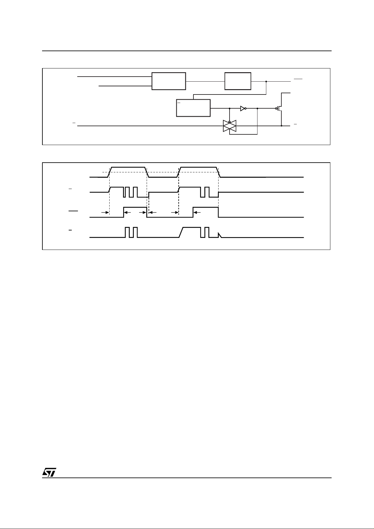
Figure 12. Chip-Enable Gating
V
CC
V
RST
COMPARE
STM690A/692A/703/704/802/805/817/818/819
t
E
OUTPUT
CON
CONTROL
rec
Generator
RST
V
OUT
E
AI08802
Figure 13. Chip Enable Waveform
V
E
RST
E
CC
CON
V
RST
V
BAT
trec trec15µs
E
CON
AI08803b
11/37
STM690A/692A/703/704/802/805/817/818/819
Power-fail Input/Output (NOT available on STM818)
The Power-fail Input (PFI) is compared to an internal reference voltage (independent from the V
RST
comparator). If PFI is less than the power-fail
threshold (V
), the Power-Fail Output (PFO) will
PFI
go low. This function is intended for use as an undervoltage detector to signal a failing power supply. Typically PFI is connected through an external
voltage divider (see Figure 11. , pag e 8) to either
the unregulated DC input (if it is a vailable) or the
regulated output of the V
regulator. The voltage
CC
divider can be set up such that the voltage at PFI
falls below V
regulated V
several milliseconds before the
PFI
input to the STM690A/692A/703/
CC
704/802/805/817/818/819 Supervisor or the microprocessor drops below the m inimum o perating
voltage.
Figure 14. Power-fail Comparator Waveform (STM817/818/ 819)
V
CC
V
RST
During battery back-up, the power-fail comparator
turns off and PFO
ure 14 and Figure 15., page 13). This occurs after
drops below 2.4V (or VSO). When power re-
V
CC
turns, PFO
spec tiv e o f V
At the end of this time, the power-fail comparator
is enabled and PFO
is unused, PFI should be connected to V
left unconnected. PFO may be connec ted t o
PFO
on the STM703/704/818 so that a low voltage
MR
on PFI will generate a reset output.
Applications Information
These Supervisor circuits are not short-circuit protected. Shorting V
er-up transients such as charging a decoupling
capacitor - destroys the device. Decouple both
and V
V
CC
pacitors as close to the device as possible.
goes (or remains) low (see Fig-
is forced high (STM817/819 only), irre-
for the WRITE protect time (t
PFI
rec
follows PFI. If the comparator
and
SS
to ground - excluding pow-
OUT
pins to ground by placing 0.1µF ca-
BAT
).
VSO (or 2.4V)
PFO
(STM817/819)
RST
(STM818)
E
CON
trec
PFO follows PFI PFO follows PFI
RST to E
Delay (STM818)
CON
AI08804a
12/37

STM690A/692A/703/704/802/805/817/818/819
Figure 15. Power-fail Comparator Waveform (STM690A/692A/ 703 /704 /802/80 5)
V
CC
V
RST
2.4V (or V
PFO
RST
)
SO
PFO follows PFI PFO follows PFI
trec
AI08832a
13/37

STM690A/692A/703/704/802/805/817/818/819
Using a SuperCap™ as a Backup Power Source
SuperCaps™ are capac itors with extremely high
capacitance values (e.g., order of 0.47F) for their
size. Figure 16 shows how to use a SuperCap as
a back-up power sou rce. The SuperCap m ay be
connected through a diode to the 5V input. Since
can exceed VCC while VCC is above the reset
V
BAT
threshold, there are no special precautions when
using these supervisors with a SuperCap.
Negative-Going V
Transients
CC
The STM690A/692A/703/704/802/805/817/818/
819 Supervisor are relatively immune to negativegoing V
transients (glitches). Figure
CC
38., page 25 shows typical transient duration ver-
sus reset comparator overdrive (for which the
STM690A/692A/703/70 4/802/805/817/818/819
will NOT gener ate a reset pulse). The graph was
generated using a negative pulse a pplied to V
starting at V
+ 0.3V and ending below the reset
RST
CC
threshold by the magnitude indicated (comparator
overdrive). The graph indicates the maximum
pulse width a negative V
transient can have
CC
without causing a reset pulse. As the magnitude of
the transient increases (further below the threshold), the maximum allowable pulse width decreases. Any combination of duration and overdrive
which lies under the curve will NOT generate a reset signal. Typically, a V
transient that goes
CC
100mV below the reset threshold and lasts 40µs or
less will not cause a reset pu lse. A 0.1µF bypass
capacitor mounted as close as possible to the V
CC
pin provides additional transient immunity.
Battery Freshness Seal (STM817/818/819)
The battery freshness seal disconnects t he backup battery from internal circuitry and V
OUT
until it is
needed. This allows an OEM to ensure that the
back-up battery connected to V
will be fresh
BAT
when the final product is put to use. To enable the
freshness seal:
1. Connect a battery to V
2. Ground PFO
3. Bring V
;
above the reset threshold and hold
CC
BAT
;
it there until reset is deasserted following the
reset timeout period; and
4. Bring V
down again (Figure 17).
CC
Use the same procedure for the STM818, but
ground E
instead of PFO. Once the battery
CON
freshness seal is enabled (disconnecting the
back-up battery from internal circuitry and anything connected to V
is brought above V
V
CC
), it remains enabled until
OUT
.
RST
Figure 16. Using a SuperCap™
5V
V
V
,
CC
STMXXX
BAT
GND
V
OUT
RST
To external SRAM
To µP
Figure 17. Freshness Seal Enable Waveform
V
RST
V
CC
RST
(Externally held at 0V)
E
CON
(STM818)
(Externally held at 0V)
PFO
(STM817/819)
trec
out state latched
E
CON
at 1/2 t
rec
Seal enabled
PFO out state latched
at 1/2 t
rec
Seal Enabled
,
Freshness
,
Freshness
AI08805
AI08806
14/37

STM690A/692A/703/704/802/805/817/818/819
TYPICAL OPERATING CHARACTERISTICS
Note: Typical values are at TA = 25°C
Figure 18. V
Figure 19. V
-to-V
CC
5.0
4.0
3.0
On-Resistance (Ω)
2.0
OUT
-to-V
CC
1.0
V
0.0
–40 –20
-to-V
BAT
160
On-Resistance vs. Temperature
OUT
0 20 40 60 80 100 120
Temperature (°C)
On-Resistance vs. Temperature
OUT
VCC = 3.0V
VCC = 4.5V
VCC = 5.5V
AI10498
140
120
100
80
On-Resistance (Ω)
OUT
60
40
- to - V
BAT
20
V
0
–40 –20 0 20 40 60 80 100 120
V
V
V
V
BAT
BAT
BAT
BAT
Temperature (°C)
= 2.0V
= 3.0V
= 3.3V
= 3.6V
AI09140b
15/37

STM690A/692A/703/704/802/805/817/818/819
Figure 20. Supply Current vs. Temperature (no load )
30
25
20
15
10
Supply Current (µA)
5
0
–40 –20 0 20 40 60 80 100 120
Temperature (°C)
VCC = 2.7V
VCC = 3.0V
VCC = 3.6V
VCC = 4.5V
VCC = 5.5V
AI09141b
Figure 21. Battery Cu rrent vs. Temperature
1000
100
10
Battery Supply Current (nA)
1
0.1
–40 –20 0 20 40 60 80 100 120
V
= 2.0V
BAT
V
= 3.0V
BAT
V
= 3.6V
BAT
Temperature (°C)
AI10499
16/37

STM690A/692A/703/704/802/805/817/818/819
Figure 22. V
1.270
1.265
1.260
1.255
1.250
1.245
Threshold (V)
PFI
1.240
V
1.235
1.230
1.225
Threshold vs. Temperature
PFI
VCC = 3.0V
VCC = 4.5V
VCC = 4.75V
VCC = 5.5V
–40 –20 0 20 40 60 80 100 120
Temperature (°C)
AI09142c
Figure 23. Reset Comparator Propagation Delay vs. Temperature (Oth er than STM 817/818/ 819 )
30
28
26
24
22
20
18
16
Propagation Delay (µs)
14
12
10
–40 –20 0 20 40 60 80 100 120
Temperature (°C)
AI09143b
17/37

STM690A/692A/703/704/802/805/817/818/819
Figure 24. Reset Comparator Propagation Delay vs. Temperature (V
350
300
250
200
150
100
Propagation Delay (µs)
50
0
–40 –20 0 20 40 60 80 100 120
Temperature (°C)
Figure 25. Power-up t
240
vs. Temperature
rec
=3.0V; STM817/818/ 819)
BAT
1v/ms
10V/ms
AI11100
235
230
225
(ms)
rec
t
220
215
210
–40 –20 0 20 40 60 80 100 120
Temperature (°C)
VCC = 3.0V
VCC = 4.5V
VCC = 5.5V
AI09144b
18/37

STM690A/692A/703/704/802/805/817/818/819
Figure 26. Normalized Reset Threshold vs. Temperature
1.004
1.002
1.000
0.998
Normalized Reset Threshold
0.996
–40 –20 0 20 40 60 80 100 120
Temperature (°C)
Figure 27. Watchdog Time-out Period vs. Temperature
AI09145b
1.90
1.85
1.80
1.75
1.70
Watchdog Time-out Period (sec)
1.65
1.60
–40 –20 0 20 40 60 80 100 120
Temperature (°C)
VCC = 3.0V
VCC = 4.5V
VCC = 5.5V
AI09146b
19/37

STM690A/692A/703/704/802/805/817/818/819
Figure 28. E to E
60
50
40
30
CON
On-Resistance (Ω)
CON
20
E to E
10
0
–40 –20 0 20 40 60 80 100 120
Figure 29. PFI to PFO
4.0
On-Resistance vs. Temperature
Temperature (°C)
Propagation Delay vs. Temperature
VCC = 3.0V
VCC = 4.5V
VCC = 5.5V
AI09147b
VCC = 3.0V
3.0
2.0
1.0
VCC = 3.6V
VCC = 4.5V
VCC = 5.5V
PFI to PFO Propagation Delay (µs)
0.0
–40 –20 0 20 40 60 80 100 120
Temperature (°C)
AI09148b
20/37

STM690A/692A/703/704/802/805/817/818/819
Figure 30. Output Voltage vs. Load Current (VCC = 5V; V
5.00
4.98
(V)
OUT
V
4.96
4.94
0 1020304050
I
(mA)
OUT
Figure 31. Output Voltage vs. Load Current (V
2.80
= 0V; V
CC
= 2.8V; TA = 25°C)
BAT
= 2.8V; TA = 25°C)
BAT
AI10496
2.78
2.76
2.74
(V)
OUT
2.72
V
2.70
2.68
2.66
0.0 0.2 0.4 0.6 0.8 1.0
I
(mA)
OUT
AI10497
21/37

STM690A/692A/703/704/802/805/817/818/819
Figure 32. RST Output Voltage vs. Supply Voltage
5
4
3
(V)
RST
2
V
1
0
500ms/div
Figure 33. RS T Ou t put V ol ta ge vs . Su ppl y V ol ta ge
5
4
3
(V)
RST
2
V
V
V
V
RST
V
CC
RST
CC
AI09149b
5
4
3
(V)
CC
V
2
1
0
5
4
3
(V)
CC
2
V
1
0
500ms/div
1
0
AI09150b
22/37

Figure 34. RST Response Time (Assertion)
STM690A/692A/703/704/802/805/817/818/819
5V
V
CC
5V
RST
5µs/div
1V/div
4V
4V
1V/div
0V
AI09151b
23/37

STM690A/692A/703/704/802/805/817/818/819
Figure 35. RST Response Time (Assertion)
V
CC
1V/div
RST
1V/div
5V
4V
4V
0V
5µs/div
Figure 36. Power-fail Com parator Res ponse Time (Assertion)
5V
PFO
1.3V
PFI
AI09152b
1V/div
0V
500mV/div
24/37
500ns/div
0V
AI09153b

STM690A/692A/703/704/802/805/817/818/819
Figure 37. Power-fail Comparator Response Time (De-A ssertion )
5V
PFO
0V
PFI
0V
500ns/div
Figure 38. Maximum Transient Duration vs. Reset Thresh old Over drive
6000
5000
1V/div
1.3V
500mV/div
AI09154b
4000
Reset occurs
above the curve.
3000
2000
Transient Duration (µs)
1000
0
0.001 0.01 0.1 1 10
Reset Comparator Overdrive, V
– VCC (V)
RST
AI09156b
25/37

STM690A/692A/703/704/802/805/817/818/819
Figure 39. E to E
4.0
3.0
2.0
Propagation Delay (ns)
CON
1.0
E to E
0.0
–40 –20 0 20 40 60 80 100 120
Propagation Delay vs. Temperature
CON
Temperature (°C)
VCC = 3.0V
VCC = 4.5V
VCC = 5.5V
AI09157b
26/37

STM690A/692A/703/704/802/805/817/818/819
MAXIMUM RA T ING
Stressing the device above the rating l isted in t he
Absolute Maximum Ratings” table may cause permanent damage to the device. These are stress
ratings only and operation of the device at t hese or
any other conditions ab ove those i ndicated in t he
Operating sections of this specificat ion is not im-
Table 5. Absolute Maximum Ratings
Symbol Parameter Value Unit
plied. Exposure to Absolute Maximum Rating conditions for extended periods may affect device
reliability. Refer also to the STMicroelectronics
SURE Program and other relevan t quality documents.
T
STG
(1)
T
SLD
V
IO
V
CC/VBA T
I
O
P
D
Note: 1. Reflow at peak t em perature of 255°C to 260°C for < 3 0 seconds (total therma l budget not to exceed 180° C for between 90 to 150
seconds).
Storage Temperature (VCC Off)
Lead Solder Temperature for 10 seconds 260 °C
Input or Output Voltage
Supply Voltage –0.3 to 6.0 V
Output Current 20 mA
Power Dissipation 320 mW
–55 to 150 °C
–0.3 to V
CC
+0.3
V
DC AND AC PARAMETERS
This section summarizes t he operating m easurement conditions, and the DC and AC characteristics of the device. The parameters in the D C and
AC characteristics Tables that follow, are derived
from tests performed under the Measurement
Table 6. Operating and AC Measurement Conditions
Parameter
V
CC/VBA T
Ambient Operating Temperature (T
Input Rise and Fall Times ≤ 5ns
Supply Voltage
)
A
Conditions summarized in Table 6, Operating and
AC Measurement Conditions. Designers should
check that the operating cond itions in their circuit
match the operating conditions when relying on
the quoted parameters.
STM690A/692A/703/704/802/
805/817/818/819
1.0 to 5.5 V
–40 to 85 °C
Unit
Input Pulse Voltages
Input and Output Timing Ref. Voltages
0.2 to 0.8V
0.3 to 0.7V
CC
CC
V
V
27/37

STM690A/692A/703/704/802/805/817/818/819
Figure 40. E to ECON Propagation Delay Test Circuit
V
BAT
3.6V
25Ω Equivalent
Source Impedance
V
CC
V
CC
STMXXX
50
Ω
50Ω Cable
50
Ω
Note: 1. CL includes load capacit ance and scope probe capaci tance.
Figure 41. AC Tes ti ng Input/Outp ut Wav eforms
0.8V
CC
0.2V
CC
Figure 42. MR
Timing Waveform
MR
tMLRL
(1)
RST
E
E
CON
50pF C
(1)
L
GND
AI08854
0.7V
CC
0.3V
CC
AI02568
Note : 1. RST for ST M805.
Figure 43. Wat chdog Timin g
V
CC
RST
WDI
28/37
trec
tMLMH
trec
AI07837a
tWD
AI07891

Table 7. DC and AC Characteristics
LI
OL
OL
(2)
Alter-
native
Operating Voltage
Description
VCC Supply Current Excluding I
Supply Current in
V
CC
Battery Back-up Mode
V
Supply Current in
(4)
BA T
Battery Back-up Mode
V
Voltage (Active)
OUT
V
Voltage (Battery
OUT
Back-up)
to V
V
CC
V
to V
BA T
On-resistance
OUT
On-resistance
OUT
Input Leakage Current (MR)
Input Leakage Current (PFI)
Input Leakage Current
(6)
(WDI)
IH
IH
IL
IL
Input High Voltage (MR)
Input High Voltage (WDI)
Input Low Voltage (MR)
Input Low Voltage (WDI)
Output Low Voltage (PFO,
, RST)
RST
Output Low Voltage (E
Output Low Voltage (RST)
Sym
VCC,
V
BAT
I
BAT
V
V
V
V
I
CC
OUT1
OUT2
I
V
V
V
V
CON
STM690A/692A/703/704/802/805/817/818/819
Test Condition
T
= –40 to +85°C
A
OUT
Excluding I
V
Excluding I
I
OUT1
I
OUT2
I
OUT2
OUT
= 2.0V, MR = VCC)
CC
OUT
I
= 5mA
OUT1
I
= 75mA
OUT1
= 250µA, VCC > 2.5V
= 250µA, V
= 1mA, V
4.5V < V
0V = VIN = V
(1)
(VCC < 5.5V)
(V
= 2.3V,
BAT
(V
= 3.6V)
BA T
(5)
= 2.3V
BAT
= 2.3V
BAT
< 5.5V
CC
CC
WDI = VCC, time average
WDI = GND, time average –20 –15 µA
4.5V < V
V
(max) < VCC < 5.5V 0.7V
RST
4.5V < V
V
(max) < VCC < 5.5V 0.3V
RST
= V
V
CC
RST
< 5.5V
CC
< 5.5V
CC
(max), I
SINK
=
3.2mA
= V
BAT
RST
= V
(max),
CC
V
)
CC
I
= 1.6mA, E = 0V
OUT
I
= 50µA, VCC = 1.0V,
SINK
V
= VCC, TA = 0°C to 85°C
BA T
I
= 100µA, VCC = 1.2V,
SINK
V
Min Typ Max Unit
(3)
1.2
25 60 µA
25 35 µA
0.4 1.0 µA
(5)
VCC –
0.03
V
CC
0.3
VCC –
0.0015
V
BAT
0.1
–
–
VCC –
0.015
VCC –
0.15
VCC –
0.0006
V
BA T
0.034
V
BA T
–
–
0.14
34Ω
100 Ω
75 125 300 µA
–25 2 +25 nA
120 160 µA
2.0 V
CC
5.5 V
0.8 V
CC
0.3 V
0.2V
CC
0.3 V
0.3 V
V
V
V
V
V
V
V
V
29/37

STM690A/692A/703/704/802/805/817/818/819
Sym
Alter-
native
Description
Output High Voltage (RST,
RST)
V
OH
Output High Voltage (E
CON
)
Output High Voltage (PFO)
I
V
V
OH
Output High Voltage
I
VOH Battery Back-up (RST,
RST)
V
OHB
V
Battery Back-up (E
OH
CON
)
Power-fail Comparator (NOT available on STM818)
V
t
PFD
I
PFI
SC
PFI Input Threshold
PFI to PFO Propagation
Delay
PFO Output Short to
GND Current
PFI Falling
(V
Battery Switchover
RST
Power-down
)
Battery Back-up
V
SO
Switchover Voltage
(VCC < V
& VCC < V
BAT
(7,8)
Hysteresis 40 mV
Reset Thresholds
V
RST
Reset Threshold
(9)
Reset Threshold Hysteresis 25 mV
to RST Delay (from
V
CC
V
, VCC falling at 10V/ms)
RST
t
rec
RST Pulse Width 140 200 280 ms
Test Condition
I
VCC = V
V
CC
I
OUT
I
SOURCE
V
SOURCE
= VCC, TA = 0°C to 85°C
BA T
SOURCE
I
SOURCE
VCC = 0, V
I
SOURCE
VCC = 0, V
= 1mA,
SOURCE
= V
RST
RST
(max)
(max),
= 1.6mA, E = V
= 75µA,
= V
RST
(max)
CC
= 4µA, VCC = 1.1V,
= 4µA, VCC = 1.2V,
= V
V
BAT
CC
= 100µA,
= 2.8V
BAT
= 75µA,
= 2.8V
BAT
All other
CC
= 5V)
versions
STM802 1.225 1.250 1.275 V
(1)
CC
Min Typ Max Unit
2.4 V
0.8V
CC
0.8V
CC
0.8 V
0.9 V
0.8V
BA T
0.8V
BA T
1.20 1.25 1.30 V
2µs
= 5V, V
V
CC
Power-up
PFO
V
V
V
V
RST
RST
RST
RST
= 0V
> V
< V
> V
< V
BAT
BAT
BAT
BAT
0.10.752.0mA
V
BA T
V
RST
V
BA T
V
RST
STM690A/703, STM8XXL 4.50 4.65 4.75 V
STM692A/704, STM8XXM 4.25 4.40 4.50 V
STM817/818/819 100 µs
V
V
V
V
V
V
V
V
30/37

STM690A/692A/703/704/802/805/817/818/819
Sym
Alter-
native
Description
Test Condition
(1)
Min Typ Max Unit
Push-button Reset Input (STM703/704/819)
t
MLMH
t
MLRL
t
t
MRD
MR
MR Pulse Width
MR to RST Output Delay
Glitch Immunity STM819 100 ns
MR
MR
Pull-up Resistor
STM703/704 150 ns
STM819 1 µs
STM703/704 250 ns
STM819 120 ns
MR
= 0V, VCC = 5V
45 63 85 kΩ
Watchdog Timer (NOT available on STM703/704/819)
V
t
WD
Watchdog Timeout Period
WDI Pulse Width
(max) < VCC < 5.5V
RST
(max) < VCC < 5.5V
V
RST
1.12 1.60 2.24 s
50 ns
Chip-Enable Gating (STM818 only)
E
-to-E
E-to-E
Reset-to-E
E
CON
Note: 1. Valid for Ambient Operatin g T em perature : TA = –40 to 85°C; VCC = 4.75V to 5.5V for “L” versi ons; VCC = 4.5V to 5.5V for “M” ver-
sions; and V
2. V
supply current, logic input leakage, Watchdog functionality, Push-button Reset functionality, PFI functionality, state of RST and
CC
RST tested at V
can go to 0V if the other is greater than 2.0 V.
(min) = 1.0V for TA = 0°C to +85°C.
3. V
CC
4. Tested at V
5. Guaranteed by design.
6. WDI input is des igne d to be dr ive n by a thr ee-st ate ou tput device . To float WD I, the “h igh i mpe dance mode ” of the output de vice
must have a maximum leakage current of 10µA and a maximum output capacitance of 200pF. The output device must also be able
to source and sink at least 200µA when active.
7. When V
8. When V
9. For V
CC
BAT
RST
falling.
Resistance VCC = V
CON
Propagation Delay 4.5V < VCC < 5.5V
CON
High Delay
CON
V
Short Circuit Current
= 2.8V (except where not ed).
BAT
= 3.6V, and VCC = 5.5V. T he state of RST or R ST and PFO is tested at VCC = VCC (min). Either VCC or V
BAT
= 3.6V, VCC = 3.5V and 0V.
BAT
> VCC > V
> VCC > V
RST
BAT
, V
remains connected to VCC until VCC drops belo w V
OUT
, V
remains connected to VCC until VCC drops belo w t he battery voltage (V
OUT
CC
E
= Logic high, E
RST
(Power-down) 15 µs
= 5V, Disable Mode,
(max)
CON
= 0V
40 150 Ω
27ns
0.10.752.0mA
.
RST
) – 75mV.
BAT
BAT
31/37

STM690A/692A/703/704/802/805/817/818/819
PACKAG E MECHANICAL
Figure 44. SO8 – 8-lead Plastic Small Outline, 150 mils body width, Package Mech . Drawing
h x 45˚
A2
A
C
B
e
ddd
D
8
E
H
1
Note: Drawing is not to scale.
LA1 α
SO-A
Table 8. SO8 – 8-lead Plastic Small Outline, 150 mils body width, Package Mechanica l Data
Symb
Typ Min Max Typ Min Max
A – 1.35 1.75 – 0.053 0.069
mm inches
A1 – 0.10 0.25 – 0.004 0.010
B – 0.33 0.51 – 0.013 0.020
C – 0.19 0.25 – 0.007 0.010
D – 4.80 5.00 – 0.189 0.197
ddd– –0.10– –0.004
E – 3.80 4.00 – 0.150 0.157
e1.27– –0.050– –
H – 5.80 6.20 – 0.228 0.244
h – 0.25 0.50 – 0.010 0.020
L – 0.40 0.90 – 0.016 0.035
α –0°8°–0°8°
N8 8
32/37

STM690A/692A/703/704/802/805/817/818/819
Figure 45. TSSOP8 – 8-lead, Thin Shrink Small Outline, 3x3mm body size, Outline
D
8
1
5
EE1
4
α
A1
A2A
CP
eb
Note: Drawing is not to scale.
L
L1
TSSOP8BM
Table 9. TSSOP8 – 8-lead, Thin Shrink Small Outline, 3x3mm body size, Mechanical Data
Symb
Typ Min Max Typ Min Max
A – –1.10– –0.043
mm inches
c
A1 – 0.05 0.15 – 0.002 0.006
A2 0.85 0.75 0.95 0.034 0.030 0.037
b – 0.25 0.40 – 0.010 0.016
c – 0.13 0.23 – 0.005 0.009
CP – – 0.10 – – 0.004
D 3.00 2.90 3.10 0.118 0.114 0.122
e0.65– –0.026– –
E 4.90 4.65 5.15 0.193 0.183 0.203
E1 3.00 2.90 3.10 0.118 0.114 0.122
L 0.55 0.40 0.70 0.022 0.016 0.030
L1 0.95 – – 0.037 – –
α –0°6°–0°6°
N8 8
33/37

STM690A/692A/703/704/802/805/817/818/819
PART NUMBERING
Table 10. Ordering Information Scheme
Example: STM690A M 6 E
Device Type
STM690A/692A/703/704/802/805/817/818/819
Reset Threshold Voltage
STM690A/703: blank = V
STM8xxL: L = V
STM692A/704: blank = V
STM8xxM: M = V
Package
M = SO8
(1)
DS
= TSSOP8
= 4.50V to 4.75V
RST
RST
= 4.50V to 4.75V
RST
= 4.25V to 4.50V
RST
= 4.25V to 4.50V
Temperature Range
6 = –40 to 85°C
Shipping Method
E = Tubes
F = Tape & Reel
Note: 1. Contact local ST sales office for availability.
For other options, or for more information on any aspect of this device, please contact the ST Sales Office
nearest you.
34/37

Table 11. Marking Description
Part Number Reset Threshold Package Topside Marking
STM690A 4.65V SO8 690A
STM692A 4.65V SO8 692A
STM703 4.65V SO8 703
STM704 4.40V SO8 704
STM802L 4.65V SO8 802L
STM802M 4.40V SO8 802M
STM805L 4.65V SO8 805L
STM817L 4.65V
STM690A/692A/703/704/802/805/817/818/819
SO8
817L
TSSOP8
STM817M 4.40V
STM818L 4.65V
STM818M 4.40V
STM819L 4.65V
STM819M 4.40V
SO8
817M
TSSOP8
SO8
818L
TSSOP8
SO8
818M
TSSOP8
SO8
819L
TSSOP8
SO8
819M
TSSOP8
35/37

STM690A/692A/703/704/802/805/817/818/819
REVISION HISTORY
Table 12. Document Revision History
Date Version Revision Details
October 2003 1.0 First Issue
31-Oct-03 1.1 Update DC Characteristics (Table 7)
22-Dec-03 2.0
16-Jan-04 2.1
08-Apr-04 2.2 Update characteristics (Figure 13, 23, 29, 33, 34, 35, 38; Table 1,7)
25-May-04 3.0
05-Jul-04 4.0
29-Sep-04 5.0 Clarify root part numbers, pin descriptions (Figure 11, 13, 40; Table 7, 10)
Reformatted; updated characteristics (Figure 1, 3, 4, 7, 8, 9, 10, 11, 12, 13, 14, 15,
17; Table 3, 4, 7, 9, 11)
Add Typical Characteristics (Figure 19, 20, 22, 23, 25, 26, 27, 28, 29, 32, 33, 34,
35, 36, 37, 38, 39)
Remove references to ‘Open Drain’ (Figure 2, 5, 8; Table 2); update characteristics
(Table 3, 7)
Update package availability, pin description; promote document (Figure 1, 14, 15;
Table 3. 7, 10)
01-Mar-05 6.0
Update characteristics (Figure 18, 19, 20, 21, 22, 23, 24, 25, 26, 27, 28, 29, 30, 31,
32, 33, 34, 35, 36, 37, 38, 39)
36/37

STM690A/692A/703/704/802/805/817/818/819
Information furnished is believed to be accurate and reliable. However, STMicroelectronics a ssumes no responsibility fo r the c onsequences
of use of such information nor for any infringement of patents or other rights of third parties which may result from its use. No license is granted
by implication or otherwise under any patent or patent rights of STMicroelectronics. Specifications mentioned in this publication are subject
to change without notice. This publication supersedes and replaces all information previously supplied. STMicroelectronics products are not
authori zed for use as crit i cal compon ent s in life support devices or sy stems with out express wr i tten approval of STMicroel ectronics.
The ST logo is a registered trademark of STMi croelectr onics.
All other nam es are the pro perty of their respective owners
© 2005 STMi croelectro ni cs - All rights reserved
Australi a - Belgium - B razil - Canad a - China - Czech Republic - Fi nl and - Franc e - Germany - Hong Kong - Ind ia - Is rael - Italy - Japan -
Malaysia - M al ta - Morocco - Singapore - Spain - Swed en - Switze rl and - United K ingdom - Uni ted States of America
STMicroelectronic s group of companies
www.st.com
37/37
 Loading...