

Page 1

AN5406
Application note
How to build a LoRa
®
application with STM32CubeWL
Introduction
This application note guides the user through all the steps required to build specific LoRa® applications based on
STM32WL Series microcontrollers.
LoRa® is a type of wireless telecommunication network designed to allow long-range communications at a very‑low bitrate
and to enable long-life battery-operated sensors. LoRaWAN® defines the communication and security protocol that ensures the
interoperability with the LoRa® network.
The firmware in the STM32CubeWL MCU Package is compliant with the LoRa Alliance® specification protocol named
LoRaWAN® and has the following main features:
• Application integration ready
•
Easy add-on of the low-power LoRa® solution
• Extremely low CPU load
• No latency requirements
• Small STM32 memory footprint
• Low-power timing services
The firmware of the STM32CubeWL MCU Package is based on the STM32Cube HAL drivers.
This document provides customer application examples on the STM32WL Nucleo-64 boards NUCLEO_WL55JC
(order codes NUCLEO‑WL55JC1 for high‑frequency band and NUCLEO-WL55JC2 for low-frequency band).
To fully benefit from the information in this application note and to create an application, the user must be familiar with the
STM32 microcontrollers, the LoRa® technology, and understand system services such as low-power management and task
sequencing.
AN5406 - Rev 4 - February 2021
For further information contact your local STMicroelectronics sales office.
www.st.com
Page 2
1 Overview
The STM32CubeWL runs on STM32WL Series microcontrollers based on the Arm® Cortex®-M processor.
Note: Arm is a registered trademark of Arm Limited (or its subsidiaries) in the US and/or elsewhere.
1.1 Acronyms
Table 1. Acronyms
Acronym Definition
ABP Activation by personalization
ADR Adaptive data rate
BSP Board support package
HAL Hardware abstraction layer
LoRa Long range radio technology
LoRaWAN LoRa wide-area network
LPWAN Low-power wide-area network
MAC Media access control
MCPS MAC common part sublayer
MIB MAC information base
MLME MAC sublayer management entity
MSC Message sequence chart
<target> STM32WL Nucleo-64 boards (NUCLEO-WL55JC)
AN5406
Overview
1.2 Reference documents
[1] User manual STM32 LoRa Expansion Package for STM32Cube (UM2073)
[2] STM32WLEx reference manual (RM0461)
[3] Application note LoRaWAN AT commands for STM32CubeWL (AN5481)
[4] Application note Building wireless applications with STM32WB Series microcontrollers (AN5289)
[5] IEEE Std 802.15.4TM - 2011. Low-Rate Wireless Personal Area Networks (LR-WPANs)
1.3 LoRa standard
Refer to document [1] for more details on LoRa and LoRaWAN recommendations.
AN5406 - Rev 4
page 2/63
Page 3

2 STM32CubeWL architecture
2.1 STM32CubeWL overview
The firmware of the STM32CubeWL MCU Package includes the following resources (see Figure 1):
• Board support package: STM32WLxx_Nucleo drivers
• STM32WLxx_HAL_Driver
• Middleware:
– LoRaWAN containing:
◦ LoRaWAN layer
◦ LoRa utilities
◦ LoRa software crypto engine
◦ LoRa state machine
– SubGHz_Phy layer middleware containing the radio and radio_driver interfaces
• LoRaWAN applications:
– AT_Slave
– End_Node
• SubGHz_Phy application:
– PingPong
In addition, this application provides efficient system integration with the following:
• a sequencer to execute the tasks in background and enter low-power mode when there is no activity
• a timer server to provide virtual timers running on RTC (in Stop and Standby modes) to the application
For more details refer to Section 7 Utilities description.
AN5406
STM32CubeWL architecture
AN5406 - Rev 4
page 3/63
Page 4
Figure 1. Project file structure
BSP drivers for STM32WL Nucleo-64 board
STM32WL HAL drivers
Middleware LoRa crypto engine
Middleware LoRa state machine
Middleware LoRa MAC layer
Middleware LoRa utilities
Middleware SubGHz_Phy
AN5406
STM32CubeWL overview
LoRaWAN AT_Slave application
LoRaWAN End_Node application
SubGhz_Phy PingPong application
AN5406 - Rev 4
page 4/63
Page 5
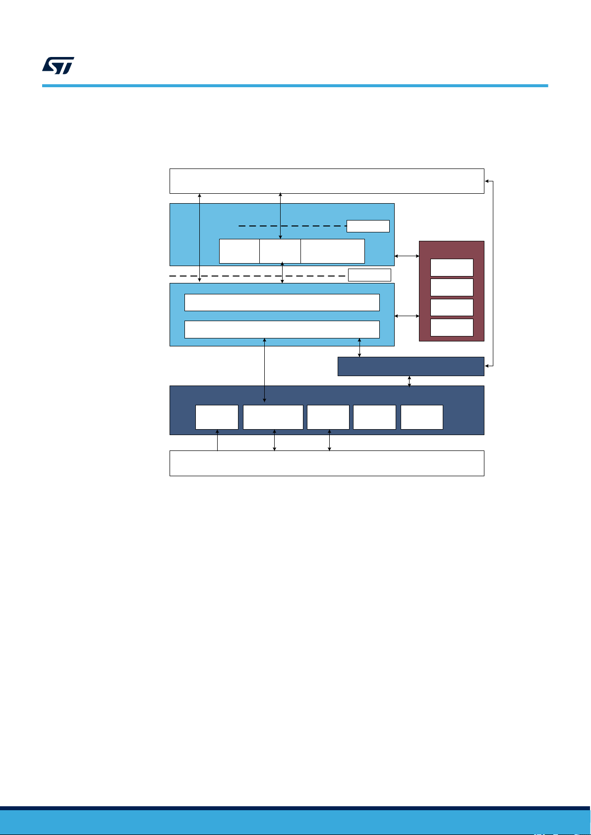
2.2 Static LoRa architecture
The figure below describes the main design of the firmware for the LoRa application.
AN5406
Static LoRa architecture
Figure 2. Static LoRa architecture
LoRa application
(AT_Slave, End_Node or PingPong)
LoRaWAN middleware
LmHandler.h
LmHandler LoRaMAC LoRaMAC crypto
radio.h
SubGHz_Phy middleware
radio.c
radio_driver.c
Utilities
Timer server
Sequencer
Debug trace
Low-power
mode
Board support package (BSP)
Hardware abstraction layer APIs (HAL)
NVIC SubGHz RCC GPIO RTC
Sub-GHz radio system peripheral
The HAL uses STM32Cube APIs to drive the MCU hardware required by the application. Only specific hardware
is included in the LoRa middleware as it is mandatory to run a LoRa application.
The RTC provides a centralized time unit that continues to run even in low-power mode (Stop 2 mode). The RTC
alarm is used to wake up the system at specific timings managed by the timer server.
The radio driver uses the SubGHz HAL to control the radio (see the above figure). The radio driver also provides
a set of APIs to be used by higher-level software.
The radio driver is split in the following parts:
• radio.c: contains all functions that are radio dependent only.
• radio_driver.c: contains low-level radio drivers.
AN5406 - Rev 4
The MAC controls the SubGHz_Phy using the 802.15.4 model. The MAC interfaces with the SubGHz_Phy driver
and uses the timer server to add or remove timed tasks.
Since the state machine that controls the LoRa Class A, is sensitive, an intermediate level of software is inserted
(lora.c) between the MAC and the application (refer to LoRaMAC driver in the above figure). With a limited set
of APIs, the user is free to implement the Class A state machine at application level. For more details, refer to
Section 6 .
The application, built around an infinite loop, manages the low-power, runs the interrupt handlers (alarm or GPIO)
and calls the LoRa Class A if any task must be done.
page 5/63
Page 6
2.3 Dynamic view
The MSC (message sequence chart) shown in the figure below depicts a Class A device transmitting an
application data and receiving application data from the server.
Figure 3. Class A Tx and Rx processing MSC
CPU Sub-GHz
LoRaApp
LmHandler
LmHandlerSend
status status status
OnMacProcessNotify
_LmHandler
Packages
Process
OnTxdata McpsConfirm
LoRaMacMcps
Request
LoRaMacProcess
LoRaMAC
OnRadioTxDone
Radio Timer
RadioSend
setRxwindow1
TimerIsr
RadioRx
AN5406
Dynamic view
radio
peripheral
Tx
RadioIsr
OnMacProcessNotify
_LmHandler
Packages
Process
OnRxdata
OnRadioRxDone
LoRaMacProcess
McpsIndication
RadioIsr
Once the radio has completed the application data transmission, an asynchronous RadioIRQ wakes up the
system. The RadioIsr here calls txDone in the handler mode.
All RadioIsr and MAC timer call a LoRaMacProcessNotify callback to request the application layer to update
the LoRaMAC state and to do further processing when needed.
For instance, at the end of the reception, rxDone is called in the ISR (handler), but all the Rx packet processing
including decryption must not be processed in the ISR. This case is an example of call sequence. If no data is
received into the Rx1 window, then another Rx2 window is launched..
Rx
AN5406 - Rev 4
page 6/63
Page 7

3 SubGHz HAL driver
This section focuses on the SubGHz HAL (other HAL functions such as timers or GPIO are not detailed).
The SubGHz HAL is directly on top of the sub-GHz radio peripheral (see Figure 2. Static LoRa architecture).
The SubGHz HAL driver is based on a simple one-shot command-oriented architecture (no complete processes).
Therefore, no LL driver is defined.
This SubGHz HAL driver is composed the following main parts:
• Handle, initialization and configuration data structures
• Initialization APIs
• Configuration and control APIs
• MSP and events callbacks
• Bus I/O operation based on the SUBGHZ_SPI (Intrinsic services)
As the HAL APIs are mainly based on the bus services to send commands in one-shot operations, no functional
state machine is used except the RESET/READY HAL states.
3.1 SubGHz resources
The following HAL SubGHz APIs are called at the initialization of the radio:
• Declare a SUBGHZ_HandleTypeDef handle structure.
• Initialize the sub-GHz radio peripheral by calling the HAL_SUBGHZ_Init(&hUserSubghz) API.
• Initialize the SubGHz low-level resources by implementing the HAL_SUBGHZ_MspInit() API:
– PWR configuration: Enable wakeup signal of the sub-GHz radio peripheral.
– NVIC configuration:
◦ Enable the NVIC radio IRQ interrupts.
◦ Configure the sub-GHz radio interrupt priority.
The following HAL radio interrupt is called in the stm32wlxx_it.c file:
• HAL_SUBGHZ_IRQHandler in the SUBGHZ_Radio_IRQHandler.
AN5406
SubGHz HAL driver
3.2 SubGHz data transfers
The Set command operation is performed in polling mode with the HAL_SUBGHZ_ExecSetCmd(); API.
The Get Status operation is performed using polling mode with the HAL_SUBGHZ_ExecGetCmd(); API.
The read/write register accesses are performed in polling mode with following APIs:
• HAL_SUBGHZ_WriteRegister();
• HAL_SUBGHZ_ReadRegister();
• HAL_SUBGHZ_WriteRegisters();
• HAL_SUBGHZ_ReadRegisters();
• HAL_SUBGHZ_WriteBuffer();
• HAL_SUBGHZ_ReadBuffer();
AN5406 - Rev 4
page 7/63
Page 8
BSP STM32WL Nucleo-64 boards
4 BSP STM32WL Nucleo-64 boards
This BSP driver provides a set of functions to manage:
• an application dependent part, implementing external control of on-board components: RF switches, TCXO,
RF losses and LEDs/sensors available on the STM32WL Nucleo-64 board (NUCLEO-WL55JC)
• a fixed part implementing the internal radio accesses (reset, busy and the NVIC radio IRQs)
Note: In the current implementation, due to STM32CubeMX limitation, the firmware does not use BSP files but
radio_board_if.c/.h for radio related items, and board_resources.c/.h for LED and push buttons. The
choice between the two implementations is done into Core/Inc/platform.h by selecting USE_BSP_DRIVER
or MX_BOARD_PSEUDODRIVER.
4.1 Frequency band
Two types of Nucleo board are available on the STM32WL Series:
• NUCLEO-WL55JC1: high-frequency band, tuned for frequency between 865 MHz and 930 MHz
• NUCLEO-WL55JC2: low-frequency band, tuned for frequency between 470 MHz and 520 MHz
Obviously, If the user tries to run a firmware compiled at 868 MHz on a low-frequency band board, very poor RF
performances are expected.
The firmware does not check the band of the board on which it runs.
AN5406
4.2 RF switch
The STM32WL Nucleo-64 board embeds an RF 3-port switch (SP3T) to address, with the same board, the
following modes:
• high-power transmission
• low-power transmission
• reception
int32_t BSP_RADIO_Init(void)
BSP_RADIO_ConfigRFSwitch(BSP_RADIO_Switch_TypeDef Config)
int32_t BSP_RADIO_DeInit (void)
int32_t BSP_RADIO_GetTxConfig(void)
The RF states versus the switch configuration are given in the table below.
RF state
High-power transmission Low High High
Low-power transmission High High High
Reception High Low High
Table 2. BSP radio switch
Function Description
Initializes the RF switch.
Configures the radio switch.
De-initializes the RF switch.
Returns the board configuration:
high power, low power or both.
Table 3. RF states versus switch configuration
FE_CTRL1 FE_CTRL2 FE_CTRL3
AN5406 - Rev 4
page 8/63
Page 9
4.3 RF wakeup time
The sub-GHz radio wakeup time is recovered with the following API.
uint32_t BSP_RADIO_GetWakeUpTime(void)
The user must start the TCXO by setting the command RADIO_SET_TCXOMODE with a timeout depending of the
application.
The timeout value can be updated in stm32wlxx_nucleo_conf.h. Default template value is defined below.
#define RF_WAKEUP_TIME 10U
4.4 TCXO
Various oscillator types can be mounted on the user application. On the STM32WL Nucleo-64 boards, a TCXO
(temperature compensated crystal oscillator) is used to achieve a better frequency accuracy.
AN5406
RF wakeup time
Table 4. BSP radio wakeup time
Function Description
Returns RF_WAKEUP_TIME value.
uint32_t BSP_RADIO_IsTCXO (void)
The user can change this value in stm32wlxx_nucleo_conf.h:
#define IS_TCXO_SUPPORTED 1U
4.5 Power regulation
Depending on the user application, a LDO or an SMPS (also named DCDC) is used for power regulation.
An SMPS is used on the STM32WL Nucleo-64 boards.
uint32_t BSP_RADIO_IsDCDC (void)
The user can change this value in stm32wlxx_nucleo_conf.h:
#define IS_DCDC_SUPPORTED 1U
The SMPS on the board can be disabled by setting IS_DCDC_SUPPORTED to 0.
Table 5. BSP radio TCXO
Function Description
Returns IS_TCXO_SUPPORTED value.
Table 6. BSP radio SMPS
Function Description
Returns IS_DCDC_SUPPORTED value.
AN5406 - Rev 4
page 9/63
Page 10
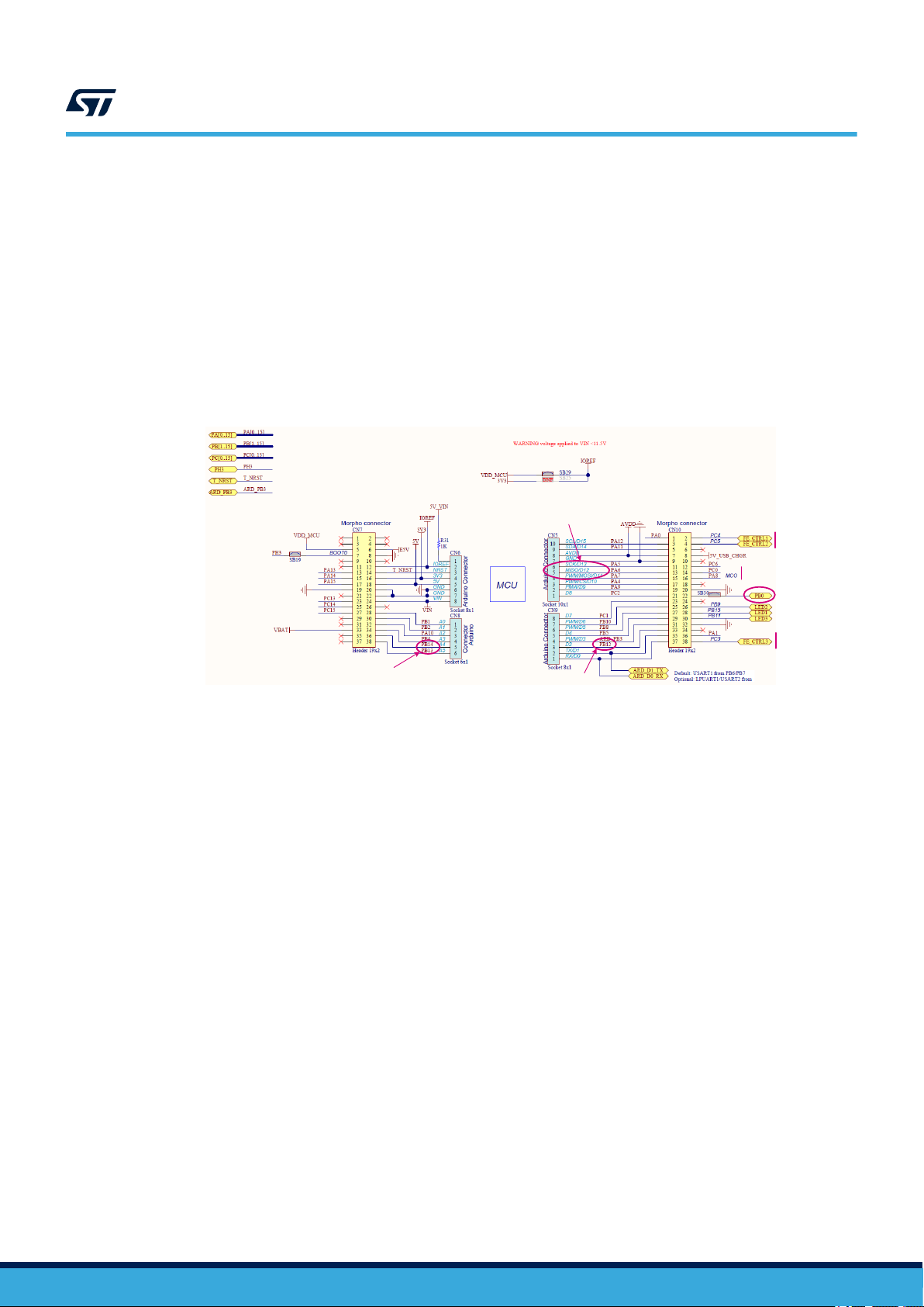
4.6 STM32WL Nucleo-64 board schematic
The figure below details the STM32WL Nucleo-64 board, MB1389 reference board schematic, highlighting some
useful signals:
• control switches on PC4, PC5 and PC3
• TCXO control voltage PIN on PB0
• debug lines on PB12, PB13 and PB14
• system clock on PA8
• SCK on PA5
• MISO on PA6
• MOSI on PA7
Figure 4. NUCLEO-WL55JC schematic
Data transaction:
SKC, MOSI, MISO
AN5406
STM32WL Nucleo-64 board schematic
Control switchs
1 and 2
Debug line 2 and 3
Debug line 1
System clock
TCXO control
voltage
Control
switch 3
AN5406 - Rev 4
page 10/63
Page 11

5 SubGHz_Phy layer middleware description
The radio abstraction layer is composed of two layers:
• high-level layer (radio.c)
It provides a high-level radio interface to the stack middleware. It also maintains radio states, processes
interrupts and manages timeouts. It records callbacks and calls them when radio events occur.
• low-level radio drivers
It is an abstraction layer to the RF interface. This layer knows about the register name and structure, as well
as detailed sequence. It is not aware about hardware interface.
The SubGHz_Phy layer middleware contains the radio abstraction layer that interfaces directly on top of the
hardware interface provided by BSP (refer Section 4 BSP STM32WL Nucleo-64 boards).
The SubGHz_Phy middleware directory is divided in two parts
• radio.c: contains a set of all radio generic callbacks, calling radio_driver functions. This set of APIs is
meant to be generic and identical for all radios.
• radio_driver.c: low-level radio drivers
AN5406
SubGHz_Phy layer middleware description
AN5406 - Rev 4
page 11/63
Page 12

5.1 Middleware radio driver structure
A radio generic structure, struct Radio_s Radio {};, is defined to register all the callbacks, with the fields detailed in
the table below.
Table 7. Radio_s structure callbacks
Callback Description
RadioInit
RadioGetStatus
RadioSetModem
RadioSetChannel
RadioIsChannelFree
RadioRandom
RadioSetRxConfig
RadioSetTxConfig
RadioCheckRfFrequenc
RadioTimeOnAir
RadioSend
RadioSleep
RadioStandby
RadioRx
RadioStartCad
RadioSetTxContinuousWave
RadioRssi
RadioWrite
RadioRead
RadioSetMaxPayloadLength
RadioSetPublicNetwork
RadioGetWakeUpTime
RadioIrqProcess
RadioRxBoosted
RadioSetRxDutyCycle
RadioTxPrbs
RadioTxCw
Initializes the radio.
Returns the current radio status.
Configures the radio with the given modem.
Sets the channel frequency.
Checks if the channel is free for the given time.
Generates a 32-bit random value based on the RSSI readings.
Sets the reception parameters.
Sets the transmission parameters.
Checks if the given RF frequency is supported by the hardware.
Computes the packet time on air in ms, for the given payload.
Sends the buffer of size. Prepares the packet to be sent and sets the radio in
transmission.
Sets the radio in Sleep mode.
Sets the radio in Standby mode.
Sets the radio in reception mode for the given time.
Starts a CAD (channel activity detection).
Sets the radio in continuous wave transmission mode.
Reads the current RSSI value.
Writes the radio register at the specified address.
Reads the radio register at the specified address.
Sets the maximum payload length.
Sets the network to public or private. Updates the sync byte.
Gets the time required for the board plus radio to exit Sleep mode.
Processes radio IRQ.
Sets the radio in reception mode with max LNA gain for the given time.
Sets the Rx duty-cycle management parameters.
Sets the transmitter in continuous PRBS mode.
Sets the transmitter in continuous unmodulated carrier mode.
AN5406
Middleware radio driver structure
AN5406 - Rev 4
page 12/63
Page 13

5.2 Radio IRQ interrupts
The possible sub-GHz radio interrupt sources are detailed in the table below.
Bit Source Description Packet type Operation
txDone
0
rxDone
1
PreambleDetected
2
SyncDetected
3
HeaderValid
4
HeaderErr
5
Err
6
CrcErr
CadDone
CadDetected
8
Timeout
9
Radio IRQ interrupts
Table 8. Radio IRQ bit mapping and definition
Packet transmission finished
Packet reception finished
Preamble detected
Synchronization word valid GFSK
Header valid
Header error
Preamble, sync word, address, CRC or
length error
CRC error
Channel activity detection finished
Channel activity detected
Rx or TX timeout LoRa and GFSK Rx and Tx
LoRa and GFSK
LoRa
GFSK
LoRa7
AN5406
Tx
Rx
CAD
For more details, refer to the product reference manual.
AN5406 - Rev 4
page 13/63
Page 14

6 LoRaWAN middleware description
The LoRa stack middleware is split into the following modules:
• LoRaMAC layer module (in Middlewares\Third_Party\LoRaWAN\Mac)
• LoRa utilities module (in Middlewares\Third_Party\LoRaWAN\Utilities)
• LoRa crypto module (in Middlewares\Third_Party\LoRaWAN\Crypto)
• LoRa LmHandler module (in Middlewares\Third_Party\LoRaWAN\LmHandler)
6.1 LoRaWAN middleware features
• Compliant with the specification for the LoRa Alliance protocol, named LoRaWAN
• On-board LoRaWAN Class A, Class B and Class C protocol stack
• EU 868MHz ISM band ETSI compliant
• EU 433MHz ISM band ETSI compliant
• US 915MHz ISM band FCC compliant
• KR 920Mhz ISM band defined by Korean government
• RU 864Mhz ISM band defined by Russian regulation
• CN 779Mhz and CN470Mhz ISM bands defined by Chinese government
• AS 923Mhz ISM band defined by Asian governments
• AU 915Mhz ISM bands defined by Australian government
• IN 865Mhz ISM bands defined by Indian government
• End-device activation either through OTAA or through activation-by-personalization (ABP)
• Adaptive data rate support
• LoRaWAN test application for certification tests included
• Low-power optimized
AN5406
LoRaWAN middleware description
6.2 LoRaWAN middleware initialization
The initialization of the LoRaMAC layer is done through the LoRaMacInitialization API, that initializes both
the preamble run time of the LoRaMAC layer and the callback primitives of the MCPS and MLME services (see
the table below).
Table 9. LoRaWAN middleware initialization
Function Description
LoRaMacStatus_t LoRaMacInitialization
(LoRAMacPrimitives_t *primitives,
LoRaMacCallback_t *callback,
LoRaMacRegion_t region)
6.3 Middleware MAC layer APIs
The provided APIs follow the definition of “primitive” defined in IEEE802.15.4-2011 (see document [5]).
The interfacing with the LoRaMAC is made through the request-confirm and the indication-response architecture.
The application layer can perform a request that the LoRaMAC layer confirms with a confirm primitive.
Conversely, the LoRaMAC layer notifies an application layer with the indication primitive in case of any event.
The application layer may respond to an indication with the response primitive. Therefore, all the confirm or
indication are implemented using callbacks.
Initializes the LoRaMAc layer module
(see Section 6.4 Middleware MAC layer callbacks)
AN5406 - Rev 4
page 14/63
Page 15

Middleware MAC layer APIs
The LoRaMAC layer provides the following services:
• MCPS services
In general, the LoRaMAC layer uses the MCPS services for data transmissions and data receptions.
Table 10. MCPS services
Function Description
LoRaMacStatus_t LoRaMacMcpsRequest
(McpsReq_t *mcpsRequest)
Requests to send Tx data.
• MLME services
The LoRaMAC layer uses the MLME services to manage the LoRaWAN network.
Table 11. MMLE services
Function Description
LoRaMacStatus_t LoRaMacMlmeRequest
(MlmeReq_t *mlmeRequest )
Generates a join request or requests for a link check.
AN5406
• MIB services
The MIB stores important runtime information (such as MIB_NETWORK_ACTIVATION or MIB_NET_ID) and
holds the configuration of the LoRaMAC layer (for example the MIB_ADR, MIB_APP_KEY).
Table 12. MIB services
Function
LoRaMacStatus_t LoRaMacMibSetRequestConfirm
(MibRequestConfirm_t *mibSet)
LoRaMacStatus_t LoRaMacMibGetRequestConfirm
(MibRequestConfirm_t *mibGet )
Sets attributes of the LoRaMAC layer.
Gets attributes of the LoRaMAC layer.
Description
AN5406 - Rev 4
page 15/63
Page 16
6.4 Middleware MAC layer callbacks
The LoRaMAC user event functions primitives (also named callbacks) to be implemented by the application are
the following:
• MCPS
Function Description
void (*MacMcpsConfirm )
(McpsConfirm_t *McpsConfirm)
Void (*MacMcpsIndication)
(McpsIndication_t *McpsIndication)
• MLME
Function Description
void ( *MacMlmeConfirm )
( MlmeConfirm_t *MlmeConfirm )
AN5406
Middleware MAC layer callbacks
Table 13. MCPS primitives
Response to a McpsRequest
Notifies the application that a received packet is available.
Table 14. MLME primitive
Manages the LoRaWAN network.
6.5
• MIB
No available functions.
Middleware MAC layer timers
• Delay Rx window
Refer to document [1], section 'End-device classes' for more details.
Table 15. Delay Rx window
Function Description
void OnRxWindow1TimerEvent (void)
void OnRxWindow2TimerEvent (void)
• Delay for Tx frame transmission
Table 16. Delay for Tx frame transmission
Function Description
void OnTxDelayedTimerEvent (void)
Sets the RxDelay1
(ReceiveDelayX - RADIO_WAKEUP_TIME).
Sets the RxDelay2.
Sets the timer for Tx frame transmission.
AN5406 - Rev 4
page 16/63
Page 17

• Delay for Rx frame
Table 17. Delay for Rx frame
Function Description
void OnAckTimeoutTimerEvent (void)
Sets timeout for received frame acknowledgment.
6.6 Middleware LmHandler application function
The interface to the MAC is done through the MAC interface LoRaMac.h file, in one of the following modes:
• Standard mode
An interface file (LoRaMAC driver, see Figure 2 ) is provided to let the user start without worrying about the
LoRa state machine. This file is located in
Middlewares\Third_Party\LoRaWAN\LmHandler\LmHandler.c and implements:
– a set of APIs to access to the LoRaMAC services
– the LoRa certification test cases that are not visible to the application layer
• Advanced mode
The user accesses directly the MAC layer by including the MAC in the user file.
AN5406
Middleware LmHandler application function
AN5406 - Rev 4
page 17/63
Page 18
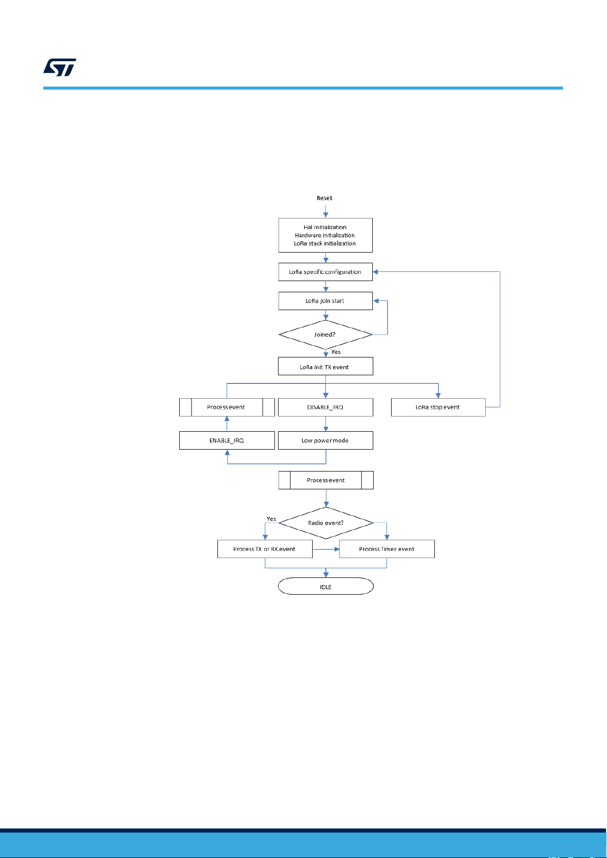
6.6.1 Operation model
The operation model proposed for the LoRa End_Node is based on ‘event-driven’ paradigms including ‘timedriven’ (see the figure below). The behavior of the LoRa system is triggered either by a timer event or by a radio
event plus a guard transition.
AN5406
Middleware LmHandler application function
Figure 5. Operation model
AN5406 - Rev 4
The next sections detail the End_Node and AT_Slave APIs used to access the LoRaMAC services. The
corresponding interface files are located in:
Middlewares\Third_Party\LoRaWAN\LmHandler\LmHandler.c
The user must implement the application with these APIs.
An example of End_Node application is provided in
\Projects\<target>\Applications\LoRaWAN\End_Node\LoRaWAN\App\lora_app.c.
An example of AT_Slave application is provided in
\Projects\<target>\Applications\LoRaWAN\AT_Slave\LoRaWAN\App\lora_app.c.
page 18/63
Page 19

6.6.2 Main application functions definition
Function Description
LmHandlerErrorStatus_t LmHandlerInit
(LmHandlerCallbacks_t *handlerCallbacks)
Table 19. LoRa configuration
Function Description
LmHandlerErrorStatus_t LmHandlerConfigure
(LmHandlerParams_t *handlerParams)
Table 20. LoRa End_Node join request entry point
Function Description
void LmHandlerJoin (ActivationType_t mode)
AN5406
Middleware LmHandler application function
Table 18. LoRa initialization
Initialization of the LoRa finite state machine
Configuration of all applicative parameters
Join request to a network either in OTAA mode or
ABP mode.
Table 21. LoRa stop
Function
void LmHandlerStop (void)
Table 22. LoRa request class
Function
LmHandlerErrorStatus LmHandlerRequestClass
(DeviceClass_t newClass)
Table 23. Send an uplink frame
Function
LmHandlerErrorStatus_t LmHandlerSend
(LmHandlerAppData_t *appData,
LmHandlerMsgTypes_t isTxConfirmed)
TimerTime_t *nextTxIn, bool allowDelayedTx)
Description
Stops the LoRa process and waits a new configuration
before a rejoin action.
Description
Requests the MAC layer to change LoRaWAN
class.
Description
Sends an uplink frame. This frame can be either
an unconfirmed empty frame or an unconfirmed/
confirmed payload frame.
AN5406 - Rev 4
page 19/63
Page 20

6.7 Application callbacks
Callbacks in the tables below are used for both End_Node and AT_Slave applications.
Function Description
uint8_t GetBatteryLevel (void)
Function Description
uint16_t GetTemperature (void)
AN5406
Application callbacks
Table 24. Current battery level
Gets the battery level.
Table 25. Current temperature
Gets the current temperature (in °C) of the device in
q7.8 format.
Table 26.
Function Description
LmHandler process
void (*OnMacProcess)(void)
Table 27. Join status
Function
void OnJoinRequest (LmHandlerJoinParams_t
*joinParams)
Table 28. Tx frame done
Function
void OnTxData (LmHandlerTxParams_t *params)
Table 29. Rx frame received
Function
void OnRxData ( LmHandlerAppData_t *appData,
LmHandlerRxParams_t *params)
Calls LmHandler Process when a Radio IRQ is
received.
Description
Notifies the upper layer that a network has been
joined.
Description
Notifies the upper layer that a frame has been
transmitted
Description
Notifies the upper layer that an applicative frame has
been received.
AN5406 - Rev 4
page 20/63
Page 21

6.8 Extended application functions
These callbacks are used for both LoRaWAN_End-Node and LoRaWAN_AT-Slave applications.
Table 30. Getter/setter functions
Function Description
int32_t LmHandlerGetCurrentClass( DeviceClass_T
*deviceClass)
int32_t LmHandlerGetDevEUI( uint8_t *devEUI)
int32_t LmHandlerSetDevEUI( uint8_t *devEUI)
int32_t LmHandlerGetAppEUI( uint8_t *appEUI)
int32_t LmHandlerSetAppEUI( uint8_t *appEUI)
int32_t LmHandlerGetAppKey( uint8_t *appKey)
int32_t LmHandlerSetAppKey( uint8_t *appKey)
int32_t LmHandlerGetNetworkID( uint32_t *networkId)
int32_t LmHandlerSetNetworkID uint32_t networkId)
int32_t LmHandlerGetDevAddr( uint32_t *devAddr)
int32_t LmHandlerSetDevAddr( uint32_t devAddr)
int32_t LmHandlerSetNwkSKey( uint8_t *nwkSKey)
int32_t LmHandlerSetAppSKey( uint8_t *appSKey)
int32_t LmHandlerGetActiveRegion( LoRaMacRegion_t *region)
int32_t LmHandlerSetActiveRegion( LoRaMacRegion_t region)
int32_t LmHandlerGetAdrEnable( bool *adrEnable)
int32_t LmHandlerSetAdrEnable( bool adrEnable)
int32_t LmHandlerGetTxDatarate( int8_t *txDatarate)
int32_t LmHandlerSetTxDatarate( int8_t txDatarate)
int32_t LmHandlerGetDutyCycleEnable( bool
*dutyCycleEnable)
int32_t LmHandlerSetDutyCycleEnable( bool dutyCycleEnable)
int32_t LmHandlerGetRX2Params( RxChannelParams_t
*rxParams)
int32_t LmHandlerSetRX2Params( RxChannelParams_t
*rxParams)
int32_t LmHandlerGetTxPower( int8_t *txPower)
int32_t LmHandlerSetTxPower( int8_t txPower)
int32_t LmHandlerGetRx1Delay( uint32_t *rxDelay)
int32_t LmHandlerSetRx1Delay( uint32_t rxDelay)
AN5406
Extended application functions
Gets the current LoRaWAN class.
Gets the LoRaWAN device EUI.
Sets the LoRaWAN device EUI (if
OTAA).
Gets the LoRaWAN App EUI.
Sets the LoRaWAN App EUI.
Gets the LoRaWAN App Key.
Sets the LoRaWAN App Key.
Gets the LoRaWAN Network ID.
Sets the LoRaWAN Network ID.
Gets the LoRaWAN device
address.
Sets the LoRaWAN device
address (if ABP).
Sets the LoRaWAN Network
Session Key.
Sets the LoRaWAN Application
Session Key.
Gets the active region.
Sets the active region.
Gets the adaptive data rate state.
Sets the adaptive data rate state.
Gets the current Tx data rate.
Sets the Tx data rate (if adaptive
DR disabled).
Gets the current Tx duty cycle
state.
Sets the Tx duty cycle state.
Gets the current Rx2 data rate and
frequency conf.
Sets the Rx2 data rate and
frequency conf.
Gets the current Tx power value.
Sets the Tx power value.
Gets the current Rx1 delay (after
Tx window).
Sets the Rx1 delay (after Tx
window).
AN5406 - Rev 4
page 21/63
Page 22

Function Description
int32_t LmHandlerGetRx2Delay( uint32_t *rxDelay)
int32_t LmHandlerSetRx2Delay( uint32_t rxDelay)
int32_t LmHandlerGetJoinRx1Delay( uint32_t *rxDelay)
int32_t LmHandlerSetJoinRx1Delay( uint32_t rxDelay)
int32_t LmHandlerGetJoinRx2Delay( uint32_t *rxDelay)
int32_t LmHandlerSetJoinRx2Delay( uint32_t rxDelay)
int32_t LmHandlerGetPingPeriodicity( uint8_t
*pingPeriodicity)
int32_t LmHandlerSetPingPeriodicity( uint8_t
pingPeriodicity)
int32_t LmHandlerGetBeaconState( BeaconState_t
*beaconState)
AN5406
Extended application functions
Gets the current Rx2 delay (after
Tx window).
Sets the Rx2 delay (after Tx
window).
Gets the current Join Rx1 delay
(after Tx window).
Sets the Join Rx1 delay (after Tx
window).
Get the current Join Rx2 delay
(after Tx window)
Sets the Join Rx2 delay (after Tx
window).
Gets the current Rx
Ping Slot periodicity (If
LORAMAC_CLASSB_ENABLED)
Sets the Rx Ping Slot periodicity (If
LORAMAC_CLASSB_ENABLED)
Gets the beacon state (If
LORAMAC_CLASSB_ENABLED)
AN5406 - Rev 4
page 22/63
Page 23

7 Utilities description
Utilities are located in the \Utilities directory.
Main APIs are described below. Secondary APIs and additional information can be found on the header files
related to the drivers.
AN5406
Utilities description
7.1
Sequencer
The sequencer provides a robust and easy framework to execute tasks in the background and enters low-power
mode when there is no more activity. The sequencer implements a mechanism to prevent race conditions.
In addition, the sequencer provides an event feature allowing any function to wait for an event (where particular
event is set by interrupt) and MIPS and power to be easily saved in any application that implements “run to
completion” command.
The utilities_conf.h file located in the project sub-folder is used to configure the task and event IDs. The
ones already listed must not be removed.
The sequencer is not an OS. Any task is run to completion and can not switch to another task like a RTOS
would do on RTOS tick. Moreover, one single-memory stack is used. The sequencer is an advanced ‘while loop’
centralizing task and event bitmap flags.
The sequencer provides the following features:
• Advanced and packaged while loop system
• Support up to 32 tasks and 32 events
• Task registration and execution
• Waiting event and set event
• Task priority setting
To use the sequencer, the application must perform the following:
• Set the number of maximum of supported functions, by defining a value for UTIL_SEQ_CONF_TASK_NBR.
• Register a function to be supported by the sequencer with UTIL_SEQ_RegTask().
• Start the sequencer by calling UTIL_SEQ_Run() to run a background while loop.
• Call UTIL_SEQ_SetTask() when a function needs to be executed.
Function
void UTIL_SEQ_Idle( void )
void UTIL_SEQ_Run(UTIL_SEQ_bm_t
mask_bm )
void
UTIL_SEQ_RegTask(UTIL_SEQ_bm _t
task_id_bm, uint32_t flags, void
(*task)( void ))
void
UTIL_SEQ_SetTask( UTIL_SEQ_bm_t
taskId_bm , uint32_t task_Prio )
Table 31. Sequencer APIs
Description
Called (in critical section - PRIMASK) when there is nothing to execute.
Requests the sequencer to execute functions that are pending and
enabled in the mask mask_bm.
Registers a function (task) associated with a signal (task_id_bm) in the
sequencer. The task_id_bm must have a single bit set.
Requests the function associated with the task_id_bm to be executed.
The task_prio is evaluated by the sequencer only when a function has
finished.
If several functions are pending at any one time, the one with the highest
priority (0) is executed.
AN5406 - Rev 4
page 23/63
Page 24

7.2 Timer server
The timer server allows the user to request timed-tasks execution. As the hardware timer is based on the RTC,
the time is always counted, even in low-power modes.
The timer server provides a reliable clock for the user and the stack. The user can request as many timers as the
application requires.
The timer server is located in Utilities\timer\stm32_timer.c.
UTIL_TIMER_Status_t UTIL_TIMER_Init( void )
UTIL_TIMER_Status_t UTIL_TIMER_Create
( UTIL_TIMER_Object_t *TimerObject, uint32_t PeriodValue,
UTIL_TIMER_Mode_t Mode, void ( *Callback )
( void *), void *Argument)
UTIL_TIMER_Status_t
UTIL_TIMER_SetPeriod(UTIL_TIMER_Object_t *TimerObject,
uint32_t NewPeriodValue)
UTIL_TIMER_Status_t UTIL_TIMER_Start
( UTIL_TIMER_Object_t *TimerObject )
UTIL_TIMER_Status_t UTIL_TIMER_Stop
( UTIL_TIMER_Object_t *TimerObject )
AN5406
Timer server
Table 32. Timer server APIs
Function Description
Initializes the timer server.
Creates the timer object and
associates a callback function
when timer elapses.
Updates the period and starts
the timer with a timeout value
(milliseconds).
Starts and adds the timer object to
the list of timer events.
Stops and removes the timer
object from the list of timer events.
7.3 Low-power functions
The low-power utility centralizes the low-power requirement of separate modules implemented by the firmware,
and manages the low-power entry when the system enters idle mode. For example, when the DMA is in use to
print data to the console, the system must not enter a low-power mode below Sleep mode because the DMA
clock is switched off in Stop mode
The APIs presented in the table below are used to manage the low-power modes of the core MCU.
Function Description
void UTIL_LPM_EnterLowPower( void )
void LPM_SetStopMode(LPM_Id_t id,
LPM_SetMode_t mode)
void LPM_SetOffMode(LPM_Id_t id,
LPM_SetMode_t mode)
UTIL_LPM_Mode_t UTIL_LPM_GetMode( void )
1.
LPM_Id_t are bitmaps. Their shift values are defined in utilities_def.h of project sub-folder.
Table 33. Low-power APIs
Enters the selected low-power mode. Called by idle state of
the system
Sets Stop mode. id defines the process mode requested:
LPM_Enable or LPM_Disable.
Sets Stop mode. id defines the process mode requested:
LPM_Enable or LPM_Disable.
Returns the selected low-power mode.
(1)
AN5406 - Rev 4
page 24/63
Page 25

AN5406
Low-power functions
The default low-power mode is Off mode, that may be Standby or Shutdown mode (to be defined in void
PWR_EnterOffMode (void) from Table 35):
• If Stop mode is disabled and low-power is entered, Sleep mode is selected.
• If Stop mode is not disabled, Off mode is disabled and low-power is entered, the LPStop mode is selected.
• If Stop mode is not disabled, Off mode is not disabled and low-power is entered, low-power Standby or
Shutdown mode is selected.
Table 34. Low-power truth table
Low-power idle mode LPM_SetStopMode LPM_OffStopMode
LPSleep
LPStop
LP Off
Low-level APIs must be implemented to define what the system must do to enter/exit a low-power mode. These
functions are implemented in stm32_lpm_if.c of project sub-folder.
UTIL_LPM_DISABLE
Enable or disable
UTIL_LPM_ENABLE UTIL_LPM_DISABLE
UTIL_LPM_ENABLE
Table 35. Low-level APIs
Function Description
void PWR_EnterSleepMode (void)
void PWR_ExitSleepMode (void)
void PWR_EnterStopMode (void)
void PWR_ExitStopMode (void)
void PWR_EnterOffMode (void)
void PWR_ExitOffMode(void)
API called before entering Sleep mode
API called on exiting Sleep mode
API called before Stop mode
API called on exiting Stop mode
API called before entering Off mode
API called on exiting Off mode
AN5406 - Rev 4
page 25/63
Page 26

7.4 System time
The MCU time is referenced to the MCU reset. The system time is able to record the UNIX® epoch time.
The APIs presented in the table below are used to manage the system time of the core MCU.
void SysTimeSet (SysTime_t sysTime)
SysTime_t SysTimeGet (void)
uint32_t SysTimeMkTime
(const struct tm* localtime)
void SysTimeLocalTime
(const uint32_t timestamp,
struct tm *localtime)
1. The system time reference is UNIX epoch starting January 1st 1970.
2. SysTimeMkTime and SysTimeLocalTime are also provided in order to convert epoch into tm structure as specified by
the time.h interface.
Table 36. System time functions
Function Description
Based on an input UNIX epoch in seconds and subseconds, the difference with the MCU time is stored in the
backup register (retained even in Standby mode).
Gets the current system time.
Converts local time into UNIX epoch time.
Converts UNIX epoch time into local time.
(1)
AN5406
System time
(1)
(2)
(2)
To convert UNIX time to local time, a time zone must be added and leap seconds must be removed. In 2018,
18 leap seconds must be removed. In Paris summer time, there are two hours difference from Greenwich time,
assuming time is set, local time can be printed on terminal with the code below.
{
SysTime_t UnixEpoch = SysTimeGet();
struct tm localtime;
UnixEpoch.Seconds-=18; /*removing leap seconds*/
UnixEpoch.Seconds+=3600*2; /*adding 2 hours*/
SysTimeLocalTime(UnixEpoch.Seconds, & localtime);
PRINTF ("it's %02dh%02dm%02ds on %02d/%02d/%04d\n\r",
localtime.tm_hour, localtime.tm_min, localtime.tm_sec,
localtime.tm_mday, localtime.tm_mon+1, localtime.tm_year + 1900);
}
AN5406 - Rev 4
page 26/63
Page 27

7.5 Trace
The trace module enables to print data on a COM port using DMA. The APIs presented in the table below are
used to manage the trace functions.
UTIL_ADV_TRACE_Status_t
UTIL_ADV_TRACE_Init( void )
UTIL_ADV_TRACE_Status_t
UTIL_ADV_TRACE_FSend(uint32_t VerboseLevel,
uint32_t Region,
uint32_t TimeStampState, const char
*strFormat, ...)
UTIL_ADV_TRACE_Status_t
UTIL_ADV_TRACE_Send(uint8_t *pdata, uint16_t len)
UTIL_ADV_TRACE_Status_t
UTIL_ADV_TRACE_ZCSend
(uint32_t VerboseLevel, uint32_t Region,
uint32_t TimeStampState, uint32_t length,
void (*usercb)(uint8_t*, uint16_t, uint16_t))
AN5406
Trace
Table 37. Trace functions
Function Description
TraceInit must be called at the application
initialization. Initializes the com or vcom
hardware in DMA mode and registers the
callback to be processed at DMA transmission
completion.
Converts string format into a buffer and posts it to
the circular queue for printing.
Posts data of length = len and posts it to the
circular queue for printing.
Writes user formatted data directly in the
FIFO (Z-Cpy).
The status values of the trace functions are defined in the structure UTIL_ADV_TRACE_Status_t as follows.
typedef enum {
UTIL_ADV_TRACE_OK = 0, /*Operation terminated successfully*/
UTIL_ADV_TRACE_INVALID_PARAM = -1, /*Invalid Parameter*/
UTIL_ADV_TRACE_HW_ERROR = -2, /*Hardware Error*/
UTIL_ADV_TRACE_MEM_ERROR = -3, /*Memory Allocation Error*/
UTIL_ADV_TRACE_UNKNOWN_ERROR = -4, /*Unknown Error*/
} UTIL_ADV_TRACE_Status_t;
AN5406 - Rev 4
page 27/63
Page 28

AN5406
Trace
The UTIL_ADV_TRACE_FSend (..) function can be used:
• in polling mode when no real time constraints apply: for example, during application initialization
#define PRINTF(...) do{} while (0!= UTIL_ADV_TRACE_FSend (0, NO_MASK , TS_ON,
__VA_ARGS__)) //Polling Mode
• in real-time mode: when there is no space left in the circular queue, the string is not added and is not printed
out in com port
#define TPRINTF(...) do {
UTIL_ADV_TRACE_FSend (0, NO_MASK , TS_ON, __VA_ARGS__);} while(0)
where:
– UTIL_ADV_TRACE_FSend (..) is the VerboseLevel of the trace.
– The application verbose level, TraceVerbose (VLEVEL_OFF, VLEVEL_L, VLEVEL_M or VLEVEL_H) is
set in the sys_app.h file.
UTIL_ADV_TRACE_FSend (..) is displayed only if TraceVerbose > VerboseLevel.
– The third parameter of UTIL_ADV_TRACE_FSend (..) is TS_ON or TS_OFF, and allows a timestamp
to be added to the trace.
The buffer length can be increased in case it is saturated in the stm32_adv_trace.c file with:
#define UTIL_ADV_TRACE_TMP_BUF_SIZE 256U
The utility provides hooks to be implemented in order to forbid the system to enter Stop or lower modes while the
DMA is active:
• void UTIL_ADV_TRACE_PreSendHook (void) { UTIL_LPM_SetStopMode((1 <<
CFG_LPM_UART_TX_Id) , UTIL_LPM_DISABLE ); }
void UTIL_ADV_TRACE_PostSendHook (void){ UTIL_LPM_SetStopMode((1 <<
•
CFG_LPM_UART_TX_Id) , UTIL_LPM_ENABLE );}
AN5406 - Rev 4
page 28/63
Page 29

8 End_Node application
This application measures the battery level and the temperature of the MCU. These values are sent periodically to
the LoRa network using the LoRa radio in Class A at 868 MHz.
In order to launch the LoRa End_Node project, the user must go to:
\Projects\<target>\Applications\LoRaWAN\LoRaWAN_End_Node and choose the favorite toolchain
folder (in the IDE environment). The user selects then the LoRa project from the proper target board.
The user must focus on the configuration described below to setup the application.
AN5406
End_Node application
8.1
Device configuration
8.1.1 Activation methods and keys
There are two ways to activate a device on the network, either by OTAA or by ABP.
The global variable “ActivationType” in the application must be adjusted to activate the device with the selected
mode.
static ActivationType_t ActivationType = LORAWAN_DEFAULT_ACTIVATION_TYPE;
in \Projects\<target>\Applications\LoRaWAN\LoRaWAN_End_Node\LoRaWAN\App\lora_app.c
and
#define LORAWAN_DEFAULT_ACTIVATION_TYPE ACTIVATION_TYPE_OTAA
in \Projects\<target>\Applications\LoRaWAN\LoRaWAN_End_Node\LoRaWAN\App\lora_app.h
where ActivationType_t enum is defined as follows:
typedef enum eActivationType {
ACTIVATION_TYPE_NONE = 0, /* None */
ACTIVATION_TYPE_ABP = 1, /* Activation by personalization */
ACTIVATION_TYPE_OTAA = 2, /* Over the Air Activation */
\Projects\<target>\Applications\LoRaWAN\LoRaWAN_End_Node\LoRaWAN\App\se-identity.h
file contains commissioning data useful for device activation.
8.1.2 LoRa Class activation
By default, Class A is defined. To change the class activation (three possible values: Class A, Class B, Class C),
the user must:
• set the code below in \Projects\<target>
\Applications\LoRaWAN\LoRaWAN_End_Node\LoRaWAN\App\lora_app.h
#define LORAWAN_DEFAULT_CLASS CLASS_B;
• uncomment the following define: /*#define LORAMAC_CLASSB_ENABLED*/ in \Projects\<target>
\Applications\LoRaWAN\LoRaWAN_End_Node\LoRaWAN\App\lorawan_conf.h.
AN5406 - Rev 4
page 29/63
Page 30

8.1.3 Tx trigger
There are two ways to generate an uplink action, with the “EventType” global variable in
\Projects\<target>\Applications\LoRaWAN\LoRaWAN_End_Node\LoRaWAN\App\lora_app.c:
• by timer
• by an external event
with the code
static TxEventType_t EventType = TX_ON_TIMER;
where TxEventType_t enum is defined as follows:
typedef enum TxEventType_e {
TX_ON_TIMER = 0, /* App data transmission issue based on timer */
TX_ON_EVENT = 1, /* App data transmission by external event */
}TxEventType_t;
The “TX_ON_EVENT “feature uses the button 1 as event in the End_Node application.
8.1.4 Duty cycle
The duty cycle value (in ms) to be used for the application is defined in
\Projects\<target>\Applications\LoRaWAN\LoRaWAN_End_Node\LoRaWAN\App\lora_app.h, with
the code below (for example):
AN5406
Device configuration
#define APP_TX_DUTYCYCLE 10000 /* 10s duty cycle */
8.1.5 Application port
The application port to be used for the application is defined in
\Projects\<target>\Applications\LoRaWAN\LoRaWAN_End_Node\LoRaWAN\App\lora_app.h, with
the code below (for example):
#define LORAWAN_APP_PORT 2
Note: LORAWAN_APP_PORT must not use port 224 that is reserved for certification.
8.1.6 Confirm/unconfirmed mode
The confirm/unconfirmed mode to be used for the application is defined in
\Projects\<target>\Applications\LoRaWAN\LoRaWAN_End_Node\LoRaWAN\App\lora_app.h, with
the code below:
#define LORAWAN_DEFAULT_CONFIRM_MSG_STATE LORAMAC_HANDLER_UNCONFIRMED_MSG
8.1.7 Data buffer size
The size of the buffer sent to the network is defined in
\Projects\<target>\Applications\LoRaWAN\LoRaWAN_End_Node\LoRaWAN\App\lora_app.h, with
the code below:
AN5406 - Rev 4
#define LORAWAN_APP_DATA_BUFF_MAX_SIZE 242
page 30/63
Page 31

8.1.8 Adaptive data rate (ADR)
The ADR is enabled in
\Projects\<target>\Applications\LoRaWAN\LoRaWAN_End_Node\LoRaWAN\App\lora_app.h, with
the code below:
#define LORAWAN_ADR_STATE LORAMAC_HANDLER_ADR_ON
When the ADR is disabled, the default rate is set in
\Projects\<target>\Applications\LoRaWAN\LoRaWAN_End_Node\LoRaWAN\App\lora_app.h, with
the code below:
#define LORAWAN_DEFAULT_DATA_RATE DR_0
8.1.9 Ping periodicity
If the device is able to switch in Class B, the default Rx Ping slot periodicity must be enabled in
\Projects\<target>\Applications\LoRaWAN\LoRaWAN_End_Node\LoRaWAN\App\lora_app.h
with the code below.
#define LORAWAN_DEFAULT_PING_SLOT_PERIODICITY 4
AN5406
Device configuration
where the expected value must be in the 0-7 range.
The resulting period time is defined by:
period = 2^ LORAWAN_DEFAULT_PING_SLOT_PERIODICITY
8.1.10 LoRa band selection
The region and its corresponding band selection are defined in \Projects\<target>
\Applications\LoRaWAN\LoRaWAN_End_Node\LoRaWAN\target\lorawan_conf.h with the code below:
#define REGION_AS923
#define REGION_AU915
#define REGION_CN470
#define REGION_CN779
#define REGION_EU433
#define REGION_EU868
#define REGION_KR920
#define REGION_IN865
#define REGION_US915
Note: Several regions can be defined on the same application.
Depending on the region, the default active region must be defined in \Projects\<target>
\Applications\LoRaWAN\LoRaWAN_End_Node\LoRaWAN\Core\Inc\sys_conf.h with the code (example
for Europe)
#define ACTIVE_REGION LORAMAC_REGION_EU868
8.1.11 Debug switch
The debug mode is enabled in \Projects\<target>
\Applications\LoRaWAN\LoRaWAN_End_Node\LoRaWAN\Core\Inc\sys_conf.h with the code below:
#define DEBUGGER_ON 1 /* ON=1, OFF=0 */
AN5406 - Rev 4
page 31/63
Page 32

The debug mode enables DBG_GPIO_SET and DBG_GPIO_RST macros as well as the debugger mode, even
when the MCU goes in low-power.
Note: In order to enable a true low-power, #define DEBUGGER_ON must be set.
8.1.12 Low-power switch
When the system is in idle, it enters the low-power Stop 2 mode.
This entry in Stop 2 mode can be disabled in \Projects\<target>
\Applications\LoRaWAN\LoRaWAN_End_Node\LoRaWAN\Core\Inc\sys_conf.h with the code below:
#define LOW_POWER_DISABLE 0 /* Low power enabled = 0, Low power disabled = 1 */
The system then waits in Sleep mode.
8.1.13 Trace level
The trace mode is enabled in \Projects\<target>
\Applications\LoRaWAN\LoRaWAN_End_Node\LoRaWAN\Core\Inc\sys_conf.h with the code below:
#define APP_LOG_ENABLED 1
AN5406
Device configuration
The trace level is selected in
\Projects\<target>\Applications\LoRaWAN\LoRaWAN_End_Node\LoRaWAN\Core\Inc\sys_app.h
with the code below :
#define VERBOSE_LEVEL VLEVEL_M
The following trace levels are proposed:
• VLEVEL_OFF: all traces disabled
• VLEVEL_L: functional traces enabled
• VLEVEL_M: debug traces enabled
• VLEVEL_H: all traces enabled
AN5406 - Rev 4
page 32/63
Page 33

Device configuration summary for End_Node application
8.2 Device configuration summary for End_Node application
Table 38. Switch options for End_Node application configuration
AN5406
Project
module
LoRa stack
Application
Detail Switch option Definition Location
Identification
Address
STATIC_DEVICE_EUI
STATIC_DEVICE_ADDRESS
Static or dynamic end
device identifying
Static or dynamic end
device address
REGION_EU868
REGION_EU433
REGION_US915
REGION_AS923
Supported regions
REGION_AU915
REGION_CN470
Regions supported by
the device
REGION_CN779
REGION_IN865
REGION_RU864
REGION_KR920
Optional class
Tx trigger
Class choice
Duty cycle
App port
Confirmed mode
Adaptive data rate
Default rate
Data buffer size
Ping period
Network Join
activation
Initial region
Debug
Low power
Trace enable
LORAMAC_CLASSB_ENABLED
EventType = TX_ON_TIMER
LORAWAN_DEFAULT_CLASS
APP_TX_DUTYCYCLE
LORAWAN_USER_APP_PORT
LORAWAN_DEFAULT_CONFIRM_MS
G_STATE
LORAWAN_ADR_STATE
LORAWAN_DEFAULT_DATA_RATE
LORAWAN_APP_DATA_BUFFER_MA
X_SIZE
LORAWAN_DEFAULT_PING_SLOT_
PERIODICITY
LORAWAN_DEFAULT_ACTIVATION
_TYPE
ACTIVE_REGION
DEBUGGER_ON
LOW_POWER_DISABLE
APP_LOG_ENABLED
End device Class B
capability
Tx trigger method
Sets class of the
device.
Time period between
two Tx sent
LoRa port used by the
Tx data frame
Confirmed mode
selection
ADR selection
Data rate if ADR is
disabled
Buffer size definition
Rx ping slot period
Activation procedure
default choice
Region used at device
startup
Enables debug lines.
Disables low-power
mode
Enables the trace
mode.
se-identity.h
lorawan_conf.h
lora_app.c
lora_app.h
sys_conf.h
AN5406 - Rev 4
page 33/63
Page 34

AN5406
Device configuration summary for End_Node application
Project
module
Application
Detail Switch option Definition Location
Trace level
VERBOSE_LEVEL
Enables the trace
level.
sys_conf.h
AN5406 - Rev 4
page 34/63
Page 35

9 AT_Slave application
The purpose of this example is to implement a LoRa modem controlled though the AT command interface over
UART by an external host.
The external host can be a host microcontroller embedding the application and the AT driver, or simply a
computer executing a terminal.
This application targets the STM32WL Nucleo-64 board (NUCLEO-WL55JC).
The AT_Slave example implements the LoRa stack driving the built-in LoRa radio. The stack is controlled through
the AT command interface over UART. The modem is always in Stop 2 mode unless it processes an AT command
from the external host.
To launch the AT_Slave project, the user must go to
\Projects\<target>\Applications\LoRaWAN\LoRaWAN_AT_Slave and follow the same procedure as for
the LoRa End_Node project to launch the preferred toolchain.
The application note referenced in [3] gives the list of AT commands and their description.
The table below summarizes the main options for the AT_Slave application configuration.
Table 39. Switch options for AT_Slave application configuration
AN5406
AT_Slave application
Project
module
LoRa stack
Application
Detail Switch option Definition Location
Identification
Address
STATIC_DEVICE_EUI
STATIC_DEVICE_ADDRESS
Static or dynamic end
device identifying
Static or dynamic end
device address
REGION_EU868
REGION_EU433
REGION_US915
REGION_AS923
Supported regions
REGION_AU915
REGION_CN470
Regions supported by
the device
REGION_CN779
REGION_IN865
REGION_RU864
REGION_KR920
Optional class
Adaptive data rate
Default rate
Ping period
Initial region
Debug
Low power
LORAMAC_CLASSB_ENABLED
LORAWAN_ADR_STATE
LORAWAN_DEFAULT_DATA_RATE
LORAWAN_DEFAULT_PING_SLOT_
PERIODICITY
ACTIVE_REGION
DEBUGGER_ON
LOW_POWER_DISABLE
End device Class B
capability
ADR selection
Data rate if ADR is
disabled
Rx ping slot period
Region used at device
startup
Enables debug lines.
Disables low-power
mode
se-identity.h
lorawan_conf.h
lora_app.h
sys_conf.h
AN5406 - Rev 4
page 35/63
Page 36

AN5406
AT_Slave application
Project
module
Application
Detail Switch option Definition Location
Trace enable
Trace level
APP_LOG_ENABLED
VERBOSE_LEVEL
Enables the trace
mode.
Enables the trace
level.
sys_conf.h
AN5406 - Rev 4
page 36/63
Page 37

10 PingPong application
This application is a simple Rx/Tx RF link between two LoRa end-devices. By default, each LoRa end-device
starts as a master and transmits a ‘Ping’ message and waits for an answer. The first LoRa end-device receiving
a ‘Ping’ message becomes a slave and answers to the master with a ‘Pong’ message. The PingPong is then
started.
To launch the PingPong project, the user must go to
\Projects\<target>\Applications\SubGHz_Phy\SubGHz_Phy_PingPong and follow the same
procedure as for the LoRa End_Node project to launch the preferred toolchain.
10.1 Hardware and software environment setup
To setup the STM32WL Nucleo-64 board (NUCLEO-WL55JC), connect this board to the computer with a USB
cable type A to mini B to the ST-LINK connector (CN1), as shown in the figure below.
Figure 6. PingPong application setup
AN5406
PingPong application
ComPort
LoRa end-device
--------------------------
NUCLEO-WL55JC
LoRa end-device
--------------------------
NUCLEO-WL55JC
ComPort
AN5406 - Rev 4
page 37/63
Page 38

Device configuration summary for PingPong application
10.2 Device configuration summary for PingPong application
Table 40. Switch options for PingPong application configuration
AN5406
Project
module
Application
Application
Detail Switch option Definition Location
Tx/Rx configuration
LoRa SetTxConfig
parameters
Debug
Low power
Trace
BUFFER_SIZE
RF_FREQUENCY
RX_TIMEOUT_VALUE
TX_TIMEOUT_VALUE
LORA_BANDWIDTH
LORA_SPREADING_FACTOR
LORA_CODINGRATE
LORA_PREAMBLE_LENGTH
LORA_SYMBOL_TIMEOUT
LORA_FIX_LENGTH_PAYLOAD_
ON
LORA_IQ_INVERSION_ON
DEBUGGER_ON
LOW_POWER_DISABLE
VERBOSE_LEVEL
Data buffer size.
Frequency used for
buffer transmission.
Rx window timeout
Tx window timeout
Bandwidth size
Spreading factor
Coding rate
Length of Tx/Rx
preamble
Number of symbols
checked before timeout
Payload length
IQ samples inversion
Enables debug lines.
Disables low-power
mode
Enables the trace level.
subghz_phy_app.c
sys_conf.h
AN5406 - Rev 4
page 38/63
Page 39

11 Dual-core management
In the STM32WL5x devices, the choice of a dual core is done to separate the application part mapped on
Cortex-M4 (CPU1), from the stack and firmware low layers mapped on Cortex-M0+ (CPU2).
In a dual-core proposed model, two separated binaries are generated: CPU1 (CM4) binary is placed at
0x0800 0000 and CPU2 (CM0PLUS) binary is placed at 0x0802 0000.
A function address from one binary is not known from the other binary: this is why a communication model must
be put in place. The aim of that model is that the user can change the application on CPU1 without impacting the
core stack behavior on CPU2. However, ST still provides the implementation of the two CPUs in open source.
The interface between cores is done by the IPCC peripheral (inter-processor communication controller) and the
inter‑core memory, as described in Section 11.1 .
This dual-core implementation has been designed to behave the same way as the single-core program execution,
thanks to a message blocking handling through a mailbox mechanism.
11.1 Mailbox mechanism
The mailbox is a service implementing a way to exchange data between the two processors. As shown in the
figure below, the mailbox is built over two resources:
• IPCC: This hardware peripheral is used to trigger an interrupt to the remote CPU, and to receive an interrupt
when it has completed the notification. The IPCC is highly configurable and each interrupt notification may
be disabled/enabled. There is no memory management inside the IPCC.
• Inter-core memory: This shared memory can be read/written by both CPUs. It is used to store all buffers
that contain the data to be exchanged between the two CPUs.
AN5406
Dual-core management
CPU1
features
The mailbox is specified in such way that it is possible to make some changes of the buffer definition to some
extend, without breaking the backward compatibility.
11.1.1 Mailbox multiplexer
As described in Figure 8, the data to be exchanged need to communicate via the 12 available IPCC channels (six
for each direction). This is done via the MBMUX (mailbox multiplexer) that is a firmware component in charge to
route the messages.
The data type has been divided in groups called features. Each feature interfaces with the MBMUX via its own
MBMUXIF (MBUX interface).
The mailbox is used to abstract a function executed by another core.
Figure 7. Mailbox overview
Inter-core memory
Data path
IPCC
MBMUX
CPU2
features
AN5406 - Rev 4
page 39/63
Page 40

11.1.2 Mailbox features
In STM32WL5x devices, the CPU2 has the following features:
• System, supporting all communications related to the system
This includes messages, that are either related to one of the supported stacks or none of them. The CPU1
channel0 (fixed at channel 0) is used to notify the CPU2 that a command has been posted, and to receive
the response of that command from the CPU2. The CPU2 channel0 is used to notify the CPU1 that an
asynchronous event has been posted.
The following services are mapped on system channel:
– System initialization
– IPCC channels versus feature registration
– Information exchanged on feature attributes and capabilities
– Possible additional system channels for high-priority operations (such RTC notifications)
• Trace
The CPU2 fills a circular queue for information or debug, that is sent to CPU1 via the IPCC. the CPU1 is
in charge to handle this information, by outputting it on the same channel used for CPU1 logs (such as the
USART).
• KMS (key management services)
• Radio
It is possible to interface directly to the sub-GHz radio without passing by the stack in CPU2. A dedicated
mailbox channel is used.
• Protocol stack
This channel is used to interface all the protocol stack commands (such as Init or request) and events
(response/indication) related to the stack implemented protocol.
AN5406
Mailbox mechanism
System
application
System
MBMUXIF
Figure 8. MBMUX - Multiplexer between features and IPCC channels
KMS
application
KMS
MBMUXIF
Trace
application
Trace
MBMUXIF
Protocol stack
application
Protocol stack
MBMUXIF
MBMUX
IPCC_IF
CPU1 to CPU2 communication direction
CPU2 to CPU1 communication direction
IPCC (6 channels x direction)
Other
application
Other
MBMUXIF
AN5406 - Rev 4
In order to use the MBMUX, a feature needs to be registered (except the system feature that is registered
by default and always mapped on IPCC channel 0). The registration dynamically assigns to the feature, the
requested number of IPCC channels: typically one for each direction (CPU1 to CPU2 and CPU2 to CPU1).
page 40/63
Page 41

In the following cases, the feature needs just a channel in one direction:
• Trace feature is only meant to send debug information from CPU2 to CPU1.
• KMS is only used by CPU1 to request functions execution to CPU2.
Note: • The RTC Alarm A transfers the interrupt using one IPCC IRQ, not considered as a feature.
• The user must consider adding KMS wrapper to be able to use it as a feature.
11.1.3 MBMUX messages
The mailbox uses the following types of messages:
• Cmd command sent by the Cortex-M4 to the Cortex-M0+, composed of:
– Msg ID identifies a function called by the Cortex-M4 but implemented on the Cortex-M0+.
– Ptr buffer params points to the buffer containing the parameters of the above function
– Number of params
• Resp, response sent by the Cortex-M0+ to the Cortex-M4, composed of:
– Msg ID (same value as Cmd Msg ID)
– Return value contains the return value of the above function.
• Notif, notification sent by the Cortex-M0+ to the Cortex-M4, composed of:
– Msg ID identifies a callback function called by the Cortex-M0+ but implemented on the Cortex‑M4.
– Ptr buffer params points to the buffer containing the parameters of the above function.
– Number of params
• Ack, acknowledge sent by the Cortex-M4 to the Cortex-M0+, composed of:
– Msg ID (same value as Notif Msg ID)
– Return value contains the return value of the above callback function.
AN5406
Mailbox mechanism
Figure 9. Mailbox messages through MBMUX and IPCC channels
Cortex-M4 application
RespCmd AckNotif
MBMUX
IPCC
Cortex-M0+ application
Notif/Ack communication
channel message
Cmd/Response communication
channel message
AN5406 - Rev 4
page 41/63
Page 42

11.2 Inter-core memory
The inter-core memory is a centralized memory accessible by both cores, and used by the cores to exchange
data, function parameters, and return values.
11.2.1 CPU2 capabilities
Several CPU2 capabilities must be known by the CPU1 to detail its supported features (such as protocol stack
implemented on the CPU2, version number of each stack, of regions supported).
These CPU2 capabilities are stored in the features_info table. Data from this table are requested at initialization
by the CPU1 to expose CPU2 capabilities, as shown in Figure 12.
The features_info table is composed of:
• Feat_Info_Feature_Id: feature name
• Feat_Info_Feature_Version: feature version number used in current implementation
MB_MEM2 is used to store these CPU2 capabilities.
11.2.2 Mailbox sequence to execute a CPU2 function from a CPU1 call
When the CPU1 needs to call a CPU2 feature_func_X(), a feature_func_X() with the same API must be
implemented on the CPU1:
1. The CPU1 sends a command containing feature_func_X() parameters in the Mapping table:
a. func_X_ID that was associated to feature_func_X() at initialization during registration, is added
in the Mapping table. func_X_ID has to be known by both cores: this is fixed at compilation time.
b. The CPU1 waits the CPU2 to execute the feature_func_X() and goes in low-power mode.
c. The CPU2 wakes up if it was in low-power mode and executes the feature_func_X().
2. The CPU2 sends a response and fills the Mapping table with the return value:
a. The IPCC interrupt wakes up the CPU1.
b. The CPU1 retrieves the return value from the Mapping table.
Conversely, when the CPU2 needs to call a CPU1 feature_func_X_2(), a feature_func_X_2() with the
same API must be implemented on the CPU2:
1. The CPU2 sends a notification containing feature_func_X_2() in the Mapping table.
2. The CPU1 sends an acknowledge and fills the Mapping table with the return value.
AN5406
Inter-core memory
AN5406 - Rev 4
page 42/63
Page 43

The full sequence is shown in the figure below.
Figure 10. CPU1 to CPU2 feature_func_X() process
MAPPING_TABLE
AN5406
Inter-core memory
MBMUX
func_X_ID
a
b
c
k
CPU1
application feature_mbwrapper.c
a_function()
{
...
k =
feature_func_X(a,b,c);
CPU1
waits
...
process continues
return;
} /* end of a_function */
feature_func_X(a,b,c)
{
stores:
func_X_ID, a, b ,c
in MappingTable
}
CPU2
feature_mbwrapper.c
feature_func_X_wrap()
{
k =
feature_func_X(a,b,c);
}
stack
feature_func_X(a,b,c)
{
...
return k;
}
AN5406 - Rev 4
page 43/63
Page 44

11.2.3 Mapping table
The Mapping table is common structure in the MBMUX area of Figure 10. In Figure 12, the memory mapping is
referenced as MAPPING_TABLE.
The MBMUX communication table, MBSYS_RefTable, is described in the figure below.
MBSYS_RefTable
AN5406
Inter-core memory
Figure 11. MBMUX communication table
MBCmdRespParam[0]
MBCmdRespParam[1]
MBCmdRespParam[2]
MBCmdRespParam[3]
MBCmdRespParam[4]
MBCmdRespParam[5]
MBNotifAckParam[0]
MBNotifAckParam[1]
MBNotifAckParam[2]
MBNotifAckParam[3]
MBNotifAckParam[4]
MBNotifAckParam[5]
MBMUXMapping
[FEAT_INFO_CNT][2];
SynchronizeCpusAtBoot
ChipRevId
This MBSYS_RefTable includes:
• two communication parameters structures for both Command/Response and Notification/Acknowledge
parameters for each of the sic IPCC channels.
Each communication parameter, as shown in MBMUX Mapping table area of Figure 10, is composed of:
– MsgId: message ID of feature_func_X()
– *MsgCm4Cb: pointer to CPU1 callback feature_func_X()
– *MsgCm0plusCb: pointer to CPU2 callback feature_func_X()
– BufSize: buffer size
– ParamCnt: message parameter number
– ParamBuf: message pointer to parameters
– ReturnVal: return value of feature_func_X()
• MBMUXMapping: chart used to map channels to features
This chart is filled at the initialization of MBMUX during the registration. For instance, if the radio
feature is associated to Cmd/Response channel number = 1, then MBMUXMapping must associate
[FEAT_INFO_RADIO_ID][1] .
• SynchronizeCpusAtBoot: flags used to synchronise CPU1 and CPU2 processing as shown in Figure 13
sequence chart.
• ChipRevId: stores the hardware revision ID.
void (*MsgCm4Cb)(void ComObj);
void (*MsgCm0plusCb)(void ComObj);
Legend: init at registration
MsgId
BufSize
ParamCnt
*ParamBuf
ReturnVal
AN5406 - Rev 4
MB_MEM1 is used to send command/response set () parameter and to get the return values for the CPU1.
page 44/63
Page 45

11.2.4 Option byte warning
A trap is placed in the code to avoid erroneous option byte loading (due to an issue reported in the product errata
sheet in section ‘Option byte loading failure at high MSI system clock frequency'). The trap can be removed if the
system clock is set below or equal to 16 MHz.
11.2.5 RAM memory mapping
The figure below shows the mapping of both CPU1 and CPU2 RAM memory areas and the inter-core memory.
AN5406
Inter-core memory
Figure 12. STM32WL5x RAM memory map
RAM2_PRIV
RAM2_SH2
RAM2_SH1
RAM1
0x2000 FFFF
0x2000 C000
0x2000 BFFF
0x2000 B000
0x2000 AFFF
0x2000 8000
0x2007 FFFF
0x2000 0000
features_info table +
MB_MEM2
MAPPING_TABLE+
MB_MEM1
CPU1 memory
CPU2 memory
AN5406 - Rev 4
page 45/63
Page 46

11.3 Startup sequence
The startup sequence for CPU1 and CPU2 is detailed in the figure below.
AN5406
Startup sequence
Figure 13. Startup sequence
CPU1
boot
Platform init
· HAL
· System clock config
· LPM iNit
· Trace/USART config
MBMUX system init
· Allocate memory for shared table.
· Store table addr in
OPTIONBYTE_IPCC_BUF_ADDR.
· IPCC init.
· Registers system to channel 0 C/R.
· SynchronizeCpusAtBoot = 0xFFFF
· PWR_CR4_C2BOOT = 1
CPU2
#define CPUS_BOOT_SYNC_PREVENT_CPU2_TO_START 0xFFFF
#define CPUS_BOOT_SYNC_ALLOW_CPU2_TO_START 0x5555
#define CPUS_BOOT_SYNC_CPU2_INIT_COMPLETED 0xAAAA
#define CPUS_BOOT_SYNC_RTC_REGISTERED 0x9999
Boot
Wait
SynchronizeCpusAtBoot = 0xAAAA
SynchronizeCpusAtBoot = 0xAAAA
Core init
· HAL init
· RTC init
· LPM init
Retrieve shared table addr in
OPTIONBYTE_IPCC_BUF_ADDR
MBMUX system init
· Allocate memory for features INFO.
· Register system to channel N/Ack.
· SynchronizeCpusAtBoot = 0xAAAA
AN5406 - Rev 4
page 46/63
Page 47

Startup sequence
The various steps are the following:
1. The CPU1, that is the master processor in this init sequence:
a. executes the platform initialization.
b. initializes the MBMUX system.
c. sets the PWR_CR4_C2BOOT flag to 1, which starts the CPU2.
d. waits that CPU2 sets the SynchronizeCpusAtBoot flag to 0xAAAA.
2. The CPU2 boots and:
a. executes the core initialization.
b. retrieves the shared table address.
c. initializes the MBMUX system.
d. sets the SynchronizeCpusAtBoot to 0xAAAA to inform the CPU1 that he has ended its init
sequence and that he is ready.
3. The CPU1 acknowledges this CPU2 notification.
Then both cores are initialized, and the initialization goes on via MBMUX, as shown in the figure below.
Figure 14. MBMUX initialization
AN5406
CPU1
Request to Cortex-M0+
feature list pointer
Resp
Register high-Priority
channel for RTC
Resp
Wait
SynchronizeCpusAtBoot = 0x9999
SynchronizeCpusAtBoot = 0x9999
CPU2
MBMUX
Sequencer_run(idle)
Cmd
Respond to Command()
Sequencer_run(idle)
Cmd
Register high priority channel for RTC
Respond to Command()
Sequencer_run(idle)
Cmd
AN5406 - Rev 4
Register channel for chosen feature
Resp
Cmd
Register channel for chosen feature
Respond to Command()
Sequencer_run(idle)
page 47/63
Page 48

12 Key management services (KMS)
Key management services (KMS) provide cryptographic services through the standard PKCS#11 APIs (developed
by OASIS), are used to abstract the key value to the caller (using object ID and not directly the key value).
KMS can be executed inside a protected/isolated environment in order to ensure that key value cannot be
accessed by an unauthorized code running outside the protected/isolated environment, as you can see in the
figure below.
Figure 15. KMS overall architecture
AN5406
Key management services (KMS)
User application
PKCS11 APIs (Tokens and object ID based APIs)
Token = STM32
AES
decrypt/
encrypt
RSA/
ECDSA
sign/verify
Digest
Object
management
Static embedded keys
NVM storage
Dynamic
ID keys
STM32 device
Secure key update
(import BLOB())
Static ID
keys
KEY1
(VALUE1)
Data file
AN5406 - Rev 4
Isolated/protected environment
For more details, refer to KMS section in the user manual Getting Started with the SBSFU of STM32CubeWL
(UM2767) .
To activate the KMS module, KMS_ENABLE must be set to 1 in C/C++ compiler project options.
KMS only supports a subset of PKCS #11 APIs:
• Object management functions: creation/update/deletion
• AES encryption/decryption functions: CBC, CCM, ECB, GCM, CMAC algorithms
• Digesting functions
• RSA and ECDSA signing/verifying functions
• Key management functions: key generation/derivation
page 48/63
Page 49

12.1 KMS key types
KMS manages three types of keys, only the two following types are used:
• Static embedded keys
– predefined keys embedded within the code that cannot be modified
– immutable keys
• NVM_DYNAMIC keys:
– runtime keys
– keys IDs may be defined when keys are created using KMS: DeriveKey() or CreateObject()
– keys can be deleted, defined as mutable
12.2 KMS keys size
Static and dynamic keys used by LoRaWAN stack occupies different sizes. As described in the figure below, each
static key size is 148 bytes = header(20) + blob(128).
AN5406
KMS key types
Figure 16. KMS static key size
Static key 1
Static key 2
Header
Blob 128
Header
Blob 128
20
20
...
AN5406 - Rev 4
page 49/63
Page 50

AN5406
LoRaWAN keys
As described in the figure below, at the top of KMS key storage, there is a KMS generic header (32 bytes), then
each dynamic keys size is 160 bytes = header(32) + blob(128).
Figure 17. KMS dynamic key size
Dynamic key 1
Dynamic key 2
12.3 LoRaWAN keys
In STM32CubeWL application list, KMS are used on Cortex-M0+ only on dual-core application. The root keys are
chosen to be static embedded keys. All derived keys are NVM_DYNAMIC keys.
For LoRaWAN stack, there are the following immutable root keys:
• Lorawan_Zero_Key
• Lorawan_APP_KEY
• Lorawan_NWK_KEY
• Lorawan_NWK_S_KEY (used in ABP)
• Lorawan_APP_S_KEY (used in ABP)
Generic header
Header
Blob 128
Header
Blob 128
32
32
32
...
All other keys are mutable NVM_DYNAMIC generated keys:
• Lorawan_NWK_S_KEY (used in OTAA)
• Lorawan_APP_S_KEY (used in OTAA)
• MC_ROOT_KEY
• MC_KE_KEY
• MC_KEY_0
• MC_APP_S_KEY_0
• MC_NWK_S_KEY_0
• SLOT_RAND_ZERO_KEY
12.4 KMS key memory mapping for user applications
Static embedded keys correspond to USER_embedded_Keys (used for root keys). They are placed in a
dedicated data storage memory in Flash memory/ROM. The linker files for user applications locate them from
0x0803 E500 to 0x0803 E7FF, as shown in the figure below.
NVM_DYNAMIC keys are placed in KMS key data storage area, KMS_DataStorage.
AN5406 - Rev 4
page 50/63
Page 51

AN5406
How to size NVM for KMS data storage
The total data storage area must be 4 Kbytes, as explained in Section 12.5 . They have been placed from:
0x0803 D000 to 0x0803 DFFF, as shown in the figure below. This size may be increased if more keys are
necessary.
Figure 18. ROM memory mapping
0x0803 FFFF
0x0803 E7FF
Cortex-M0+
0x0803 E500
0x0803 DFFF
0x0803 D000
ROM (FLASH)
0x0802 0000
0x0801 FFFF
Cortex-M4
0x0800 0000
12.5 How to size NVM for KMS data storage
The NVM is organized by pages of 2 Kbytes. Due to the double buffering (flip/flop EEPROM emulation
mechanism), each page needs a “twin”. So the minimum to be allocated for NVM is 4 Kbytes. The size of
the allocation is defined in the linker file.
The linker files proposed by the user applications use the minimum allowed size (2 * 2 Kbytes). The associated
limitations/drawbacks are explained below. The user must size NVM depending on the application specific need.
User applications use the NVM only to store the KMS keys. A LoRaWAN key and the related chosen KMS
attributes occupy 128 bytes. As described in Figure 16, the KMS header takes 32 bytes for each key and a global
header common to all keys takes 32 bytes. Given the above values, it is possible to calculate how many keys can
be stored in 2 Kbytes:
(2048 - 32) / (32 + 128) = 12,6 ==> 12 KMS keys (KMS key meaning key value, key attributes, and header).
User applications are configured such that only NVM_DYNAMIC is used. NVM_STATIC can be filled via blob, but
not covered by user applications.
NVM_DYNAMIC can host derived keys (via C_DeriveKey()) and root keys (via C_CreateObject()).
LoRaWAN End_Node in ABP mode generates two derived keys each join.
LoRaWAN End_Node in OTAA mode generates four derived keys each join.
More complex scenarios (that can be achieved for example by setting multicast via LoRaWAN AT_Slave) may
lead to generate up to ten derived keys simultaneously active. If a user wants to write one application that uses
more than 12 keys, additional NVM pages must be allocated to the linker file.
Smaller is the NVM size, more the NVM is written and erased, shorter becomes its life expectation.
Destroy a key does not mean that a key is erased but that is tagged as destroyed. This key is not copied at the
next flip-flop switch. A destroy flag also occupies some NVM bytes: after destroying eight keys, the remaining
place is less than four keys.
USER_embedded_Keys
KMS_DataStorage
AN5406 - Rev 4
page 51/63
Page 52

AN5406
KMS configuration files to build the application
For a scenario where four keys are generated each join, and after having destroyed the one of previous join, an
estimation of the life expectation is given below:
• At the third join session, four new keys are derived but no place in page 1 for the last key. All four keys
(being still active) are placed in page 2, and page 1 is erased at once, because the NVM page can only be
erase fully.
• At the fifth join also, page 2 is erased and keys are stored back on first page. After 40.000 joins, the two
NVM pages have been erased 10.000 times, that is the estimated lifetime of the Flash sector.
• If the user application is supposed to join excessively frequently (for example every 2 hours), the expected
NVM live is 80.000 hours, around nine years. If the join process is done once a day, the lifetime is much
greater than ten years.
Bigger are the amount of requested derived keys simultaneously active (not destroyed), less efficient is the
flip-flop mechanism.
To conclude, for applications that need to preserve the NVM life-time duration, it is suggested to keep the NVM
size rather bigger than the number of keys active simultaneously (not destroyed).
Note: Obsolete keys must be destroyed otherwise, if page 1 is fully filled by active keys, the flip-flop switch cannot be
done and an error is generated.
12.6 KMS configuration files to build the application
The KMS are used in the LoRaWAN example by setting LORAWAN_KMS = 1 in CM0PLUS/LoRaWAN/Target/lo
rawan_conf.h.
The following files must filled with the SubGhz stack keys information:
• The embedded keys structures are defined in CM0PLUS/Core/Inc/kms_platf_objects_config.h.
• The embedded object handles associated to SubGhz stack keys. The use of KMS modules is defined in
CM0PLUS/Core/Inc/kms_platf_objects_interface.h
12.7
Embedded keys
The embedded keys of the SubGHz protocol stack chosen, must be stored in a ROM region in which a
secure additional software, like the SBSFU (Secure Boot and Firmware Update), can ensure data confidentiality
and integrity. For more details on the SBSFU, refer to the application note Integration guide of SBSFU on
STM32CubeWL (AN5544).
The positioning of these embedded keys in the ROM are indicated in Figure 18.
AN5406 - Rev 4
page 52/63
Page 53

13 System performances
13.1 Memory footprint
Values in the table below are measured for the following configuration of the IAR compiler
(EWARM version 8.30.1):
• Optimization level 3 for size
• Debug option off
• Trace option VLEVEL_LOW (minimal traces)
• Target : NUCLEO-WL55JC1
• End_Node application
• LoRaMAC Class A
• LoRaMAC region EU868 only
Table 41. Memory footprint values for End_Node application
Project Flash memory (bytes) RAM (bytes) Description
Application layer 2446 513 -
LoRa stack 32457 3715 Includes MAC + RF driver.
HAL 12974 102 -
Utilities 2820 1006
Others 5380 1450
Total application 56077 6786 Memory footprint for the overall application.
AN5406
System performances
Includes services like sequencer, timer server,
low-power manager, traces.
Includes other peripherals such as USART or
ADC interfaces.
AN5406 - Rev 4
page 53/63
Page 54

Figure 19. Flash size memory footprint
AN5406
Memory footprint
Figure 20. RAM size memory footprint
AN5406 - Rev 4
page 54/63
Page 55

13.2 Real-time constraints
The LoRa RF asynchronous protocol implies to follow a strict Tx/Rx timing recommendation (see the figure
below).
The STM32WL Nucleo-64 board (NUCLEO-WL55JC) is optimized for user-transparent low-lock time and fast
auto-calibrating operation. The BSP integrates the transmitter startup time and the receiver startup time
constraints (refer to Section 4 BSP STM32WL Nucleo-64 boards).
MCU
AN5406
Real-time constraints
Figure 21. Rx/Tx time diagram
Start-Tx TimerStart(&RxWindowTimer1) Start-Rx
13.3
RF activity
SUBGHZ_Radio_IRQHandler
Rx window channel starts. The Rx1 window opens 1 second (±20 μs) after the txDone falling edge. The Rx2
window opens 1 second (±20 μs) after the txDone falling edge.
The JOIN_ACCEPT uses a 5 seconds (±20 μs) and 6 seconds delay after the end of the uplink modulation.
The current scheduling interrupt-level priority must be respected. In other words, all the new user-interrupts must
have an interrupt priority higher than the Radio IRQ_interrupt in order to avoid stalling the received startup time.
Tx-ON
txDone
Rx-ON
rxDone
Power consumption
The power-consumption measurement is done for the STM32WL Nucleo-64 board (NUCLEO-WL55JC1).
Measurements setup:
• no debug
• trace level VLEVEL_OFF (no trace)
• no SENSOR_ENABLED
Measurements results:
• Typical consumption in Stop 2 mode = 2 μA (see Figure 23).
• Typical consumption with TCXO in Tx = 23 mA (see Figure 22).
• Typical consumption with TCXO in Rx = 7 mA (see Figure 22).
Measurements figures: instantaneous consumption over 30 seconds.
AN5406 - Rev 4
page 55/63
Page 56

Figure 22. NUCLEO-WL55JC1 current consumption versus time
AN5406
Power consumption
Figure 23. NUCLEO-WL55JC1 current consumption in Stop 2 mode
AN5406 - Rev 4
page 56/63
Page 57

Revision history
AN5406
Table 42. Document revision history
Date
10-Dec-2019 1 Initial release.
27-Apr-2020 2 Global update of the document structure and content.
17-Nov-2020 3
18-Feb-2021 4
Versi
on
Updated:
• Figure 1. Project file structure
• Note in Section 4 BSP STM32WL Nucleo-73 boards
• Intro of Section 6 LoRaWAN middleware description
• Title and intro of Section 6.6 Middleware LmHandler application function
• Table 22 and Table 23
• Section 8.1.1 Activation methods and keys
• Table 38. Switch options for End_Node application configuration
• Table 39. Switch options for AT_Slave application configuration
• Table 40. Switch options for PingPong application configuration
• Section 13.1 Memory footprint
Added:
• Table 26. LmHandler process
• Section 11 Dual-core management
• Section 12 Key management services (KMS)
Removed tables "Board unique ID" and "Board random seed" from Section 6.7.
Updated:
• Nucleo-73 renamed Nucleo-64 in the whole document
• lora_app.c renamed lora_app.h in Section 8.1.2 , Section 8.1.4 , Section 8.1.5 ,
Section 8.1.6 , Section 8.1.7 , Section 8.1.8 and Section 8.1.9
• Table 38. Switch options for End_Node application configuration
• Table 39. Switch options for AT_Slave application configuration
Changes
AN5406 - Rev 4
page 57/63
Page 58

AN5406
Contents
Contents
1 Overview ..........................................................................2
1.1 Acronyms .....................................................................2
1.2 Reference documents...........................................................2
1.3 LoRa standard .................................................................2
2 STM32CubeWL architecture .......................................................3
2.1 STM32CubeWL overview........................................................3
2.2 Static LoRa architecture .........................................................5
2.3 Dynamic view..................................................................6
3 SubGHz HAL driver ................................................................7
3.1 SubGHz resources .............................................................7
3.2 SubGHz data transfers ..........................................................7
4 BSP STM32WL Nucleo-64 boards ..................................................8
4.1 Frequency band ...............................................................8
4.2 RF switch .....................................................................8
4.3 RF wakeup time ...............................................................9
4.4 TCXO ........................................................................9
4.5 Power regulation ...............................................................9
4.6 STM32WL Nucleo-64 board schematic ...........................................10
5 SubGHz_Phy layer middleware description .......................................11
5.1 Middleware radio driver structure ................................................12
5.2 Radio IRQ interrupts ...........................................................13
6 LoRaWAN middleware description ................................................14
6.1 LoRaWAN middleware features .................................................14
6.2 LoRaWAN middleware initialization ..............................................14
6.3 Middleware MAC layer APIs ....................................................14
6.4 Middleware MAC layer callbacks ................................................16
6.5 Middleware MAC layer timers ...................................................16
6.6 Middleware LmHandler application function .......................................17
6.6.1 Operation model ........................................................18
AN5406 - Rev 4
page 58/63
Page 59

AN5406
Contents
6.6.2 Main application functions definition .........................................19
6.7 Application callbacks ..........................................................20
6.8 Extended application functions ..................................................21
7 Utilities description ...............................................................23
7.1 Sequencer ...................................................................23
7.2 Timer server..................................................................24
7.3 Low-power functions ...........................................................24
7.4 System time ..................................................................26
7.5 Trace........................................................................27
8 End_Node application ............................................................29
8.1 Device configuration ...........................................................29
8.1.1 Activation methods and keys...............................................29
8.1.2 LoRa Class activation ....................................................29
8.1.3 Tx trigger..............................................................30
8.1.4 Duty cycle .............................................................30
8.1.5 Application port .........................................................30
8.1.6 Confirm/unconfirmed mode ................................................30
8.1.7 Data buffer size.........................................................30
8.1.8 Adaptive data rate (ADR) .................................................31
8.1.9 Ping periodicity .........................................................31
8.1.10 LoRa band selection .....................................................31
8.1.11 Debug switch ..........................................................31
8.1.12 Low-power switch .......................................................32
8.1.13 Trace level ............................................................32
8.2 Device configuration summary for End_Node application ............................33
9 AT_Slave application .............................................................35
10 PingPong application .............................................................37
10.1 Hardware and software environment setup ........................................37
10.2 Device configuration summary for PingPong application .............................38
11 Dual-core management ...........................................................39
11.1 Mailbox mechanism ...........................................................39
AN5406 - Rev 4
page 59/63
Page 60

AN5406
Contents
11.1.1 Mailbox multiplexer ......................................................39
11.1.2 Mailbox features ........................................................40
11.1.3 MBMUX messages ......................................................41
11.2 Inter-core memory.............................................................42
11.2.1 CPU2 capabilities .......................................................42
11.2.2 Mailbox sequence to execute a CPU2 function from a CPU1 call ...................42
11.2.3 Mapping table ..........................................................44
11.2.4 Option byte warning .....................................................45
11.2.5 RAM memory mapping ...................................................45
11.3 Startup sequence .............................................................46
12 Key management services (KMS) .................................................48
12.1 KMS key types................................................................49
12.2 KMS keys size ................................................................49
12.3 LoRaWAN keys ...............................................................50
12.4 KMS key memory mapping for user applications ...................................50
12.5 How to size NVM for KMS data storage ...........................................51
12.6 KMS configuration files to build the application .....................................52
12.7 Embedded keys...............................................................52
13 System performances ............................................................53
13.1 Memory footprint ..............................................................53
13.2 Real-time constraints ..........................................................55
13.3 Power consumption ...........................................................55
Revision history .......................................................................57
Contents ..............................................................................58
List of tables ..........................................................................61
List of figures..........................................................................62
AN5406 - Rev 4
page 60/63
Page 61

AN5406
List of tables
List of tables
Table 1. Acronyms .........................................................................2
Table 2. BSP radio switch ....................................................................8
Table 3. RF states versus switch configuration ...................................................... 8
Table 4. BSP radio wakeup time ............................................................... 9
Table 5. BSP radio TCXO ....................................................................9
Table 6. BSP radio SMPS ....................................................................9
Table 7. Radio_s structure callbacks............................................................ 12
Table 8. Radio IRQ bit mapping and definition ..................................................... 13
Table 9. LoRaWAN middleware initialization ...................................................... 14
Table 10. MCPS services .................................................................... 15
Table 11. MMLE services ....................................................................15
Table 12. MIB services ...................................................................... 15
Table 13. MCPS primitives ................................................................... 16
Table 14. MLME primitive ....................................................................16
Table 15. Delay Rx window ................................................................... 16
Table 16. Delay for Tx frame transmission ......................................................... 16
Table 17. Delay for Rx frame ..................................................................17
Table 18. LoRa initialization .................................................................. 19
Table 19. LoRa configuration .................................................................. 19
Table 20. LoRa End_Node join request entry point ...................................................19
Table 21. LoRa stop ........................................................................19
Table 22. LoRa request class ................................................................. 19
Table 23. Send an uplink frame ................................................................19
Table 24. Current battery level ................................................................. 20
Table 25. Current temperature ................................................................. 20
Table 26. LmHandler process .................................................................20
Table 27. Join status ....................................................................... 20
Table 28. Tx frame done .....................................................................20
Table 29. Rx frame received .................................................................. 20
Table 30. Getter/setter functions ............................................................... 21
Table 31. Sequencer APIs.................................................................... 23
Table 32. Timer server APIs .................................................................. 24
Table 33. Low-power APIs ................................................................... 24
Table 34. Low-power truth table ................................................................25
Table 35. Low-level APIs..................................................................... 25
Table 36. System time functions ............................................................... 26
Table 37. Trace functions .................................................................... 27
Table 38. Switch options for End_Node application configuration ......................................... 33
Table 39. Switch options for AT_Slave application configuration .......................................... 35
Table 40. Switch options for PingPong application configuration .......................................... 38
Table 41. Memory footprint values for End_Node application ............................................ 53
Table 42. Document revision history .............................................................57
AN5406 - Rev 4
page 61/63
Page 62

AN5406
List of figures
List of figures
Figure 1. Project file structure ................................................................4
Figure 2. Static LoRa architecture..............................................................5
Figure 3. Class A Tx and Rx processing MSC .....................................................6
Figure 4. NUCLEO-WL55JC schematic ......................................................... 10
Figure 5. Operation model ..................................................................18
Figure 6. PingPong application setup ..........................................................37
Figure 7. Mailbox overview ................................................................. 39
Figure 8. MBMUX - Multiplexer between features and IPCC channels ....................................40
Figure 9. Mailbox messages through MBMUX and IPCC channels ...................................... 41
Figure 10. CPU1 to CPU2 feature_func_X() process................................................. 43
Figure 11. MBMUX communication table......................................................... 44
Figure 12. STM32WL5x RAM memory map ....................................................... 45
Figure 13. Startup sequence ................................................................. 46
Figure 14. MBMUX initialization ............................................................... 47
Figure 15. KMS overall architecture ............................................................ 48
Figure 16. KMS static key size ................................................................ 49
Figure 17. KMS dynamic key size.............................................................. 50
Figure 18. ROM memory mapping ............................................................. 51
Figure 19. Flash size memory footprint .......................................................... 54
Figure 20. RAM size memory footprint .......................................................... 54
Figure 21. Rx/Tx time diagram ................................................................ 55
Figure 22. NUCLEO-WL55JC1 current consumption versus time ........................................ 56
Figure 23. NUCLEO-WL55JC1 current consumption in Stop 2 mode ..................................... 56
AN5406 - Rev 4
page 62/63
Page 63

AN5406
IMPORTANT NOTICE – PLEASE READ CAREFULLY
STMicroelectronics NV and its subsidiaries (“ST”) reserve the right to make changes, corrections, enhancements, modifications, and improvements to ST
products and/or to this document at any time without notice. Purchasers should obtain the latest relevant information on ST products before placing orders. ST
products are sold pursuant to ST’s terms and conditions of sale in place at the time of order acknowledgement.
Purchasers are solely responsible for the choice, selection, and use of ST products and ST assumes no liability for application assistance or the design of
Purchasers’ products.
No license, express or implied, to any intellectual property right is granted by ST herein.
Resale of ST products with provisions different from the information set forth herein shall void any warranty granted by ST for such product.
ST and the ST logo are trademarks of ST. For additional information about ST trademarks, please refer to www.st.com/trademarks. All other product or service
names are the property of their respective owners.
Information in this document supersedes and replaces information previously supplied in any prior versions of this document.
© 2021 STMicroelectronics – All rights reserved
AN5406 - Rev 4
page 63/63
 Loading...