

Multiprotocol wireless 32-bit MCU Arm®-based Cortex®-M4
UFQFPN48
7 x 7 mm
solder pad
Features
Includes ST state-of-the-art patented
technology
Radio
– 2.4 GHz
– RF transceiver supporting Bluetooth
specification
– RX sensitivity: -95.5 dBm (Bluetooth
Energy at 1 Mbps)
– Programmable output power up to +5.5
dBm with 1 dB steps
– Integrated balun to reduce BOM
– Support for 2 Mbps
– Dedicated Arm
for real-time Radio layer
– Accurate RSSI to enable power control
– Suitable for systems requiring compliance
with radio frequency regulations ETSI EN
300 328, EN 300 440, FCC CFR47 Part 15
and ARIB STD-T66
– Support for external PA
– Available integrated passive device (IPD)
companion chip for optimized matching
solution (MLPF-WB-01E3)
Ultra-low-power platform
– 1.71 to 3.6 V power supply
– – 40 °C to 85 / 105 °C temperature ranges
– 12 nA shutdown mode
– 610 nA Standby mode + RTC + 48 KB
RAM
– Active-mode MCU: 33 µA / MHz when RF
and SMPS on
– Radio: Rx 4.5 mA / Tx at 0 dBm 5.2 mA
®
32-bit Cortex® M0+ CPU
STM32WB15CC
with FPU, Bluetooth
®
5.2
®
Low
Core: Arm
adaptive real-time accelerator (ART
Accelerator) allowing 0-wait-state execution
from Flash memory, frequency up to 64 MHz,
MPU, 80 DMIPS and DSP instructions
Performance benchmark
– 1.25 DMIPS/MHz (Drystone 2.1)
Supply and reset management
– High efficiency embedded SMPS
step-down converter with intelligent bypass
mode
– Ultra-safe, low-power BOR (brownout
reset) with five selectable thresholds
– Ultra-low-power POR/PDR
– Programmable voltage detector (PVD)
–V
Clock sources
– 32 MHz crystal oscillator with integrated
trimming capacitors (Radio and CPU clock)
– 32 kHz crystal oscillator for RTC (LSE)
– Internal low-power 32 kHz RC (LSI1)
– Internal low-drift 32 kHz RC (LSI2)
– Internal multispeed 100 kHz to 48 MHz
oscillator, factory-trimmed
– High speed internal 16 MHz factory
trimmed RC
– 1x PLL for system clock and ADC
®
32-bit Cortex®-M4 CPU with FPU,
mode with RTC and backup registers
BAT
®
5.2 radio solution
Datasheet - production data
February 2021 DS13258 Rev 1 1/121
This is information on a product in full production.
www.st.com

STM32WB15CC
Memories
– 320 KB Flash memory with sector
protection (PCROP) against R/W
operations, enabling radio stack and
application
– 48 KB SRAM, including 36 KB with
hardware parity check
– 20x32-bit backup register
– Boot loader supporting USART, SPI, I2C
interfaces
– 1 Kbyte (128 double words) OTP
Rich analog peripherals (down to 1.62 V)
– 12-bit ADC 2.5 Msps, 190 µA/Msps
– 1x ultra-low-power comparator
System peripherals
– Inter processor communication controller
(IPCC) for communication with Bluetooth
Low Energy
– HW semaphores for resources sharing
between CPUs
– 1x DMA controller (7x channels) supporting
ADC, SPI, I2C, USART, AES, timers
– 1x USART (ISO 7816, IrDA, SPI Master,
Modbus and Smartcard mode)
– 1x LPUART (low power)
– 1x SPI 32 Mbit/s
– 1x I2C (SMBus/PMBus)
– Touch sensing controller, up to eight
sensors
– 1x 16-bit, four channels advanced timer
– 1x 32-bit, four channels timer
– 2x 16-bit ultra-low-power timer
– 1x independent Systick
– 1x independent watchdog
– 1x window watchdog
Security and ID
– Secure firmware installation (SFI) for
Bluetooth
®
Low Energy SW stack
– 2x hardware encryption AES maximum
256-bit for the application and the
Bluetooth
®
Low Energy
– HW public key authority (PKA)
– Cryptographic algorithms: RSA,
Diffie-Helman, ECC over GF(p)
– True random number generator (RNG)
– Sector protection against R/W operation
(PCROP)
– CRC calculation unit
– Die information: 96-bit unique ID
– IEEE 64-bit unique ID. Possibility to derive
Bluetooth
®
Up to 37 fast I/Os, 35 of them 5 V-tolerant
®
Low Energy 48-bit EUI
Development support
– Serial wire debug (SWD), JTAG for the
application processor
– Application cross trigger
All packages are ECOPACK2 compliant
2/121 DS13258 Rev 1

STM32WB15CC Contents
Contents
1 Introduction . . . . . . . . . . . . . . . . . . . . . . . . . . . . . . . . . . . . . . . . . . . . . . . . 9
2 Description . . . . . . . . . . . . . . . . . . . . . . . . . . . . . . . . . . . . . . . . . . . . . . . . 10
3 Functional overview . . . . . . . . . . . . . . . . . . . . . . . . . . . . . . . . . . . . . . . . 13
3.1 Architecture . . . . . . . . . . . . . . . . . . . . . . . . . . . . . . . . . . . . . . . . . . . . . . . 13
3.2 Arm
3.3 Memories . . . . . . . . . . . . . . . . . . . . . . . . . . . . . . . . . . . . . . . . . . . . . . . . . 14
3.4 Security and safety . . . . . . . . . . . . . . . . . . . . . . . . . . . . . . . . . . . . . . . . . . 16
®
Cortex®-M4 core with FPU . . . . . . . . . . . . . . . . . . . . . . . . . . . . . . . 13
3.3.1 Adaptive real-time memory accelerator (ART Accelerator) . . . . . . . . . . 14
3.3.2 Memory protection unit . . . . . . . . . . . . . . . . . . . . . . . . . . . . . . . . . . . . . 14
3.3.3 Embedded Flash memory . . . . . . . . . . . . . . . . . . . . . . . . . . . . . . . . . . . 14
3.3.4 Embedded SRAM . . . . . . . . . . . . . . . . . . . . . . . . . . . . . . . . . . . . . . . . . 15
3.5 Boot modes and FW update . . . . . . . . . . . . . . . . . . . . . . . . . . . . . . . . . . . 16
3.6 RF subsystem . . . . . . . . . . . . . . . . . . . . . . . . . . . . . . . . . . . . . . . . . . . . . 16
3.6.1 RF front-end block diagram . . . . . . . . . . . . . . . . . . . . . . . . . . . . . . . . . . 17
3.6.2 BLE general description . . . . . . . . . . . . . . . . . . . . . . . . . . . . . . . . . . . . . 18
3.6.3 RF pin description . . . . . . . . . . . . . . . . . . . . . . . . . . . . . . . . . . . . . . . . . 19
3.6.4 Typical RF application schematic . . . . . . . . . . . . . . . . . . . . . . . . . . . . . 19
3.7 Power supply management . . . . . . . . . . . . . . . . . . . . . . . . . . . . . . . . . . . 20
3.7.1 Power supply distribution . . . . . . . . . . . . . . . . . . . . . . . . . . . . . . . . . . . . 20
3.7.2 Power supply schemes . . . . . . . . . . . . . . . . . . . . . . . . . . . . . . . . . . . . . 21
3.7.3 Linear voltage regulator . . . . . . . . . . . . . . . . . . . . . . . . . . . . . . . . . . . . . 24
3.7.4 Power supply supervisor . . . . . . . . . . . . . . . . . . . . . . . . . . . . . . . . . . . . 24
3.7.5 Low-power modes . . . . . . . . . . . . . . . . . . . . . . . . . . . . . . . . . . . . . . . . . 24
3.7.6 Reset mode . . . . . . . . . . . . . . . . . . . . . . . . . . . . . . . . . . . . . . . . . . . . . . 31
3.8 VBAT operation . . . . . . . . . . . . . . . . . . . . . . . . . . . . . . . . . . . . . . . . . . . . 31
3.9 Interconnect matrix . . . . . . . . . . . . . . . . . . . . . . . . . . . . . . . . . . . . . . . . . . 31
3.10 Clocks and startup . . . . . . . . . . . . . . . . . . . . . . . . . . . . . . . . . . . . . . . . . . 33
3.11 General-purpose inputs/outputs (GPIOs) . . . . . . . . . . . . . . . . . . . . . . . . . 35
3.12 Direct memory access controller (DMA) . . . . . . . . . . . . . . . . . . . . . . . . . . 36
3.13 Interrupts and events . . . . . . . . . . . . . . . . . . . . . . . . . . . . . . . . . . . . . . . . 36
3.13.1 Nested vectored interrupt controller (NVIC) . . . . . . . . . . . . . . . . . . . . . . 36
DS13258 Rev 1 3/121
5

Contents STM32WB15CC
3.13.2 Extended interrupts and events controller (EXTI) . . . . . . . . . . . . . . . . . 37
3.14 Analog to digital converter (ADC) . . . . . . . . . . . . . . . . . . . . . . . . . . . . . . . 37
3.14.1 Temperature sensor . . . . . . . . . . . . . . . . . . . . . . . . . . . . . . . . . . . . . . . . 37
3.14.2 Internal voltage reference (VREFINT) . . . . . . . . . . . . . . . . . . . . . . . . . . 38
3.15 Comparator (COMP) . . . . . . . . . . . . . . . . . . . . . . . . . . . . . . . . . . . . . . . . 38
3.16 Touch sensing controller (TSC) . . . . . . . . . . . . . . . . . . . . . . . . . . . . . . . . 38
3.17 True random number generator (RNG) . . . . . . . . . . . . . . . . . . . . . . . . . . 39
3.18 Timers and watchdogs . . . . . . . . . . . . . . . . . . . . . . . . . . . . . . . . . . . . . . . 39
3.18.1 Advanced-control timer (TIM1) . . . . . . . . . . . . . . . . . . . . . . . . . . . . . . . 39
3.18.2 General-purpose timer (TIM2) . . . . . . . . . . . . . . . . . . . . . . . . . . . . . . . . 40
3.18.3 Low-power timer (LPTIM1 and LPTIM2) . . . . . . . . . . . . . . . . . . . . . . . . 40
3.18.4 Independent watchdog (IWDG) . . . . . . . . . . . . . . . . . . . . . . . . . . . . . . . 41
3.18.5 System window watchdog (WWDG) . . . . . . . . . . . . . . . . . . . . . . . . . . . 41
3.18.6 SysTick timer . . . . . . . . . . . . . . . . . . . . . . . . . . . . . . . . . . . . . . . . . . . . . 41
3.19 Real-time clock (RTC) and backup registers . . . . . . . . . . . . . . . . . . . . . . 41
3.20 Inter-integrated circuit interface (I
2
C) . . . . . . . . . . . . . . . . . . . . . . . . . . . . 42
3.21 Universal synchronous/asynchronous receiver transmitter (USART) . . . 43
3.22 Low-power universal asynchronous receiver transmitter (LPUART) . . . . 43
3.23 Serial peripheral interface (SPI1) . . . . . . . . . . . . . . . . . . . . . . . . . . . . . . . 44
3.24 Development support . . . . . . . . . . . . . . . . . . . . . . . . . . . . . . . . . . . . . . . . 44
3.24.1 Serial wire JTAG debug port (SWJ-DP) . . . . . . . . . . . . . . . . . . . . . . . . . 44
4 Pinouts and pin description . . . . . . . . . . . . . . . . . . . . . . . . . . . . . . . . . . 45
5 Memory mapping . . . . . . . . . . . . . . . . . . . . . . . . . . . . . . . . . . . . . . . . . . . 54
6 Electrical characteristics . . . . . . . . . . . . . . . . . . . . . . . . . . . . . . . . . . . . 55
6.1 Parameter conditions . . . . . . . . . . . . . . . . . . . . . . . . . . . . . . . . . . . . . . . . 55
6.1.1 Minimum and maximum values . . . . . . . . . . . . . . . . . . . . . . . . . . . . . . . 55
6.1.2 Typical values . . . . . . . . . . . . . . . . . . . . . . . . . . . . . . . . . . . . . . . . . . . . 55
6.1.3 Typical curves . . . . . . . . . . . . . . . . . . . . . . . . . . . . . . . . . . . . . . . . . . . . 55
6.1.4 Loading capacitor . . . . . . . . . . . . . . . . . . . . . . . . . . . . . . . . . . . . . . . . . 55
6.1.5 Pin input voltage . . . . . . . . . . . . . . . . . . . . . . . . . . . . . . . . . . . . . . . . . . 55
6.1.6 Power supply scheme . . . . . . . . . . . . . . . . . . . . . . . . . . . . . . . . . . . . . . 56
6.1.7 Current consumption measurement . . . . . . . . . . . . . . . . . . . . . . . . . . . 57
6.2 Absolute maximum ratings . . . . . . . . . . . . . . . . . . . . . . . . . . . . . . . . . . . . 57
4/121 DS13258 Rev 1

STM32WB15CC Contents
6.3 Operating conditions . . . . . . . . . . . . . . . . . . . . . . . . . . . . . . . . . . . . . . . . 59
6.3.1 Summary of main performance . . . . . . . . . . . . . . . . . . . . . . . . . . . . . . . 59
6.3.2 General operating conditions . . . . . . . . . . . . . . . . . . . . . . . . . . . . . . . . . 59
6.3.3 RF BLE characteristics . . . . . . . . . . . . . . . . . . . . . . . . . . . . . . . . . . . . . 60
6.3.4 Operating conditions at power-up / power-down . . . . . . . . . . . . . . . . . . 65
6.3.5 Embedded reset and power control block characteristics . . . . . . . . . . . 66
6.3.6 Embedded voltage reference . . . . . . . . . . . . . . . . . . . . . . . . . . . . . . . . . 67
6.3.7 Supply current characteristics . . . . . . . . . . . . . . . . . . . . . . . . . . . . . . . . 68
6.3.8 Wakeup time from Low-power modes and voltage scaling
transition times . . . . . . . . . . . . . . . . . . . . . . . . . . . . . . . . . . . . . . . . . . . . 81
6.3.9 External clock source characteristics . . . . . . . . . . . . . . . . . . . . . . . . . . . 83
6.3.10 Internal clock source characteristics . . . . . . . . . . . . . . . . . . . . . . . . . . . 86
6.3.11 PLL characteristics . . . . . . . . . . . . . . . . . . . . . . . . . . . . . . . . . . . . . . . . . 91
6.3.12 Flash memory characteristics . . . . . . . . . . . . . . . . . . . . . . . . . . . . . . . . 92
6.3.13 EMC characteristics . . . . . . . . . . . . . . . . . . . . . . . . . . . . . . . . . . . . . . . . 93
6.3.14 Electrical sensitivity characteristics . . . . . . . . . . . . . . . . . . . . . . . . . . . . 94
6.3.15 I/O current injection characteristics . . . . . . . . . . . . . . . . . . . . . . . . . . . . 95
6.3.16 I/O port characteristics . . . . . . . . . . . . . . . . . . . . . . . . . . . . . . . . . . . . . . 96
6.3.17 NRST pin characteristics . . . . . . . . . . . . . . . . . . . . . . . . . . . . . . . . . . . . 99
6.3.18 Analog switches booster . . . . . . . . . . . . . . . . . . . . . . . . . . . . . . . . . . . 101
6.3.19 Analog-to-Digital converter characteristics . . . . . . . . . . . . . . . . . . . . . 101
6.3.20 Comparator characteristics . . . . . . . . . . . . . . . . . . . . . . . . . . . . . . . . . 106
6.3.21 Temperature sensor characteristics . . . . . . . . . . . . . . . . . . . . . . . . . . . 107
6.3.22 V
6.3.23 SMPS step-down converter characteristics . . . . . . . . . . . . . . . . . . . . . 108
6.3.24 Timer characteristics . . . . . . . . . . . . . . . . . . . . . . . . . . . . . . . . . . . . . . 108
6.3.25 Communication interfaces characteristics . . . . . . . . . . . . . . . . . . . . . . 109
monitoring characteristics . . . . . . . . . . . . . . . . . . . . . . . . . . . . . . 108
BAT
7 Package information . . . . . . . . . . . . . . . . . . . . . . . . . . . . . . . . . . . . . . . 114
7.1 UFQFPN48 package information . . . . . . . . . . . . . . . . . . . . . . . . . . . . . . .114
7.2 Thermal characteristics . . . . . . . . . . . . . . . . . . . . . . . . . . . . . . . . . . . . . .117
7.2.1 Reference document . . . . . . . . . . . . . . . . . . . . . . . . . . . . . . . . . . . . . . 117
7.2.2 Selecting the product temperature range . . . . . . . . . . . . . . . . . . . . . . 117
8 Ordering information . . . . . . . . . . . . . . . . . . . . . . . . . . . . . . . . . . . . . . 119
9 Revision history . . . . . . . . . . . . . . . . . . . . . . . . . . . . . . . . . . . . . . . . . . 120
DS13258 Rev 1 5/121
5

List of tables STM32WB15CC
List of tables
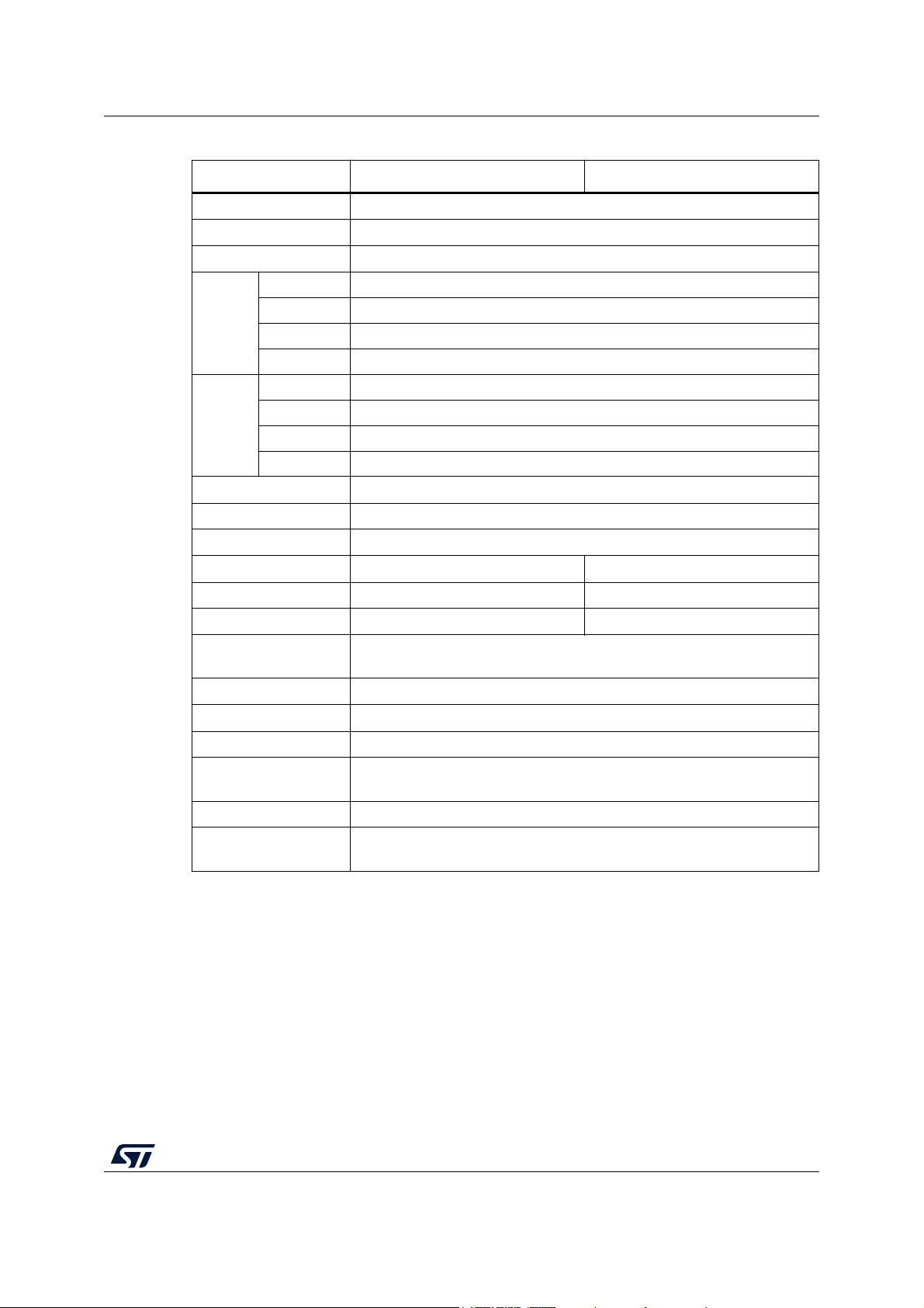
Table 1. STM32WB15CC device features and peripheral counts . . . . . . . . . . . . . . . . . . . . . . . . . . 11
Table 2. Access status vs. readout protection level and execution modes . . . . . . . . . . . . . . . . . . . 15
Table 3. RF pin list . . . . . . . . . . . . . . . . . . . . . . . . . . . . . . . . . . . . . . . . . . . . . . . . . . . . . . . . . . . . . . 19
Table 4. Typical external components . . . . . . . . . . . . . . . . . . . . . . . . . . . . . . . . . . . . . . . . . . . . . . . 20
Table 5. Power supply typical components . . . . . . . . . . . . . . . . . . . . . . . . . . . . . . . . . . . . . . . . . . . 21
Table 6. Functionalities depending on system operating mode . . . . . . . . . . . . . . . . . . . . . . . . . . . . 26
Table 7. STM32WB15CC modes overview . . . . . . . . . . . . . . . . . . . . . . . . . . . . . . . . . . . . . . . . . . . 29
Table 8. STM32WB15CC CPU1 peripherals interconnect matrix. . . . . . . . . . . . . . . . . . . . . . . . . . . 31
Table 9. DMA implementation . . . . . . . . . . . . . . . . . . . . . . . . . . . . . . . . . . . . . . . . . . . . . . . . . . . . . 36
Table 10. Temperature sensor calibration values. . . . . . . . . . . . . . . . . . . . . . . . . . . . . . . . . . . . . . . . 38
Table 11. Internal voltage reference calibration values . . . . . . . . . . . . . . . . . . . . . . . . . . . . . . . . . . . 38
Table 12. Timer features. . . . . . . . . . . . . . . . . . . . . . . . . . . . . . . . . . . . . . . . . . . . . . . . . . . . . . . . . . . 39
Table 13. I2C implementation . . . . . . . . . . . . . . . . . . . . . . . . . . . . . . . . . . . . . . . . . . . . . . . . . . . . . . . 43
Table 14. Legend/abbreviations used in the pinout table . . . . . . . . . . . . . . . . . . . . . . . . . . . . . . . . . . 46
Table 15. STM32WB15CC pin definitions . . . . . . . . . . . . . . . . . . . . . . . . . . . . . . . . . . . . . . . . . . . . . 47
Table 16. Alternate functions . . . . . . . . . . . . . . . . . . . . . . . . . . . . . . . . . . . . . . . . . . . . . . . . . . . . . . . 51
Table 17. Voltage characteristics . . . . . . . . . . . . . . . . . . . . . . . . . . . . . . . . . . . . . . . . . . . . . . . . . . . . 57
Table 18. Current characteristics . . . . . . . . . . . . . . . . . . . . . . . . . . . . . . . . . . . . . . . . . . . . . . . . . . . . 58
Table 19. Thermal characteristics. . . . . . . . . . . . . . . . . . . . . . . . . . . . . . . . . . . . . . . . . . . . . . . . . . . . 58
Table 20. Main performance at VDD = 3.3 V . . . . . . . . . . . . . . . . . . . . . . . . . . . . . . . . . . . . . . . . . . . 59
Table 21. General operating conditions . . . . . . . . . . . . . . . . . . . . . . . . . . . . . . . . . . . . . . . . . . . . . . . 59
Table 22. RF transmitter BLE characteristics . . . . . . . . . . . . . . . . . . . . . . . . . . . . . . . . . . . . . . . . . . . 60
Table 23. RF transmitter BLE characteristics (1 Mbps) . . . . . . . . . . . . . . . . . . . . . . . . . . . . . . . . . . . 61
Table 24. RF transmitter BLE characteristics (2 Mbps) . . . . . . . . . . . . . . . . . . . . . . . . . . . . . . . . . . . 61
Table 25. RF receiver BLE characteristics (1 Mbps) . . . . . . . . . . . . . . . . . . . . . . . . . . . . . . . . . . . . . 62
Table 26. RF receiver BLE characteristics (2 Mbps) . . . . . . . . . . . . . . . . . . . . . . . . . . . . . . . . . . . . . 64
Table 27. RF BLE power consumption for VDD = 3.3 V. . . . . . . . . . . . . . . . . . . . . . . . . . . . . . . . . . . 65
Table 28. Operating conditions at power-up / power-down . . . . . . . . . . . . . . . . . . . . . . . . . . . . . . . . 65
Table 29. Embedded reset and power control block characteristics. . . . . . . . . . . . . . . . . . . . . . . . . . 66
Table 30. Embedded internal voltage reference . . . . . . . . . . . . . . . . . . . . . . . . . . . . . . . . . . . . . . . . . 67
Table 31. Current consumption in Run and Low-power run modes, code with data processing
running from Flash memory, ART enable (Cache ON Prefetch OFF), VDD = 3.3 V . . . . . 69
Table 32. Current consumption in Run and Low-power run modes, code with data processing
running from SRAM1, VDD = 3.3 V . . . . . . . . . . . . . . . . . . . . . . . . . . . . . . . . . . . . . . . . . . 70
Table 33. Typical current consumption in Run and Low-power run modes, with different codes
running from Flash memory, ART enable (Cache ON Prefetch OFF), VDD= 3.3 V . . . . . . 71
Table 34. Typical current consumption in Run and Low-power run modes,
with different codes running from SRAM1, VDD = 3.3 V . . . . . . . . . . . . . . . . . . . . . . . . . . 72
Table 35. Current consumption in Sleep and Low-power sleep modes, Flash memory ON . . . . . . . 73
Table 36. Current consumption in Low-power sleep modes, Flash memory in Power down . . . . . . . 73
Table 37. Current consumption in Stop 1 mode . . . . . . . . . . . . . . . . . . . . . . . . . . . . . . . . . . . . . . . . . 74
Table 38. Current consumption in Stop 0 mode . . . . . . . . . . . . . . . . . . . . . . . . . . . . . . . . . . . . . . . . . 75
Table 39. Current consumption in Standby mode . . . . . . . . . . . . . . . . . . . . . . . . . . . . . . . . . . . . . . . 75
Table 40. Current consumption in Shutdown mode . . . . . . . . . . . . . . . . . . . . . . . . . . . . . . . . . . . . . . 77
Table 41. Current consumption in VBAT mode . . . . . . . . . . . . . . . . . . . . . . . . . . . . . . . . . . . . . . . . . 77
Table 42. Current under Reset condition . . . . . . . . . . . . . . . . . . . . . . . . . . . . . . . . . . . . . . . . . . . . . . 78
Table 43. Peripheral current consumption . . . . . . . . . . . . . . . . . . . . . . . . . . . . . . . . . . . . . . . . . . . . . 80
Table 44. Low-power mode wakeup timings . . . . . . . . . . . . . . . . . . . . . . . . . . . . . . . . . . . . . . . . . . . 82
6/121 DS13258 Rev 1

STM32WB15CC List of tables
Table 45. Regulator modes transition times . . . . . . . . . . . . . . . . . . . . . . . . . . . . . . . . . . . . . . . . . . . . 82
Table 46. Wakeup time using LPUART . . . . . . . . . . . . . . . . . . . . . . . . . . . . . . . . . . . . . . . . . . . . . . . 83
Table 47. HSE crystal requirements . . . . . . . . . . . . . . . . . . . . . . . . . . . . . . . . . . . . . . . . . . . . . . . . . . 83
Table 48. HSE clock source requirements . . . . . . . . . . . . . . . . . . . . . . . . . . . . . . . . . . . . . . . . . . . . . 83
Table 49. HSE oscillator characteristics . . . . . . . . . . . . . . . . . . . . . . . . . . . . . . . . . . . . . . . . . . . . . . . 84
Table 50. Low-speed external user clock characteristics . . . . . . . . . . . . . . . . . . . . . . . . . . . . . . . . . . 84
Table 51. Low-speed external user clock characteristics – Bypass mode . . . . . . . . . . . . . . . . . . . . . 86
Table 52. HSI16 oscillator characteristics. . . . . . . . . . . . . . . . . . . . . . . . . . . . . . . . . . . . . . . . . . . . . . 86
Table 53. MSI oscillator characteristics
. . . . . . . . . . . . . . . . . . . . . . . . . . . . . . . . . . . . . . . . . . . . . . . . . . . . .88
Table 54. LSI1 oscillator characteristics . . . . . . . . . . . . . . . . . . . . . . . . . . . . . . . . . . . . . . . . . . . . . . . 91
Table 55. LSI2 oscillator characteristics . . . . . . . . . . . . . . . . . . . . . . . . . . . . . . . . . . . . . . . . . . . . . . . 91
Table 56. PLL characteristics . . . . . . . . . . . . . . . . . . . . . . . . . . . . . . . . . . . . . . . . . . . . . . . . . . . . . . . 91
Table 57. Flash memory characteristics . . . . . . . . . . . . . . . . . . . . . . . . . . . . . . . . . . . . . . . . . . . . . . . 92
Table 58. Flash memory endurance and data retention . . . . . . . . . . . . . . . . . . . . . . . . . . . . . . . . . . . 92
Table 59. EMS characteristics . . . . . . . . . . . . . . . . . . . . . . . . . . . . . . . . . . . . . . . . . . . . . . . . . . . . . . 93
Table 60. EMI characteristics . . . . . . . . . . . . . . . . . . . . . . . . . . . . . . . . . . . . . . . . . . . . . . . . . . . . . . . 94
Table 61. ESD absolute maximum ratings . . . . . . . . . . . . . . . . . . . . . . . . . . . . . . . . . . . . . . . . . . . . . 94
Table 62. Electrical sensitivity. . . . . . . . . . . . . . . . . . . . . . . . . . . . . . . . . . . . . . . . . . . . . . . . . . . . . . . 95
Table 63. I/O current injection susceptibility . . . . . . . . . . . . . . . . . . . . . . . . . . . . . . . . . . . . . . . . . . . . 95
Table 64. I/O static characteristics . . . . . . . . . . . . . . . . . . . . . . . . . . . . . . . . . . . . . . . . . . . . . . . . . . . 96
Table 65. Output voltage characteristics . . . . . . . . . . . . . . . . . . . . . . . . . . . . . . . . . . . . . . . . . . . . . . 98
Table 66. I/O AC characteristics . . . . . . . . . . . . . . . . . . . . . . . . . . . . . . . . . . . . . . . . . . . . . . . . . . . . . 98
Table 67. NRST pin characteristics . . . . . . . . . . . . . . . . . . . . . . . . . . . . . . . . . . . . . . . . . . . . . . . . . 100
Table 68. Analog switches booster characteristics . . . . . . . . . . . . . . . . . . . . . . . . . . . . . . . . . . . . . . 101
Table 69. ADC characteristics . . . . . . . . . . . . . . . . . . . . . . . . . . . . . . . . . . . . . . . . . . . . . . . . . . . . . 101
Table 70. Maximum ADC R
values . . . . . . . . . . . . . . . . . . . . . . . . . . . . . . . . . . . . . . . . . . . . . . . 103
AIN
Table 71. ADC accuracy . . . . . . . . . . . . . . . . . . . . . . . . . . . . . . . . . . . . . . . . . . . . . . . . . . . . . . . . . . 104
Table 72. COMP characteristics . . . . . . . . . . . . . . . . . . . . . . . . . . . . . . . . . . . . . . . . . . . . . . . . . . . . 106
Table 73. TS characteristics . . . . . . . . . . . . . . . . . . . . . . . . . . . . . . . . . . . . . . . . . . . . . . . . . . . . . . . 107
Table 74. V
Table 75. V
monitoring characteristics . . . . . . . . . . . . . . . . . . . . . . . . . . . . . . . . . . . . . . . . . . . . 108
BAT
charging characteristics . . . . . . . . . . . . . . . . . . . . . . . . . . . . . . . . . . . . . . . . . . . . . . 108
BAT
Table 76. TIMx characteristics . . . . . . . . . . . . . . . . . . . . . . . . . . . . . . . . . . . . . . . . . . . . . . . . . . . . . 108
Table 77. IWDG min/max timeout period at 32 kHz (LSI1). . . . . . . . . . . . . . . . . . . . . . . . . . . . . . . . 109
Table 78. Minimum I2CCLK frequency in all I2C modes . . . . . . . . . . . . . . . . . . . . . . . . . . . . . . . . . 109
Table 79. I2C analog filter characteristics. . . . . . . . . . . . . . . . . . . . . . . . . . . . . . . . . . . . . . . . . . . . . 110
Table 80. SPI characteristics . . . . . . . . . . . . . . . . . . . . . . . . . . . . . . . . . . . . . . . . . . . . . . . . . . . . . . 110
Table 81. JTAG characteristics. . . . . . . . . . . . . . . . . . . . . . . . . . . . . . . . . . . . . . . . . . . . . . . . . . . . . 113
Table 82. SWD characteristics . . . . . . . . . . . . . . . . . . . . . . . . . . . . . . . . . . . . . . . . . . . . . . . . . . . . . 113
Table 83. UFQFPN48 mechanical data . . . . . . . . . . . . . . . . . . . . . . . . . . . . . . . . . . . . . . . . . . . . . . 115
Table 84. Package thermal characteristics . . . . . . . . . . . . . . . . . . . . . . . . . . . . . . . . . . . . . . . . . . . . 117
Table 85. Document revision history . . . . . . . . . . . . . . . . . . . . . . . . . . . . . . . . . . . . . . . . . . . . . . . . 120
DS13258 Rev 1 7/121
7

List of figures STM32WB15CC
List of figures
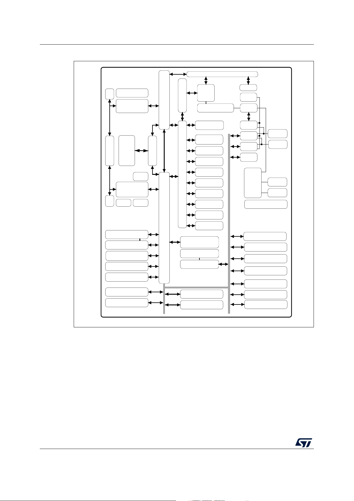
Figure 1. STM32WB15CC block diagram . . . . . . . . . . . . . . . . . . . . . . . . . . . . . . . . . . . . . . . . . . . . . 12
Figure 2. STM32WB15CC RF front-end block diagram. . . . . . . . . . . . . . . . . . . . . . . . . . . . . . . . . . . 18
Figure 3. External components for the RF part . . . . . . . . . . . . . . . . . . . . . . . . . . . . . . . . . . . . . . . . . 20
Figure 4. Power distribution . . . . . . . . . . . . . . . . . . . . . . . . . . . . . . . . . . . . . . . . . . . . . . . . . . . . . . . . 21
Figure 5. Power-up/down sequence . . . . . . . . . . . . . . . . . . . . . . . . . . . . . . . . . . . . . . . . . . . . . . . . . 22
Figure 6. Power supply overview . . . . . . . . . . . . . . . . . . . . . . . . . . . . . . . . . . . . . . . . . . . . . . . . . . . . 23
Figure 7. Clock tree . . . . . . . . . . . . . . . . . . . . . . . . . . . . . . . . . . . . . . . . . . . . . . . . . . . . . . . . . . . . . . 35
Figure 8. STM32WB15CCU UFQFPN48 pinout
Figure 9. STM32WB15CCU UFQFPN48E pinout
Figure 10. Pin loading conditions . . . . . . . . . . . . . . . . . . . . . . . . . . . . . . . . . . . . . . . . . . . . . . . . . . . . . 55
Figure 11. Pin input voltage . . . . . . . . . . . . . . . . . . . . . . . . . . . . . . . . . . . . . . . . . . . . . . . . . . . . . . . . . 55
Figure 12. Power supply scheme. . . . . . . . . . . . . . . . . . . . . . . . . . . . . . . . . . . . . . . . . . . . . . . . . . . . . 56
Figure 13. Current consumption measurement scheme . . . . . . . . . . . . . . . . . . . . . . . . . . . . . . . . . . . 57
Figure 14. VREFINT vs. temperature . . . . . . . . . . . . . . . . . . . . . . . . . . . . . . . . . . . . . . . . . . . . . . . . . 68
Figure 15. Typical application with a 32.768 kHz crystal . . . . . . . . . . . . . . . . . . . . . . . . . . . . . . . . . . . 85
Figure 16. Low-speed external clock source AC timing diagram. . . . . . . . . . . . . . . . . . . . . . . . . . . . . 86
Figure 17. HSI16 frequency vs. temperature . . . . . . . . . . . . . . . . . . . . . . . . . . . . . . . . . . . . . . . . . . . . 87
Figure 18. Typical current consumption vs. MSI frequency . . . . . . . . . . . . . . . . . . . . . . . . . . . . . . . . . 90
Figure 19. I/O input characteristics . . . . . . . . . . . . . . . . . . . . . . . . . . . . . . . . . . . . . . . . . . . . . . . . . . . 97
Figure 20. Recommended NRST pin protection . . . . . . . . . . . . . . . . . . . . . . . . . . . . . . . . . . . . . . . . 100
Figure 21. ADC accuracy characteristics . . . . . . . . . . . . . . . . . . . . . . . . . . . . . . . . . . . . . . . . . . . . . . 105
Figure 22. Typical connection diagram using the ADC . . . . . . . . . . . . . . . . . . . . . . . . . . . . . . . . . . . 106
Figure 23. SPI timing diagram - Slave mode and CPHA = 0 . . . . . . . . . . . . . . . . . . . . . . . . . . . . . . . 111
Figure 24. SPI timing diagram - Slave mode and CPHA = 1 . . . . . . . . . . . . . . . . . . . . . . . . . . . . . . . 112
Figure 25. SPI timing diagram - Master mode . . . . . . . . . . . . . . . . . . . . . . . . . . . . . . . . . . . . . . . . . . 112
Figure 26. UFQFPN48 outline . . . . . . . . . . . . . . . . . . . . . . . . . . . . . . . . . . . . . . . . . . . . . . . . . . . . . . 114
Figure 27. UFQFPN48 recommended footprint . . . . . . . . . . . . . . . . . . . . . . . . . . . . . . . . . . . . . . . . . 115
Figure 28. UFQFPN48 marking example (package top view) . . . . . . . . . . . . . . . . . . . . . . . . . . . . . . 116
(1) (2)
. . . . . . . . . . . . . . . . . . . . . . . . . . . . . . . . . . . . 45
(1) (2)
. . . . . . . . . . . . . . . . . . . . . . . . . . . . . . . . . . . 45
8/121 DS13258 Rev 1
STM32WB15CC Introduction
1 Introduction
This document provides the ordering information and mechanical device characteristics of
the STM32WB15CC microcontroller, based on Arm
®
cores
(a)
. Throughout the whole
document TBD indicates a value to be defined.
This document must be read in conjunction with the reference manual (RM0473), available
from the STMicroelectronics website www.st.com.
For information on the Arm® Cortex®-M4 and Cortex®-M0+ cores, refer, respectively, to the
®
Cortex
-M4 Technical Reference Manual and to the Cortex®-M0+ Technical Reference
Manual, both available on the www.arm.com website.
For information on Bluetooth® refer to www.bluetooth.com.
a. Arm is a registered trademark of Arm Limited (or its subsidiaries) in the US and/or elsewhere.
DS13258 Rev 1 9/121
44

Description STM32WB15CC
2 Description
The STM32WB15CC multiprotocol wireless and ultra-low-power device embeds a powerful
and ultra-low-power radio compliant with the Bluetooth
It contains a dedicated Arm
®
Cortex® -M0+ for performing all the real-time low layer
®
Low Energy SIG specification v5.2.
operation.
The device is designed to be extremely low-power and is based on the high-performance
®
Arm
Cortex®-M4 32-bit RISC core operating at a frequency of up to 64 MHz. This core
features a Floating point unit (FPU) single precision that supports all Arm
®
single-precision data-processing instructions and data types. It also implements a full set of
DSP instructions and a memory protection unit (MPU) that enhances application security.
Enhanced inter-processor communication is provided by the IPCC with six bidirectional
channels. The HSEM provides hardware semaphores used to share common resources
between the two processors.
The device embeds high-speed memories (320 Kbyte of Flash memory, 48 Kbytes of
SRAM) and an extensive range of enhanced I/Os and peripherals.
Direct data transfer between memory and peripherals and from memory to memory is
supported by seven DMA channels with a full flexible channel mapping by the DMAMUX
peripheral.
The device feature several mechanisms for embedded Flash memory and SRAM: readout
protection, write protection and proprietary code readout protection. Portions of the memory
can be secured for Cortex
®
-M0+ exclusive access.
The AES encryption engine, PKA and RNG enable upper layer cryptography.
The device offers a fast 12-bit ADC and one ultra-low-power comparator.
The device embeds a low-power RTC, one advanced 16-bit timer, one general-purpose
32-bit timer, and two 16-bit low-power timers.
In addition, up to eight capacitive sensing channels are available.
The STM32WB15CC also features standard and advanced communication interfaces,
namely one USART (ISO 7816, IrDA, Modbus and Smartcard mode), one
low- power UART (LPUART), one I2C (SMBus/PMBus), one SPI up to 32 MHz.
The STM32WB15CC operates in the -40 to +85 °C (+105 °C junction) and -40 to +105 °C
(+125
°C junction) temperature ranges from a 1.71 to 3.6 V power supply. A comprehensive
set of power-saving modes enables the design of low-power applications.
The STM32WB15CC integrates a high efficiency SMPS step-down converter with automatic
bypass mode capability when the V
is 2.0
V). It includes independent power supplies for analog input for ADC and comparator.
A V
dedicated supply allows the device to back up the LSE 32.768 kHz oscillator, the
BAT
falls below V
DD
(x=1, 2, 3, 4) voltage level (default
BORx
RTC and the backup registers, thus enabling the STM32WB15CC to supply these functions
even if the main V
is not present through a CR2032-like battery, a Supercap or a small
DD
rechargeable battery.
The STM32WB15CC offers one package, 48 pins.
10/121 DS13258 Rev 1
STM32WB15CC Description
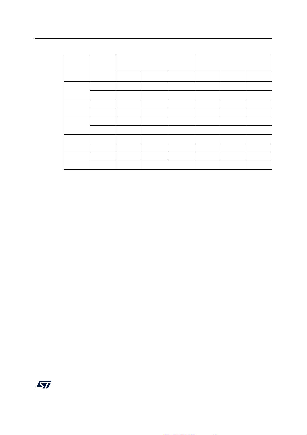
Table 1. STM32WB15CC device features and peripheral counts
Feature STM32WB15CCUxE STM32WB15CCU
Flash memory density 320 KB
SRAM density 48 KB
BLE V5.2 (2 Mbps)
Advanced 1 (16 bits)
Timers
Comm
interface
RTC 1
Tamper pin 1
Wakeup pin 2
General 1 (32 bits)
Low power 2 (16 bits)
SysTick 1
SPI 1
I2C 1
USART
(1)
1
LPUART 1
GPIOs 37 30
Capacitive sensing 8 3
SMPS No Yes
12-bit ADC
Number of channels
Internal V
ref
13 channels
(including 3 internal)
Yes
Analog comparator 1
Max CPU frequency 64 MHz
Operating temperature
Ambient operating temperature:-40 to +85 °C and -40 to +105 °C
Junction temperature: -40 to +105 °C and -40 to +125 °C
Operating voltage 1.71 to 3.6 V
Package
1. USART peripheral can be used as SPI master.
UFQFPN48 7 x 7 mm
0.5 mm pitch, solder pad
DS13258 Rev 1 11/121
44
Description STM32WB15CC
MS53541V3
NVIC
TIM2
PWR
TIM1
GPIO ports
A, B, C, E, H
EXTI
12 KB SRAM1
RTC2
I-WDG
LSE
32 kHz
HSE2
32 MHz
MSI up to
48 MHz
HSI 1%
16 MHz
PLL1
Power supply POR/
PDR/BOR/PVD/AVD
ADC1 12-bit ULP
2.5 Msps / 13 ch
NVIC
JTAG/SWD
AHB Lite
IPCC
Arbiter + ART
320 KB Flash
shared memory
BLE IP
RNG
LSI1
32 kHz
BLE RF IP
LPTIM2
LPTIM1
AES2
DBG
AHB lite (shared)
WKUP
BLE
AHB asynchronous
CRC
RCC + CSS
SYSCFG/COMP
APB asynchronous
RCC2
TSC
HSEM
WWDG
LPUART1
SPI1
I2C1
USART1
PKA + RAM
LSI2
32 kHz
MPU
Cortex-M0+
32 KB SRAM2a
Cortex-M4
(DSP)
4 KB SRAM2b
FPU
CTI CTI
TAMP
DMAMUX
AHB Lite
Temp (
o
C) sensor
DMA1 - 7 channels
APB
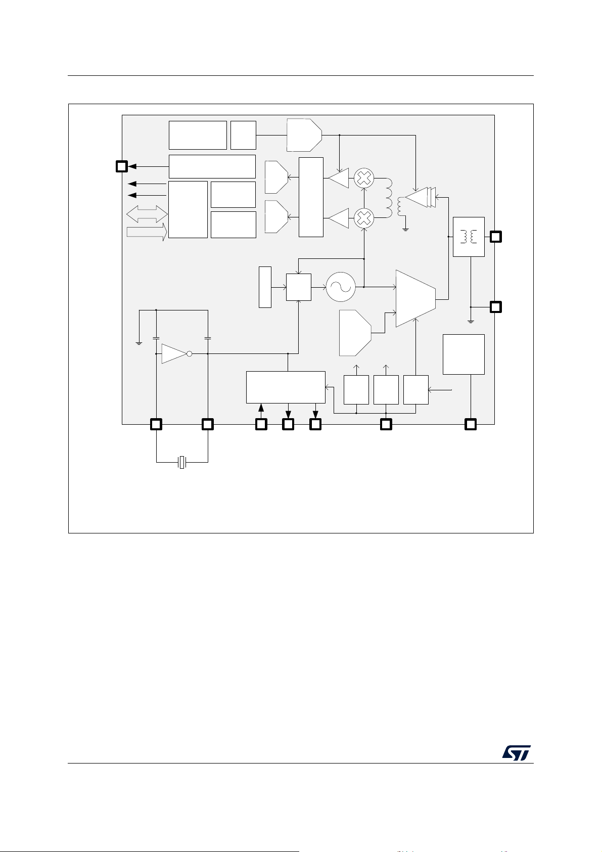
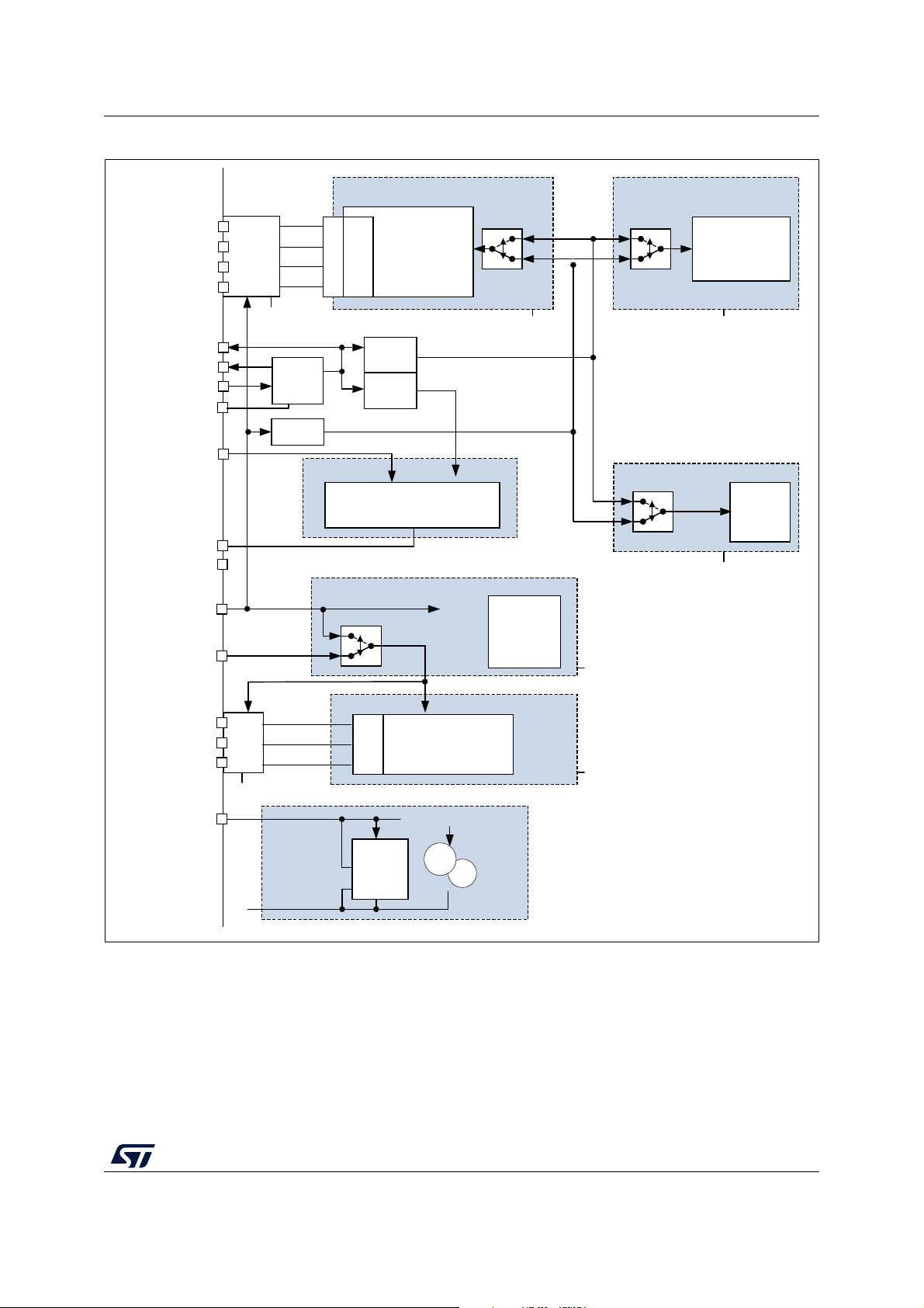
Figure 1. STM32WB15CC block diagram
12/121 DS13258 Rev 1

STM32WB15CC Functional overview
3 Functional overview
3.1 Architecture
The STM32WB15CC multiprotocol wireless device embeds a BLE RF subsystem that
interfaces with a generic microcontroller subsystem using an Arm
CPU1) on which the host application resides.
The RF subsystem is composed of an RF analog front end, BLE block as well as of a
dedicated Arm
The RF subsystem performs all of the BLE stack, reducing the interaction with the CPU1 to
high level exchanges.
Some functions are shared between the RF subsystem CPU (CPU2) and the Host CPU
(CPU1):
Flash memories
SRAM1, SRAM2a and SRAM2b (all can be retained in Standby mode)
Security peripherals (RNG, PKA)
Clock RCC
Power control (PWR)
The communication and the sharing of peripherals between the RF subsystem and the
®
Cortex
controller (IPCC) and semaphore mechanism (HSEM).
®
Cortex®-M0+ microcontroller (called CPU2), plus proprietary peripherals.
-M4 CPU is performed through a dedicated inter processor communication
3.2 Arm® Cortex®-M4 core with FPU
The Arm® Cortex®-M4 with FPU is a processor for embedded systems. It has been
developed to provide a low-cost platform that meets the needs of MCU implementation, with
a reduced pin count and low-power consumption, while delivering outstanding
computational performance and an advanced response to interrupts.
®
Cortex®-M4 CPU (called
The Arm® Cortex®-M4 with FPU 32-bit RISC processor features exceptional
code-efficiency, delivering the high-performance expected from an Arm® core in the
memory size usually associated with 8- and 16-bit devices.
The processor supports a set of DSP instructions enabling efficient signal processing and
complex algorithm execution.
Its single precision FPU speeds up software development by using metalanguage
development tools, while avoiding saturation.
With its embedded Arm® core, the STM32WB15CC is compatible with all Arm® tools and
software.
Figure 1 shows the general block diagram of the device.
DS13258 Rev 1 13/121
44

Functional overview STM32WB15CC
3.3 Memories
3.3.1 Adaptive real-time memory accelerator (ART Accelerator)
The ART Accelerator is a memory accelerator optimized for STM32 industry-standard Arm®
®
Cortex
Cortex
for the Flash memory at higher frequencies.
To release the processor near 80 DMIPS performance at 64 MHz, the accelerator
implements an instruction prefetch queue and branch cache, which increases program
execution speed from the 64-bit Flash memory. Based on CoreMark benchmark, the
performance achieved thanks to the ART accelerator is equivalent to 0 wait state program
execution from Flash memory at a CPU frequency up to 64 MHz.
3.3.2 Memory protection unit
The memory protection unit (MPU) is used to manage the CPU1 accesses to memory to
prevent one task to accidentally corrupt the memory or resources used by any other active
task. This memory area is organized into up to eight protected areas, which can be divided
up into eight subareas. The protection area sizes are between 32 bytes and the whole
4
-M4 processors. It balances the inherent performance advantage of the Arm®
®
-M4 over Flash memory technologies, which normally require the processor to wait
Gbytes of addressable memory.
The MPU is especially helpful for applications where some critical or certified code must be
protected against the misbehavior of other tasks. It is usually managed by an RTOS
(real-time operating system). If a program accesses a memory location prohibited by the
MPU, the RTOS detects it and takes action. In an RTOS environment, the kernel can
dynamically update the MPU area setting, based on the process to be executed.
The MPU is optional and can be bypassed for applications that do not need it.
3.3.3 Embedded Flash memory
The STM32WB15CC device features 320 Kbytes of embedded Flash memory available for
storing programs and data, as well as some customer keys.
Flexible protections can be configured thanks to option bytes:
Readout protection (RDP) to protect the whole memory. Three levels are available:
– Level 0: no readout protection
– Level 1: memory readout protection: the Flash memory cannot be read from or
written to if either debug features are connected, boot in SRAM or bootloader is
selected
– Level 2: chip readout protection: debug features (Cortex
JTAG and serial wire), boot in SRAM and bootloader selection are disabled (JTAG
fuse). This selection is irreversible.
®
-M4 and Cortex®-M0+
14/121 DS13258 Rev 1
STM32WB15CC Functional overview
Table 2. Access status vs. readout protection level and execution modes
Area
Main
memory
System
memory
Option
bytes
Backup
registers
SRAM2a
SRAM2b
1. The option byte can be modified by the RF subsystem.
2. Erased when RDP changes from Level 1 to Level 0.
Protection
level
1 Yes Yes Yes No No No
2 Yes Yes Yes N/A N/A N/A
1 Yes No No Yes No No
2 Yes No No N/A N/A N/A
1 Yes Yes Yes Yes Yes Yes
2YesNo
1YesYesN/A
2 Yes Yes N/A N/A N/A N/A
1 Yes Yes Yes
2 Yes Yes Yes N/A N/A N/A
User execution
Read Write Erase Read Write Erase
(1)
No
(1)
Debug, boot from SRAM or boot
from system memory (loader)
N/A N/A N/A
(2)
(2)
No No N/A
No No No
(2)
(2)
Write protection (WRP): the protected area is protected against erasing and
programming. Two areas can be selected, with 4-Kbyte granularity.
Proprietary code readout protection (PCROP): two parts of the Flash memory can be
protected against read and write from third parties. The protected area is execute-only:
it can only be reached by the STM32 CPU, as an instruction code, while all other
accesses (DMA, debug and CPU data read, write and erase) are strictly prohibited.
Two areas can be selected, with 2-Kbyte granularity. An additional option bit
(PCROP_RDP) makes possible to select if the PCROP area is erased or not when the
RDP protection is changed from Level 1 to Level 0.
A section of the Flash memory is secured for the RF subsystem CPU2, and cannot be
accessed by the host CPU1.
The whole non-volatile memory embeds the error correction code (ECC) feature supporting:
single error detection and correction
double error detection
the address of the ECC fail can be read in the ECC register
The embedded Flash memory is shared between CPU1 and CPU2 on a time sharing basis.
A dedicated HW mechanism allows both CPUs to perform Write/Erase operations.
3.3.4 Embedded SRAM
The STM32WB15CC device features 48 Kbytes of embedded SRAM, split in three blocks:
SRAM1: 12 Kbytes mapped at address 0x2000 0000
SRAM2a: 32 Kbytes located at address 0x2003 0000 also mirrored at 0x1000 0000,
with hardware parity check
SRAM2b: 4 Kbytes located at address 0x2003 8000 (contiguous with SRAM2a) and
mirrored at 0x1000 8000 with hardware parity check
DS13258 Rev 1 15/121
44

Functional overview STM32WB15CC
SRAM2a and SRAM2b can be write-protected, with 1-Kbyte granularity. A section of the
SRAM2a and SRAM2b is secured for the RF sub-system and cannot be accessed by the
host CPU1.
The SRAMs can be accessed in read/write with 0 wait states for all CPU1 and CPU2 clock
speeds.
3.4 Security and safety
The STM32WB15CC contains many security blocks both for the BLE and the Host
application.
It includes:
Secure Flash memory partition for RF subsystem-only access
Secure SRAM partition, that can be accessed only by the RF subsystem
True random number generator (RNG)
Advance encryption standard hardware accelerator (AES-256bit, supporting chaining
modes ECB, CBC, CTR, GCM, GMAC, CCM)
Private key acceleration (PKA) including:
– Modular arithmetic including exponentiation with maximum modulo size of 3136
bits
– Elliptic curves over prime field scalar multiplication, ECDSA signature, ECDSA
verification with maximum modulo size of 521 bits
Cyclic redundancy check calculation unit (CRC)
A specific mechanism is in place to ensure that all the code executed by the RF subsystem
CPU2 can be secure, whatever the Host application.
3.5 Boot modes and FW update
At startup, BOOT0 pin and BOOT1 option bit are used to select one of three boot options:
Boot from user Flash
Boot from system memory
Boot from embedded SRAM
The device always boots on CPU1 core. The embedded bootloader code makes it possible
to boot from various peripherals:
UART
I2C
SPI
Secure Firmware update from system boot is provided.
3.6 RF subsystem
The STM32WB15CC embed an ultra-low power multi-standard radio Bluetooth® Low
Energy (BLE), compliant with Bluetooth
2
Mbps transfer rates, supports multiple roles simultaneously acting at the same time as
®
specification v5.2. The BLE features 1 Mbps and
16/121 DS13258 Rev 1

STM32WB15CC Functional overview
BLE sensor and hub device, embeds Elliptic Curve Diffie-Hellman (ECDH) key agreement
protocol, thus ensuring a secure connection.
The BLE stack runs on an embedded Arm® Cortex®-M0+ core (CPU2). The stack is stored
on the embedded Flash memory, which is also shared with the Arm
application, making it possible in-field stack update.
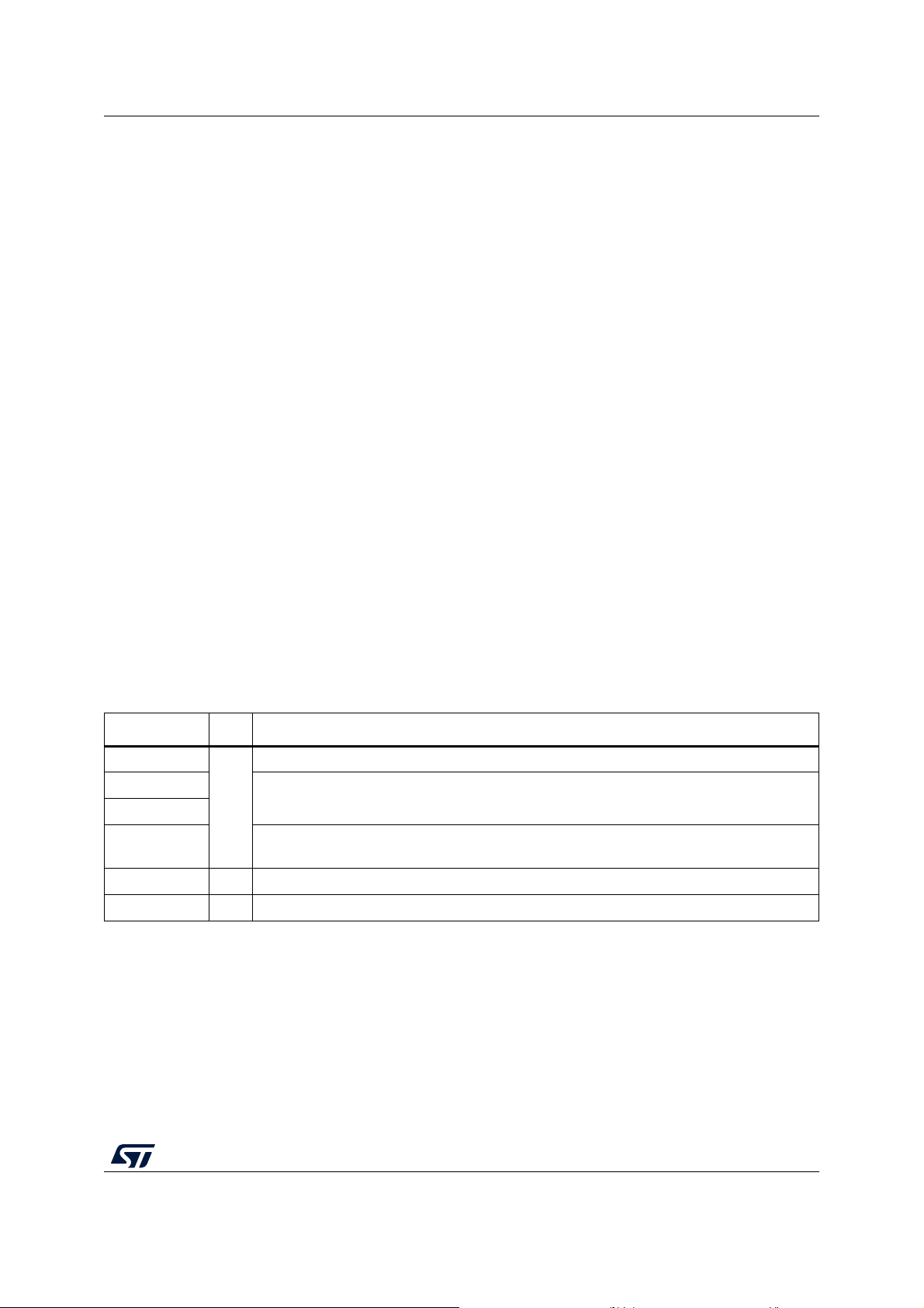
3.6.1 RF front-end block diagram
The RF front-end is based on a direct modulation of the carrier in Tx, and uses a low IF
architecture in Rx mode.
Thanks to an internal transformer at RF pins, the circuit directly interfaces the antenna
(single ended connection, impedance close to 50 ). The natural bandpass behavior of the
internal transformer, simplifies outside circuitry aimed for harmonic filtering and out of band
interferer rejection.
In Transmit mode, the maximum output power is user selectable through the programmable
LDO voltage of the power amplifier. A linearized, smoothed analog control offers clean
power ramp-up.
In receive mode the circuit can be used in standard high performance or in reduced power
consumption (user programmable). The Automatic gain control (AGC) is able to reduce the
chain gain at both RF and IF locations, for optimized interference rejection. Thanks to the
use of complex filtering and highly accurate I/Q architecture, high sensitivity and excellent
linearity can be achieved.
The bill of material is reduced thanks to the high degree of integration. The radio frequency
source is synthesized form an external 32 MHz crystal that does not need any external
trimming capacitor network thanks to a dual network of user programmable integrated
capacitors.
®
Cortex®-M4 (CPU1)
DS13258 Rev 1 17/121
44
Functional overview STM32WB15CC
MS53542V2
Note: UFQFPN48: V
SS
through exposed pad, and V
SSRF
pin must be connected to ground plane
PA
BP
filter
ADC
ADC
PLL
Modulator
RF1
Adjust
32 MHz
OSC_OUTOSC_IN
PA ramp
generator
AGC
control
BLE
modulator
BLE
demodulator
BLE
controller
RF control
AGC
Timer and Power
control
LDO LDO LDO
V
FBSMPS
Trimmed
bias
V
DDRF
Max PA
level
SMPS
V
LXSMPS
V
DDSMPSVSSSMPS
Adjust
HSE
G
G
LNA
Wakeup
Interrupt
AHB
APB
See
note
RF_TX_
MOD_
EXT_PA
Figure 2. STM32WB15CC RF front-end block diagram
3.6.2 BLE general description
The BLE block is a master/slave processor, compliant with Bluetooth specification 5.2
standard (2
It integrates a 2.4 GHz RF transceiver and a powerful Cortex®-M0+ core, on which a
Mbps).
complete power-optimized stack for Bluetooth Low Energy protocol runs, providing
master
/ slave role support
GAP: central, peripheral, observer or broadcaster roles
ATT/GATT: client and server
SM: privacy, authentication and authorization
L2CAP
Link layer: AES-128 encryption and decryption
18/121 DS13258 Rev 1
STM32WB15CC Functional overview
In addition, according to Bluetooth specification v5.2, the BLE block provides:
Multiple roles simultaneous support
Master/slave and multiple roles simultaneously
LE data packet length extension (making it possible to reach 800 kbps at application
level)
LE privacy 1.2
LE secure connections
Flexible Internet connectivity options
High data rate (2 Mbps)
The device allows the applications to meet the tight peak current requirements imposed by
the use of standard coin cell batteries. When the high efficiency embedded SMPS
step-down converter is used, the RF front end consumption (I
) is only TBD mA at the
tmax
highest output power (TBD dBm).
Ultra-low-power sleep modes and very short transition time between operating modes result
in very low average current consumption during real operating conditions, resulting in longer
battery life.
The BLE block integrates a full bandpass balun, thus reducing the need for external
components.
The link between the Cortex®-M4 application processor (CPU1) running the application, and
the BLE stack running on the dedicated Cortex
®
-M0+ (CPU2) is performed through a
normalized API, using a dedicated IPCC.
3.6.3 RF pin description
The RF block contains dedicated pins, listed in Table 3.
:
Name Type Description
RF1
OSC_OUT
OSC_IN
RF_TX_
MOD_EXT_PA
VDDRF V
VSSRF
1. On packages with exposed pad, this pad must be connected to GND plane for correct RF operation.
(1)
RF Input/output, must be connected to the antenna through a low-pass matching network
32 MHz main oscillator, also used as HSE source
I/O
External PA transmit control
Dedicated supply, must be connected to V
DD
VSSTo be connected to GND
Table 3. RF pin list
DD
3.6.4 Typical RF application schematic
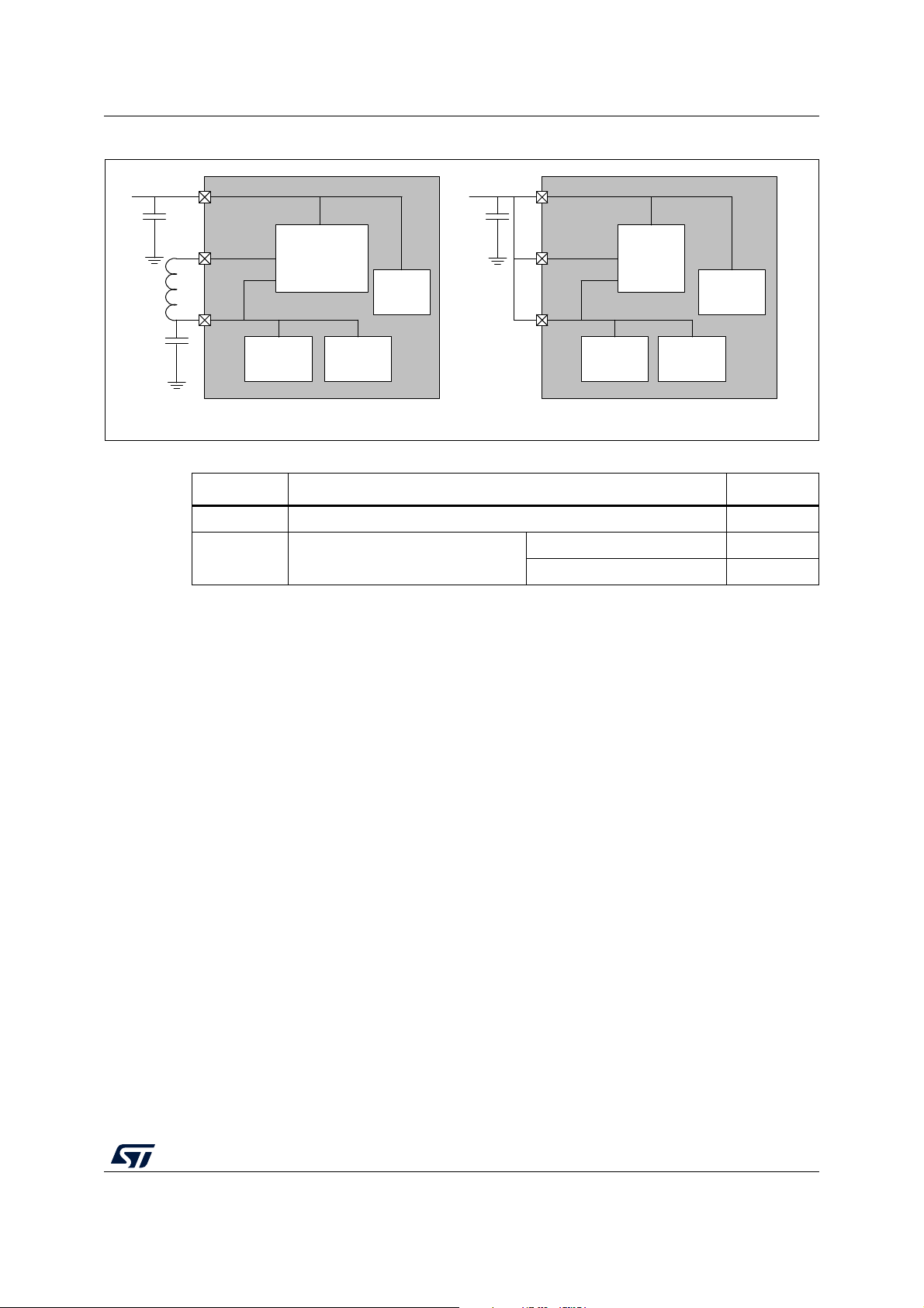
The schematic in Figure 3 and the external components listed in Table 3 are purely
indicative. For more details refer to the “Reference design” provided in separate documents.
DS13258 Rev 1 19/121
44
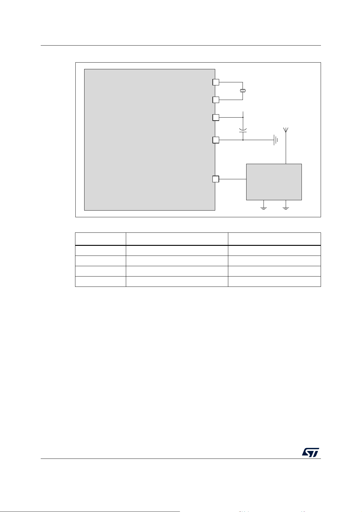
Functional overview STM32WB15CC
MS53575V1
STM32WB
microcontroller
V
DD
OSC_IN
OSC_OUT
VDDRF
VSSRF
RF1
Antenna
Cf1 Cf2
Lf1
Lf2
X1
C1
Antenna filter
(including exposed pad)
32 MHz
Figure 3. External components for the RF part
Component Description Value
C1 Decoupling capacitance for RF 100 nF // 100 pF
X1 32 MHz crystal
Antenna filter Antenna filter and matching network Refer to AN5165, on www.st.com
Antenna 2.4 GHz band antenna -
1. e.g. NDK reference: NX2016SA 32 MHz EXS00A-CS06654.
Table 4. Typical external components
(1)
32 MHz
Note: For more details refer to AN5165 “Development of RF hardware using STM32WB
microcontrollers” available on www.st.com.
3.7 Power supply management
3.7.1 Power supply distribution
The device integrate an SMPS step-down converter to improve low power performance
when the V
automatically enters in bypass mode when the V
(x = 1, 2, 3 or 4) voltage.
By default, at Reset the SMPS is in bypass mode.
The device can be operated without the SMPS by just wiring its output to VDD. This is the
case for applications where the voltage is low, or where the power consumption is not
critical.
voltage is high enough. This converter has an intelligent mode that
DD
voltage falls below a specific BORx
DD
20/121 DS13258 Rev 1
STM32WB15CC Functional overview
MS41409V4
MR
LPR
RFR
SMPS
(not used)
MR
LPR
RFR
V
DD
L1
C2
SMPS configuration LDO configuration
V
DD
VDDSMPS
VLXSMPS
VFBSMPS
SMPS
SMPS mode or
BYPASS mode
VDDSMPS
VLXSMPS
VFBSMPS
Figure 4. Power distribution
Table 5. Power supply typical components
Component Description Value
C2 SMPS output capacitor
(2)
L1
1. e.g. GRM155R60J475KE19.
2. An extra 10 nH inductor in series with L1 is needed to improve the receiver performance,
e.g Murata LQG15WZ10NJ02D
3. e.g. Wurth 74479774222.
4. e.g. Murata LQM21FN100M70L.
SMPS inductance
(1)
For 8 MHz
For 4 MHz
(3)
(4)
4.7 µF
2.2 µH
10 µH
The SMPS can also be switched on or set in bypass mode at any time by the application
software, for example when very accurate ADC measurement are needed.
3.7.2 Power supply schemes
The device has different voltage supplies (see Figure 6) and can operate within the following
voltage ranges:
V
V
During power up/down, the following power sequence requirements must be respected:
When VDD is below 1 V the other power supply (V
When V
= 1.71 to 3.6 V: external power supply for I/Os (V
DD
), the internal regulator and
DDIO
system functions such as RF, SMPS, reset, power management and internal clocks. It
is provided externally through VDD pins. V
DDRF
and V
DDSMPS
must be always
connected to VDD pins.
= 1.62 (ADC/COMPs) to 3.6 V: external analog power supply for ADC and
DDA
comparator. The V
not used V
V
+ 300 mV
DD
must be connected to VDD.
DDA
is above 1 V all power supplies are independent.
DD
voltage level can be independent from the VDD voltage. When
DDA
), must remain below
DDA
DS13258 Rev 1 21/121
44
Functional overview STM32WB15CC
MSv47490V1
0.3
1
V
BOR0
3.6
Operating modePower-on Power-down time
V
V
DDX
(1)
V
DD
Invalid supply area V
DDX
< V
DD
+ 300 mV
V
DDX
independent from V
DD
Figure 5. Power-up/down sequence
1. V
DDX
During the power down phase, VDD can temporarily become lower than other supplies only
if the energy provided to the MCU remains below 1 mJ. This allows the external decoupling
capacitors to be discharged with different time constants during the power down transient
phase.
Note: VDD, V
sequence.
refers to V
and V
DDRF
.
DDA
DDSMPS
must be wired together, so they can follow the same voltage
22/121 DS13258 Rev 1
STM32WB15CC Functional overview
MS53544V2
VBAT
IOs
Wakeup domain (V
DDIO
)
Analog domain
Interruptible domain (V
DD12I
)
Switch domain (V
SW
)
(CPU1, CPU2,
peripherals)
Level shifter
Power switch
V
BAT
ADC
V
DDA
V
REF-
V
DD
HSI, HSE,
PLL, LSI1,
LSI2, IWDG,
RF
IOs
V
SS
V
SS
IO
logic
V
REF+
V
SW
LSE, RTC,
backup
registers
IO
logic
Backup domain
SMPS
Power switch
V
SS
V
BKP12
SRAM1,
SRAM2b,
SRAM2a
Power
switch
V
SS
On domain (V
DD12O
)
Power
switch
V
SS
SysConfig, EXTI,
RCC, PwrCtrl,
LPTIM, LPUSART
=
=
LPR
MR
RFR
V
LXSMPS
V
FBSMPS
V
DDSMPS
RF domain
Radio
V
DDRF
V
SSRF
(including exposed pad)
V
SS
V
SSSMPS
V
SS
V
SS
V
SS
Figure 6. Power supply overview
DS13258 Rev 1 23/121
44

Functional overview STM32WB15CC
3.7.3 Linear voltage regulator
Three embedded linear voltage regulators supply most of the digital and RF circuitries, the
main regulator (MR), the low-power regulator (LPR) and the RF regulator (RFR).
The MR is used in the Run and Sleep modes and in the Stop 0 mode.
The LPR is used in Low-Power Run, Low-Power Sleep and Stop 1 modes. It is also
used to supply the SRAMs in Standby with retention.
The RFR is used to supply the RF analog part, its activity is automatically managed by
the RF subsystem.
All the regulators are in power-down in Standby and Shutdown modes: the regulator output
is in high impedance, and the kernel circuitry is powered down, inducing zero consumption.
The ultralow-power STM32WB15CC supports dynamic voltage scaling to optimize its power
consumption in run mode. The voltage from the main regulator that supplies the logic
(VCORE) can be adjusted according to the system’s maximum operating frequency.
VCORE can also be supplied by the low-power regulator, the main regulator being switched
off. The system is then in Low-power run mode. In this case the CPU is running at up to
2
MHz, and peripherals with independent clock can be clocked by HSI16 (in this mode the
RF subsystem is not available).
3.7.4 Power supply supervisor
An integrated ultra-low-power brown-out reset (BOR) is active in all modes except
Shutdown ensuring proper operation after power-on and during power down. The device
remains in reset mode when the monitored supply voltage V
threshold, without the need for an external reset circuit.
The lowest BOR level is 1.71 V at power on, and other higher thresholds can be selected
through option bytes.The device features an embedded programmable voltage detector
(PVD) that monitors the V
interrupt can be generated when V
higher than the V
threshold. The interrupt service routine can then generate a warning
PVD
message and/or put the MCU into a safe state. The PVD is enabled by software.
In addition, the device embeds a peripheral voltage monitor (PVM) that compares the
independent supply voltage V
functional supply range.
Any BOR level can also be used to automatically switch the SMPS step-down converter in
bypass mode when the V
operation is selectable by register bit, the BOR level is selectable by option byte.
3.7.5 Low-power modes
This ultra-low-power device supports several low-power modes to achieve the best
compromise between low-power consumption, short startup time, available peripherals and
available wakeup sources.
is below a specified
DD
power supply and compares it with the V
DD
DDA
voltage drops below a given voltage level. The mode of
DD
drops below the V
DD
threshold and/or when VDD is
PVD
with a fixed threshold to ensure that the peripheral is in its
threshold. An
PVD
24/121 DS13258 Rev 1

STM32WB15CC Functional overview
By default, the microcontroller is in Run mode, after a system or a power on Reset. It is up to
the user to select one of the low-power modes described below:
Sleep
In Sleep mode, only the CPU1 is stopped. All peripherals, including the RF subsystem,
continue to operate and can wake up the CPU when an interrupt/event occurs.
Low-power run
This mode is achieved with VCORE supplied by the low-power regulator to minimize
the regulator operating current. The code can be executed from SRAM or from the
Flash memory, and the CPU1 frequency is limited to 2 MHz. The peripherals with
independent clock can be clocked by HSI16. The RF subsystem is not available in this
mode and must be OFF.
Low-power sleep
This mode is entered from the low-power run mode. Only the CPU1 clock is stopped.
When wakeup is triggered by an event or an interrupt, the system reverts to the
low-power run mode. The RF subsystem is not available in this mode and must be
OFF.
Stop 0 and Stop 1
Stop modes achieve the lowest power consumption while retaining the content of all
the SRAM and registers. The LSE (or LSI) is still running.
The RTC can remain active (Stop mode with RTC, Stop mode without RTC).
Some peripherals with wakeup capability can enable the HSI16 RC during Stop modes
to detect their wakeup condition.
Two modes are available: Stop 0 and Stop 1.
Stop 1 offers several active peripherals and wakeup sources. In Stop 0 mode the main
regulator remains ON, allowing a very fast wakeup time but with higher consumption.
In these modes the RF subsystem can wait for incoming events in all Stop modes.
The system clock when exiting from Stop 0 or Stop1 modes can be either MSI up to
48 MHz or HSI16 if the RF subsystem is disabled. If the RF subsystem is used the exits
must be set to HSI16 only.
Standby
The Standby mode is used to achieve the lowest power consumption with BOR. The
internal regulator is switched off so that the VCORE domain is powered off.
The RTC can remain active (Standby mode with RTC).
The brown-out reset (BOR) always remains active in Standby mode.
The state of each I/O during standby mode can be selected by software: I/O with
internal pull-up, internal pull-down or floating.
After entering Standby mode, register content is lost except for registers in the Backup
domain and Standby circuitry. Optionally, SRAMs can be retained in Standby mode,
supplied by the low-power regulator (Standby with 48 KB SRAM retention mode).
The device exits Standby mode when an external reset (NRST pin), an IWDG reset,
WKUP pin event (configurable rising or falling edge), or an RTC event occurs (alarm,
periodic wakeup, timestamp, tamper) or a failure is detected on LSE (CSS on LSE, or
from the RF system wakeup).
The system clock after wakeup is 16 MHz, derived from the HSI16
DS13258 Rev 1 25/121
44
Functional overview STM32WB15CC
In this mode the RF can be used.
Shutdown
The Shutdown mode allows to achieve the ultimate lowest power consumption. The
internal regulator is switched off so that the VCORE domain is powered off.
The RTC can remain active (Shutdown mode with RTC, Shutdown mode without RTC).
The BOR is not available in Shutdown mode. No power voltage monitoring is possible
in this mode, therefore the switch to Backup domain is not supported.
SRAM1, SRAM2a, SRAM2b and register contents are lost except for registers in the
Backup domain.
The device exits Shutdown mode when an external reset (NRST pin), a WKUP pin
event (configurable rising or falling edge), or an RTC event occurs (alarm, periodic
wakeup, timestamp, tamper).
The system clock after wakeup is 4 MHz, derived from the MSI.
In this mode the RF is no longer operational.
When the RF subsystem is active, it changes the power state according to its needs (Run,
Stop, Standby). This operation is transparent for the CPU1 host application and managed by
a dedicated HW state machine. At any given time the effective power state reached is the
higher one needed by both the CPU1 and RF sub-system.
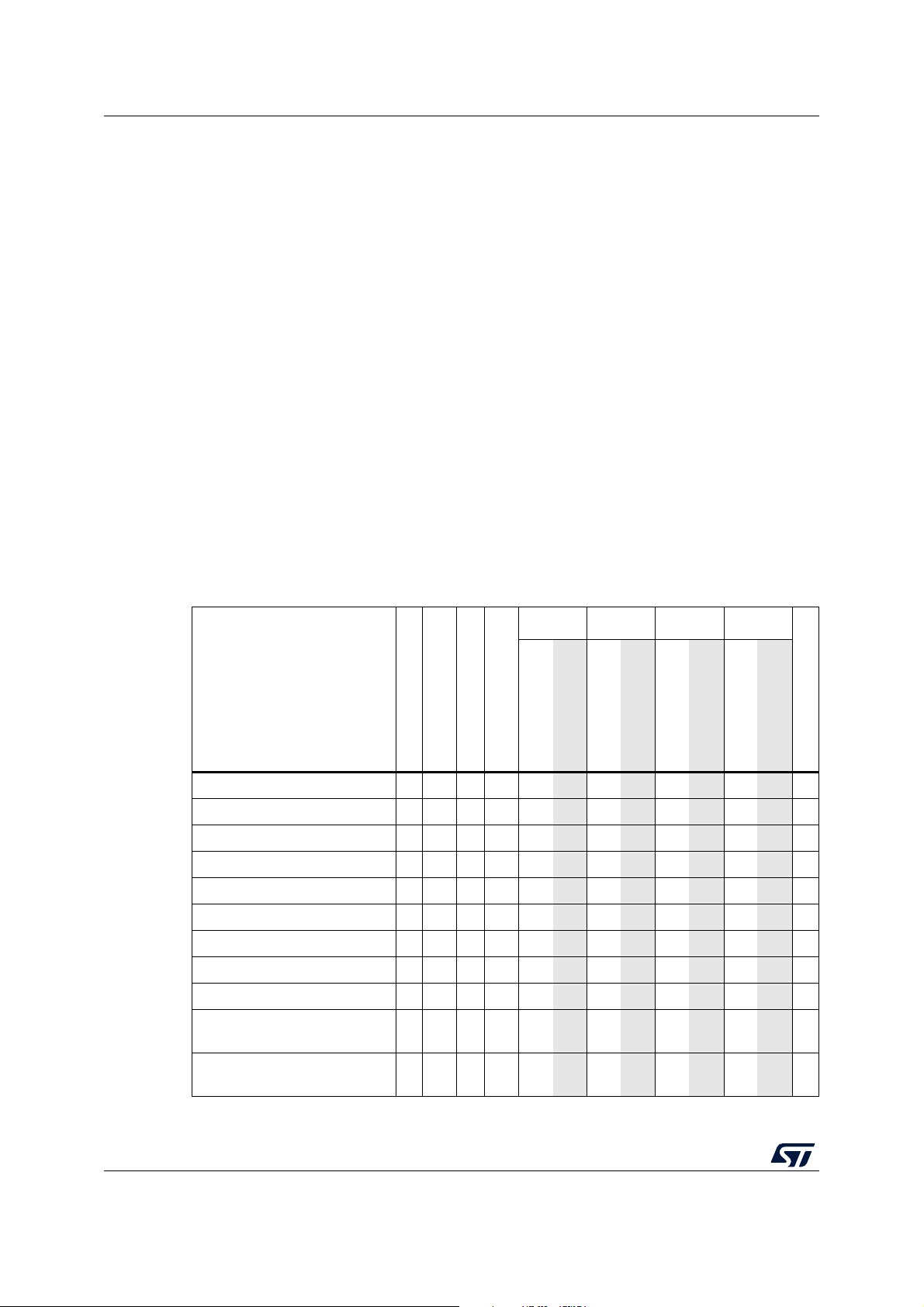
Tab l e 6 summarizes the peripheral features over all available modes. Wakeup capability is
detailed in gray cells.
Table 6. Functionalities depending on system operating mode
(1)
Stop0 Stop1 Standby Shutdow
Peripheral
Run
Sleep
Low-power run
-
Low-power sleep
Wakeup capability
-
Wakeup capability
-
-
Wakeup capability
VBAT
Wakeup capability
CPU1 Y - Y - - --------
CPU2 Y - Y - -
Radio-system (BLE) Y Y - - -
Flash memory Y Y O O R
SRAM1 Y O
SRAM2a Y O
SRAM2b Y O
(3)
(3)
(3)
(3)
YO
(3)
YO
(3)
YO
Backup registers Y Y Y Y R
Brown-out reset (BOR) Y Y Y Y Y
Brown-out SMPS
force bypass (BOR)
Programmable voltage detector
(PVD)
YYYY Y
OOO O O
--------
Y-Y-Y
(2)
- --
-R-R-R-R
R -R-O
R -R-O
R -R-O
(2)
----
(2)
----
(2)
----
-R-R-R-R
YYYYY- --
Y- ------
OOO- ----
26/121 DS13258 Rev 1
STM32WB15CC Functional overview
Table 6. Functionalities depending on system operating mode
Stop0 Stop1 Standby Shutdow
Peripheral
Peripheral voltage monitor
(PVMx; x=3)
DMAx (x=1) O O O O -
High speed internal (HSI16) O O O O O
High speed external (HSE) O O O O -
Low speed internal (LSI) O O O O O
Low speed external (LSE) O O O O O
Multi-speed internal (MSI) O O O O -
Clock security system (CSS) O O O O -
Clock security system on LSE O O O O O
RTC / Auto wakeup O O O O O
Run
Sleep
Low-power run
-
Low-power sleep
OOO O O
(4)
-
Wakeup capability
OOO- ----
--------
(4)
-O
--------
-O-O----
-O-O-O-O
--------
--------
OOOOO- --
OOOOOOOO
(1)
(continued)
VBAT
Wakeup capability
Wakeup capability
-
-
Wakeup capability
------
Number of RTC tamper pins 1 1 1 1 1
USART1 O O O O O
Low-power UART (LPUART) O O O O O
I2C1 O O O O O
SPIx (x=1) O O O O -
ADC1 O O O O -
COMPx (x=1) O O O O O
Temperature sensor O O O O -
Timers (TIMx) O O O O -
Low-power timer 1 (LPTIM1) O O O O O
Low-power timer 2 (LPTIM2) O O O O O
Independent watchdog (IWDG) O O O O O
Window watchdog (WWDG) O O O O -
SysTick timer O O O O -
Touch sensing controller (TSC) O O O O -
True random number generator
(RNG)
OO - - -
O1O1O1O1
(5)O(5)O(5)O(5)
(5)O(5)O(5)O(5)
(6)O(6)O(6)O(6)
- ----
- ----
- ----
--------
--------
OOO- ----
--------
--------
OOO- ----
OOO- ----
OOOOO- --
--------
--------
--------
--------
AES hardware accelerator O O O O - --------
CRC calculation unit O O O O -
--------
DS13258 Rev 1 27/121
44
Functional overview STM32WB15CC
Table 6. Functionalities depending on system operating mode
(1)
(continued)
Stop0 Stop1 Standby Shutdow
Peripheral
Run
Sleep
Low-power run
-
Low-power sleep
Wakeup capability
-
Wakeup capability
-
Wakeup capability
-
Wakeup capability
IPCC O - O - - --------
HSEM O - O - -
PKA O O O O -
GPIOs O O O O O
1. Legend: Y = Yes (enabled). O = Optional (disabled by default, can be enabled by software).
R = data retained. - = Not available. Gray cells indicate Wakeup capability.
2. The SRAM1, SRAM2a and SRAM2b content needs to be retained via the PWR_CR3.RRS bit.
3. The SRAM clock can be gated on or off.
4. Some peripherals with wakeup from Stop capability can request HSI16 to be enabled. In this case, HSI16
is woken up by the peripheral, and only feeds the peripheral which requested it. HSI16 is automatically put
off when the peripheral does not need it anymore.
5. UART and LPUART reception is functional in Stop mode, and generates a wakeup interrupt on Start,
address match or received frame event.
6. I2C address detection is functional in Stop mode, and generates a wakeup interrupt in case of address
match.
7. I/Os can be configured with internal pull-up, pull-down or floating in Standby mode.
8. The I/Os with wakeup from Standby/Shutdown capability are PA0 and PA2.
9. I/Os can be configured with internal pull-up, pull-down or floating in Shutdown mode but the configuration is
lost when exiting the Shutdown mode.
--------
--------
OOO
(7)
2
pins
(8)
(9)
2
pins
(9)
-
VBAT
28/121 DS13258 Rev 1

Table 7. STM32WB15CC modes overview
Mode Regulator CPU1 Flash SRAM Clocks DMA and Peripherals Wakeup source Consumption
Run MR Yes ON
LPRun LPR Yes ON
Sleep MR No ON
(2)
(2)
(2)
ON Any All N/A 91 µA/MHz N/A
Any
ON
except
All except RF and RNG N/A 90 µA/MHz TBD µs
PLL
ON
(3)
Any All
Any interrupt
or event
28 µA/MHz TBD cycles
(1)
STM32WB15CC Functional overview
Wakeup time
Any
except
All except RF and RNG
LPSleep LPR No ON
(2)
ON
(3)
PLL
RF, BOR, PVD, PVM, RTC,
DS13258 Rev 1 29/121
Stop 0 MR No OFF ON
LSE, LSI,
(4)
HSE
(5)
HSI16
,
IWDG, COMPx (x=1),
USART1
I2C1
(6)
(7)
, LPTIMx (x=1, 2), SMPS
All other peripherals are frozen.
RF, BOR, PVD, PVM, RTC,
IWDG, COMPx (x=1),
USART1
I2C1
(6)
(7)
, LPTIMx (x=1, 2)
Stop 1 LPR No OFF ON
LSE, LSI,
(4)
HSE
(5)
HSI16
,
All other peripherals are frozen.
RF, BOR, RTC, IWDG
All other peripherals are
powered off.
I/O configuration can be floating,
Standby
LPR
SRAMs
ON
No OFF
OFF OFF
LSE, LSI
pull-up or pull-down
RTC
All other peripherals are
Shutdown OFF No OFF OFF LSE
powered off.
I/O configuration can be floating,
pull-up or pull-down
1. Typical current at VDD = 1.8 V, 25 °C. for STOPx, SHUTDOWN and Standby, else VDD = 3.3 V, 25 °C.
, LPUART1
, LPUART1
(9)
(6)
(6)
Any interrupt
or event
Reset pin, all I/Os, RF,
BOR, PVD, PVM,
RTC, IWDG, COMPx
,
(x=1), USART1,
LPUART1, I2C1,
LPTIMx (x=1, 2)
Reset pin, all I/Os
RF, BOR, PVD, PVM,
RTC, IWDG, COMPx
,
(x=1), USART1,
LPUART1, I2C1,
LPTIMx (x=1, 2)
RF, Reset pin
Two I/Os (WKUPx)
BOR, RTC, IWDG
Two I/Os (WKUPx)
RTC
27 µA/MHz TBD cycles
100 µA TBD µs
3.05 µA w/o RTC
3.35 µA w RTC
0.335 µA w/o RTC
0.61 µA w RTC
(8)
0.243 µA w/o RTC
0.518 µA w RTC
(8)
0.012 µA w/o RTC
,
0.210 µA w/ RTC
TBD µs
TBD µs
-

30/121 DS13258 Rev 1
2. The Flash memory controller can be placed in power-down mode if the RF subsystem is not in use and all the program is run from the SRAM.
3. The SRAM1 and SRAM2 clocks can be gated off independently.
4. HSE (32 MHz) automatically used when RF activity is needed by the RF subsystem.
5. HSI16 (16 MHz) automatically used by some peripherals.
6. U(S)ART and LPUART reception is functional in Stop mode, and generates a wakeup interrupt on Start, Address match or Received frame event.
7. I2C address detection is functional in Stop mode, and generates a wakeup interrupt in case of address match.
8. I/Os with wakeup from Standby/Shutdown capability: PA0, PA2.
9. I/Os can be configured with internal pull-up, pull-down or floating but the configuration is lost immediately when exiting the Shutdown mode.
Functional overview STM32WB15CC

STM32WB15CC Functional overview
3.7.6 Reset mode
To improve the consumption under reset, the I/Os state under and after reset is “analog
state” (the I/O Schmitt trigger is disabled). In addition, the internal reset pull-up is
deactivated when the reset source is internal.
3.8 VBAT operation
The VBAT pin allows to power the device VBAT domain (RTC, LSE and Backup registers)
from an external battery, an external supercapacitor, or from V
when no external battery
DD
nor an external supercapacitor are present. One anti-tamper detection pin is available in
VBAT mode.
VBAT operation is automatically activated when VDD is not present.
An internal VBAT battery charging circuit is embedded and can be activated when VDD is
present.
Note: When the microcontroller is supplied only from VBAT, external interrupts and RTC
alarm/events do not exit it from VBAT operation.
3.9 Interconnect matrix
TIMx
COMPx
Several peripherals have direct connections between them. This allows autonomous
communication between peripherals, saving CPU1 resources and, consequently, reducing
power supply consumption. In addition, these hardware connections result in fast and
predictable latency.
Depending on peripherals, these interconnections can operate in Run, Sleep, Low-power
run and Sleep, Stop 0 and Stop 1 modes.
Table 8. STM32WB15CC CPU1 peripherals interconnect matrix
Source Destination Action
TIMx Timers synchronization or chaining Y Y Y Y -
ADC1 Conversion triggers Y Y Y Y -
DMA Memory to memory transfer trigger Y Y Y Y -
COMP1 Comparator output blanking Y Y Y Y -
TIM1
TIM2
LPTIMERx
Timer input channel, trigger, break from
analog signals comparison
Low-power timer triggered by analog
signals comparison
Run
Sleep
Low-power run
YYYY -
YYYYY
Low-power
Stop 0 / Stop 1
ADC1 TIM1 Timer triggered by analog watchdog Y Y Y Y -
RTC
LPTIMERx
Low-power timer triggered by RTC
alarms or tampers
DS13258 Rev 1 31/121
YYYYY
44

Functional overview STM32WB15CC
Table 8. STM32WB15CC CPU1 peripherals interconnect matrix (continued)
Source Destination Action
All clock sources
(internal and external)
CSS
CPU (hard fault)
SRAM (parity error)
Flash memory (ECC error)
COMP1
PVD
GPIO
Run
Sleep
Low-power
Low-power run
TIM2
TIM1 Timer break Y Y Y Y -
TIMx External trigger Y Y Y Y -
LPTIMERx External trigger Y Y Y Y Y
ADC1 Conversion external trigger Y Y Y Y -
Clock source used as input channel for
RC measurement and trimming
YYYY -
Stop 0 / Stop 1
32/121 DS13258 Rev 1

STM32WB15CC Functional overview
3.10 Clocks and startup
The STM32WB15CC device integrates several clock sources:
LSE: 32.768 kHz external oscillator, for accurate RTC and calibration with other
embedded RC oscillators
LSI1: 32 kHz on-chip low-consumption RC oscillator
LSI2: TBD kHz (untrimmable), on-chip temperature stable RC oscillator
HSE: high quality 32 MHz external oscillator with trimming, needed by the RF
subsystem
HSI16: 16 MHz high accuracy on-chip RC oscillator
MSI: 100 kHz to 48 MHz multiple speed on-chip low power oscillator, can be trimmed
using the LSE signal
The clock controller (see Figure 7) distributes the clocks coming from the different
oscillators to the core and the peripherals including the RF subsystem. It also manages
clock gating for low power modes and ensures clock robustness. It features:
Clock prescaler: to get the best trade-off between speed and current consumption,
the clock frequency to the CPU and peripherals can be adjusted by a programmable
prescaler
Safe clock switching: clock sources can be changed safely on the fly in run mode
through a configuration register.
Clock management: to reduce power consumption, the clock controller can stop the
clock to the core, individual peripherals or memory.
System clock source: four different clock sources can be used to drive the master
clock SYSCLK:
– 16 MHz high-speed internal RC oscillator (HSI16), trimmable by software, that can
supply a PLL
– Multispeed internal RC oscillator (MSI), trimmable by software, able to generate
12 frequencies from 100 kHz to 48 MHz. When a 32.768 kHz clock source is
available in the system (LSE), the MSI frequency can be automatically trimmed by
hardware to reach better than ±0.25% accuracy. The MSI can supply a PLL.
– System PLL that can be fed by HSE, HSI16 or MSI, with a maximum frequency of
64 MHz.
Auxiliary clock source: two ultralow-power clock sources that can be used to drive
the real-time clock:
– 32.768 kHz low-speed external crystal (LSE), supporting four drive capability
modes. The LSE can also be configured in bypass mode for an external clock.
– 32 kHz low-speed internal RC (LSI1), also used to drive the independent
watchdog. The LSI1 clock accuracy is ±5%.
– TBD kHz low-speed internal RC (LSI2), with TBD stability over temperature.
Peripheral clock sources: Several peripherals (RNG, USARTs, I2C, LPTimers, ADC)
have their own independent clock whatever the system clock. A PLL having three
DS13258 Rev 1 33/121
44

Functional overview STM32WB15CC
independent outputs for the highest flexibility can generate independent clocks for the
ADC and the RNG.
Startup clock: after reset, the microcontroller restarts by default with an internal 4 MHz
clock (MSI). The prescaler ratio and clock source can be changed by the application
program as soon as the code execution starts.
Clock security system (CSS): this feature can be enabled by software. If an HSE
clock failure occurs, the master clock is automatically switched to HSI16 and a software
interrupt is generated if enabled. LSE failure can also be detected and an interrupt
generated.
Clock-out capability:
– MCO: microcontroller clock output: it outputs one of the internal clocks for
external use by the application. Low frequency clocks (LSIx, LSE) are available
down to Stop 1 low power state.
– LSCO: low speed clock output: it outputs LSI or LSE in all low-power modes
down to Standby.
Several prescalers allow the user to configure the AHB frequencies, the high speed APB
(APB2) and the low speed APB (APB1) domains. The maximum frequency of the AHB and
the APB domains is 64 MHz.
34/121 DS13258 Rev 1

STM32WB15CC Functional overview
MS53136V3
SMPS clock
source control
LSI1 RC 32 kHz
LSI2 RC 32 kHz
LSE OSC
32.768 kHz
LSCO
LSI
to IWDG
HSE OSC
32 MHz
HSE CSS
OSC_IN
OSC_OUT
HSI16 RC
16 MHz
MSI RC
100 kHz - 48 MHz
MCO
/1 - 16
/32
LSE CSS
/32
PLL
/P
/R
/Q
/M
SYSCLK
MSI
MSI
HSI
HSI16
HSE
PRE
HSE
PLLRCLK
PLLRCLK
LSE
LSI2
LSI1
SYS clock
source control
SYSCLK
MSI
HSI16
HSEPRE
HCLK1
HCLK2
HCLK4
APB1
PPRE1
/1,2,4,8,16
to CPU1, AHB1, AHB2 and SRAM1
to CPU1 FCLK
/8
to CPU1 system timer
APB2
PPRE2
/1,2,4,8,16
PCLK1
PCLK2
to CPU2
to CPU2 FCLK
/8
to CPU2 system timer
to AHB4, Flash memory and SRAM2
to APB1 TIMx
to APB2 TIMx
to USART1
to LPTIMx
to LPUART1
to ADC
to RTC
x1 or
x2
x1 or
x2
to I2C1
PCLKn
SYSCLK
HSI16
HSI16
PCLKn
LSI
LSE
PLLPCLK
SYSCLK
PCLKn
LSE
to BLE wakeup
/2
HCLK5
HSI
HSE
to AHB5
to APB3
to APB2
to APB1
to RF
SYSCLK
MSI
PLLQCLK
PLLRCLK
OSC32_IN
OSC32_OUT
LSI
LSE
LSE
MSI
HSI
HSE
SMPSDIV
/1,2,3,4,6,8,12
to SMPS
/2
CPU1
HPRE
/1,2,...,512
AHBS
SHDHPRE
/1,2,...,512
CPU2
C2HPRE
1,2,...,512
HSI16
/3
to RNG
LSI
LSE
HSE PRE
/1,2
SMPSDIV
/1,2,4
HSI_V33
HSI
PLLPCLK
xN
Figure 7. Clock tree
3.11 General-purpose inputs/outputs (GPIOs)
Each of the GPIO pins can be configured by software as output (push-pull or open-drain), as
input (with or without pull-up or pull-down) or as peripheral alternate function. Most of the
GPIO pins are shared with digital or analog alternate functions. Fast I/O toggling can be
achieved thanks to their mapping on the AHB2 bus.
The I/Os alternate function configuration can be locked, if needed, following a specific
sequence in order to avoid spurious writing to the I/Os registers.
DS13258 Rev 1 35/121
44

Functional overview STM32WB15CC
3.12 Direct memory access controller (DMA)
The device embeds one DMA. Refer to Tabl e 9 for the features implementation.
Direct memory access (DMA) is used to provide high-speed data transfer between
peripherals and memory as well as between memories. Data can be quickly moved by DMA
without any CPU action. This keeps CPU resources free for other operations.
The DMA controller has seven channels in total, a full cross matrix allows any peripheral to
be mapped on any of the available DMA channels. The DMA has an arbiter for handling the
priority between DMA requests.
The DMA supports:
seven independently configurable channels (requests)
A full cross matrix between peripherals and all the DMA channels exist. There is also a
HW trigger possibility through the DMAMUX.
Priorities between requests from DMA channels are software programmable (four
levels consisting in very high, high, medium and low) or hardware in case of equality
(request 1 has priority over request 2, etc.).
Independent source and destination transfer size (byte, half word, word), emulating
packing and unpacking. Source/destination addresses must be aligned on the data
size.
Support for circular buffer management.
Three event flags (DMA half transfer, DMA transfer complete and DMA transfer error)
logically OR-ed together in a single interrupt request for each channel.
Memory-to-memory transfer.
Peripheral-to-memory and memory-to-peripheral, and peripheral-to-peripheral
transfers.
Access to Flash memory, SRAM, APB and AHB peripherals as source and destination.
Programmable number of data to be transferred: up to 65536.
Number of regular channels 7
Table 9. DMA implementation
DMA features DMA1
A DMAMUX block makes it possible to route any peripheral source to any DMA channel.
3.13 Interrupts and events
3.13.1 Nested vectored interrupt controller (NVIC)
The device embeds a nested vectored interrupt controller able to manage 16 priority levels,
and handle up to 63 maskable interrupt channels plus the 16 interrupt lines of the
Cortex®-M4 with FPU.
36/121 DS13258 Rev 1

STM32WB15CC Functional overview
The NVIC benefits are the following:
Closely coupled NVIC gives low latency interrupt processing
Interrupt entry vector table address passed directly to the core
Allows early processing of interrupts
Processing of late arriving higher priority interrupts
Support for tail chaining
Processor state automatically saved
Interrupt entry restored on interrupt exit with no instruction overhead
The NVIC hardware block provides flexible interrupt management features with minimal
interrupt latency.
3.13.2 Extended interrupts and events controller (EXTI)
The EXTI manages wakeup through configurable and direct event inputs. It provides
wake-up requests to the Power control, and generates interrupt requests to the CPUx NVIC
and events to the CPUx event input.
Configurable events/interrupts come from peripherals able to generate a pulse, and make it
possible to select the Event/Interrupt trigger edge and/or a SW trigger.
Direct events/interrupts are coming from peripherals having their own clearing mechanism.
3.14 Analog to digital converter (ADC)
The 12-bit analog-to-digital converter has up to ten external and three internal (temperature
sensor, voltage reference, VBAT voltage measurement) channels and performs conversions
in single-shot or scan modes. In scan mode, automatic conversion is performed on a
selected group of analog inputs.
An analog watchdog feature makes possible a very precise monitoring of the converted
voltage of one, some or all selected channels. An interrupt is generated when the converted
voltage is outside the programmed thresholds.
3.14.1 Temperature sensor
The temperature sensor (TS) generates a voltage VTS that varies linearly with temperature.
The temperature sensor is internally connected to the ADC1_IN12 input channel, which is
used to convert the sensor output voltage into a digital value.
To improve the accuracy of the temperature sensor measurement, each device is
individually factory-calibrated by ST. The temperature sensor factory calibration data are
stored in the system memory area, accessible in read-only mode.
DS13258 Rev 1 37/121
44

Functional overview STM32WB15CC
Calibration value name Description Memory address
TS_CAL1
TS_CAL2
Table 10. Temperature sensor calibration values
TS ADC raw data acquired at a
temperature of 30 °C (± 5 °C),
V
DDA
TS ADC raw data acquired at a
temperature of 130 °C (± 5 °C),
V
DDA
3.14.2 Internal voltage reference (V
The internal voltage reference (VREFINT) provides a stable (bandgap) voltage output for
the ADC and the comparator. VREFINT is internally connected to the ADC1_IN13 input
channel. The precise voltage of VREFINT is individually measured for each part by ST
during production test and stored in the system memory area. It is accessible in read-only
mode.
Calibration value name Description Memory address
Table 11. Internal voltage reference calibration values
Raw data acquired at a
VREFINT
temperature of 30 °C (± 5 °C),
V
DDA
= 3.0 V (± 10 mV)
= 3.0 V (± 10 mV)
REFINT
= 3.6 V (± 10 mV)
)
0x1FFF 75A8 - 0x1FFF 75A9
0x1FFF 75CA - 0x1FFF 75CB
0x1FFF 75AA - 0x1FFF 75AB
3.15 Comparator (COMP)
The STM32WB15CC devices embeds a comparator with programmable reference voltage
(internal or external), hysteresis and speed (low speed for low-power) and with selectable
output polarity.
The reference voltage can be one of the following:
External I/O
Internal reference voltage or submultiple (1/4, 1/2, 3/4).
The comparator can wake up from Stop mode, generate interrupts and breaks for the timers
and can be also combined into a window comparator.
3.16 Touch sensing controller (TSC)
The touch sensing controller provides a simple solution for adding capacitive sensing
functionality to any application. Capacitive sensing technology is able to detect finger
presence near an electrode which is protected from direct touch by a dielectric such as
glass or plastic. The capacitive variation introduced by the finger (or any conductive object)
is measured using a proven implementation based on a surface charge transfer acquisition
principle.
The touch sensing controller is fully supported by the STMTouch touch sensing firmware
library (free to use) and enables reliable touch sensing functionality in the end application.
38/121 DS13258 Rev 1

STM32WB15CC Functional overview
The main features of the touch sensing controller are the following:
Proven and robust surface charge transfer acquisition principle
Supports up to three capacitive sensing channels
Up to eight capacitive sensing channels can be acquired in parallel offering a very good
response time
Spread spectrum feature to improve system robustness in noisy environments
Full hardware management of the charge transfer acquisition sequence
Programmable charge transfer frequency
Programmable sampling capacitor I/O pin
Programmable channel I/O pin
Programmable max count value to avoid long acquisition when a channel is faulty
Dedicated end of acquisition and max count error flags with interrupt capability
One sampling capacitor for up to three capacitive sensing channels to reduce the
system components
Compatible with proximity, touchkey, linear and rotary touch sensor implementation
Designed to operate with STMTouch touch sensing firmware library
Note: The number of capacitive sensing channels is dependent upon the package and subject to
I/O availability.
3.17 True random number generator (RNG)
The device embeds a true RNG that delivers 32-bit random numbers generated by an
integrated analog circuit.
3.18 Timers and watchdogs
The STM32WB15CC includes one advanced 16-bit timer, one general-purpose 32-bit timer,
two low-power timers, two watchdog timers and a SysTick timer.
features of the advanced control, general purpose and basic timers.
Timer
type
Advanced
control
General
purpose
Low power
Timer
TIM1 16-bits
TIM2 32-bits
LPTIM1
LPTIM2
Counter
resolution
16-bits Up 1 1
Table 12. Timer features
Counter
type
Up, down,
Up/down
Up, down,
Up/down
Prescaler
factor
Any integer
between 1
and 65536
generation
DMA
request
Yes
Table 12 compares the
Capture/
compare
channels
43
4No
Complementary
outputs
3.18.1 Advanced-control timer (TIM1)
The advanced-control timer can be seen as a three-phase PWM multiplexed on six
channels. They have complementary PWM outputs with programmable inserted
DS13258 Rev 1 39/121
44

Functional overview STM32WB15CC
dead-times. They can also be seen as complete general-purpose timers. The four
independent channels can be used for:
Input capture
Output compare
PWM generation (edge or center-aligned modes) with full modulation capability (0 to
100%)
One-pulse mode output
In debug mode, the advanced-control timer counter can be frozen and the PWM outputs
disabled to turn off any power switches driven by these outputs.
Many features are shared with those of the general-purpose TIMx timers (described in
Section 3.18.2) using the same architecture, so the advanced-control timers can work
together with the TIMx timers via the Timer Link feature for synchronization or event
chaining.
3.18.2 General-purpose timer (TIM2)
There is one synchronizable general-purpose timer embedded in the STM32WB15CC (see
Tab l e 12), it can be used to generate PWM outputs, or act as a simple time base.
TIM2
– Full-featured general-purpose timer
– Features four independent channels for input capture/output compare, PWM or
one-pulse mode output. Can work together, or with the other general-purpose
timers via the Timer Link feature for synchronization or event chaining.
– The counter can be frozen in debug mode.
– Independent DMA request generation, support of quadrature encoders.
3.18.3 Low-power timer (LPTIM1 and LPTIM2)
The device embeds two low-power timers, having an independent clock running in Stop
mode if they are clocked by LSE, LSIx or by an external clock. They are able to wakeup the
system from Stop mode.
LPTIM1 is active in Stop 0 and Stop 1 modes.
LPTIM2 is active in Stop 0 and Stop 1 modes.
The low-power timers support the following features:
16-bit up counter with 16-bit autoreload register
16-bit compare register
Configurable output: pulse, PWM
Continuous/ one shot mode
Selectable software/hardware input trigger
Selectable clock source
– Internal clock sources: LSE, either LSI1 or LSI2, HSI16 or APB clock
– External clock source over LPTIM input (working even with no internal clock
source running, used by pulse counter application)
Programmable digital glitch filter
Encoder mode (LPTIM1 only)
40/121 DS13258 Rev 1

STM32WB15CC Functional overview
3.18.4 Independent watchdog (IWDG)
The independent watchdog is based on a 12-bit downcounter and an 8-bit prescaler. It is
clocked from an independent 32
from the main clock, it can operate in Stop and Standby modes. It can be used either as a
watchdog to reset the device when a problem occurs, or as a free running timer for
application timeout management. It is hardware or software configurable through the option
bytes. The counter can be frozen in debug mode.
kHz internal RC (LSI) and as it operates independently
3.18.5 System window watchdog (WWDG)
The window watchdog is based on a 7-bit downcounter that can be set as free running. It
can be used as a watchdog to reset the device when a problem occurs. It is clocked from
the main clock. It has an early warning interrupt capability and the counter can be frozen in
debug mode.
3.18.6 SysTick timer
This timer is dedicated to real-time operating systems, but could also be used as a standard
down counter. It features:
a 24-bit down counter
autoreload capability
a maskable system interrupt generation when the counter reaches 0
a programmable clock source.
3.19 Real-time clock (RTC) and backup registers
The RTC is an independent BCD timer/counter, supporting the following features:
Calendar with subsecond, seconds, minutes, hours (12 or 24 format), week day, date,
month, year, in BCD (binary-coded decimal) format.
Automatic correction for 28, 29 (leap year), 30, and 31 days of the month.
Two programmable alarms.
On-the-fly correction from 1 to 32767 RTC clock pulses. This can be used to
synchronize it with a master clock.
Reference clock detection: a more precise second source clock (50 or 60 Hz) can be
used to enhance the calendar precision.
Digital calibration circuit with 0.95 ppm resolution, to compensate for quartz crystal
inaccuracy.
One anti-tamper detection pin with programmable filter.
Timestamp feature, which can be used to save the calendar content. This function can
be triggered by an event on the timestamp pin, or by a tamper event, or by a switch to
VBAT mode.
17-bit auto-reload wakeup timer (WUT) for periodic events with programmable
resolution and period.
The RTC and the 20 backup registers are supplied through a switch that takes power either
from the V
supply (when present) or from the VBAT pin.
DD
DS13258 Rev 1 41/121
44

Functional overview STM32WB15CC
The backup registers are 32-bit registers used to store 80 bytes of user application data
when V
power is not present. They are not reset by a system or power reset, or when the
DD
device wakes up from Standby or Shutdown mode.
The RTC clock sources can be:
a 32.768 kHz external crystal (LSE)
an external resonator or oscillator (LSE)
one of the internal low power RC oscillators (LSI1 with typical frequency of 32 kHz or
LSI2)
the high-speed external clock (HSE) divided by 32.
The RTC is functional in VBAT mode and in all low-power modes when it is clocked by the
LSE. When clocked by one of the LSIs, the RTC is not functional in VBAT mode, but is
functional in all low-power modes except Shutdown mode.
All RTC events (alarm, wakeup timer, timestamp or tamper) can generate an interrupt and
wakeup the device from the low-power modes.
3.20 Inter-integrated circuit interface (I2C)
The device embeds one I2C. Refer to Tab le 13 for the features implementation.
The I2C bus interface handles communications between the microcontroller and the serial
2
I
C bus. It controls all I2C bus-specific sequencing, protocol, arbitration and timing.
The I2C peripheral supports:
I2C-bus specification and user manual rev. 5 compatibility:
– Slave and master modes, multimaster capability
– Standard-mode (Sm), with a bitrate up to 100 kbit/s
– Fast-mode (Fm), with a bitrate up to 400 kbit/s
– Fast-mode Plus (Fm+), with a bitrate up to 1 Mbit/s and 20 mA output drive I/Os
– 7-bit and 10-bit addressing mode, multiple 7-bit slave addresses
– Programmable setup and hold times
– Optional clock stretching
System Management Bus (SMBus) specification rev 2.0 compatibility:
– Hardware PEC (packet error checking) generation and verification with ACK
control
– Address resolution protocol (ARP) support
– SMBus alert
Power System Management Protocol (PMBus
™
) specification rev 1.1 compatibility
Independent clock: a choice of independent clock sources allowing the I2C
communication speed to be independent from the PCLK reprogramming. Refer to
Figure 7: Clock tree.
Wakeup from Stop mode on address match
Programmable analog and digital noise filters
1-byte buffer with DMA capability
42/121 DS13258 Rev 1

STM32WB15CC Functional overview
Standard-mode (up to 100 kbit/s) X
Fast-mode (up to 400 kbit/s) X
Fast-mode Plus with 20mA output drive I/Os (up to 1 Mbit/s) X
Programmable analog and digital noise filters X
SMBus/PMBus hardware support X
Independent clock X
Wakeup from Stop 0 / Stop 1 mode on address match X
1. X: supported.
Table 13. I2C implementation
I2C features
(1)
I2C1
3.21 Universal synchronous/asynchronous receiver transmitter (USART)
The device embeds one universal synchronous receiver transmitter.
This interface provides asynchronous communication, IrDA SIR ENDEC support,
multiprocessor communication mode, single-wire half-duplex communication mode and has
LIN Master/Slave capability. It provides hardware management of the CTS and RTS signals,
and RS485 driver enable.
The USART is able to communicate at speeds of up to 4 Mbit/s, and also provides Smart
Card mode (ISO 7816 compliant) and SPI-like communication capability.
The USART supports synchronous operation (SPI mode), and can be used as an SPI
master.
The USART has a clock domain independent from the CPU clock, allowing it to wake up the
MCU from Stop mode using baudrates up to 200
kbaud. The wake up events from Stop
mode are programmable and can be:
the start bit detection
any received data frame
a specific programmed data frame.
The USART interface can be served by the DMA controller.
3.22 Low-power universal asynchronous receiver transmitter (LPUART)
The device embeds one Low-Power UART, enabling asynchronous serial communication
with minimum power consumption. The LPUART supports half duplex single wire
communication and modem operations (CTS/RTS), allowing multiprocessor
communication.
DS13258 Rev 1 43/121
44

Functional overview STM32WB15CC
The LPUART has a clock domain independent from the CPU clock, and can wakeup the
system from Stop mode using baudrates up to 220
mode are programmable and can be:
the start bit detection
any received data frame
a specific programmed data frame.
Only a 32.768 kHz clock (LSE) is needed for LPUART communication up to 9600 baud.
Therefore, even in Stop mode, the LPUART can wait for an incoming frame while having an
extremely low energy consumption. Higher speed clock can be used to reach higher
baudrates.
The LPUART interfaces can be served by the DMA controller.
kbaud. The wake up events from Stop
3.23 Serial peripheral interface (SPI1)
The SPI interface enables communication up to 32 Mbit/s in master and up to 24 Mbit/s in
slave modes, in half-duplex, full-duplex and simplex modes. The 3-bit prescaler gives 8
master mode frequencies and the frame size is configurable from 4 bits to 16 bits. The SPI
interface support NSS pulse mode, TI mode and Hardware CRC calculation.
The SPI interface can be served by the DMA controller.
3.24 Development support
3.24.1 Serial wire JTAG debug port (SWJ-DP)
The Arm® SWJ-DP interface is embedded, and is a combined JTAG and serial wire debug
port that enables either a serial wire debug or a JTAG probe to be connected to the target.
Debug is performed using only two pins instead of the five required by the JTAG (JTAG pins
can then be reused as GPIOs with alternate function): the JTAG TMS and TCK pins are
shared with SWDIO and SWCLK, respectively, and a specific sequence on the TMS pin is
used to switch between JTAG-DP and SW-DP.
44/121 DS13258 Rev 1
STM32WB15CC Pinouts and pin description
MS53545V1
UFQFPN48
1
2
3
4
5
6
7
8
9
10
11
12
VBAT
PC14-OSC32_IN
PC15-OSC32_OUT
PH3-BOOT0
PB8
PB9
NRST
VDDA
PA0
PA1
PA2
PA3
36
35
34
33
32
31
30
29
28
27
26
25
393740
38
45
43
41
484746
44
42
222421
23
16
18
20
131415
17
19
PA4
PA5
PA8
VDD
OSC_OUT
PA6
PA7
RF1
PA9
PB2
VSSRF
VDDRF
PA10
VDD
VDDSMPS
VLXSMPS
VSSSMPS
VFBSMPS
PE4
PB1
PB0
AT1
AT0
OSC_IN
VDD
PB7
PB4
PA14
PA11
PB6
PB5
VDD
PB3
PA15
PA13
PA12
MS53559V1
UFQFPN48E
1
2
3
4
5
6
7
8
9
10
11
12
PC14-OSC32_IN
PC15-OSC32_OUT
PB10
PH3-BOOT0
PB8
PB9
PB11-NRST
VDDA
PA0
PA1
PA2
PA3
36
35
34
33
32
31
30
29
28
27
26
25
393740
38
45
43
41
484746
44
42
222421
23
16
18
20
131415
17
19
PB12
PA4
PA7
PB2
OSC_OUT
PA5
PA6
VDD
PA8
PA9
RF1
VDDRF
PA10
PB15
PB14
VDD
VDD
PE4
PB13
PB1
PB0
AT1
AT0
OSC_IN
VDD
PB7
PB4
PA14
PA11
PB6
PB5
PC1
PB3
PA15
PA13
PA12
4 Pinouts and pin description
Figure 8. STM32WB15CCU UFQFPN48 pinout
1. The above figure shows the package top view.
2. The exposed pad must be connected to ground plane.
Figure 9. STM32WB15CCU UFQFPN48E pinout
(1) (2)
(1) (2)
1. The above figure shows the package top view.
2. The exposed pad must be connected to ground plane.
DS13258 Rev 1 45/121
54
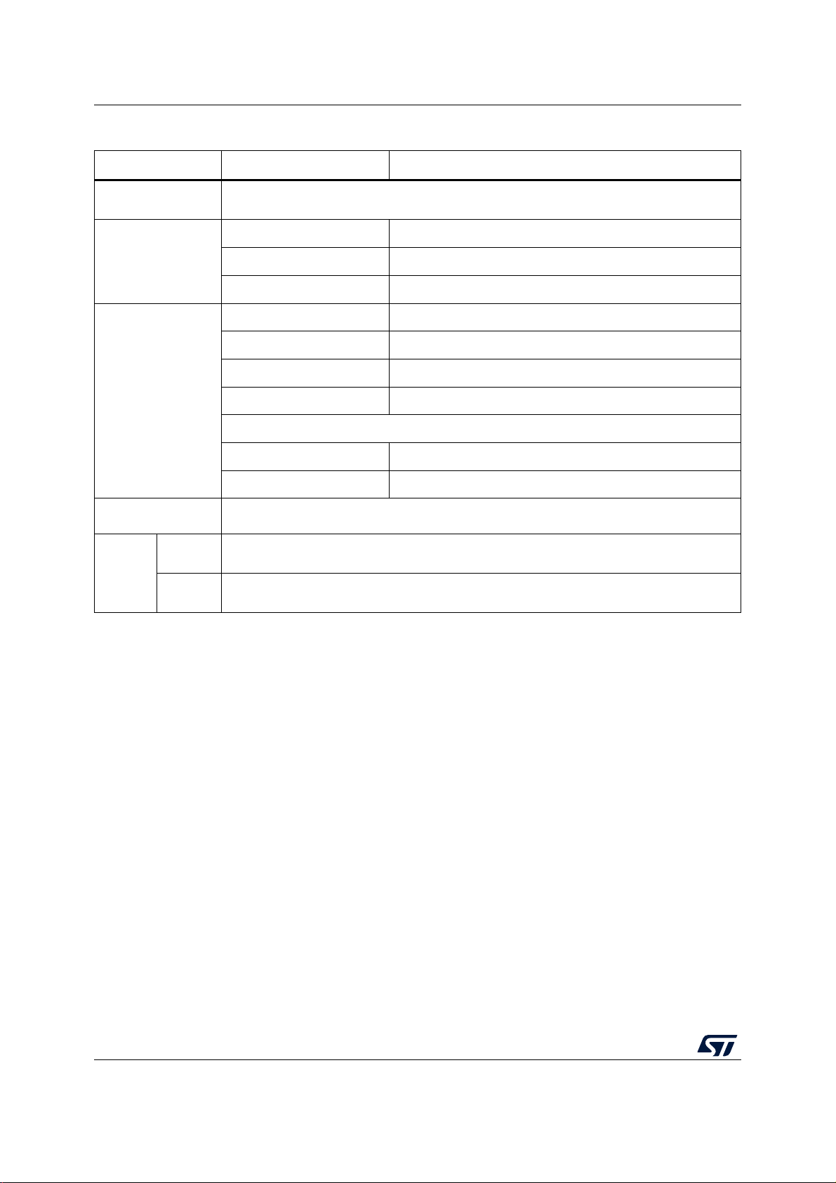
Pinouts and pin description STM32WB15CC
Table 14. Legend/abbreviations used in the pinout table
Name Abbreviation Definition
Pin name
Pin type
I/O structure
Notes Unless otherwise specified by a note, all I/Os are set as analog inputs during and after reset.
Unless otherwise specified in brackets below the pin name, the pin function during and after
reset is the same as the actual pin name
S Supply pin
I Input only pin
I/O Input / output pin
FT 5 V tolerant I/O
TT 3.6 V tolerant I/O
RF RF I/O
RST Bidirectional reset pin with weak pull-up resistor
Option for TT or FT I/Os
_a
_f
(2) (3)
(1)
I/O, Fm+ capable
I/O, with analog switch function supplied by V
DDA
Alternate
Pin
functions
functions
Additional
functions
1. The related I/O structures in Table 15 are FT_f and FT_fa.
2. The related I/O structures in Table 15 are FT_a, FT_la, FT_fa and TT_a.
3. The analog switch for the TSC function is supplied by V
Functions selected through GPIOx_AFR registers
Functions directly selected/enabled through peripheral registers
.
DD
46/121 DS13258 Rev 1

STM32WB15CC Pinouts and pin description
Table 15. STM32WB15CC pin definitions
Pin
Number
UFQFPN48
after reset)
UFQFPN48E
Name
(function
Type
Notes
I/O structures
Alternate functions Additional functions
1 - VBAT S - - - -
21
32
PC14-
OSC32_IN
PC15-
OSC32_OUT
I/O FT
I/O FT
(1)
CM4_EVENTOUT OSC32_IN
(1)
CM4_EVENTOUT OSC32_OUT
- 3 PB10 I/O FT - TSC_G3_IO2, CM4_EVENTOUT -
(2)
4 4 PH3-BOOT0 I/O FT - LSCO
5 5 PB8 I/O FT_f -
6 6 PB9 I/O FT_f -
TIM1_CH2N, I2C1_SCL, TSC_G7_IO3,
CM4_EVENTOUT
TIM1_CH3N, I2C1_SDA, TSC_G7_IO4,
CM4_EVENTOUT
, CM4_EVENTOUT -
7 7 NRST(PB11) I/O FT - - -
8 8 VDDA S - - - -
-
-
99 PA0 I/OFT_a-
10 10 PA1 I/O FT_a -
11 11 PA2 I/ O F T_a -
12 12 PA3 I/O FT_a -
- 13 PB12 I/O FT -
13 14 PA4 I/O FT_a -
14 15 PA5 I/O FT_a -
15 16 PA6 I/O FT_a -
16 17 PA7 I/O FT_a -
17 18 PA8 I/O FT_a -
TIM2_CH1, COMP1_OUT, TIM2_ETR,
CM4_EVENTOUT
TIM2_CH2, I2C1_SMBA, SPI1_SCK,
CM4_EVENTOUT
(2)
LSCO
, TIM2_CH3, LPUART1_TX,
CM4_EVENTOUT
TIM2_CH4, LPUART1_RX,
CM4_EVENTOUT
TIM2_CH2, TSC_G1_IO1,
CM4_EVENTOUT
SPI1_NSS(boot), LPTIM2_OUT,
CM4_EVENTOUT
TIM2_CH1, TIM2_ETR, SPI1_MOSI,
SPI1_SCK(boot), LPTIM2_ETR,
CM4_EVENTOUT
TIM1_BKIN, SPI1_MISO(boot),
LPUART1_CTS, CM4_EVENTOUT
TIM1_CH1N, SPI1_MOSI(boot),
CM4_EVENTOUT
MCO, TIM1_CH1, USART1_CK,
LPTIM2_OUT, CM4_EVENTOUT
COMP1_INM,
ADC1_IN5,
RTC_TAMP2/WKUP1
COMP1_INP,
ADC1_IN6
ADC1_IN7, WKUP4
ADC1_IN8
-
COMP1_INM,
ADC1_IN9
COMP1_INM,
ADC1_IN10
ADC1_IN11
ADC1_IN2
ADC1_IN3
DS13258 Rev 1 47/121
54

Pinouts and pin description STM32WB15CC
Table 15. STM32WB15CC pin definitions (continued)
Pin
Number
Name
UFQFPN48
UFQFPN48E
(function
after reset)
Type
I/O structures
18 19 PA9 I/O FT_fa -
19 20 PB2 I/O FT_a -
Notes
TIM1_CH2, I2C1_SCL, USART1_TX(boot),
CM4_EVENTOUT
RTC_OUT, LPTIM1_OUT, SPI1_NSS,
CM4_EVENTOUT
Alternate functions Additional functions
COMP1_INM,
ADC1_IN4
COMP1_INP
20 21 VDD S - - - -
(3)
21 22 RF1 I/O RF
-- -
22 - VSSRF S - - - -
23 23 VDDRF S - - - -
24 24 OSC_OUT O RF
(4)
--
25 25 OSC_IN I RF - - -
26 26 AT0 I/O RF
27 27 AT1 I/O RF
28 28 PB0 I/O TT
29 29 PB1 I/O TT
- 30 PB13 I/O FT -
(5)
(5)
RF_TX_MOD_EXT_PA, COMP1_OUT,
(6)
CM4_EVENTOUT
LPUART1_RTS_DE, LPTIM2_IN1,
(6)
CM4_EVENTOUT
TIM2_CH3, TSC_G1_IO2,
CM4_EVENTOUT
--
--
30 31 PE4 I/O FT - CM4_EVENTOUT -
31 - VFBSMPS S - - - -
-
-
-
32 - VSSSMPS S - - - -
33 - VLXSMPS S - - - -
34 - VDDSMPS S - - - -
35 - VDD S - - - -
32 VDD S - - - -
33 VDD S - - - -
- 34 PB14 I/O FT - TIM1_CH1, CM4_EVENTOUT -
- 35 PB15 I/O FT - TIM2_CH1, CM4_EVENTOUT -
36 36 PA10 I/O FT_f -
37 37 PA11 I/O FT -
TIM1_CH3, I2C1_SDA, USART1_RX(boot),
TSC_G7_IO2, CM4_EVENTOUT
TIM1_CH4, TIM1_BKIN2, SPI1_MISO,
USART1_CTS, CM4_EVENTOUT
48/121 DS13258 Rev 1
-
-

STM32WB15CC Pinouts and pin description
Table 15. STM32WB15CC pin definitions (continued)
Pin
Number
Name
UFQFPN48
UFQFPN48E
(function
after reset)
Type
I/O structures
38 38 PA12 I/O FT -
39 39 PA13 I/O FT
Notes
TIM1_ETR, SPI1_MOSI, USART1_RTS,
LPUART1_RX, CM4_EVENTOUT
JTMS-SWDIO, SPI1_MOSI, TSC_G7_IO1,
(7)
CM4_EVENTOUT
Alternate functions Additional functions
-
-
40 - VDD S - - - -
- 40 PC1 I/O FT - TSC_G3_IO3, CM4_EVENTOUT -
41 41 PA14 I/O FT
42 42 PA15 I/O FT
(7)
SPI1_NSS, CM4_EVENTOUT
JTDI, TIM2_CH1, TIM2_ETR, SPI1_NSS,
(7)
MCO, TSC_G3_IO1, CM4_EVENTOUT
-
-
JTCK-SWCLK, LPTIM1_OUT, I2C1_SMBA,
JTDO-TRACESWO, TIM2_CH2,
43 43 PB3 I/O FT -
SPI1_SCK, USART1_RTS,
-
CM4_EVENTOUT
NJTRST, SPI1_MISO, USART1_CTS,
44 44 PB4 I/O FT
45 45 PB5
(8)
I/O FT -
(7)
TSC_G2_IO1, CM4_EVENTOUT
LPTIM1_IN1, I2C1_SMBA, SPI1_MOSI,
USART1_CK, LPUART1_TX,
-
-
TSC_G2_IO2, CM4_EVENTOUT
MCO, LPTIM1_ETR, I2C1_SCL(boot),
46 46 PB6 I/O FT_f -
SPI1_NSS, USART1_TX, TSC_G2_IO3,
-
CM4_EVENTOUT
LPTIM1_IN2, TIM1_BKIN, I2C1_SDA(boot),
47 47 PB7 I/O FT_f -
USART1_RX, TSC_G2_IO4, TIM1_CH3,
PVD_IN
CM4_EVENTOUT
48 48 VDD S - - - -
1. PC14 and PC15 are supplied through the power switch. As this switch only sinks a limited current (3 mA), the use of PC14
and PC15 GPIOs in output mode is limited:
- the speed must not exceed 2 MHz with a maximum load of 30 pF
- these GPIOs must not be used as current sources (e.g. to drive an LED).
After a Backup domain power-up PC14 and PC15 operate as GPIOs. Their function depends on the content of the RTC
registers not reset by the system reset. For details on how to manage these GPIOs, refer to the Backup domain and RTC
register description in RM0473, available on www.st.com.
2. The clock on LSCO is available in Run and Stop modes, and on PA2 in Standby and Shutdown modes.
3. RF pin, use the nominal PCB layout.
4. 32 MHz oscillator pins, use the nominal PCB layout according to reference design (see AN5165 available on www.st.com).
5. Reserved for production, must be kept unconnected.
6. High frequency (above 32 KHz) may impact RF performance. Set output speed GPIOB_OSPEEDRy[1:0] to 00 (y = 0 and
1) during RF operation.
7. After reset, this pin is configured as JTAG/SW debug alternate function, and the internal pull-up on PA15, PA13 and PB4
pins and the internal pull-down on PA14 pin are activated.
DS13258 Rev 1 49/121
54

Pinouts and pin description STM32WB15CC
8. PB5 pin is configured as input with pull up active under reset if NRST pin is active (external or internal reset).
50/121 DS13258 Rev 1

Port
Table 16. Alternate functions
AF0 AF1 AF2 AF3 AF4 AF5 AF6 AF7 AF8 AF9 AF12 AF14 AF15
SYS_AF
LPTIM1/
TIM1/2
TIM1/2 TIM1
I2C1/
SPI1
SPI1
RF/
SYS_AF
USART1 LPUART1 TSC
COMP1/
TIM1
LPTIM2/
TIM2
STM32WB15CC Pinouts and pin description
EVENTOUT
DS13258 Rev 1 51/121
PA0
PA1
PA2
PA3
PA4
PA5
PA6
PA7
-
-
LSCO
-
- - - - SPI1_NSS - - - - -
-
-
-
A
PA8
PA9
PA1 0
PA11
PA1 2
PA1 3
PA1 4
PA1 5
MCO
-
-
-
-
JTMS-
SWDIO
JTCK-
SWCLK
JTDI
TIM2_
CH1
TIM2_
CH2
TIM2_
CH3
TIM2_
CH4
TIM2_
CH1
TIM1_
BKIN
TIM1_
CH1N
TIM1_
CH1
TIM1_
CH2
TIM1_
CH3
TIM1_
CH4
TIM1_
ETR
- - - - SPI1_MOSI - - -
LPTIM1_
OUT
TIM2_
CH1
-- - - - - - -
--
-- - - - -
-- - - - -
TIM2_
ETR
- - SPI1_MISO - -
- - - SPI1_MOSI - - - - - -
-- - - -
--
--
TIM1_
BKIN2
- - - SPI1_MOSI -
--
TIM2_
ETR
- SPI1_MOSI SPI1_SCK - - - - -
- - SPI1_MISO -
- SPI1_NSS MCO - -
I2C1_
SMBA
I2C1_
SCL
I2C1_
SDA
I2C1_
SMBA
SPI1_SCK - - - - - -
USART1_
CK
--
--
SPI1_NSS - - - - - -
USART1_
TX
USART1_
RX
USART1_
CTS
USART1_
RTS
LPUART1_
TX
LPUART1_
RX
LPUART1_
CTS
---
--- -
-
--- -
LPUART1_
RX
TSC_
G7_IO2
TSC_
G7_IO1
TSC_
G3_IO1
COMP1_
OUT
-- -
-- -
-- -
--
-- -
--
--
TIM2_
ETR
LPTIM2_
OUT
LPTIM2_
ETR
LPTIM2_
OUT
EVENTOUT
EVENTOUT
EVENTOUT
EVENTOUT
EVENTOUT
EVENTOUT
EVENTOUT
EVENTOUT
EVENTOUT
EVENTOUT
EVENTOUT
EVENTOUT
EVENTOUT
EVENTOUT
EVENTOUT
EVENTOUT
CM4_
CM4_
CM4_
CM4_
CM4_
CM4_
CM4_
CM4_
CM4_
CM4_
CM4_
CM4_
CM4_
CM4_
CM4_
CM4_

52/121 DS13258 Rev 1
Port
Table 16. Alternate functions (continued)
AF0 AF1 AF2 AF3 AF4 AF5 AF6 AF7 AF8 AF9 AF12 AF14 AF15
SYS_AF
LPTIM1/
TIM1/2
TIM1/2 TIM1
I2C1/
SPI1
SPI1
RF/
SYS_AF
USART1 LPUART1 TSC
COMP1/
TIM1
LPTIM2/
TIM2
EVENTOUT
Pinouts and pin description STM32WB15CC
PB0
PB1
PB2
PB3
PB4
PB5
PB6
B
PB7
PB8
PB9
PB10
PB12
PB13
PB14
PB15
---- - -
---- - - - -
RTC_
OUT
JTDO-
TRACE
SWO
NJTRST - - - - SPI1_MISO -
MCO
LPTIM1_
OUT
TIM2_
CH2
LPTIM1_
-
-
-
-
IN1
LPTIM1_
ETR
LPTIM1_
IN2
TIM1_
CH2N
TIM1_
CH3N
TIM2_
CH2
TIM2_
CH3
TIM1_
CH1
TIM2_
CH1
- - - SPI1_NSS - - - - - -
- - - SPI1_SCK -
--
--
- TIM1_BKIN
--
--
-- - - - - -
-- - - - - -
-- - - - - -
-- - - - - - -- -
-- - - - - - -- -
I2C1_
SMBA
I2C1_
SCL
I2C1_
SDA
I2C1_
SCL
I2C1_
SDA
SPI1_MOSI -
SPI1_NSS -
--
----
----
RF_TX_
MOD_EXT_PA
---
LPUART1_
RTS_DE
USART1_
RTS_
USART1_
CTS
USART1_CKLPUART1_TXTSC_
USART1_
TX
USART1_
RX
--- -
-
-
-
TSC_
G2_IO1
G2_IO2
TSC_
G2_IO3
TSC_
G2_IO4
TSC_
G7_IO3
TSC_
G7_IO4
TSC_
G3_IO2
TSC_
G1_IO1
TSC_
G1_IO2
COMP1_
OUT
--
TIM1_CH3 -
LPTIM2_
--
--
--
--
--
--
--
--
IN1
-
CM4_
EVENTOUT
CM4_
EVENTOUT
CM4_
EVENTOUT
CM4_
EVENTOUT
CM4_
EVENTOUT
CM4_
EVENTOUT
CM4_
EVENTOUT
CM4_
EVENTOUT
CM4_
EVENTOUT
CM4_
EVENTOUT
CM4_
EVENTOUT
CM4_
EVENTOUT
CM4_
EVENTOUT
CM4_
EVENTOUT
CM4_
EVENTOUT

Port
Table 16. Alternate functions (continued)
AF0 AF1 AF2 AF3 AF4 AF5 AF6 AF7 AF8 AF9 AF12 AF14 AF15
SYS_AF
LPTIM1/
TIM1/2
TIM1/2 TIM1
I2C1/
SPI1
SPI1
RF/
SYS_AF
USART1 LPUART1 TSC
COMP1/
TIM1
LPTIM2/
TIM2
EVENTOUT
STM32WB15CC Pinouts and pin description
DS13258 Rev 1 53/121
PC1
PC14
C
PC15
PE4
E
PH3
H
---- - - - --
---- - - - -----
---- - - - -----
---- - - - -----
LSCO - - - - - - - - - - -
TSC_G3
_IO3
--
CM4_
EVENTOUT
CM4_
EVENTOUT
CM4_
EVENTOUT
CM4_
EVENTOUT
CM4_
EVENTOUT

Memory mapping STM32WB15CC
5 Memory mapping
The STM32WB15CC devices feature a single physical address space that can be accessed
by the application processor and by the RF subsystem.
A part of the Flash memory and of the SRAM2a and SRAM2b memories are made secure,
exclusively accessible by the CPU2, protected against execution, read and write from CPU1
and DMA.
In case of shared resources the SW has to implement arbitration mechanism to avoid
access conflicts. This happens for peripherals Reset and clock controller (RCC), Power
controller (PWC), EXTI and Flash interface, and can be implemented using the built-in
semaphore block (HSEM).
By default the RF subsystem and CPU2 operate in secure mode. This implies that part of
the Flash and of the SRAM2 memories can only be accessed by the RF subsystem and by
the CPU2. In this case the Host processor (CPU1) has no access to these resources.
The detailed memory map and the peripheral mapping of the STM32WB15CC devices can
be found in the reference manual RM0473.
54/121 DS13258 Rev 1

STM32WB15CC Electrical characteristics
MS19210V1
MCU pin
C = 50 pF
MS19211V1
MCU pin
V
IN
6 Electrical characteristics
6.1 Parameter conditions
Unless otherwise specified, all voltages are referenced to VSS.
6.1.1 Minimum and maximum values
Unless otherwise specified, the minimum and maximum values are guaranteed in the worst
conditions of ambient temperature, supply voltage and frequencies by tests in production on
100% of the devices with an ambient temperature at T
the selected temperature range).
Data based on characterization results, design simulation and/or technology characteristics
are indicated in the table footnotes and are not tested in production. Based on
characterization, the minimum and maximum values refer to sample tests and represent the
mean value plus or minus three times the standard deviation (mean ± 3).
6.1.2 Typical values
= 25 °C and TA = TAmax (given by
A
Unless otherwise specified, typical data are based on VDD = V
T
= 25 °C. They are given only as design guidelines and are not tested.
A
Typical ADC accuracy values are determined by characterization of a batch of samples from
a standard diffusion lot over the full temperature range, where 95% of the devices have an
error less than or equal to the value indicated
6.1.3 Typical curves
Unless otherwise specified, all typical curves are given only as design guidelines and are
not tested.
6.1.4 Loading capacitor
The loading conditions used for pin parameter measurement are shown in Figure 10.
6.1.5 Pin input voltage
The input voltage measurement on a pin of the device is described in Figure 11.
Figure 10. Pin loading conditions Figure 11. Pin input voltage
(mean ± 2).
DDA
= V
DDRF
= 3 V,
DS13258 Rev 1 55/121
113

Electrical characteristics STM32WB15CC
MS53546V2
V
DD
Backup circuitry
(LSE, RTC and
backup registers)
Kernel logic
(CPU, digital
and memories
Level shifter
IO
logic
IN
OUT
Regulator
GPIOs
1.55 V to 3.6 V
n x 100 nF
+ 1 x 4.7 μF
n x VDD
VBAT
V
CORE
Power switch
V
DDIO1
ADC
COMPs
V
DDA
10 nF + 1 μF
VDDA
SMPS
Regulator
VDDSMPS
VLXSMPS
VFBSMPS
VSSSMPS
4.7 μF
V
DD
L1
(1)
Exposed pad
4.7 μF
To all modules
SMPS
Radio
100 nF
+ 100 pF
VDDRF
V
DD
V
SS
V
REF-
V
REF+
6.1.6 Power supply scheme
Figure 12. Power supply scheme
Caution: Each power supply pair (e.g. VDD / VSS, V
56/121 DS13258 Rev 1
1. The value of L1 depends upon the frequency, as indicated in Table 5: Power supply typical components.
ceramic capacitors as shown in Figure 12. These capacitors must be placed as close as
possible to (or below) the appropriate pins on the underside of the PCB to ensure the good
functionality of the device.
DDA
/ V
) must be decoupled with filtering
SSA

STM32WB15CC Electrical characteristics
MS53547V1
I
DDVBAT
V
BAT
I
DD
I
DDA
V
DD
V
DDA
I
DDRF
V
DDRF
I
DDSMPS
V
DDSMPS
6.1.7 Current consumption measurement
Figure 13. Current consumption measurement scheme
6.2 Absolute maximum ratings
Stresses above the absolute maximum ratings listed in Tab le 17, Table 18 and Tab l e 19
may cause permanent damage to the device. These are stress ratings only and functional
operation of the device at these conditions is not implied. Exposure to maximum rating
conditions for extended periods may affect device reliability.
Device mission profile (application conditions) is compliant with JEDEC JESD47
Qualification standard, extended mission profiles are available on demand.
Table 17. Voltage characteristics
Symbol Ratings Min Max Unit
External main supply voltage
V
- V
DDX
V
IN
|V
|V
SSx-VSS
(including V
SS
V
,
DDRF
Input voltage on FT_xxx pins
(2)
Input voltage on TT pins 4.0
Input voltage on any other pin 4.0
Variations between different V
|
DDx
power pins of the same domain
Variations between all the different
|
ground pins
V
DSMPS
, V
DD
, V
DDA
BAT
,
)
DDX
-0.3 4.0
min (V
V
- 0.3
SS
-50
-50
DD
, V
(1)
DDA
, V
DDRF
, V
DDSMPS
) +
4.0
(3)(4)
V
mV
1. All main power (VDD, V
power supply, in the permitted range.
maximum must always be respected. Refer to Table 18 for the maximum allowed injected current values.
2. V
IN
DDRF
, V
DDA
, V
DDSMPS
, V
) and ground (VSS, V
BAT
) pins must always be connected to the external
SSA
DS13258 Rev 1 57/121
113

Electrical characteristics STM32WB15CC
3. This formula has to be applied only on the power supplies related to the IO structure described in the pin definition table.
4. To sustain a voltage higher than 4 V the internal pull-up/pull-down resistors must be disabled.
Table 18. Current characteristics
Symbol Ratings Max Unit
(1)
(1)
(1)
(1)
130
130
100
100
IV
IV
IV
DD(PIN)
IV
SS(PIN)
DD
SS
Total current into sum of all V
DD
Total current out of sum of all V
Maximum current into each V
DD
Maximum current out of each V
power lines (source)
ground lines (sink)
SS
power pin (source)
ground pin (sink)
SS
Output current sunk by any I/O and control pin except FT_f 20
I
IO(PIN)
Output current sunk by any FT_f pin 20
Output current sourced by any I/O and control pin 20
I
Total output current sunk by sum of all I/Os and control pins
IO(PIN)
I
INJ(PIN)
|I
INJ(PIN)
1. All main power (VDD, V
power supplies, in the permitted range.
2. This current consumption must be correctly distributed over all I/Os and control pins. The total output current must not be
sunk/sourced between two consecutive power supply pins referring to high pin count packages.
3. Positive injection (when V
specified maximum value.
4. A negative injection is induced by V
characteristics for the maximum allowed input voltage values.
5. When several inputs are submitted to a current injection, the maximum |I
injected currents (instantaneous values).
Total output current sourced by sum of all I/Os and control pins
Injected current on FT_xxx, TT and RST pins, except PB0 and PB1 –5 / +0
(3)
Injected current on PB0 and PB1 -5/0
|
Total injected current (sum of all I/Os and control pins)
, V
DDRF
, V
DDA
> VDD) is not possible on these I/Os and does not occur for input voltages lower than the
IN
IN
DDSMPS
< VSS. I
, V
) and ground (VSS, V
BAT
must never be exceeded. Refer also to Table 17: Voltage
INJ(PIN)
SSA
(2)
(2)
(5)
) pins must always be connected to the external
|
is the absolute sum of the negative
INJ(PIN)
100
100
(4)
25
mA
Table 19. Thermal characteristics
Symbol Ratings Value Unit
T
STG
T
J
Storage temperature range –65 to +150
Maximum junction temperature 130
58/121 DS13258 Rev 1
°C
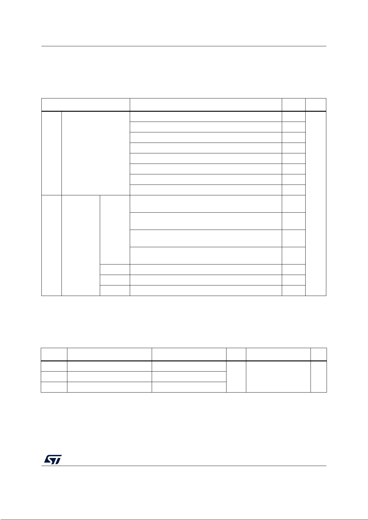
STM32WB15CC Electrical characteristics
6.3 Operating conditions
6.3.1 Summary of main performance
I
CORE
I
PERI
Table 20. Main performance at VDD = 3.3 V
Parameter Test conditions Typ Unit
Core current
consumption
VBAT (V
Standby (V
Shutdown (V
DD
= 1.8 V, VDD = 0 V) 0.001
BAT
= 1.8 V) 0.012
DD
= 1.8 V, 48 Kbytes RAM retention) 0.33
Sleep (16 MHz) 0.610
LP run (2 MHz) 190
Run (64 MHz) 4550
(1)
(2)
with Stop 1
(2)
with Stop 1
(2)
with Standby
(2)
with Standby
(1)
4500
5200
13
4
TBD
TBD
Peripheral
current
consumption
Radio RX
Radio TX 0 dBm output power
Advertising
(Tx = 0 dBm; period 1.28 s; 31 bytes, 3 channels)
Advertising
(Tx = 0 dBm, 6 bytes; period 10.24 s, 3 channels)
BLE
Advertising
(Tx = 0 dBm; period 1.28 s; 31 bytes, 3 channels)
Advertising
(Tx = 0 dBm, 6 bytes; period 10.24 s, 3 channels)
LP timers - 5.8
µA
LPUART - 8.1
RTC - 1.75
1. Power consumption including RF subsystem and digital processing.
2. Power consumption integrated over 100 s including Cortex-M4, RF subsystem, digital processing and Cortex M0+.
6.3.2 General operating conditions
Symbol Parameter Conditions Min Max Unit
f
HCLK
PCLK1
f
PCLK2
Internal AHB clock frequency -
Internal APB1 clock frequency -
Internal APB2 clock frequency -
Table 21. General operating conditions
064MHzf
DS13258 Rev 1 59/121
113

Electrical characteristics STM32WB15CC
Table 21. General operating conditions (continued)
Symbol Parameter Conditions Min Max Unit
V
Standard operating voltage -
DD
1.71
(1) (2)
ADC or COMP used 1.62
V
V
V
FBSMPS
V
DDRF
V
Analog supply voltage
DDA
Backup operating voltage - 1.55
BAT
ADC, COMP not used 0
SMPS feedback voltage - 1.4
Minimum RF voltage - 1.71
TT_xx I/O –0.3 V
I/O input voltage
IN
All I/O except TT_xx –0.3
DD
min (min (V
3.6 V, 5.5 V)
3.6
+ 0.3
DD
, V
DDA
(3)(4)
) +
Power dissipation at
P
T
D
= 85 °C for suffix 6 version, or
A
= 105 °C for suffix 7 version
T
A
Ambient temperature for
suffix 6 version
UFQFPN48 - 722 mW
Maximum power dissipation
Low-power dissipation
(5)
–40
85
105
TA
Ambient temperature for
suffix 7 version
Maximum power dissipation
Low-power dissipation
(5)
-40
Suffix 6 version
T
Junction temperature range
J
1. When RESET is released functionality is guaranteed down to V
2. When V
mode, or the SMPS is not enabled.
3. This formula has to be applied only on the power supplies related to the IO structure described by the pin definition table.
Maximum I/O input voltage is the smallest value between min (V
4. For operation with voltage higher than min (V
disabled.
5. In low-power dissipation state, T
Thermal characteristics).
is lower then 1.95 V, the SMPS operation mode is enabled by the BORH configuration to force SMPS bypass
DDmin
can be extended to this range as long as TJ does not exceed TJmax (see Section 7.2:
A
Suffix 7 version 125
Min.
BOR0
, V
) + 3.6 V and 5.5 V.
DDA
DD
DD
, V
) + 0.3 V, the internal pull-up and pull-down resistors must be
DDA
-40
105
125
105
V
°C
6.3.3 RF BLE characteristics
RF characteristics are given at 1 Mbps, unless otherwise specified.
Symbol Parameter Test conditions Min Typ Max Unit
F
F
xtal
Frequency operating range - 2402 - 2480
op
Crystal frequency
F Delta frequency
Rgfsk On air data rate
PLLres RF channel spacing
60/121 DS13258 Rev 1
Table 22. RF transmitter BLE characteristics
--32-
--250-
--12
--2-
MHz
kHz
Mbps
MHz

STM32WB15CC Electrical characteristics
Table 23. RF transmitter BLE characteristics (1 Mbps)
(1)
Symbol Parameter Test conditions Min Typ Max Unit
SMPS Bypass or ON
Maximum output power
P
rf
0 dBm output power
Minimum output power
P
band
Output power variation over the band
BWdB 6 dB signal bandwidth
IBSE In band spurious emission
f
d
Frequency drift
maxdr Maximum drift rate
fo Frequency offset
f1 Frequency deviation average
(V
VDD > 1.95 V)
SMPS Bypass or ON
(V
VDD > 1.71 V), Code 29
Tx = 0 dBm - Typical -0.5 - 0.4 dB
Tx = max output power - 670 - kHz
2 MHz Bluetooth
3 MHz Bluetooth
Bluetooth® Low Energy: ±50 kHz -50 - +50 kHz
Bluetooth
±20 kHz / 50 µs
Bluetooth
±150 kHz
Bluetooth
between 225 and 275 kHz
FBSMPS
FBSMPS
= 1.7 V and
(2)
= 1.4 V and
(2)
-5.5-
-3.6-
--0-
---20-
®
Low Energy:-20 dBm - -50 -
®
Low Energy: -30 dBm - -53 -
®
Low Energy:
®
Low Energy:
®
Low Energy:
-20 - +20
-150 - +150
225 - 275
dBm
dBm
kHz/
50 µs
kHz
fa
OBSE
1. Measured in conducted mode, based on reference design (see AN5165), using output power specific external RF filter and
impedance matching networks to interface with a 50 antenna.
2. V
SMPS on STM32WB Series microcontrollers, available on www.st.com).
3. Suitable for systems targeting compliance with worldwide radio-frequency regulations ETSI EN 300 328 and EN 300 440
Class 2 (Europe), FCC CFR47 Part 15 (US), and ARIB STD-T66 (Japan).
Frequency deviation
f2 (average) / f1 (average)
Out of band
(3)
spurious emission
and VDD must be set to different voltage levels, depending upon the desired TX signal (see AN5246 Usage of
FBSMPS
Table 24. RF transmitter BLE characteristics (2 Mbps)
< 1 GHz - - -62 -
1 GHz - - -45 -
Bluetooth® Low Energy:> 0.80 0.80 - - -
dBm
(1)
Symbol Parameter Test conditions Min Typ Max Unit
SMPS Bypass or ON
(V
VDD > 1.95 V)
Maximum output power
P
rf
SMPS Bypass or ON
(V
VDD > 1.71 V), Code 29
0 dBm output power
Minimum output power
FBSMPS
FBSMPS
= 1.7 V and
(2)
= 1.4 V and
(2)
-5.5-
-3.6-
--0-
---20-
dBm
DS13258 Rev 1 61/121
113
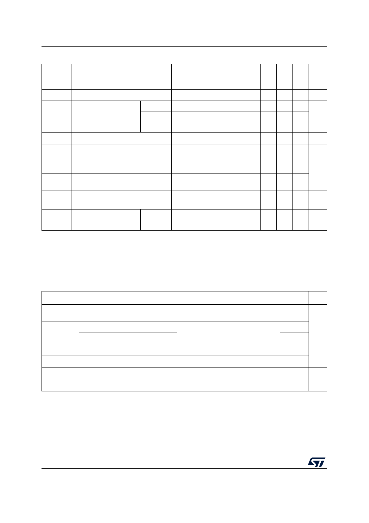
Electrical characteristics STM32WB15CC
Table 24. RF transmitter BLE characteristics (2 Mbps)
(1)
(continued)
Symbol Parameter Test conditions Min Typ Max Unit
P
band
Output power variation over the band
BW6dB 6 dB signal bandwidth
4 MHz Bluetooth
IBSE In band spurious emission
6 MHz Bluetooth
f
d
Frequency drift
maxdr Maximum drift rate
fo Frequency offset
f1 Frequency deviation average
fa
OBSE
1. Measured in conducted mode, based on reference design (see AN5165), using output power specific external RF filter and
impedance matching networks to interface with a 50 antenna.
2. V
FBSMPS
SMPS on STM32WB Series microcontrollers, available on www.st.com).
3. Suitable for systems targeting compliance with worldwide radio-frequency regulations ETSI EN 300 328 and EN 300 440
Class 2 (Europe), FCC CFR47 Part 15 (US), and ARIB STD-T66 (Japan).
Frequency deviation
f2 (average) / f1 (average)
Out of band
(3)
spurious emission
and VDD must be set to different voltage levels, depending upon the desired TX signal (see AN5246 Usage of
< 1 GHz - - -62 -
1 GHz - - -45 -
Tx = 0 dBm - Typical -0.5 - 0.4 dB
Tx = maximum output power - 670 - kHz
®
Low Energy: -20 dBm - -55 -
®
Low Energy: -20 dBm - -55 -
®
Low Energy: -30 dBm -56
dBm5 MHz Bluetooth
Bluetooth® Low Energy: ±50 kHz -50 - 50 kHz
Bluetooth
±20 kHz / 50 µs
Bluetooth
Bluetooth
between 450 and 550 kHz
®
Low Energy:
®
Low Energy: ±150 kHz -150 - 150
®
Low Energy:
-20 - 20
450 - 550
kHz/
50 µs
Bluetooth® Low Energy:> 0.80 0.80 - - -
dBm
kHz
Table 25. RF receiver BLE characteristics (1 Mbps)
Symbol Parameter Test conditions Typ Unit
Prx_max Maximum input signal
High sensitivity mode (SMPS Bypass)
(1)
Psens
Rssi
Rssi
Rssi
maxrange
minrange
accu
C/Ico
High sensitivity mode (SMPS ON) -95
RSSI maximum value - -7
RSSI minimum value - -94
RSSI accuracy - 2
Co-channel rejection Bluetooth
PER <30.8%
Bluetooth
®
Low Energy: min -10 dBm
PER <30.8%
Bluetooth® Low Energy: max -70 dBm
®
Low Energy: 21 dB 9
-4
-95.5
dBm
dB
62/121 DS13258 Rev 1

STM32WB15CC Electrical characteristics
Table 25. RF receiver BLE characteristics (1 Mbps) (continued)
Symbol Parameter Test conditions Typ Unit
C/I
Adjacent channel interference
C/Image Image rejection (F
Adj 5 MHz
Bluetooth
Adj -5 MHz
Bluetooth
Adj = 4 MHz
Bluetooth
Adj = -4 MHz
Bluetooth
Adj = 3 MHz
Bluetooth
Adj = 2 MHz
Bluetooth
Adj = -2 MHz
Bluetooth
Adj = 1 MHz
Bluetooth
Adj = -1 MHz
Bluetooth
= -3 MHz) Bluetooth® Low Energy: -9 dB -28
image
|f2-f1| = 3 MHz
Bluetooth
®
Low Energy: -27 dB
®
Low Energy:-27 dB
®
Low Energy:-27 dB
®
Low Energy:-15 dB
®
Low Energy:-27 dB
®
Low Energy:-17 dB
®
Low Energy:-15 dB
®
Low Energy: 15 dB
®
Low Energy: 15 dB
®
Low Energy: -50 dBm
-46
-48
-46
-33
-46
dB
-39
-35
-2
2
-36
P_IMD Intermodulation
P_OBB Out of band blocking
1. With ideal TX.
|f2-f1| = 4 MHz
Bluetooth
|f2-f1| = 5 MHz
Bluetooth
30 to 2000 MHz
Bluetooth
2003 to 2399 MHz
Bluetooth
2484 to 2997 MHz
Bluetooth
3 to 12.75 GHz
Bluetooth
®
Low Energy: -50 dBm
®
Low Energy:-50 dBm
®
Low Energy: -30 dBm
®
Low Energy: -35 dBm
®
Low Energy: -35 dBm
®
Low Energy: -30 dBm
-35
-33
-2
-8
-4
6
dBm
DS13258 Rev 1 63/121
113

Electrical characteristics STM32WB15CC
Table 26. RF receiver BLE characteristics (2 Mbps)
Symbol Parameter Test conditions Typ Unit
Prx_max Maximum input signal
High sensitivity mode (SMPS Bypass)
(1)
Psens
Rssi
Rssi
Rssi
maxrange
minrange
accu
C/Ico
C/I
High sensitivity mode (SMPS ON) -92.5
RSSI maximum value - -7
RSSI minimum value - -94
RSSI accuracy - 2
Co-channel rejection Bluetooth
Adjacent channel interference
PER <30.8%
Bluetooth
®
Low Energy: min -10 dBm
PER <30.8%
®
Bluetooth
Adj 8 MHz
Bluetooth
Adj -8 MHz
Bluetooth
Adj = 6 MHz
Bluetooth
Adj = -6 MHz
Bluetooth
Adj = 4 MHz
Bluetooth
Low Energy: max -70 dBm
®
Low Energy: 21 dB 10
®
Low Energy: -27 dB
®
Low Energy: -27 dB
®
Low Energy: -27 dB
®
Low Energy: -15 dB
®
Low Energy: -17 dB
-4
-92.5
-48
-44
-48
-46
-42
dBm
dB
dB
C/Image Image rejection (F
P_IMD Intermodulation
P_OBB Out of band blocking
1. With ideal TX.
Adj = 2 MHz
Bluetooth
Adj = -2 MHz
Bluetooth
= -3 MHz) Bluetooth® Low Energy: -9 dB -26
image
|f2-f1| = 6 MHz
Bluetooth
|f2-f1| = 8 MHz
Bluetooth
|f2-f1| = 10 MHz
Bluetooth
30 to 2000 MHz
Bluetooth
2003 to 2399 MHz
Bluetooth
2484 to 2997 MHz
Bluetooth
3 to 12.75 GHz
Bluetooth
®
Low Energy: 15 dB
®
Low Energy: 15 dB
®
Low Energy: -50 dBm
®
Low Energy: -50 dBm
®
Low Energy:-50 dBm
®
Low Energy: -30 dBm
®
Low Energy: -35 dBm
®
Low Energy: -35 dBm
®
Low Energy: -30 dBm
-3
-3
-28
-31
-30
-3
-12
-7
3
dBm
64/121 DS13258 Rev 1

STM32WB15CC Electrical characteristics
Table 27. RF BLE power consumption for V
Symbol Parameter Typ Unit
TX maximum output power consumption (SMPS Bypass) 12.5
I
txmax
TX maximum output power consumption (SMPS On, V
TX 0 dBm output power consumption (SMPS Bypass) 8.7
I
tx0dbm
TX 0 dBm output power consumption (SMPS On, V
FBSMPS
Rx consumption (SMPS Bypass) 7.7
I
rxlo
1. Power consumption including RF subsystem and digital processing.
Rx consumption (SMPS On, V
= 1.4 V) 4.5
FBSMPS
6.3.4 Operating conditions at power-up / power-down
The parameters given in Tab le 28 are derived from tests performed under the ambient
temperature condition summarized in Tab le 21.
Symbol Parameter Conditions Min Max Unit
t
VDD
t
VDDA
t
VDDRF
Table 28. Operating conditions at power-up / power-down
VDD rise time rate
fall time rate 10
V
DD
V
rise time rate
DDA
fall time rate 10
V
DDA
V
rise time rate
DDRF
fall time rate -
V
DDRF
-
-
-
DD
FBSMPS
= 3.3 V
(1)
= 1.7 V) 7.8
= 1.4 V) 5.2
-
0
-
mA
µs/V
DS13258 Rev 1 65/121
113

Electrical characteristics STM32WB15CC
6.3.5 Embedded reset and power control block characteristics
The parameters given in Tab le 29 are derived from tests performed under the ambient
temperature conditions summarized in Table 21: General operating conditions.
Table 29. Embedded reset and power control block characteristics
Symbol Parameter Conditions
t
RSTTEMPO
V
BOR0
(2)
Reset temporization after BOR0 is detected V
Brown-out reset threshold 0
rising - 250 400 s
DD
Rising edge 1.62 1.66 1.70
Falling edge 1.60 1.64 1.69
(2)
Rising edge 2.06 2.10 2.14
V
BOR1
Brown-out reset threshold 1
Falling edge 1.96 2.00 2.04
Rising edge 2.26 2.31 2.35
V
BOR2
Brown-out reset threshold 2
Falling edge 2.16 2.20 2.24
(1)
Min Typ Max Unit
V
BOR3
V
BOR4
V
PVD0
V
PVD1
V
PVD2
V
PVD3
V
PVD4
V
PVD5
V
PVD6
V
hyst_BORH0
V
hyst_BOR_PVD
(BOR_PVD)
I
DD
Brown-out reset threshold 3
Brown-out reset threshold 4
Programmable voltage detector threshold 0
PVD threshold 1
PVD threshold 2
PVD threshold 3
PVD threshold 4
PVD threshold 5
PVD threshold 6
Hysteresis voltage of BORH0
Hysteresis voltage of BORH (except
BORH0) and PVD
(3)
BOR
(2)
(except BOR0) and PVD
consumption from V
DD
Rising edge 2.56 2.61 2.66
Falling edge 2.47 2.52 2.57
Rising edge 2.85 2.90 2.95
Falling edge 2.76 2.81 2.86
Rising edge 2.10 2.15 2.19
Falling edge 2.00 2.05 2.10
Rising edge 2.26 2.31 2.36
Falling edge 2.15 2.20 2.25
Rising edge 2.41 2.46 2.51
Falling edge 2.31 2.36 2.41
Rising edge 2.56 2.61 2.66
Falling edge 2.47 2.52 2.57
Rising edge 2.69 2.74 2.79
Falling edge 2.59 2.64 2.69
Rising edge 2.85 2.91 2.96
Falling edge 2.75 2.81 2.86
Rising edge 2.92 2.98 3.04
Falling edge 2.84 2.90 2.96
Hysteresis in
continuous mode
Hysteresis in
other mode
-20-
-30-
- - 100 -
- - 1.1 1.6 µA
V
V
mV
66/121 DS13258 Rev 1

STM32WB15CC Electrical characteristics
Table 29. Embedded reset and power control block characteristics (continued)
Symbol Parameter Conditions
(1)
Min Typ Max Unit
V
PVM3
V
hyst_PVM3
(PVM3)
I
DD
1. Continuous mode means Run/Sleep modes, or temperature sensor enable in Low-power run/Low-power sleep modes.
2. Guaranteed by design.
3. BOR0 is enabled in all modes (except Shutdown) and its consumption is therefore included in the supply current
characteristics tables.
V
peripheral voltage monitoring
DDA
Falling edge 1.6 1.64 1.68
PVM3 hysteresis - - 10 - mV
(2)
PVM3 consumption from V
DD
--2-µA
6.3.6 Embedded voltage reference
The parameters in Tabl e 30 are derived from tests performed under the ambient
temperature and supply voltage conditions summarized in Table 21: General operating
conditions.
Rising edge 1.61 1.65 1.69
Symbol Parameter Conditions Min Typ Max Unit
Internal reference voltage –40 °C < TJ < +125 °C 1.182 1.212 1.232 V
ADC sampling time when reading
(1)
the internal reference voltage
Start time of reference voltage
buffer when ADC is enable
V
REFINT
)
VDD when converted by ADC
t
S_vrefint
t
start_vrefint
IDD(V
V
REFINT
REFINTBUF
Table 30. Embedded internal voltage reference
-4
--812
buffer consumption from
- - 12.5 20
(2)
--
(2)
(2)
V
µs
µA
V
REFINT
T
Coeff
A
Coeff
V
DDCoeff
V
REFINT_DIV1
V
REFINT_DIV2
V
REFINT_DIV3
1. The shortest sampling time can be determined in the application by multiple iterations.
2. Guaranteed by design.
Internal reference voltage spread
over the temperature range
Temperature coefficient –40 °C < TJ < +125 °C - 30 50
Long term stability 1000 hours, TJ = 25 °C - 300 1000
Voltage coefficient 3.0 V < VDD < 3.6 V - 250 1200
1/4 reference voltage
1/2 reference voltage 49 50 51
3/4 reference voltage 74 75 76
= 3 V - 5 7.5
V
DD
-
DS13258 Rev 1 67/121
24 25 26
(2)
(2)
(2)
(2)
mV
ppm/°C
ppm
ppm/V
%
V
REFINT
113

Electrical characteristics STM32WB15CC
MSv40169V1
1.185
1.19
1.195
1.2
1.205
1.21
1.215
1.22
1.225
1.23
1.235
-40 -20 0 20 40 60 80 100 120
V
°C
Mean Min Max
Figure 14. V
6.3.7 Supply current characteristics
The current consumption is a function of several parameters and factors such as the
operating voltage, ambient temperature, I/O pin loading, device software configuration,
operating frequencies, I/O pin switching rate, program location in memory and executed
binary code.
vs. temperature
REFINT
The current consumption is measured as described in Figure 13: Current consumption
measurement scheme.
Typical and maximum current consumption
The MCU is put under the following conditions:
All I/O pins are in analog input mode
All peripherals are disabled except when explicitly mentioned
The Flash memory access time is adjusted with the minimum wait states number,
depending on the f
to CPU clock (HCLK) frequency” available in the RM0473 reference manual).
When the peripherals are enabled f
For Flash memory and shared peripherals f
The parameters given in Tab le 31 to Ta bl e 41 are derived from tests performed under
ambient temperature and supply voltage conditions summarized in Tab le 21: General
operating conditions.
frequency (refer to the table “Number of wait states according
HCLK
= f
PCLK
HCLK
PCLK
= f
HCLK
= f
HCLKS
68/121 DS13258 Rev 1

DS13258 Rev 1 69/121
Table 31. Current consumption in Run and Low-power run modes, code with data processing
running from Flash memory, ART enable (Cache ON Prefetch OFF), V
Conditions Typ Max
Symbol Parameter
-f
f
I
DD
(Run)
Supply
current in
Run mode
= f
HCLK
16 MHz included,
= f
f
HCLK
f
HSI16
above 32 MHz
All peripherals disabled
up to
HSI16
= 32 MHz
HSE
+ PLL ON
-
SMPS
Supply
I
DD
(LPRun)
current in
Low-power
All peripherals disabled
f
HCLK
= f
MSI
run mode
1. Guaranteed by characterization results (mean ± 4 ), unless otherwise specified.
HCLK
64 MHz 6.35 6.40 6.45 6.50 7.25 7.37 7.57
32 MHz 3.25 3.30 3.35 3.40 3.29 3.53 3.78
16 MHz 1.75 1.75 1.80 1.85 2.06 2.18 2.46
64 MHz 4.55 4.55 4.60 4.60 - - -
32 MHz 2.90 2.90 2.95 3.00 - - -
16 MHz 2.15 2.15 2.15 2.20 - - -
2 MHz 0.190 0.205 0.235 0.285 0.270 0.460 0.630
1 MHz 0.105 0.115 0.145 0.195 0.170 0.320 0.490
400 kHz 0.0605 0.0905 0.140 0.008 0.230 0.390 0.390
100 kHz 0.024 0.034 0.0645 0.110 0.040 0.190 0.330
= 3.3 V
DD
(1)
25 °C 55 °C 85 °C 105 °C 25 °C 85 °C 105 °C
STM32WB15CC Electrical characteristics
Unit
mA

70/121 DS13258 Rev 1
Table 32. Current consumption in Run and Low-power run modes, code with data processing
running from SRAM1, V
Conditions Typ Max
Symbol Parameter
-f
f
I
DD
(Run)
Supply
current in
Run mode
= f
HCLK
16 MHz included,
= f
f
HCLK
f
+ PLL ON above
HSI16
32 MHz
All peripherals disabled
HSI16
= 32 MHz
HSE
up to
-
SMPS
Supply
I
DD
(LPRun)
current in
Low-power
= f
f
HCLK
MSI
All peripherals disabled
run mode
1. Guaranteed by characterization results (mean ± 4 ), unless otherwise specified.
HCLK
64 MHz 6.75 6.80 6.85 6.85 8.05 8.22 8.41
32 MHz 3.45 3.50 3.55 3.60 3.55 3.69 4.13
16 MHz 1.85 1.85 1.90 1.90 1.77 1.94 2.26
64 MHz 4.75 4.75 4.75 4.80 - - -
32 MHz 3.00 3.00 3.05 3.10 - - -
16 MHz 2.20 2.20 2.25 2.25 - - -
2 MHz 0.200 0.215 0.245 0.290 0.330 0.600 0.850
1 MHz 0.110 0.120 0.150 0.195 0.240 0.420 0.670
400 kHz 0.0525 0.0615 0.0905 0.135 0.160 0.310 0.520
100 kHz 0.024 0.034 0.0625 0.110 0.130 0.180 0.450
= 3.3 V
DD
(1)
25 °C 55 °C 85 °C 105 °C 25 °C 85 °C 105 °C
Electrical characteristics STM32WB15CC
Unit
mA

STM32WB15CC Electrical characteristics
Table 33. Typical current consumption in Run and Low-power run modes, with different codes
Symbol Parameter Conditions Code
running from Flash memory, ART enable (Cache ON Prefetch OFF)
TYP
, V
Unit
= 3.3 V
DD
TYP
Unit
25 °C 25 °C
Reduced code
6.35
99
(1)
Coremark 6.20 97
f
HCLK
= 64 MHz
Dhrystone 2.1 6.75 105
Fibonacci 6.05 95
While(1) 5.85 91
(1)
4.55 71
mA
µA/MHz
I
DD
(Run)
Supply current
in Run mode
+ PLL ON above 32 MHz
HSI16
SMPS ON,
= 64 MHz
f
HCLK
Reduced code
Coremark 4.45 70
Dhrystone 2.1 4.75 74
Fibonacci 4.40 69
All peripherals disabled
While(1) 4.30 67
Reduced code
(1)
2.27 35
up to 16 MHz included, f
SMPS ON,
f
HSI16
HCLK
Tx level = 0 dBm
= f
HCLK
f
= 64 MHz, RF
Coremark 2.22 34
Dhrystone 2.1 2.37 34
(2)
Fibonacci 2.19 34
While(1) 2.14 33
Reduced code
Coremark 190 95
Dhrystone 2.1 215 108
Fibonacci 185 93
I
DD
(LPRun)
Supply current
in
Low-power run
= f
f
HCLK
MSI
= 2 MHz
All peripherals disabled
While(1) 175 88
1. Reduced code used for characterization results provided in Table 31 and Table 32.
2. Value computed. MCU consumption when RF TX and SMPS are ON.
(1)
190
µA
95
µA/MHz
DS13258 Rev 1 71/121
113

Electrical characteristics STM32WB15CC
Table 34. Typical current consumption in Run and Low-power run modes,
with different codes running from SRAM1
Symbol Parameter Conditions Code
Reduced code
Coremark 6.30 98
f
HCLK
+ PLL ON above 32 MHz
= 64 MHz
Dhrystone 2.1 6.20 97
Fibonacci 6.05 95
While(1) 6.20 98
Reduced code
, V
= 3.3 V
DD
TYP
25 °C 25 °C
(1)
6.75
(1)
4.75 74
Unit
TYP
Unit
105
Coremark 4.50 70
Dhrystone 2.1 4.50 70
IDD(Run)
Supply current
in Run mode
HSI16
SMPS ON,
= 64 MHz
f
HCLK
Fibonacci 4.40 69
All peripherals disabled
While(1) 4.50 70
Reduced code
up to 16 MHz included, f
SMPS ON,
f
HCLK
HSI16
Tx level = 0 dBm
= f
HCLK
f
= 64 MHz, RF
Coremark 2.24 35
Dhrystone 2.1 2.24 35
(2)
Fibonacci 2.19 34
While(1) 2.24 35
Reduced code
Coremark 190 95
Dhrystone 2.1 185 93
Fibonacci 180 90
(LPRun)
I
DD
Supply current
in
Low-power run
= f
f
HCLK
MSI
= 2 MHz
All peripherals disabled
While(1) 185 93
1. Reduced code used for characterization results provided in Table 31 and Table 32.
2. Value computed. MCU consumption when RF TX and SMPS are ON.
(1)
2.37 37
(1)
200
mA
µA
µA/MHz
100
µA/MHz
72/121 DS13258 Rev 1

DS13258 Rev 1 73/121
Table 35. Current consumption in Sleep and Low-power sleep modes, Flash memory ON
Conditions TYP MAX
Symbol Parameter
All peripherals disabled f
HCLK
64 MHz 1.80 1.85 1.85 1.90 2.04 2.20 2.48
-
32 MHz 0.990 1.00 1.05 1.10 0.980 1.22 1.52
16 MHz 0.605 0.610 0.640 0.685 0.690 0.910 1.15
64 MHz 2.30 2.30 2.30 2.35 - - -
32 MHz 1.80 1.80 1.80 1.85 - - -
I
DD
(Sleep)
Supply
current in
Sleep mode,
= f
f
HCLK
HSI16
included,
= f
f
HCLK
f
HSI16
HSE
+ PLL ON above
32 MHz
up to 16 MHz
up to 32 MHz
SMPS
16 MHz 1.60 1.60 1.60 1.65 - - -
2 MHz 0.055 0.065 0.095 0.145 0.080 0.240 0.400
Supply
I
DD
(LPSleep)
current in
Low-power
sleep mode
f
HCLK
= f
MSI
1 MHz 0.036 0.047 0.0765 0.125 0.060 0.210 0.360
400 kHz 0.022 0.033 0.0625 0.110 0.030 0.180 0.320
100 kHz 0.016 0.0265 0.057 0.105 0.030 0.170 0.320
1. Guaranteed by characterization results (mean ± 4 ), unless otherwise specified.
STM32WB15CC Electrical characteristics
(1)
Unit
25 °C 55 °C 85 °C 105 °C 25 °C 85 °C 105 °C
mA
Table 36. Current consumption in Low-power sleep modes, Flash memory in Power down
Conditions TYP MAX
Symbol Parameter
All peripherals disabled f
Supply
I
DD
(LPSleep)
current in
low-power
f
HCLK
= f
MSI
sleep mode
1. Guaranteed by characterization results (mean ± 4 ), unless otherwise specified.
HCLK
2 MHz 55 66 96 145 79 291 520
1 MHz 37 47 77 125 62 252 480
400 kHz 22 33 63 110 36 225 436
100 kHz 17 27 57 105 34 219 432
(1)
Unit
25 °C 55 °C 85 °C 105 °C 25 °C 85 °C 105 °C
µA

74/121 DS13258 Rev 1
Conditions TYP MAX
Table 37. Current consumption in Stop 1 mode
(1)
Symbol Parameter
-V
0 °C 25 °C 40 °C 55 °C 85 °C 105 °C 0 °C 25 °C 85 °C 105 °C
DD
1.8 V 1.90 3.05 7.35 9.95 31.5 64.0 2.6 9.4 112.8 225.1
I
DD
(Stop 1)
Supply current
in Stop 1 mode,
RTC disabled
BLE disabled
2.4 V 1.85 3.05 5.50 10.0 31.0 64.5 - - - -
3.0 V 1.85 3.05 5.55 10.0 31.5 65.5 2.5 9.3 112.6 227.3
3.6 V 1.90 3.10 5.65 10.0 32.0 67.0 2.6 9.4 115.2 233.5
1.8 V 2.15 3.35 7.55 10.5 31.5 64.5 3.0 10.6 112.2 221.8
2.4 V 2.20 3.45 5.85 10.5 31.5 65.0 - - - -
3.0 V 2.30 3.50 6.00 10.5 32.0 66.0 3.1 10.9 114.0 229.0
3.6 V 2.45 3.65 6.25 11.0 32.5 67.5 3.4 10.9 115.4 230.5
1.8 V 2.00 3.35 7.85 10.5 31.5 64.5 2.2 10.1 112.3 221.6
2.4 V 2.05 3.45 5.90 10.5 31.5 65.0 - - - -
(2)
in
3.0 V 2.25 3.60 6.05 10.5 32.0 66.0 2.9 10.7 113.8 228.3
I
DD
(Stop 1
with
RTC)
Supply current
in Stop 1 mode,
RTC enabled,
BLE disabled
RTC clocked
by LSI
RTC clocked by
LSE quartz
Low drive mode
3.6 V 2.40 3.75 6.30 11.0 32.5 67.5 3.1 11.0 114.6 230.1
I
Supply current
DD
(wakeup
from
Stop1)
1. Guaranteed based on test during characterization (mean ± 4 ), unless otherwise specified.
2. Based on characterization done with a 32.768 kHz crystal (MC306-G-06Q-32.768, manufacturer JFVNY) with two 6.8 pF loading capacitors.
3. Wakeup with code execution from Flash memory. Average value given for a typical wakeup time as specified in Table 44: Low-power mode wakeup
during wakeup
from Stop 1
bypass mode
timings.
Wakeup clock
HSI16. See
Wakeup clock
MSI = 32 MHz.
See
(3)
(3)
.
3.0 V
.
-TBD--------
-TBD--------
Electrical characteristics STM32WB15CC
Unit
µA

DS13258 Rev 1 75/121
Conditions TYP MAX
Table 38. Current consumption in Stop 0 mode
(1)
Symbol Parameter
-V
0 °C 25 °C 40 °C 55 °C 85 °C 105 °C 0 °C 25 °C 85 °C 105 °C
DD
1.8 V 97.5 100 105 110 140 180 112.3 114.2 328.9 499.9
Supply current
in Stop 0 mode,
RTC disabled,
--
BLE disabled
I
DD
(Stop 0)
Supply current
during wakeup
from Stop 0
Bypass mode
1. Guaranteed based on test during characterization (mean ± 4 ), unless otherwise specified.
2. Wakeup with code execution from Flash memory. Average value given for a typical wakeup time as specified in Table 44: Low-power mode wakeup
timings.
Wakeup clock
HSI16. See
Wakeup clock
MSI = 32 MHz.
See
(2)
2.4 V 99.5 100 105 115 140 180 - - - -
3.0 V 100 105 110 115 140 180 119.1 134.3 331.5 495.0
3.6 V 100 105 110 115 145 185 165.0 135.7 358.2 511.1
(2)
.
-TBD--------
3.0 V
-TBD--------
.
STM32WB15CC Electrical characteristics
Unit
µA
Symbol Parameter
Supply current
in Standby
I
DD
(Standby)
mode (backup
registers and
SRAMs
retained),
RTC disabled
Table 39. Current consumption in Standby mode
Conditions TYP MAX
-VDD0 °C 25 °C 40 °C 55 °C 85 °C 105 °C 0 °C 25 °C 85 °C 105 °C
BLE disabled
No
independent
watchdog
BLE disabled
with
independent
watchdog
1.8 V
2.4 V
3.0 V
3.6 V
1.8 V
2.4 V
3.0 V
3.6 V
235 335 507 900 2900 6200 261 867 6599 14593
250 345 540 935 3000 6550 - - - -
255 355 565 985 3150 6950 334 907 6959 15509
280 390 625 1050 3400 7600 373 989 7270 16213
415 515 677 1100 3100 6350 814 1074 24 14741
465 565 765 1150 3200 6750 - - - -
520 625 840 1250 3400 7250 1309 1169 7188 15832
595 715 950 1400 3750 7900 1716 1259 7630 16403
(1)
Unit
A
n

76/121 DS13258 Rev 1
Table 39. Current consumption in Standby mode (continued)
Symbol Parameter
Conditions TYP MAX
-VDD0 °C 25 °C 40 °C 55 °C 85 °C 105 °C 0 °C 25 °C 85 °C 105 °C
RTC clocked
by LSI, no
independent
Supply current
watchdog
in Standby
I
DD
(Standby
with RTC)
mode (backup
registers and
SRAMs
retained),
RTC clocked
by LSI, with
independent
watchdog
RTC enabled
BLE disabled
RTC clocked
by LSE
(2)
quartz
in low
drive mode
Supply current
to be
I
DD
(SRAM)
subtracted in
(3)
Standby mode
-
when SRAM
is not retained
I
DD
(wakeup
from
Standby)
1. Guaranteed based on test during characterization (mean ± 4 ), unless otherwise specified.
2. Based on characterization done with a 32.768 kHz crystal (MC306-G-06Q-32.768, manufacturer JFVNY) with two 6.8 pF loading capacitors.
3. The supply current in Standby with SRAMs mode is: I
+ RTC) + IDD(SRAM).
4. Wakeup with code execution from Flash memory. Average value given for a typical wakeup time as specified in Table 44.
Supply current
during wakeup
from Standby
mode
Wakeup clock
is HSI16.
(4)
See
1.8 V
2.4 V
3.0 V
3.6 V
1.8 V
2.4 V
3.0 V
3.6 V
1.8 V
2.4 V
3.0 V
3.6 V
1.8 V
2.4 V 85.0 100 145 240 850 2050 - - - -
3.0 V
3.6 V
3.0 V
515 610 791 1200 3150 6450 700 1184 6933 15007
600 700 900 1300 3350 6900 - - - -
700 800 1000 1450 3600 7400 898 1419 8182 16026
815 935 1150 1600 3950 8100 995 1569 604 16995
550 650 830 1200 3200 6500 715 1187 6986 14984
650 750 950 1350 3400 6950 - - - -
765 865 1100 1500 3650 7500 1085 1487 7358 16358
905 1000 1250 1700 4050 8200 1190 1641 8042 17295
545 655 920 1250 3250 6550 623 1112 6958 14936
645 755 955 1350 3400 7000 - - - -
760 875 1100 1500 3700 7550 588 1094 7332 16285
920 1050 1300 1750 4100 8300 738 1171 7757 17377
79.0 92.0 130 215 730 1750 - - - -
95.0 110 165 285 1000 2450 - - - -
115 150 220 370 1250 3000 - - - -
-TBD--------
(Standby) + IDD(SRAMs). The supply current in Standby with RTC with SRAM mode is: IDD(Standby
DD
(1)
Electrical characteristics STM32WB15CC
Unit
nA
nA
mA

DS13258 Rev 1 77/121
Conditions TYP MAX
Table 40. Current consumption in Shutdown mode
(1)
Symbol Parameter
-V
Supply current
in Shutdown
I
DD
(Shutdown)
mode (backup
registers
-
retained) RTC
disabled
Supply current
I
DD
(Shutdown
with RTC)
in Shutdown
mode (backup
registers
retained) RTC
enabled
1. Guaranteed based on test during characterization (mean ± 4 ), unless otherwise specified.
2. Based on characterization done with a 32.768 kHz crystal (MC306-G-06Q-32.768, manufacturer JFVNY) with two 6.8 pF loading capacitors.
RTC clocked
by LSE
(2)
quartz
low drive
mode
1.8 V
2.4 V
3.0 V
3.6 V
1.8 V
2.4 V
in
3.0 V
3.6 V
Table 41. Current consumption in VBAT mode
Conditions TYP MAX
0 °C 25 °C 40 °C 55 °C 85 °C 105 °C 0 °C 25 °C 85 °C 105 °C
DD
5.00 12.0 31.0 74.0 365 990 - - 1207 3148
10.0 18.0 41.0 93.0 440 1200 - - - -
16.0 28.0 58.0 125 560 1500 - 140 1495 3874
34.0 54.0 99.0 190 745 1900 - 143 1788 4339
310 330 355 405 710 1350 - 2295 1948 3627
405 425 455 515 875 1650 - - - -
525 550 585 660 1100 2050 - 2310 2193 4635
680 710 760 860 1450 2600 - 2283 2704 5463
(1)
Symbol Parameter
-V
1.8 V
0 °C 25 °C 40 °C 55 °C 85 °C 105 °C 0 °C 25 °C 40 °C 55 °C 85 °C 105 °C
BAT
1.00 1.00 4.00 11.0 54.0 145 - - - - - -
STM32WB15CC Electrical characteristics
Unit
nA
Unit
RTC
disabled
Backup
I
domain
DD
(VBAT)
supply
current
RTC
enabled
and
clocked
by LSE
quartz
1. Guaranteed based on test during characterization (mean ± 4 ), unless otherwise specified.
2. Based on characterization done with a 32.768 kHz crystal (MC306-G-06Q-32.768, manufacturer JFVNY) with two 6.8 pF loading capacitors.
2.4 V 1.00 2.00 5.00 13.0 62.0 165 - - - - - -
3.0 V 1.00 3.00 8.00 19.0 88.0 245 - - - - - -
3.6 V 2.00 6.00 15.0 33.0 145 375 - - - - - -
1.8 V 200 210 220 235 290 385 - - - - - -
2.4 V 250 265 275 285 350 460 - - - - - -
3.0 V 315 330 340 360 440 605 - - - - - -
(2)
3.6 V 405 415 430 455 580 820 - - - - - -
nA

78/121 DS13258 Rev 1
Table 42. Current under Reset condition
TYP MAX
Symbol Conditions
0 °C 25 °C 40 °C 55 °C 85 °C 105 °C 0 °C 25 °C 40 °C 55 °C 85 °C 105 °C
1.8 V 310 315 320 330 365 420 - - - - - -
I
DD(RST)
2.4 V 330 335 345 350 385 445 - - - - - -
3.0 V 350 355 365 370 410 465 - 484 - - - -
3.6 V 370 375 385 390 430 485 - - - - - -
1. Guaranteed by characterization results, unless otherwise specified.
Electrical characteristics STM32WB15CC
(1)
Unit
µA

STM32WB15CC Electrical characteristics
I
SW
V
DDfSW
C=
I/O system current consumption
The current consumption of the I/O system has two components: static and dynamic.
I/O static current consumption
All the I/Os used as inputs with pull-up generate current consumption when the pin is
ex
ternally held low. The value of this current consumption can be simply computed by using
the pull-up/pull-down resistors values given in Ta bl e 64: I/O static characteristics.
For the output pins, any external pull-down or ext
estimate the current consumption.
Additional I/O current consumption is due to I/Os co
voltage level is externally applied. This current consumption is caused by the input Schmitt
trigger circuits used to discriminate the input value. Unless this specific configuration is
required by the application, this supply current consumption can be avoided by configuring
these I/Os in analog mode. This is notably the case of ADC input pins which should be
configured as analog inputs.
Caution: An
as a result of external electromagnetic noise. To avoid current consumption related to
floating pins, they must either be configured in analog mode, or forced internally to a definite
digital value. This can be done either by using pull-up/down resistors or by configuring the
pins in output mode.
I/O dynamic current consumption
In addition to the internal peripheral current consumption measured previously (see
Tab l e 43) the I/Os used by the application also contribute to the current consumption.
When an I/O pin switches, it uses the current f
pin circuitry and to charge/discharge the capacitive load (internal or external) connected to
the pin:
where
I
V
f
C is the total capacitance seen by the I/O pin: C = C
C
C
ernal load must also be considered to
nfigured as inputs if an intermediate
y floating input pin can also settle to an intermediate voltage level or switch inadvertently,
rom the I/O supply voltage to supply the I/O
is the current sunk by a switching I/O to charge/discharge the capacitive load
SW
is the I/O supply voltage
DD
is the I/O switching frequency
SW
+ C
I/O
EXT
is the I/O pin capacitance
I/O
is the PCB board capacitance plus any connected external device pin
EXT
capacitance.
The test pin is configured in push-pull output
frequency.
DS13258 Rev 1 79/121
mode and is toggled by software at a fixed
113

Electrical characteristics STM32WB15CC
On-chip peripheral current consumption
The current consumption of the on-chip peripherals is given in Tabl e 43. The MCU is placed
under the following conditions:
All I/O pins are in Analog mode
The given value is measured as the difference of the current consumptions when the
peripheral is clocked on and when it is clocked off
Ambient operating temperature and supply voltage conditions summarized in Table 17:
Voltage characteristics
The power consumption of the digital part of the on-chip peripherals is given in
Table 43. The power consumption of the analog part of the peripherals (where
applicable) is indicated in each related section of the datasheet.
Table 43. Peripheral current consumption
AHB1
(2)
AHB2
AHB Shared
Peripheral Run
Bus Matrix
TSC 0.940 0.900
CRC 0.400 0.380
DMA1 1.70 1.60
DMAMUX 1.90 1.80
All AHB1 peripherals 5.30 5.00
All AHB2 peripherals 1.70 1.70
TRNG independent clock domain 2.35 NA
TRNG clock domain 1.55 NA
SRAM2 1.35 1.25
FLASH 7.05 6.70
AES2 5.30 5.45
PKA 2.80 2.70
All AHB shared peripherals 14.5 15.5
(1)
2.10 1.70
Low-power
run and Sleep
Unit
µA/MHz
80/121 DS13258 Rev 1

STM32WB15CC Electrical characteristics
Table 43. Peripheral current consumption (continued)
APB1
APB2
Peripheral Run
RTCA 0.940 0.875
I2C1 independent clock domain 1.95 3.90
I2C1 clock domain 3.75 4.10
LPTIM1 independent clock domain 1.95 2.90
LPTIM1 clock domain 3.45 3.60
TIM2 4.55 4.00
LPTIM2 clock domain 3.45 3.70
LPTIM2 independent clock domain 1.95 2.90
WWDG 0.350 0.625
LPUART1 independent clock domain 2.60 3.70
LPUART1 clock domain 4.55 4.05
All APB1 peripherals 15.5 16.0
AHB to APB2
TIM1 6.25 6.10
USART1 independent clock domain 3.05 6.50
USART1 clock domain 6.25 5.50
SPI1 1.25 1.05
(3)
0.900 1.10
Low-power
run and Sleep
Unit
µA/MHz
ADC1 independent clock domain 0.940 0.600
ADC1 clock domain 0.780 0.600
All APB2 on 14.5 15.5
ALL 51.5 48.0
1. The BusMatrix is automatically active when at least one master is ON (CPU, DMA).
2. GPIOs consumption during read and write accesses.
3. The AHB to APB2 bridge is automatically active when at least one peripheral is ON on the APB2.
6.3.8 Wakeup time from Low-power modes and voltage scaling
transition times
The wakeup times given in Table 44 are the latency between the event and the execution of
the first user instruction.
The device goes in Low-power mode after the WFE (Wait For Event) instruction.
DS13258 Rev 1 81/121
113

Electrical characteristics STM32WB15CC
Table 44. Low-power mode wakeup timings
(1)
Symbol Parameter Conditions Typ Max Unit
Wakeup time from
t
WUSLEEP
Sleep mode
-TBDTBD
to Run mode
t
WULPSLEEP
t
WUSTOP0
Wakeup time from
Low-power sleep mode
to Low-power run mode
Wake up time from
Stop 0 mode
to Run mode in Flash
memory
Wake up time from
Wakeup in Flash with memory in power-down
during low-power sleep mode (FPDS = 1 in
PWR_CR1) and with clock MSI = 2 MHz
Wakeup clock MSI = 32 MHz TBD TBD
Wakeup clock HSI16 = 16 MHz TBD TBD
Wakeup clock MSI = 32 MHz TBD TBD
TBD TBD
Stop 0 mode
to Run mode in SRAM1
Wake up time from
-
Wakeup clock HSI16 = 16 MHz TBD TBD
Wakeup clock MSI = 32 MHz TBD TBD
Stop 1 mode
to Run in Flash memory
Wake up time from
Wakeup clock HSI16 = 16 MHz TBD TBD
Wakeup clock MSI = 32 MHz TBD TBD
Stop 1 mode
Wakeup clock HSI16 = 16 MHz TBD TBD
TBD TBD
Wakeup clock MSI = 4 MHz
TBD TBD
t
WUSTOP1
to Run in SRAM1
Wake up time from
Stop 1 mode to
Low-power run mode
in Flash memory
Wake up time from
Stop 1 mode to
Low-power run mode
Regulator in
Low-power
mode (LPR = 1
in PWR_CR1)
in SRAM1
Wakeup time from
t
WUSTBY
Standby mode
- Wakeup clock HSI16 = 16 MHz TBD TBD
to Run mode
1. Guaranteed by characterization results (VDD = 3 V, T = 25 °C).
No. of
CPU
cycles
µs
Table 45. Regulator modes transition times
(1)
Symbol Parameter Conditions Typ Max Unit
t
WULPRUN
1. Guaranteed by characterization results (VDD = 3 V, T = 25 °C).
2. Time until REGLPF flag is cleared in PWR_SR2.
Wakeup time from Low-power run mode to
Run mode
(2)
Code run with MSI 2 MHz TBD TBD µs
82/121 DS13258 Rev 1

STM32WB15CC Electrical characteristics
Table 46. Wakeup time using LPUART
(1)
Symbol Parameter Conditions Typ Max Unit
t
WULPPUART
LPUART baud rate allowing to wakeup up from Stop
mode when LPUART clock source is HSI16
1. Guaranteed by design.
Wakeup time needed to calculate the maximum
Stop mode 0 - TBD
Stop mode 1 - TBD
6.3.9 External clock source characteristics
High-speed external user clock generated from an external source
The high-speed external (HSE) clock is supplied with a 32 MHz crystal oscillator or a sine
wave.
The STM32WB15CC include internal programmable capacitances that can be used to tune
the crystal frequency in order to compensate the PCB parasitic one.
The characteristics in Tabl e 47 and Ta b le 49 are measured over recommended operating
conditions, unless otherwise specified. Typical values are referred to TA = 25 °C and
VDD = 3.0 V.
Table 47. HSE crystal requirements
Symbol Parameter Conditions Min Typ Max Unit
(1)
µs
f
NOM
Oscillator frequency - - 32 - MHz
Includes initial accuracy, stability over
f
TOL
Frequency tolerance
temperature, aging and frequency pulling
- - 50 ppm
due to incorrect load capacitance.
C
Load capacitance - 6 - 8 pF
L
ESR Equivalent series resistance - - - 100
1. 32 MHz XTAL is specified for two specific references: NX2016SA and NX1612SA.
Table 48. HSE clock source requirements
(1)
Symbol Parameter Conditions Min Typ Max Unit
f
HSE_ext
f
TOL
V
HSE
User external clock source frequency - 32 - MHz
Frequency tolerance
Clock input voltage limits Sine wave, AC-coupled
Includes initial accuracy, stability
over temperature and aging.
(2)
--50ppm
0.4 - 1.6 V
DuCy(HSE) Duty cycle - 45 50 55 %
1. Guaranteed by design.
2. Only AC coupled is supported (capacitor 470 pF to 100 nF).
PP
DS13258 Rev 1 83/121
113

Electrical characteristics STM32WB15CC
Table 49. HSE oscillator characteristics
Symbol Parameter Conditions Min Typ Max Unit
t
SUA(HSE)
Startup time
for 80% amplitude stabilization
V
stabilized, XOTUNE=000000,
DDRF
–40 to +125 °C range
- 1000 -
µs
t
SUR(HSE)
I
DDRF(HSE)
XOT
g(HSE)
XOT
fp(HSE)
XOT
nb(HSE)
XOT
st(HSE)
Startup time
for XOREADY signal
HSE current consumption HSEGMC=000, XOTUNE=000000 - 50 - µA
XOTUNE granularity
XOTUNE frequency pulling ±20 ±40 -
XOTUNE number of tuning bits - 6 - bit
XOTUNE setting time - - 0.1 ms
V
stabilized, XOTUNE=000000,
DDRF
–40 to +125 °C range
Capacitor bank
-250 -
-15
ppm
Offset = 10 kHz - - -127
(1)
n(HSE)
Phase noise for 32 MHz
dBc / HzOffset = 100 kHz - - -135
Offset = 1 MHz - - -138
1. Guaranteed only with a 32 MHz Xtal.
Note: For information about the trimming of the oscillator refer to AN5165 “Development of RF
hardware using STM32WB microcontrollers”, available on www.st.com.
Low-speed external user clock generated from an external source
The low-speed external (LSE) clock can be supplied with a 32.768 kHz crystal resonator
oscillator. The information provided in this section is based on design simulation results
obtained with typical external components specified in
resonator and the load capacitors have to be placed as close as possible to the oscillator
pins to minimize output distortion and startup stabilization time.
Refer to the crystal resonator manufacturer for more details on the resonator characteristics
(frequency, package, accuracy).
Symbol Parameter Conditions Min Typ Max Unit
I
DD(LSE)
LSE current consumption
Table 50. Low-speed external user clock characteristics
LSEDRV[1:0] = 00
Low drive capability
LSEDRV[1:0] = 01
Medium low drive capability
LSEDRV[1:0] = 10
Medium high drive capability
LSEDRV[1:0] = 11
High drive capability
Tabl e 50. In the application, the
(1)
-250-
-315-
-500-
-630-
nA
84/121 DS13258 Rev 1

STM32WB15CC Electrical characteristics
MS30253V2
OSC32_IN
OSC32_OUT
Drive
programmable
amplifier
f
LSE
32.768 kHz
resonator
Resonator with integrated
capacitors
C
L1
C
L2
Table 50. Low-speed external user clock characteristics
(1)
(continued)
Symbol Parameter Conditions Min Typ Max Unit
LSEDRV[1:0] = 00
Low drive capability
LSEDRV[1:0] = 01
Medium low drive capability
G
mcritmax
Maximum critical crystal g
m
LSEDRV[1:0] = 10
Medium high drive capability
LSEDRV[1:0] = 11
High drive capability
(2)
t
SU(LSE)
1. Guaranteed by design.
2. t
SU(LSE)
reached. This value is measured for a standard crystal and it can vary significantly with the crystal manufacturer.
Startup time VDD stabilized - 2 - s
is the startup time measured from the moment it is enabled (by software) until a stable 32 kHz oscillation is
- - 0.50
- - 0.75
µA / V
- - 1.70
- - 2.70
Note: For information on selecting the crystal refer to application note AN2867 “Oscillator design
guide for STM8S, STM8A and STM32 microcontrollers” available from www.st.com.
Figure 15. Typical application with a 32.768 kHz crystal
Note: No external resistors are required between OSC32_IN and OSC32_OUT, and it is forbidden
to add one.
In bypass mode the LSE oscillator is switched off and the input pin is a standard GPIO.
The external clock signal has to respect the I/O characteristics detailed in Section 6.3.16.
The recommend clock input waveform is shown in Figure 16.
DS13258 Rev 1 85/121
113

Electrical characteristics STM32WB15CC
MS19215V2
V
LSEH
t
f(LSE)
90%
10%
T
LSE
t
t
r(LSE)
V
LSEL
t
w(LSEH)
t
w(LSEL)
Figure 16. Low-speed external clock source AC timing diagram
Table 51. Low-speed external user clock characteristics
Symbol Parameter Conditions Min Typ Max Unit
f
LSE_ext
V
LSEH
V
LSEL
t
w(LSEH)
t
w(LSEL)
f
tolLSE
1. Guaranteed by design.
User external clock
source frequency
OSC32_IN input pin
high level voltage
OSC32_IN input pin
low level voltage
OSC32_IN high or
low time
Frequency
tolerance
Includes initial accuracy,
stability over temperature,
aging and frequency pulling
- 21.2 32.768 44.4 kHz
- 0.7 V
-V
- 250 - - ns
6.3.10 Internal clock source characteristics
The parameters given in Tab le 52 are derived from tests performed under ambient
temperature and supply voltage conditions summarized in Table 21: General operating
conditions. The provided curves are characterization results, not tested in production.
(1)
– Bypass mode
DDx
-V
DDx
V
SS
- 0.3 V
DDx
-500 - +500 ppm
High-speed internal (HSI16) RC oscillator
Symbol Parameter Conditions Min Typ Max Unit
f
HSI16
86/121 DS13258 Rev 1
HSI16 frequency V
Table 52. HSI16 oscillator characteristics
(1)
= 3.0 V, TA= 30 °C 15.88 - 16.08 MHz
DD

STM32WB15CC Electrical characteristics
MSv39299V1
15.6
15.7
15.8
15.9
16
16.1
16.2
16.3
16.4
MHz
min mean max
+1%
-1%
+2%
-2%
+1.5%
-1.5%
-40 -20 0 20 40 60 80 100 120 °C
Table 52. HSI16 oscillator characteristics
(1)
(continued)
Symbol Parameter Conditions Min Typ Max Unit
Trimming code
is not a multiple of 64
0.2 0.3 0.4
TRIM HSI16 user trimming step
(HSI16)
(HSI16)
(2)
(2)
Duty cycle - 45 - 55
HSI16 oscillator frequency drift
over temperature
HSI16 oscillator frequency drift
over V
DD
HSI16 oscillator start-up time - - 0.8 1.2
(2)
HSI16 oscillator stabilization time - - 3 5
(2)
HSI16 oscillator power consumption - - 155 190 A
DuCy(HSI16)
Te mp
VDD
tsu(HSI16)
(HSI16)
t
stab
(HSI16)
I
DD
1. Guaranteed by characterization results.
2. Guaranteed by design.
Trimming code
is a multiple of 64
= 0 to 85 °C -1 - 1
T
A
= –40 to 125 °C -2 - 1.5
T
A
VDD = 1.62 V to 3.6 V -0.1 - 0.05
-4 -6 -8
Figure 17. HSI16 frequency vs. temperature
%
s
DS13258 Rev 1 87/121
113

Electrical characteristics STM32WB15CC
Multi-speed internal (MSI) RC oscillator
Table 53. MSI oscillator characteristics
Symbol Parameter Conditions Min Typ Max Unit
Range 0 98.7 100 101.3
Range 1 197.4 200 202.6
Range 2 394.8 400 405.2
Range 3 789.6 800 810.4
Range 4 0.987 1 1.013
(1)
kHz
TEMP
f
MSI
(MSI)
MSI frequency
after factory
calibration, done
at V
DD
TA=30 °C
MSI oscillator
(2)
frequency drift
over temperature
=3 V and
MSI mode
PLL mode
XTAL=
32.768 kHz
MSI mode
Range 5 1.974 2 2.026
Range 6 3.948 4 4.052
Range 7 7.896 8 8.104
Range 8 15.79 16 16.21
Range 9 23.69 24 24.31
Range 10 31.58 32 32.42
Range 11 47.38 48 48.62
Range 0 - 98.304 -
Range 1 - 196.608 -
Range 2 - 393.216 -
Range 3 - 786.432 -
Range 4 - 1.016 -
Range 5 - 1.999 -
Range 6 - 3.998 -
Range 7 - 7.995 -
Range 8 - 15.991 -
Range 9 - 23.986 -
Range 10 - 32.014 -
Range 11 - 48.005 -
TA= 0 to 85 °C -3.5 - 3
= –40 to 125 °C -8 - 6
T
A
MHz
kHz
MHz
%
88/121 DS13258 Rev 1

STM32WB15CC Electrical characteristics
Table 53. MSI oscillator characteristics
(1)
(continued)
Symbol Parameter Conditions Min Typ Max Unit
VDD
(MSI)
MSI oscillator
frequency drift
(2)
over VDD
(reference is 3 V)
MSI mode
Range 0 to 3
Range 4 to 7
VDD =
1,62 to 3.6 V
V
=
DD
2.4 to 3.6 V
V
=
DD
1,62 to 3.6 V
=
V
DD
2.4 to 3.6 V
=
V
DD
1.62 to 3.6 V
-1.2 -
0.5
-0.5 -
-2.5 -
0.7
-0.8 -
-5 -
Range 8 to 11
V
=
F
SAMPLING
(2)(4)
(MSI)
CC jitter(MSI)
P jitter(MSI)
DD
2.4 to 3.6 V
Frequency
variation in
sampling mode
RMS cycle-to-
(4)
cycle jitter
(4)
RMS period jitter PLL mode Range 11 - - 50 -
(3)
PLL mode Range 11 - - 60 -
TA= –40 to 105 °C - 1 2
= –40 to 125 °C - 2 4
T
A
-1.6 -
%
1
ps
t
SU
t
STAB
(MSI)
(MSI)
MSI oscillator
(4)
start-up time
MSI oscillator
(4)
stabilization time
Range 0 - - 10 20
Range 1 - - 5 10
Range 2 - - 4 8
Range 3 - - 3 7
Range 4 to 7 - - 3 6
Range 8 to 11 - - 2.5 6
PLL mode
Range 11
10 % of final
frequency
5 % of final
frequency
1 % of final
frequency
- - 0.25 0.5
--0.51.25
---2.5
s
ms
DS13258 Rev 1 89/121
113

Electrical characteristics STM32WB15CC
Table 53. MSI oscillator characteristics
(1)
(continued)
Symbol Parameter Conditions Min Typ Max Unit
Range 0 - - 0.6 1
Range 1 - - 0.8 1.2
Range 2 - - 1.2 1.7
Range 3 - - 1.9 2.5
Range 4 - - 4.7 6
IDD(MSI)
(4)
MSI oscillator
power
consumption
MSI and
PLL mode
Range 5 - - 6.5 9
Range 6 - - 11 15
Range 7 - - 18.5 25
Range 8 - - 62 80
Range 9 - - 85 110
Range 10 - - 110 130
Range 11 - - 155 190
1. Guaranteed by characterization results.
2. This is a deviation for an individual part once the initial frequency has been measured.
3. Sampling mode means Low-power run/Low-power sleep modes with Temperature sensor disable.
4. Guaranteed by design.
µA
Figure 18. Typical current consumption vs. MSI frequency
90/121 DS13258 Rev 1

STM32WB15CC Electrical characteristics
Low-speed internal (LSI) RC oscillator
Table 54. LSI1 oscillator characteristics
Symbol Parameter Conditions Min Typ Max Unit
V
= 3.0 V, TA = 30 °C 31.04 - 32.96
f
LSI
t
(LSI1)
SU
(LSI1)
t
STAB
IDD(LSI1)
1. Guaranteed by characterization results.
2. Guaranteed by design.
LSI1 frequency
(2)
LSI1 oscillator start-up time - - 80 130
(2)
LSI1 oscillator stabilization time 5% of final frequency - 125 180
LSI1 oscillator power
(2)
consumption
DD
= 1.62 to 3.6 V, TA = -40 to 125 °C 29.5 - 34
V
DD
- - 110 180 nA
(1)
kHz
s
Table 55. LSI2 oscillator characteristics
(1)
Symbol Parameter Conditions Min Typ Max Unit
VDD = 3.0 V, TA = 30 °C TBD - TBD
= 1.62 to 3.6 V, TA = -40 to 125 °C TBD - TBD
V
DD
kHz
t
SU
I
DD
f
LSI2
(LSI2)
(LSI2)
Frequency
(3)
Start-up time - TBD - TBD ms
(3)
Power consumption - - TBD TBD nA
(2)
TEMP(LSI2) Stability over temperature - TBD - TBD ppm/ °C
1. Guaranteed by characterization results.
2. LSI2 cannot be trimmed.
3. Guaranteed by design.
6.3.11 PLL characteristics
The parameters given in Tab le 56 are derived from tests performed under temperature and
VDD supply voltage conditions summarized in Tab le 21: General operating conditions.
Table 56. PLL characteristics
Symbol Parameter Conditions Min Typ Max Unit
(2)
f
PLL_IN
f
PLL_P_OUT
f
PLL_Q_OUT
f
PLL_R_OUT
f
VCO_OUT
t
LOCK
PLL input clock
PLL input clock duty cycle - 45 - 55 %
PLL multiplier output clock P - 2 - 64
PLL multiplier output clock Q - 8 - 64
PLL multiplier output clock R - 8 - 64
PLL VCO output - 96 - 344
PLL lock time - - 15 40 s
RMS cycle-to-cycle jitter
Jitter
System clock 64 MHz
RMS period jitter - 30 -
(1)
-2.66-16MHz
MHz
-40ps
DS13258 Rev 1 91/121
113

Electrical characteristics STM32WB15CC
Table 56. PLL characteristics
(1)
(continued)
Symbol Parameter Conditions Min Typ Max Unit
VCO freq = 96 MHz - 200 260
IDD(PLL)
PLL power consumption
(1)
on V
DD
VCO freq = 344 MHz - 520 650
1. Guaranteed by design.
2. Take care of using the appropriate division factor M to obtain the specified PLL input clock values. The M factor is shared
between the two PLLs.
6.3.12 Flash memory characteristics
Table 57. Flash memory characteristics
Symbol Parameter Conditions Typ Max Unit
t
prog
t
prog_row
t
prog_page
t
ERASE
t
ME
64-bit programming time - 81.7 90.8 µs
One row (64 double word)
programming time
One page (2 Kbytes)
programming time
Normal programming 5.2 5.5
Fast programming 3.8 4.0
Normal programming 41.8 43.0
Fast programming 30.4 31.0
Page (2 Kbytes) erase time - 22.0 24.5
Mass erase time - 22.1 25.0
Write mode 3.4 -
I
DD
Average consumption from V
DD
Erase mode 3.4 -
(1)
ms
mA
AVCO freq = 192 MHz - 300 380
1. Guaranteed by design.
Table 58. Flash memory endurance and data retention
Symbol Parameter Conditions Min
N
END
t
RET
1. Guaranteed by characterization results.
2. Cycling performed over the whole temperature range.
Endurance TA = –40 to +105 °C 10 kcycles
1 kcycle
1 kcycle
1 kcycle
Data retention
10 kcycles
10 kcycles
10 kcycles
(2)
at TA = 85 °C
(2)
at TA = 105 °C 15
(2)
at TA = 125 °C 7
(2)
at TA = 55 °C 30
(2)
at TA = 85 °C 15
(2)
at TA = 105 °C 10
30
(1)
Unit
Yea rs
92/121 DS13258 Rev 1

STM32WB15CC Electrical characteristics
6.3.13 EMC characteristics
Susceptibility tests are performed on a sample basis during device characterization.
Functional EMS (electromagnetic susceptibility)
While a simple application is executed on the device (toggling two LEDs through I/O ports).
the device is stressed by two electromagnetic events until a failure occurs. The failure is
indicated by the LEDs:
Electrostatic discharge (ESD) (positive and negative) is applied to all device pins until
a functional disturbance occurs. This test is compliant with the IEC 61000-4-2 standard.
FTB: a burst of fast transient voltage (positive and negative) is applied to V
through a 100 pF capacitor, until a functional disturbance occurs. This test is compliant
with the IEC 61000-4-4 standard.
A device reset allows normal operations to be resumed.
The test results are given in Tab le 59. They are based on the EMS levels and classes
defined in application note AN1709 “EMC design guide for STM8, STM32 and Legacy
MCUs”, available on www.st.com.
Symbol Parameter Conditions Level/Class
Table 59. EMS characteristics
and VSS
DD
= 3.3 V, TA = +25 °C,
V
V
FESD
V
EFTB
Voltage limits to be applied on any I/O pin
to induce a functional disturbance
Fast transient voltage burst limits to be
applied through 100 pF on VDD and V
pins to induce a functional disturbance
DD
f
= 64 MHz,
HCLK
conforming to IEC 61000-4-2
VDD = 3.3 V, TA = +25 °C,
f
SS
= 64 MHz,
HCLK
conforming to IEC 61000-4-4
3B
5A
Designing hardened software to avoid noise problems
EMC characterization and optimization are performed at component level with a typical
application environment and simplified MCU software. It should be noted that good EMC
performance is highly dependent on the user application and the software in particular.
Therefore it is recommended that the user applies EMC software optimization and
prequalification tests in relation with the EMC level requested for his application.
Software recommendations
The software flow must include the management of runaway conditions such as:
corrupted program counter
unexpected reset
critical data corruption (e.g. control registers)
Prequalification trials
Most of the common failures (unexpected reset and program counter corruption) can be
reproduced by manually forcing a low state on the NRST pin or the Oscillator pins for
1
second.
To complete these trials, ESD stress can be applied directly on the device, over the range of
specification values. When unexpected behavior is detected, the software can be hardened
DS13258 Rev 1 93/121
113

Electrical characteristics STM32WB15CC
to prevent unrecoverable errors occurring (see application note AN1015, available on
www.st.com).
Electromagnetic interference (EMI)
The electromagnetic field emitted by the device are monitored while a simple application is
executed (toggling two LEDs through the I/O ports). This emission test is compliant with the
IEC
61967-2 standard, which specifies the test board and the pin loading.
Symbol Parameter Conditions
Table 60. EMI characteristics
Monitored
frequency band
0.1 MHz to 30 MHz 4
Peripheral ON
[f
/ f
HSE
CPUM4, fCPUM0
32 MHz / 64 MHz, 32 MHz
]
Unit
VDD = 3.6 V, TA = 25 °C,
S
EMI
Peak level
UFQFPN48 package
compliant with IEC 61967-2
30 MHz to 130 MHz 8
130 MHz to 1 GHz 0
1 GHz to 2 GHz 9
EMI level 1.5 -
6.3.14 Electrical sensitivity characteristics
Based on three different tests (ESD, LU) using specific measurement methods, the device is
stressed to determine its performance in terms of electrical sensitivity.
Electrostatic discharge (ESD)
Electrostatic discharges (a positive then a negative pulse separated by 1 second) are
applied to the pins of each sample according to each pin combination. The sample size
depends on the number of supply pins in the device (3 parts × (n+1) supply pins). This test
conforms to the ANSI/JEDEC standard.
Symbol Ratings Conditions Class Maximum value
V
ESD(HBM)
V
ESD(CDM)
1. Guaranteed by characterization results.
Electrostatic discharge voltage
(human body model)
Electrostatic discharge voltage
(charge device model)
Table 61. ESD absolute maximum ratings
TA = +25 °C, conforming to
ANSI/ESDA/JEDEC JS-001
TA = +25 °C, conforming to
ANSI/ESD STM5.3.1 JS-002
C2a 500
2 2000 V
(1)
dBµV
Unit
Static latch-up
Two complementary static tests are required on six parts to assess the latch-up
performance:
a supply overvoltage is applied to each power supply pin
a current injection is applied to each input, output and configurable I/O pin.
These tests are compliant with EIA/JESD 78A IC latch-up standard.
94/121 DS13258 Rev 1

STM32WB15CC Electrical characteristics
Symbol Parameter Conditions Class
LU Static latch-up class T
Table 62. Electrical sensitivity
= +105 °C conforming to JESD78A II
A
6.3.15 I/O current injection characteristics
As a general rule, current injection to the I/O pins, due to external voltage below VSS or
above V
operation. However, in order to give an indication of the robustness of the microcontroller in
cases when abnormal injection accidentally happens, susceptibility tests are performed on a
sample basis during device characterization.
Functional susceptibility to I/O current injection
While a simple application is executed on the device, the device is stressed by injecting
current into the I/O pins programmed in floating input mode. While current is injected into
the I/O pin, one at a time, the device is checked for functional failures.
The failure is indicated by an out of range parameter: ADC error above a certain limit (higher
than 5 LSB TUE), out of conventional limits of induced leakage current on adjacent pins (out
of the -5
oscillator frequency deviation).
The characterization results are shown in Tab le 63.
(for standard, 3.3 V-capable I/O pins) should be avoided during normal product
DD
µA / 0 µA range) or other functional failure (for example reset occurrence or
Negative induced leakage current is caused by negative injection and positive induced
leakage current is caused by positive injection.
Symbol Description
I
INJ
1. Guaranteed by characterization results.
2. Injection not possible.
Injected
current
Table 63. I/O current injection susceptibility
All pins except AT0, AT1, PB0 and PB1 -5 N/A
AT0, AT1, PB0 and PB1 pins 0 0
6.3.16 I/O port characteristics
General input/output characteristics
Unless otherwise specified, the parameters given in Tab le 64 are derived from tests
performed under the conditions summarized in Table 21: General operating conditions. All
I/Os are designed as CMOS- and TTL-compliant.
(1)
Functional susceptibility
Negative
injection
Positive
injection
(2)
Unit
mA
DS13258 Rev 1 95/121
113

Electrical characteristics STM32WB15CC
Table 64. I/O static characteristics
Symbol Parameter Conditions Min Typ Max Unit
I/O input
low level voltage
V
IL
I/O input
low level voltage
I/O input
high level voltage
V
IH
I/O input
high level voltage
(1)
(2)
(1)
1.71 V < VDD < 3.6 V
(2)
0.49 x V
- - 0.3 x V
0.7 x V
DD
+ 0.26 - -
DD
--
0.39 x V
DD
DD
- 0.06
TT, FT_xxx
V
hys
and NRST I/O
- 200 - mV
input hysteresis
0 V
Max(V
IN
Max(V
Max(V
Max(V
I
lkg
FT_xx input
leakage current
5.5 V
Max(V
V
(1)
(1)
DDXXX
IN
Max(V
VIN = V
VIN = V
) + 3.6 V].
DD
TT input
leakage current
R
R
C
1. Tested in production.
2. Guaranteed by design, not tested in production.
3. Represents the pad leakage of the I/O itself. The total product pad leakage is given by
I
4. Max(V
5. V
6. Refer to Figure 19: I/O input characteristics.
7. To sustain a voltage higher than min(V
FT_xx IO except PC3.
Weak pull-up
PU
equivalent resistor
Weak pull-down
PD
equivalent resistor
I/O pin capacitance - - 5 - pF
IO
Total_Ileak_max
must be lower than [Max(V
IN
= 10 A + number of I/Os where VIN is applied on the pad x I
) is the maximum value among all the I/O supplies.
DDXXX
) VIN
DDXXX
) +1 V
DDXXX
) +1 V < VIN
DDXXX
(2)(3)(4)(5)(6)
DDXXX
) VIN < 3.6 V
DDXXX
SS
DD
, V
) + 0.3 V, the internal pull-up and pull-down resistors must be disabled. All
DDA
DDXXX
(2)(3)(4)
(3)
)
(3)
)
- - ±100
--650
--200
(7)
- - ±150
(3)
- - 2000
25 40 55
25 40 55
.
lkg(Max)
V
nA
k
96/121 DS13258 Rev 1

STM32WB15CC Electrical characteristics
0
0.5
1
1.5
2
2.5
3
1.5 2 2.5 3 3.5
Voltage
Vil-Vih (all IO except BOOT0)
cmos vil spec 30%
cmos vih spec 70%
ttl vil spec ttl
ttl vih spec ttl
datasheet Vil_rule
datasheet Vih_rule
TTL requirement Vih min = 2V
TTL requirement Vil min = 0.8V
All I/Os are CMOS- and TTL-compliant (no software configuration required). Their
characteristics cover more than the strict CMOS-technology or TTL parameters, as shown
in
Figure 19 .
Figure 19. I/O input characteristics
Output driving current
The GPIOs (general purpose input/outputs) can sink or source up to ±8 mA, and sink or
source up to ± 20
In the user application, the number of I/O pins that can drive current must be limited to
respect the absolute maximum rating specified in
The sum of the currents sourced by all the I/Os on VDD, plus the maximum
consumption of the MCU sourced on V
I
(see Table 17: Voltage characteristics).
VDD
The sum of the currents sunk by all the I/Os on V
the MCU sunk on V
Table 17: Voltage characteristics).
Output voltage levels
Unless otherwise specified, the parameters given in the table below are derived from tests
performed under the ambient temperature and supply voltage conditions summarized in
Tab l e 21: General operating conditions. All I/Os are CMOS- and TTL-compliant (FT or TT
unless otherwise specified).
mA (with a relaxed V
, cannot exceed the absolute maximum rating I
SS
DS13258 Rev 1 97/121
OL
/ VOH).
Section 6.2.
cannot exceed the absolute maximum rating
DD,
, plus the maximum consumption of
SS
VSS
(see
113

Electrical characteristics STM32WB15CC
Table 65. Output voltage characteristics
(1)
Symbol Parameter Conditions Min Max Unit
(3)
= 20 mA
= 4 mA
1.71 V
= 20 mA
= 10 mA
(3)
-0.4
- 0.4 -
DD
-0.4
-1.3
- 1.3 -
DD
-0.4
- 0.45 -
DD
-0.4
-0.4
(2)
V
V
V
V
V
V
V
V
V
OLFM+
OL
OH
OL
OH
OL
OH
OL
OH
Output low level voltage for an I/O pin CMOS port
(2)
Output high level voltage for an I/O pin V
(2)
Output low level voltage for an I/O pin TTL port
(2)
Output high level voltage for an I/O pin 2.4 -
(2)
Output low level voltage for an I/O pin
(2)
Output high level voltage for an I/O pin V
(2)
Output low level voltage for an I/O pin
(2)
Output high level voltage for an I/O pin V
Output low level voltage for an FT I/O pin
(2)
in FM+ mode (FT I/O with “f” option)
|IIO| = 8 mA
VDD 2.7 V
|IIO| = 8 mA
VDD 2.7 V
|I
IO|
VDD 2.7 V
|I
IO|
V
DD
|I
IO|
VDD 2.7 V
|I
IO|
VDD 1.71 V
1. The IIO current sourced or sunk by the device must always respect the absolute maximum rating specified
in Table 17: Voltage characteristics, and the sum of the currents sourced or sunk by all the I/Os (I/O ports
and control pins) must always respect the absolute maximum ratings IIO.
2. Guaranteed by design.
3. TTL and CMOS outputs are compatible with JEDEC standards JESD36 and JESD52.
V
Input/output AC characteristics
The definition and values of input/output AC characteristics are given in Tabl e 66.
Unless otherwise specified, the parameters given are derived from tests performed under
the ambient temperature and supply voltage conditions summarized in
operating conditions.
Table 66. I/O AC characteristics
Speed Symbol Parameter Conditions Min Max Unit
C = 50 pF, 2.7 V V
C = 50 pF, 1.71 V V
Fmax Maximum frequency
C=10 pF, 2.7 V V
C=10 pF, 1.71 V V
00
C = 50 pF, 2.7 V V
C = 50 pF, 1.71 V V
Tr/Tf Output rise and fall time
C = 10 pF, 2.7 V V
C = 10 pF, 1.71 V V
(1)(2)
3.6 V - 5
DD
2.7 V - 1
DD
3.6 V - 10
DD
2.7 V - 1.5
DD
3.6 V - 25
DD
2.7 V - 52
DD
3.6 V - 17
DD
2.7 V - 37
DD
Tab l e 21: General
MHz
ns
98/121 DS13258 Rev 1

STM32WB15CC Electrical characteristics
Table 66. I/O AC characteristics
(1)(2)
(continued)
Speed Symbol Parameter Conditions Min Max Unit
C = 50 pF, 2.7 V V
C = 50 pF, 1.71 V V
Fmax Maximum frequency
C = 10 pF, 2.7 V V
C = 10 pF, 1.71 V V
01
C = 50 pF, 2.7 V V
C = 50 pF, 1.71 V V
Tr/Tf Output rise and fall time
C = 10 pF, 2.7 V V
C = 10 pF, 1.71 V V
C = 50 pF, 2.7 V V
C = 50 pF, 1.71 V V
Fmax Maximum frequency
C = 10 pF, 2.7 V V
C = 10 pF, 1.71 V V
10
C = 50 pF, 2.7 V V
C = 50 pF, 1.71 V V
Tr/Tf Output rise and fall time
C = 10 pF, 2.7 V V
C = 10 pF, 1.71 V V
C = 30 pF, 2.7 V V
C = 30 pF, 1.71 V V
Fmax Maximum frequency
C = 10 pF, 2.7 V V
C = 10 pF, 1.71 V V
11
C = 30 pF, 2.7 V V
C = 30 pF, 1.71 V V
Tr/Tf Output rise and fall time
C = 10 pF, 2.7 V V
C = 10 pF, 1.71 V V
1. The maximum frequency is defined with (Tr+ Tf) 2/3 T, and Duty cycle comprised between 45 and 55%.
2. The fall and rise time are defined, respectively, between 90 and 10%, and between 10 and 90% of the
output waveform.
3. This value represents the I/O capability but the maximum system frequency is limited to 64 MHz.
3.6 V - 25
DD
2.7 V - 10
DD
3.6 V - 50
DD
2.7 V - 15
DD
3.6 V - 9
DD
2.7 V - 16
DD
3.6 V - 4.5
DD
2.7 V - 9
DD
3.6 V - 50
DD
2.7 V - 25
DD
3.6 V - 100
DD
2.7 V - 37.5
DD
3.6 V - 5.8
DD
2.7 V - 11
DD
3.6 V - 2.5
DD
2.7 V - 5
DD
3.6 V - 120
DD
2.7 V - 50
DD
3.6 V - 180
DD
2.7 V - 75
DD
3.6 V - 3.3
DD
2.7 V - 6
DD
3.6 V - 1.7
DD
2.7 V - 3.3
DD
(3)
(3)
(3)
(3)
MHz
MHz
MHz
ns
ns
ns
6.3.17 NRST pin characteristics
The NRST pin input driver uses the CMOS technology. It is connected to a permanent
pull-up resistor, RPU.
Unless otherwise specified, the parameters given in the table below are derived from tests
performed under the ambient temperature and supply voltage conditions summarized in
Tab l e 21: General operating conditions.
DS13258 Rev 1 99/121
113

Electrical characteristics STM32WB15CC
MS19878V3
R
PU
V
DD
Internal reset
External
reset circuit
(1)
NRST
(2)
Filter
0.1 μF
Table 67. NRST pin characteristics
(1)
Symbol Parameter Conditions Min Typ Max Unit
V
IL(NRST)
V
IH(NRST)
V
hys(NRST)
R
PU
V
F(NRST)
V
NF(NRST)
1. Guaranteed by design.
2. The pull-up is designed with a true resistance in series with a switchable PMOS. This PMOS contribution to
the series resistance is minimal (~10%)
NRST input
low level voltage
NRST input
high level voltage
NRST Schmitt trigger
voltage hysteresis
Weak pull-up
equivalent resistor
NRST input
filtered pulse
NRST input
not filtered pulse
(2)
VIN = V
1.71 V V
.
- - - 0.3 x V
- 0.7 x V
DD
--
DD
--200-mV
SS
25 40 55 k
---70
3.6 V 350 - -
DD
Figure 20. Recommended NRST pin protection
V
ns
1. The reset network protects the device against parasitic resets.
2. The user must ensure that the level on the NRST pin can go below the V
Table 67, otherwise the reset is not taken into account by the device.
3. The external capacitor on NRST must be placed as close as possible to the device.
100/121 DS13258 Rev 1
max level specified in
IL(NRST)
 Loading...