

Arm® dual Cortex®-A7 800 MHz + Cortex®-M4 MPU, 3D GPU,
LFBGA
TFBGA361 (12 × 12 mm)
TFBGA257 (10 × 10 mm)
min Pitch 0.5mm
TFBGA
LFBGA448 (18 × 18mm)
LFBGA354 (16 × 16mm)
Pitch 0.8mm
TFT/DSI, 37 comm. interfaces, 29 timers, adv. analog, crypto
Features
Core
• 32-bit dual-core Arm® Cortex®-A7
– L1 32-Kbyte I / 32-Kbyte D for each core
– 256-Kbyte unified level 2 cache
–Arm
• 32-bit Arm
– Up to 209 MHz (Up to 703 CoreMark
Memories
• External DDR memory up to 1 Gbyte
– up to LPDDR2/LPDDR3-1066 16/32-bit
– up to DDR3/DDR3L-1066 16/32-bit
• 708 Kbytes of internal SRAM: 256 Kbytes of
AXI SYSRAM + 384 Kbytes of AHB SRAM +
64 Kbytes of AHB SRAM in Backup domain
and 4 Kbytes of SRAM in Backup domain
• Dual mode Quad-SPI memory interface
• Flexible external memory controller with up to
16-bit data bus: parallel interface to connect
external ICs and SLC NAND memories with up
to 8-bit ECC
Security/safety
• Secure boot, TrustZone® peripherals, active
tamper
• Cortex
Reset and power management
• 1.71 V to 3.6 V I/Os supply (5 V-tolerant I/Os)
• POR, PDR, PVD and BOR
• On-chip LDOs (RETRAM, BKPSRAM, DSI
1.2 V, USB 1.8 V, 1.1 V)
• Backup regulator (~0.9 V)
• Internal temperature sensors
• Low-power modes: Sleep, Stop and Standby
®
NEON™ and Arm® TrustZone®
®
Cortex®-M4 with FPU/MPU
®
-M4 resources isolation
®
)
STM32MP157C/F
Datasheet - production data
• DDR memory retention in Standby mode
• Controls for PMIC companion chip
Low-power consumption
• Total current consumption down to 2 µA
(Standby mode, no RTC, no LSE, no
BKPSRAM, no RETRAM)
Clock management
• Internal oscillators: 64 MHz HSI oscillator,
4 MHz CSI oscillator, 32 kHz LSI oscillator
• External oscillators: 8-48 MHz HSE oscillator,
32.768 kHz LSE oscillator
• 6 × PLLs with fractional mode
General-purpose input/outputs
• Up to 176 I/O ports with interrupt capability
– Up to 8 secure I/Os
– Up to 6 Wakeup, 3 tampers, 1 active
tamper
Interconnect matrix
• 2 bus matrices
–64-bit Arm
266 MHz
–32-bit Arm
to 209 MHz
3 DMA controllers to unload the CPU
• 48 physical channels in total
• 1 × high-speed general-purpose master direct
memory access controller (MDMA)
®
AMBA® AXI interconnect, up to
®
AMBA® AHB interconnect, up
December 2020 DS12505 Rev 5 1/260
This is information on a product in full production.
www.st.com

STM32MP157C/F
• 2 × dual-port DMAs with FIFO and request
router capabilities for optimal peripheral
management
Up to 37 communication peripherals
• 6 × I2C FM+ (1 Mbit/s, SMBus/PMBus)
• 4 × UART + 4 × USART (12.5 Mbit/s, ISO7816
interface, LIN, IrDA, SPI slave)
• 6 × SPI (50 Mbit/s, including 3 with full duplex
2
I
S audio class accuracy via internal audio PLL
or external clock)
• 4 × SAI (stereo audio: I
• SPDIF Rx with 4 inputs
• HDMI-CEC interface
• MDIO Slave interface
• 3 × SDMMC up to 8-bit (SD / e•MMC
• 2 × CAN controllers supporting CAN FD
protocol, out of which one supports timetriggered CAN (TTCAN)
• 2 × USB 2.0 high-speed Host
+ 1 × USB 2.0 full-speed OTG simultaneously
– or 1 × USB 2.0 high-speed Host
+ 1 × USB 2.0 high-speed OTG
simultaneously
• 10/100M or Gigabit Ethernet GMAC
– IEEE 1588v2 hardware,
MII/RMII/GMII/RGMII
• 8- to 14-bit camera interface up to 140 Mbyte/s
2
S, PDM, SPDIF Tx)
™
/ SDIO)
– Pixel clock up to 90 MHz
– Two layers with programmable colour LUT
• MIPI
®
DSI 2 data lanes up to 1 GHz each
Up to 29 timers and 3 watchdogs
• 2 × 32-bit timers with up to 4 IC/OC/PWM or
pulse counter and quadrature (incremental)
encoder input
• 2 × 16-bit advanced motor control timers
• 10 × 16-bit general-purpose timers (including 2
basic timers without PWM)
• 5 × 16-bit low-power timers
• RTC with sub-second accuracy and hardware
calendar
• 2 × 4 Cortex
®
-A7 system timers (secure, non-
secure, virtual, hypervisor)
• 1 × SysTick M4 timer
• 3 × watchdogs (2 × independent and window)
Hardware acceleration
• AES 128, 192, 256, TDES
• HASH (MD5, SHA-1, SHA224, SHA256),
HMAC
• 2 × true random number generator
(3 oscillators each)
• 2 × CRC calculation unit
Debug mode
6 analog peripherals
• 2 × ADCs with 16-bit max. resolution (12 bits
up to 4.5 Msps, 14 bits up to 4 Msps, 16 bits up
to 3.6 Msps)
• 1 × temperature sensor
• Arm® CoreSight™ trace and debug: SWD and
• 8-Kbyte embedded trace buffer
3072-bit fuses including 96-bit unique ID,
up to 1184-bit available for user
• 2 × 12-bit D/A converters (1 MHz)
• 1 × digital filters for sigma delta modulator
All packages are ECOPACK2 compliant
(DFSDM) with 8 channels/6 filters
• Internal or external ADC/DAC reference V
REF+
Graphics
• 3D GPU: Vivante
®
- OpenGL
– Up to 26 Mtriangle/s, 133 Mpixel/s
• LCD-TFT controller, up to 24-bit // RGB888
– up to WXGA (1366 × 768) @60 fps or up to
Full HD (1920 × 1080) @30 fps
2/260 DS12505 Rev 5
®
ES 2.0
JTAG interfaces

STM32MP157C/F Contents
Contents
1 Introduction . . . . . . . . . . . . . . . . . . . . . . . . . . . . . . . . . . . . . . . . . . . . . . . 13
2 Description . . . . . . . . . . . . . . . . . . . . . . . . . . . . . . . . . . . . . . . . . . . . . . . . 14
3 Functional overview . . . . . . . . . . . . . . . . . . . . . . . . . . . . . . . . . . . . . . . . 21
3.1 Dual-core Arm® Cortex®-A7 subsystem . . . . . . . . . . . . . . . . . . . . . . . . . . 21
3.1.1 Features . . . . . . . . . . . . . . . . . . . . . . . . . . . . . . . . . . . . . . . . . . . . . . . . . 21
3.1.2 Overview . . . . . . . . . . . . . . . . . . . . . . . . . . . . . . . . . . . . . . . . . . . . . . . . 21
3.2 Arm® Cortex®-M4 with FPU . . . . . . . . . . . . . . . . . . . . . . . . . . . . . . . . . . . 23
3.3 Graphic processing unit (GPU) . . . . . . . . . . . . . . . . . . . . . . . . . . . . . . . . 23
3.4 Memories . . . . . . . . . . . . . . . . . . . . . . . . . . . . . . . . . . . . . . . . . . . . . . . . . 25
3.4.1 External SDRAM . . . . . . . . . . . . . . . . . . . . . . . . . . . . . . . . . . . . . . . . . . 25
3.4.2 Embedded SRAM . . . . . . . . . . . . . . . . . . . . . . . . . . . . . . . . . . . . . . . . . 25
3.5 DDR3/DDR3L/LPDDR2/LPDDR3 controller (DDRCTRL) . . . . . . . . . . . . 26
3.6 TrustZone address space controller for DDR (TZC) . . . . . . . . . . . . . . . . 27
3.7 Boot modes . . . . . . . . . . . . . . . . . . . . . . . . . . . . . . . . . . . . . . . . . . . . . . . 28
3.8 Power supply management . . . . . . . . . . . . . . . . . . . . . . . . . . . . . . . . . . . 29
3.8.1 Power supply scheme . . . . . . . . . . . . . . . . . . . . . . . . . . . . . . . . . . . . . . 29
3.8.2 Power supply supervisor . . . . . . . . . . . . . . . . . . . . . . . . . . . . . . . . . . . . 31
3.9 Low-power strategy . . . . . . . . . . . . . . . . . . . . . . . . . . . . . . . . . . . . . . . . . 32
3.10 Reset and clock controller (RCC) . . . . . . . . . . . . . . . . . . . . . . . . . . . . . . . 33
3.10.1 Clock management . . . . . . . . . . . . . . . . . . . . . . . . . . . . . . . . . . . . . . . . 33
3.10.2 System reset sources . . . . . . . . . . . . . . . . . . . . . . . . . . . . . . . . . . . . . . 34
3.11 Hardware semaphore (HSEM) . . . . . . . . . . . . . . . . . . . . . . . . . . . . . . . . . 34
3.12 Inter-processor communication controller (IPCC) . . . . . . . . . . . . . . . . . . 34
3.12.1 IPCC main features . . . . . . . . . . . . . . . . . . . . . . . . . . . . . . . . . . . . . . . . 35
3.13 General-purpose input/outputs (GPIOs) . . . . . . . . . . . . . . . . . . . . . . . . . . 35
3.14 TrustZone protection controller (ETZPC) . . . . . . . . . . . . . . . . . . . . . . . . . 35
3.15 Bus-interconnect matrix . . . . . . . . . . . . . . . . . . . . . . . . . . . . . . . . . . . . . . 36
3.16 DMA controllers . . . . . . . . . . . . . . . . . . . . . . . . . . . . . . . . . . . . . . . . . . . . 38
3.17 Nested vectored interrupt controller (NVIC) . . . . . . . . . . . . . . . . . . . . . . . 38
3.18 Extended interrupt and event controller (EXTI) . . . . . . . . . . . . . . . . . . . . 38
DS12505 Rev 5 3/260
7

Contents STM32MP157C/F
3.19 Cyclic redundancy check calculation unit (CRC1, CRC2) . . . . . . . . . . . . 39
3.20 Flexible memory controller (FMC) . . . . . . . . . . . . . . . . . . . . . . . . . . . . . . 39
3.21 Dual Quad-SPI memory interface (QUADSPI) . . . . . . . . . . . . . . . . . . . . . 39
3.22 Analog-to-digital converters (ADCs) . . . . . . . . . . . . . . . . . . . . . . . . . . . . . 40
3.23 Temperature sensor . . . . . . . . . . . . . . . . . . . . . . . . . . . . . . . . . . . . . . . . . 40
3.24 Digital temperature sensor (DTS) . . . . . . . . . . . . . . . . . . . . . . . . . . . . . . . 40
3.25 V
operation . . . . . . . . . . . . . . . . . . . . . . . . . . . . . . . . . . . . . . . . . . . . . 40
BAT
3.26 Digital-to-analog converters (DAC1, DAC2) . . . . . . . . . . . . . . . . . . . . . . . 41
3.27 Voltage reference buffer (VREFBUF) . . . . . . . . . . . . . . . . . . . . . . . . . . . . 42
3.28 Digital filter for sigma delta modulators (DFSDM1) . . . . . . . . . . . . . . . . . 42
3.29 Digital camera interface (DCMI) . . . . . . . . . . . . . . . . . . . . . . . . . . . . . . . . 44
3.30 LCD-TFT display controller (LTDC) . . . . . . . . . . . . . . . . . . . . . . . . . . . . . 44
3.31 Display serial interface (DSI) . . . . . . . . . . . . . . . . . . . . . . . . . . . . . . . . . . 45
3.32 True random number generator (RNG1, RNG2) . . . . . . . . . . . . . . . . . . . 45
3.33 Cryptographic and hash processors (CRYP1, CRYP2 and
HASH1, HASH2) . . . . . . . . . . . . . . . . . . . . . . . . . . . . . . . . . . . . . . . . . . . 46
3.34 Boot and security and OTP control (BSEC) . . . . . . . . . . . . . . . . . . . . . . . 46
3.35 Timers and watchdogs . . . . . . . . . . . . . . . . . . . . . . . . . . . . . . . . . . . . . . . 46
3.35.1 Advanced-control timers (TIM1, TIM8) . . . . . . . . . . . . . . . . . . . . . . . . . 48
3.35.2 General-purpose timers (TIM2, TIM3, TIM4, TIM5, TIM12, TIM13,
TIM14, TIM15, TIM16, TIM17) . . . . . . . . . . . . . . . . . . . . . . . . . . . . . . . . 48
3.35.3 Basic timers TIM6 and TIM7 . . . . . . . . . . . . . . . . . . . . . . . . . . . . . . . . . 49
3.35.4 Low-power timer (LPTIM1, LPTIM2, LPTIM3, LPTIM4, LPTIM5) . . . . . 49
3.35.5 Independent watchdog (IWDG1, IWDG2) . . . . . . . . . . . . . . . . . . . . . . . 49
3.35.6 System window watchdog (WWDG1) . . . . . . . . . . . . . . . . . . . . . . . . . . 49
3.35.7 SysTick timer (Cortex-M4) . . . . . . . . . . . . . . . . . . . . . . . . . . . . . . . . . . . 49
3.35.8 Generic timers (Cortex-A7 CNT) . . . . . . . . . . . . . . . . . . . . . . . . . . . . . . 50
3.36 System timer generation (STGEN) . . . . . . . . . . . . . . . . . . . . . . . . . . . . . . 50
3.37 Real-time clock (RTC) . . . . . . . . . . . . . . . . . . . . . . . . . . . . . . . . . . . . . . . 50
3.38 Tamper and backup registers (TAMP) . . . . . . . . . . . . . . . . . . . . . . . . . . . 51
3.39 Inter-integrated circuit interface (I2C1, I2C2, I2C3, I2C4, I2C5, I2C6) . . . 53
3.40 Universal synchronous asynchronous receiver transmitter
(USART1, USART2, USART3, USART6 and UART4, UART5,
UART7, UART8) . . . . . . . . . . . . . . . . . . . . . . . . . . . . . . . . . . . . . . . . . . . . 53
3.41 Serial peripheral interface (SPI1, SPI2, SPI3, SPI4, SPI5,
SPI6)– inter- integrated sound interfaces (I2S1, I2S2, I2S3) . . . . . . . . . . 54
4/260 DS12505 Rev 5

STM32MP157C/F Contents
3.42 Serial audio interfaces (SAI1, SAI2, SAI3, SAI4) . . . . . . . . . . . . . . . . . . . 55
3.43 SPDIF receiver interface (SPDIFRX) . . . . . . . . . . . . . . . . . . . . . . . . . . . . 55
3.44 Management data input/output (MDIOS) . . . . . . . . . . . . . . . . . . . . . . . . . 56
3.45 Secure digital input/output MultiMediaCard interface
(SDMMC1, SDMMC2, SDMMC3) . . . . . . . . . . . . . . . . . . . . . . . . . . . . . . 56
3.46 Controller area network (FDCAN1, FDCAN2) . . . . . . . . . . . . . . . . . . . . . 56
3.47 Universal serial bus high-speed host (USBH) . . . . . . . . . . . . . . . . . . . . . 57
3.48 USB on-the-go high-speed (OTG) . . . . . . . . . . . . . . . . . . . . . . . . . . . . . . 57
3.49 Gigabit Ethernet MAC interface (ETH1) . . . . . . . . . . . . . . . . . . . . . . . . . . 58
3.50 High-definition multimedia interface (HDMI) – Consumer
electronics control (CEC) . . . . . . . . . . . . . . . . . . . . . . . . . . . . . . . . . . . . . 59
3.51 Debug infrastructure . . . . . . . . . . . . . . . . . . . . . . . . . . . . . . . . . . . . . . . . . 59
4 Pinouts, pin description and alternate functions . . . . . . . . . . . . . . . . . 60
5 Memory mapping . . . . . . . . . . . . . . . . . . . . . . . . . . . . . . . . . . . . . . . . . . 122
6 Electrical characteristics . . . . . . . . . . . . . . . . . . . . . . . . . . . . . . . . . . . 123
6.1 Parameter conditions . . . . . . . . . . . . . . . . . . . . . . . . . . . . . . . . . . . . . . . 123
6.1.1 Minimum and maximum values . . . . . . . . . . . . . . . . . . . . . . . . . . . . . . 123
6.1.2 Typical values . . . . . . . . . . . . . . . . . . . . . . . . . . . . . . . . . . . . . . . . . . . 123
6.1.3 Typical curves . . . . . . . . . . . . . . . . . . . . . . . . . . . . . . . . . . . . . . . . . . . 123
6.1.4 Loading capacitor . . . . . . . . . . . . . . . . . . . . . . . . . . . . . . . . . . . . . . . . 123
6.1.5 Pin input voltage . . . . . . . . . . . . . . . . . . . . . . . . . . . . . . . . . . . . . . . . . 123
6.1.6 Power supply scheme . . . . . . . . . . . . . . . . . . . . . . . . . . . . . . . . . . . . . 124
6.1.7 Current consumption measurement . . . . . . . . . . . . . . . . . . . . . . . . . . 125
6.2 Absolute maximum ratings . . . . . . . . . . . . . . . . . . . . . . . . . . . . . . . . . . . 125
6.3 Operating conditions . . . . . . . . . . . . . . . . . . . . . . . . . . . . . . . . . . . . . . . 127
6.3.1 General operating conditions . . . . . . . . . . . . . . . . . . . . . . . . . . . . . . . . 127
6.3.2 Operating conditions at power-up / power-down . . . . . . . . . . . . . . . . . 129
6.3.3 Embedded reset and power control block characteristics . . . . . . . . . . 131
6.3.4 Embedded reference voltage . . . . . . . . . . . . . . . . . . . . . . . . . . . . . . . . 133
6.3.5 Embedded regulators characteristics . . . . . . . . . . . . . . . . . . . . . . . . . 134
6.3.6 Supply current characteristics . . . . . . . . . . . . . . . . . . . . . . . . . . . . . . . 136
6.3.7 Wakeup time from low-power modes . . . . . . . . . . . . . . . . . . . . . . . . . . 147
6.3.8 External clock source characteristics . . . . . . . . . . . . . . . . . . . . . . . . . . 149
DS12505 Rev 5 5/260
7

Contents STM32MP157C/F
6.3.9 External clock source security characteristics . . . . . . . . . . . . . . . . . . . 155
6.3.10 Internal clock source characteristics . . . . . . . . . . . . . . . . . . . . . . . . . . 155
6.3.11 PLL characteristics . . . . . . . . . . . . . . . . . . . . . . . . . . . . . . . . . . . . . . . . 156
6.3.12 PLL spread spectrum clock generation (SSCG) characteristics . . . . . 161
6.3.13 Memory characteristics . . . . . . . . . . . . . . . . . . . . . . . . . . . . . . . . . . . . 162
6.3.14 EMC characteristics . . . . . . . . . . . . . . . . . . . . . . . . . . . . . . . . . . . . . . . 164
6.3.15 Absolute maximum ratings (electrical sensitivity) . . . . . . . . . . . . . . . . 165
6.3.16 I/O current injection characteristics . . . . . . . . . . . . . . . . . . . . . . . . . . . 166
6.3.17 I/O port characteristics . . . . . . . . . . . . . . . . . . . . . . . . . . . . . . . . . . . . . 166
6.3.18 NRST and NRST_CORE pin characteristics . . . . . . . . . . . . . . . . . . . . 175
6.3.19 FMC characteristics . . . . . . . . . . . . . . . . . . . . . . . . . . . . . . . . . . . . . . . 176
6.3.20 QUADSPI interface characteristics . . . . . . . . . . . . . . . . . . . . . . . . . . . 193
6.3.21 Delay block (DLYB) characteristics . . . . . . . . . . . . . . . . . . . . . . . . . . . 195
6.3.22 16-bit ADC characteristics . . . . . . . . . . . . . . . . . . . . . . . . . . . . . . . . . . 195
6.3.23 DAC electrical characteristics . . . . . . . . . . . . . . . . . . . . . . . . . . . . . . . 204
6.3.24 Voltage reference buffer characteristics . . . . . . . . . . . . . . . . . . . . . . . 207
6.3.25 Temperature sensor characteristics . . . . . . . . . . . . . . . . . . . . . . . . . . . 209
6.3.26 DTS characteristics . . . . . . . . . . . . . . . . . . . . . . . . . . . . . . . . . . . . . . . 209
6.3.27 VBAT ADC monitoring characteristics and charging characteristics . . 210
6.3.28 Temperature and VBAT monitoring characteristics for
tamper detection . . . . . . . . . . . . . . . . . . . . . . . . . . . . . . . . . . . . . . . . . 210
6.3.29 VDDCORE monitoring characteristics . . . . . . . . . . . . . . . . . . . . . . . . . 211
6.3.30 Voltage booster for analog switch . . . . . . . . . . . . . . . . . . . . . . . . . . . . 211
6.3.31 Compensation cell . . . . . . . . . . . . . . . . . . . . . . . . . . . . . . . . . . . . . . . . 211
6.3.32 Digital filter for sigma-delta modulators (DFSDM) characteristics . . . . 211
6.3.33 Camera interface (DCMI) characteristics . . . . . . . . . . . . . . . . . . . . . . . 214
6.3.34 LCD-TFT controller (LTDC) characteristics . . . . . . . . . . . . . . . . . . . . . 215
6.3.35 Timer characteristics . . . . . . . . . . . . . . . . . . . . . . . . . . . . . . . . . . . . . . 217
6.3.36 Communications interfaces . . . . . . . . . . . . . . . . . . . . . . . . . . . . . . . . . 217
6.3.37 USART interface characteristics . . . . . . . . . . . . . . . . . . . . . . . . . . . . . 235
6.3.38 USB High-Speed PHY characteristics . . . . . . . . . . . . . . . . . . . . . . . . . 235
6.3.39 DSI PHY characteristics . . . . . . . . . . . . . . . . . . . . . . . . . . . . . . . . . . . 237
6.3.40 JTAG/SWD interface characteristics . . . . . . . . . . . . . . . . . . . . . . . . . . 237
7 Package information . . . . . . . . . . . . . . . . . . . . . . . . . . . . . . . . . . . . . . . 239
7.1 TFBGA257 package information . . . . . . . . . . . . . . . . . . . . . . . . . . . . . . 239
7.2 LFBGA354 package information . . . . . . . . . . . . . . . . . . . . . . . . . . . . . . 243
6/260 DS12505 Rev 5

STM32MP157C/F Contents
7.3 TFBA361 package information . . . . . . . . . . . . . . . . . . . . . . . . . . . . . . . . 246
7.4 LFBGA448 package information . . . . . . . . . . . . . . . . . . . . . . . . . . . . . . 250
7.5 Thermal characteristics . . . . . . . . . . . . . . . . . . . . . . . . . . . . . . . . . . . . . 253
7.5.1 Reference documents . . . . . . . . . . . . . . . . . . . . . . . . . . . . . . . . . . . . . 254
8 Ordering information . . . . . . . . . . . . . . . . . . . . . . . . . . . . . . . . . . . . . . 255
9 Revision history . . . . . . . . . . . . . . . . . . . . . . . . . . . . . . . . . . . . . . . . . . 256
DS12505 Rev 5 7/260
7

List of tables STM32MP157C/F
List of tables
Table 1. STM32MP157C/F features and peripheral counts . . . . . . . . . . . . . . . . . . . . . . . . . . . . . . . 16
Table 2. Boot modes. . . . . . . . . . . . . . . . . . . . . . . . . . . . . . . . . . . . . . . . . . . . . . . . . . . . . . . . . . . . . 28
Table 3. System versus domain power mode. . . . . . . . . . . . . . . . . . . . . . . . . . . . . . . . . . . . . . . . . . 32
Table 4. Timer feature comparison. . . . . . . . . . . . . . . . . . . . . . . . . . . . . . . . . . . . . . . . . . . . . . . . . . 47
Table 5. USART features . . . . . . . . . . . . . . . . . . . . . . . . . . . . . . . . . . . . . . . . . . . . . . . . . . . . . . . . . 54
Table 6. Legend/abbreviations used in the pinout table . . . . . . . . . . . . . . . . . . . . . . . . . . . . . . . . . . 64
Table 7. STM32MP157C/F pin and ball definitions . . . . . . . . . . . . . . . . . . . . . . . . . . . . . . . . . . . . . 65
Table 8. Alternate function AF0 to AF7. . . . . . . . . . . . . . . . . . . . . . . . . . . . . . . . . . . . . . . . . . . . . . . 93
Table 9. Alternate function AF8 to AF15. . . . . . . . . . . . . . . . . . . . . . . . . . . . . . . . . . . . . . . . . . . . . 105
Table 10. Voltage characteristics . . . . . . . . . . . . . . . . . . . . . . . . . . . . . . . . . . . . . . . . . . . . . . . . . . . 125
Table 11. Current characteristics . . . . . . . . . . . . . . . . . . . . . . . . . . . . . . . . . . . . . . . . . . . . . . . . . . . 126
Table 12. Thermal characteristics. . . . . . . . . . . . . . . . . . . . . . . . . . . . . . . . . . . . . . . . . . . . . . . . . . . 127
Table 13. General operating conditions . . . . . . . . . . . . . . . . . . . . . . . . . . . . . . . . . . . . . . . . . . . . . . 127
Table 14. Operating conditions at power-up / power-down . . . . . . . . . . . . . . . . . . . . . . . . . . . . . . . 130
Table 15. Embedded reset and power control block characteristics. . . . . . . . . . . . . . . . . . . . . . . . . 131
Table 16. Embedded reference voltage . . . . . . . . . . . . . . . . . . . . . . . . . . . . . . . . . . . . . . . . . . . . . . 133
Table 17. Embedded reference voltage calibration value. . . . . . . . . . . . . . . . . . . . . . . . . . . . . . . . . 134
Table 18. REG1V1 embedded regulator (USB_PHY) characteristics . . . . . . . . . . . . . . . . . . . . . . . 134
Table 19. REG1V2 embedded regulator (DSI) characteristics . . . . . . . . . . . . . . . . . . . . . . . . . . . . . 135
Table 20. REG1V8 embedded regulator (USB+DSI) characteristics . . . . . . . . . . . . . . . . . . . . . . . . 135
Table 21. Current consumption (IDDCORE) in Run mode . . . . . . . . . . . . . . . . . . . . . . . . . . . . . . . . 137
Table 22. Current consumption (IDD) in Run mode . . . . . . . . . . . . . . . . . . . . . . . . . . . . . . . . . . . . . 142
Table 23. Current consumption in Stop mode . . . . . . . . . . . . . . . . . . . . . . . . . . . . . . . . . . . . . . . . . 142
Table 24. Current consumption in LPLV-Stop mode . . . . . . . . . . . . . . . . . . . . . . . . . . . . . . . . . . . . 143
Table 25. Current consumption in Standby mode . . . . . . . . . . . . . . . . . . . . . . . . . . . . . . . . . . . . . . 144
Table 26. Current consumption in VBAT mode . . . . . . . . . . . . . . . . . . . . . . . . . . . . . . . . . . . . . . . . 145
Table 27. Low-power mode wakeup timings . . . . . . . . . . . . . . . . . . . . . . . . . . . . . . . . . . . . . . . . . . 148
Table 28. Wakeup time using USART . . . . . . . . . . . . . . . . . . . . . . . . . . . . . . . . . . . . . . . . . . . . . . . 148
Table 29. High-speed external user clock characteristics
(digital bypass) . . . . . . . . . . . . . . . . . . . . . . . . . . . . . . . . . . . . . . . . . . . . . . . . . . . . . . . . . 149
Table 30. High-speed external user clock characteristics
(analog bypass) . . . . . . . . . . . . . . . . . . . . . . . . . . . . . . . . . . . . . . . . . . . . . . . . . . . . . . . . 149
Table 31. Low-speed external user clock characteristics
(analog bypass) . . . . . . . . . . . . . . . . . . . . . . . . . . . . . . . . . . . . . . . . . . . . . . . . . . . . . . . . 150
Table 32. Low-speed external user clock characteristics (digital bypass) . . . . . . . . . . . . . . . . . . . . 151
Table 33. 8-48 MHz HSE oscillator characteristics . . . . . . . . . . . . . . . . . . . . . . . . . . . . . . . . . . . . . 152
Table 34. Low-speed external user clock characteristics . . . . . . . . . . . . . . . . . . . . . . . . . . . . . . . . . 154
Table 35. High-speed external user clock security system (HSE CSS) . . . . . . . . . . . . . . . . . . . . . . 155
Table 36. HSI oscillator characteristics. . . . . . . . . . . . . . . . . . . . . . . . . . . . . . . . . . . . . . . . . . . . . . . 155
Table 37. CSI oscillator characteristics. . . . . . . . . . . . . . . . . . . . . . . . . . . . . . . . . . . . . . . . . . . . . . . 156
Table 38. LSI oscillator characteristics . . . . . . . . . . . . . . . . . . . . . . . . . . . . . . . . . . . . . . . . . . . . . . . 156
Table 39. PLL1_1600, PLL2_1600 characteristics . . . . . . . . . . . . . . . . . . . . . . . . . . . . . . . . . . . . . . 157
Table 40. PLL3_800, PLL4_800 characteristics . . . . . . . . . . . . . . . . . . . . . . . . . . . . . . . . . . . . . . . . 158
Table 41. USB_PLL characteristics . . . . . . . . . . . . . . . . . . . . . . . . . . . . . . . . . . . . . . . . . . . . . . . . . 160
Table 42. DSI_PLL characteristics . . . . . . . . . . . . . . . . . . . . . . . . . . . . . . . . . . . . . . . . . . . . . . . . . . 160
Table 43. SSCG parameters constraint . . . . . . . . . . . . . . . . . . . . . . . . . . . . . . . . . . . . . . . . . . . . . . 161
Table 44. OTP characteristics . . . . . . . . . . . . . . . . . . . . . . . . . . . . . . . . . . . . . . . . . . . . . . . . . . . . . 162
Table 45. DC specifications – DDR3 or DDR3L mode . . . . . . . . . . . . . . . . . . . . . . . . . . . . . . . . . . . 163
8/260 DS12505 Rev 5

STM32MP157C/F List of tables
Table 46. DC specifications – LPDDR2 or LPDDR3 mode. . . . . . . . . . . . . . . . . . . . . . . . . . . . . . . . 163
Table 47. EMS characteristics . . . . . . . . . . . . . . . . . . . . . . . . . . . . . . . . . . . . . . . . . . . . . . . . . . . . . 164
Table 48. EMI characteristics . . . . . . . . . . . . . . . . . . . . . . . . . . . . . . . . . . . . . . . . . . . . . . . . . . . . . . 165
Table 49. ESD absolute maximum ratings . . . . . . . . . . . . . . . . . . . . . . . . . . . . . . . . . . . . . . . . . . . . 165
Table 50. Electrical sensitivities . . . . . . . . . . . . . . . . . . . . . . . . . . . . . . . . . . . . . . . . . . . . . . . . . . . . 166
Table 51. I/O current injection susceptibility . . . . . . . . . . . . . . . . . . . . . . . . . . . . . . . . . . . . . . . . . . . 166
Table 52. I/O static characteristics . . . . . . . . . . . . . . . . . . . . . . . . . . . . . . . . . . . . . . . . . . . . . . . . . . 167
Table 53. Output voltage characteristics for all I/Os except PC13, PC14, PC15 and PI8 . . . . . . . . 169
Table 54. Output voltage characteristics for PC13, PC14, PC15 and PI8 . . . . . . . . . . . . . . . . . . . . 170
Table 55. Output timing characteristics (HSLV OFF) . . . . . . . . . . . . . . . . . . . . . . . . . . . . . . . . . . . . 171
Table 56. Output timing characteristics (HSLV ON, _h IO structure) . . . . . . . . . . . . . . . . . . . . . . . . 173
Table 57. Output timing characteristics (HSLV ON, _vh IO structure) . . . . . . . . . . . . . . . . . . . . . . . 174
Table 58. NRST and NRST_CORE pin characteristics . . . . . . . . . . . . . . . . . . . . . . . . . . . . . . . . . . 176
Table 59. Asynchronous non-multiplexed SRAM/PSRAM/NOR read timings . . . . . . . . . . . . . . . . . 178
Table 60. Asynchronous non-multiplexed SRAM/PSRAM/NOR read - NWAIT timings . . . . . . . . . . 178
Table 61. Asynchronous non-multiplexed SRAM/PSRAM/NOR write timings . . . . . . . . . . . . . . . . . 179
Table 62. Asynchronous non-multiplexed SRAM/PSRAM/NOR write - NWAIT timings. . . . . . . . . . 180
Table 63. Asynchronous multiplexed PSRAM/NOR read timings. . . . . . . . . . . . . . . . . . . . . . . . . . . 181
Table 64. Asynchronous multiplexed PSRAM/NOR read-NWAIT timings . . . . . . . . . . . . . . . . . . . . 181
Table 65. Asynchronous multiplexed PSRAM/NOR write timings . . . . . . . . . . . . . . . . . . . . . . . . . . 183
Table 66. Asynchronous multiplexed PSRAM/NOR write-NWAIT timings . . . . . . . . . . . . . . . . . . . . 183
Table 67. Synchronous multiplexed NOR/PSRAM read timings . . . . . . . . . . . . . . . . . . . . . . . . . . . 185
Table 68. Synchronous multiplexed PSRAM write timings. . . . . . . . . . . . . . . . . . . . . . . . . . . . . . . . 187
Table 69. Synchronous non-multiplexed NOR/PSRAM read timings. . . . . . . . . . . . . . . . . . . . . . . . 188
Table 70. Synchronous non-multiplexed PSRAM write timings . . . . . . . . . . . . . . . . . . . . . . . . . . . . 190
Table 71. Switching characteristics for NAND Flash read cycles . . . . . . . . . . . . . . . . . . . . . . . . . . . 192
Table 72. Switching characteristics for NAND Flash write cycles. . . . . . . . . . . . . . . . . . . . . . . . . . . 193
Table 73. QUADSPI characteristics in SDR mode . . . . . . . . . . . . . . . . . . . . . . . . . . . . . . . . . . . . . . 193
Table 74. QUADSPI characteristics in DDR mode . . . . . . . . . . . . . . . . . . . . . . . . . . . . . . . . . . . . . . 194
Table 75. Dynamics characteristics: Delay block characteristics . . . . . . . . . . . . . . . . . . . . . . . . . . . 195
Table 76. ADC characteristics . . . . . . . . . . . . . . . . . . . . . . . . . . . . . . . . . . . . . . . . . . . . . . . . . . . . . 195
Table 77. Minimum sampling time versus RAIN with 47 pF PCB capacitor
up to 125 °C and VDDA = 1.6 V . . . . . . . . . . . . . . . . . . . . . . . . . . . . . . . . . . . . . . . . . . . . 198
Table 78. ADC accuracy. . . . . . . . . . . . . . . . . . . . . . . . . . . . . . . . . . . . . . . . . . . . . . . . . . . . . . . . . . 200
Table 79. Minimum delay for interleaved conversion versus resolution . . . . . . . . . . . . . . . . . . . . . . 201
Table 80. DAC characteristics . . . . . . . . . . . . . . . . .
. . . . . . . . . . . . . . . . . . . . . . . . . . . . . . . . . . . . 204
Table 81. DAC accuracy. . . . . . . . . . . . . . . . . . . . . . . . . . . . . . . . . . . . . . . . . . . . . . . . . . . . . . . . . . 206
Table 82. VREFBUF characteristics . . . . . . . . . . . . . . . . . . . . . . . . . . . . . . . . . . . . . . . . . . . . . . . . . 207
Table 83. Temperature sensor characteristics . . . . . . . . . . . . . . . . . . . . . . . . . . . . . . . . . . . . . . . . . 209
Table 84. Temperature sensor calibration values. . . . . . . . . . . . . . . . . . . . . . . . . . . . . . . . . . . . . . . 209
Table 85. DTS characteristics. . . . . . . . . . . . . . . . . . . . . . . . . . . . . . . . . . . . . . . . . . . . . . . . . . . . . . 209
Table 86. V
Table 87. V
ADC monitoring characteristics . . . . . . . . . . . . . . . . . . . . . . . . . . . . . . . . . . . . . . . . 210
BAT
charging characteristics . . . . . . . . . . . . . . . . . . . . . . . . . . . . . . . . . . . . . . . . . . . . . . 210
BAT
Table 88. Temperature and VBAT monitoring characteristics for temper detection. . . . . . . . . . . . . 210
Table 89. V
DDCORE
monitoring characteristics . . . . . . . . . . . . . . . . . . . . . . . . . . . . . . . . . . . . . . . . . 211
Table 90. Voltage booster for analog switch characteristics. . . . . . . . . . . . . . . . . . . . . . . . . . . . . . . 211
Table 91. Compensation cell characteristics . . . . . . . . . . . . . . . . . . . . . . . . . . . . . . . . . . . . . . . . . . 211
Table 92. DFSDM measured timing . . . . . . . . . . . . . . . . . . . . . . . . . . . . . . . . . . . . . . . . . . . . . . . . . 212
Table 93. DCMI characteristics. . . . . . . . . . . . . . . . . . . . . . . . . . . . . . . . . . . . . . . . . . . . . . . . . . . . . 214
Table 94. LTDC characteristics . . . . . . . . . . . . . . . . . . . . . . . . . . . . . . . . . . . . . . . . . . . . . . . . . . . . 215
Table 95. TIMx characteristics . . . . . . . . . . . . . . . . . . . . . . . . . . . . . . . . . . . . . . . . . . . . . . . . . . . . . 217
Table 96. LPTIMx characteristics . . . . . . . . . . . . . . . . . . . . . . . . . . . . . . . . . . . . . . . . . . . . . . . . . . . 217
DS12505 Rev 5 9/260
10

List of tables STM32MP157C/F
Table 97. Minimum i2c_ker_ck frequency in all I2C modes . . . . . . . . . . . . . . . . . . . . . . . . . . . . . . . 218
Table 98. I2C analog filter characteristics. . . . . . . . . . . . . . . . . . . . . . . . . . . . . . . . . . . . . . . . . . . . . 218
Table 99. I2C FM+ pin characteristics . . . . . . . . . . . . . . . . . . . . . . . . . . . . . . . . . . . . . . . . . . . . . . . 219
Table 100. SPI dynamic characteristics . . . . . . . . . . . . . . . . . . . . . . . . . . . . . . . . . . . . . . . . . . . . . . . 220
Table 101. I2S dynamic characteristics . . . . . . . . . . . . . . . . . . . . . . . . . . . . . . . . . . . . . . . . . . . . . . . 223
Table 102. SAI characteristics . . . . . . . . . . . . . . . . . . . . . . . . . . . . . . . . . . . . . . . . . . . . . . . . . . . . . . 225
Table 103. MDIOS timing parameters . . . . . . . . . . . . . . . . . . . . . . . . . . . . . . . . . . . . . . . . . . . . . . . . 227
Table 104. Dynamic characteristics: SD / MMC / e•MMC characteristics,
VDD = 2.7 V to 3.6 V . . . . . . . . . . . . . . . . . . . . . . . . . . . . . . . . . . . . . . . . . . . . . . . . . . . . 228
Table 105. Dynamic characteristics: SD / MMC / e•MMC characteristics
VDD = 1.71 V to 1.9 V . . . . . . . . . . . . . . . . . . . . . . . . . . . . . . . . . . . . . . . . . . . . . . . . . . . 228
Table 106. USB OTG_FS electrical characteristics . . . . . . . . . . . . . . . . . . . . . . . . . . . . . . . . . . . . . . 230
Table 107. Dynamics characteristics: Ethernet MAC timings for MDIO/SMA. . . . . . . . . . . . . . . . . . . 231
Table 108. Dynamics characteristics: Ethernet MAC timings for RMII . . . . . . . . . . . . . . . . . . . . . . . . 231
Table 109. Dynamics characteristics: Ethernet MAC timings for MII . . . . . . . . . . . . . . . . . . . . . . . . . 232
Table 110. Dynamics characteristics: Ethernet MAC signals for GMII . . . . . . . . . . . . . . . . . . . . . . . 233
Table 111. Dynamics characteristics: Ethernet MAC signals for RGMII . . . . . . . . . . . . . . . . . . . . . . 234
Table 112. USART characteristics . . . . . . . . . . . . . . . . . . . . . . . . . . . . . . . . . . . . . . . . . . . . . . . . . . . 235
Table 113. USB High-Speed PHY characteristics . . . . . . . . . . . . . . . . . . . . . . . . . . . . . . . . . . . . . . . 235
Table 114. DSI PHY characteristics . . . . . . . . . . . . . . . . . . . . . . . . . . . . . . . . . . . . . . . . . . . . . . . . . . 237
Table 115. Dynamics characteristics: JTAG characteristics. . . . . . . . . . . . . . . . . . . . . . . . . . . . . . . . 237
Table 116. Dynamics characteristics: SWD characteristics . . . . . . . . . . . . . . . . . . . . . . . . . . . . . . . . 238
Table 117. TFBGA257 - Mechanical data . . . . . . . . . . . . . . . . . . . . . . . . . . . . . . . . . . . . . . . . . . . . . 240
Table 118. TFBGA257 - Recommended PCB design rules (0.5/0.65 mm pitch, BGA) . . . . . . . . . . . 241
Table 119. LFBGA354 - Mechanical data. . . . . . . . . . . . . . . . . . . . . . . . . . . . . . . . . . . . . . . . . . . . . . 243
Table 120. LFBGA354 - Recommended PCB design rules (0.8 mm pitch, BGA) . . . . . . . . . . . . . . . 245
Table 121. TFBGA361 - Mechanical data . . . . . . . . . . . . . . . . . . . . . . . . . . . . . . . . . . . . . . . . . . . . . 247
Table 122. TFBGA361 - Recommended PCB design rules (0.5/0.65 mm pitch BGA) . . . . . . . . . . . . 248
Table 123. LFBGA448 - Mechanical data. . . . . . . . . . . . . . . . . . . . . . . . . . . . . . . . . . . . . . . . . . . . . . 250
Table 124. LFBGA448 - Recommended PCB design rules (0.8 mm pitch, BGA) . . . . . . . . . . . . . . . 251
Table 125. Thermal characteristics. . . . . . . . . . . . . . . . . . . . . . . . . . . . . . . . . . . . . . . . . . . . . . . . . . . 253
Table 126. STM32MP157C/F ordering information scheme. . . . . .
. . . . . . . . . . . . . . . . . . . . . . . . . . 255
Table 127. Document revision history . . . . . . . . . . . . . . . . . . . . . . . . . . . . . . . . . . . . . . . . . . . . . . . . 256
10/260 DS12505 Rev 5

STM32MP157C/F List of figures
List of figures
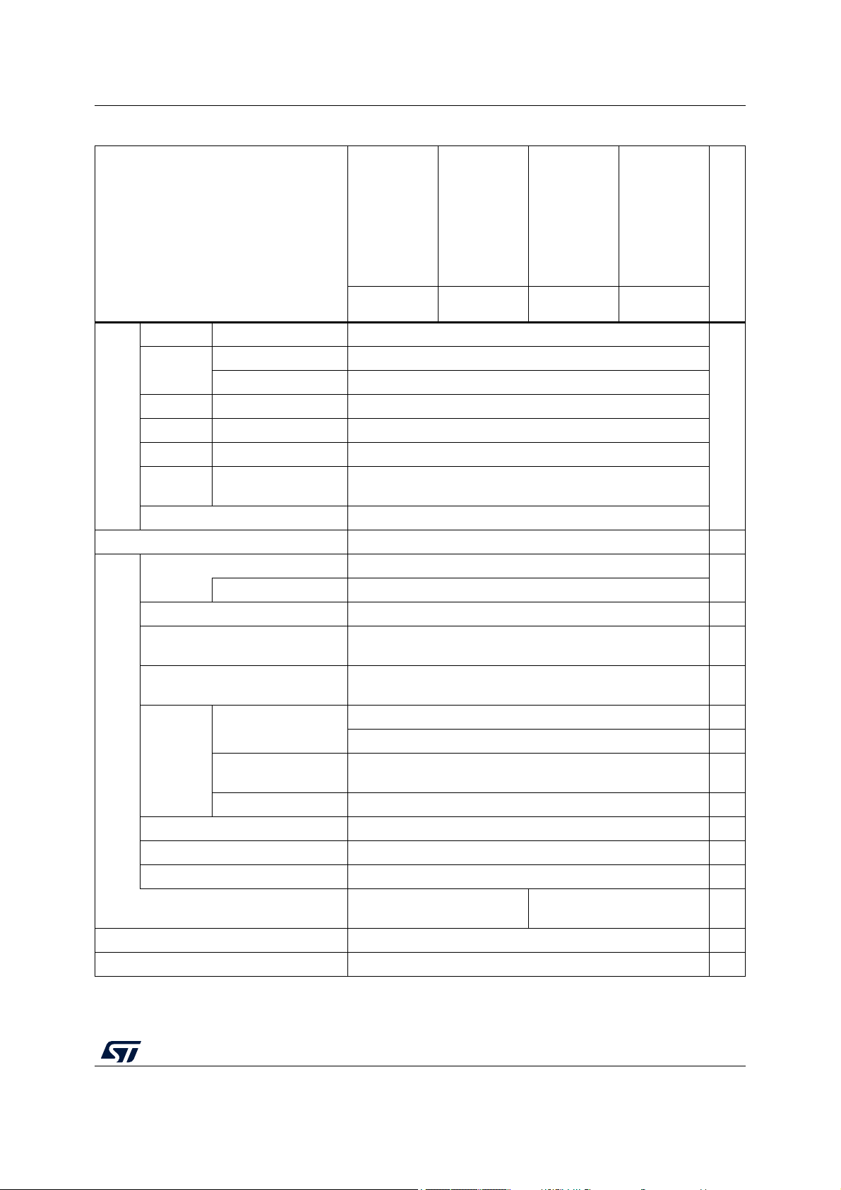
Figure 1. STM32MP157C/F block diagram . . . . . . . . . . . . . . . . . . . . . . . . . . . . . . . . . . . . . . . . . . . . 20
Figure 2. Power-up/down sequence . . . . . . . . . . . . . . . . . . . . . . . . . . . . . . . . . . . . . . . . . . . . . . . . . 30
Figure 3. STM32MP157C/F bus matrix . . . . . . . . . . . . . . . . . . . . . . . . . . . . . . . . . . . . . . . . . . . . . . . 37
Figure 4. Voltage reference buffer . . . . . . . . . . . . . . . . . . . . . . . . . . . . . . . . . . . . . . . . . . . . . . . . . . . 42
Figure 5. STM32MP157C/FADxx TFBGA257 pinout. . . . . . . . . . . . . . . . . . . . . . . . . . . . . . . . . . . . . 60
Figure 6. STM32MP157C/FABxx LFBGA354 pinout . . . . . . . . . . . . . . . . . . . . . . . . . . . . . . . . . . . . . 61
Figure 7. STM32MP157C/FACxx TFBGA361 pinout. . . . . . . . . . . . . . . . . . . . . . . . . . . . . . . . . . . . . 62
Figure 8. STM32MP157C/FAAxx LFBGA448 pinout . . . . . . . . . . . . . . . . . . . . . . . . . . . . . . . . . . . . . 63
Figure 9. Pin loading conditions. . . . . . . . . . . . . . . . . . . . . . . . . . . . . . . . . . . . . . . . . . . . . . . . . . . . 123
Figure 10. Pin input voltage . . . . . . . . . . . . . . . . . . . . . . . . . . . . . . . . . . . . . . . . . . . . . . . . . . . . . . . . 123
Figure 11. Power supply scheme. . . . . . . . . . . . . . . . . . . . . . . . . . . . . . . . . . . . . . . . . . . . . . . . . . . . 124
Figure 12. Current consumption measurement scheme . . . . . . . . . . . . . . . . . . . . . . . . . . . . . . . . . . 125
Figure 13. VDDCORE rise time from reset . . . . . . . . . . . . . . . . . . . . . . . . . . . . . . . . . . . . . . . . . . . . 130
Figure 14. VDDCORE rise time from LPLV-Stop. . . . . . . . . . . . . . . . . . . . . . . . . . . . . . . . . . . . . . . . 131
Figure 15. High-speed external clock source AC timing diagram (digital bypass) . . . . . . . . . . . . . . . 149
Figure 16. High-speed external clock source AC timing diagram (analog bypass) . . . . . . . . . . . . . . 150
Figure 17. Low-speed external clock source AC timing diagram (analog bypass) . . . . . . . . . . . . . . 151
Figure 18. Low-speed external clock source AC timing diagram . . . . . . . . . . . . . . . . . . . . . . . . . . . . 152
Figure 19. Typical application with a 24 MHz crystal . . . . . . . . . . . . . . . . . . . . . . . . . . . . . . . . . . . . . 153
Figure 20. Typical application with a 32.768 kHz crystal . . . . . . . . . . . . . . . . . . . . . . . . . . . . . . . . . . 154
Figure 21. PLL output clock waveforms in center spread mode . . . . . . . . . . . . . . . . . . . . . . . . . . . . 162
Figure 22. PLL output clock waveforms in down spread mode . . . . . . . . . . . . . . . . . . . . . . . . . . . . . 162
Figure 23. VIL/VIH for FT I/Os . . . . . . . . . . . . . . . . . . . . . . . . . . . . . . . . . . . . . . . . . . . . . . . . . . . . . . 168
Figure 24. Recommended NRST and NRST_CORE pin protection . . . . . . . . . . . . . . . . . . . . . . . . . 176
Figure 25. Asynchronous non-multiplexed SRAM/PSRAM/NOR read waveforms . . . . . . . . . . . . . . 177
Figure 26. Asynchronous non-multiplexed SRAM/PSRAM/NOR write waveforms . . . . . . . . . . . . . . 179
Figure 27. Asynchronous multiplexed PSRAM/NOR read waveforms. . . . . . . . . . . . . . . . . . . . . . . . 180
Figure 28. Asynchronous multiplexed PSRAM/NOR write waveforms . . . . . . . . . . . . . . . . . . . . . . . 182
Figure 29. Synchronous multiplexed NOR/PSRAM read timings . . . . . . . . . . . . . . . . . . . . . . . . . . . 184
Figure 30. Synchronous multiplexed PSRAM write timings. . . . . . . . . . . . . . . . . . . . . . . . . . . . . . . . 186
Figure 31. Synchronous non-multiplexed NOR/PSRAM read timings. . . . . . . . . . . . . . . . . . . . . . . . 188
Figure 32. Synchronous non-multiplexed PSRAM write timings . . . . . . . . . . . . . . . . . . . . . . . . . . . . 189
Figure 33. NAND controller waveforms for read access . . . . . . . . . . . . . . . . . . . . . . . . . . . . . . . . . . 191
Figure 34. NAND controller waveforms for write access . . . . . . . . . . . . . . . . . . . . . . . . . . . . . . . . . . 191
Figure 35. NAND controller waveforms for common memory read access . . . . . . . . . . . . . . . . . . . . 192
Figure 36. NAND controller waveforms for common memory write access. . . . . . . . . . . . . . . . . . . . 192
Figure 37. QUADSPI timing diagram - SDR mode . . . . . . . . . . . . . . . . . . . . . . . . . . . . . . . . . . . . . . 194
Figure 38. QUADSPI timing diagram - DDR mode . . . . . . . . . . . . . . . . . . . . . . . . . . . . . . . . . . . . . . 194
Figure 39. ADC accuracy characteristics . . . . . . . . . . . . . . . . . . . . . . . . . . . . . . . . . . . . . . . . . . . . . . 203
Figure 40. Typical connection diagram using the ADC . . . . . . . . . . . . . . . . . . . . . . . . . . . . . . . . . . . 203
Figure 41. 12-bit buffered /non-buffered DAC . . . . . . . . . . . . . . . . . . . . . . . . . . . . . . . . . . . . . . . . . . 207
Figure 42. Channel transceiver timing diagrams . . . . . . . . . . . . . . . . . . . . . . . . . . . . . . . . . . . . . . . . 213
Figure 43. DCMI timing diagram . . . . . . . . . . . . . . . . . . . . . . . . . . . . . . . . . . . . . . . . . . . . . . . . . . . . 214
Figure 44. LCD-TFT horizontal timing diagram . . . . . . . . . . . . . . . . . . . . . . . . . . . . . . . . . . . . . . . . . 216
Figure 45. LCD-TFT vertical timing diagram . . . . . . . . . . . . . . . . . . . . . . . . . . . . . . . . . . . . . . . . . . . 216
Figure 46. SPI timing diagram - slave mode and CPHA = 0 . . . . . . . . . . . . . . . . . . . . . . . . . . . . . . . 221
Figure 47. SPI timing diagram - slave mode and CPHA = 1
Figure 48. SPI timing diagram - master mode
(1)
. . . . . . . . . . . . . . . . . . . . . . . . . . . . . . . . . . . . . . . . 222
(1)
. . . . . . . . . . . . . . . . . . . . . . . . . . . . . 222
DS12505 Rev 5 11/260
12

List of figures STM32MP157C/F
Figure 49. I2S slave timing diagram (Philips protocol)
Figure 50. I2S master timing diagram (Philips protocol)
(1)
. . . . . . . . . . . . . . . . . . . . . . . . . . . . . . . . . . 224
(1)
. . . . . . . . . . . . . . . . . . . . . . . . . . . . . . . . . 224
Figure 51. SAI master timing waveforms . . . . . . . . . . . . . . . . . . . . . . . . . . . . . . . . . . . . . . . . . . . . . . 226
Figure 52. SAI slave timing waveforms . . . . . . . . . . . . . . . . . . . . . . . . . . . . . . . . . . . . . . . . . . . . . . . 226
Figure 53. MDIOS timing diagram . . . . . . . . . . . . . . . . . . . . . . . . . . . . . . . . . . . . . . . . . . . . . . . . . . . 227
Figure 54. SDIO high-speed mode . . . . . . . . . . . . . . . . . . . . . . . . . . . . . . . . . . . . . . . . . . . . . . . . . . 229
Figure 55. SD default mode . . . . . . . . . . . . . . . . . . . . . . . . . . . . . . . . . . . . . . . . . . . . . . . . . . . . . . . . 229
Figure 56. DDR mode . . . . . . . . . . . . . . . . . . . . . . . . . . . . . . . . . . . . . . . . . . . . . . . . . . . . . . . . . . . . 230
Figure 57. Ethernet MDIO/SMA timing diagram . . . . . . . . . . . . . . . . . . . . . . . . . . . . . . . . . . . . . . . . 231
Figure 58. Ethernet RMII timing diagram . . . . . . . . . . . . . . . . . . . . . . . . . . . . . . . . . . . . . . . . . . . . . . 232
Figure 59. Ethernet MII timing diagram . . . . . . . . . . . . . . . . . . . . . . . . . . . . . . . . . . . . . . . . . . . . . . . 233
Figure 60. Ethernet GMII timing diagram. . . . . . . . . . . . . . . . . . . . . . . . . . . . . . . . . . . . . . . . . . . . . . 234
Figure 61. Ethernet RGMII timing diagram . . . . . . . . . . . . . . . . . . . . . . . . . . . . . . . . . . . . . . . . . . . . 234
Figure 62. JTAG timing diagram . . . . . . . . . . . . . . . . . . . . . . . . . . . . . . . . . . . . . . . . . . . . . . . . . . . . 238
Figure 63. SWD timing. . . . . . . . . . . . . . . . . . . . . . . . . . . . . . . . . . . . . . . . . . . . . . . . . . . . . . . . . . . . 238
Figure 64. TFBGA257 - Outline . . . . . . . . . . . . . . . . . . . . . . . . . . . . . . . . . . . . . . . . . . . . . . . . . . . . . 239
Figure 65. TFBGA257 - Recommended footprint . . . . . . . . . . . . . . . . . . . . . . . . . . . . . . . . . . . . . . . 241
Figure 66. TFBGA257 marking (package top view). . . . . . . . . . . . . . . . . . . . . . . . . . . . . . . . . . . . . . 242
Figure 67. LFBGA354 - Outline . . . . . . . . . . . . . . . . . . . . . . . . . . . . . . . . . . . . . . . . . . . . . . . . . . . . . 243
Figure 68. LFBGA354 - Recommended footprint . . . . . . . . . . . . . . . . . . . . . . . . . . . . . . . . . . . . . . . 244
Figure 69. LFBGA354 marking (package top view) . . . . . . . . . . . . . . . . . . . . . . . . . . . . . . . . . . . . . . 245
Figure 70. TFBGA361 - Outline . . . . . . . . . . . . . . . . . . . . . . . . . . . . . . . . . . . . . . . . . . . . . . . . . . . . . 246
Figure 71. TFBGA361 - Recommended footprint . . . . . . . . . . . . . . . . . . . . . . . . . . . . . . . . . . . . . . . 248
Figure 72. TFBGA361 marking (package top view). . . . . . . . . . . . . . . . . . . . . . . . . . . . . . . . . . . . . . 249
Figure 73. LFBGA448 - Outline . . . . . . . . . . . . . . . . . . . . . . . . . . . . . . . . . . . . . . . . . . . . . . . . . . . . . 250
Figure 74. LFBGA448 - Recommended footprint . . . . . . . . . . . . . . . . . . . . . . . . . . . . . . . . . . . . . . . 251
Figure 75. LFBGA448 marking (package top view) . . . . . . . . . . . . . . . . . . . . . . . . . . . . . . . . . . . . . . 252
12/260 DS12505 Rev 5

STM32MP157C/F Introduction
1 Introduction
This datasheet provides the ordering information and mechanical device characteristics of
the STM32MP157C/F microprocessors.
This document should be read in conjunction with the STM32MP157 reference manual
(RM0436), available from the STMicroelectronics website www.st.com.
For information on the Arm
and Cortex
®
-M4 Technical Reference Manuals.
®(a)
Cortex®-A7 and Cortex®-M4 cores, refer to the Cortex®-A7
a. Arm is a registered trademark of Arm Limited (or its subsidiaries) in the US and/or elsewhere.
DS12505 Rev 5 13/260
59

Description STM32MP157C/F
2 Description
The STM32MP157C/F devices are based on the high-performance dual-core Arm®
®
Cortex
includes a 32-Kbyte L1 instruction cache for each CPU, a 32-Kbyte L1 data cache for each
CPU and a 256-Kbyte level2 cache. The Cortex-A7 processor is a very energy-efficient
application processor designed to provide rich performance in high-end wearables, and
other low-power embedded and consumer applications. It provides up to 20% more single
thread performance than the Cortex-A5 and provides similar performance than the CortexA9.
-A7 32-bit RISC core operating at up to 800 MHz. The Cortex-A7 processor
The Cortex-A7 incorporates all features of the high-performance Cortex-A15 and CortexA17 processors, including virtualization support in hardware, NEON
™
, and 128-bit AMBA®4
AXI bus interface.
The STM32MP157C/F devices also embed a Cortex
to 209 MHz frequency. Cortex-M4 core features a floating point unit (FPU) single precision
which supports Arm
®
Cortex
-M4 supports a full set of DSP instructions and a memory protection unit (MPU)
®
single-precision data-processing instructions and data types. The
®
-M4 32-bit RISC core operating at up
which enhances application security.
The STM32MP157C/F devices also embed a 3D graphic processing unit
(Vivante
®
- OpenGL® ES 2.0) running at up to 533 MHz, with performances up to 26
Mtriangle/s, 133 Mpixel/s.
The STM32MP157C/F devices provide an external SDRAM interface supporting external
memories up to 8-Gbit density (1 Gbyte), 16 or 32-bit LPDDR2/LPDDR3 or DDR3/DDR3L
up to 533 MHz.
The STM32MP157C/F devices incorporate high-speed embedded memories with
708 Kbytes of Internal SRAM (including 256 Kbytes of AXI SYSRAM, 3 banks of 128 Kbytes
each of AHB SRAM, 64 Kbytes of AHB SRAM in backup domain and 4 Kbytes of SRAM in
backup domain), as well as an extensive range of enhanced I/Os and peripherals connected
to APB buses, AHB buses, a 32-bit multi-AHB bus matrix and a 64-bit multi layer AXI
interconnect supporting internal and external memories access.
14/260 DS12505 Rev 5

STM32MP157C/F Description
All the devices offer two ADCs, two DACs, a low-power RTC, 12 general-purpose 16-bit
timers, two PWM timers for motor control, five low-power timers, a true random number
generator (RNG), and a cryptographic acceleration cell. The devices support six digital
filters for external sigma delta modulators (DFSDM). They also feature standard and
advanced communication interfaces.
• Standard peripherals
–Six I
2
Cs
– Four USARTs and four UARTs
– Six SPIs, three I
2
I
S peripherals can be clocked via a dedicated internal audio PLL or via an
2
Ss full-duplex master/slave. To achieve audio class accuracy, the
external clock to allow synchronization.
– Four SAI serial audio interfaces
– One SPDIF Rx interface
– Management data input/output slave (MDIOS)
– Three SDMMC interfaces
– An USB high-speed Host with two ports two high-speed PHYs and a USB OTG
high-speed with full-speed PHY or high-speed PHY shared with second port of
USB Host.
– Two FDCAN interface, including one supporting TTCAN mode
– A Gigabit Ethernet interface
– HDMI-CEC
• Advanced peripherals including
– A flexible memory control (FMC) interface
– A Quad-SPI Flash memory interface
– A camera interface for CMOS sensors
– An LCD-TFT display controller
– A DSI Host interface.
Refer to Tab le 1: STM32MP157C/F features and peripheral counts for the list of peripherals
available on each part number.
A comprehensive set of power-saving mode allows the design of low-power applications.
The STM32MP157C/F devices are proposed in 4 packages ranging from 257 to 448 balls
with pitch 0.5 mm to 0.8 mm. The set of included peripherals changes with the device
chosen.
These features make the STM32MP157C/F suitable for a wide range of consumer,
industrial, white goods and medical applications.
Figure 1 shows the general block diagram of the device family.
DS12505 Rev 5 15/260
59
Description STM32MP157C/F
Table 1. STM32MP157C/F features and peripheral counts
Features
STM32MP157CADxx
STM32MP157FADxx
STM32MP157CABxx
STM32MP157FABxx
STM32MP157CACxx
STM32MP157FACxx
STM32MP157CAAxx
STM32MP157FAAxx
TFBGA257 LFBGA354 TFBGA361 LFBGA448
Body size (mm) 10x10 16x16 12x12 18x18
Package
Pitch (mm) 0.5
(1)
0.8 0.5
Ball size (mm) 0.30 0.40 0.30 0.40
(1)
0.8
Thickness (mm) <1.2 <1.4 <1.2 <1.4
Ball count 257 354 361 448
CPU Dual-core Cortex-A7 FPU Neon TrustZone
2 × 32-Kbyte L1 data cache
Caches size
2 × 32-Kbyte L1 instruction cache
256-Kbyte level 2 unified coherent cache
Frequency
STM32MP157C: 2 × 650 MHz
STM32MP157F: 2 × 800 MHz
GPU Vivante - Open GL ES 2.0
for 3D graphics Frequency 533 MHz
MCU core Cortex-M4 FPU
Frequency 209 MHz
ROM 128 Kbytes (secure) -
Miscellaneous
-
-
-
-
CPU system 256 Kbytes (securable)
MCU subsystem 384 Kbytes
Embedded SRAM
MCU retention 64 Kbytes
Backup 4 Kbytes (securable, tamper protected)
16-bit 533 MHz Up to 1 Gbyte, single rank
LPDDR2/3
32-bit 533 MHz - -
SDRAM
DDR3/3L
(securable)
16-bit 533 MHz Up to 1 Gbyte, single rank
32-bit 533 MHz - -
Backup registers 128 bytes (32x32-bit, securable, tamper protected) -
16/260 DS12505 Rev 5
708 Kbytes
-
STM32MP157C/F Description
Table 1. STM32MP157C/F features and peripheral counts (continued)
Features
STM32MP157CADxx
STM32MP157FADxx
STM32MP157CABxx
STM32MP157FABxx
STM32MP157CACxx
STM32MP157FACxx
STM32MP157CAAxx
STM32MP157FAAxx
TFBGA257 LFBGA354 TFBGA361 LFBGA448
Advanced 16 bits 2
General
purpose
16 bits 8
32 bits 2
Basic 16 bits 2
Low power 16 bits 5
Timers
A7 timers 64 bits 2 × 4 (secure, non-secure, virtual, hypervisor)
M4
SysTick
24 bits 1
RTC/AWU 1 (securable)
Watchdog 3 (independent, independent secure, window) -
SPI 6 (1 securable)
Having I2S 3
I2C (with SMB/PMB support) 6 (2 securable) -
USART (smartcard, SPI, IrDA, LIN)
+ UART (IrDA, LIN)
SAI
4 (up to 8 audio channels), with I2S master/slave, PCM input,
4 + 4 (including 1 securable USART)
some can be a boot source
SPDIF-TX
Boot
Miscellaneous
29 timers
-
-
EHCI/OHCI Host
2 ports -
Embedded HS PHY with BCD -
USB
OTG HS/FS
(dual role port)
Yes, embedded FS or HS PHY with BCD, can be a boot source Boot
Embedded PHYs 3 (2 × high-speed + 1 × full-speed) -
Communication peripherals
SPDIF-RX 4 inputs -
FDCAN 2 (1 × TTCAN), clock calibration, 10 Kbyte shared buffer -
HDMI-CEC 1 -
Including the following securable 1 × USART, 1 × SPI, 2 × I2C
1 × USART, 1 × SPI, 2 × I2C
on securable GPIOs
-
SDMMC (SD, SDIO, e•MMC) 3 (8 + 8 + 4 bits), e•MMC or SD can be a boot source Boot
QuadSPI Yes (dual-quad), can be a boot source Boot
DS12505 Rev 5 17/260
59
Description STM32MP157C/F
Table 1. STM32MP157C/F features and peripheral counts (continued)
Features
STM32MP157CADxx
STM32MP157FADxx
STM32MP157CABxx
STM32MP157FABxx
STM32MP157CACxx
STM32MP157FACxx
STM32MP157CAAxx
STM32MP157FAAxx
TFBGA257 LFBGA354 TFBGA361 LFBGA448
Parallel address/data 8/16-bit - 4 × CS, up to 4 × 64 Mbyte
FMC
Parallel AD-Mux 8/16-bit 4 × CS, up to 4 × 64 Mbytes
boot
NAND 8/16-bit Yes, 1 × CS, SLC, BCH4/8, can be a boot source Boot
Gigabit Ethernet -
10/100M Ethernet MII, RMII with PTP and EEE
LCD-TFT Parallel interface
Display serial interface (DSI)
Up to 24-bit data, up to 90 MHz pixel clock
(up to 1366 × 768 60 fps or up to 1920 × 1080 30 fps)
2 × data lanes 1 GHz each
(up to 1366 × 768 60 fps or up to 1920 × 1080 30 fps)
MII, RMII, GMII, RGMII with
PTP and EEE
DMA 3 instances (1 securable), 48 physical channels in total -
Cryptography
Hash
dual instances (secure and non-secure)
dual instances (secure and non-secure)
DES, TDES, AES-256
SHA-256, MD5, HMAC
True random number generator True-RNG, dual instances (secure and non-secure) -
Fuses (one-time programmable) 3072 effective bits (secure, >1500 bits available for user) -
Camera interface Bus width 14-bit -
Miscellaneous
No
-
-
-
-
-
GPIOs with interrupt (total count) 98 148 176
Securable GPIOs - 8
-
Wakeup pins 4 6
Tamper pins (active tamper) 2 (1) 3 (1)
DFSDM 8 input channels with 6 filters -
Up to 16-bit synchronized ADC 2 (up to 3.6/4/4.5/5/6 Msps on 16/14/12/10/8-bit each)
Low noise 16 bit (differential) - 2 (1)
-
16 bit (differential) 17 (7) 20 (9)
ADC channels in total
(2)
17 22
12-bit DAC 2-
Internal ADC/DAC VREF 1.5 V, 1.8 V, 2.048 V, 2.5 V or VREF+ input
-
VREF+ input pin Yes
1. With inner matrix balls having 0.65 mm pitch to allow optimized PCB routing for supplies.
18/260 DS12505 Rev 5

STM32MP157C/F Description
2. In addition, there is also 6 internal channels for temperature, internal voltage reference, V
acquisitions.
DDCORE
, V
/4, DAC1 or DAC2
BAT
DS12505 Rev 5 19/260
59
Description STM32MP157C/F
MSv47445V4
@VDDA
@VDD_ANA
@VDDA
@VSW
@VDD
@VSW
@VDDA
@VSW
OTP Fuses
T
T
T
T
T
@VSW
SYSRAM 256KB
ROM 128KB
TIM3
ADC1
ADC2
64 bits
32 bits
32 bits
AXI
AHB
APB
64bits
AXI master
T
TrustZone
®
security protection
@VDD
Voltage Regulators
@VDD_ANA
Supply Supervision
32 bits
AHB master
BKPSRAM 4KB
STM
RETSRAM 64KB
DTS
(Digital temperature sensor)
@VDD_PLL
PLL1/2/3/4
@VDD
HSE (XTAL)
RCC
RNG2
DCMI
(Camera I/F)
MDIOS
CRC2
HSEM
PWR
SDMMC3
OTG
(HS/FS)
HASH2
T
USBPHYC
(USB 2 x PHY control)
FIFO
16b
16b
Interface
GPIOA
GPIOB
GPIOC
GPIOD
GPIOE
GPIOF
GPIOG
GPIOH
GPIOI
GPIOJ
GPIOK
16b
16b
16b
16b
16b
16b
16b
16b
16b
16b
8b
SRAM1 128KB
SRAM2 128KB
SRAM3/SRAM4 64K/64K
HSI
CSI LSI
DMA1
8 Streams
DMA2
8 Streams
FIFO FIFO
2
17
4
20
14
9
16
16
16
16
16
16
16
16
16
16
8
5
TIM4
16b
5
TIM6
16b
TIM7
16b
TIM12
16b
2
TIM13
16b
1
TIM14
16b
1
TIM2
32b
5
TIM5
32b
5
LPTIM1
16b
4
2
USART2
Smartcard
IrDA
5
USART3
Smartcard
IrDA
5
PLLUSB
FIFOFIFO
5
T
4b
10
PHY
FIFO
I2C4 / SMBUS
SPI6
USART1
IWDG1
BSEC
ETZPC
3
4
5
Smartcard
IrDA
FIFO FIFO
RTC / AWU
LSE (32kHz XTAL)
TAMP / Backup Regs
T
2
2
3
RNG1
HASH1
CRC1
T
T
LTDC
(LCD)
SDMMC1
31
29
14
SDMMC2
14
8b
8b
FIFO FIFOFIFO
MDMA
32 Channels
T
QUADSPI (dual)
DDRCTRL
LPDDR2/3
DDR3/3L
FMC
async
37
13
77
GPIOZ
8b
8
16b
AHB2APB
Trace port
APB1 (104.5 MHz)
APB3 (104.5 MHz)
T
24b
8b
AHB2APB
2x2
Matrix
AHB2APB
IC Supplies
16b
AXIM: ARM 64-bit AXI interconnect (266 MHz)
async
DLYBSD1
(SDMMC1 DLY control)
DLYBSD2
(SDMMC2 DLY control)
DLYBSD3
(SDMMC3 DLY control)
async
DLYBQS
(QUADSPI DLY control)
17
16b
FIFOFIFO
14b
DMAMUX1
DDRPHYC
AXIMC
T
TT
T
8KB
FIFO
Sys. Timing
GENeration
APB5 (133MHz)
debug TimeStamp
GENerator TSGEN
DLYDLY DLY
DLY
(R)(G)MII
32b PHY
APB4
MLAHB: ARM 32-bit multi-AHB bus matrix (209 MHz)
T
@VSW
IWDG2
T
I2C6 / SMBUS
3
USBH
(2 x HS Host)
2
2
2 x PHY
FIFO
STGENC
STGENR
EXTI
176
16ext
T
T
T
T
SYSCFG
VREFBUF
TIM1 / PWM
TIM8 / PWM
10
10
16b
16b
TIM15
4
16b
TIM16
16b
TIM17
16b
3
3
1
LPTIM2
16b
4
LPTIM3
16b
1
LPTIM4
16b
1
LPTIM5
16b
1
SAI4
13
FIFO
3
HDP
8
8b
SAI1
13
FIFO
SAI2
8
FIFO
SAI3
8
FIFO
UART4
4
UART5
4
UART7
4
UART8
4
DAC1
DAC2
12b
12b
Interface
1
1
I2C1 / SMBUS
3
Filter
I2C2 / SMBUS
3
Filter
I2C3 / SMBUS
3
Filter
I2C5 / SMBUS
3
Filter
CEC (HDMI-CEC)
SPDIFRX
1
4
SPI2 / I2S2
SPI3 / I2S3
5
5
FIFOFIFOFIFOFIFOFIFOFIFOFIFO
SPI4
4
SPI5
4
USART6
5
Smartcard
IrDA
FIFO FIFOFIFO
SPI1 / I2S1
5
FIFO
WWDG1
4ch
DFSDM1
17
8ch
AHB2APB
BOOT
pins
T
T
T
128 bits
CNT (Timer)
T
ETM
T
Cortex-A7 CPU
650/800
(1)
MHz + MMU +
FPU + NEON
T
32K I$
32K D$
T
ETH1 GMAC
10/100/1000
FIFO
DAP
(JTAG / SWD)
T
T
DDRPERFM
async
CRYP2
DAP bus
CRYP1
IPCC
T
TZC
T
T
FIFO
GPU
async
Shader
(533 MHz)
FDCAN1 (TT)
FDCAN2
Buffer 10KB CCU
2
2
APB2 (104.5 MHz)
APB2 (104.5 MHz)
APB2 (104.5 MHz)
PLLDSI
DSI
PHY
6
I-Bus
D-Bus
S-Bus
SYSTICK
NVIC
Cortex-M4 CPU 209 MHz
+ MPU + FPU
GIC
ETM
CNT (Timer)
T
T
Cortex-A7 CPU
650/800
(1)
MHz + MMU +
FPU + NEON
T
32K I$
32K D$
256KB L2$ + SCU
T
T
1. STM32MP157C: 650 MHz, STM32MP157F: 800 MHz
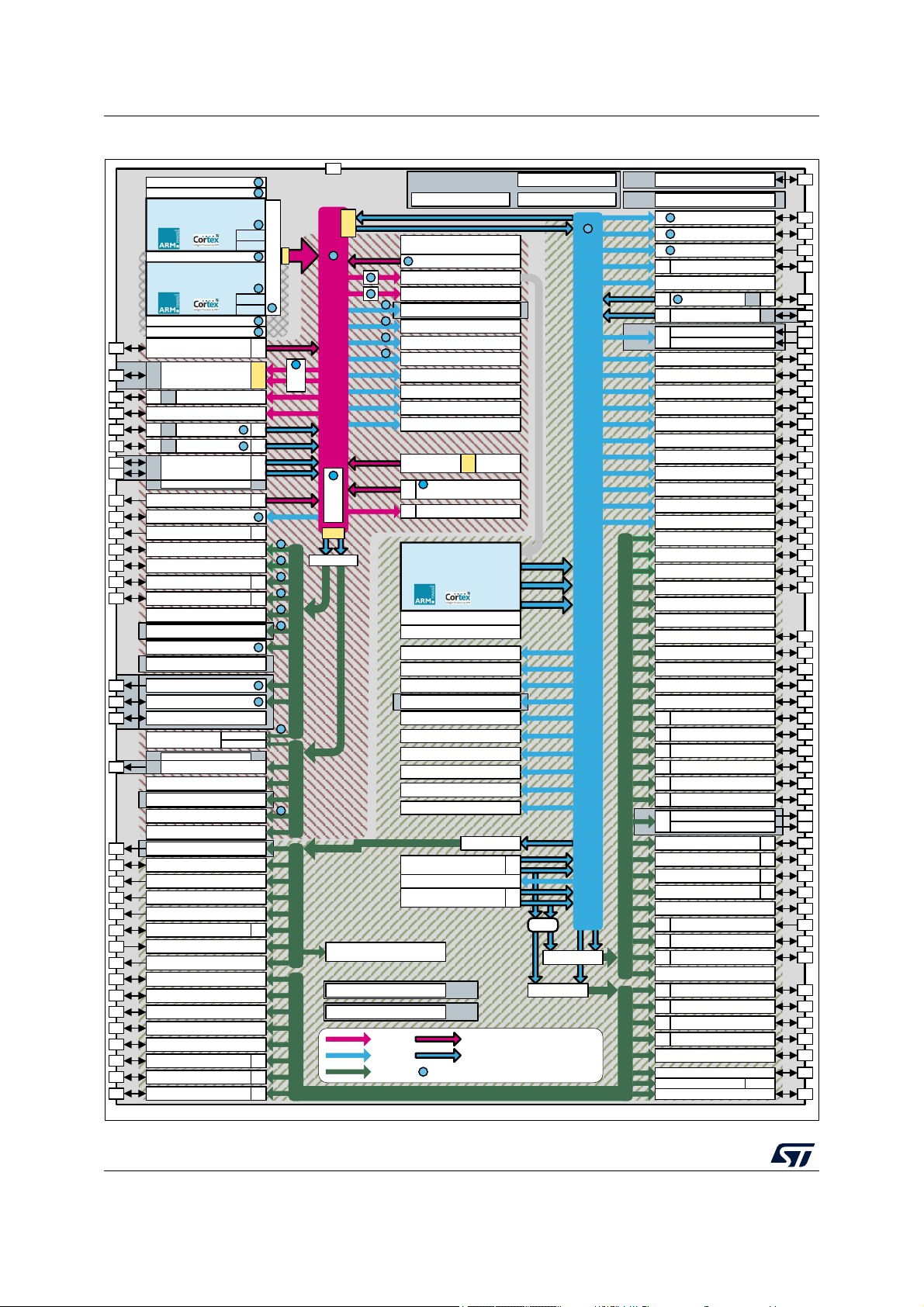
Figure 1. STM32MP157C/F block diagram
20/260 DS12505 Rev 5

STM32MP157C/F Functional overview
3 Functional overview
3.1 Dual-core Arm® Cortex®-A7 subsystem
3.1.1 Features
• ARMv7-A architecture
• 32-Kbyte L1 instruction cache for each CPU
• 32-Kbyte L1 data cache for each CPU
• 256-Kbyte level2 cache
• Arm
• Arm
• Arm
• DSP and SIMD extensions
• VFPv4 floating-point
• Hardware virtualization support
• Embedded trace module (ETM)
• Integrated generic interrupt controller (GIC) with 256 shared peripheral interrupts
• Integrated generic timer (CNT)
®
+ Thumb®-2 instruction set
®
TrustZone® security technology
®
NEON™ Advanced SIMD
3.1.2 Overview
The Cortex-A7 processor is a very energy-efficient applications processor designed to
provide rich performance in high-end wearables, and other low-power embedded and
consumer applications. It provides up to 20 % more single thread performance than the
Cortex-A5 and provides similar performance than the Cortex-A9.
The Cortex-A7 incorporates all features of the high-performance Cortex-A15 and CortexA17 processors, including virtualization support in hardware, NEON
AXI bus interface.
The Cortex-A7 processor builds on the energy-efficient 8-stage pipeline of the Cortex-A5
processor. It also benefits from an integrated L2 cache designed for low-power, with lower
transaction latencies and improved OS support for cache maintenance. On top of this, there
is improved branch prediction and improved memory system performance, with 64-bit loadstore path, 128-bit AMBA 4 AXI buses and increased TLB size (256 entry, up from 128 entry
for Cortex-A9 and Cortex-A5), increasing performance for large workloads such as web
browsing.
Thumb-2 technology
Delivers the peak performance of traditional Arm® code while also providing up to a 30 %
reduction in memory requirement for instructions storage.
TrustZone technology
Ensures reliable implementation of security applications ranging from digital rights
management to electronic payment. Broad support from technology and industry partners.
™
, and 128-bit AMBA®4
DS12505 Rev 5 21/260
59

Functional overview STM32MP157C/F
NEON
NEON technology can accelerate multimedia and signal processing algorithms such as
video encode/decode, 2D/3D graphics, gaming, audio and speech processing, image
processing, telephony, and sound synthesis. The Cortex-A7 provides an engine that offers
both the performance and functionality of the Cortex-A7 floating-point unit (FPU) and an
implementation of the NEON advanced SIMD instruction set for further acceleration of
media and signal processing functions. The NEON extends the Cortex-A7 processor FPU to
provide a quad-MAC and additional 64-bit and 128-bit register set supporting a rich set of
SIMD operations over 8-, 16- and 32-bit integer and 32-bit floating-point data quantities.
Hardware virtualization
Highly efficient hardware support for data management and arbitration, whereby multiple
software environments and their applications are able to simultaneously access the system
capabilities. This enables the realization of devices that are robust, with virtual environments
that are well isolated from each other.
Optimized L1 caches
Performance and power optimized L1 caches combine minimal access latency techniques
to maximize performance and minimize power consumption. There is also the option of
cache coherence for enhanced inter-processor communication, or support of a rich SMP
capable OS for simplified multicore software development.
Integrated L2 cache controller
Provides low-latency and high-bandwidth access to cached memory in high-frequency, or to
reduce the power consumption associated with off-chip memory access.
Cortex-A7 floating-point unit (FPU)
The FPU provides high-performance single and double precision floating-point instructions
compatible with the Arm VFPv4 architecture that is software compatible with previous
generations of Arm floating-point coprocessor.
Snoop control unit (SCU)
The SCU is responsible for managing the interconnect, arbitration, communication, cache to
cache and system memory transfers, cache coherence and other capabilities for the
processor.
This system coherence also reduces software complexity involved in maintaining software
coherence within each OS driver.
Generic interrupt controller (GIC)
Implementing the standardized and architected interrupt controller, the GIC provides a rich
and flexible approach to inter-processor communication and the routing and prioritization of
system interrupts.
Supporting up to 288 independent interrupts, under software control, each interrupt can be
distributed across A7 cores, hardware prioritized, and routed between the operating system
and TrustZone software management layer.
22/260 DS12505 Rev 5

STM32MP157C/F Functional overview
This routing flexibility and the support for virtualization of interrupts into the operating
system, provides one of the key features required to enhance the capabilities of a solution
utilizing a hypervisor.
3.2 Arm® Cortex®-M4 with FPU
The Arm® Cortex®-M4 with FPU core is a 32-bit RISC processor that features exceptional
code-efficiency, delivering the high-performance expected from an Arm core in the memory
size usually associated with 8- and 16-bit devices.
The processor supports a set of DSP instructions which allow efficient signal processing and
complex algorithm execution.
Its single precision FPU (floating point unit) speeds up software development by using
metalanguage development tools, while avoiding saturation.
Note: Cortex-M4 with FPU core is binary compatible with the Cortex-M3 core.
Memory protection unit (MPU)
The memory protection unit (MPU) manages the Cortex®-M4 access rights and the
attributes of the system resources. It has to be programmed and enabled before use. Its
main purposes are to prevent an untrusted user program to accidentally corrupt data used
by the OS and/or by a privileged task, but also to protect data processes or read-protect
memory regions.
The MPU defines access rules for privileged accesses and user program accesses. It
allows the definition of up to 16 protected regions that can in turn be divided into up to 8
independent subregions, where region address, size, and attributes can be configured. The
protection area ranges from 32 bytes to 4
When an unauthorized access is performed, a memory management exception is
generated.
Gbytes of addressable memory.
3.3 Graphic processing unit (GPU)
The STM32MP157C/F includes a 3D graphics engine (Vivante).
The GPU is a dedicated graphics processing unit accelerating numerous 3D graphics
applications such as graphical user interface (GUI), menu display or animations.
It works together with an optimized software stack design for industry-standard APIs with
support for Android™ and Linux
®
embedded development platforms.
DS12505 Rev 5 23/260
59

Functional overview STM32MP157C/F
Hardware features:
• OpenGL ES 2.0 / 1.1 compliance, including extensions; OpenVG 1.1
• IEEE 32-bit floating-point pipeline
• Ultra-threaded, unified vertex and fragment (pixel) shaders
• Low memory bandwidth at both high and low data rates
• Low CPU loading
• Up to 12 programmable elements per vertex
• Dependent texture operation with high-performance
• Alpha blending
• Depth and stencil compare
• Support for 8 fragment shader simultaneous textures
• Support for 4 vertex shader simultaneous textures
• Point sampling, bi-linear sampling, tri-linear filtering, and cubic textures
• 8 k x 8 k texture size and 8 k x 8 k rendering target
• 4 Vertex DMA streams
API support:
• OpenGL ES 1.1 and 2.0
• OpenVG 1.1
• EGL 1.4
• OpenGL 2.1
Performance up to:
• 26 Mtriangle/s
• 133 Mpixel/s
24/260 DS12505 Rev 5

STM32MP157C/F Functional overview
3.4 Memories
3.4.1 External SDRAM
The STM32MP157C/F devices embed a controller for external SDRAM which support the
following devices
• LPDDR2 or LPDDR3, 16- or 32-bit data, up to 1 Gbyte, up to 533 MHz clock.
• DDR3 or DDR3L, 16- or 32-bit data, up to 1 Gbyte, up to 533 MHz clock.
3.4.2 Embedded SRAM
All devices feature:
• SYSRAM in MPU domain: 256 Kbytes
• SRAM1 in MCU domain: 128 Kbytes
• SRAM2 in MCU domain: 128 Kbytes
• SRAM3 in MCU domain: 64 Kbytes
• SRAM4 in MCU domain: 64 Kbytes
• RETRAM (retention RAM): 64 Kbytes
The content of this area can be retained in Standby or V
• BKPSRAM (backup SRAM): 4 Kbytes
The content of this area is protected against possible unwanted write accesses, and
can be retained in Standby or V
BAT
mode.
BKPSRAM can be defined (in ETZPC) as accessible by secure software only.
BAT
mode.
DS12505 Rev 5 25/260
59

Functional overview STM32MP157C/F
3.5 DDR3/DDR3L/LPDDR2/LPDDR3 controller (DDRCTRL)
DDRCTRL combined with DDRPHYC provides a complete memory interface solution for
DDR memory subsystem.
• Two 64-bit AMBA 4 AXI4 ports interface (XPI)
• AXI clock asynchronous to the controller
• Supported standards:
– JEDEC DDR3 SDRAM specification, JESD79-3E for DDR3/3L with 32-bit
interface
– JEDEC LPDDR2 SDRAM specification, JESD209-2E for LPDDR2 with 32-bit
interface
– JEDEC LPDDR3 SDRAM specification, JESD209-3B for LPDDR3 with 32-bit
interface
• Advanced scheduler and SDRAM command generator
• Programmable full data width (32-bit) or half data width (16-bit)
• Advanced QoS support with 3 traffic class on read and 2 traffic classes on write
• Options to avoid starvation of lower priority traffic
• Guaranteed coherency for write-after-read (WAR) and read-after-write (RAW) on AXI
ports
• Programmable support for burst length options (4, 8,16)
• Write combine to allow multiple writes to the same address to be combined into a
single write
• Single rank configuration
• Supports automatic SDRAM power-down entry and exit caused by lack of transaction
arrival for programmable time
• Supports automatic clock stop (LPDDR2/3) entry and exit caused by lack of transaction
arrival
• Supports automatic low power mode operation caused by lack of transaction arrival for
programmable time via hardware low power interface
• Programmable paging policy
• Supports automatic or under software control self-refresh entry and exit
• Support for deep power-down entry and exit under software control (LPDDR2)
• Support for explicit SDRAM mode register updates under software control
• Flexible address mapper logic to allow application specific mapping of row, column,
bank bits
• User-selectable refresh control options
• DDRPERFM associated block to help for performance monitoring and tuning
DDRCTRL and DDRPHYC can be defined (in ETZPC) as accessible by secure software
only.
26/260 DS12505 Rev 5

STM32MP157C/F Functional overview
3.6 TrustZone address space controller for DDR (TZC)
TZC is used to filter read/write accesses to DDR controller according to TrustZone rights
and according to non-secure master (NSAID) on up to 9 programmable regions.
• Configuration is supported by trusted software only
• 2 filter units working concurrently
• 9 regions:
– region 0 is always enabled and covers the whole address range.
– regions 1 to 8 have programmable base/end address and can be assigned to any
one or both filters.
• Secure and non-secure access permissions programmed per region
• Non-secure accesses are filtered according to NSAID
• Regions controlled by same filter must not overlap
• Fail modes with error and/or interrupt
• Acceptance capability = 256
• Gate keeper logic to enable and disable of each filter
• Speculative accesses
DS12505 Rev 5 27/260
59
Functional overview STM32MP157C/F
3.7 Boot modes
At startup, the boot source used by the internal BootROM is selected by the BOOT pin and
OTP bytes.
BOOT2 BOOT1 BOOT0 Initial boot mode Comments
Table 2. Boot modes
Wait incoming connection on:
(3)
(1)
– USART2/3/6 and UART4/5/7/8 on default pins
– USB high-speed device
(3)
Serial NOR Flash on QUADSPI
e•MMC on SDMMC2 (default)
(2)
(4)
(4)(5)
SLC NAND Flash on FMC
0 0 0 UART and USB
0 0 1 Serial NOR Flash
010e•MMC
(3)
011NAND Flash
1 0 0 Reserved (NoBoot) Used to get debug access without boot from Flash memory
101SD card
(3)
SD card on SDMMC1 (default)
(4)(5)
Wait incoming connection on:
1 1 0 UART and USB
(1)(3)
– USART2/3/6 and UART4/5/7/8 on default pins
– USB high-speed device on OTG_HS_DP/DM pins
1 1 1 Serial NAND Flash
1. can be disabled by OTP settings.
2. USB requires 24 MHz HSE clock/crystal if OTP is not programmed for different frequency.
3. Boot source can be changed by OTP settings (e.g. initial boot on SD card, then e•MMC with OTP settings).
4. Default pins can be altered by OTP.
5. Alternatively, another SDMMC1 or SDMMC2 interface than this default can be selected by OTP.
(3)
Serial NAND Flash on QUADSPI
(4)
(2)
28/260 DS12505 Rev 5

STM32MP157C/F Functional overview
3.8 Power supply management
3.8.1 Power supply scheme
Caution: V
• The V
is the main supply for I/Os and internal part kept powered during Standby
DD
mode. Useful voltage range is 1.71 V to 3.6 V (e.g. 1.8 V, 2.5 V, 3.0 V or 3.3 V typ.)
–V
• The V
DDCORE
DD_DSI
, V
DD_PLL
and V
DD_ANA
must be star-connected to VDD.
is the main digital voltage and is usually shutdown during Standby mode.
Voltage range during Run mode is 1.18 V to 1.25/1.38 V (1.2/1.34 V typ.), see
Table 13: General operating conditions.
• The VBAT pin can be connected to the external battery (1.2 V < V
external battery is used, it is mandatory to connect this pin to V
DD
BAT
.
< 3.6 V). If no
• The VDDA pin is the analog (ADC/DAC/VREF), supply voltage range is 1.71 V to 3.6 V.
DAC can only be used when V
requires V
equal to or higher than V
DDA
is above or equal 1.8 V. Using Internal V
DDA
REF+
+ 0.3 V.
REF+
• The VDDA1V8_REG pin is the output of internal regulator and connected internally to
USB PHY and USB PLL. Internal V
DDA1V8_REG
regulator is enabled by default and can
be controlled by software. It is always shut down during Standby mode.
There is specific BYPASS_REG1V8 pin that must be connected either to V
or VDD to
SS
activate or deactivate the voltage regulator. It is mandatory to bypass the 1.8 V
regulator when V
VDDA1V8_REG pin must be connected to V
is below 2.25 V (BYPASS_REG1V8 = V
DD
(if below 1.98 V) or to a dedicated
DD
. In that case,
DD)
1.65 V - 1.98 V supply (1.8 V typ.).
• V
DDA1V8_DSI
Should be connected to V
is the analog DSI supply. Voltage range is 1.65 V to 1.98 V. (1.8 V typ.)
DDA1V8_REG
.
• VDDA1V1_REG pin is the output of internal regulator connected internally to USB PHY.
Internal V
DDA1V1_REG
regulator is enabled by default and can be controlled by
software. It is always shut down during Standby mode.
• VDDA1V2_DSI_REG pin is the output of internal regulator and connected internally to
DSI PLL.
• V
DDA1V2_DSI_PHY
V
DDA1V2_DSI_REG
• V
DD3V3_USBHS
PHY supply. Voltage range is 3.07 V to 3.6 V. V
OTG_VBUS and ID pins. So, V
speed OTG device is used. If not used, must be connected to V
DD3V3_USBHS
must not be present unless V
is the analog DSI PHY supply and should be connected to
.
and V
DD3V3_USBFS
are respectively the USB high-speed and full-speed
is used to supply
DD.
DD3V3_USBFS
DDA1V8_REG
DD3V3_USBFS
must be supplied as well when USB high-
is present, otherwise permanent
STM32MP157C/F damage could occur. Must be ensured by PMIC ranking order or with
external component in case of discrete component power supply implementation.
• V
DDQ_DDR
is the DDR IO supply.
– Voltage range is 1.425 V to 1.575 V for interfacing DDR3 memories (1.5 V typ.).
– Voltage range is 1.283 V to 1.45 V for interfacing DDR3L memories (1.35 V typ.).
– Voltage range is 1.14 V to 1.3 V for interfacing LPDDR2 or LPDDR3 memories
(1.2 V typ.).
DS12505 Rev 5 29/260
59
Functional overview STM32MP157C/F
MSv47490V1
0.3
1
V
BOR0
3.6
Operating modePower-on Power-down time
V
V
DDX
(1)
V
DD
Invalid supply area V
DDX
< V
DD
+ 300 mV
V
DDX
independent from V
DD
During power-up and power-down phases, the following power sequence requirements
must be respected:
• When VDD is below 1 V, other power supplies (V
V
DDA1V8_DSI
V
+ 300 mV.
DD
• When V
During the power-down phase, V
, V
DDA1V1_REG
is above 1 V, all power supplies are independent.
DD
, V
DD3V3_USBHS/FS
can temporarily become lower than other supplies only
DD
, V
DDCORE
DDQ_DDR
, V
, V
DDA
DDA1V8_REG
) must remain below
,
if the energy provided to the STM32MP157C/F device remains below 1 mJ; this allows
external decoupling capacitors to be discharged with different time constants during the
power- down transient phase.
Figure 2. Power-up/down sequence
1. V
refers to any power supply among V
DDX
V
DD3V3_USBHS/FS
, V
DDQ_DDR
, V
.
DDCORE
DDA
, V
DDA1V8_REG
, V
DDA1V8_DSI
, V
DDA1V1_REG
,
30/260 DS12505 Rev 5

STM32MP157C/F Functional overview
3.8.2 Power supply supervisor
The devices have an integrated power-on reset (POR)/ power-down reset (PDR) circuitry
coupled with a Brownout reset (BOR) circuitry:
• Power-on reset (POR)
The POR supervisor monitors V
The devices remain in reset mode when V
• Power-down reset (PDR)
The PDR supervisor monitors V
below a fixed threshold.
The PDR supervisor can be enabled/disabled through PDR_ON pin.
• Brownout reset (BOR)
The BOR supervisor monitors V
2.7 V) can be configured through option bytes. A reset is generated when V
below this threshold.
• Power-on reset V
DDCORE
(POR_VDDCORE)
The POR_VDDCORE supervisor monitors V
a fixed threshold. The V
DDCORE
this threshold,
• Power-down reset V
DDCORE
The PDR_VDDCORE supervisor monitors V
reset is generated when V
DDCORE
The PDR_VDDCORE supervisor can be enabled/disabled through PDR_ON_CORE
pin.
power supply and compares it to a fixed threshold.
DD
power supply. A reset is generated when V
DD
power supply. Three BOR thresholds (from 2.1 to
DD
domain remain in reset mode when V
is below this threshold,
DD
DDCORE
power supply and compares it to
DDCORE
(PDR_VDDCORE)
DDCORE
power supply. A V
DDCORE
drops below a fixed threshold.
drops
DD
drops
DD
is below
domain
DS12505 Rev 5 31/260
59

Functional overview STM32MP157C/F
3.9 Low-power strategy
There are several ways to reduce power consumption on STM32MP157C/F:
• Decrease dynamic power consumption by slowing down the CPU clocks and/or the
bus matrix clocks and/or controlling individual peripheral clocks.
• Save power consumption when the CPU is IDLE, by selecting among the available lowpower mode according to the user application needs. This allows the best compromise
between short startup time, low-power consumption, as well as available wakeup
sources, to be achieved.
The CPUs feature several low-power modes:
• CSleep (CPU clock stopped)
• CStop (CPU sub-system clock stopped)
• Stop (bus matrix clocks stalled, the oscillators can be stopped)
• CStandby (MPU sub-system clock stopped and wakeup via reset)
• Standby (system powered down)
• LP-Stop and LPLV-Stop (bus matrix clocks stalled, the oscillators can be stopped, low-
power mode signaled to external regulator)
CSleep and CStop low-power modes are entered by the CPU when executing the WFI (wait
for interrupt) or WFE (Wait for Event) instructions, or when the SLEEPONEXIT bit of the
Cortex-M4 core is set after returning from an interrupt service routine.
If part of the domain is not in low-power mode, the domain remains in the current mode.
Finally the system can enter Stop or Standby when all EXTI wakeup sources are cleared
and the CPUs are in CStop or CStandby mode.
System power mode MPU MCU
Run mode
Stop mode
LP-Stop mode
LPLV-Stop mode
Standby mode
Table 3. System versus domain power mode
CRun or CSleep
CStop or CStandby
CRun or CSleep CStop
CStop or CStandby CStop
CStandby or (CStop and
MPU PDDS = 1 and MPU CSTBYDIS = 1)
CRun or CSleep
CStop and
MCU PDDS = 1
32/260 DS12505 Rev 5

STM32MP157C/F Functional overview
3.10 Reset and clock controller (RCC)
The clock and reset controller manages the generation of all the clocks, as well as the clock
gating and the control of the system and peripheral resets. It provides a high flexibility in the
choice of clock sources and allows application of clock ratios to improve the power
consumption. In addition, on some communication peripherals that are capable to work with
two different clock domains (either a bus interface clock or a kernel peripheral clock), the
system frequency can be changed without modifying the baudrate.
3.10.1 Clock management
The devices embed four internal oscillators, two oscillators with external crystal or
resonator, three internal oscillators with fast startup time and four PLLs.
The RCC receives the following clock source inputs:
• Internal oscillators:
– 64 MHz HSI clock (1% accuracy)
– 4 MHz CSI clock
– 32 kHz LSI clock
• External oscillators:
– 8-48 MHz HSE clock
– 32.768 kHz LSE clock
The RCC provides four PLLs:
• The PLL1 is dedicated to the MPU clocking
• The PLL2 provides:
– The clocks for the AXI-SS (including APB4, APB5, AHB5 and AHB6 bridges)
– The clocks for the DDR interface
– The clocks for the GPU
• The PLL3 provides:
– The clocks for the MCU, and its bus matrix (including the APB1, APB2, APB3,
AHB1, AHB2, AHB3 and AHB4)
– The kernel clocks for peripherals
• The PLL4 is dedicated to the generation of the kernel clocks for various peripherals
The system starts on the HSI clock. The user application can then select the clock
configuration.
DS12505 Rev 5 33/260
59

Functional overview STM32MP157C/F
3.10.2 System reset sources
The power-on reset initializes all registers while the system reset reinitializes the system
except for the debug, part of the RCC and power controller status registers, as well as the
backup power domain.
An application reset is generated from one of the following sources:
– a reset from NRST pad
– a reset from POR and PDR signal (generally called power-on reset)
– a reset from BOR (generally called brownout)
– a reset from the independent watchdogs 1
– a reset from the independent watchdogs 2
– a software reset from the Cortex-M4 (MCU)
– a software reset from the Cortex-A7 (MPU)
– a failure on HSE, when the clock security system feature is activated
A system reset is generated from one of the following sources:
– An application reset,
– A reset from POR_VDDCORE signal,
– Every time the system exits from Standby.
3.11 Hardware semaphore (HSEM)
The HW semaphore block provides 64 (32-bit) register-based semaphores.
The semaphores can be used to ensure synchronization between different processes
running on a core and between different cores. The HSEM provides a non blocking
mechanism to lock semaphores in an atomic way. The following functions are provided:
• Locking a semaphore can be done in 2 ways:
– 2-step lock: by writing CoreID and ProcessID to the semaphore, followed by a
read check.
– 1-step lock: by reading the CoreID from the semaphore.
• Interrupt generation when a semaphore is freed.
– Each semaphore may generated an interrupt on one of the interrupt lines.
• Semaphore clear protection.
– A semaphore is only cleared when CoreID and ProcessID matches.
• Global semaphore clear per CoreID.
3.12 Inter-processor communication controller (IPCC)
The inter-processor communication controller (IPCC) is used for communicating data
between two processors.
The IPCC block provides a non blocking signaling mechanism to post and retrieve
communication data in an atomic way. It provides the signaling for four channels:
• two channels in the direction from processor 1 to processor 2
• two channels in the opposite direction.
34/260 DS12505 Rev 5

STM32MP157C/F Functional overview
It is then possible to have two different communication types in each direction.
The IPCC communication data must be located in a common memory, which is not part of
the IPCC block.
3.12.1 IPCC main features
• Status signaling for the four channels
– Channel occupied/free flag, also used as lock
• Two interrupt lines per processor
– One for RX channel occupied (communication data posted by sending processor)
– One for TX channel free (communication data retrieved by receiving processor)
• Interrupt masking per channel
– Channel occupied mask
– Channel free mask
• Two channel operation modes
– Simplex (each channel has its own communication data memory location)
– Half duplex (a single channel in associated to a bidirectional communication data
information memory location)
3.13 General-purpose input/outputs (GPIOs)
Each of the GPIO pins can be configured by software as output (push-pull or open-drain,
with or without pull-up or pull-down), as input (with or without pull-up or pull-down) or as
peripheral alternate function. Most of the GPIO pins are shared with digital or analog
alternate functions. All GPIOs are high-current-capable and have speed selection to better
manage internal noise, power consumption and electromagnetic emission.
After reset, all GPIOs are in analog mode to reduce power consumption.
The I/O configuration can be locked if needed by following a specific sequence in order to
avoid spurious writing to the I/Os registers.
Additionally, GPIO pins on port Z can be individually set as secure, which would mean that
software accesses to these GPIOs and associated peripherals defined as secure are
restricted to secure software running on Cortex-A7.
3.14 TrustZone protection controller (ETZPC)
ETZPC is used to configure TrustZone security of bus masters and slaves with
programmable-security attributes (securable resources) such as:
• On-chip SYSRAM with programmable secure region size
• AHB and APB peripherals to be made secure
Notice that by default, SYSRAM and peripheral are set to secure access only, so, not
accessible by non-secure masters such as Cortex-M4 or DMA1/DMA2.
ETZPC can also allocate peripherals and SRAM to be accessible only by the Cortex-M4
and/or DMA1/DMA2. This ensures the safe execution of the Cortex-M4 firmware, protected
from other masters (e.g. Cortex-A7) unwanted accesses.
DS12505 Rev 5 35/260
59

Functional overview STM32MP157C/F
3.15 Bus-interconnect matrix
The devices feature an AXI bus matrix, one main AHB bus matrix and bus bridges that allow
bus masters to be interconnected with bus slaves (see Figure 3, the dots represent the
enabled master/slave connections).
36/260 DS12505 Rev 5

STM32MP157C/F Functional overview
MSv47453V2
MCU_AHB2
MCU_AHB_MPU
MCU_AHB_RET
MCU_AHB3
MCU_AHB_MEM2
MCU_AHB4
MCU_AHB_MEM1
MCU_AHB_MEM0
S-BUS
D-BUS
I-BUS
MPU_AXI_FMC
MPU_AXI_QUADSPI
MPU_AXI_SYSRAM
MPU_AXI_DDR1
MPU_AHB_MCU
MPU_AHB6
MPU_AXI_ROM
MPU_AHB5
MPU_APB5
MPU_AXI_STM
MPU_AXI_DDR2
MPU_DBG_APB
128-bit
Interconnect AHB 32 bits 209 MHz - 10 masters / 9 slaves
NIC-400 AXI 64 bits 266 MHz - 11 masters / 12 slaves
FMC/NAND
DDRCTRL 533 MHz
APB bridge to APB5
APB bridge to DBG APB
QUADSPI
SYSRAM 256 KB
ROM 128 KB
STM
AHB bridge to AHB5
AHB bridge to AHB6
S1
S2
S3
S4
S5
S6
S7
S9
S10
S8
S0
S11
AHB 32 synchronous master port
AXI 64 synchronous master port
AXI 64 synchronous slave port
AXI 64 asynchronous master port
AXI 64 asynchronous slave port
AHB 32 synchronous slave port
AHB 32 asynchronous master port
AHB 32 asynchronous slave port
Masters access S0 XOR S1 layer
SDMMC1
MDMA
LTDC
Default
slave
CPU
SDMMC2
AXIM
From MCU
interconnect
ETH
DBG
USBH
M0 M1 M2 M3 M4 M5 M6 M7 M9M10
GPU 533 MHz
M8
AXIMC
To MCU interconnect
Bridge to AHB3
Bridge to AHB2
RetentionRAM
Bridge to AHB4
SRAM3
S1
S2
S3
S4
S5
S6
S7
S0
USBO
SDMMC3
CM4
From MPU
interconnect
DMA1
M1 M2 M3 M4 M5 M6 M7 M8M0 M9
To MPU interconnect
DMA2
SRAM1
SRAM2
MLAHB
MCU_AHB_MEM3
SRAM4
S8
Figure 3. STM32MP157C/F bus matrix
DS12505 Rev 5 37/260
59

Functional overview STM32MP157C/F
3.16 DMA controllers
The devices features three DMA modules to unload CPU activity:
• A master direct memory access (MDMA)
The MDMA is a high-speed DMA controller, which is in charge of all types of memory
transfers (peripheral to memory, memory to memory, memory to peripheral), without
any CPU action. It features a master AXI interface.
The MDMA is located in MPU domain. It is able to interface with the other DMA
controllers located in MCU domain to extend the standard DMA capabilities, or can
manage peripheral DMA requests directly.
Each of the 32 channels can perform block transfers, repeated block transfers and
linked list transfers.
The MDMA can be set to make secure transfers to secured memories.
• Two DMA controllers (DMA1, DMA2), located in MCU domain. Each controller is a
dual-port AHB, for a total of 16 DMA channels to perform FIFO-based block transfers.
The DMAMUX is an extension of the DMA1 and DMA2 controllers. It multiplexes and routes
the DMA peripheral requests to the DMA1 or DMA2 controllers, with a high flexibility,
maximizing the number of DMA requests that run concurrently, as well as generating DMA
requests from peripheral output trigger or DMA event.
3.17 Nested vectored interrupt controller (NVIC)
The devices embed a nested vectored interrupt controller able to manage 16 priority levels,
and handle up to 150 maskable interrupt channels plus the 16 interrupt lines of the Cortex
M4 with FPU core.
• Closely coupled NVIC gives low-latency interrupt processing
• Interrupt entry vector table address passed directly to the core
• Allows early processing of interrupts
• Processing of late arriving, higher-priority interrupts
• Support tail chaining
• Processor context automatically saved
• Interrupt entry restored on interrupt exit with no instruction overhead
This hardware block provides flexible interrupt management features with minimum interrupt
latency.
3.18 Extended interrupt and event controller (EXTI)
The extended interrupt and event controller (EXTI) manages individual CPU and system
wakeup through configurable and direct event inputs. It provides wake-up requests to the
power control, and generates an interrupt request to the CPUs NVIC or GIC and events to
the CPUs event inputs. For each CPU an additional event generation block (EVG) is needed
to generate the CPU event signal.
®
-
The EXTI wake-up requests allow the system to be woken up from Stop mode, and the
CPUs to be woken up from CStop and CStandby modes.
The interrupt request and event request generation can also be used in Run mode.
38/260 DS12505 Rev 5

STM32MP157C/F Functional overview
The block also includes the EXTI IOport selection.
Each interrupt or event can be set as secure in order to restrict access to secure software
only.
3.19 Cyclic redundancy check calculation unit (CRC1, CRC2)
The CRC (cyclic redundancy check) calculation unit is used to get a CRC code using a
programmable polynomial.
Among other applications, CRC-based techniques are used to verify data transmission or
storage integrity. In the scope of the EN/IEC 60335-1 standard, they offer a means of
verifying the Flash memory integrity. The CRC calculation unit helps computing a signature
of the software during runtime, to be compared with a reference signature generated at linktime and stored at a given memory location.
3.20 Flexible memory controller (FMC)
The FMC controller main features are the following:
• Interface with static-memory mapped devices including:
– NOR Flash memory
– Static or pseudo-static random access memory (SRAM, PSRAM)
– NAND Flash memory with 4-bit/8-bit BCH hardware ECC
• 8-,16-bit data bus width
• Independent chip select control for each memory bank
• Independent configuration for each memory bank
• Write FIFO
3.21 Dual Quad-SPI memory interface (QUADSPI)
The QUADSPI is a specialized communication interface targeting single, dual or quad SPI
Flash memories. It can operate in any of the three following modes:
• indirect mode: all the operations are performed using the QUADSPI registers
• status polling mode: the external Flash memory status register is periodically read and
an interrupt can be generated in case of flag setting
• memory-mapped mode: the external Flash memory is mapped to the address space
and is seen by the system as if it was an internal memory
Both throughput and capacity can be increased two-fold using dual-flash mode, where two
Quad-SPI Flash memories are accessed simultaneously.
QUADSPI is coupled with a delay block (DLYBQS) allowing the support of external data
frequency above 100 MHz.
DS12505 Rev 5 39/260
59

Functional overview STM32MP157C/F
3.22 Analog-to-digital converters (ADCs)
The STM32MP157C/F devices embed two analog-to-digital converters, which resolution
can be configured to 16, 14, 12, 10 or 8 bits. Each ADC shares up to 20 external channels,
performing conversions in the single-shot or scan mode. In scan mode, automatic
conversion is performed on a selected group of analog inputs.
Additional logic functions embedded in the ADC interface allow:
• simultaneous ADC1/ADC2 conversion
• interleaved ADC1/ADC2 conversion.
The ADC can be served by the DMA controller, thus allowing the automatic transfer of ADC
converted values to a destination location without any software action.
In addition, an analog watchdog feature can accurately monitor the converted voltage of
one, some or all selected channels. An interrupt is generated when the converted voltage is
outside the programmed thresholds.
In order to synchronize A/D conversion and timers, the ADCs can be triggered by any of
TIM1, TIM2, TIM3, TIM4, TIM6, TIM8, TIM15, LPTIM1, LPTIM2 and LPTIM3 timers.
3.23 Temperature sensor
The STM32MP157C/F devices embed a temperature sensor that generates a voltage (VTS)
that varies linearly with the temperature. This temperature sensor is internally connected to
ADC2_INP12. It can measure the device ambient temperature ranging from –40 to +125 °C
with a precision of ±2%.
The temperature sensor has a good linearity, but it has to be calibrated to obtain a good
overall accuracy of the temperature measurement. As the temperature sensor offset varies
from chip to chip due to process variation, the uncalibrated internal temperature sensor is
suitable for applications that detect temperature changes only. To improve the accuracy of
the temperature sensor measurement, each device is individually factory-calibrated by ST.
The temperature sensor factory calibration data are stored by ST in the OTP area, which is
accessible in read-only mode.
3.24 Digital temperature sensor (DTS)
The device embeds a frequency output temperature sensor. This block counts the
frequency based on the LSE or PCLK to provide the temperature information.
Following functions can be supported:
• Interrupt generation by temperature threshold.
• Wakeup signal generation by temperature threshold.
3.25 V
The V
backup SRAM.
operation
BAT
power domain contains the RTC, the backup registers, the retention RAM and the
BAT
40/260 DS12505 Rev 5

STM32MP157C/F Functional overview
In order to optimize battery duration, this power domain is supplied by VDD when available
or by the voltage applied on VBAT pin (when V
switched when the PDR detects that V
has dropped below the PDR level.
DD
supply is not present). V
DD
power is
BAT
The voltage on the VBAT pin could be provided by an external battery, a supercapacitor or
directly by V
V
operation is activated when VDD is not present.
BAT
The V
BAT
. In the later case, VBAT mode is not functional.
DD
pin supplies the RTC, the backup registers, the retention RAM and the backup
SRAM.
Note: None of these events: external interrupts, TAMP event, or RTC alarm/events are able to
directly restore the V
supply and force the STM32MP157C/F device out of the V
DD
BAT
operation. Nevertheless, TAMP events and RTC alarm/events can be used to generate a
signal to an external circuitry (typically a PMIC) that can restore the STM32MP157C/F V
DD
supply.
When PDR_ON pin is connected to VSS (internal reset OFF), the V
more available and VBAT
pin must be connected to V
DD
.
functionality is no
BAT
3.26 Digital-to-analog converters (DAC1, DAC2)
The two 12-bit buffered DAC channels can be used to convert two digital signals into two
analog voltage signal outputs.
This dual digital interface supports the following features:
• Two DAC converters: one for each output channel
• 8-bit or 12-bit monotonic output
• Left or right data alignment in 12-bit mode
• Synchronized update capability
• Noise-wave generation
• Triangular-wave generation
• Sample and hold mode to reduce the power consumption
• Dual DAC channel independent or simultaneous conversions
• DMA capability for each channel including DMA underrun error detection
• External triggers for conversion
• input voltage reference V
or internal VREFBUF reference.
REF+
The DAC channels are triggered through the timer update outputs that are also connected
to different DMA streams.
DS12505 Rev 5 41/260
59

Functional overview STM32MP157C/F
MSv40197V1
VREFBUF
Low frequency
cut-off capacitor
DAC, ADC
Bandgap +
V
DDA
-
100 nF
VREF+
3.27 Voltage reference buffer (VREFBUF)
The STM32MP157C/F devices embed a voltage reference buffer which can be used as
voltage reference for ADC, DACs and also as voltage reference for external components
through the VREF+ pin.
The internal voltage reference buffer supports four voltages:
• 1.5 V
• 1.8 V
• 2.048 V
• 2.5 V
An external voltage reference can be provided through the VREF+ pin when the internal
voltage reference buffer is off.
Figure 4. Voltage reference buffer
3.28 Digital filter for sigma delta modulators (DFSDM1)
The device embeds one DFSDM with support for 6 digital filters modules and 8 external
input serial channels (transceivers) or alternately 8 internal parallel inputs.
The DFSDM peripheral is dedicated to interface external Σ∆ modulators to
STM32MP157C/F and perform digital filtering of the received data streams. Σ∆ modulators
are used to convert analog signals into digital serial streams that constitute the inputs of the
DFSDM. The DFSDM can also interface PDM (pulse density modulation) microphones and
perform the PDM to PCM conversion and filtering (hardware accelerated). The DFSDM
features optional parallel data stream inputs from internal ADC peripherals or
STM32MP157C/F memory (through DMA/CPU transfers into DFSDM).
The DFSDM transceivers support several serial interface formats (to support various Σ∆
modulators). DFSDM digital filter modules perform digital processing according user-defined
filter parameters with up to 24-bit final ADC resolution.
42/260 DS12505 Rev 5

STM32MP157C/F Functional overview
The DFSDM peripheral supports:
• 8 multiplexed input digital serial channels:
– configurable SPI interface to connect various SD modulator(s)
– configurable Manchester coded 1-wire interface support
– PDM (pulse density modulation) microphone input support
– maximum input clock frequency up to 20 MHz (10 MHz for Manchester coding)
– clock output for SD modulator(s): 0…20 MHz
• Alternative inputs from 8 internal digital parallel channels (up to 16-bit input resolution):
– internal sources: ADC data or memory data streams (DMA)
• 6 digital filter modules with adjustable digital signal processing:
–Sinc
x
filter: filter order/type (1…5), oversampling ratio (1…1024)
– integrator: oversampling ratio (1…256)
• Up to 24-bit output data resolution, signed output data format
• Automatic data offset correction (offset stored in register by user)
• Continuous or single conversion
• Start-of-conversion triggered by:
– software trigger
– internal timers
– external events
– start-of-conversion synchronously with first digital filter module (DFSDM0)
• Analog watchdog feature:
– low value and high value data threshold registers
– dedicated configurable Sinc
x
digital filter (order = 1…3, oversampling ratio =
1…32)
– input from final output data or from selected input digital serial channels
– continuous monitoring independently from standard conversion
• Short circuit detector to detect saturated analog input values (bottom and top range):
– up to 8-bit counter to detect 1…256 consecutive 0’s or 1’s on serial data stream
– monitoring continuously each input serial channel
• Break signal generation on analog watchdog event or on short circuit detector event
• Extremes detector:
– storage of minimum and maximum values of final conversion data
– refreshed by software
• DMA capability to read the final conversion data
• Interrupts: end of conversion, overrun, analog watchdog, short circuit, input serial
channel clock absence
• “Regular” or “injected” conversions:
– “regular” conversions can be requested at any time or even in continuous mode
without having any impact on the timing of “injected” conversions
– “injected” conversions for precise timing and with high conversion priority
DS12505 Rev 5 43/260
59

Functional overview STM32MP157C/F
3.29 Digital camera interface (DCMI)
The devices embed a camera interface that can connect with camera modules and CMOS
sensors through an 8-bit to 14-bit parallel interface, to receive video data. The camera
interface can achieve a data transfer rate up to 140 Mbyte/s using a 80 MHz pixel clock and
14-bit of data. It features:
• Programmable polarity for the input pixel clock and synchronization signals
• Parallel data communication can be 8-, 10-, 12- or 14-bit
• Supports 8-bit progressive video monochrome or raw Bayer format, YC
progressive video, RGB 565 progressive video or compressed data (like JPEG)
• Supports continuous mode or snapshot (a single frame) mode
• Capability to automatically crop the image
bCr
4:2:2
3.30 LCD-TFT display controller (LTDC)
The LCD-TFT display controller provides a 24-bit parallel digital RGB (Red, Green, Blue)
and delivers all signals to interface directly to a broad range of LCD and TFT panels up to
WXGA (1366 × 768) @60 fps or up to Full HD (1920 × 1080) @30 fps resolution with the
following features:
• Up to 90 MHz pixel clock
• 2 display layers with dedicated FIFO
• Color look-up table (CLUT) up to 256 colors (256×24-bit) per layer
• Up to 8 input color formats selectable per layer
• Flexible blending between two layers using alpha value (per pixel or constant)
• Flexible programmable parameters for each layer
• Color keying (transparency color)
• Up to 4 programmable interrupt events
• AXI master interface
44/260 DS12505 Rev 5

STM32MP157C/F Functional overview
3.31 Display serial interface (DSI)
The display serial interface (DSI) is part of a group of communication protocols defined by
the MIPI
protocol functions defined in the MIPI
It provides an interface between the system and the MIPI® D-PHY, allowing the
communication with a DSI-compliant display.
• Compliant with MIPI
• Interface with MIPI
• Supports all commands defined in the MIPI
• Supports up to two D-PHY data lanes at 1 Gbps
• Bidirectional communication and escape mode support through data lane 0
• Supports non-continuous clock in D-PHY clock lane for additional power saving
• Supports ultra-low-power mode with PLL disabled
• ECC and checksum capabilities
• Support for end of transmission packet (EoTp)
• Fault recovery schemes
• Configurable selection of system interfaces:
• Video mode interfaces features:
• Adapted interface features:
• Video mode pattern generator
®
Alliance. The MIPI® DSI host controller is a digital core that implements all
®
Alliance standards
®
D-PHY
– AMBA APB for control and optional support for generic and DCS commands
– Video mode interface through LTDC
– Adapted command mode interface through LTDC
– Independently programmable virtual channel ID in video mode, adapted command
mode and APB slave
– LTDC interface color coding mappings into 16, 18 and 24-bit interface
– Programmable polarity of all LTDC interface signals
– Maximum resolution is limited by available DSI physical link bandwidth
– Support for sending large amounts of data through the memory_write_start (WMS)
and memory_write_continue (WMC) DCS commands
– LTDC interface color coding mappings into 16, 18 and 24-bit interface
®
DSI specification.
®
Alliance specification for DCS
3.32 True random number generator (RNG1, RNG2)
All the devices embed two RNG that deliver 32-bit random numbers generated by an
integrated analog circuit.
RNG1 can be defined (in ETZPC) as accessible by secure software only.
DS12505 Rev 5 45/260
59

Functional overview STM32MP157C/F
3.33 Cryptographic and hash processors (CRYP1, CRYP2 and HASH1, HASH2)
The devices embed two cryptographic processors that support the advanced cryptographic
algorithms usually required to ensure confidentiality, authentication, data integrity and nonrepudiation when exchanging messages with a peer:
• Encryption/decryption
– DES/TDES (data encryption standard/triple data encryption standard): ECB
(electronic codebook) and CBC (cipher block chaining) chaining algorithms, 64-,
128- or 192-bit key
– AES (advanced encryption standard): ECB, CBC, GCM, CCM, and CTR (counter
mode) chaining algorithms, 128, 192 or 256-bit key
• Universal HASH
– SHA-1, SHA224 and SHA256 (secure HASH algorithms)
–MD5
–HMAC
The cryptographic accelerator supports DMA request generation.
CRYP1 and HASH1 can be defined (in ETZPC) as accessible by secure software only.
3.34 Boot and security and OTP control (BSEC)
The BSEC (boot and security and OTP control) is intended to control an OTP (one time
programmable) fuse box, used for embedded non-volatile storage for device configuration
and security parameters. Some part of BSEC should be configured as accessible by secure
software only.
3.35 Timers and watchdogs
The devices include two advanced-control timers, ten general-purpose timers, two basic
timers, five low-power timers, three watchdogs, a SysTick timer in Cortex-M4 and 4 system
timers in each Cortex-A7.
All timer counters can be frozen in debug mode.
Tabl e 4 compares the features of the advanced-control, general-purpose, basic and low-
power timers.
46/260 DS12505 Rev 5

STM32MP157C/F Functional overview
Table 4. Timer feature comparison
Timer
type
Advanced
-control
General
purpose
Timer
TIM1,
TIM8
TIM2,
TIM5
TIM3,
TIM4
Counter
resolution
16-bit
32-bit
16-bit
Counter
type
Up,
down,
up/down
Up,
down,
up/down
Up,
down,
up/down
TIM12 16-bit Up
TIM13,
TIM14
16-bit Up
TIM15 16-bit Up
TIM16,
TIM17
16-bit Up
Prescaler
factor
Any integer
between 1
and 65536
Any integer
between 1
and 65536
Any integer
between 1
and 65536
Any integer
between 1
and 65536
Any integer
between 1
and 65536
Any integer
between 1
and 65536
Any integer
between 1
and 65536
DMA
request
generation
Capture/
compare
channels
Complementary
output
Max
interface
clock
(MHz)
Yes 6 4 104.5 209
Yes 4 No 104.5 209
Yes 4 No 104.5 209
No 2 No 104.5 209
No 1 No 104.5 209
Yes 2 1 104.5 209
Yes 1 1 104.5 209
Max
timer
clock
(MHz)
(1)
Any integer
between 1
and 65536
Yes 0 No 104.5 209
Basic
TIM6,
TIM7
16-bit Up
LPTIM1,
Low-
power
LPTIM2,
LPTIM3,
LPTIM4,
16-bit Up
1, 2, 4, 8,
16, 32, 64,
128
No 1
LPTIM5
1. The maximum timer clock is up to 209 MHz depending on TIMGxPRE bit in the RCC.
2. No capture channel on LPTIM.
(2)
No 104.5 209
DS12505 Rev 5 47/260
59

Functional overview STM32MP157C/F
3.35.1 Advanced-control timers (TIM1, TIM8)
The advanced-control timers (TIM1, TIM8) can be seen as three-phase PWM generators
multiplexed on 6 channels. They have complementary PWM outputs with programmable
inserted dead times. They can also be considered as complete general-purpose timers.
Their 4 independent channels can be used for:
• Input capture
• Output compare
• PWM generation (edge- or center-aligned modes)
• One-pulse mode output
If configured as standard 16-bit timers, they have the same features as the general-purpose
timers. If configured as 16-bit PWM generators, they have full modulation capability (0100%).
The advanced-control timer can work together with the general-purpose timers via the timer
link feature for synchronization or event chaining.
TIM1 and TIM8 support independent DMA request generation.
3.35.2 General-purpose timers (TIM2, TIM3, TIM4, TIM5, TIM12, TIM13, TIM14, TIM15, TIM16, TIM17)
There are ten synchronizable general-purpose timers embedded in the STM32MP157C/F
devices (see Tab l e 4 for differences).
• TIM2, TIM3, TIM4, TIM5
The devices include 4 full-featured general-purpose timers: TIM2, TIM3, TIM4 and
TIM5. TIM2 and TIM5 are based on a 32-bit auto-reload up/downcounter and a 16-bit
prescaler while TIM3 and TIM4 are based on a 16-bit auto-reload up/downcounter and
a 16-bit prescaler. All timers feature 4 independent channels for input capture/output
compare, PWM or one-pulse mode output. This gives up to 16 input capture/output
compare/PWMs on the largest packages.
TIM2, TIM3, TIM4 and TIM5 general-purpose timers can work together, or with the
other general-purpose timers and the advanced-control timers TIM1 and TIM8 via the
timer link feature for synchronization or event chaining.
Any of these general-purpose timers can be used to generate PWM outputs.
TIM2, TIM3, TIM4, TIM5 all have independent DMA request generation. They are
capable of handling quadrature (incremental) encoder signals and the digital outputs
from 1 to 4 hall-effect sensors.
• TIM12, TIM13, TIM14, TIM15, TIM16, TIM17
These timers are based on a 16-bit auto-reload upcounter and a 16-bit prescaler.
TIM13, TIM14, TIM16 and TIM17 feature one independent channel, whereas TIM12
and TIM15 have two independent channels for input capture/output compare, PWM or
one-pulse mode output. They can be synchronized with the TIM2, TIM3, TIM4, TIM5
full-featured general-purpose timers or used as simple timebases.
48/260 DS12505 Rev 5

STM32MP157C/F Functional overview
3.35.3 Basic timers TIM6 and TIM7
These timers are mainly used for DAC trigger and waveform generation. They can also be
used as a generic 16-bit time base.
TIM6 and TIM7 support independent DMA request generation.
3.35.4 Low-power timer (LPTIM1, LPTIM2, LPTIM3, LPTIM4, LPTIM5)
The low-power timer has an independent clock and is running also in Stop mode if it is
clocked by LSE, LSI or an external clock. It is able to wakeup the device from Stop mode.
These low-power timer supports the following features:
• 16-bit up counter with 16-bit autoreload register
• 16-bit compare register
• Configurable output: pulse, PWM
• Continuous / one-shot mode
• Selectable software / hardware input trigger
• Selectable clock source:
• Internal clock source: LSE, LSI, HSI or APB clock
• External clock source over LPTIM input (working even with no internal clock source
running, used by the pulse counter application)
• Programmable digital glitch filter
• Encoder mode
3.35.5 Independent watchdog (IWDG1, IWDG2)
The independent watchdog is based on a 12-bit downcounter and 8-bit prescaler. It is
clocked from an independent 32 kHz internal RC(LSI) and as it operates independently from
the main clock, it can operate in Stop and Standby modes. It can be used either as a
watchdog to reset the device when a problem occurs, or as a free-running timer for
application timeout management. It is hardware- or software-configurable through the option
bytes.
IWDG1 can be defined (in ETZPC) as accessible by secure software only.
3.35.6 System window watchdog (WWDG1)
The window watchdog is based on a 7-bit downcounter that can be set as free-running. It
can be used as a watchdog to reset the device when a problem occurs. It is clocked from
the APB clock. It has an early warning interrupt capability and the counter can be frozen in
debug mode.
3.35.7 SysTick timer (Cortex-M4)
This timer is embedded inside Cortex-M4 core and dedicated to real-time operating
systems, but can also be used as a standard downcounter. It features:
• A 24-bit downcounter
• Autoreload capability
• Maskable system interrupt generation when the counter reaches 0
• Programmable clock source.
DS12505 Rev 5 49/260
59

Functional overview STM32MP157C/F
3.35.8 Generic timers (Cortex-A7 CNT)
Cortex-A7 generic timers embedded inside Cortex-A7 are fed by value from system timing
generation (STGEN).
The Cortex-A7 processor provides a set of four timers for each processor:
• Physical timer for use in secure and non-secure modes. The registers for the physical
timer are banked to provide secure and non-secure copies.
• Virtual timer for use in non-secure modes.
• Physical timer for use in hypervisor mode.
Generic timers are not memory mapped peripherals, they are accessible only by specific
Cortex-A7 coprocessor instructions (cp15).
3.36 System timer generation (STGEN)
The system timing generation (STGEN) generates a time count value that provides a
consistent view of time for all Cortex-A7 generic timers.
The system timing generation has the following key features:
• 64-bit wide to avoid roll-over issues.
• Starts from zero or a programmable value.
• A control APB interface (STGENC) enables the timer to be saved and restored across
powerdown events.
• Read-only APB interface (STGENR) enables the timer value to be read by non-secure
software and debug tools.
• The timer value incrementing can be stopped during system debug.
STGENC can be defined (in ETZPC) as accessible by secure software only.
3.37 Real-time clock (RTC)
The RTC provides an automatic wakeup to manage all low-power modes.
The real-time clock (RTC) is an independent BCD timer/counter. The RTC provides a time-
of-day clock/calendar with programmable alarm interrupts.
The RTC includes also a periodic programmable wakeup flag with interrupt capability.
Two 32-bit registers contain the seconds, minutes, hours (12- or 24-hour format), day (day
of week), date (day of month), month, and year, expressed in binary coded decimal format
(BCD). The sub-seconds value is also available in binary format.
Compensations for 28-, 29- (leap year), 30-, and 31-day months are performed
automatically. Daylight saving time compensation can also be performed.
Additional 32-bit registers contain the programmable alarm subseconds, seconds, minutes,
hours, day, and date.
A digital calibration feature is available to compensate for any deviation in crystal oscillator
accuracy.
After backup domain reset, all RTC registers are protected against possible parasitic write
accesses.
50/260 DS12505 Rev 5

STM32MP157C/F Functional overview
As long as the supply voltage remains in the operating range, the RTC never stops,
regardless of the device status (Run mode, Low-power mode or under reset).
The RTC unit main features are the following:
• Calendar with subseconds, seconds, minutes, hours (12 or 24 format), day (day of
week), date (day of month), month, and year.
• Daylight saving compensation programmable by software.
• Programmable alarm with interrupt function. The alarm can be triggered by any
combination of the calendar fields.
• Automatic wakeup unit generating a periodic flag that triggers an automatic wakeup
interrupt.
• Reference clock detection: a more precise second source clock (50 or 60 Hz) can be
used to enhance the calendar precision.
• Accurate synchronization with an external clock using the subsecond shift feature.
• Digital calibration circuit (periodic counter correction): 0.95 ppm accuracy, obtained in a
calibration window of several seconds
• Timestamp function for event saving
• Maskable interrupts/events:
–Alarm A
–Alarm B
– Wakeup interrupt
–Timestamp
• TrustZone support:
– RTC fully securable
– Alarm A, alarm B, wakeup timer and timestamp individual secure or non-secure
configuration
3.38 Tamper and backup registers (TAMP)
32 x 32-bit backup registers are retained in all low-power modes and also in VBAT mode.
They can be used to store sensitive data as their content is protected by an tamper
detection circuit. 3 tamper pins and 5 internal tampers are available for anti-tamper
detection. The external tamper pins can be configured for edge detection, edge and level,
level detection with filtering, or active tamper which increases the security level by auto
checking that the tamper pins are not externally opened or shorted.
DS12505 Rev 5 51/260
59

Functional overview STM32MP157C/F
TAMP main features
• 32 backup registers:
– the backup registers (TAMP_BKPxR) are implemented in the RTC domain that
remains powered-on by VBAT when the V
power is switched off.
DD
• 3 external tamper detection events.
– Each external event can be configured to be active or passive.
– External passive tampers with configurable filter and internal pull-up.
• 5 internal tamper events.
• Any tamper detection can generate a RTC timestamp event.
• Any tamper detection erases the backup registers.
• TrustZone support:
– Tamper secure or non-secure configuration.
– Backup registers configuration in 3 configurable-size areas:
1 read/write secure area.
1 write secure/read non-secure area.
1 read/write non-secure area.
• Monotonic counter.
52/260 DS12505 Rev 5

STM32MP157C/F Functional overview
3.39 Inter-integrated circuit interface (I2C1, I2C2, I2C3, I2C4, I2C5, I2C6)
The STM32MP157C/F embeds six I2C interfaces.
2
The I
C bus interface handles communications between the STM32MP157C/F and the
2
serial I
The I2C peripheral supports:
• I
• System management bus (SMBus) specification rev 2.0 compatibility:
• Power system management protocol (PMBus™) specification rev 1.1 compatibility
• Independent clock: a choice of independent clock sources allowing the I2C
• Wakeup from Stop mode on address match
• Programmable analog and digital noise filters
• 1-byte buffer with DMA capability
C bus. It controls all I2C bus-specific sequencing, protocol, arbitration and timing.
2
C-bus specification and user manual rev. 5 compatibility:
– Slave and master modes, multimaster capability
– Standard-mode (Sm), with a bitrate up to 100 kbit/s
– Fast-mode (Fm), with a bitrate up to 400 kbit/s
– Fast-mode Plus (Fm+), with a bitrate up to 1 Mbit/s and 20 mA output drive I/Os
– 7-bit and 10-bit addressing mode, multiple 7-bit slave addresses
– Programmable setup and hold times
– Optional clock stretching
– Hardware PEC (packet error checking) generation and verification with ACK
control
– Address resolution protocol (ARP) support
– SMBus alert
communication speed to be independent from the PCLK reprogramming.
I2C4 and I2C6 can be defined (in ETZPC) as accessible by secure software only.
3.40 Universal synchronous asynchronous receiver transmitter (USART1, USART2, USART3, USART6 and UART4, UART5, UART7, UART8)
The STM32MP157C/F devices have four embedded universal synchronous receiver
transmitters (USART1, USART2, USART3 and USART6) and four universal asynchronous
receiver transmitters (UART4, UART5, UART7 and UART8). Refer to Tab l e 5 for a summary
of USARTx and UARTx features.
These interfaces provide asynchronous communication, IrDA SIR ENDEC support,
multiprocessor communication mode, single-wire half-duplex communication mode and
have LIN master/slave capability. They provide hardware management of the CTS and RTS
signals, and RS485 Driver Enable. They are able to communicate at speeds of up to
10 Mbit/s.
USART1, USART2, USART3 and USART6 also provide Smartcard mode (ISO 7816
compliant) and SPI-like communication capability.
DS12505 Rev 5 53/260
59

Functional overview STM32MP157C/F
All USART have a clock domain independent from the CPU clock, allowing the USARTx to
wake up the STM32MP157C/F from Stop mode using baudrates up to 200 Kbaud.The wake
up events from Stop mode are programmable and can be:
• Start bit detection
• Any received data frame
• A specific programmed data frame
All USART interfaces can be served by the DMA controller.
USART modes/features
Hardware flow control for modem X X
Continuous communication using DMA X X
Multiprocessor communication X X
Synchronous mode (master/slave) X -
Smartcard mode X -
Single-wire half-duplex communication X X
IrDA SIR ENDEC block X X
LIN mode X X
Dual clock domain and wakeup from low power mode X X
Table 5. USART features
(1)
USART1/2/3/6 UART4/5/7/8
Receiver timeout interrupt X X
Modbus communication X X
Auto baud rate detection X X
Driver Enable X X
USART data length 7, 8 and 9 bits
1. X = supported.
USART1 can be defined (in ETZPC) as accessible by secure software only.
3.41 Serial peripheral interface (SPI1, SPI2, SPI3, SPI4, SPI5, SPI6)– inter- integrated sound interfaces (I2S1, I2S2, I2S3)
The devices feature up to six SPIs (SPI2S1, SPI2S2, SPI2S3, SPI4, SPI5 and SPI6) that
allow communication at up to 50 Mbit/s in master and slave modes, in half-duplex, fullduplex and simplex modes. The 3-bit prescaler gives 8 master mode frequencies and the
frame is configurable from 4 to 16 bits. All SPI interfaces support NSS pulse mode, TI mode,
hardware CRC calculation and 8x 8-bit embedded Rx and Tx FIFOs with DMA capability.
Three standard I2S interfaces (I2S1, I2S2, I2S3, multiplexed with SPI1, SPI2 and SPI3) are
available. They can be operated in master or slave mode, in full-duplex and half-duplex
communication modes, and can be configured to operate with a 16-/32-bit resolution as an
input or output channel. Audio sampling frequencies from 8
supported. When either or both of the I
2
S interfaces is/are configured in master mode, the
master clock can be output to the external DAC/CODEC at 256 times the sampling
kHz up to 192 kHz are
54/260 DS12505 Rev 5

STM32MP157C/F Functional overview
frequency. All I2S interfaces support 16x 8-bit embedded Rx and Tx FIFOs with DMA
capability.
SPI6 can be defined (in ETZPC) as accessible by secure software only.
3.42 Serial audio interfaces (SAI1, SAI2, SAI3, SAI4)
The devices embed 4 SAIs that allow the design of many stereo or mono audio protocols
such as I2S, LSB or MSB-justified, PCM/DSP, TDM or AC’97. An SPDIF output is available
when the audio block is configured as a transmitter. To bring this level of flexibility and
reconfigurability, the SAI contains two independent audio sub-blocks. Each block has it own
clock generator and I/O line controller.
Audio sampling frequencies up to 192 kHz are supported.
In addition, up to 8 microphones can be supported thanks to an embedded PDM interface.
The SAI can work in master or slave configuration. The audio sub-blocks can be either
receiver or transmitter and can work synchronously or asynchronously (with respect to the
other one). The SAI can be connected with other SAIs to work synchronously.
3.43 SPDIF receiver interface (SPDIFRX)
The SPDIFRX peripheral is designed to receive an S/PDIF flow compliant with IEC-60958
and IEC-61937. These standards support simple stereo streams up to high sample rate,
and compressed multi-channel surround sound, such as those defined by Dolby or DTS (up
to 5.1).
The main SPDIFRX features are the following:
• Up to 4 inputs available
• Automatic symbol rate detection
• Maximum symbol rate: 12.288 MHz
• Stereo stream from 32 to 192 kHz supported
• Supports audio IEC-60958 and IEC-61937, consumer applications
• Parity bit management
• Communication using DMA for audio samples
• Communication using DMA for control and user channel information
• Interrupt capabilities
The SPDIFRX receiver provides all the necessary features to detect the symbol rate, and
decode the incoming data stream. The user can select the wanted SPDIF input, and when a
valid signal is available, the SPDIFRX re-samples the incoming signal, decode the
Manchester stream, recognize frames, sub-frames and blocks elements. It delivers to the
CPU decoded data, and associated status flags.
The SPDIFRX also offers a signal named spdif_frame_sync, which toggles at the S/PDIF
sub-frame rate that is used to compute the exact sample rate for clock drift algorithms.
DS12505 Rev 5 55/260
59

Functional overview STM32MP157C/F
3.44 Management data input/output (MDIOS)
The devices embed a MDIO slave interface. It includes the following features:
• 32 MDIO register addresses, each of which is managed using separate input and
output data registers:
– 32 x 16-bit firmware read/write, MDIO read-only output data registers
– 32 x 16-bit firmware read-only, MDIO write-only input data registers
• Configurable slave (port) address
• Independently maskable interrupts/events:
– MDIO register write
– MDIO register read
– MDIO protocol error
• Able to operate in and wake up from Stop mode
3.45 Secure digital input/output MultiMediaCard interface (SDMMC1, SDMMC2, SDMMC3)
Three secure digital input/output MultiMediaCard interfaces (SDMMC) provide an interface
between the AHB bus and SD memory cards, SDIO cards and MMC devices.
The SDMMC features include the following:
• Full compliance with MultiMediaCard System Specification Version 4.51.
Card support for three different databus modes: 1-bit (default), 4-bit and 8-bit.
• Full compatibility with previous versions of MultiMediaCards (backward compatibility).
• Full compliance with SD memory card specifications version 4.1.
(SDR104 SDMMC_CK speed limited to maximum allowed I/O speed, SPI mode and
UHS-II mode not supported).
• Full compliance with SDIO card specification version 4.0.
Card support for two different databus modes: 1-bit (default) and 4-bit.
(SDR104 SDMMC_CK speed limited to maximum allowed I/O speed, SPI mode and
UHS-II mode not supported).
• Data transfer up to 208 Mbyte/s for the 8-bit mode.
(depending maximum allowed I/O speed).
• Data and command output enable signals to control external bidirectional drivers.
• The SDMMC host interface embeds a dedicated DMA controller allowing high-speed
transfers between the interface and the SRAM.
• IDMA linked list support
Each SDMMC is coupled with a delay block (DLYBSD) allowing support of an external data
frequency above 100 MHz.
3.46 Controller area network (FDCAN1, FDCAN2)
The controller area network (CAN) subsystem consists of two CAN modules, a shared
message RAM memory and a clock calibration unit.
56/260 DS12505 Rev 5

STM32MP157C/F Functional overview
Both CAN modules (FDCAN1 and FDCAN2) are compliant with ISO 11898-1 (CAN protocol
specification version 2.0 part A, B) and CAN FD protocol specification version 1.0.
FDCAN1 supports time triggered CAN (TTCAN) specified in ISO 11898-4, including event
synchronized time-triggered communication, global system time, and clock drift
compensation. The FDCAN1 contains additional registers, specific to the time triggered
feature. The CAN FD option can be used together with event-triggered and time-triggered
CAN communication.
A 10 Kbyte message RAM memory implements filters, receive FIFOs, receive buffers,
transmit event FIFOs, transmit buffers (and triggers for TTCAN). This message RAM is
shared between the two FDCAN1 and FDCAN2 modules.
The common clock calibration unit is optional. It can be used to generate a calibrated clock
for both FDCAN1 and FDCAN2 from the HSI internal RC oscillator and the PLL, by
evaluating CAN messages received by the FDCAN1.
3.47 Universal serial bus high-speed host (USBH)
The devices embed one USB high-speed host (up to 480 Mbit/s) with two physical ports.
USBH supports both low, full-speed (OHCI) as well as high-speed (EHCI) operations
independently on each port. It integrates two transceivers which can be used for either lowspeed (1.2 Mbit/s), full-speed (12 Mbit/s) or high-speed operation (480 Mbit/s), the second
high-speed transceiver is shared with OTG high-speed.
The USB HS is compliant with the USB 2.0 specification. The USB HS controllers require
dedicated clocks that are generated by a PLL inside the USB high-speed PHY.
3.48 USB on-the-go high-speed (OTG)
The devices embed one USB OTG high-speed (up to 480 Mbit/s) device/host/OTG
peripheral. OTG supports both full-speed and high-speed operations. It integrates the
transceivers for full-speed operation (12 Mbit/s) and high-speed operation (480 Mbit/s)
shared with USB Host second port.
The USB OTG HS is compliant with the USB 2.0 specification and with the OTG 2.0
specification. It has software-configurable endpoint setting and supports suspend/resume.
The USB OTG controllers require a dedicated 48 MHz clock that is generated by a PLL
inside RCC or inside the USB high-speed PHY.
DS12505 Rev 5 57/260
59

Functional overview STM32MP157C/F
The main features are:
• Combined Rx and Tx FIFO size of 4 Kbyte with dynamic FIFO sizing
• Supports the session request protocol (SRP) and host negotiation protocol (HNP)
• 8 bidirectional endpoints
• 16 host channels with periodic OUT support
• Software configurable to OTG1.3 and OTG2.0 modes of operation
• USB 2.0 LPM (link power management) support
• Battery charging specification revision 1.2 support
• Internal FS or HS OTG PHY support
• Internal USB DMA
• HNP/SNP/IP inside (no need for any external resistor)
• For OTG/Host modes, a power switch is needed in case bus-powered devices are
connected
3.49 Gigabit Ethernet MAC interface (ETH1)
The devices provide an IEEE-802.3-2002-compliant gigabit media access controller
(GMAC) for Ethernet LAN communications through an industry-standard mediumindependent interface (MII), a reduced medium-independent interface (RMII), a gigabit
medium-independent interface (GMII) or a reduced gigabit medium-independent interface
(RGMII).
The STM32MP157C/F requires an external physical interface device (PHY) to connect to
the physical LAN bus (twisted-pair, fiber, etc.). The PHY is connected to the device port
using 17 signals for MII, 7 signals for RMII, 26 signals for GMII or 13 signals for RGMII, and
can be clocked using the 25
the STM32MP157C/F or from the PHY.
The devices include the following features:
• Operation modes and PHY interfaces
– 10, 100, and 1000 Mbps data transfer rates
– Support of both full-duplex and half-duplex operations
– MII, RMII, GMII and RGMII PHY interfaces
• Multiple queues support and audio video bridging (AVB) management
– Separate channels or queues for AV data transfer in 100 and 1000 Mbps modes
– Two queues on the Rx paths and two queues on the Tx path for AV traffic
– One DMA for Rx path and two DMA for Tx path (one per transmit channels)
– Several arbitration algorithms between queues: weighted round robin (WRR),
strict priority (SP), weighted strict priority (WSP), IEEE 802.1-Qav specified creditbased shaper (CBS) algorithm for Transmit channels
• Processing control
– Multi-layer Packet filtering: MAC filtering on source (SA) and destination (DA)
address with perfect and hash filter, VLAN tag-based filtering with perfect and
MHz (MII, RMII, GMII, RGMII) or 125 MHz (GMII, RGMII) from
58/260 DS12505 Rev 5

STM32MP157C/F Functional overview
hash filter, Layer 3 filtering on IP source (SA) or destination (DA) address, Layer 4
filtering on source (SP) or destination (DP) port
– Double VLAN processing: insertion of up to two VLAN tags in transmit path, tag
filtering in receive path
– IEEE 1588-2008/PTPv2 support
– Supports network statistics with RMON/MIB counters (RFC2819/RFC2665)
• Hardware offload processing
– Preamble and start-of-frame data (SFD) insertion or deletion
– Integrity Checksum offload engine for IP header and TCP/UDP/ICMP payload:
transmit checksum calculation and insertion, receive checksum calculation and
comparison
– Automatic ARP request response with the device's MAC address
– TCP Segmentation: Automatic split of large transmit TCP packet into multiple
small packets
• Low-power mode
– Energy efficient Ethernet (Standard IEEE 802.3az-2010)
– Remote wakeup packet and AMD Magic Packet™ detection
3.50 High-definition multimedia interface (HDMI) – Consumer electronics control (CEC)
The device embeds a HDMI-CEC controller that provides hardware support for the
consumer electronics control (CEC) protocol (supplement 1 to the HDMI standard).
This protocol provides high-level control functions between all audiovisual products in an
environment. It is specified to operate at low speeds with minimum processing and memory
overhead. It has a clock domain independent from the CPU clock, allowing the HDMI-CEC
controller to wake up the STM32MP157C/F from Stop mode on data reception.
3.51 Debug infrastructure
The devices offer a comprehensive set of debug and trace features to support software
development and system integration.
• Breakpoint debugging
• Code execution tracing
• Software instrumentation
• JTAG debug port
• Serial-wire debug port
• Trigger input and output
• Serial-wire trace port
• Trace port
• Arm
®
CoreSight™ debug and trace components
The debug can be controlled via a JTAG/serial-wire debug access port, using industry
standard debugging tools.
A trace port allows data to be captured for logging and analysis.
DS12505 Rev 5 59/260
59

Pinouts, pin description and alternate functions STM32MP157C/F
MSv47440V2
PB7 PC6 VSS PD3 PC8 PE4
DSI_
CKP
DSI_
D1P
JTDO-
TRACES
WO
JTCK-
SWCLK
VSS
DDR_
DQ0
DDR_
DQ1
PD7 PA15 PG6 PB4 PE5 PA8 PC9 PC10
DSI_
CKN
DSI_
D1N
NJT
RST
DSI_
D0P
JTDI
DDR_
DQ3
DDR_
DQS0P
DDR_
DQ7
DDR_
DQS0N
PD4 PD5 PD0 PA9 PB3 PB15 PB9 PC7
DSI_
D0N
VDD_
DSI
VSSPC11
JTMSSWDIO
DDR_
RESETN
DDR_
DQ6
DDR_
DQM0
DDR_
DQ2
DDR_A7
VDDQ_
DDR
DDR_A5
VDDQ_
DDR
DDR_
RASN
VDDQ_
DDR
DDR_A6
VSS
PE15
DDR_
DQ5
DDR_
DQ4
VSS
PE13 DDR_A9DDR_A13
VSS DDR_A3VSSDDR_A2
PC13
DDR_
BA0
DDR_A0VSS
BOOT0
DDR_
ODT
DDR_
BA2
NRST_
CORE
DDR_
CASN
DDR_
WEN
DDR_
CSN
BOOT1 VSS
DDR_
CLKN
VSS
PDR_ON DDR_A15
DDR_
CLKP
VREF+ DDR_A1DDR_A12DDR_A10
PA0 DDR_A11DDR_A14VSS
PC3
DDR_
BA1
DDR_
CKE
PG13 VSS
DDR_
DQ8
DDR_A4
PA2
DDR_
DQ10
DDR_
DQ13
DDR_A8
PB11 PC0 PB10 PG11 PG10 PD11 VSS PF6 PE8 PD13 PD12
BYPASS
_REG1V8
PA11 PA10
DDR_
DQ9
DDR_
DQ14
DDR_
DQS1N
PB12 PB8 PB5 PG8 PE7 PF8 PF9
USB_
DP2
PE10 PB2
USB_
DP1
PG7 PA12
OTG_
VBUS
DDR_
DQS1P
DDR_
DQ15
DDR_
DQM1
PA6 PF11 VSS PF7 PG9
USB_
DM2
VSS
USB_
DM1
PB6
DDR_
VREF
VSS
DDR_
DQ12
DDR_
DQ11
VSS
PG15
PE12
PG12
PD8
VSS
BOOT2
PWR_LP
PA14
VSS
PE2
PA1
PB1
PC5
VSS
PD1
PE6
PE0
PE11
NRST
PC15-
OSC32_
OUT
PC14-
OSC32_
IN
PH0-
OSC_IN
PH1-
OSC_
OUT
PDR_ON
_CORE
PA13
PWR_ON
PA3
PC2
PG14
PC1
PB0
PC4
PA7
DDR_ZQ
VDD1V2_
DSI_REG
VSSPD2PB14PE3PD10PE1
VSS
VDD1V2_
DSI_PHY
VDDA
1V8_DSI
VDD
CORE
PC12
VDD
CORE
PE14PD6
DDR_
DTO1
VSS
VDD
CORE
VSS
VDD
CORE
VSSPD15PD9
DDR_
DTO0
VDD
CORE
VSS
VDD
CORE
VSS
VDD
CORE
VSSVBAT
VDD
CORE
VSS
VDD
CORE
VSS
VDD
CORE
VSSVDDPD14
DDR_
ATO
VDD
CORE
VSS
VDD
CORE
VSSVDDVDDAVDDA
VDD
CORE
VSS
VDD
CORE
VSSVDDVDDVSSVSSA
VSS
VDD3V3_
USB
VSS
VDDA
1V8_REG
VSSVSSVSSPA5
USB_
RREF
PF10
VDDA
1V1_REG
VSSPE9VDDPB13PA4
192345678
VDDQ_
DDR
1A
1B
1C
1D
1E
1F
1G
1H
1J
1913 1817121110987654 161514132
A
B
C
D
E
F
G
H
J
K
L
M
N
P
R
T
U
V
W
4 Pinouts, pin description and alternate functions
Figure 5. STM32MP157C/FADxx TFBGA257 pinout
The above figure shows the package top view.
60/260 DS12505 Rev 5

STM32MP157C/F Pinouts, pin description and alternate functions
MSv47439V2
VSSPE9 PF7 PF9 PG7
VDDA
1V1_REG
VDD3V3_
USBHS
USB_
DP2
VSS PA2 PB0 PC4 PB10 PB8
DDR_
DQ12
DDR_
DQ15
DDR_
VREF
VDD3V3_
USBFS
USB_
DM1
A
B
C
D
E
F
G
H
J
K
L
M
N
P
R
T
U
V
W
VSS
PE1
PE11
VSS
PE15
PG12
PD15
PC14-
OSC32_
IN
NRST
BOOT0
PWR_ON
PH0-
OSC_IN
PDR_ON
_CORE
PWR_LP
PA14
PE2
PG14
PB11
PG15
VSS
PE13
PE12
VSS
PD8
VSS
PC15-
OSC32_
OUT
NRST_
CORE
VSS
BOOT2
PH1-
OSC_
OUT
PDR_ON
PA13
VSS
PC2
PG13
PC1
PD0
PE6
VSS
PE14
PD6
PD14
PD9
VBAT
VSS
PC13
VDD_
ANA
VREF-
VREF+
PA3
PA0
PC3
VSS
PB1
PD1
PD7
PE0
VSS
VSS
VDD
CORE
VSS
VDD
CORE
VSS_PLL
BOOT1
VSS_
ANA
VDDA
VSSA
PA5
PA4
VSS
PA1
PC5
PE3
PB7
PD10
VSS
VSS
VSS
VDD
CORE
VSS
VDD_PLL
VSS
VDD
VSS
VDD
VSSA
VSSA
PA6
PF11
PB12
PG6
VSS
PD3
PD4
VSS
VDD
CORE
VSS
VDD
CORE
VSS
VDD
VSS
VDD
VSS
VDD
VSS
PA7
VSS
PG11
PB3
PE5
PA15
PD5
VDD
CORE
VSS
VDD
CORE
VSS
VDD
CORE
VSS
VDD
VSS
VDD
VSS
VDD
PC0
PG8
PG10
PB15
PA8
PA9
VSS
VSS
VDD
CORE
VSS
VDD
CORE
VSS
VDD
CORE
VSS
VDD
VSS
VDD
VSS
PB5
VSS
PD11
PC7
PB4
PB14
PB9
VDD
CORE
VSS
VDD
CORE
VSS
VDD
CORE
VSS
VDD
CORE
VSS
VDD
VSS
VDD
PB13
PF10
PF6
PC9
PD2
PC12
PC6
VSS
VDD
CORE
VSS
VDD
CORE
VSS
VDD
CORE
VSS
VDD
CORE
VSS
VDD
VSS
PE7
PF8
PE10
PC11
PE4
PC8
PC10
VDD
CORE
VSS
VDD
CORE
VSS
VDD
CORE
VSS
VDD
CORE
VSS
VDD
CORE
VSS
VDD
PE8
PD12
VDDA
1V8_REG
VDD_DSI
VDDA
1V8_DSI
VSS_DSI
NJTRST
VSS
VDD
CORE
VSS
VDD
CORE
VSS
VDD
CORE
VSS
VDD
CORE
VSS
VDD
CORE
VSS
PB6
PD13
VSS_
USBHS
DSI_D0N
DSI_D0P
VSS_DSI
JTDI
VDD
CORE
VSS_
PLL2
VDD_
PLL2
VSS
VDD
CORE
VSS
VDD
CORE
VSS
VDD
CORE
VSS
VDD
CORE
PB2
VSS_
USBHS
USB_
DM2
DSI_CKN
DSI_CKP
VSS_DSI
JTDO-
TRACE
SWO
VSS
VDDQ_
DDR
VSS
VDDQ_
DDR
VSS
VDDQ_
DDR
VSS
VDDQ_
DDR
VSS
VDDQ_
DDR
VSS
PG9
VSS_
USBHS
USB_
DP1
DSI_D1N
DSI_D1P
VSS_DSI
JTMSSWDIO
VDDQ_
DDR
VSS
VDDQ_
DDR
VSS
VDDQ_
DDR
VSS
VDDQ_
DDR
VSS
VDDQ_
DDR
VSS
VDDQ_
DDR
BYPASS
_REG1V8
OTG_
VBUS
VSS_
USBHS
VDD1V2_
DSI_PHY
VDD
1V2_DSI
_REG
VSS_DSI
JTCK-
SWCLK
VSS
DDR_
RESETN
DDR_
BA2
DDR_A15
DDR_A6
VSS
PA10
PA12
USB_
RREF
DDR_
DQ0
DDR_
DQ3
VSS
DDR_
DQ5
DDR_A7
DDR_A13
DDR_A9
DDR_A5
DDR_
WEN
DDR_
CASN
DDR_A12
DDR_A1
DDR_
BA1
DDR_A4
DDR_A8
DDR_
DQ9
VSS
PA11
DDR_
DQ1
DDR_
DQ7
DDR_
DQM0
DDR_
DQ2
DDR_
DQ4
DDR_ZQ
DDR_A2
DDR_A0
DDR_
CSN
DDR_
DTO0
DDR_
RASN
DDR_A11
DDR_A14
DDR_
DQ8
DDR_
DQ10
DDR_
DQ13
DDR_
DQM1
DDR_
DQ14
DDR_
DQS0N
DDR_
DQS0P
DDR_
DQ6
VSS
DDR_A3
DDR_
BA0
DDR_
ODT
DDR_
CLKN
DDR_
CLKP
DDR_A10
DDR_
DTO1
DDR_
CKE
DDR_
DQS1N
DDR_
ATO
DDR_
DQ11
DDR_
DQS1P
19143141312111098765 181716152
Figure 6. STM32MP157C/FABxx LFBGA354 pinout
The above figure shows the package top view.
DS12505 Rev 5 61/260
122
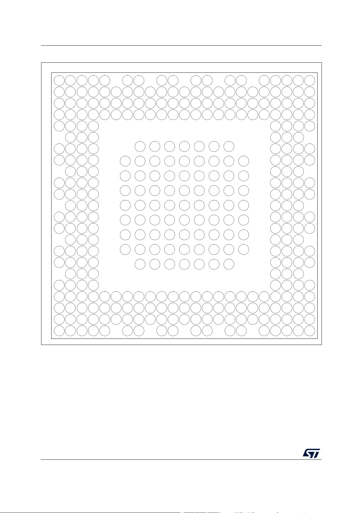
Pinouts, pin description and alternate functions STM32MP157C/F
MSv47430V3
PH15 PH12 PH4 PE12 PD10 PD4 PG15 PD0 PD1 PB9 PC7 PB15 PC6
DSI_
D0N
DSI_
CKP
PB4
DSI_
D1P
VDD_
DSINJTRST
PI0 PH10 PH14 PH11 PH9 PE14 VSS PE1 PE3 PE6 PE5 VSS
VDDA1
V8_DSI
DSI_
D0P
VSS_
DSI
PB14
VDD1
V2_DSI
_PHY
VDD1
V2_DSI
_REG
PA15
PH13 PD6 PE15 VSS PH8 PE0 PF5 PF0 PF4 PD7 PB7 PD2 PD3 PC10 PC11PC12 PC9 PC8 PE4
VSS PH5 PE13 PE11 PF1 PD5 PA 9 PG6 PB3 PF2
DSI_
CKN
PA8
DSI_
D1N
JTDO-
TRACE
SWO
VSS PG0 PA2 PF14 PB12 PC4 PA6 VSSPD11 PF8 PG7
USB_
DP2
PE8
USB_
DP1
OTG_
VBUS
DDR_
VREF
DDR_
DQ29
DDR_
DQ28
PE2 PC2 PB10
PA4
PF13 PG5 PG11 PB5
DDR_
DQ24
PF12 PF11 PH6 PF10 PB6 PE10 PB2PG9 PA10 PD12
DDR_
ATO
DDR_A8DDR_
DQ15
DDR_
DQ25
PG14 PG13 PH3 PA1 VSS PC1 PB1 VSS
DDR_
DQ30
PE9 PB13 PE7 VSS PF9
VDD
3V3_
USBHS
VSS_
USBHS
PF6
VDD
3V3_
USBFS
PA11 PD13
DDR_
DQM3
VSS
DDR_
DQ31
PB11 PG4 PA0 PH2 PC0 PB0 PC5 PA 7
DDR_
DQS3N
PG8 PB8 PG10 PF7
VDD
A1V8_
REG
VDD
A1V1_
REG
USB_
DM2
BYPAS
S_REG
1V8
USB_
DM1
USB_
RREF
PA12
DDR_
DQ27
DDR_
DQ26
DDR_
DQS3P
DDR_
DQ12
DDR_
DQ14
DDR_
DQ11
DDR_
A6
DDR_
DQ13
DDR_
DQ10
DDR_
DQ8
DDR_
CKE
DDR_
DQS1N
DDR_
DQS1P
DDR_
DQ9
DDR_
BA1
DDR_
DQM1
VSS
DDR_
A4
DDR_
A10
DDR_
A14
DDR_
A11
DDR_
CSN
DDR_
BA2
DDR_
WEN
DDR_
CLKN
DDR_
CLKP
DDR_
RASN
DDR_
CASN
DDR_
A12
DDR_
A1
VSS
DDR_
A15
DDR_
BA0
DDR_
ODT
DDR_
TO1
DDR_
A0
DDR_
DQM0
DDR_
DQ6
DDR_
DQ2
DDR_
A5
DDR_
DQ5
DDR_
DQ4
DDR_
A2
DDR_
ZQ
DDR_
A3
VSS
DDR_
DTO0
DDR_
DQ21
DDR_
DQ0
DDR_
DQ3
DDR_
A7
DDR_
DQ1
VSS
DDR_
A13
DDR_
DQS0N
DDR_
DQS0P
DDR_
DQ7
DDR_
A9
PG1 PC3 VSS PH7
PI10 PA14
PDR_
ON_
CORE
PG3
PF3 PA 3 ANA0 ANA1
PG2 PA5
PF15
PWR_ONPDR_
ON
VREF+
BOOT2 NRST
NRST_
CORE
BOOT0 PA13
PWR_
LP
BOOT1
PH0-
OSC_IN
PH1-
OSC_
OUT
VSS PI11
PC15-
OSC32
_OUT
PC14-
OSC32
_IN
PD14 PI8
PZ6 PZ5 VSS PI9
PD15 PZ7 PZ2
PD9 PC13 PD8 PG12
PI3 PI2 PI1 PI4
PI7 PI5 PI6
PZ1 PZ4 PZ0 PZ3
DDR_
DQS2N
JTCK-
SWCLK
DDR_
DQ19
DDR_
DQ16
DDR_
DQM2
JTMS-
SWDIO
VSS
DDR_
DQS2P
DDR_
DQ18
DDR_
RESET
N
DDR_
DQ22
DDR_
DQ17
VSSJTDI
DDR_
DQ20
DDR_
DQ23
VDD
CORE
VSS
VDD
CORE
VSS
VBAT
VSS_
ANA
VDDA
VDD
CORE
VSS
VDD
CORE
VSS
VDD
CORE
VSS
VDD_
ANA
VSSA
VDD
VSS
VDD
CORE
VSS
VDD
CORE
VSS
VDD
VSS
VDD
VSS
VDD
CORE
VSS
VDD
CORE
VSS
VDDCO
RE
VSS
VDD
VSS
VDD
VSS
VDD
CORE
VSS
VDD
CORE
VSS
VDD
CORE
VSS
VDD
VSS
VDD
CORE
VSS
VDD
CORE
VSS
VDD
CORE
VSS
VDD
CORE
VSS
VDD
VSS
VDDQ_
DDR
VSS
VDD
CORE
VSS
VDD
CORE
VSS
VDD
CORE
VSS
VDDQ_
DDR
VSS
VDDQ_
DDR
VSS
VDDQ_
DDR
VSS
VDDQ_
DDR
VSS
VDDQ_
DDR
VDDQ_
DDR
VSS
VDDQ_
DDR
VSS
VDDQ_
DDR
VSS
VDDQ_
DDR
192345678
1A
1B
1C
1D
1E
1F
1G
1H
1J
A
B
C
D
E
F
G
H
J
K
L
M
N
P
R
T
U
V
W
Y
AA
AB
AC
23143 22212014131211109876519181716152
Figure 7. STM32MP157C/FACxx TFBGA361 pinout
The above figure shows the package top view.
62/260 DS12505 Rev 5

STM32MP157C/F Pinouts, pin description and alternate functions
MSv47431V3
A
B
C
D
E
F
G
H
J
K
L
M
N
P
R
T
U
V
W
Y
AA
AB
PH10 VSS PH11 PE14 PK7 PK3 PJ14 PJ12 PF1 PD1 PD3 PB15
VDDA
1V8_
DSI
DSI_
D0P
DSI_
CKP
PA8
DSI_
D1P
VDD1V
2_DSI_
REG
VSS
DDR_
DQS2N
DDR_
DQ19
DDR_
DQ16
PH15 PH14 VSS PE15 PE0 PK5 PJ15 VSS PD4 PD0 VSS PE5
VSS_
DSI
VSS_
DSI
VSS_
DSI
PB4
VSS_
DSI
VSS_
DSI
VSS
DDR_
DQM2
VSS
DDR_
DQS2P
PI0 PI14 PH13 VSS PE11 PH8 PE1 PK0 PF5 PG15 PG6 PD2 PC9 PC11 JTDIPC7
JTCK-
SWCLK
VDD_
PLL2
VSS_
PLL2
DDR_
DQ18
DDR_
DQ22
DDR_
DQ17
VSS PH5 PH4 PE13 PK6 PK4 PJ13 PD10 PD5 PE3 PA9 PB3
VDD_
DSI
DSI_
D0N
DSI_
CKN
PB14
DSI_
D1N
VDD1
V2_DSI
_PHY
VSS VSS
DDR_
DQ20
DDR_
DQ23
PI7 PI5 PI15 PZ3 PH12 VSS VSS VSS PF4 PD7 PB7 PB9 PC10 PE4 VSSPF2
VDDQ_
DDR
DDR_
A7
DDR_
RESET
N
VSS
DDR_
DQ1
PZ4 PZ0 PZ6 VSS PI6 VSS VSS VSS VSS VSS
VDDQ_
DDR
VSS
DDR_
A13
DDR_
DQ7
DDR_
DQS0P
DDR_
DQM0
DDR_
DQS0N
PI13 PI12 PZ7 PZ5 PZ1 PJ8 VSS
VDD
CORE
VDD
CORE
VDD
CORE
VDD
CORE
VDDQ_
DDR
DDR_A9DDR_
A5
DDR_
DQ6
DDR_
DQ5
DDR_
DQ2
PI2 PI1 PI3 PE12 VSS PH9 PK1 PK2 PE6 PF0 PA15 PC12 PC8
NJTRS
T
JTDO-
TRACE
SWO
PC6
JTMSSWDIO
VDDQ_
DDR
VSS
DDR_
DQ21
DDR_
DQ3
DDR_
DQ0
PJ5 PJ4 VSS PJ2 PZ2 PJ11 VSS
VDD
CORE
VSS
VDD
CORE
VSS VSS
VDD
CORE
VDD
CORE
VDDQ_
DDR
DDR_
BA2
DDR_
A0
DDR_
ZQ
DDR_
BA0
DDR_
DTO1
PD15 PJ9 PD6 PJ7 PJ6 PJ1
VDD
CORE
VSS
VDD
CORE
VSS
VDD
CORE
VDD
CORE
VDDQ_
DDR
VSS VSS
DDR_
CSN
VSS
DDR_
DTO0
VSS
DDR_
ODT
PD8 PD9 PD14 VBAT
VSS_
PLL
VDD_
PLL
VSS VDD VSS
VDD
CORE
VSS VSS
VDD
CORE
VDD
CORE
VDDQ_
DDR
DDR_A1DDR_
A15
DDR_
CASN
DDR_
RASN
DDR_
WEN
PJ3 PJ0 PJ10 PG12 PI9 PI4
VDD
CORE
VSS
VDD
CORE
VSS
VDD
CORE
VDD
CORE
VDDQ_
DDR
VSS VSS
DDR_A2DDR_
A3
VSS
DDR_
DQ4
PC14-
OSC32
_IN
PC15-
OSC32
_OUT
VSS BOOT2
VSS_
ANA
VREF+ VSS VDD VSS VDD VSS VSS
VDD
CORE
VDD
CORE
VDDQ_
DDR
DDR_
A14
DDR_
A11
VSS
DDR_
DQ10
NRST_
CORE
NRST PA14 ANA0 VDDA VSSA VSS VDD VDD
VDD
CORE
VDDQ_
DDR
VSS
DDR_
BA1
DDR_
CKE
DDR_
DQS1N
DDR_
DQ13
DDR_
DQ9
PH0-
OSC_IN
PH1-
OSC_
OUT
PI11 PA 3 ANA1 VSSA VSS VSS VSS
VDD
CORE
VDD
VDDQ_
DDR
DDR_
A4
VSS
DDR_
DQS1P
DDR_
DQ11
DDR_
DQM1
PI8 PC13 BOOT0 BOOT1
VDD_
ANA
VREF- VDD VSS VDD VSS
VDD
CORE
VDD
CORE
VDDQ_
DDR
VSS VSS
DDR_
A10
DDR_
A12
DDR_
DQ8
DDR_
CLKP
DDR_
CLKN
PWR_ONPDR_
ON
PF3 PA1 VSS PA 4 PF14 PF12 PB10 PB13 PH6 PF10 PD13
OTG_
VBUS
VSSPB2
VDDQ_
DDR
VSS VSS
DDR_
DQ24
DDR_
DQ12
DDR_
DQ15
PI10 PH7 PA13 PG2 PG0 PF15 PF13 PF11 PA 6 PE7 PE9 PD12 PE10 PG9 PA12PB6 VSS
VDDQ_
DDR
VSS
DDR_
DQ30
DDR_
DQ25
DDR_
DQ31
PC2 PE2 VSS PG1 PB11 PH3 VSS PG8 PA 7 VSS PG7 PE8
VSS_
USBHS
VSS_
USBHS
PA11
VSS_
USBHS
PA10 VSS
VDDQ_
DDR
DDR_
DQS3N
VSS
DDR_
DQS3P
PWR_
LP
PDR_
ON_
CORE
PC3 PG3 PA 5 VSSA VSS PG5 VDD PC0 PG11 VDD VDD VSS
VDDQ_
DDR
VSS VSS
DDR_A8DDR_
A6
VSS
DDR_
DQ14
VSS PA2 PC1 PG4 PB0 PC4 PH2 PB8 PD11 PF8 PF9
VDDA
1V8_
REG
USB_
DP2
USB_
DM1
VDD
3V3_
USBFS
VDD
3V3_
USBHS
VDDA
1V1_
REG
VSS
DDR_
VREF
VSS
DDR_
DQ27
DDR_
DQ26
PG13 PG14 PA0 VSS PB1 PC5 PB12 PB5 PG10 PF7 PF6
BYPAS
S_REG
1V8
USB_
DM2
USB_
DP1
VSS_
USBHS
VSS_
USBHS
USB_
RREF
VSS
DDR_
ATO
DDR_
DQM3
DDR_
DQ29
DDR_
DQ28
22143 2120141312111098765 19181716152
Figure 8. STM32MP157C/FAAxx LFBGA448 pinout
The above figure shows the package top view.
DS12505 Rev 5 63/260
122

Pinouts, pin description and alternate functions STM32MP157C/F
Table 6. Legend/abbreviations used in the pinout table
Name Abbreviation Definition
Pin name
Unless otherwise specified, the pin function during and after reset is the same as the actual pin
name
S Supply pin
I Input only pin
Pin type
O Output only pin
I/O Input / output pin
A Analog or special level pin
FT(U/D/PD) 5 V tolerant I/O (with fixed pull-up / pull-down / programmable pull-down)
TT 3.6 V tolerant I/O directly connected to DAC
DDR 1.5 V, 1.35 V or 1.2 V I/O for DDR3, DDR3L, LPDDR2/LPDDR3 interface
DSI 1.2 V I/O for DSI interface
A Analog signal
RST Reset pin with weak pull-up resistor
I/O structure
_f
_a
_u
_h
_vh
(1)
(2)
(3)
(4)
(5)
I2C FM+ option
Analog option (supplied by VDDA for the analog part of the I/O)
USB option (supplied by VDD3V3_USBxx for the USB part of the I/O)
High-speed output for 1.8V typ. VDD (for SPI, SDMMC, QUADSPI, TRACE)
Very-high-speed option for 1.8V typ. VDD (for ETH, SPI, SDMMC, QUADSPI,
TRACE)
Option for TT or FT I/Os
Notes Unless otherwise specified by a note, all I/Os are set as floating inputs during and after reset
Alternate
functions
Additional
functions
1. The related I/O structures in Table 7 are: FT_f, FT_favh, FT_fh, FT_fha, FT_uf
2. The related I/O structures in Table 7 are: FT_a, TT_a, FT_avh, FT_favh, FT_fha, FT_ha, TT_ha
3. The related I/O structures in Table 7 are: FT_u, FT_uf
4. The related I/O structures in Table 7 are: FT_h, FT_fh, FT_fha, FT_ha, TT_ha
5. The related I/O structures in Table 7 are: FT_vh, FT_avh, FT_favh
Functions selected through GPIOx_AFR registers
Functions directly selected/enabled through peripheral registers
64/260 DS12505 Rev 5

STM32MP157C/F Pinouts, pin description and alternate functions
Pin Number
Table 7. STM32MP157C/F pin and ball definitions
Pin functions
Pin name
(function after
TFBGA257
LFBGA354
TFBGA361
reset)
LFBGA448
Pin type
I/O structure
- - A2 A2 PH5 I/O FT_f -
Notes
Alternate functions
I2C2_SDA, SPI5_NSS,
SAI4_SD_B, EVENTOUT
Additional
functions
TIM5_CH1, I2C4_SMBA,
- - C2 B1 PH10 I/O FT -
I2C1_SMBA, DCMI_D1, LCD_R4,
EVENTOUT
HDP2, TIM5_CH3, I2C4_SDA,
- - B2 F5 PH12 I/O FT_f -
I2C1_SDA, DCMI_D3, LCD_R6,
EVENTOUT
TIM8_CH1N, UART4_TX,
- - D1 D3 PH13 I/O FT -
FDCAN1_TX, LCD_G2,
EVENTOUT
1E2 K6 1F3 M9 VDD S - - - -
A1 A1 A1 A1 VSS S - - - -
TIM8_CH2N, UART4_RX,
- - C3 C2 PH14 I/O FT -
FDCAN1_RX, DCMI_D4,
LCD_G3, EVENTOUT
- - B1 C1 PH15 I/O FT -
TIM8_CH3N, DCMI_D11,
LCD_G4, EVENTOUT
TRACED14, TIM1_CH3N,
- - - H6 PJ8 I/O FT_h -
TIM8_CH1, UART8_TX,
LCD_G1, EVENTOUT
- - - D2 PI14 I/O FT_h -
TRACECLK, LCD_CLK,
EVENTOUT
- - - F3 PI15 I/O FT - LCD_G2, LCD_R0, EVENTOUT TIM5_CH4, SPI2_NSS/I2S2_WS,
- - C1 D1 PI0 I/O FT -
DCMI_D13, LCD_G5,
EVENTOUT
TIM8_BKIN2,
- - E3 E2 PI1 I/O FT_h -
SPI2_SCK/I2S2_CK, DCMI_D8,
LCD_G6, EVENTOUT
TIM8_CH4,
- - E2 E1 PI2 I/O FT_h -
SPI2_MISO/I2S2_SDI, DCMI_D9,
LCD_G7, EVENTOUT
1B3 E7 1A2 H9 VDDCORE S - - - -
TIM8_ETR,
- - E1 E3 PI3 I/O FT_h -
SPI2_MOSI/I2S2_SDO,
DCMI_D10, EVENTOUT
- - E4 J6 PI4 I/O FT -
TIM8_BKIN, SAI2_MCLK_A,
DCMI_D5, LCD_B4, EVENTOUT
TIM8_CH1, SAI2_SCK_A,
- - F3 F2 PI5 I/O FT -
DCMI_VSYNC, LCD_B5,
EVENTOUT
- - F4 G5 PI6 I/O FT -
TIM8_CH2, SAI2_SD_A,
DCMI_D6, LCD_B6, EVENTOUT
-
-
-
-
-
-
-
-
-
-
-
-
-
-
-
DS12505 Rev 5 65/260
122

Pinouts, pin description and alternate functions STM32MP157C/F
Table 7. STM32MP157C/F pin and ball definitions (continued)
Pin Number
Pin name
(function after
reset)
TFBGA257
LFBGA354
TFBGA361
- - F2 F1 PI7 I/O FT -
- A19 A23 A19 VSS S - - - -
- - G1 H5 PZ1 I/O FT_fh -
- - G4 F4 PZ3 I/O FT_f -
- - H4 J5 PI9 I/O FT -
- - G3 G2 PZ0 I/O FT_fh -
- - J4 K5 PZ2 I/O FT_fh -
- - G2 G1 PZ4 I/O FT_f -
G1 B2 - A22 VSS S - - - -
D1 F1 K4 J4 PG12 I/O FT_h -
- - H2 H4 PZ5 I/O FT_f -
- E9 - - VDDCORE S - - - -
- - H1 G3 PZ6 I/O FT_f -
- - J3 H3 PZ7 I/O FT_f -
LFBGA448
Pin type
Notes
I/O structure
Alternate functions
TIM8_CH3, SAI2_FS_A,
DCMI_D7, LCD_B7, EVENTOUT
I2C6_SDA, I2C2_SDA,
I2C5_SDA,
SPI1_MISO/I2S1_SDI,
I2C4_SDA, USART1_RX,
SPI6_MISO, EVENTOUT
I2C6_SDA, I2C2_SDA,
I2C5_SDA, SPI1_NSS/I2S1_WS,
I2C4_SDA,
USART1_CTS/USART1_NSS,
SPI6_NSS, EVENTOUT
HDP1, UART4_RX,
FDCAN1_RX, LCD_VSYNC,
EVENTOUT
I2C6_SCL, I2C2_SCL,
SPI1_SCK/I2S1_CK,
USART1_CK, SPI6_SCK,
EVENTOUT
I2C6_SCL, I2C2_SCL,
I2C5_SMBA,
SPI1_MOSI/I2S1_SDO,
I2C4_SMBA, USART1_TX,
SPI6_MOSI, EVENTOUT
I2C6_SCL, I2C2_SCL,
I2C5_SCL, I2C4_SCL,
EVENTOUT
LPTIM1_IN1, SPI6_MISO,
SAI4_CK2,
USART6_RTS/USART6_DE,
SPDIFRX_IN2, LCD_B4,
SAI4_SCK_A, ETH1_PHY_INTN,
FMC_NE4, LCD_B1, EVENTOUT
I2C6_SDA, I2C2_SDA,
I2C5_SDA, I2C4_SDA,
USART1_RTS/USART1_DE,
EVENTOUT
I2C6_SCL, I2C2_SCL,
USART1_CK, I2S1_MCK,
I2C4_SMBA, USART1_RX,
EVENTOUT
I2C6_SDA, I2C2_SDA,
USART1_TX, EVENTOUT
Pin functions
Additional
functions
-
-
-
-
-
-
-
-
-
-
-
66/260 DS12505 Rev 5

STM32MP157C/F Pinouts, pin description and alternate functions
Table 7. STM32MP157C/F pin and ball definitions (continued)
Pin Number
Pin name
(function after
TFBGA257
LFBGA354
TFBGA361
LFBGA448
reset)
Pin type
I/O structure
- - - H2 PI12 I/O FT_h -
Notes
Alternate functions
TRACED0, HDP0, LCD_HSYNC,
EVENTOUT
- B6 C7 B2 VSS S - - - -
- - - H1 PI13 I/O FT_h -
TRACED1, HDP1, LCD_VSYNC,
EVENTOUT
- - 1A4 H11 VDDCORE S - - - -
TIM1_CH2N, TIM8_CH2,
- - - J3 PJ10 I/O FT_h -
SPI5_MOSI, LCD_G3,
EVENTOUT
TIM1_CH2, TIM8_CH2N,
- - - K6 PJ11 I/O FT_h -
SPI5_MISO, LCD_G4,
EVENTOUT
- - - J2 PJ0 I/O FT_h -
TRACED8, LCD_R7, LCD_R1,
EVENTOUT
- - - L6 PJ1 I/O FT_h - TRACED9, LCD_R2, EVENTOUT -
- - - K4 PJ2 I/O FT_h -
TRACED10, DSI_TE, LCD_R3,
EVENTOUT
-L5 - - VDD S - - - -
- - - J1 PJ3 I/O FT_h -
TRACED11, LCD_R4,
EVENTOUT
N1 C3 - B19 VSS S - - - -
- - - K2 PJ4 I/O FT_h -
TRACED12, LCD_R5,
EVENTOUT
1D3 E11 - - VDDCORE S - - - -
- - - K1 PJ5 I/O FT_h -
- - - L5 PJ6 I/O FT_h -
- - - L4 PJ7 I/O FT_h -
TRACED2, HDP2, LCD_R6,
EVENTOUT
TRACED3, HDP3, TIM8_CH2,
LCD_R7, EVENTOUT
TRACED13, TIM8_CH2N,
LCD_G0, EVENTOUT
- C17 C12 C3 VSS S - - - -
TIM16_CH1N, SAI1_D1,
DFSDM1_CKIN4,
DFSDM1_DATIN1,
1B1 E3 D2 L3 PD6 I/O FT_ha -
SPI3_MOSI/I2S3_SDO,
SAI1_SD_A, USART2_RX,
FMC_NWAIT, DCMI_D10,
LCD_B2, EVENTOUT
- E13 - H13 VDDCORE S - - - -
TRACED15, TIM1_CH3,
- - - L2 PJ9 I/O FT_h -
TIM8_CH1N, UART8_RX,
LCD_G2, EVENTOUT
Pin functions
Additional
functions
-
-
-
-
-
-
-
-
-
-
-
-
-
DS12505 Rev 5 67/260
122

Pinouts, pin description and alternate functions STM32MP157C/F
Table 7. STM32MP157C/F pin and ball definitions (continued)
Pin Number
Pin name
TFBGA257
LFBGA354
TFBGA361
LFBGA448
(function after
reset)
Pin type
Notes
I/O structure
Alternate functions
- J5 - M6 VDD_PLL S - - - -
- J4 - M5 VSS_PLL S - - - -
TIM4_CH3, SAI3_MCLK_B,
1E1 F3 L3 M3 PD14 I/O FT_a -
UART8_CTS,
FMC_AD0/FMC_D0, EVENTOUT
TIM4_CH4, SAI3_MCLK_A,
1C2 G1 J2 L1 PD15 I/O FT_a -
FMC_AD1/FMC_D1, LCD_R1,
UART8_CTS,
EVENTOUT
DFSDM1_CKIN3, SAI3_SCK_B,
E1 F2 K3 M1 PD8 I/O FT_a -
USART3_TX, SPDIFRX_IN2,
FMC_AD13/FMC_D13, LCD_B7,
EVENTOUT
DFSDM1_DATIN3, SAI3_SD_B,
USART3_RX,
1C1 G3 K1 M2 PD9 I/O FT_a -
FMC_AD14/FMC_D14,
DCMI_HSYNC, LCD_B0,
EVENTOUT
-- - N8 VDD S -- - -
Pin functions
Additional
functions
-
-
-
-
W1 D1 C21 C8 VSS S - - - -
- - 1A6 - VDDCORE S - - - -
1D1 H3 1F1 M4 VBAT S - - - -
- D4 - C11 VSS S - - - -
RTC_OUT2/
RTC_LSCO,
TAMP_I N2/
- - L4 N1 PI8 I/O FT
(1)
EVENTOUT
TAMP_O UT3,
WKUP4
RTC_OUT1/
RTC_TS/
RTC_LSCO,
TAMP_I N1/
G3 K3 K2 N2 PC13 I/O FT
(1)
EVENTOUT
TAMP_O UT2/
TAMP_O UT3,
WKUP3
F3 D5 D4 C19 VSS S - - - -
F2 H2 L1 P2
PC15-
OSC32_OUT
I/O FT
(1)
EVENTOUT OSC32_OUT
- F4 - H15 VDDCORE S - - - -
1C4 F6 1B1 - VDDCORE S - - - -
G2 H1 L2 P1
PC14-
OSC32_IN
I/O FT
(1)
EVENTOUT OSC32_IN
68/260 DS12505 Rev 5

STM32MP157C/F Pinouts, pin description and alternate functions
Table 7. STM32MP157C/F pin and ball definitions (continued)
Pin Number
Pin name
TFBGA257
LFBGA354
TFBGA361
LFBGA448
(function after
reset)
Pin type
Notes
I/O structure
Alternate functions
E2 J1 M3 R2 NRST I/O RST - - -
J3 J2 M4 R1 NRST_CORE I RST - - -
H3 K1 N1 N3 BOOT0 I FTPD - - -
K3 K4 N4 N4 BOOT1 I FTPD - - -
H1 L2 M2 P4 BOOT2 I FTPD - - -
H2 M1 P1 T1 PH0-OSC_IN I/O FT - EVENTOUT OSC_IN
- - - J8 VDDCORE S - - - -
J2 M2 P2 T2
PH1-
OSC_OUT
I/O FT - EVENTOUT OSC_OUT
- D8 - C20 VSS S - - - -
M2 L1 R2 V1 PWR_ON O FT - - PWR_ONLP
K1 P1 N3 U1 PWR_LP O FT - - -
K2 N1 T3 U2
PDR_ON_
CORE
IFT- - -
L3 N2 R3 V2 PDR_ON I FT - - -
Pin functions
Additional
functions
- L3 1G2 N5 VDD_ANA S - - - -
- L4 1G1 P5 VSS_ANA S - - - -
L2 P2 N2 W3 PA13 I/O FT_a -
L1 R1 T2 R3 PA14 I/O FT_a -
- - P4 T3 PI11 I/O FT -
DBTRGO, DBTRGI, MCO1,
UART4_TX, EVENTOUT
DBTRGO, DBTRGI, MCO2,
EVENTOUT
MCO1, I2S_CKIN, LCD_G6,
EVENTOUT
BOOTFAILN
WKUP5
HDP0,
USART3_CTS/USART3_NSS,
- - T1 W1 PI10 I/O FT -
ETH1_GMII_RX_ER/
ETH1_MII_RX_ER,
LCD_HSYNC, EVENTOUT
-L71G4 - VDD S - - - -
W5 E2 F21 - VSS S - - - -
- F8 - - VDDCORE S - - - -
1F1 M4 1H1 R5 VDDA S - - - -
1F2 - - - VDDA S - - - -
M3 N3 R4 P6 VREF+ S - - - -
1G1 N4 1H2 R6 VSSA S - - - -
- P5 - T6 VSSA S - - - -
-
-
DS12505 Rev 5 69/260
122

Pinouts, pin description and alternate functions STM32MP157C/F
Table 7. STM32MP157C/F pin and ball definitions (continued)
Pin Number
Pin name
(function after
reset)
TFBGA257
LFBGA354
TFBGA361
- R5 - U6 VSSA S - - - -
-M3 - N6 VREF- S - - - -
- - W4 W2 PH7 I/O FT_fh -
- - U1 V3 PF3 I/O FT_vh -
P3 T3 W2 U3 PC3 I/O FT_ha -
- - T4 U4 PG3 I/O FT_vh -
P1 T1 Y1 Y2 PE2 I/O FT_favh -
-- -N10 VDD S -- - -
- E4 H3 D4 VSS S - - - -
N2 P3 U2 T4 PA3 I/O FT_a -
P2 T2 Y2 Y1 PC2 I/O FT_avh -
- - V2 W4 PG2 I/O FT_vh -
LFBGA448
Pin type
Notes
I/O structure
Alternate functions
I2C3_SCL, SPI5_MISO,
ETH1_GMII_RXD3/
ETH1_MII_RXD3/
ETH1_RGMII_RXD3,
MDIOS_MDC, DCMI_D9,
EVENTOUT
ETH1_GMII_TX_ER, FMC_A3,
EVENTOUT
TRACECLK, DFSDM1_DATIN1,
SPI2_MOSI/I2S2_SDO,
ETH1_GMII_TX_CLK/
ETH1_MII_TX_CLK, EVENTOUT
TRACED3, TIM8_BKIN2,
DFSDM1_CKIN1,
ETH1_GMII_TXD7, FMC_A13,
EVENTOUT
TRACECLK, SAI1_CK1,
I2C4_SCL, SPI4_SCK,
SAI1_MCLK_A,
QUADSPI_BK1_IO2,
ETH1_GMII_TXD3/
ETH1_MII_TXD3/
ETH1_RGMII_TXD3, FMC_A23,
EVENTOUT
TIM2_CH4, TIM5_CH4,
LPTIM5_OUT, TIM15_CH2,
USART2_RX, LCD_B2,
ETH1_GMII_COL/
ETH1_MII_COL, LCD_B5,
EVENTOUT
DFSDM1_CKIN1,
SPI2_MISO/I2S2_SDI,
DFSDM1_CKOUT,
ETH1_GMII_TXD2/
ETH1_MII_TXD2/
ETH1_RGMII_TXD2,
DCMI_PIXCLK, EVENTOUT
TRACED2, MCO2, TIM8_BKIN,
ETH1_GMII_TXD6, FMC_A12,
EVENTOUT
Pin functions
Additional
functions
-
-
ADC1_INP13,
ADC1_INN12
-
-
ADC1_INP15,
PVD_IN
ADC1_INP12,
ADC1_INN11
-
70/260 DS12505 Rev 5

STM32MP157C/F Pinouts, pin description and alternate functions
Table 7. STM32MP157C/F pin and ball definitions (continued)
Pin Number
Pin name
TFBGA257
LFBGA354
TFBGA361
LFBGA448
(function after
reset)
Pin type
Notes
I/O structure
Alternate functions
TRACED1, LPTIM1_ETR,
SPI6_MOSI, SAI4_D1,
USART6_TX,
QUADSPI_BK2_IO3,
R2 U1 AA1 AA2 PG14 I/O FT_vh -
SAI4_SD_A, ETH1_GMII_TXD1/
ETH1_MII_TXD1/
ETH1_RGMII_TXD1/
ETH1_RMII_TXD1, FMC_A25,
LCD_B0, EVENTOUT
- - W1 Y4 PG1 I/O FT_vh -
TRACED1, ETH1_GMII_TXD5,
FMC_A11, EVENTOUT
TRACED0, LPTIM1_OUT,
SAI1_CK2, SAI4_CK1,
SPI6_SCK, SAI1_SCK_A,
USART6_CTS/USART6_NSS,
R3 U2 AA2 AA1 PG13 I/O FT_vh -
SAI4_MCLK_A,
ETH1_GMII_TXD0/
ETH1_MII_TXD0/
ETH1_RGMII_TXD0/
ETH1_RMII_TXD0, FMC_A24,
LCD_R0, EVENTOUT
- - U3 R4 ANA0 A A - -
TIM2_CH1/TIM2_ETR,
TIM5_CH1, TIM8_ETR,
TIM15_BKIN,
N3 R3 AB3 AA3 PA0 I/O FT_ha -
USART2_CTS/USART2_NSS,
UART4_TX, SDMMC2_CMD,
SAI2_SD_B, ETH1_GMII_CRS/
ETH1_MII_CRS, EVENTOUT
- E5 - E5 VSS S - - - -
- - U4 T5 ANA1 A A - -
ETH_CLK, TIM2_CH2,
TIM5_CH2, LPTIM3_OUT,
TIM15_CH1N,
USART2_RTS/USART2_DE,
UART4_RX,
T1 U4 AA4 V4 PA1 I/O FT_ha -
QUADSPI_BK1_IO3,
SAI2_MCLK_B,
ETH1_GMII_RX_CLK/
ETH1_MII_RX_CLK/
ETH1_RGMII_RX_CLK/
ETH1_RMII_REF_CLK, LCD_R2,
EVENTOUT
Pin functions
Additional
functions
-
-
-
ADC1_INP0,
ADC1_INN1,
ADC2_INP0,
ADC2_INN1
ADC1_INP16,
WKUP1
ADC1_INP1,
ADC2_INP1
ADC1_INP17,
ADC1_INN16
DS12505 Rev 5 71/260
122

Pinouts, pin description and alternate functions STM32MP157C/F
Table 7. STM32MP157C/F pin and ball definitions (continued)
Pin Number
Pin name
(function after
reset)
TFBGA257
LFBGA354
TFBGA361
1H1 P4 V3 U5 PA5 I/O TT_ha -
1J1 R4 V4 V6 PA4 I/O TT_a -
- - AC2 W5 PG0 I/O FT_vh -
U3 V1 AB1 Y5 PB11 I/O FT_favh -
- - AB2 AB4 PG4 I/O FT_vh -
T3 W2 AC3 AB2 PA2 I/O FT_ha -
1F3 M6 - - VDD S - - - -
T2 V2 AA6 AB3 PC1 I/O FT_ha -
A6 - K21 E19 VSS S - - - -
- - Y6 U8 PG5 I/O FT -
- F10 1B3 J10 VDDCORE S - - - -
LFBGA448
Pin type
Notes
I/O structure
Alternate functions
TIM2_CH1/TIM2_ETR,
TIM8_CH1N, SAI4_CK1,
SPI1_SCK/I2S1_CK, SPI6_SCK,
SAI4_MCLK_A, LCD_R4,
EVENTOUT
HDP0, TIM5_ETR, SAI4_D2,
SPI1_NSS/I2S1_WS,
SPI3_NSS/I2S3_WS,
USART2_CK, SPI6_NSS,
SAI4_FS_A, DCMI_HSYNC,
LCD_VSYNC, EVENTOUT
TRACED0, DFSDM1_DATIN0,
ETH1_GMII_TXD4, FMC_A10,
EVENTOUT
TIM2_CH4, LPTIM2_ETR,
I2C2_SDA, DFSDM1_CKIN7,
USART3_RX,
ETH1_GMII_TX_EN/
ETH1_MII_TX_EN/
ETH1_RGMII_TX_CTL/
ETH1_RMII_TX_EN, DSI_TE,
LCD_G5, EVENTOUT
TIM1_BKIN2,
ETH1_GMII_GTX_CLK/
ETH1_RGMII_GTX_CLK,
FMC_A14, EVENTOUT
TIM2_CH3, TIM5_CH3,
LPTIM4_OUT, TIM15_CH1,
USART2_TX, SAI2_SCK_B,
SDMMC2_D0DIR, ETH1_MDIO,
MDIOS_MDIO, LCD_R1,
EVENTOUT
TRACED0, SAI1_D1,
DFSDM1_DATIN0,
DFSDM1_CKIN4,
SPI2_MOSI/I2S2_SDO,
SAI1_SD_A, SDMMC2_CK,
ETH1_MDC, MDIOS_MDC,
EVENTOUT
TIM1_ETR,
ETH1_GMII_CLK125/
ETH1_RGMII_CLK125,
FMC_A15, EVENTOUT
Pin functions
Additional
functions
ADC1_INP19,
ADC1_INN18,
ADC2_INP19,
ADC2_INN18,
DAC_OUT2
ADC1_INP18,
ADC2_INP18,
DAC_OUT1
-
-
-
ADC1_INP14,
WKUP2
ADC1_INP11,
ADC1_INN10,
ADC2_INP11,
ADC2_INN10,
TAMP_I N3,
WKUP6
-
72/260 DS12505 Rev 5

STM32MP157C/F Pinouts, pin description and alternate functions
Table 7. STM32MP157C/F pin and ball definitions (continued)
Pin Number
Pin name
TFBGA257
LFBGA354
TFBGA361
LFBGA448
(function after
reset)
Pin type
Notes
I/O structure
Alternate functions
DFSDM1_CKIN4,
QUADSPI_BK2_IO1,
- - AA3 Y6 PH3 I/O FT_h -
SAI2_MCLK_B,
ETH1_GMII_COL/
ETH1_MII_COL, LCD_R1,
EVENTOUT
TIM1_CH2N, TIM3_CH3,
TIM8_CH2N, DFSDM1_CKOUT,
UART4_CTS, LCD_R3,
U2 W3 AB6 AB5 PB0 I/O FT_a -
ETH1_GMII_RXD2/
ETH1_MII_RXD2/
ETH1_RGMII_RXD2,
MDIOS_MDIO, LCD_G1,
EVENTOUT
TRACED7, I2C4_SDA,
- - Y4 W6 PF15 I/O FT_fh -
I2C1_SDA, ETH1_GMII_RXD7,
FMC_A9, EVENTOUT
TIM1_CH3N, TIM3_CH4,
TIM8_CH3N, DFSDM1_DATIN1,
LCD_R6, ETH1_GMII_RXD3/
U1 V3 AA7 AA5 PB1 I/O FT_a -
ETH1_MII_RXD3/
ETH1_RGMII_RXD3,
MDIOS_MDC, LCD_G0,
EVENTOUT
- E6 - F6 VSS S - - - TRACED6, DFSDM1_CKIN6,
- - AC4 V7 PF14 I/O FT_fha -
I2C4_SCL, I2C1_SCL,
ETH1_GMII_RXD6, FMC_A8,
EVENTOUT
TRACED5, DFSDM1_DATIN6,
I2C4_SMBA, I2C1_SMBA,
- - Y5 W7 PF13 I/O FT_ha -
DFSDM1_DATIN3,
ETH1_GMII_RXD5, FMC_A7,
EVENTOUT
LPTIM1_IN2,
QUADSPI_BK2_IO0,
- - AB4 AB7 PH2 I/O FT_h -
SAI2_SCK_B, ETH1_GMII_CRS/
ETH1_MII_CRS, LCD_R0,
EVENTOUT
SAI1_D3, DFSDM1_DATIN2,
SAI4_D4, SAI1_D4,
SPDIFRX_IN4,
V1 V4 AB7 AA6 PC5 I/O FT_a -
ETH1_GMII_RXD1/
ETH1_MII_RXD1/
ETH1_RGMII_RXD1/
ETH1_RMII_RXD1, SAI4_D3,
EVENTOUT
Pin functions
Additional
functions
-
ADC1_INP9,
ADC1_INN5,
ADC2_INP9,
ADC2_INN5
-
ADC1_INP5,
ADC2_INP5
ADC2_INP6,
ADC2_INN2
ADC2_INP2
-
ADC1_INP8,
ADC1_INN4,
ADC2_INP8,
ADC2_INN4
DS12505 Rev 5 73/260
122

Pinouts, pin description and alternate functions STM32MP157C/F
Table 7. STM32MP157C/F pin and ball definitions (continued)
Pin Number
Pin name
(function after
reset)
TFBGA257
LFBGA354
TFBGA361
V2 W4 AC7 AB6 PC4 I/O FT_a -
- M8 - P9 VDD S - - - -
1D2 E8 P3 F7 VSS S - - - -
1J3 R7 1J2 U9 VDD S - - - -
- - Y9 V8 PF12 I/O FT_ha -
1E4 - - - VDDCORE S - - - -
W4 U5 Y10 W8 PF11 I/O FT_ha -
- E10 - F8 VSS S - - - -
W2 T6 AB8 Y9 PA7 I/O FT_ha -
- F12 - J12 VDDCORE S - - - -
W3 T5 AC8 W9 PA6 I/O FT_ha -
--1H3- VDD S -- - -
U4 T7 AB5 U10 PC0 I/O FT_ha -
1G2 E12 P21 F16 VSS S - - - -
LFBGA448
Pin type
Notes
I/O structure
Alternate functions
DFSDM1_CKIN2, I2S1_MCK,
SPDIFRX_IN3,
ETH1_GMII_RXD0/
ETH1_MII_RXD0/
ETH1_RGMII_RXD0/
ETH1_RMII_RXD0, EVENTOUT
TRACED4, ETH1_GMII_RXD4,
FMC_A6, EVENTOUT
SPI5_MOSI, SAI2_SD_B,
DCMI_D12, LCD_G5,
EVENTOUT
TIM1_CH1N, TIM3_CH2,
TIM8_CH1N, SAI4_D1,
SPI1_MOSI/I2S1_SDO,
SPI6_MOSI, TIM14_CH1,
QUADSPI_CLK,
ETH1_GMII_RX_DV/
ETH1_MII_RX_DV/
ETH1_RGMII_RX_CTL/
ETH1_RMII_CRS_DV,
SAI4_SD_A, EVENTOUT
TIM1_BKIN, TIM3_CH1,
TIM8_BKIN, SAI4_CK2,
SPI1_MISO/I2S1_SDI,
SPI6_MISO, TIM13_CH1,
MDIOS_MDC, SAI4_SCK_A,
DCMI_PIXCLK, LCD_G2,
EVENTOUT
DFSDM1_CKIN0, LPTIM2_IN2,
DFSDM1_DATIN4, SAI2_FS_B,
QUADSPI_BK2_NCS, LCD_R5,
EVENTOUT
Pin functions
Additional
functions
ADC1_INP4,
ADC2_INP4
ADC1_INP6,
ADC1_INN2
ADC1_INP2
ADC1_INP7,
ADC1_INN3,
ADC2_INP7,
ADC2_INN3
ADC1_INP3,
ADC2_INP3
ADC1_INP10,
ADC2_INP10
74/260 DS12505 Rev 5

STM32MP157C/F Pinouts, pin description and alternate functions
Table 7. STM32MP157C/F pin and ball definitions (continued)
Pin Number
Pin name
TFBGA257
LFBGA354
TFBGA361
LFBGA448
(function after
reset)
Pin type
Notes
I/O structure
Alternate functions
TIM2_CH3, LPTIM2_IN1,
I2C2_SCL, SPI2_SCK/I2S2_CK,
DFSDM1_DATIN7, USART3_TX,
U5 W5 Y3 V9 PB10 I/O FT_fha -
QUADSPI_BK1_NCS,
ETH1_GMII_RX_ER/
ETH1_MII_RX_ER, LCD_G4,
EVENTOUT
- - 1B5 - VDDCORE S - - - -
TIM1_BKIN, I2C6_SMBA,
I2C2_SMBA,
SPI2_NSS/I2S2_WS,
DFSDM1_DATIN1, USART3_CK,
V3 V5 AC5 AA7 PB12 I/O FT_avh -
USART3_RX, FDCAN2_RX,
ETH1_GMII_TXD0/
ETH1_MII_TXD0/
ETH1_RGMII_TXD0/
ETH1_RMII_TXD0, UART5_RX,
EVENTOUT
- G5 - J14 VDDCORE S - - - -
TIM1_CH1N, DFSDM1_CKOUT,
LPTIM2_OUT,
SPI2_SCK/I2S2_CK,
DFSDM1_CKIN1,
1J2 T9 AA10 V10 PB13 I/O FT_vh -
USART3_CTS/USART3_NSS,
FDCAN2_TX, ETH1_GMII_TXD1/
ETH1_MII_TXD1/
ETH1_RGMII_TXD1/
ETH1_RMII_TXD1, UART5_TX,
EVENTOUT
- E14 V21 F20 VSS S - - - -
ETH_CLK, TIM17_BKIN,
TIM3_CH2, SAI4_D1,
I2C1_SMBA,
SPI1_MOSI/I2S1_SDO,
V5 T8 Y8 AA8 PB5 I/O FT_vh -
I2C4_SMBA,
SPI3_MOSI/I2S3_SDO,
SPI6_MOSI, FDCAN2_RX,
SAI4_SD_A, ETH1_PPS_OUT,
UART5_RX, DCMI_D10,
LCD_G7, EVENTOUT
TRACED11, USART1_TX,
UART4_TX, SPDIFRX_IN1,
ETH1_GMII_TX_EN/
U6 V6 Y7 U11 PG11 I/O FT_vh -
ETH1_MII_TX_EN/
ETH1_RGMII_TX_CTL/
ETH1_RMII_TX_EN, DCMI_D3,
LCD_B3, EVENTOUT
Pin functions
Additional
functions
-
-
-
-
-
DS12505 Rev 5 75/260
122

Pinouts, pin description and alternate functions STM32MP157C/F
Table 7. STM32MP157C/F pin and ball definitions (continued)
Pin Number
Pin name
(function after
reset)
TFBGA257
LFBGA354
TFBGA361
1B5 G7 1C2 - VDDCORE S - - - -
- - Y11 V11 PH6 I/O FT_h -
1H2 E16 - G4 VSS S - - - -
V4 W6 AB10 AB8 PB8 I/O FT_favh -
- - - K9 VDDCORE S - - - -
V6 U7 AB9 Y8 PG8 I/O FT_vh -
-N5 - P11 VDD S - - - -
U7 V7 AB11 AA9 PG10 I/O FT_h -
- F5 W3 - VSS S - - - -
1J4 W7 AA9 W11 PE9 I/O FT_ha -
- G9 - - VDDCORE S - - - -
V7 T10 AA11 W10 PE7 I/O FT_h -
1C3 F7 - G6 VSS S - - - -
LFBGA448
Pin type
Notes
I/O structure
Alternate functions
TIM12_CH1, I2C2_SMBA,
SPI5_SCK, ETH1_GMII_RXD2/
ETH1_MII_RXD2/
ETH1_RGMII_RXD2,
MDIOS_MDIO, DCMI_D8,
EVENTOUT
HDP6, TIM16_CH1, TIM4_CH3,
DFSDM1_CKIN7, I2C1_SCL,
SDMMC1_CKIN, I2C4_SCL,
SDMMC2_CKIN, UART4_RX,
FDCAN1_RX, SDMMC2_D4,
ETH1_GMII_TXD3/
ETH1_MII_TXD3/
ETH1_RGMII_TXD3,
SDMMC1_D4, DCMI_D6,
LCD_B6, EVENTOUT
TRACED15,
TIM2_CH1/TIM2_ETR,
ETH_CLK, TIM8_ETR,
SPI6_NSS, SAI4_D2,
USART6_RTS/USART6_DE,
USART3_RTS/USART3_DE,
SPDIFRX_IN3, SAI4_FS_A,
ETH1_PPS_OUT, LCD_G7,
EVENTOUT
TRACED10, UART8_CTS,
LCD_G3, SAI2_SD_B,
QUADSPI_BK2_IO2, FMC_NE3,
DCMI_D2, LCD_B2, EVENTOUT
TIM1_CH1, DFSDM1_CKOUT,
UART7_RTS/UART7_DE,
QUADSPI_BK2_IO2,
FMC_AD6/FMC_D6, EVENTOUT
TIM1_ETR, TIM3_ETR,
DFSDM1_DATIN2, UART7_RX,
QUADSPI_BK2_IO0,
FMC_AD4/FMC_D4, EVENTOUT
Pin functions
Additional
functions
-
-
-
-
-
-
76/260 DS12505 Rev 5

STM32MP157C/F Pinouts, pin description and alternate functions
Table 7. STM32MP157C/F pin and ball definitions (continued)
Pin Number
Pin name
TFBGA257
LFBGA354
TFBGA361
LFBGA448
(function after
reset)
Pin type
Notes
I/O structure
Alternate functions
LPTIM2_IN2, I2C4_SMBA,
I2C1_SMBA,
USART3_CTS/USART3_NSS,
U8 V8 AC10 AB9 PD11 I/O FT_h -
QUADSPI_BK1_IO0,
SAI2_SD_A,
FMC_A16/FMC_CLE,
EVENTOUT
1D5 G11 1C4 - VDDCORE S - - - -
TIM17_CH1, SPI5_SCK,
W7 W8 AB12 AA10 PF7 I/O FT_ha -
SAI1_MCLK_B, UART7_TX,
QUADSPI_BK1_IO2, EVENTOUT
TRACED12, TIM16_CH1N,
SPI5_MISO, SAI1_SCK_B,
V8 U10 AC11 AB10 PF8 I/O FT_ha -
UART7_RTS/UART7_DE,
TIM13_CH1,
QUADSPI_BK1_IO0, EVENTOUT
- - - K11 VDDCORE S - - - TIM16_BKIN, SAI1_D3, SAI4_D4,
1J7 U9 Y12 V12 PF10 I/O FT_h -
SAI1_D4, QUADSPI_CLK,
SAI4_D3, DCMI_D11, LCD_DE,
EVENTOUT
- F9 AA5 G8 VSS S - - - -
TIM16_CH1, SPI5_NSS,
U10 V9 AA13 AA11 PF6 I/O FT_ha -
SAI1_SD_B, UART7_RX,
QUADSPI_BK1_IO3,
SAI4_SCK_B, EVENTOUT
- H4 - - VDDCORE S - - - -
LPTIM1_IN1, TIM4_CH1,
LPTIM2_IN1, I2C4_SCL,
U14 U11 Y18 W12 PD12 I/O FT_fha -
USART3_RTS/USART3_DE,
QUADSPI_BK1_IO1,
SAI2_FS_A,
FMC_A17/FMC_ALE,
EVENTOUT
- F11 AA8 G10 VSS S - - - -
TRACED13, TIM17_CH1N,
V9 W9 AA14 AB11 PF9 I/O FT_ha -
SPI5_MOSI, SAI1_FS_B,
UART7_CTS, TIM14_CH1,
QUADSPI_BK1_IO1, EVENTOUT
- H6 1C6 K13 VDDCORE S - - - -
Pin functions
Additional
functions
-
-
-
-
-
I2C1_SCL,
-
-
DS12505 Rev 5 77/260
122

Pinouts, pin description and alternate functions STM32MP157C/F
Table 7. STM32MP157C/F pin and ball definitions (continued)
Pin Number
Pin name
(function after
reset)
TFBGA257
LFBGA354
TFBGA361
V11 W10 AC14 Y11 PG7 I/O FT_h -
1E3 F15 - G12 VSS S - - - -
1F5 - - - VDDCORE S - - - -
W11 T12 Y14 W13 PB6 I/O FT_fha -
U12 T11 AC13 Y12 PE8 I/O FT_h -
V12 V10 Y15 W14 PE10 I/O FT_ha -
- H8 1D1 K15 VDDCORE S - - - -
V13 T13 Y16 V13 PB2 I/O FT_ha -
- H10 - - VDDCORE S - - - -
U13 U12 AA19 V14 PD13 I/O FT_fha -
-N7 - - VDD S - - - -
- G2 AA12 G14 VSS S - - - -
LFBGA448
Pin type
Notes
I/O structure
Alternate functions
TRACED5, SAI1_MCLK_A,
USART6_CK,
UART8_RTS/UART8_DE,
QUADSPI_CLK,
QUADSPI_BK2_IO3, DCMI_D13,
LCD_CLK, EVENTOUT
TIM16_CH1N, TIM4_CH1,
I2C1_SCL, CEC, I2C4_SCL,
USART1_TX, FDCAN2_TX,
QUADSPI_BK1_NCS,
DFSDM1_DATIN5, UART5_TX,
DCMI_D5, EVENTOUT
TIM1_CH1N, DFSDM1_CKIN2,
UART7_TX, QUADSPI_BK2_IO1,
FMC_AD5/FMC_D5, EVENTOUT
TIM1_CH2N, DFSDM1_DATIN4,
UART7_CTS,
QUADSPI_BK2_IO3,
FMC_AD7/FMC_D7, EVENTOUT
TRACED4, RTC_OUT2,
SAI1_D1, DFSDM1_CKIN1,
USART1_RX, I2S_CKIN,
SAI1_SD_A,
SPI3_MOSI/I2S3_SDO,
UART4_RX, QUADSPI_CLK,
EVENTOUT
LPTIM1_OUT, TIM4_CH2,
I2C4_SDA, I2C1_SDA,
I2S3_MCK, QUADSPI_BK1_IO3,
SAI2_SCK_A, FMC_A18,
DSI_TE, EVENTOUT
Pin functions
Additional
functions
-
-
-
-
-
-
1J8 V16 AB18 AA17 USB_RREF A A - - -
- W12 AA15 AB13
1H7 - - -
V10 W13 AC16 AB14 USB_DP2 A FT_u - -
78/260 DS12505 Rev 5
VDD3V3_
USBHS
VDD3V3_
USB
S-- - -
S-- - -
USBH_HS_DP2,
OTG_HS_DP

STM32MP157C/F Pinouts, pin description and alternate functions
Table 7. STM32MP157C/F pin and ball definitions (continued)
Pin Number
Pin name
TFBGA257
LFBGA354
TFBGA361
LFBGA448
(function after
reset)
Pin type
Notes
I/O structure
Alternate functions
W10 V13 AB16 AA14 USB_DM2 A FT_u - -
- U13 AA16 Y13 VSS_USBHS S - - - -
- - - Y14 VSS_USBHS S - - - -
U11 T15 AB13 AA12
BYPASS_
REG1V8
IFT- - -
DBTRGO, USART6_RX,
SPDIFRX_IN4,
QUADSPI_BK2_IO2,
W8 T14 Y13 W15 PG9 I/O FT_h -
SAI2_FS_B,
FMC_NE2/FMC_NCE,
DCMI_VSYNC, LCD_R1,
EVENTOUT
1G3 - 1H5 R10 VDD S - - - -
Pin functions
Additional
functions
USBH_HS_DM2,
OTG_HS_DM
-
-N9 - - VDD S - - - -
1H5 V11 AB14 AB12
VDDA1V8_
REG
S-- - -
1H3 - - G17 VSS S - - - -
1J6 W11 AB15 AB17
VDDA1V1_
REG
S-- - -
- G4 AA21 H7 VSS S - - - -
-- -R12 VDD S -- - -
-P6 - - VDD S - - - -
- U14 - Y15 VSS_USBHS S - - - -
- V12 - AA13 VSS_USBHS S - - - -
1D4 G6 AC1 J9 VSS S - - - -
- V15 - AA16 VSS_USBHS S - - - -
W14 W14 AB17 AB15 USB_DM1 A FT_u - - USBH_HS_DM1
V14 V14 AC17 AA15 USB_DP1 A FT_u - - USBH_HS_DP1
TIM1_ETR, I2C6_SDA,
I2C5_SDA, UART4_TX,
V15 U16 AB19 W16 PA12 I/O FT_uf -
USART1_RTS/USART1_DE,
OTG_FS_DP
SAI2_FS_B, FDCAN1_TX,
LCD_R5, EVENTOUT
- G8 - J11 VSS S - - - -
- - - L8 VDDCORE S - - - -
DS12505 Rev 5 79/260
122

Pinouts, pin description and alternate functions STM32MP157C/F
Table 7. STM32MP157C/F pin and ball definitions (continued)
Pin Number
Pin name
(function after
reset)
TFBGA257
LFBGA354
TFBGA361
U15 V17 AA18 Y16 PA11 I/O FT_uf -
1C6 H12 1D3 - VDDCORE S - - - -
1F4 G10 AC23 - VSS S - - - -
- W15 AA17 AB16
V16 U15 AC19 V15 OTG_VBUS A FT_u - -
U16 T16 Y17 Y17 PA10 I/O FT_u -
- - AB20 AB20 DDR_DQ27 I/O DDR - - -
1B9 E15 1A8 E18 VDDQ_DDR S - - - -
- - AB21 AB21 DDR_DQ26 I/O DDR - - -
LFBGA448
VDD3V3_
USBFS
Pin type
S-- - -
Notes
I/O structure
Alternate functions
TIM1_CH4, I2C6_SCL,
I2C5_SCL, SPI2_NSS/I2S2_WS,
UART4_RX,
USART1_CTS/USART1_NSS,
FDCAN1_RX, LCD_R4,
EVENTOUT
TIM1_CH3, SPI3_NSS/I2S3_WS,
USART1_RX, MDIOS_MDIO,
SAI4_FS_B, DCMI_D1, LCD_B1,
EVENTOUT
Pin functions
Additional
functions
OTG_FS_DM
OTG_FS_VBUS,
OTG_HS_VBUS
OTG_FS_ID,
OTG_HS_ID
- G12 - J13 VSS S - - - -
- - AC22 AA21 DDR_DQ28 I/O DDR - - -
1H4 G14 1A3 J17 VSS S - - - -
- - AC21 AA20 DDR_DQ29 I/O DDR - - -
- - Y22 W20 DDR_DQ25 I/O DDR - - -
- - AB22 Y21 DDR_DQS3P I/O DDR - - -
- H5 - J20 VSS S - - - -
- - AB23 Y22 DDR_DQS3N I/O DDR - - -
- - - F17 VDDQ_DDR S - - - -
- - AA20 AA22 DDR_DQM3 O DDR - - -
- F14 1B7 - VDDQ_DDR S - - - -
- - AA22 W21 DDR_DQ31 I/O DDR - - -
- H7 1A5 K3 VSS S - - - -
- - AA23 W22 DDR_DQ30 I/O DDR - - -
U9 H9 1A7 K7 VSS S - - - -
- - Y23 V22 DDR_DQ24 I/O DDR - - -
- - - G16 VDDQ_DDR S - - - -
80/260 DS12505 Rev 5

STM32MP157C/F Pinouts, pin description and alternate functions
Table 7. STM32MP157C/F pin and ball definitions (continued)
Pin Number
Pin name
TFBGA257
LFBGA354
TFBGA361
LFBGA448
(function after
reset)
Pin type
Notes
I/O structure
Alternate functions
- - - L10 VDDCORE S - - - -
W16 W16 AC20 AB19 DDR_VREF A A - - -
- H11 - K10 VSS S - - - -
W17 W18 W23 V20 DDR_DQ12 I/O DDR - - -
1C5 H13 1B2 K12 VSS S - - - -
V17 W17 Y21 V21 DDR_DQ15 I/O DDR - - -
- H15 - K14 VSS S - - - -
U17 V18 W22 U21 DDR_DQ14 I/O DDR - - -
W18 V19 W21 T20 DDR_DQ11 I/O DDR - - -
- G15 1B9 H17 VDDQ_DDR S - - - -
V19 U19 U22 T22 DDR_DQS1P I/O DDR - - -
Pin functions
Additional
functions
1E5 - 1B4 L9 VSS S - - - -
U18 T19 U23 R22 DDR_DQS1N I/O DDR - - -
V18 U18 V22 T21 DDR_DQM1 O DDR - - -
1D9 - - J16 VDDQ_DDR S - - - -
T18 T18 T23 R20 DDR_DQ13 I/O DDR - - -
- J3 1B6 - VSS S - - - -
U19 T17 U21 R21 DDR_DQ9 I/O DDR - - -
1G5 J6 - L11 VSS S - - - -
T19 R18 T22 P21 DDR_DQ10 I/O DDR - - -
- H14 - - VDDQ_DDR S - - - -
R18 P18 T21 N22 DDR_DQ8 I/O DDR - - -
- J8 1B8 L13 VSS S - - - -
1J5 J10 - L17 VSS S - - - -
1F8 N19 Y19 AA19 DDR_ATO A A - - -
- J7 - - VDDCORE S - - - -
- - 1C8 - VDDQ_DDR S - - - -
1G9 N16 W20 U19 DDR_A6 O DDR - - -
- - - K17 VDDQ_DDR S - - - -
T17 R17 Y20 U18 DDR_A8 O DDR - - -
- J12 1C1 L19 VSS S - - - -
R17 P17 V20 T18 DDR_A4 O DDR - - -
DS12505 Rev 5 81/260
122

Pinouts, pin description and alternate functions STM32MP157C/F
Table 7. STM32MP157C/F pin and ball definitions (continued)
Pin Number
Pin name
(function after
reset)
TFBGA257
LFBGA354
TFBGA361
1A6 J14 1C3 L20 VSS S - - - -
P17 P19 T20 R19 DDR_CKE O DDR - - -
P18 N17 U20 R18 DDR_BA1 O DDR - - -
- J15 - L16 VDDQ_DDR S - - - -
N18 N18 R21 P18 DDR_A14 O DDR - - -
- K2 - M7 VSS S - - - -
N19 M18 R20 P19 DDR_A11 O DDR - - -
- K5 1C5 M10 VSS S - - - -
1D6 K7 - M12 VSS S - - - -
M17 M19 R22 N18 DDR_A10 O DDR - - -
- J9 1D5 L12 VDDCORE S - - - -
LFBGA448
Pin type
Notes
I/O structure
Alternate functions
Pin functions
Additional
functions
- - 1D9 - VDDQ_DDR S - - - -
M18 L17 P23 N19 DDR_A12 O DDR - - -
M19 M17 P22 M18 DDR_A1 O DDR - - -
- K9 1C7 M14 VSS S - - - -
J19 K17 N20 M22 DDR_CASN O DDR - - -
1F6 K11 - N9 VSS S - - - -
J18 J17 M20 M21 DDR_WEN O DDR - - -
- K14 - M17 VDDQ_DDR S - - - -
1E9 L18 N21 M20 DDR_RASN O DDR - - -
L17 L19 N22 N20 DDR_CLKP O DDR - - -
- K13 1C9 - VSS S - - - -
K18 K19 N23 N21 DDR_CLKN O DDR - - -
1F9 - 1E8 N16 VDDQ_DDR S - - - -
1D8 K18 K20 L22 DDR_DTO0 O DDR - - -
1C8 J19 L21 K21 DDR_DTO1 O DDR - - -
L18 L16 P20 M19 DDR_A15 O DDR - - -
1H6 - 1D2 N11 VSS S - - - -
1E6 - - - VDDCORE S - - - -
- K15 - N13 VSS S - - - -
J17 J18 M22 L18 DDR_CSN O DDR - - -
H18 H19 L22 L21 DDR_ODT O DDR - - -
82/260 DS12505 Rev 5

STM32MP157C/F Pinouts, pin description and alternate functions
Table 7. STM32MP157C/F pin and ball definitions (continued)
Pin Number
Pin name
TFBGA257
LFBGA354
TFBGA361
LFBGA448
(function after
reset)
Pin type
Notes
I/O structure
Alternate functions
H17 J16 M21 K18 DDR_BA2 O DDR - - -
1C7 L6 1D4 N17 VSS S - - - -
G18 H18 L20 K19 DDR_A0 O DDR - - -
- L15 - P17 VDDQ_DDR S - - - -
G19 G19 L23 K20 DDR_BA0 O DDR - - -
E17 F17 F20 G18 DDR_A13 O DDR - - -
- L8 - P3 VSS S - - - -
F17 G18 J20 J18 DDR_A2 O DDR - - -
1E7 L10 1D6 P7 VSS S - - - -
F19 F19 K22 J19 DDR_A3 O DDR - - -
- - 1F9 - VDDQ_DDR S - - - -
C16 G16 D20 F19
DDR_
RESETN
ODDR- - -
- M14 - R16 VDDQ_DDR S - - - -
1C9 H17 H20 H19 DDR_A5 O DDR - - -
- L12 1D8 P10 VSS S - - - -
Pin functions
Additional
functions
1A9 E17 E20 F18 DDR_A7 O DDR - - -
- L14 - P12 VSS S - - - -
1A8 F18 K23 K22 DDR_ZQ A A - - -
E18 G17 G20 H18 DDR_A9 O DDR - - -
1G7 M5 1E1 P14 VSS S - - - -
- J11 1D7 L14 VDDCORE S - - - -
D18 E18 J21 J21 DDR_DQ4 I/O DDR - - -
- M7 - P20 VSS S - - - -
D19 D17 J22 H20 DDR_DQ5 I/O DDR - - -
W13 M9 1E3 - VSS S - - - -
C18 D18 H21 H21 DDR_DQ2 I/O DDR - - -
- - - T17 VDDQ_DDR S - - - -
C19 D19 H22 H22 DDR_DQ6 I/O DDR - - -
- - 1G8 - VDDQ_DDR S - - - -
B19 C19 G22 G22 DDR_DQS0P I/O DDR - - -
- M11 - R8 VSS S - - - -
DS12505 Rev 5 83/260
122

Pinouts, pin description and alternate functions STM32MP157C/F
Table 7. STM32MP157C/F pin and ball definitions (continued)
Pin Number
Pin name
(function after
reset)
TFBGA257
LFBGA354
TFBGA361
B18 B19 G23 G21 DDR_DQS0N I/O DDR - - -
- N15 - - VDDQ_DDR S - - - -
C17 C18 H23 G20 DDR_DQM0 O DDR - - -
1H9 - - U16 VDDQ_DDR S - - - -
B17 B18 G21 G19 DDR_DQ7 I/O DDR - - -
1B8 M13 1E5 R17 VSS S - - - -
A18 A18 F22 F21 DDR_DQ1 I/O DDR - - -
- M15 1E7 T7 VSS S - - - -
A17 A17 E22 E21 DDR_DQ0 I/O DDR - - -
B16 B17 E21 E20 DDR_DQ3 I/O DDR - - -
- P14 1H9 V17 VDDQ_DDR S - - - -
LFBGA448
Pin type
Notes
I/O structure
Alternate functions
Pin functions
Additional
functions
1H8 - - T9 VSS S - - - -
- J13 - - VDDCORE S - - - -
- - E23 E22 DDR_DQ21 I/O DDR - - -
- N6 1E9 T11 VSS S - - - -
- - D21 D20 DDR_DQ22 I/O DDR - - -
C14 N8 - T19 VSS S - - - -
- - D22 D21 DDR_DQ17 I/O DDR - - -
- - D23 D22 DDR_DQ18 I/O DDR - - -
- - - W18 VDDQ_DDR S - - - -
- - C22 C21 DDR_DQS2P I/O DDR - - -
- N10 1F2 U7 VSS S - - - -
- - B23 B22 DDR_DQS2N I/O DDR - - -
- R15 1J8 - VDDQ_DDR S - - - -
- - C23 C22 DDR_DQM2 O DDR - - -
- - - Y19 VDDQ_DDR S - - - -
- - B22 B21 DDR_DQ16 I/O DDR - - -
- N12 1F4 U13 VSS S - - - -
- - A22 A21 DDR_DQ23 I/O DDR - - -
1J9 N14 - U15 VSS S - - - -
- - B21 B20 DDR_DQ19 I/O DDR - - -
- - A21 A20 DDR_DQ20 I/O DDR - - -
84/260 DS12505 Rev 5

STM32MP157C/F Pinouts, pin description and alternate functions
Table 7. STM32MP157C/F pin and ball definitions (continued)
Pin Number
Pin name
TFBGA257
LFBGA354
TFBGA361
LFBGA448
(function after
reset)
Pin type
Notes
I/O structure
Alternate functions
--1J4- VDD S -- - -
- P7 1F6 - VSS S - - - -
- - - M11 VDDCORE S - - - -
C15 D15 C20 E17 JTMS-SWDIO I/O FTU - - -
A16 D16 B20 D17 JTCK-SWCLK I FTD - - -
A15 D14 A19 E16
JTDO-
TRACESWO
OFTU- - -
B15 D13 A20 D16 JTDI I FTU - - -
1G6 K8 1E2 - VDDCORE S - - - -
B14 D12 B19 E15 NJTRST I FTU - - -
- G13 - D18 VDD_PLL2 S - - - -
- F13 - D19 VSS_PLL2 S - - - -
1B6 B12 C14 B14 VDDA1V8_DSI S - - - -
Pin functions
Additional
functions
- C12 C16 C14 VSS_DSI S - - - -
- C13 - C15 VSS_DSI S - - - -
A13 B15 B17 B17 DSI_D1P A DSI - - -
B13 A15 A17 A17 DSI_D1N A DSI - - -
1B7 A16 C17 A18
VDD1V2_DSI_
PHY
S-- - -
B12 A14 A16 A16 DSI_CKN A DSI - - -
A12 B14 B16 B16 DSI_CKP A DSI - - -
- C14 - C16 VSS_DSI S - - - -
- C15 - C17 VSS_DSI S - - - -
- C16 - C18 VSS_DSI S - - - -
B11 B13 C15 B15 DSI_D0P A DSI - - -
C12 A13 B15 A15 DSI_D0N A DSI - - -
-P8 - T13 VDD S - - - -
C13 A12 B18 A14 VDD_DSI S - - - -
1A7 B16 C18 B18
VDD1V2_DSI_
REG
S-- - -
D17 P9 - U17 VSS S - - - -
DS12505 Rev 5 85/260
122

Pinouts, pin description and alternate functions STM32MP157C/F
Table 7. STM32MP157C/F pin and ball definitions (continued)
Pin Number
Pin name
(function after
reset)
TFBGA257
LFBGA354
TFBGA361
C11 A11 D16 D15 PC11 I/O FT_ha -
- K10 - - VDDCORE S - - - -
A10 B11 D19 F15 PE4 I/O FT_h -
- - - M13 VDDCORE S - - - -
A9 C11 D18 E14 PC8 I/O FT_ha -
- P11 1F8 U20 VSS S - - - -
B10 D11 D15 F14 PC10 I/O FT_ha -
1D7 K12 1E4 - VDDCORE S - - - -
B6 B9 B13 C13 PB4 I/O FT_ha -
B9 A10 D17 D14 PC9 I/O FT_fh -
G17 P13 1G3 V5 VSS S - - - -
LFBGA448
Pin type
Notes
I/O structure
Alternate functions
TRACED3, DFSDM1_DATIN5,
SPI3_MISO/I2S3_SDI,
USART3_RX, UART4_RX,
QUADSPI_BK2_NCS,
SAI4_SCK_B, SDMMC1_D3,
DCMI_D4, EVENTOUT
TRACED1, SAI1_D2,
DFSDM1_DATIN3, TIM15_CH1N,
SPI4_NSS, SAI1_FS_A,
SDMMC2_CKIN,
SDMMC1_CKIN, SDMMC2_D4,
SDMMC1_D4, FMC_A20,
DCMI_D4, LCD_B0, EVENTOUT
TRACED0, TIM3_CH3,
TIM8_CH3, UART4_TX,
USART6_CK,
UART5_RTS/UART5_DE,
SDMMC1_D0, DCMI_D2,
EVENTOUT
TRACED2, DFSDM1_CKIN5,
SPI3_SCK/I2S3_CK,
USART3_TX, UART4_TX,
QUADSPI_BK1_IO1,
SAI4_MCLK_B, SDMMC1_D2,
DCMI_D8, LCD_R2, EVENTOUT
TRACED8, TIM16_BKIN,
TIM3_CH1, SAI4_CK2,
SPI1_MISO/I2S1_SDI,
SPI3_MISO/I2S3_SDI,
SPI2_NSS/I2S2_WS,
SPI6_MISO, SDMMC2_D3,
SAI4_SCK_A, UART7_TX,
EVENTOUT
TRACED1, TIM3_CH4,
TIM8_CH4, I2C3_SDA,
I2S_CKIN, UART5_CTS,
QUADSPI_BK1_IO0,
SDMMC1_D1, DCMI_D3,
LCD_B2, EVENTOUT
Pin functions
Additional
functions
-
-
-
-
-
-
86/260 DS12505 Rev 5

STM32MP157C/F Pinouts, pin description and alternate functions
Table 7. STM32MP157C/F pin and ball definitions (continued)
Pin Number
Pin name
TFBGA257
LFBGA354
TFBGA361
LFBGA448
(function after
reset)
Pin type
Notes
I/O structure
Alternate functions
HDP4, TIM3_CH2, TIM8_CH2,
DFSDM1_DATIN3, I2S3_MCK,
USART6_RX,
C10 A9 B11 D13 PC7 I/O FT_ha -
SDMMC1_D123DIR,
SDMMC2_D123DIR,
SDMMC2_D7, SDMMC1_D7,
DCMI_D1, LCD_G6, EVENTOUT
- L9 - M15 VDDCORE S - - - HDP1, TIM3_CH1, TIM8_CH1,
DFSDM1_CKIN3, I2S2_MCK,
USART6_TX, SDMMC1_D0DIR,
A4 D10 B14 E13 PC6 I/O FT_ha -
SDMMC2_D0DIR, SDMMC2_D6,
DSI_TE, SDMMC1_D6,
DCMI_D0, LCD_HSYNC,
EVENTOUT
I2C2_SMBA, SDMMC2_D0DIR,
- - A14 F13 PF2 I/O FT_h -
SDMMC3_D0DIR,
SDMMC1_D0DIR, FMC_A2,
EVENTOUT
TIM3_ETR, I2C5_SMBA,
1A5 B10 D12 D12 PD2 I/O FT_ha -
UART4_RX, UART5_RX,
SDMMC1_CMD, DCMI_D11,
EVENTOUT
1G4 P10 - - VDD S - - - -
- P15 - V16 VSS S - - - -
Pin functions
Additional
functions
-
-
-
-
- - 1E6 - VDDCORE S - - - -
MCO1, TIM1_CH1, TIM8_BKIN2,
I2C3_SCL,
SPI3_MOSI/I2S3_SDO,
B8 B8 A13 B13 PA8 I/O FT_fh -
USART1_CK, SDMMC2_CKIN,
SDMMC2_D4,
OTG_FS_SOF/OTG_HS_SOF,
SAI4_SD_B, UART7_RX,
LCD_R6, EVENTOUT
TIM1_CH2N, TIM12_CH1,
TIM8_CH2N, USART1_TX,
1A4 C9 C13 A13 PB14 I/O FT_h -
SPI2_MISO/I2S2_SDI,
DFSDM1_DATIN2,
USART3_RTS/USART3_DE,
SDMMC2_D0, EVENTOUT
TRACECLK, MCO2, SAI4_D3,
SPI3_MOSI/I2S3_SDO,
1B4 C10 D13 E12 PC12 I/O FT_h -
USART3_CK, UART5_TX,
SAI4_SD_B, SDMMC1_CK,
DCMI_D9, EVENTOUT
DS12505 Rev 5 87/260
-
-
-
122

Pinouts, pin description and alternate functions STM32MP157C/F
Table 7. STM32MP157C/F pin and ball definitions (continued)
Pin Number
Pin name
(function after
reset)
TFBGA257
LFBGA354
TFBGA361
K17 R2 1G5 V18 VSS S - - - -
C8 A8 B12 B12 PB15 I/O FT_h -
- L11 - N12 VDDCORE S - - - -
B7 B7 C11 C12 PE5 I/O FT_h -
-- -U12 VDD S -- - -
C7 A7 A11 A12 PB3 I/O FT_h -
- R6 - V19 VSS S - - - -
B5 A6 A10 D11 PG6 I/O FT_h -
1F7 - - - VDDCORE S - - - -
A7 C6 D14 B11 PD3 I/O FT_h -
C9 D9 B10 F12 PB9 I/O FT_fh -
LFBGA448
Pin type
Notes
I/O structure
Alternate functions
RTC_REFIN, TIM1_CH3N,
TIM12_CH2, TIM8_CH3N,
USART1_RX,
SPI2_MOSI/I2S2_SDO,
DFSDM1_CKIN2, SDMMC2_D1,
EVENTOUT
TRACED3, SAI1_CK2,
DFSDM1_CKIN3, TIM15_CH1,
SPI4_MISO, SAI1_SCK_A,
SDMMC2_D0DIR,
SDMMC1_D0DIR, SDMMC2_D6,
SDMMC1_D6, FMC_A21,
DCMI_D6, LCD_G0, EVENTOUT
TRACED9, TIM2_CH2,
SAI4_CK1, SPI1_SCK/I2S1_CK,
SPI3_SCK/I2S3_CK, SPI6_SCK,
SDMMC2_D2, SAI4_MCLK_A,
UART7_RX, EVENTOUT
TRACED14, TIM17_BKIN,
SDMMC2_CMD, DCMI_D12,
LCD_R7, EVENTOUT
HDP5, DFSDM1_CKOUT,
SPI2_SCK/I2S2_CK,
DFSDM1_DATIN0,
USART2_CTS/USART2_NSS,
SDMMC1_D123DIR,
SDMMC2_D7,
SDMMC2_D123DIR,
SDMMC1_D7, FMC_CLK,
DCMI_D5, LCD_G7, EVENTOUT
HDP7, TIM17_CH1, TIM4_CH4,
DFSDM1_DATIN7, I2C1_SDA,
SPI2_NSS/I2S2_WS, I2C4_SDA,
SDMMC2_CDIR, UART4_TX,
FDCAN1_TX, SDMMC2_D5,
SDMMC1_CDIR, SDMMC1_D5,
DCMI_D7, LCD_B7, EVENTOUT
Pin functions
Additional
functions
-
-
-
-
-
-
88/260 DS12505 Rev 5

STM32MP157C/F Pinouts, pin description and alternate functions
Table 7. STM32MP157C/F pin and ball definitions (continued)
Pin Number
Pin name
TFBGA257
LFBGA354
TFBGA361
LFBGA448
(function after
reset)
Pin type
Notes
I/O structure
Alternate functions
DBTRGI, TIM2_CH1/TIM2_ETR,
SAI4_D2, SDMMC1_CDIR, CEC,
SPI1_NSS/I2S1_WS,
SPI3_NSS/I2S3_WS, SPI6_NSS,
B4 C7 C19 E11 PA15 I/O FT_h -
UART4_RTS/UART4_DE,
SDMMC2_D5, SDMMC2_CDIR,
SDMMC1_D5, SAI4_FS_A,
UART7_TX, LCD_R1,
EVENTOUT
N17 - 1G7 W17 VSS S - - - -
TIM1_CH2, I2C3_SMBA,
SPI2_SCK/I2S2_CK,
C6 C8 A8 A11 PA9 I/O FT_h -
USART1_TX, SDMMC2_CDIR,
SDMMC2_D5, DCMI_D0,
LCD_R5, EVENTOUT
TIM17_CH1N, TIM4_CH2,
I2C1_SDA, I2C4_SDA,
A3 B5 D11 F11 PB7 I/O FT_fh -
USART1_RX, SDMMC2_D1,
DFSDM1_CKIN5, FMC_NL,
DCMI_VSYNC, EVENTOUT
- L13 1F5 N14 VDDCORE S - - - I2C6_SCL, DFSDM1_DATIN6,
I2C5_SCL, SAI3_SD_A,
A2 A4 B9 B10 PD1 I/O FT_fh -
UART4_TX, FDCAN1_TX,
SDMMC3_D0, DFSDM1_CKIN7,
FMC_AD3/FMC_D3, EVENTOUT
- R9 1J6 - VDD S - - - -
I2C6_SDA, DFSDM1_CKIN6,
I2C5_SDA, SAI3_SCK_A,
C5 A3 B8 C10 PD0 I/O FT_fh -
UART4_RX, FDCAN1_RX,
SDMMC3_CMD,
DFSDM1_DATIN7,
FMC_AD2/FMC_D2, EVENTOUT
- R8 - W19 VSS S - - - -
TRACED0, TIM15_BKIN,
1A3 A5 C9 A10 PE3 I/O FT_h -
SAI1_SD_B, SDMMC2_CK,
FMC_A19, EVENTOUT
C4 D7 A7 A9 PD5 I/O FT_h -
USART2_TX, SDMMC3_D2,
FMC_NWE, EVENTOUT
TRACED6, DFSDM1_DATIN4,
I2C2_SCL, DFSDM1_CKIN1,
B3 B4 D10 F10 PD7 I/O FT_fh -
USART2_CK, SPDIFRX_IN1,
SDMMC3_D3, FMC_NE1,
EVENTOUT
- M10 - - VDDCORE S - - - -
Pin functions
Additional
functions
-
-
-
-
-
-
-
-
DS12505 Rev 5 89/260
122

Pinouts, pin description and alternate functions STM32MP157C/F
Table 7. STM32MP157C/F pin and ball definitions (continued)
Pin Number
Pin name
(function after
reset)
TFBGA257
LFBGA354
TFBGA361
B1 A2 B7 D10 PG15 I/O FT_fh -
B2 B3 C10 E9 PE6 I/O FT_h -
- R10 1G9 Y3 VSS S - - - -
- - D8 E10 PF0 I/O FT_fh -
- - - P13 VDDCORE S - - - -
- - A5 B9 PF1 I/O FT_fh -
F18 R12 1H4 - VSS S - - - -
- - D9 F9 PF4 I/O FT_h -
1E8 M12 1F7 - VDDCORE S - - - -
C3 D6 B6 C9 PD4 I/O FT_h -
-- -U14 VDD S -- - -
- - D7 D9 PF5 I/O FT_h -
- R14 - Y7 VSS S - - - -
1A2 C5 B5 A8 PD10 I/O FT_h -
- N11 - P15 VDDCORE S - - - -
- - - B8 PJ12 I/O FT - LCD_G3, LCD_B0, EVENTOUT -
- - - A7 PJ13 I/O FT - LCD_G4, LCD_B1, EVENTOUT -
LFBGA448
Pin type
Notes
I/O structure
Alternate functions
TRACED7, SAI1_D2, I2C2_SDA,
SAI1_FS_A,
USART6_CTS/USART6_NSS,
SDMMC3_CK, DCMI_D13,
EVENTOUT
TRACED2, TIM1_BKIN2,
SAI1_D1, TIM15_CH2,
SPI4_MOSI, SAI1_SD_A,
SDMMC2_D0, SDMMC1_D2,
SAI2_MCLK_B, FMC_A22,
DCMI_D7, LCD_G1, EVENTOUT
I2C2_SDA, SDMMC3_D0,
SDMMC3_CKIN, FMC_A0,
EVENTOUT
I2C2_SCL, SDMMC3_CMD,
SDMMC3_CDIR, FMC_A1,
EVENTOUT
USART2_RX, SDMMC3_D1,
SDMMC3_D123DIR, FMC_A4,
EVENTOUT
SAI3_FS_A,
USART2_RTS/USART2_DE,
SDMMC3_D1, DFSDM1_CKIN0,
FMC_NOE, EVENTOUT
USART2_TX, SDMMC3_D2,
FMC_A5, EVENTOUT
RTC_REFIN, TIM16_BKIN,
DFSDM1_CKOUT, I2C5_SMBA,
SPI3_MISO/I2S3_SDI,
SAI3_FS_B, USART3_CK,
FMC_AD15/FMC_D15, LCD_B3,
EVENTOUT
Pin functions
Additional
functions
-
-
-
-
-
-
-
-
- - - B7 PJ14 I/O FT - LCD_B2, EVENTOUT -
90/260 DS12505 Rev 5

STM32MP157C/F Pinouts, pin description and alternate functions
Table 7. STM32MP157C/F pin and ball definitions (continued)
Pin Number
Pin name
TFBGA257
LFBGA354
TFBGA361
LFBGA448
(function after
reset)
Pin type
Notes
I/O structure
Alternate functions
A19 R16 1H6 Y10 VSS S - - - -
- - - C7 PJ15 I/O FT - LCD_B3, EVENTOUT -
- - 1G6 - VDDCORE S - - - -
TIM1_CH1N, TIM8_CH3,
- - - D8 PK0 I/O FT_h -
SPI5_SCK, LCD_G5,
EVENTOUT
TRACED4, TIM1_CH1, HDP4,
- - - E7 PK1 I/O FT_h -
TIM8_CH3N, SPI5_NSS,
LCD_G6, EVENTOUT
TRACED5, TIM1_BKIN, HDP5,
- - - E8 PK2 I/O FT_h -
TIM8_BKIN, LCD_G7,
EVENTOUT
-R11 - - VDD S - - - -
- T4 - Y18 VSS S - - - -
Pin functions
Additional
functions
-
-
-
- N13 - R14 VDDCORE S - - - -
- - - B6 PK3 I/O FT - LCD_B4, EVENTOUT -
- - - A6 PK4 I/O FT - LCD_B5, EVENTOUT -
- - - C6 PK5 I/O FT_h -
TRACED6, HDP6, LCD_B6,
EVENTOUT
K19 U3 1H8 Y20 VSS S - - - -
- - - A5 PK6 I/O FT_h -
TRACED7, HDP7, LCD_B7,
EVENTOUT
1G8 P12 - - VDDCORE S - - - -
- - - B5 PK7 I/O FT - LCD_DE, EVENTOUT -
LPTIM1_ETR, TIM4_ETR,
LPTIM2_ETR,
C2 C4 D6 C5 PE0 I/O FT_h -
SPI3_SCK/I2S3_CK,
SAI4_MCLK_B, UART8_RX,
SAI2_MCLK_A, FMC_NBL0,
DCMI_D2, EVENTOUT
LPTIM1_IN2, I2S2_MCK,
1A1 B1 C8 D7 PE1 I/O FT -
SAI3_SD_B, UART8_TX,
FMC_NBL1, DCMI_D3,
EVENTOUT
- U6 1J3 AA4 VSS S - - - TIM5_ETR, I2C3_SDA,
- - D5 D6 PH8 I/O FT_f -
DCMI_HSYNC, LCD_R2,
EVENTOUT
- - 1H7 T15 VDDCORE S - - - -
- - C5 E6 PH9 I/O FT -
TIM12_CH2, I2C3_SMBA,
DCMI_D0, LCD_R3, EVENTOUT
-
-
-
-
-
-
DS12505 Rev 5 91/260
122

Pinouts, pin description and alternate functions STM32MP157C/F
Table 7. STM32MP157C/F pin and ball definitions (continued)
Pin Number
Pin name
(function after
reset)
TFBGA257
LFBGA354
TFBGA361
D2 C1 A4 D5 PE11 I/O FT -
C1 D2 B4 E4 PE12 I/O FT_h -
E3 C2 A3 A4 PE13 I/O FT_h -
- R13 - - VDDCORE S - - - -
- - C4 B3 PH11 I/O FT_f -
R19 U8 - AA18 VSS S - - - -
- U17 1J5 AB1 VSS S - - - -
W19 W1 - AB18 VSS S - - - -
LFBGA448
Pin type
Notes
I/O structure
Alternate functions
TIM1_CH2, DFSDM1_CKIN4,
SPI4_NSS, USART6_CK,
SAI2_SD_B,
FMC_AD8/FMC_D8, DCMI_D4,
LCD_G3, EVENTOUT
TIM1_CH3N, DFSDM1_DATIN5,
SPI4_SCK, SDMMC1_D0DIR,
SAI2_SCK_B,
FMC_AD9/FMC_D9, LCD_B4,
EVENTOUT
HDP2, TIM1_CH3,
DFSDM1_CKIN5, SPI4_MISO,
SAI2_FS_B,
FMC_AD10/FMC_D10,
DCMI_D6, LCD_DE, EVENTOUT
TIM5_CH2, I2C4_SCL,
I2C1_SCL, DCMI_D2, LCD_R5,
EVENTOUT
Pin functions
Additional
functions
-
-
-
-
- W19 1J7 AB22 VSS S - - - -
TIM1_CH4, SPI4_MOSI,
UART8_RTS/UART8_DE,
1B2 D3 C6 B4 PE14 I/O FT_h -
D3 E1 D3 C4 PE15 I/O FT -
- - B3 A3 PH4 I/O FT_f -
1. IO supplied by VSW domain.
FMC_AD11/FMC_D11, LCD_G0,
HDP3, TIM1_BKIN, TIM15_BKIN,
FMC_AD12/FMC_D12, LCD_R7,
I2C2_SCL, LCD_G5, LCD_G4,
SAI2_MCLK_B,
SDMMC1_D123DIR,
LCD_CLK, EVENTOUT
USART2_CTS/USART2_NSS,
UART8_CTS, FMC_NCE2,
EVENTOUT
EVENTOUT
-
-
-
92/260 DS12505 Rev 5

Table 8. Alternate function AF0 to AF7
(1)
STM32MP157C/F Pinouts, pin description and alternate functions
AF0AF1AF2AF3AF4AF5AF6AF7
DS12505 Rev 5 93/260
Port A
SPI1/I2S1/
SPI2/I2S2/
SPI3/I2S3/
SPI4/5/6/I2C1/
SDMMC1/3/
CEC
Port
PA0 -
HDP/SYS/RTC
TIM1/2/16/17/
LPTIM1/SYS/
RTC
TIM2_CH1/
TIM2_ETR
SAI1/4/I2C6/
TIM3/4/5/12/
HDP/SYS
SAI4/I2C2/
TIM8/
LPTIM2/3/4/5/
DFSDM1
/SDMMC1
SAI4/
I2C1/2/3/4/5/
USART1/
TIM15/LPTIM2/
DFSDM1/CEC
TIM5_CH1 TIM8_ETR TIM15_BKIN - -
PA1 ETH_CLK TIM2_CH2 TIM5_CH2 LPTIM3_OUT TIM15_CH1N - -
SPI3/I2S3/
SAI1/3/4/
I2C4/UART4/
DFSDM1
SPI2/I2S2/
SPI3/I2S3/
USART1/2/3/6/
UART7/
SDMMC2
USART2_CTS/
USART2_NSS
USART2_RTS/
USART2_DE
PA2 - TIM2_CH3 TIM5_CH3 LPTIM4_OUT TIM15_CH1 - - USART2_TX
PA3 - TIM2_CH4 TIM5_CH4 LPTIM5_OUT TIM15_CH2 - - USART2_RX
PA4 HDP0 - TIM5_ETR - SAI4_D2
PA5 -
TIM2_CH1/
TIM2_ETR
- TIM8_CH1N SAI4_CK1
PA6 - TIM1_BKIN TIM3_CH1 TIM8_BKIN SAI4_CK2
PA7 - TIM1_CH1N TIM3_CH2 TIM8_CH1N SAI4_D1
PA8 MCO1 TIM1_CH1 - TIM8_BKIN2 I2C3_SCL
PA9 - TIM1_CH2 - - I2C3_SMBA
PA10 - TIM1_CH3 - - -
PA11 - TIM1_CH4 I2C6_SCL - I2C5_SCL
SPI1_NSS/
I2S1_WS
SPI1_SCK/I2S1
_CK
SPI1_MISO/
I2S1_SDI
SPI1_MOSI/
I2S1_SDO
SPI3_MOSI/
I2S3_SDO
SPI2_SCK/
I2S2_CK
SPI3_NSS/
I2S3_WS
SPI2_NSS/
I2S2_WS
SPI3_NSS/
I2S3_WS
USART2_CK
--
--
--
- USART1_CK
- USART1_TX
- USART1_RX
UART4_RX
USART1_CTS/
USART1_NSS
SPI6/
PA12 - TIM1_ETR I2C6_SDA - I2C5_SDA - UART4_TX
USART1_RTS/
USART1_DE

94/260 DS12505 Rev 5
Table 8. Alternate function AF0 to AF7
AF0AF1AF2AF3AF4AF5AF6AF7
(1)
(continued)
Pinouts, pin description and alternate functions STM32MP157C/F
Port A
Port B
SAI4/I2C2/
Port
HDP/SYS/RTC
PA13DBTRGODBTRGIMCO1-----
PA14DBTRGODBTRGIMCO2-----
PA1 5 DB TRGI
PB0 - TIM1_CH2N TIM3_CH3 TIM8_CH2N - -
PB1 - TIM1_CH3N TIM3_CH4 TIM8_CH3N - -
PB2 TRACED4 RTC_OUT2 SAI1_D1
PB3 TRACED9 TIM2_CH2 - - SAI4_CK1
PB4 TRACED8 TIM16_BKIN TIM3_CH1 - SAI4_CK2
PB5 ETH_CLK TIM17_BKIN TIM3_CH2 SAI4_D1 I2C1_SMBA
PB6 - TIM16_CH1N TIM4_CH1 - I2C1_SCL CEC I2C4_SCL USART1_TX
TIM1/2/16/17/
LPTIM1/SYS/
RTC
TIM2_CH1/
TIM2_ETR
SAI1/4/I2C6/
TIM3/4/5/12/
HDP/SYS
SAI4_D2
TIM8/
LPTIM2/3/4/5/
DFSDM1
/SDMMC1
SDMMC1_
CDIR
DFSDM1_
CKIN1
SAI4/
I2C1/2/3/4/5/
USART1/
TIM15/LPTIM2/
DFSDM1/CEC
CEC
USART1_RX I2S_CKIN SAI1_SD_A
SPI1/I2S1/
SPI2/I2S2/
SPI3/I2S3/
SPI4/5/6/I2C1/
SDMMC1/3/
CEC
SPI1_NSS/
I2S1_WS
SPI1_SCK/
I2S1_CK
SPI1_MISO/
I2S1_SDI
SPI1_MOSI/
I2S1_SDO
SPI3/I2S3/
SAI1/3/4/
I2C4/UART4/
DFSDM1
SPI3_NSS/
I2S3_WS
DFSDM1_
CKOUT
DFSDM1_
DATIN1
SPI3_SCK/
I2S3_CK
SPI3_MISO/
I2S3_SDI
I2C4_SMBA
SPI2/I2S2/
SPI3/I2S3/
SPI6/
USART1/2/3/6/
UART7/
SDMMC2
SPI6_NSS
-
-
SPI3_MOSI/
I2S3_SDO
-
SPI2_NSS/
I2S2_WS
SPI3_MOSI/
I2S3_SDO
PB7 - TIM17_CH1N TIM4_CH2 - I2C1_SDA - I2C4_SDA USART1_RX
PB8 HDP6 TIM16_CH1 TIM4_CH3
PB9 HDP7 TIM17_CH1 TIM4_CH4
PB10 - TIM2_CH3 - LPTIM2_IN1 I2C2_SCL
DFSDM1_
CKIN7
DFSDM1_
DATIN7
I2C1_SCL
I2C1_SDA
SDMMC1_
CKIN
SPI2_NSS/
I2S2_WS
SPI2_SCK/
I2S2_CK
I2C4_SCL
I2C4_SDA
DFSDM1_
DATIN7
SDMMC2_
CKIN
SDMMC2_
CDIR
USART3_TX

Table 8. Alternate function AF0 to AF7
AF0AF1AF2AF3AF4AF5AF6AF7
(1)
(continued)
STM32MP157C/F Pinouts, pin description and alternate functions
DS12505 Rev 5 95/260
Port B
Port C
SAI4/I2C2/
Port
HDP/SYS/RTC
PB11 - TIM2_CH4 - LPTIM2_ETR I2C2_SDA -
PB12 - TIM1_BKIN I2C6_SMBA - I2C2_SMBA
PB13 - TIM1_CH1N -
PB14 - TIM1_CH2N TIM12_CH1 TIM8_CH2N USART1_TX
PB15 RTC_REFIN TIM1_CH3N TIM12_CH2 TIM8_CH3N USART1_RX
PC0---
PC1 TRACED0 - SAI1_D1
PC2---
PC3 TRACECLK - -
PC4---
TIM1/2/16/17/
LPTIM1/SYS/
RTC
SAI1/4/I2C6/
TIM3/4/5/12/
HDP/SYS
TIM8/
LPTIM2/3/4/5/
DFSDM1
/SDMMC1
DFSDM1_
CKOUT
DFSDM1_
CKIN0
DFSDM1_
DATIN0
DFSDM1_
CKIN1
DFSDM1_
DATIN1
DFSDM1_
CKIN2
SAI4/
I2C1/2/3/4/5/
USART1/
TIM15/LPTIM2/
DFSDM1/CEC
LPTIM2_OUT
LPTIM2_IN2 -
DFSDM1_
CKIN4
-
-
- I2S1_MCK - -
SPI1/I2S1/
SPI2/I2S2/
SPI3/I2S3/
SPI4/5/6/I2C1/
SDMMC1/3/
CEC
SPI2_NSS/
I2S2_WS
SPI2_SCK/
I2S2_CK
SPI2_MISO/
I2S2_SDI
SPI2_MOSI/
I2S2_SDO
SPI2_MOSI/
I2S2_SDO
SPI2_MISO/
I2S2_SDI
SPI2_MOSI/
I2S2_SDO
SPI2/I2S2/
SPI3/I2S3/
SAI1/3/4/
I2C4/UART4/
DFSDM1
DFSDM1_
CKIN7
DFSDM1_
DATIN1
DFSDM1_
CKIN1
DFSDM1_
DATIN2
DFSDM1_
CKIN2
DFSDM1_
DATIN4
SAI1_SD_A -
DFSDM1_
CKOUT
--
SPI3/I2S3/
SPI6/
USART1/2/3/6/
UART7/
SDMMC2
USART3_RX
USART3_CK
USART3_CTS/
USART3_NSS
USART3_RTS/
USART3_DE
-
-
-
PC5 - - SAI1_D3
PC6 HDP1 - TIM3_CH1 TIM8_CH1
DFSDM1_
DATIN2
SAI4_D4 - SAI1_D4 -
DFSDM1_
CKIN3
I2S2_MCK - USART6_TX

96/260 DS12505 Rev 5
Table 8. Alternate function AF0 to AF7
AF0AF1AF2AF3AF4AF5AF6AF7
(1)
(continued)
Pinouts, pin description and alternate functions STM32MP157C/F
Port C
SAI4/I2C2/
Port
HDP/SYS/RTC
PC7 HDP4 - TIM3_CH2 TIM8_CH2
PC8 TRACED0 - TIM3_CH3 TIM8_CH3 - - UART4_TX USART6_CK
PC9 TRACED1 - TIM3_CH4 TIM8_CH4 I2C3_SDA I2S_CKIN - -
PC10 TRACED2 - -
PC11 TRACED3 - -
PC12 TRACECLK MCO2 SAI4_D3 - - -
PC13--------
PC14--------
PC15--------
PD0 - - I2C6_SDA
TIM1/2/16/17/
LPTIM1/SYS/
RTC
SAI1/4/I2C6/
TIM3/4/5/12/
HDP/SYS
TIM8/
LPTIM2/3/4/5/
DFSDM1
/SDMMC1
DFSDM1_
CKIN5
DFSDM1_
DATIN5
DFSDM1_
CKIN6
SAI4/
I2C1/2/3/4/5/
USART1/
TIM15/LPTIM2/
DFSDM1/CEC
DFSDM1_
DATIN3
--
--
I2C5_SDA - SAI3_SCK_A -
SPI1/I2S1/
SPI2/I2S2/
SPI3/I2S3/
SPI4/5/6/I2C1/
SDMMC1/3/
CEC
- I2S3_MCK USART6_RX
SPI3/I2S3/
SAI1/3/4/
I2C4/UART4/
DFSDM1
SPI3_SCK/
I2S3_CK
SPI3_MISO/
I2S3_SDI
SPI3_MOSI/
I2S3_SDO
SPI2/I2S2/
SPI3/I2S3/
SPI6/
USART1/2/3/6/
UART7/
SDMMC2
USART3_TX
USART3_RX
USART3_CK
Port D
PD1 - - I2C6_SCL
PD2 - - TIM3_ETR - I2C5_SMBA - UART4_RX -
PD3 HDP5 - -
PD4------SAI3_FS_A
PD5-------USART2_TX
DFSDM1_
DATIN6
DFSDM1_
CKOUT
I2C5_SCL - SAI3_SD_A -
-
SPI2_SCK/
I2S2_CK
DFSDM1_
DATIN0
USART2_CTS/
USART2_NSS
USART2_RTS/
USART2_DE

Table 8. Alternate function AF0 to AF7
AF0AF1AF2AF3AF4AF5AF6AF7
(1)
(continued)
STM32MP157C/F Pinouts, pin description and alternate functions
DS12505 Rev 5 97/260
Port D
SAI4/I2C2/
Port
HDP/SYS/RTC
PD6 - TIM16_CH1N SAI1_D1
PD7 TRACED6 - -
PD8---
PD9---
PD10 RTC_REFIN TIM16_BKIN -
PD11 - - - LPTIM2_IN2 I2C4_SMBA I2C1_SMBA -
PD12 - LPTIM1_IN1 TIM4_CH1 LPTIM2_IN1 I2C4_SCL I2C1_SCL -
PD13 - LPTIM1_OUT TIM4_CH2 - I2C4_SDA I2C1_SDA I2S3_MCK -
PD14 - - TIM4_CH3 - - - SAI3_MCLK_B -
PD15 - - TIM4_CH4 - - - SAI3_MCLK_A -
TIM1/2/16/17/
LPTIM1/SYS/
RTC
SAI1/4/I2C6/
TIM3/4/5/12/
HDP/SYS
TIM8/
LPTIM2/3/4/5/
DFSDM1
/SDMMC1
DFSDM1_
CKIN4
DFSDM1_
DATIN4
DFSDM1_
CKIN3
DFSDM1_
DATIN3
DFSDM1_
CKOUT
SAI4/
I2C1/2/3/4/5/
USART1/
TIM15/LPTIM2/
DFSDM1/CEC
DFSDM1_
DATIN1
I2C2_SCL -
- - SAI3_SCK_B USART3_TX
- - SAI3_SD_B USART3_RX
I2C5_SMBA
SPI1/I2S1/
SPI2/I2S2/
SPI3/I2S3/
SPI4/5/6/I2C1/
SDMMC1/3/
CEC
SPI3_MOSI/
I2S3_SDO
SPI3_MISO/
I2S3_SDI
SPI3/I2S3/
SAI1/3/4/
I2C4/UART4/
DFSDM1
SAI1_SD_A USART2_RX
DFSDM1_
CKIN1
SAI3_FS_B USART3_CK
SPI2/I2S2/
SPI3/I2S3/
SPI6/
USART1/2/3/6/
UART7/
SDMMC2
USART2_CK
USART3_CTS/
USART3_NSS
USART3_RTS/
USART3_DE
Port E
PE0 - LPTIM1_ETR TIM4_ETR - LPTIM2_ETR
PE1 - LPTIM1_IN2 - - - I2S2_MCK SAI3_SD_B -
PE2 TRACECLK - SAI1_CK1 - I2C4_SCL SPI4_SCK SAI1_MCLK_A -
PE3 TRACED0 - - - TIM15_BKIN - SAI1_SD_B -
SPI3_SCK/
I2S3_CK
SAI4_MCLK_B -

98/260 DS12505 Rev 5
Table 8. Alternate function AF0 to AF7
AF0AF1AF2AF3AF4AF5AF6AF7
(1)
(continued)
Pinouts, pin description and alternate functions STM32MP157C/F
Port E
SAI4/I2C2/
Port
HDP/SYS/RTC
PE4 TRACED1 - SAI1_D2
PE5 TRACED3 - SAI1_CK2
PE6 TRACED2 TIM1_BKIN2 SAI1_D1 - TIM15_CH2 SPI4_MOSI SAI1_SD_A SDMMC2_D0
PE7 - TIM1_ETR TIM3_ETR
PE8 - TIM1_CH1N -
PE9 - TIM1_CH1 -
PE10 - TIM1_CH2N -
PE11 - TIM1_CH2 -
PE12 - TIM1_CH3N -
TIM1/2/16/17/
LPTIM1/SYS/
RTC
SAI1/4/I2C6/
TIM3/4/5/12/
HDP/SYS
TIM8/
LPTIM2/3/4/5/
DFSDM1
/SDMMC1
DFSDM1_
DATIN3
DFSDM1_
CKIN3
DFSDM1_
DATIN2
DFSDM1_
CKIN2
DFSDM1_
CKOUT
DFSDM1_
DATIN4
DFSDM1_
CKIN4
DFSDM1_
DATIN5
SAI4/
I2C1/2/3/4/5/
USART1/
TIM15/LPTIM2/
DFSDM1/CEC
TIM15_CH1N SPI4_NSS SAI1_FS_A
TIM15_CH1 SPI4_MISO SAI1_SCK_A
---UART7_RX
---UART7_TX
---
---UART7_CTS
- SPI4_NSS - USART6_CK
- SPI4_SCK - -
SPI1/I2S1/
SPI2/I2S2/
SPI3/I2S3/
SPI4/5/6/I2C1/
SDMMC1/3/
CEC
SPI3/I2S3/
SAI1/3/4/
I2C4/UART4/
DFSDM1
SPI2/I2S2/
SPI3/I2S3/
USART1/2/3/6/
UART7/
SDMMC2
SDMMC2_
SDMMC2_
D0DIR
UART7_RTS/
UART7_DE
SPI6/
CKIN
Port F
PE13 HDP2 TIM1_CH3 -
PE14 - TIM1_CH4 - - - SPI4_MOSI - -
PE15 HDP3 TIM1_BKIN - - TIM15_BKIN - -
PF0----I2C2_SDA---
PF1----I2C2_SCL---
DFSDM1_
CKIN5
- SPI4_MISO - -
USART2_CTS/
USART2_NSS

Table 8. Alternate function AF0 to AF7
AF0AF1AF2AF3AF4AF5AF6AF7
(1)
(continued)
STM32MP157C/F Pinouts, pin description and alternate functions
DS12505 Rev 5 99/260
Port F
SAI4/I2C2/
Port
HDP/SYS/RTC
PF2----I2C2_SMBA---
PF3--------
PF4-------USART2_RX
PF5-------USART2_TX
PF6 - TIM16_CH1 - - - SPI5_NSS SAI1_SD_B UART7_RX
PF7 - TIM17_CH1 - - - SPI5_SCK SAI1_MCLK_B UART7_TX
PF8 TRACED12 TIM16_CH1N - - - SPI5_MISO SAI1_SCK_B
PF9 TRACED13 TIM17_CH1N - - - SPI5_MOSI SAI1_FS_B UART7_CTS
PF10 - TIM16_BKIN SAI1_D3 SAI4_D4 - - SAI1_D4 -
PF11-----SPI5_MOSI--
PF12TRACED4-------
PF13 TRACED5 - -
PF14 TRACED6 - -
PF15 TRACED7 - - - I2C4_SDA I2C1_SDA - -
TIM1/2/16/17/
LPTIM1/SYS/
RTC
SAI1/4/I2C6/
TIM3/4/5/12/
HDP/SYS
TIM8/
LPTIM2/3/4/5/
DFSDM1
/SDMMC1
DFSDM1_
DATIN6
DFSDM1_
CKIN6
SAI4/
I2C1/2/3/4/5/
USART1/
TIM15/LPTIM2/
DFSDM1/CEC
I2C4_SMBA I2C1_SMBA
I2C4_SCL I2C1_SCL - -
SPI1/I2S1/
SPI2/I2S2/
SPI3/I2S3/
SPI4/5/6/I2C1/
SDMMC1/3/
CEC
SPI3/I2S3/
SAI1/3/4/
I2C4/UART4/
DFSDM1
DFSDM1_
DATIN3
SPI2/I2S2/
SPI3/I2S3/
SPI6/
USART1/2/3/6/
UART7/
SDMMC2
UART7_RTS/
UART7_DE
-
Port G
PG0 TRACED0 - -
PG1TRACED1-------
PG2TRACED2MCO2-TIM8_BKIN----
DFSDM1_
DATIN0
----

100/260 DS12505 Rev 5
Table 8. Alternate function AF0 to AF7
AF0AF1AF2AF3AF4AF5AF6AF7
(1)
(continued)
Pinouts, pin description and alternate functions STM32MP157C/F
Port G
SAI4/I2C2/
Port
HDP/SYS/RTC
PG3 TRACED3 - - TIM8_BKIN2
PG4-TIM1_BKIN2------
PG5-TIM1_ETR------
PG6TRACED14TIM17_BKIN------
PG7 TRACED5 - - - - - SAI1_MCLK_A USART6_CK
PG8 TRACED15
PG9 DBTRGO - - - - - - USART6_RX
PG10TRACED10-------
PG11 TRACED11 - - - USART1_TX - UART4_TX -
PG12 - LPTIM1_IN1 - - - SPI6_MISO SAI4_CK2
PG13 TRACED0 LPTIM1_OUT SAI1_CK2 - SAI4_CK1 SPI6_SCK SAI1_SCK_A
TIM1/2/16/17/
LPTIM1/SYS/
RTC
TIM2_CH1/
TIM2_ETR
SAI1/4/I2C6/
TIM3/4/5/12/
HDP/SYS
ETH_CLK TIM8_ETR - SPI6_NSS SAI4_D2
TIM8/
LPTIM2/3/4/5/
DFSDM1
/SDMMC1
SAI4/
I2C1/2/3/4/5/
USART1/
TIM15/LPTIM2/
DFSDM1/CEC
DFSDM1_
CKIN1
SPI1/I2S1/
SPI2/I2S2/
SPI3/I2S3/
SPI4/5/6/I2C1/
SDMMC1/3/
CEC
---
SPI3/I2S3/
SAI1/3/4/
I2C4/UART4/
DFSDM1
SPI2/I2S2/
SPI3/I2S3/
SPI6/
USART1/2/3/6/
UART7/
SDMMC2
USART6_RTS/
USART6_DE
USART6_RTS/
USART6_DE
USART6_CTS/
USART6_NSS
Port H
PG14 TRACED1 LPTIM1_ETR - - - SPI6_MOSI SAI4_D1 USART6_TX
PG15 TRACED7 - SAI1_D2 - I2C2_SDA - SAI1_FS_A
PH0--------
PH1--------
PH2-LPTIM1_IN2------
USART6_CTS/
USART6_NSS
 Loading...