

Page 1

Introduction
UM2248
User manual
Evaluation board with STM32L4R9AI MCU
The STM32L4R9I-EVAL board is designed as a complete demonstration and development
platform for the STMicroelectronics Arm
microcontroller with four I²C buses, three SPI and six USART ports, CAN port, two SAI
ports, 12-bit ADC, 12-bit DAC, internal 640-Kbyte SRAM and 2-Mbyte Flash memory, two
Octo-SPI memory interfaces, touch-sensing capability, USB OTG FS port, LCD-TFT
controller, MIPI
interface and JTAG debugging support.
The STM32L4R9I-EVAL, shown in Figure 3, Figure 4, and Figure 5, is used as a reference
design for user application development before porting to the final product.
The full range of hardware features on the board helps the user to evaluate all the
peripherals (USB, USART, digital microphones, ADC and DAC, TFT LCD, MIPI DSI
display, LDR, SRAM, NOR Flash memory device, Octo-SPI Flash memory device,
microSD™ card, sigma-delta modulators, CAN transceiver, EEPROM) and develop
applications. Extension headers allow easy connection of a daughterboard or wrapping
board for a specific application.
An ST-LINK/V2-1 is integrated on the board, as the embedded in-circuit debugger and
programmer for the STM32 MCU and the USB virtual COM port bridge.
®
DSI host controller, flexible memory controller (FMC), 8- to 14-bit camera
®
Cortex®-M4 core-based STM32L4R9AI
SM
September 2020 UM2248 Rev 4 1/72
www.st.com
1
Page 2

Contents UM2248
Contents
1 Features . . . . . . . . . . . . . . . . . . . . . . . . . . . . . . . . . . . . . . . . . . . . . . . . . . . 8
2 Ordering information . . . . . . . . . . . . . . . . . . . . . . . . . . . . . . . . . . . . . . . . 9
2.1 Codification . . . . . . . . . . . . . . . . . . . . . . . . . . . . . . . . . . . . . . . . . . . . . . . . . 9
3 Development environment . . . . . . . . . . . . . . . . . . . . . . . . . . . . . . . . . . . 10
3.1 System requirements . . . . . . . . . . . . . . . . . . . . . . . . . . . . . . . . . . . . . . . . 10
3.2 Development toolchains . . . . . . . . . . . . . . . . . . . . . . . . . . . . . . . . . . . . . . 10
3.3 Demonstration software . . . . . . . . . . . . . . . . . . . . . . . . . . . . . . . . . . . . . . 10
4 Delivery recommendations . . . . . . . . . . . . . . . . . . . . . . . . . . . . . . . . . . 10
5 Technology partners . . . . . . . . . . . . . . . . . . . . . . . . . . . . . . . . . . . . . . . . 10
6 Hardware layout and configuration . . . . . . . . . . . . . . . . . . . . . . . . . . . . 11
6.1 STM32L4R9I-EVAL board views . . . . . . . . . . . . . . . . . . . . . . . . . . . . . . . 13
6.2 Mechanical dimensions . . . . . . . . . . . . . . . . . . . . . . . . . . . . . . . . . . . . . . 16
6.3 ST-LINK/V2-1 . . . . . . . . . . . . . . . . . . . . . . . . . . . . . . . . . . . . . . . . . . . . . . 17
6.3.1 Drivers . . . . . . . . . . . . . . . . . . . . . . . . . . . . . . . . . . . . . . . . . . . . . . . . . . 18
6.3.2 ST-LINK/V2-1 firmware upgrade . . . . . . . . . . . . . . . . . . . . . . . . . . . . . . 18
6.4 ETM trace . . . . . . . . . . . . . . . . . . . . . . . . . . . . . . . . . . . . . . . . . . . . . . . . . 18
6.5 Power Supply . . . . . . . . . . . . . . . . . . . . . . . . . . . . . . . . . . . . . . . . . . . . . . 19
6.5.1 Supplying the board through ST-LINK/V2-1 USB port . . . . . . . . . . . . . . 20
6.5.2 Using ST-LINK/2-1 along with powering through the CN18 power jack 20
6.6 Clock references . . . . . . . . . . . . . . . . . . . . . . . . . . . . . . . . . . . . . . . . . . . 22
6.7 Reset sources . . . . . . . . . . . . . . . . . . . . . . . . . . . . . . . . . . . . . . . . . . . . . 23
6.8 Boot option . . . . . . . . . . . . . . . . . . . . . . . . . . . . . . . . . . . . . . . . . . . . . . . . 23
6.8.1 Bootloader limitations . . . . . . . . . . . . . . . . . . . . . . . . . . . . . . . . . . . . . . 24
6.9 Audio . . . . . . . . . . . . . . . . . . . . . . . . . . . . . . . . . . . . . . . . . . . . . . . . . . . . 25
6.9.1 Digital microphones . . . . . . . . . . . . . . . . . . . . . . . . . . . . . . . . . . . . . . . . 25
6.9.2 Headphones outputs . . . . . . . . . . . . . . . . . . . . . . . . . . . . . . . . . . . . . . . 26
6.9.3 Limitations in using audio features . . . . . . . . . . . . . . . . . . . . . . . . . . . . 26
6.10 USB OTG FS port . . . . . . . . . . . . . . . . . . . . . . . . . . . . . . . . . . . . . . . . . . 26
2/72 UM2248 Rev 4
Page 3

UM2248 Contents
6.10.1 STM32L4R9I-EVAL used as a USB device . . . . . . . . . . . . . . . . . . . . . . 26
6.10.2 STM32L4R9I-EVAL used as a USB host . . . . . . . . . . . . . . . . . . . . . . . . 27
6.10.3 Limitations in using USB OTG FS port . . . . . . . . . . . . . . . . . . . . . . . . . 27
6.10.4 Operating voltage . . . . . . . . . . . . . . . . . . . . . . . . . . . . . . . . . . . . . . . . . 27
6.11 RS232 port . . . . . . . . . . . . . . . . . . . . . . . . . . . . . . . . . . . . . . . . . . . . . . . . 27
6.11.1 Operating voltage . . . . . . . . . . . . . . . . . . . . . . . . . . . . . . . . . . . . . . . . . 27
6.12 microSD™ card . . . . . . . . . . . . . . . . . . . . . . . . . . . . . . . . . . . . . . . . . . . . 27
6.12.1 Limitations . . . . . . . . . . . . . . . . . . . . . . . . . . . . . . . . . . . . . . . . . . . . . . . 27
6.12.2 Operating voltage . . . . . . . . . . . . . . . . . . . . . . . . . . . . . . . . . . . . . . . . . 27
6.13 Motor control . . . . . . . . . . . . . . . . . . . . . . . . . . . . . . . . . . . . . . . . . . . . . . 28
6.13.1 Board modifications to enable motor control . . . . . . . . . . . . . . . . . . . . . 30
6.13.2 Limitations . . . . . . . . . . . . . . . . . . . . . . . . . . . . . . . . . . . . . . . . . . . . . . . 30
6.14 CAN . . . . . . . . . . . . . . . . . . . . . . . . . . . . . . . . . . . . . . . . . . . . . . . . . . . . . 33
6.14.1 Limitations . . . . . . . . . . . . . . . . . . . . . . . . . . . . . . . . . . . . . . . . . . . . . . . 33
6.14.2 Operating voltage . . . . . . . . . . . . . . . . . . . . . . . . . . . . . . . . . . . . . . . . . 33
6.15 Extension connectors CN5, CN6, CN13, and CN14 . . . . . . . . . . . . . . . . 34
6.16 User LEDs . . . . . . . . . . . . . . . . . . . . . . . . . . . . . . . . . . . . . . . . . . . . . . . . 34
6.17 Physical input devices . . . . . . . . . . . . . . . . . . . . . . . . . . . . . . . . . . . . . . . 34
6.17.1 Limitations . . . . . . . . . . . . . . . . . . . . . . . . . . . . . . . . . . . . . . . . . . . . . . . 35
6.18 Operational amplifier and comparator . . . . . . . . . . . . . . . . . . . . . . . . . . . 35
6.18.1 Operational amplifier . . . . . . . . . . . . . . . . . . . . . . . . . . . . . . . . . . . . . . . 35
6.18.2 Comparator . . . . . . . . . . . . . . . . . . . . . . . . . . . . . . . . . . . . . . . . . . . . . . 36
6.18.3 Limitations . . . . . . . . . . . . . . . . . . . . . . . . . . . . . . . . . . . . . . . . . . . . . . . 37
6.19 Analog input, output, VREF . . . . . . . . . . . . . . . . . . . . . . . . . . . . . . . . . . . 37
6.20 SRAM device . . . . . . . . . . . . . . . . . . . . . . . . . . . . . . . . . . . . . . . . . . . . . . 37
6.20.1 Limitations . . . . . . . . . . . . . . . . . . . . . . . . . . . . . . . . . . . . . . . . . . . . . . . 38
6.20.2 Operating voltage . . . . . . . . . . . . . . . . . . . . . . . . . . . . . . . . . . . . . . . . . 38
6.21 NOR Flash memory device . . . . . . . . . . . . . . . . . . . . . . . . . . . . . . . . . . . 38
6.21.1 Limitations . . . . . . . . . . . . . . . . . . . . . . . . . . . . . . . . . . . . . . . . . . . . . . . 38
6.21.2 Operating voltage . . . . . . . . . . . . . . . . . . . . . . . . . . . . . . . . . . . . . . . . . 39
6.22 EEPROM . . . . . . . . . . . . . . . . . . . . . . . . . . . . . . . . . . . . . . . . . . . . . . . . . 39
6.22.1 Operating voltage . . . . . . . . . . . . . . . . . . . . . . . . . . . . . . . . . . . . . . . . . 39
6.23 EXT_I2C connector . . . . . . . . . . . . . . . . . . . . . . . . . . . . . . . . . . . . . . . . . 39
6.24 Octo-SPI Flash memory device . . . . . . . . . . . . . . . . . . . . . . . . . . . . . . . . 39
6.24.1 Limitations . . . . . . . . . . . . . . . . . . . . . . . . . . . . . . . . . . . . . . . . . . . . . . . 40
UM2248 Rev 4 3/72
5
Page 4

Contents UM2248
6.24.2 Operating voltage . . . . . . . . . . . . . . . . . . . . . . . . . . . . . . . . . . . . . . . . . 40
6.25 Octo-SPI DRAM device . . . . . . . . . . . . . . . . . . . . . . . . . . . . . . . . . . . . . . 40
6.25.1 Operating voltage . . . . . . . . . . . . . . . . . . . . . . . . . . . . . . . . . . . . . . . . . 40
6.25.2 Limitations . . . . . . . . . . . . . . . . . . . . . . . . . . . . . . . . . . . . . . . . . . . . . . . 40
6.26 Touch-sensing button . . . . . . . . . . . . . . . . . . . . . . . . . . . . . . . . . . . . . . . . 40
6.26.1 Limitations . . . . . . . . . . . . . . . . . . . . . . . . . . . . . . . . . . . . . . . . . . . . . . . 42
6.27 MFX MCU . . . . . . . . . . . . . . . . . . . . . . . . . . . . . . . . . . . . . . . . . . . . . . . . . 42
6.28 IDD measurement . . . . . . . . . . . . . . . . . . . . . . . . . . . . . . . . . . . . . . . . . . 43
6.29 DSI display (MIPI) connector . . . . . . . . . . . . . . . . . . . . . . . . . . . . . . . . . . 43
6.29.1 Limitations . . . . . . . . . . . . . . . . . . . . . . . . . . . . . . . . . . . . . . . . . . . . . . . 44
6.30 TFT LCD (RGB and FMC mode) connector . . . . . . . . . . . . . . . . . . . . . . . 45
6.30.1 Limitations . . . . . . . . . . . . . . . . . . . . . . . . . . . . . . . . . . . . . . . . . . . . . . . 46
6.31 PMOD connector . . . . . . . . . . . . . . . . . . . . . . . . . . . . . . . . . . . . . . . . . . . 46
6.32 MB1314 DSI display board . . . . . . . . . . . . . . . . . . . . . . . . . . . . . . . . . . . . 46
6.33 MB1315 TFT LCD board . . . . . . . . . . . . . . . . . . . . . . . . . . . . . . . . . . . . . 47
7 Connectors . . . . . . . . . . . . . . . . . . . . . . . . . . . . . . . . . . . . . . . . . . . . . . . 49
7.1 CN1 motor-control connector . . . . . . . . . . . . . . . . . . . . . . . . . . . . . . . . . . 49
7.2 CN2 external I
7.3 CN3 USB OTG FS Micro-AB connector . . . . . . . . . . . . . . . . . . . . . . . . . . 50
7.4 CN4 analog input-output connector . . . . . . . . . . . . . . . . . . . . . . . . . . . . . 51
7.5 CN5, CN6, CN13, and CN14 extension connectors . . . . . . . . . . . . . . . . . 51
7.6 CN7 RS232 connector . . . . . . . . . . . . . . . . . . . . . . . . . . . . . . . . . . . . . . . 57
7.7 CN8 microSD™ connector . . . . . . . . . . . . . . . . . . . . . . . . . . . . . . . . . . . . 57
7.8 CN9 MFX programming connector . . . . . . . . . . . . . . . . . . . . . . . . . . . . . . 58
7.9 CN11 STDC14 connector . . . . . . . . . . . . . . . . . . . . . . . . . . . . . . . . . . . . . 58
7.10 CN12 trace debugging connector . . . . . . . . . . . . . . . . . . . . . . . . . . . . . . . 59
7.11 CN15 TAG connector . . . . . . . . . . . . . . . . . . . . . . . . . . . . . . . . . . . . . . . . 59
7.12 CN16 DSI display connector (MIPI) . . . . . . . . . . . . . . . . . . . . . . . . . . . . . 60
7.13 CN17 JTAG connector . . . . . . . . . . . . . . . . . . . . . . . . . . . . . . . . . . . . . . . 60
7.14 CN18 power connector . . . . . . . . . . . . . . . . . . . . . . . . . . . . . . . . . . . . . . . 61
7.15 CN19 ST-LINK/V2-1 programming connector . . . . . . . . . . . . . . . . . . . . . 61
2
C connector . . . . . . . . . . . . . . . . . . . . . . . . . . . . . . . . . . . 50
7.16 CN20 TFT LCD connector (RGB) . . . . . . . . . . . . . . . . . . . . . . . . . . . . . . 61
7.17 CN21 ST-LINK/V2-1 USB Micro-B connector . . . . . . . . . . . . . . . . . . . . . 61
4/72 UM2248 Rev 4
Page 5

UM2248 Contents
7.18 CN22 CAN D-type male connector . . . . . . . . . . . . . . . . . . . . . . . . . . . . . 62
Appendix A I/O assignment . . . . . . . . . . . . . . . . . . . . . . . . . . . . . . . . . . . . . . . . . . 63
8 STM32L4R9I-EVAL board information . . . . . . . . . . . . . . . . . . . . . . . . . . 69
8.1 Product marking . . . . . . . . . . . . . . . . . . . . . . . . . . . . . . . . . . . . . . . . . . . . 69
8.2 Board revision history . . . . . . . . . . . . . . . . . . . . . . . . . . . . . . . . . . . . . . . . 70
8.3 Board known limitations . . . . . . . . . . . . . . . . . . . . . . . . . . . . . . . . . . . . . . 70
Revision history . . . . . . . . . . . . . . . . . . . . . . . . . . . . . . . . . . . . . . . . . . . . . . . . . . . . 71
UM2248 Rev 4 5/72
5
Page 6

List of tables UM2248
List of tables
Table 1. Ordering information . . . . . . . . . . . . . . . . . . . . . . . . . . . . . . . . . . . . . . . . . . . . . . . . . . . . . . . 9
Table 2. Codification explanation . . . . . . . . . . . . . . . . . . . . . . . . . . . . . . . . . . . . . . . . . . . . . . . . . . . . 9
Table 3. Setting of configuration elements for CN12 trace connector . . . . . . . . . . . . . . . . . . . . . . . 19
Table 4. Power supply related jumpers settings . . . . . . . . . . . . . . . . . . . . . . . . . . . . . . . . . . . . . . . . 21
Table 5. X1 crystal related solder bridge settings . . . . . . . . . . . . . . . . . . . . . . . . . . . . . . . . . . . . . . . 22
Table 6. X2 crystal related solder bridge settings . . . . . . . . . . . . . . . . . . . . . . . . . . . . . . . . . . . . . . . 23
Table 7. Boot selection switch . . . . . . . . . . . . . . . . . . . . . . . . . . . . . . . . . . . . . . . . . . . . . . . . . . . . . 24
Table 8. Digital microphone-related jumper settings . . . . . . . . . . . . . . . . . . . . . . . . . . . . . . . . . . . . 25
Table 9. Motor-control terminal and function assignment. . . . . . . . . . . . . . . . . . . . . . . . . . . . . . . . . 28
Table 10. CAN related jumpers . . . . . . . . . . . . . . . . . . . . . . . . . . . . . . . . . . . . . . . . . . . . . . . . . . . . . 33
Table 11. Port assignment for control of physical input devices . . . . . . . . . . . . . . . . . . . . . . . . . . . . . 35
Table 12. Configuration elements related to OpAmp1 . . . . . . . . . . . . . . . . . . . . . . . . . . . . . . . . . . . . 36
Table 13. Configuration elements related to Comp2 . . . . . . . . . . . . . . . . . . . . . . . . . . . . . . . . . . . . . 36
Table 14. SRAM chip select configuration . . . . . . . . . . . . . . . . . . . . . . . . . . . . . . . . . . . . . . . . . . . . . 38
Table 15. NOR Flash memory-related jumper . . . . . . . . . . . . . . . . . . . . . . . . . . . . . . . . . . . . . . . . . . 38
Table 16. Configuration elements related to Octo-SPI Flash device . . . . . . . . . . . . . . . . . . . . . . . . . 39
Table 17. Touch-sensing-related configuration elements. . . . . . . . . . . . . . . . . . . . . . . . . . . . . . . . . . 41
Table 18. MFX signals . . . . . . . . . . . . . . . . . . . . . . . . . . . . . . . . . . . . . . . . . . . . . . . . . . . . . . . . . . . . 42
Table 19. IDD measurement related jumper setting . . . . . . . . . . . . . . . . . . . . . . . . . . . . . . . . . . . . . . 43
Table 20. CN16 DSI display module connector . . . . . . . . . . . . . . . . . . . . . . . . . . . . . . . . . . . . . . . . . 44
Table 21. CN20 TFT LCD module connector . . . . . . . . . . . . . . . . . . . . . . . . . . . . . . . . . . . . . . . . . . . 45
Table 22. P1 PMOD connector . . . . . . . . . . . . . . . . . . . . . . . . . . . . . . . . . . . . . . . . . . . . . . . . . . . . . . 46
Table 23. Pin function description of the CN1 MB1314 board connector . . . . . . . . . . . . . . . . . . . . . . 46
Table 24. Pin function description of the CN1 MB1315 board connector . . . . . . . . . . . . . . . . . . . . . . 48
Table 25. CN1 motor-control connector . . . . . . . . . . . . . . . . . . . . . . . . . . . . . . . . . . . . . . . . . . . . . . . 49
Table 26. CN2 EXT_I2C connector . . . . . . . . . . . . . . . . . . . . . . . . . . . . . . . . . . . . . . . . . . . . . . . . . . 50
Table 27. CN3 USB OTG FS Micro-AB connector . . . . . . . . . . . . . . . . . . . . . . . . . . . . . . . . . . . . . . . 50
Table 28. CN4 analog input-output connector . . . . . . . . . . . . . . . . . . . . . . . . . . . . . . . . . . . . . . . . . . 51
Table 29. CN5 daughterboard extension connector . . . . . . . . . . . . . . . . . . . . . . . . . . . . . . . . . . . . . . 51
Table 30. CN6 daughterboard extension connector . . . . . . . . . . . . . . . . . . . . . . . . . . . . . . . . . . . . . . 52
Table 31. CN13 daughterboard extension connector . . . . . . . . . . . . . . . . . . . . . . . . . . . . . . . . . . . . . 54
Table 32. CN14 daughterboard extension connector . . . . . . . . . . . . . . . . . . . . . . . . . . . . . . . . . . . . . 55
Table 33. RS232 D-sub male connector. . . . . . . . . . . . . . . . . . . . . . . . . . . . . . . . . . . . . . . . . . . . . . . 57
Table 34. CN8 microSD™ connector . . . . . . . . . . . . . . . . . . . . . . . . . . . . . . . . . . . . . . . . . . . . . . . . . 58
Table 35. CN11 STDC14 debugging connector . . . . . . . . . . . . . . . . . . . . . . . . . . . . . . . . . . . . . . . . . 58
Table 36. CN12 trace debugging connector . . . . . . . . . . . . . . . . . . . . . . . . . . . . . . . . . . . . . . . . . . . . 59
Table 37. CN15 TAG debugging connector . . . . . . . . . . . . . . . . . . . . . . . . . . . . . . . . . . . . . . . . . . . . 59
Table 38. CN17 JTAG/SWD debugging connector . . . . . . . . . . . . . . . . . . . . . . . . . . . . . . . . . . . . . . 60
Table 39. CN21 USB Micro-B connector (front view) . . . . . . . . . . . . . . . . . . . . . . . . . . . . . . . . . . . . . 61
Table 40. CN22 CAN D-type 9-pin male connector . . . . . . . . . . . . . . . . . . . . . . . . . . . . . . . . . . . . . . 62
Table 41. STM32L4R9I-EVAL I/O assignment . . . . . . . . . . . . . . . . . . . . . . . . . . . . . . . . . . . . . . . . . . 63
Table 42. Document revision history . . . . . . . . . . . . . . . . . . . . . . . . . . . . . . . . . . . . . . . . . . . . . . . . . 71
6/72 UM2248 Rev 4
Page 7

UM2248 List of figures
List of figures
Figure 1. STM32L4R9I-EVAL hardware block diagram . . . . . . . . . . . . . . . . . . . . . . . . . . . . . . . . . . . 11
Figure 2. STM32L4R9I-EVAL board (top side) . . . . . . . . . . . . . . . . . . . . . . . . . . . . . . . . . . . . . . . . . 12
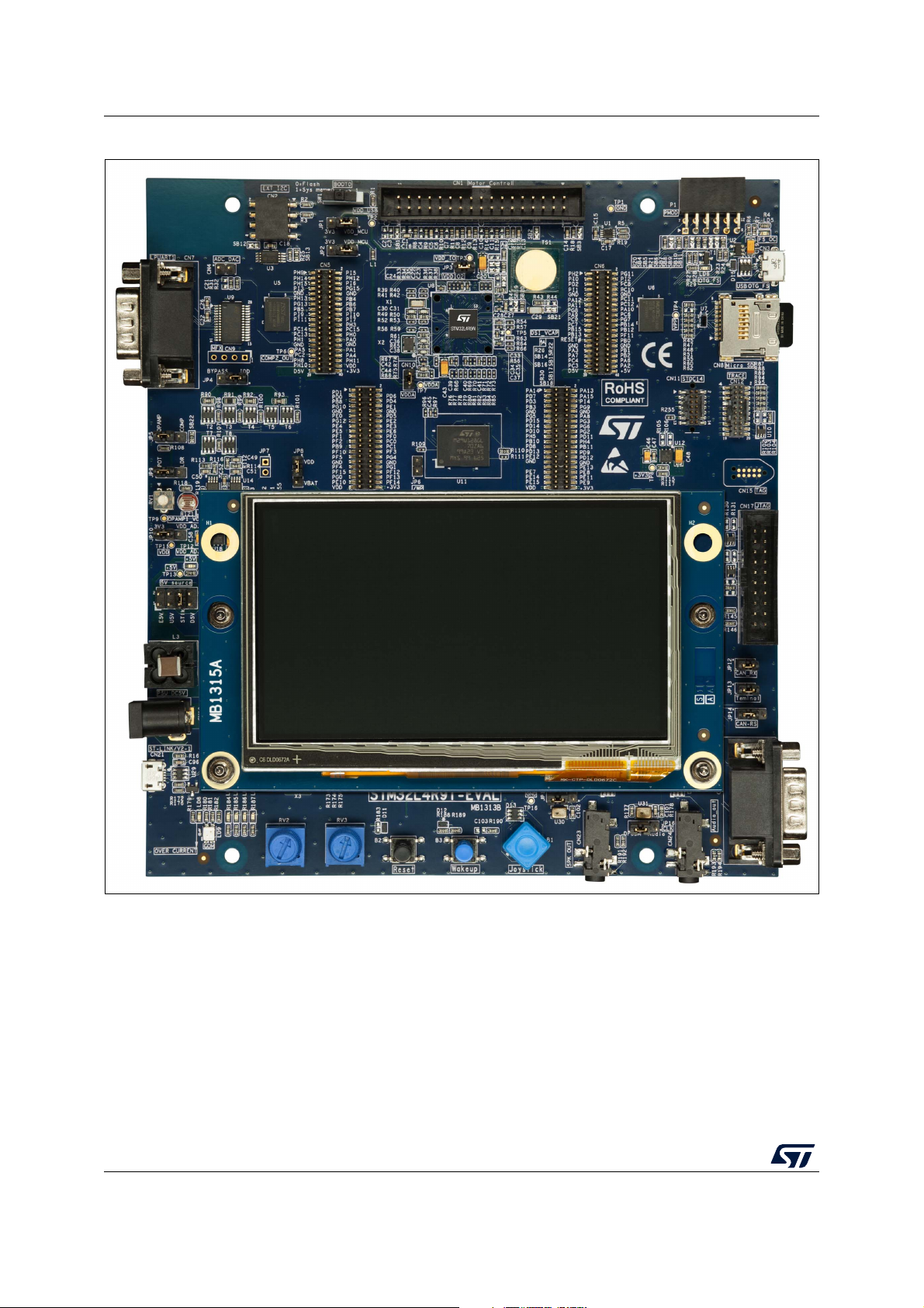
Figure 3. STM32L4R9I-EVAL board (top view) with round DSI display MB1314 daughterboard . . . 13
Figure 4. STM32L4R9I-EVAL board (top view) with TFT LCD MB1315 daughterboard . . . . . . . . . . 14
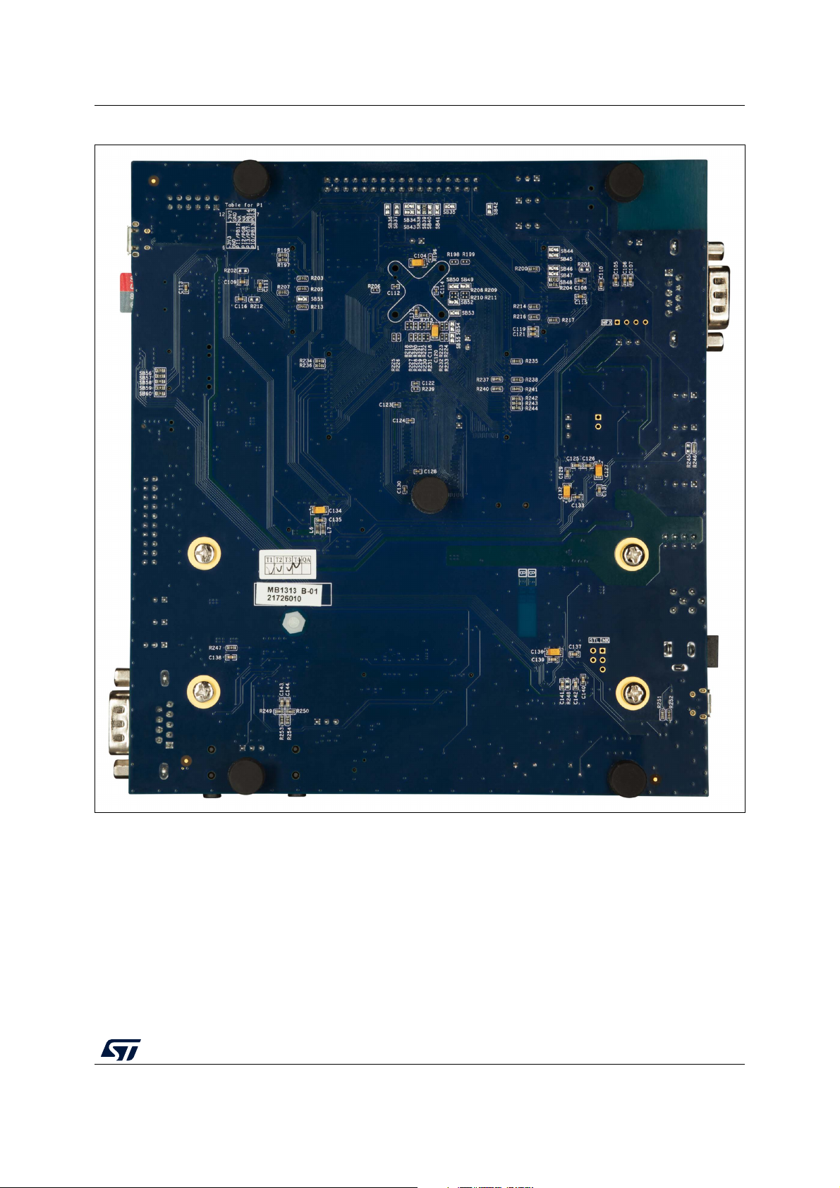
Figure 5. STM32L4R9I-EVAL board (bottom view) . . . . . . . . . . . . . . . . . . . . . . . . . . . . . . . . . . . . . . 15
Figure 6. MB1313 STM32L4R9I-EVAL board . . . . . . . . . . . . . . . . . . . . . . . . . . . . . . . . . . . . . . . . . . 16
Figure 7. MB1314 DSI display daughterboard . . . . . . . . . . . . . . . . . . . . . . . . . . . . . . . . . . . . . . . . . . 17
Figure 8. USB composite device . . . . . . . . . . . . . . . . . . . . . . . . . . . . . . . . . . . . . . . . . . . . . . . . . . . . 18
Figure 9. PCB top-side rework for motor control . . . . . . . . . . . . . . . . . . . . . . . . . . . . . . . . . . . . . . . . 31
Figure 10. PCB bottom-side rework for motor control . . . . . . . . . . . . . . . . . . . . . . . . . . . . . . . . . . . . . 32
Figure 11. CN1 motor-control connector (top view) . . . . . . . . . . . . . . . . . . . . . . . . . . . . . . . . . . . . . . . 49
Figure 12. CN2 EXT_I2C connector (front view) . . . . . . . . . . . . . . . . . . . . . . . . . . . . . . . . . . . . . . . . . 50
Figure 13. CN3 USB OTG FS Micro-AB connector (front view). . . . . . . . . . . . . . . . . . . . . . . . . . . . . . 50
Figure 14. CN4 analog input-output connector (top view) . . . . . . . . . . . . . . . . . . . . . . . . . . . . . . . . . . 51
Figure 15. RS232 D-sub male connector (front view) . . . . . . . . . . . . . . . . . . . . . . . . . . . . . . . . . . . . . 57
Figure 16. CN8 microSD™ connector (top view) . . . . . . . . . . . . . . . . . . . . . . . . . . . . . . . . . . . . . . . . . 57
Figure 17. CN11 STDC14 debugging connector (top view). . . . . . . . . . . . . . . . . . . . . . . . . . . . . . . . . 58
Figure 18. CN12 ETM trace debugging connector (top view) . . . . . . . . . . . . . . . . . . . . . . . . . . . . . . . 59
Figure 19. CN17 JTAG/SWD debugging connector (top view) . . . . . . . . . . . . . . . . . . . . . . . . . . . . . . 60
Figure 20. CN18 power-supply connector (front view) . . . . . . . . . . . . . . . . . . . . . . . . . . . . . . . . . . . . 61
Figure 21. CN21 USB Micro-B connector (front view) . . . . . . . . . . . . . . . . . . . . . . . . . . . . . . . . . . . . . 61
Figure 22. CN22 CAN D-type 9-pin male connector (front view) . . . . . . . . . . . . . . . . . . . . . . . . . . . . . 62
UM2248 Rev 4 7/72
7
Page 8

Features UM2248
1 Features
• STM32L4R9AII6 Arm
®(a)
-based microcontroller with 2 Mbytes of Flash memory and
640 Kbytes of RAM in a UFBGA169 package
• 1.2” 390x390 pixels MIPI DSI
SM
round LCD
• 4.3” 480x272 pixels TFT LCD with RGB mode
• Two ST-MEMS digital microphones
• 8-Gbyte microSD™ card bundled
• 16-Mbit (1 M x 16 bit) SRAM device
• 128-Mbit (8 M x 16 bit) NOR Flash memory device
• 512-Mbit Octo-SPI Flash memory device with double transfer rate (DTR) support
• 64-Mbit Octo-SPI SRAM memory device with HyperBus interface support
• EEPROM supporting 1 MHz I²C-bus communication speed
• Reset and wake-up/tamper buttons
• Joystick with four-way controller and selector
• Touch-sensing button
• Light-dependent resistor (LDR)
• Potentiometer
• Coin battery cell for power backup
• Board connectors:
– Two jack outputs for a stereo audio headphone with independent content
– Slot for microSD™ card supporting SD and SDHC
– TFT LCD standard connector
–MIPI DSI
SM
display standard connector
– EXT_I2C connector supports I²C bus
– RS-232 port configurable for communication or MCU flashing
– USB OTG FS Micro-AB port
– CAN 2.0A/B-compliant port
– Connector for ADC input and DAC output
– JTAG/SWD connector
– ETM trace debug connector
– User interface through USB virtual COM port
– Embedded ST-LINK/V2-1 debug and flashing facility
– TAG connector
– STDC14 connector
– PMOD connector
– Extension connector for the daughterboard
– Motor-control connector on the daughterboard
• Flexible power-supply options: power jack, ST-LINK/V2-1 USB connector,
a. Arm is a registered trademark of Arm Limited (or its subsidiaries) in the US and/or elsewhere.
8/72 UM2248 Rev 4
Page 9
UM2248 Ordering information
USB OTG FS connector, daughterboard
• On-board ST-LINK/V2-1 debugger/programmer with USB re-enumeration capability:
mass storage, virtual COM port and debug port
• Microcontroller supply voltage: fixed 3.3 V or adjustable range from 1.71 V to 3.6 V
• MCU current consumption measurement circuit
• Access to the comparator and operational amplifier of STM32L4R9AII6
• Comprehensive free software libraries and examples available with the STM32Cube
package
• Support of a wide choice of integrated development environments (IDEs) including IAR
Embedded Workbench
®
, MDK-ARM, and STM32CubeIDE
2 Ordering information
To order the STM32L4R9I-EVAL Evaluation board, refer to Ta bl e 1. Additional information is
available from the datasheet and reference manual of the target STM32.
Table 1. Ordering information
STM32L4R9I-EVAL
1. DSI display daughterboard
2. TFT LCD daughterboard
2.1 Codification
The meaning of the codification is explained in Tabl e 2.
STM32XXYY-EVAL Description Example: STM32L4R9I-EVAL
XX
YY
I
Order code
Board
reference
– MB1313
– MB1314
– MB1315
(1)
(2)
Targeted STM32
STM32L4R9AII6
Table 2. Codification explanation
MCU series in STM32 Arm
Cortex MCUs
STM32 product line
in the
series
STM32 Flash memory size:
– I for 2 Mbytes
STM32L4 Series
STM32L4R9
2 Mbytes
UM2248 Rev 4 9/72
71
Page 10

Development environment UM2248
3 Development environment
3.1 System requirements
• Windows® OS (7, 8, and 10), Linux® 64-bit, or macOS
• USB Type-A or USB Type-C® to Micro-B cable
3.2 Development toolchains
• IAR Systems - IAR Embedded Workbench
• Keil® - MDK-ARM
• STMicroelectronics - STM32CubeIDE
(b)
3.3 Demonstration software
The demonstration software, included in the STM32Cube MCU Package corresponding to
the on-board microcontroller, is preloaded in the STM32 Flash memory for easy
demonstration of the device peripherals in standalone mode. The latest versions of the
demonstration source code and associated documentation can be downloaded from
www.st.com.
®(b)
®(a)
4 Delivery recommendations
Before the first use, make sure that no damage occurred to the boards during shipment and
no socketed components are loosen in their sockets or fallen into the plastic bag.
In particular, pay attention to the following components:
1. microSD™ card in its CN8 receptacle
2. DSI display MB1314 daughterboard in its CN16 connector
For product information related to the STM32L4R9AII6 microcontroller, visit www.st.com
website.
5 Technology partners
MACRONIX: 512-Mbit Octo-SPI Flash, part number MX25LM51245GXDI00
a. macOS® is a trademark of Apple Inc. registered in the U.S. and other countries.
b. On Windows only
10/72 UM2248 Rev 4
Page 11
UM2248 Hardware layout and configuration
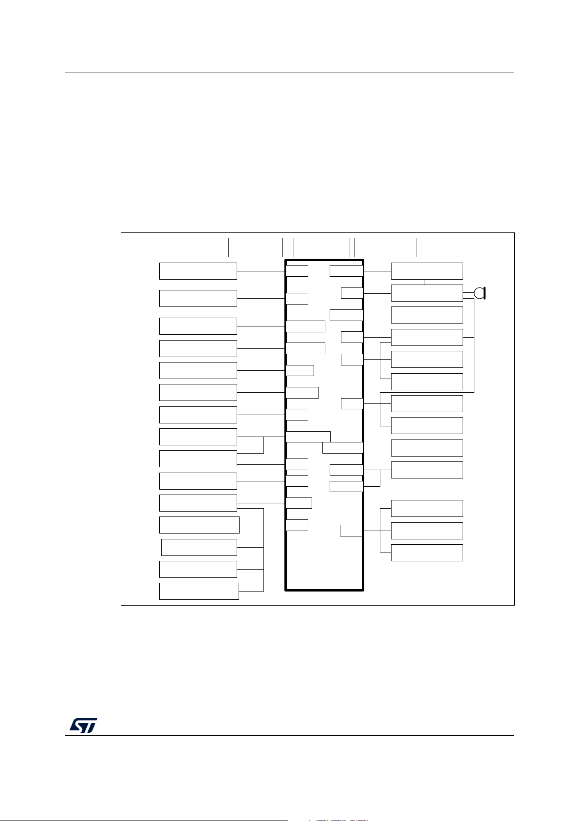
MSv46034V2
3.3 V
power supply
1.8 V
power supply
VDD ADJ
power supply
STM32L4R9AII6
UFBGA169
VBAT
RTC
Octo SPI1
Octo SPI2
SDIO1
OTG FS
TSC
LPUSART1
SPI2
CAN
UART3
DAP
DFSDM
SAI1
MIPI DSI
RGB
FMC
I2C2
ADC/DAC
OPAMP1
COMP2
GPIO
Audio codec
DSI LCD connector
TFT LCD connector
NOR Flash
SRAM/PSRAM
EEPROM
EXT_I2C connector
ADC/DAC connector
Potentiometer/LDR
Joystick/buttons
LEDs
Motor control
connector
PMOD connector
CAN connector
ST-LINK/V2-1
JTAG/SWD connector
TAG connector
Trace connector
STDC14 connector
3 V battery
32 KHz crystal
Octo SPI Flash
Octo SPI SRAM
microSD card
USB connector
One TS PAD
RS232 connector
MEMs
6 Hardware layout and configuration
The STM32L4R9I-EVAL board is designed around the STM32L4R9AII6 target
microcontroller in a UFBGA 169-pin package.
connections with peripheral components. Figure 2 shows the location of the main
components on the Evaluation board. Figure 3, Figure 4, and Figure 5 are the three images
showing the
STM32L4R9I-EVAL board top view with round DSI display, top view with TFT LCD, and
bottom view.
Figure 1. STM32L4R9I-EVAL hardware block diagram
Figure 1 illustrates the STM32L4R9AII6
UM2248 Rev 4 11/72
71
Page 12
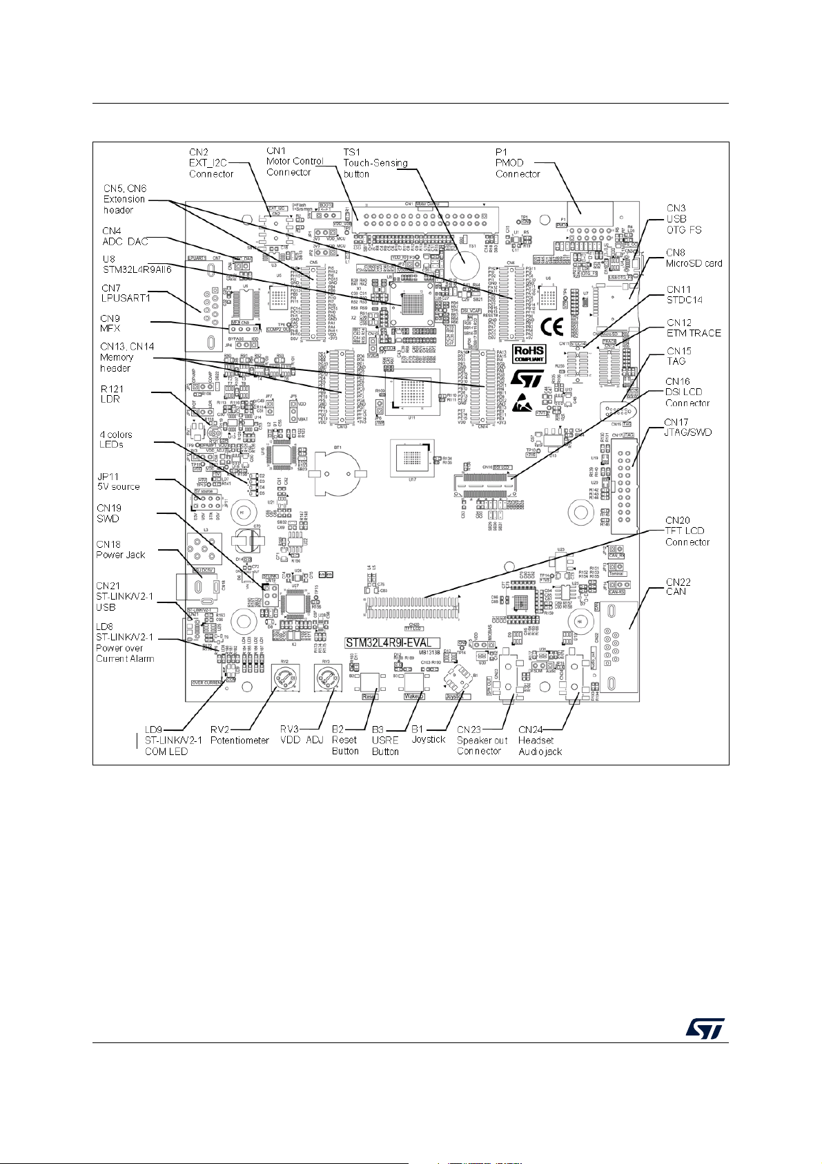
Hardware layout and configuration UM2248
Figure 2. STM32L4R9I-EVAL board (top side)
12/72 UM2248 Rev 4
Page 13
UM2248 Hardware layout and configuration
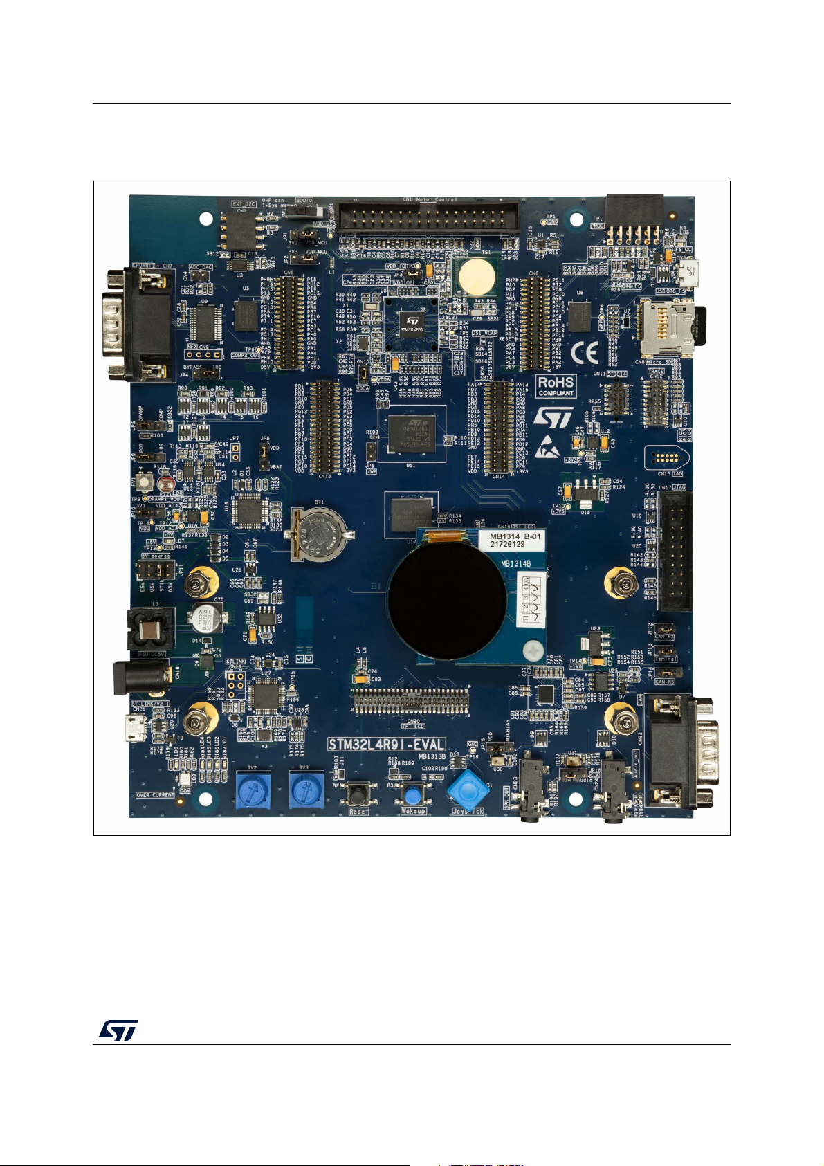
6.1 STM32L4R9I-EVAL board views
Figure 3. STM32L4R9I-EVAL board (top view) with round DSI display MB1314 daughterboard
Picture is not contractual
UM2248 Rev 4 13/72
71
Page 14
Hardware layout and configuration UM2248
Figure 4. STM32L4R9I-EVAL board (top view) with TFT LCD MB1315 daughterboard
Picture is not contractual
14/72 UM2248 Rev 4
Page 15
UM2248 Hardware layout and configuration
Figure 5. STM32L4R9I-EVAL board (bottom view)
Picture is not contractual
UM2248 Rev 4 15/72
71
Page 16
Hardware layout and configuration UM2248
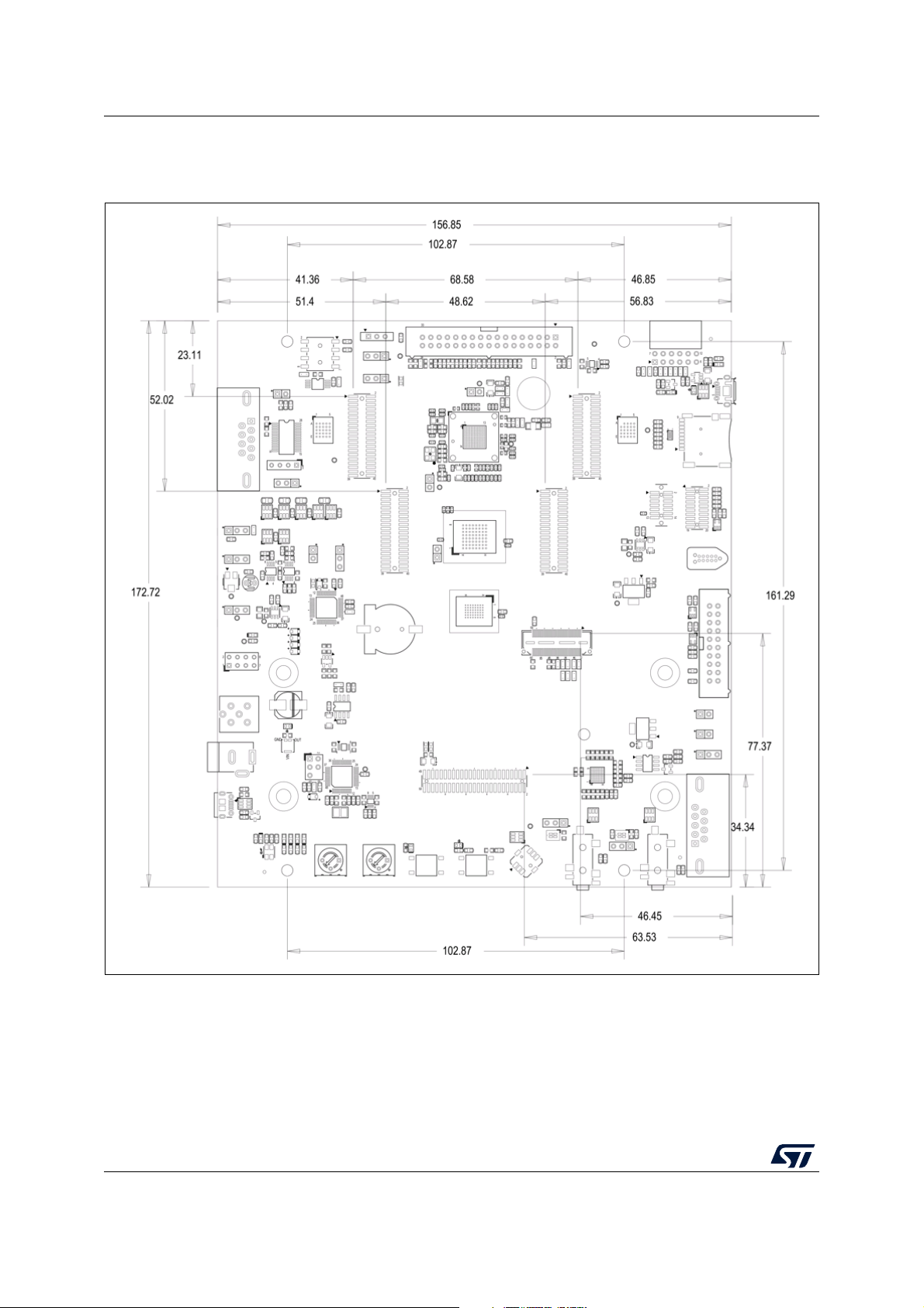
6.2 Mechanical dimensions
Figure 6. MB1313 STM32L4R9I-EVAL board
16/72 UM2248 Rev 4
Page 17
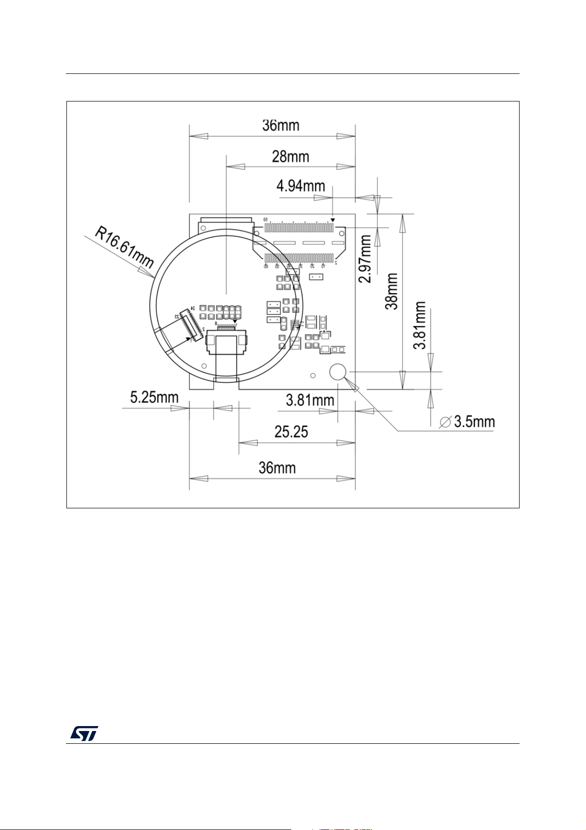
UM2248 Hardware layout and configuration
Figure 7. MB1314 DSI display daughterboard
6.3 ST-LINK/V2-1
ST-LINK/V2-1 facility for debugging and flashing of the STM32L4R9AII6 is integrated on the
STM32L4R9I-EVAL board.
Compared to the ST-LINK/V2 stand-alone tool available from STMicroelectronics, STLINK/V2-1 offers new features and drops some others.
New features:
• USB software re-enumeration
• Virtual COM port interface on USB
• Mass storage interface on USB
• USB power management request for more than 100mA power on USB
UM2248 Rev 4 17/72
71
Page 18
Hardware layout and configuration UM2248
Features dropped:
• SWIM interface
The CN21 USB connector can be used to power STM32L4R9I-EVAL regardless of the
ST-LINK/V2-1 facility use for debugging or for flashing STM32L4R9AII6. This holds also
when the ST-LINK/V2 stand-alone tool is connected to CN12, CN17, CN11, or CN15
connector and used for debugging or flashing STM32L4R9AII6. Section 6.5 provides more
details on powering STM32L4R9I-EVAL.
For full detail on both versions of the debug and flashing tool, the stand-alone ST-LINK/V2
and the embedded ST-LINK/V2-1, refer to www.st.com.
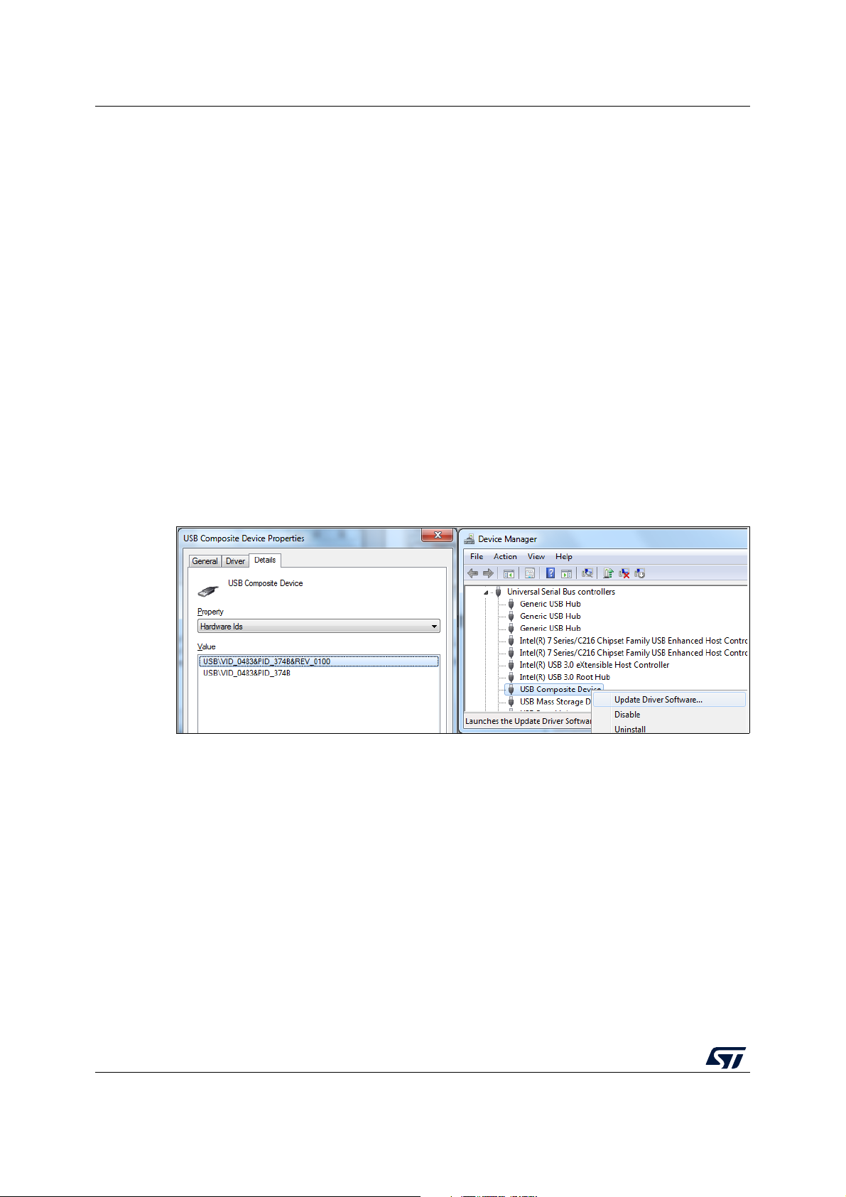
6.3.1 Drivers
Before connecting STM32L4R9I-EVAL to a Windows (XP, 7, 8 10) PC via USB, a driver for
ST-LINK/V2-1 must be installed. It is available from www.st.com.
In case the STM32L4R9I-EVAL board is connected to the PC before installing the driver, the
Windows device manager may report some USB devices found on STM32L4R9I-EVAL as
“Unknown”. To recover from this situation, after installing the dedicated driver downloaded
from www.st.com, the association of “Unknown” USB devices found on STM32L4R9I-EVAL
to this dedicated driver must be updated in the device manager manually. It is recommended
to proceed using the USB Composite Device line, as shown in
Figure 8.
Figure 8. USB composite device
6.3.2 ST-LINK/V2-1 firmware upgrade
For its operation, ST-LINK/V2-1 employs a dedicated MCU with Flash memory. Its firmware
determines ST-LINK/V2-1 functionality and performance. The firmware may evolve during
the life span of STM32L4R9I-EVAL to include new functionality, fix bugs, or support new
target microcontroller families. It is therefore recommended to keep ST-LINK/V2-1 firmware
up to date. The latest version is available from www.st.com.
6.4 ETM trace
The CN12 connector is available to output trace signals used for debugging. By default, the
Evaluation board is configured such that, STM32L4R9AII6 signals PE2, PE5, and PE6 are
not connected to trace outputs Trace_CK, Trace_D2, and Trace_D3 of CN12. They are
used for other functions.
18/72 UM2248 Rev 4
Page 19
UM2248 Hardware layout and configuration
Tabl e 3 shows the setting of configuration elements to shunt PE2, PE5, and PE6 MCU ports
to the CN12 connector, to use them as debug trace signals.
Table 3. Setting of configuration elements for CN12 trace connector
Element Setting Configuration
R53
SB56
R209
SB59
R211
SB60
SB56 open
SB56 closed
SB59 open
R209 out
SB59 closed
SB60 open
R211 out
SB60 closed
Warning: Enabling the CN12 trace outputs through hardware modifications described in
Tabl e 3 results in reducing the memory address bus width to 20 address lines and so the
addressable space to 1 Mword of 16 bits. As a consequence, the onboard SRAM and NOR
Flash memory usable capacity is reduced to 16 Mbits.
6.5 Power Supply
The STM32L4R9I-EVAL board is designed to be powered from 5 V DC power source. It
incorporates a precise polymer Zener diode (Poly-Zen) protecting the board from damage
due to the wrong power supply. One of the following four 5
an appropriate board configuration:
• Power jack CN18 marked PSU_DC5V on the board. A jumper must be placed in E5V
location of JP11. The positive pole is on the center pin as illustrated in Figure 20.
• Micro-B USB receptacle CN21 of ST-LINK/V2-1 provides up to 500mA to the board.
Offering enumeration feature described in Section 6.5.1.
• Micro-AB USB receptacle CN3 of USB OTG interface marked USB OTG_FS on the
board, supplies up to 500mA to the board.
• Pin 39 of CN5 and Pin 39 of CN6 extension connectors for a custom daughterboard,
marked D5V on the board.
R53 in
R53 out
R209 in
R211 in
Default setting.
PE2 connected to memory address line A23.
PE2 connected to Trace_CK on CN12. A23 pulled down.
Default setting.
PE5 connected to memory address line A21.
PE5 connected to Trace_D2 on CN12. A21 pulled down.
Default setting.
PE6 connected to memory address line A22.
PE6 connected to Trace_D3 on CN12. A22 pulled down.
V DC power inputs is usable with
No external power supply is provided with the board.
LD7 red LED turns on when the voltage on the power line marked as +5 V is present. All
supply lines required for the operation of the components on STM32L4R9I-EVAL are
derived from that +5
V line.
Table 4 describes the setting of all jumpers related to powering the STM32L4R9I-EVAL and
its extension board. VDD_MCU is STM32L4R9AII6 digital supply voltage line. It is possible to
drive the boards with either fixed 3.3
RV3 potentiometer and producing a range of voltages between 1.71
V or with an adjustable voltage regulator controlled by
V and 3.6 V.
UM2248 Rev 4 19/72
71
Page 20

Hardware layout and configuration UM2248
6.5.1 Supplying the board through ST-LINK/V2-1 USB port
To power STM32L4R9I-EVAL in this way, the USB host (a PC) gets connected with the
STM32L4R9I-EVAL board’s Micro-B USB receptacle, via a USB cable. This event is the
beginning of the USB enumeration procedure. In its initial phase, the host’s USB port
current supply capability is limited to 100 mA. It is enough because only the ST-LINK/V2-1
part of STM32L4R9I-EVAL draws power at that time. If the SB33 solder bridge is open, the
U22 ST890 power switch is set in the OFF position, which isolates the remainder of
STM32L4R9I-EVAL from the power source. In the next phase of the enumeration
procedure, the host PC informs the ST-LINK/V2-1 facility of its capability to supply up to 300
mA of current. If the answer is positive, the ST-LINK/V2-1 sets the U22 ST890 switch to ON
position to supply power to the remainder of the STM32L4R9I-EVAL board. If the PC USB
port is not capable of supplying up to 300 mA of current, the CN18 power jack is available to
supply the board.
If a short-circuit occurs on the board, the ST890 power switch protects the USB port of the
host PC against a current exceeding 600 mA. In such an event, the LD8 LED lights on.
The STM32L4R9I-EVAL board is also supply-able from a USB power source not supporting
enumeration, such as a USB charger, as shown in
power switch ON regardless of the enumeration procedure result and passes the power
unconditionally to the board.
The LD7 red LED turns on whenever the whole board is powered.
Table 4. ST-LINK/V2-1 turns the ST890
6.5.2 Using ST-LINK/2-1 along with powering through the CN18 power jack
If the board requires more than 300 mA of supply current, this cannot be provided by the
host PC connected to the ST-LINK/2-1 USB port, used for debugging or flashing
STM32L4R9AII6. In such a case, the board is supplied through CN18 (marked PSU_DC5V
on the board).
To do this, it is important to power the board before connecting it with the host PC, which
requires the following sequence to be respected:
1. Set the jumper in JP11 header in E5V position,
2. Connect the external 5 V power source to CN18,
3. Check the red LED LD7 is turned on,
4. Connect the host PC to the CN12 USB connector.
In case the board requires more than 300 mA and the host PC is connected via USB before
the board is powered from CN18, there is a risk of the following events to occur, in the order
of severity:
1. The host PC is capable of supplying 300 mA (the enumeration succeeds) but it does
not incorporate any over-current protection on its USB port. It is damaged due to overcurrent.
2. The host PC is capable of supplying 300 mA (the enumeration succeeds) and it has
built-in over-current protection on its USB port, limiting or shutting down the power out
of its USB port when the excessive current requirement from STM32L4R9I-EVAL is
detected. This causes an operating failure to STM32L4R9I-EVAL.
3. The host PC is not capable of supplying 300 mA (the enumeration fails) so ST-LINK/V21 does not supply the remainder of STM32L4R9I-EVAL from its USB port V
BUS
line.
20/72 UM2248 Rev 4
Page 21
UM2248 Hardware layout and configuration
E5V
U5V
STlk D5V
E5V
U5V
STlk D5V
E5V
U5V
STlk D5V
E5V
U5V
STlk D5V
E5V
U5V
STlk D5V
1
3
2
1
3
2
1
3
2
1
3
2
1
3
2
1
3
2
Jumper /
solder
bridge
JP11
Power
source
selector
JP8
Vbat
connection
JP10
VDD_MCU
connection
JP1
VDD_USB
connection
Table 4. Power supply related jumpers settings
Setting Configuration
STM32L4R9I-EVAL is supplied through the CN18 power
jack (marked PSU_DC5V). CN5 and CN6 extension
connectors do not pass the 5 V of STM32L4R9I-EVAL to the
daughterboard.
STM32L4R9I-EVAL is supplied through the CN3 Micro-AB
USB connector. CN5 and CN6 extension connectors do not
pass the 5 V of STM32L4R9I-EVAL to the daughterboard.
Default setting.
STM32L4R9I-EVAL is supplied through the CN21 Micro-B
USB connector. CN5 and CN6 extension connectors do not
pass the 5 V of STM32L4R9I-EVAL to the daughterboard.
STM32L4R9I-EVAL is supplied through pin 39 of CN5 and
pin 39 of CN6 extension connectors.
STM32L4R9I-EVAL is supplied through the CN18 power
jack. CN5 and CN6 extension connectors pass the 5 V of
STM32L4R9I-EVAL to the daughterboard. Make sure to
disconnect from the daughterboard, any power supply that
may generate conflict with the power supply on the CN18
power jack.
Vbat is connected to the battery.
Default setting.
Vbat is connected to VDD.
Default setting.
VDD_MCU (VDD terminals of STM32L4R9AII6) is
connected to fixed +3.3 V.
VDD_MCU is connected to voltage in the range from
+1.71 V to +3.6 V, adjustable with potentiometer RV3.
Default setting.
VDD_USB (VDD USB terminal of STM32L4R9AII6) is
connected with VDD_MCU.
VDD_USB is connected to +3.3 V.
UM2248 Rev 4 21/72
71
Page 22
Hardware layout and configuration UM2248
1
3
2
1
3
2
1
2
1
2
Table 4. Power supply related jumpers settings (continued)
Jumper /
solder
bridge
JP2
VDDA
connection
Setting Configuration
Default setting.
VDDA terminal of STM32L4R9AII6 is connected with
VDD_MCU.
VDDA terminal of STM32L4R9AII6 is connected to +3.3 V.
JP3
VDD_IO
connection
SB33
SB33 Off
Powering
through
USB of
ST-LINK/
V2-1
1. On all ST-LINK/V2-1 boards, the target application is now able to run even if the ST-LINK/V2-1 is either not
connected to a USB host, or is powered through a USB charger (or through a not-enumerating USB host).
SB33 On
6.6 Clock references
Two clock references are available on STM32L4R9I-EVAL for the STM32L4R9AII6
microcontroller.
• 32.768 kHz crystal X1, for embedded RTC
• 25 MHz crystal X2, for the main clock generator
Default setting.
VDD_IO (VDDIO2 terminals of STM32L4R9AII6) is
connected with VDD_MCU.
VDD_IO is open.
Default setting.
The CN21 ST-LINK/V2-1 Micro-B USB connector can be
used to supply power to the STM32L4R9I-EVAL board
remainder, depending on the powering capability of the host
PC USB port declared in the enumeration.
CN21 Micro-B USB connector of ST-LINK/V2-1 supplies
power to the STM32L4R9I-EVAL board remainder. This is
the setting for powering the board through CN21 using a
USB charger)
(1)
.
The main clock generation is possible via an internal RC oscillator, disconnected by removing
resistors R61 and R65 when the internal RC clock is used.
Solder
bridge
SB50
22/72 UM2248 Rev 4
Table 5. X1 crystal related solder bridge settings
Setting Configuration
Default setting.
Open
Closed
PC14 OSC32_IN terminal is not routed to the CN5 extension
connector. X1 is used as the clock reference.
PC14 OSC32_IN is routed to the CN5 extension connector.
Resistor R50 must be removed, for the X1 quartz circuit not to
disturb the clock reference or source on the daughterboard.
Page 23

UM2248 Hardware layout and configuration
Table 5. X1 crystal related solder bridge settings (continued)
Solder
bridge
SB49
Solder
bridge
SB52
SB53
Setting Configuration
Default setting.
Open
Closed
PC15 OSC32_OUT terminal is not routed to the CN5 extension
connector. X1 is used as the clock reference.
PC15 OSC32_OUT is routed to the CN5 extension connector.
Resistor R49 must be removed, for the X1 quartz circuit not to
disturb clock reference on the daughterboard.
Table 6. X2 crystal related solder bridge settings
Setting Configuration
Default setting.
Open
Closed
Open
Closed
PH0 OSC_IN terminal is not routed to the CN5 extension
connector. X2 is used as the clock reference.
PH0 OSC_IN is routed to the CN5 extension connector. Resistor
R61 must be removed, in order not to disturb clock reference or
source on the daughterboard.
Default setting.
PH1 OSC_OUT terminal is not routed to the CN5 extension
connector. X2 is used as the clock reference.
PH1 OSC_OUT is routed to the CN5 extension connector. Resistor
R65 must be removed, in order not to disturb clock reference or
source on the daughterboard.
6.7 Reset sources
The reset signal of the STM32L4R9I-EVAL board is active LOW.
Sources of reset are listed below:
• reset button B2
• CN17 JTAG/SWD connector, CN12 ETM trace connector, CN11 STDC14 connector
and CN15 TAG connector (reset from debug tools)
• reset through pin 27 of CN6 extension connector (reset from daughterboard)
• embedded ST-LINK/V2-1
6.8 Boot option
After reset, the STM32L4R9AII6 MCU boot is available from the following embedded
memory locations:
• main (user, non-protected) Flash memory
• system (protected) Flash memory
• RAM, for debugging
UM2248 Rev 4 23/72
71
Page 24

Hardware layout and configuration UM2248
0<->1
0<->1
The boot option is configured by setting switch SW1 (BOOT) and the boot base address
programmed in the nBOOT1, nBOOT0, and nSWBOOT0 of FLASH_OPTR option bytes.
Switch Setting Description
SW1
Table 7. Boot selection switch
Default setting.
BOOT0 line is tied low. STM32L4R9AII6 boots from main Flash
memory or system memory.
BOOT0 line is tied high. STM32L4R9AII6 boots from system Flash
memory (nBOOT1 bit of FLASH_OPTR register is set high) or from
RAM (nBOOT1 is set low).
6.8.1 Bootloader limitations
Boot from system Flash memory results in executing bootloader code stored in the system
Flash memory protected against writing and erasing. This allows in-system programming
(ISP), that is, flashing the STM32 user Flash memory. It also allows writing data into RAM.
The data come in via one of the communication interfaces such as USART, SPI, I2C bus,
USB, or CAN.
The bootloader version is identified by reading the Bootloader ID at the address
0x1FFF6FFE: the content is 0x91 for bootloader V9.1 and 0x92 for V9.2.
The STM32L4R9AII6 part soldered on the STM32L4R9I-EVAL main board is marked with a
date code corresponding to its date of manufacturing. STM32L4R9AII6 parts with a date
code prior or equal to week 37 of 2017 are fitted with bootloader V9.1 affected by the
limitations to be worked around, as described hereunder. Parts with the date code starting
from week 38 of 2017 contain bootloader V9.2 in which the limitations no longer exist.
To locate the visual date code information on the STM32L4R9II6 package, refer to its
datasheet (DS12023) available at www.st.com, section Package Information. Date code
related portion of the package marking takes Y WW format, where Y is the last digit of the
year and WW is the week. For example, a part manufactured in week 38 of 2017 bares the
date code 7 38.
There is also another way to identify the need for a workaround: before opening the blister
of the Discovery Kit, just check the backside of the blister. At the bottom left side, if the
reference number is equal or higher than 32L4R9IDISCO/ 02-0, it means the bootloader
version is V9.2 and there is no need to apply a workaround. Any other inferior number like
01-0 needs the workaround.
The bootloader ID for the bootloader V9.1 is 0x91.
The following limitation exists in the bootloader V9.1:
Some user Flash memory data get corrupted when written via SPI interface
Description:
During bootloader SPI Write Flash operation, some random 64-bits (2 double-words) may
be left blank at 0xFF.
Workarounds:
24/72 UM2248 Rev 4
Page 25

UM2248 Hardware layout and configuration
1
3
2
1
3
2
1
3
2
1
3
2
WA1: add a delay between sending the Write command and its ACK request. Its duration
must be the duration of the 256-Byte Flash write time.
WA2: read back after each writing operation (256 bytes or at end of user code flashing) and
in case of error start writing again.
WA3: Using bootloader, load a patch code in RAM to write in Flash memory through the
same Write Memory write protocol as bootloader (code provided by ST).
6.9 Audio
A codec connected to the STM32L4R9AII6 SAI interface supports the DSAI port TDM
feature. This offers STM32L4R9AII6 the capability to simultaneously stream two
independent stereo audio channels to two separate stereo analog audio outputs.
There are two digital microphones on the STM32L4R9I-EVAL board.
6.9.1 Digital microphones
U30 and U31 on the STM32L4R9I-EVAL board are MP34DT01TR MEMS digital
omnidirectional microphones providing PDM (pulse density modulation) outputs. To share
the same data line, their outputs are interlaced. The combined data output of the
microphones is directly routed to STM32L4R9AII6 terminals, thanks to the integrated input
digital filters. The microphones are supplied with a programmable clock generated directly
by STM32L4R9AII6.
As an option, the microphones are connected to U26 WM8994, the Wolfson audio codec
device. In that configuration, U26 also supplies the PDM clock to the microphones.
Regardless of where the microphones are routed to, STM32L4R9AII6 or WM8994, their
power supplier is either VDD or MICBIAS1 output of the WM8994 codec device.
Tabl e 8 shows the settings of all jumpers associated with the digital microphones on the
board.
Jumper Setting Configuration
JP16
JP15
Table 8. Digital microphone-related jumper settings
The PDM clock for digital microphones comes from the WM8994
codec.
Default setting.
The PDM clock for digital microphones comes from
STM32L4R9AII6.
The power supply of digital microphones is generated by
WM8994 codec.
Default setting.
The power supply of digital microphones is V
DD
.
UM2248 Rev 4 25/72
71
Page 26

Hardware layout and configuration UM2248
6.9.2 Headphones outputs
The STM32L4R9I-EVAL board potentially drives two sets of stereo headphones. Identical or
different stereo audio contents are played back in each set of headphones. STM32L4R9AII6
sends up to two independent stereo audio channels, via its SAI1 TDM port, to the WM8994
codec device. The codec device converts the digital audio stream to stereo analog signals. It
then boosts them for direct drive of headphones connecting to 3.5
on the board, CN24 for Audio-output1, and CN23 for Audio_output2.
The CN23 jack takes its signal from the output of the WM8994 codec device intended for
driving an amplifier for loudspeakers. A hardware adaptation is incorporated on the board to
make it compatible with a direct headphone drive. The adaptation consists of coupling
capacitors blocking the DC component of the signal, attenuator, and anti-pop resistors. The
loudspeaker output of the WM8994 codec device must be configured by software in a linear
mode called “class AB” and not in a switching mode called “class D”.
The I²C-bus address of WM8994 is 0b0011 010x.
mm stereo jack receptacles
6.9.3 Limitations in using audio features
Due to the share of some terminals of STM32L4R9AII6 by multiple peripherals, the following
limitations apply in using the audio features:
• If the SAI1_MCLKA and SAI1_FSA are used as part of SAI1 port, it cannot be used as
CAN peripheral.
• If the SAI1_SDB is used as part of the SAI1 port, it cannot be used as the Comp2_OUT
signal.
• If the SAI1 port of STM32L4R9AII6 is used for streaming audio to the WM8994 codec
IC, STM32L4R9AII6 cannot control the motor.
• If the digital microphones are attached to STM32L4R9AII6, control the motor cannot be
driven.
6.10 USB OTG FS port
The STM32L4R9I-EVAL board supports USB OTG full-speed (FS) communication. The
CN3 USB OTG connector is Micro-AB type.
6.10.1 STM32L4R9I-EVAL used as a USB device
When a “USB host” connection to the CN3 Micro-AB USB connector of STM32L4R9I-EVAL
is detected, the board starts behaving like a “USB device”. Depending on the powering
capability of the USB host, the board potentially takes power from the V
In the board schematic diagrams, the corresponding power voltage line is called U5V.
Section 6.5 provides information on how to set associated jumpers for this powering option.
The resistor R23 must be left open to prevent STM32L4R9I-EVAL from sourcing 5 V to the
V
terminal, which would cause conflict with the 5 V sourced by the USB host. This may
BUS
happen if the MFX_GPIO6 is controlled by the software of the MFX MCU such that, it enables
the output of the U2 power switch.
26/72 UM2248 Rev 4
terminal of CN3.
BUS
Page 27

UM2248 Hardware layout and configuration
6.10.2 STM32L4R9I-EVAL used as a USB host
When a “USB device” connection to the CN3 Micro-AB USB connector is detected, the
STM32L4R9I-EVAL board starts behaving like a “USB host”. It sources 5
terminal of the CN3 Micro-AB USB connector to power the USB device. For this to happen,
the STM32L4R9AII6 sets the U2 power switch STMPS2151STR to ON state. The LD6
green LED marked OTG_FS indicates that the peripheral is supplied from the board. The
LD5 red LED marked FS_OC lights up if over-current is detected. The resistor R23 must be
closed to allow the MFX_GPIO6 from MFX MCU to control the U2 power switch.
In any other STM32L4R9I-EVALpowering option, the resistor R23 must be open, to avoid
accidental damage caused to an external USB host.
V on the V
BUS
6.10.3 Limitations in using USB OTG FS port
The USB OTG FS port operation is exclusive with motor control
6.10.4 Operating voltage
The USB-related operating supply voltage of STM32L4R9AII6 (VDD_USB line) must be within
the range from 3.0
V to 3.6 V.
6.11 RS232 port
The STM32L4R9I-EVAL board offers one RS-232 communication port. The RS-232
communication port uses the CN7 DB9 male connector. RX, TX, RTS, and CTS signals of
the STM32L4R9AII6 LPUSART1 interface are routed to CN7.
6.11.1 Operating voltage
The RS-232 operating supply voltage of STM32L4R9AII6 (VDD line) must be within the range
from 1.71
V to 3.6 V.
6.12 microSD™ card
The CN8 slot for microSD™ card is routed to STM32L4R9AII6 SDIO port, accepting SD (up to
2
Gbytes) and SDHC (up to 32 Gbytes) cards. One 8-Gbyte microSD™ card is delivered as
part of STM32L4R9I-EVAL. The card insertion switch is routed to the MFX_GPIO5 of MFX
MCU port.
6.12.1 Limitations
Due to the share of SDIO port, the following limitations apply:
• The microSD™ card cannot be operated simultaneously with motor control.
• The microSD™ card cannot be operated for 4 bits date when SDIO_D1 and SDIO_D2
used as Trace_D0 and Trace_D1 signals.
6.12.2 Operating voltage
The supply voltage for the STM32L4R9I-EVAL microSD™ card operation must be within the
range from 2.7
V to 3.6 V.
UM2248 Rev 4 27/72
71
Page 28

Hardware layout and configuration UM2248
6.13 Motor control
The CN1 connector is designed to receive a motor-control (MC) module. Table 9 shows the
assignment of CN1 and STM32L4R9AII6 terminals.
Table 9 also lists the modifications to be made on the board versus its by-default
configuration. Refer to Section 6.13.1 for further details.
Table 9. Motor-control terminal and function assignment
CN1 motor-control
connector
Ter min al
1
2GND- GND --
3 PWM_1H PC6 TIM8_CH1 -
4GND- GND --
5 PWM_1L PH13 TIM8_CH1N -
6GND- GND --
7 PWM_2H PC7 TIM8_CH2 -
8GND- GND --
9 PWM_2L PH14 TIM8_CH2N -
10 GND - GND - -
Terminal
name
Emergency
Stop
Port
name
PI4 TIM8_BKIN -
STM32L4R9AII6 microcontroller
Function
Alternate
function
Close SB3.
Remove R234.
Close SB21.
Remove R44 or no
daughterboard.
Close SB46.
Remove R186.
Close SB19.
Open SB20.
Remove R46 or no
daughterboard.
Close SB44.
Remove R185.
Board modifications for
enabling motor control
11 PWM_3H PC8 TIM8_CH3 -
12 GND - GND - -
13 PWM_3L PH15 TIM8_CH3N -
14 Bus Voltage PC4 ADC1_IN13 -
15
16
28/72 UM2248 Rev 4
PhaseA
current+
PhaseA
current-
PC0 ADC1_IN1 -
-GND --
Close SB2.
Remove R195.
Close SB45.
Remove R184.
Close SB55.
Remove R75.
Close SB36.
Remove R242.
Page 29

UM2248 Hardware layout and configuration
Table 9. Motor-control terminal and function assignment (continued)
CN1 motor-control
connector
Ter min al
17
18
19
20
Terminal
name
PhaseB
current+
PhaseB
current-
PhaseC
current+
PhaseC
current-
Port
name
PC1 ADC1_IN2 -
-GND --
PC2 ADC1_IN3 -
-GND --
STM32L4R9AII6 microcontroller
Function
Alternate
function
21 ICL Shutout PG9 GPIO -
22 GND - GND - -
23
24
Dissipative
Brake
PFC indirect
current
PG13 GPIO -
PA0 ADC1_IN5 -
25 +5V - +5V - -
Board modifications for
enabling motor control
Close SB37.
Remove R244.
Close SB43.
Remove R217.
Close SB34.
Remove R236.
Close SB47.
Remove SB29 and no board
on the PMOD connector.
Close SB38
Remove R214 and SB39
26
Heatsink
Te mp .
PA1 ADC1_IN6 -
27 PFC Sync PB14 TIM15_CH1 -
28 +3.3V - +3.3V - -
29 PFC PWM PB15 TIM15_CH2 -
30
PFC
Shutdown
PA9 TIM15_BKIN -
31 Encoder A PB6 TIM4_CH1 ADC12_IN
32 PFC Vac PC3 ADC1_IN4 -
Close SB40.
Remove R216.
Close SB41.
Remove R207 and no board
on the PMOD connector.
Close SB51.
Remove R187.
Close SB35.
Remove R203.
Close SB14.
Remove SB15 and SB16.
Remove R26 or no
daughterboard.
Close SB54.
Remove R67.
UM2248 Rev 4 29/72
71
Page 30

Hardware layout and configuration UM2248
Table 9. Motor-control terminal and function assignment (continued)
CN1 motor-control
connector
Ter min al
33 Encoder B PB7 TIM4_CH2 ADC12_IN
34
Terminal
name
Encoder
Index
Port
name
PB8 TIM4_CH3 ADC12_IN
STM32L4R9AII6 microcontroller
Function
Alternate
function
6.13.1 Board modifications to enable motor control
Figure 9 (top side) and Figure 10 (bottom side) illustrate the board modifications listed in
Table 9, required for the operation of motor control. The red color denotes a component to be
removed. The green color denotes a component to be fitted.
6.13.2 Limitations
Motor-control operation is exclusive with Octo-SPIP1 Flash memory device, audio codec,
potentiometer, LDR, microSD™ card, LED1 to LED4 drive, MEMS, MFX, PMOD, USB
OTG_FS, TFT LCD connector, DSI display connector, and touch sensing.
Board modifications for
enabling motor control
Close SB17.
Remove SB18.
Remove R30 or no
daughterboard.
Close SB42.
Remove R235 and open JP12.
30/72 UM2248 Rev 4
Page 31

UM2248 Hardware layout and configuration
Figure 9. PCB top-side rework for motor control
UM2248 Rev 4 31/72
71
Page 32

Hardware layout and configuration UM2248
Figure 10. PCB bottom-side rework for motor control
32/72 UM2248 Rev 4
Page 33

UM2248 Hardware layout and configuration
1
3
2
1
3
2
1
2
1
2
1
2
1
2
6.14 CAN
The STM32L4R9I-EVAL board supports one CAN2.0A/B channel compliant with CAN
specification. The CN22 DB9 male connector is available as the CAN interface.
A 3.3 V CAN transceiver is fitted between the CN22 connector and the CAN controller port
of STM32L4R9AII6.
The JP14 jumper selects one of the high-speed, standby, and slope control modes of the CAN
transceiver. The JP13 jumper allows integrating a CAN termination resistor. The JP12 is used
to connected the CAN transceiver avoiding unknown signals from the CAN transceiver.
Jumper Setting Configuration
JP14
Table 10. CAN related jumpers
Default setting.
CAN transceiver operates in high-speed mode.
CAN transceiver is in standby mode.
JP13
JP12
6.14.1 Limitations
CAN operation is exclusive with the audio codec and MC operation.
6.14.2 Operating voltage
The supply voltage for STM32L4R9I-EVAL CAN operation must be within the range from
3.0
V to 3.6 V.
Default setting.
Termination resistor fitted on CAN physical link.
No termination resistor on CAN physical link.
Default setting.
CAN_TX is not used for CAN transceiver.
CAN_TX is used from the STM32L4R9AII6 terminal.
UM2248 Rev 4 33/72
71
Page 34

Hardware layout and configuration UM2248
6.15 Extension connectors CN5, CN6, CN13, and CN14
The CN5, CN6, CN13, and CN14 headers complement to give access to all GPIOs of the
STM32L4R9AII6 microcontroller. In addition to GPIOs, the following signals and power
supply lines are also routed on CN5 or CN6 or CN13 or CN14:
• GND
• +5 V
• +3.3 V
• D5V
• VDD
• RESET#
• Clock terminals PC14-OSC32_IN, PC15-OSC32_OUT, PH0-OSC_IN, PH1-OSC_OUT
Each header has two rows of 20 pins, with 1.27 mm pitch and 2.54 mm row spacing. For
extension modules, SAMTEC RSM-120-02-L-D-xxx and SMS-120-x-x-D are recommendable
as SMD and through-hole receptacles, respectively (x is a wild card).
6.16 User LEDs
Four general-purpose color LEDs (LD1, LD2, LD3, LD4) are available as light indicators.
Each LED is ON with a low level of the corresponding ports of STM32L4R9AII6.
And the four LEDs are exclusive with MC operation.
6.17 Physical input devices
The STM32L4R9I-EVAL board provides several input devices for physical human control,
listed below:
• four-way joystick controller with select key (B1)
• wake-up/ tamper button (B3)
• reset button (B2)
• 10 kΩ potentiometer (RV2)
• light-dependent resistor, LDR (R121)
The potentiometer and the light-dependent resistor are mutually exclusively rout-able to either
PB4 or PA0 port of STM32L4R9AII6.
jumpers.
As illustrated in the schematic diagram, the PB4 port is routed, in the STM32L4R9AII6, to the
non-inverting input of comparator Comp2. The PA0 is routed to the non-inverting input of the
operational amplifier OpAmp1.
Tabl e 11 depicts the setting of associated configuration
34/72 UM2248 Rev 4
Page 35

UM2248 Hardware layout and configuration
1
3
2
1
3
2
1
3
2
1
3
2
1
3
2
1
3
2
1
3
2
1
3
2
Table 11. Port assignment for control of physical input devices
Jumper Setting Routing
JP9
A potentiometer is routed to pin PB4 o fSTM32L4R9AII6.
JP5
JP9
Default setting.
A potentiometer is routed to pin PA0 of STM32L4R9AII6.
JP5
JP9
LDR is routed to pin PB4 of STM32L4R9AII6.
JP5
JP9
LDR is routed to pin PA0 of STM32L4R9AII6.
JP5
6.17.1 Limitations
The potentiometer and the light-dependent resistor are exclusive with MFX, audio codec,
OctoSPIP1, the debugging connector, and MC operation. They are mutually exclusive.
6.18 Operational amplifier and comparator
6.18.1 Operational amplifier
STM32L4R9AII6 provides two onboard operational amplifiers, one of which, OpAmp1, is
made accessible on STM32L4R9I-EVAL. OpAmp1 has its inputs and its output routed to I/O
ports PA0, PA1, and PA3, respectively. The non-inverting input PA0 is accessible on the
terminal 1 of the JP5 jumper header. On top of the possibility of routing either of the
potentiometer or LDR to PA0, an external source is also connectible to it, using the terminal
1 of JP5.
The PA3 output of the operational amplifier is accessible on test point TP9. Refer to the
schematic diagram.
The gain of OpAmp1 is determined by the ratio of the variable resistor RV1 and the resistor
R246, as shown in the following equation:
Gain = 1 + RV1 / R246
With the RV1 ranging from 0 to 10 kΩ and R246 being 1 kΩ, the gain varies from 1 to 11.
UM2248 Rev 4 35/72
71
Page 36

Hardware layout and configuration UM2248
The R108 resistor in series with PA0 is beneficial for reducing the output offset.
Table 12 shows the configuration elements and their settings allowing them to access the
OpAmp1 function.
Element Setting Configuration
SB39
SB38
R214
Table 12. Configuration elements related to OpAmp1
SB38 open
SB39 closed
R214 out
SB38 open
SB39 closed
R214 in
SB38 closed
SB39 open
R214 out
OpAmp1_INP is routed to pin PA0 of STM32L4R9AII6.
Default setting.
PA0 port of STM32L4R9AII6 is routed to MFX_IRQ_OUT or
motor control signal.
PA0 port of STM32L4R9AII6 is routed to the motor-control signal.
R216
SB40
R215
R221
6.18.2 Comparator
STM32L4R9AII6 provides two onboard comparators, one of which, Comp2, is made
accessible on STM32L4R9I-EVAL. Comp2 has its non-inverting input and its output routed
to I/O ports PB4 and PB5, respectively. The input is accessible on the terminal 3 of the JP5
jumper header. On top of the possibility of routing either the potentiometer or LDR to PB4,
an external source is connectible to it, using the terminal 3 of JP5.
The PB5 output of the comparator is accessible on test point TP6. Refer to the schematic
diagram.
Table 13 shows the configuration elements and their settings allowing them to access the
Comp2 function.
R216 in
SB40 open
R216 out
SB40 closed
R215 in
R221 out
R215 out
R221 in
Default setting.
OpAmp1_INM is routed to pin PA1 of STM32L4R9AII6.
PA1 port of STM32L4R9AII6 is routed to the motor-control signal.
OpAmp1_VOUT is routed to pin PA3 of STM32L4R9AII6.
Default setting.
OpAmp1_VOUT is not routed to pin PA3 of STM32L4R9AII6. PA3
port of STM32L4R9AII6 is routed to OctoSPI1_CLK.
Table 13. Configuration elements related to Comp2
Element Setting Configuration
R200 out
R200
SB22
36/72 UM2248 Rev 4
SB22 closed
R200 in
SB22 open
Default setting.
Comp2_INP is routed to pin PB4 of STM32L4R9AII6.
PB4 port of STM32L4R9AII6 is routed to the TRST signal.
Page 37

UM2248 Hardware layout and configuration
Table 13. Configuration elements related to Comp2 (continued)
Element Setting Configuration
R204
SB48
R204 out
SB48 open
R204 in
SB48 closed
Comp2_OUT is routed to pin PB5 of STM32L4R9AII6.
Default setting.
Comp2_OUT is not routed to pin PB4 of STM32L4R9AII6. PB4
port of STM32L4R9AII6 is routed to SAI1_SDB.
6.18.3 Limitations
The OpAmp1 is exclusive with MFX, OctoSPIP1, and MC operation.
The Comp2 is exclusive with the debugging connector and SAI1.
6.19 Analog input, output, VREF
STM32L4R9AII6 provides onboard analog-to-digital converter ADC, and digital-to-analog
converter DAC. The port PA4 is configurable to operate either as ADC input or as DAC
output. PA4 is routed to the two-way header CN4 allowing to fetch signals to or from PA4 or
to ground it by fitting a jumper into CN4.
Parameters of the ADC input low-pass filter formed with R31 and C21 are adjustable by
replacing these components according to application requirements. Similarly, parameters of
the DAC output low-pass filter formed with R32 and C21 are modifiable by replacing these
components according to application requirements.
The VREF+ terminal of STM32L4R9AII6 is used as the reference voltage for both ADC and
DAC. By default, it is routed to VDDA through a jumper fitted into the two-way header CN10.
The jumper is removable and an external voltage applied to the terminal 1 of CN10, for
specific purposes.
6.20 SRAM device
IS61WV102416BLL, a 16-Mbit static RAM (SRAM), 1 M x 16 bit, is fitted on the
STM32L4R9I-EVAL main board, in U17 position. The STM32L4R9I-EVAL main board, as well
as the addressing capabilities of FMC, allow hosting SRAM devices up to 64
the reason why the schematic diagram mentions several SRAM devices.
The SRAM device is attached to the 16-bit data bus and accessed with FMC. The base
address is 0x6000
selected with the FMC_NE1 chip select. FMC_NBL0 and FMC_NBL1 signals allow
selecting
8-bit and 16-bit data word operating modes.
By removal of R134, a zero-ohm resistor, the SRAM is deselected and the STM32L4R9AII6
ports PD7, PE0, and PE1 corresponding to FMC_NE1, FMC_NBL0, and FMC_NBL1
signals, respectively, are usable for other application purposes.
Mbytes. This is
0000, corresponding to NOR/SRAM1 bank1. The SRAM device is
UM2248 Rev 4 37/72
71
Page 38

Hardware layout and configuration UM2248
1
2
1
2
.
Table 14. SRAM chip select configuration
Resistor Fitting Configuration
In
R134
Out
Default setting.
SRAM chip select is controlled with FMC_NE1
SRAM is deselected. FMC_NE1 is freed for other application
purposes.
6.20.1 Limitations
The SRAM addressable space is limited if some or all of A21 FMC address lines are shunted
to the CN12 connector for debug trace purposes. In such a case, the disconnected addressing
inputs of the SRAM device are pulled down by resistors.
the associated configuration elements.
6.20.2 Operating voltage
The SRAM device operating voltage is in the range from 2.4 V to 3.6 V.
6.21 NOR Flash memory device
M29W128GL70ZA6E, a 128-Mbit NOR Flash memory, 8 M x16 bit, is fitted on the
STM32L4R9I-EVAL main board, in U11 position. The STM32L4R9I-EVAL main board, as well
as the addressing capabilities of FMC, allow hosting M29W256GL70ZA6E, a 256-Mbit NOR
Flash memory device. This is the reason why the schematic diagram mentions both devices.
Section 6.4 provides information on
The NOR Flash memory device is attached to the 16-bit data bus and accessed with FMC.
The base address is 0x6800
memory device is selected with the FMC_NE3 chip select signal. 16-bit data word operation
mode is selected by a pull-up resistor connected to the BYTE terminal of NOR Flash
memory. The jumper JP6 is dedicated to writing protect configuration.
By default, the FMC_NWAIT signal is not routed to the RB port of the NOR Flash memory
device, and, to know its ready status, its status register is polled by the demo software fitted in
STM32L4R9I-EVAL. This is modifiable with configuration elements, as shown in
Jumper Setting Configuration
JP6
6.21.1 Limitations
The NOR Flash memory device’s addressable space is limited if some or all of A21, A22, and
A23 FMC address lines are shunted to the CN12 connector for debug trace purposes. In such
0000, corresponding to NOR/SRAM2 bank1. The NOR Flash
Table 15. NOR Flash memory-related jumper
Default setting.
NOR Flash memory write is enabled.
NOR Flash memory write is inhibited. Write protect is
activated.
Tab le 15.
38/72 UM2248 Rev 4
Page 39

UM2248 Hardware layout and configuration
a case, the disconnected addressing inputs of the NOR Flash memory device are pulled down
by resistors.
Section 6.4 provides information on the associated configuration elements.
6.21.2 Operating voltage
NOR Flash memory operating voltage must be in the range from 1.65 V to 3.6 V.
6.22 EEPROM
M24128-DFDW6TP, a 128-Kbit I²C-bus EEPROM device, is fitted on the main board of
STM32L4R9I-EVAL, in U3 position. It is accessed with I²C-bus lines I2C2_SCL and
I2C2_SDA of STM32L4R9AII6. It supports all I²C-bus modes with speeds up to 1
base I²C-bus address is 0xA0. Write-protecting the EEPROM is possible through opening
the SB13 solder bridge. By default, SB13 is closed and writing into the EEPROM enabled.
6.22.1 Operating voltage
The M24128-DFDW6TP EEPROM device’s operating voltage must be in the range from
1.7
V to 3.6 V.
MHz. The
6.23 EXT_I2C connector
The connection of CN2 EXT_I2C to the I²C bus daughterboard is possible. MFX_GPIO8 of
MFX MCU provides the EXT_RSET signal, and the SB12 solder bridge is used to connect
the +5
V power supply of the daughterboard.
6.24 Octo-SPI Flash memory device
MX25LM51245GXDI00, a 512-Mbit Octo-SPI Flash memory device, is fitted on the
STM32L4R9I-EVAL main board, in U6 position. It allows evaluating STM32L4R9AII6
Octo-SPI interface.
MX25LM51245GXDI00 operates in a single transfer rate (STR) mode or a double transfer
rate (DTR) mode.
Ta bl e 16 shows the configuration elements and their settings allowing them to access the
Octo-SPI Flash memory device.
.
Element Setting Configuration
Table 16. Configuration elements related to Octo-SPI Flash device
R221
R215
R221 in
R215 out
R221 out
R215 in
Default setting.
OctoSPI1_CLK is available to the Octo-SPI Flash memory device.
OctoSPI1_CLK is not available to the Octo-SPI Flash memory
device. PA3 port of STM32L4R9AII6 is routed to the OpAmp1_Vout
signal.
UM2248 Rev 4 39/72
71
Page 40

Hardware layout and configuration UM2248
Table 16. Configuration elements related to Octo-SPI Flash device (continued)
Element Setting Configuration
R67 in
R67
SB54
R75
SB55
SB54 open
R67 out
SB54 closed
R75 in
SB55 open
R75 out
SB55 closed
6.24.1 Limitations
Octo-SPI Flash memory device operation is exclusive with OpAmp1 and with motor control.
6.24.2 Operating voltage
The voltage of Octo-SPI Flash memory device MX25LM51245GXDI00 is in the range of
2.7 V to 3.6 V.
Default setting.
OctoSPI1_IO6 data line is available to the Octo-SPI Flash memory
device.
OctoSPI1_IO6 is not available to the Octo-SPI Flash memory
device. PC3 port of SSTM32L4R9AII6 is routed to the motor-control
signal.
Default setting.
OctoSPI1_IO7 data line is available to the Octo-SPI Flash memory
device.
OctoSPI1_IO7 is not available to the Octo-SPI Flash memory
device. PC4 port of STM32L4R9AII6 is routed to the motor-control
signal.
6.25 Octo-SPI DRAM device
IS66WVH8M8BLL-100BLI, a 64-Mbit self-refresh dynamic RAM (DRAM) device with a
HyperBus interface, is fitted on the STM32L4R9I-EVAL main board, in U5 position. It allows
the evaluation of the STM32L4R9AII6 Octo-SPI interface.
6.25.1 Operating voltage
The voltage of the Octo-SPI DRAM device IS66WVH8M8BLL-100BLI is in the range of
2.7
V to 3.6 V.
6.25.2 Limitations
Board does not support Octo-SPI operation with IS66WVH8M8BLL-100BLI. No workaround
is available. Please refer to STM32L4Rxxx and STM32L4Sxxx device errata (ES0393).
6.26 Touch-sensing button
The STM32L4R9I-EVAL board supports a touch sensing button based on either RC
charging or charge-transfer technique. The latter is enabled, by default.
The touch sensing button is connected to the PC6 port of STM32L4R9AII6 and the related
charge capacitor is connected to PC7.
40/72 UM2248 Rev 4
Page 41

UM2248 Hardware layout and configuration
An active shield is designed in layer 2 of the main PCB, under the button footprint. It allows
reducing disturbances from other circuits to prevent false touch detections.
The active shield is connected to the PB6 port of STM32L4R9AII6 through the resistor R22.
The related charge capacitor is connected to PB7.
Ta bl e 17 shows the configuration elements related to the touch sensing function. Some of
them serve to enable or disable its operation. However, most of them serve to optimize the
touch sensing performance, by isolating copper tracks to avoid disturbances due to their
antenna effect.
.
Element Setting Configuration
Table 17. Touch-sensing-related configuration elements
In
R44
Out
Open
SB21
Closed
In
R46
Out
Open
SB19
Closed
Open
SB20
Closed
In
R26
Out
Open
SB14
Closed
SB15 Open
PC6 port is routed to the CN6 connector of the daughterboard.
This setting is not good for the robustness of touch sensing.
Default setting.
PC6 port is cut from CN6.
Default setting.
PC6 is not routed to motor control.
PC6 is routed to motor control.
This setting is not good for the robustness of touch sensing.
PC7 port is routed to the CN6 connector of the daughterboard.
This setting is not good for the robustness of touch sensing.
Default setting.
PC7 port is cut from CN6.
Default setting.
PC7 is not routed to motor control.
PC7 is routed to motor control.
This setting is not good for the robustness of touch sensing.
PC7 is not routed to the sampling capacitor. Touch sensing cannot
operate.
Default setting.
PC7 is routed to the sampling capacitor. Touch sensing available.
PB6 port is routed to the CN5 connector of the daughterboard.
This setting is not good for the robustness of touch sensing.
Default setting.
PB6 port is cut from CN5.
Default setting.
PB6 is not routed to motor control.
PB6 is routed to motor control.
This setting is not good for the robustness of touch sensing.
PB6 is not routed to the active shield under the touch sensing button.
This setting is not good for the robustness of touch sensing.
UM2248 Rev 4 41/72
71
Page 42

Hardware layout and configuration UM2248
Table 17. Touch-sensing-related configuration elements (continued)
Element Setting Configuration
Default setting.
Closed
PB6 is routed to the active shield under the touch sensing button. This
setting is not good for the robustness of touch sensing.
SB16
R30
SB17
SB18
Open
Closed
In
Out
Open
Closed
Open
Closed
Default setting.
PB6 is not routed to the CN16 DSI display connector.
PB6 is routed to the CN16 DSI display connector.
This setting is not good for the robustness of touch sensing.
PB7 port is routed to the CN5 connector of the daughterboard.
This setting is not good for the robustness of touch sensing.
Default setting.
PB7 port is cut from CN5.
Default setting.
PB7 is not routed to motor control.
PB7 is routed to motor control.
This setting is not good for the robustness of touch sensing.
PB7 is not routed to the sampling capacitor of the active shield under
the touch sensing button.
This setting is not good for the robustness of touch sensing.
Default setting.
PB6 is routed to the sampling capacitor of the active shield under the
touch sensing button.
This setting is not good for the robustness of touch sensing.
6.26.1 Limitations
The touch-sensing button is exclusive with the DSI display connector, motor control, and
daughterboard connector.
6.27 MFX MCU
The MFX MCU is used as MFX (multi-function expander) and IDD measurement.
The MFX circuit on the STM32L4R9I-EVAL board acts as IO-expander. The communication
interface between MFX and STM32L4R9AII6 is the I2C2 bus. The signals connected to MFX
are listed in
Pin number
of MFX
42/72 UM2248 Rev 4
Tab le 18.
Table 18. MFX signals
Pin name
of MFX
15 PA5 MFX_GPIO5 uS_Detect Input microSD™
16 PA6 MFX_GPIO6 USB _PSON Output USB_FS
17 PA7 MFX_GPIO7 USB_OVRCR Input USB_FS
MFX functions
STM32L4R9AII6
Function of
Direction
(for MFX)
Termi nal
device
Page 43

UM2248 Hardware layout and configuration
1
3
2
1
3
2
Table 18. MFX signals (continued)
Pin number
of MFX
Pin name
of MFX
MFX functions
18 PB0 MFX_GPIO0 JOY_SEL Input Joystick
19 PB1 MFX_GPIO1 JOY_DOWN Input Joystick
20 PB2 MFX_GPIO2 JOY_LEFT Input Joystick
26 PB13 MFX_GPIO13 - - -
27 PB14 MFX_GPIO14 - - -
28 PB15 MFX_GPIO15 - - -
29 PA8 MFX_GPIO8 EXT_RESET Output EXT_I2C
30 PA9 MFX_GPIO9 DSI_RST Output DSI LCD
31 PA10 MFX_GPIO10 - - -
32 PA11 MFX_GPIO11 LCD_DISP Output TFT LCD
33 PA12 MFX_GPIO12 LCD_RST Output TFT LCD
39 PB3 MFX_GPIO3 JOY_RIGHT Input Joystick
40 PB4 MFX_GPIO4 JOY_UP Input Joystick
6.28 IDD measurement
Function of
STM32L4R9AII6
Direction
(for MFX)
Termi nal
device
STM32L4R9AII6 has a built-in circuit allowing to measure its current consumption (IDD) in
Run and Low-power modes, except for Shutdown mode. It is strongly recommended that
the MCU supply voltage (VDD_MCU line) does not exceed 3.3
components on STM32L4R9I-EVAL supplied from 3.3
through I/O ports. Voltage exceeding 3.3
3.3
V-supplied peripheric I/Os and false the MCU current consumption measurement.
V on the MCU output port may inject current into
Ta bl e 19 shows the setting of jumpers associated with the IDD measurement on the board.
s
Jumper Setting Configuration
JP4
Table 19. IDD measurement related jumper setting
Default setting.
STM32L4R9AII6 has a built-in circuit allowing to measure its
current consumption.
IDD measurement is not available, bypass mode only for
STM32L4R9AII6 VDD_MCU power supply.
6.29 DSI display (MIPI) connector
The CN16 connector is designed to connect a DSI display daughterboard. MB1314
daughterboard is available to mount on the STM32L4R9I-EVAL board.
assignment of CN16 and STM32L4R9AII6 terminals.
V. This is because there are
V that communicate with the MCU
Ta bl e 20 shows the
UM2248 Rev 4 43/72
71
Page 44

Hardware layout and configuration UM2248
Table 20. CN16 DSI display module connector
Pin No. Description Pin connection Pin No. Description Pin connection
1GND - 2 - -
3 DSI_CK_P - 4 DSI_INT PC2
5 DSI_CK_N - 6 GND -
7 GND - 8 RFU GND
9 DSI_D0_P - 10 RFU GND
11 DSI_D0_N - 12 GND -
13 GND - 14 RFU GND
15 DSI_D1_P - 16 RFU GND
17 DSI_D1_N - 18 GND -
19 GND - 20 - -
21 BLVDD (5 V) - 22 SPI_CS PG12
23 BLVDD (5 V) - 24 SPI_CLK/UART_CK PI1/PG13
25 - - 26 SPI_SDI/UART_TX PI3/PB6
27 BLGND - 28 SPI_DCX PI2
29 BLGND - 30 - -
31 - - 32 - -
33 - - 34 - -
35 SCLK/MCLK PA8 36 3.3 V -
37 LRCLK PB9 38 VDD -
39 I2S_DATA PC1 40 I2C_SDA PH5
41 - - 42 - -
43 SWIRE PG6 44 I2C_SCL PH4
45 CEC_CLK NA 46 - -
47 CEC NA 48 - -
49 DSI_TE PF11 50 - -
51 - - 52 - -
53 DSI_BL_CTRL PB14 54 - -
55 - - 56 - -
57 DSI_RST MFX_GPIO9 58 - -
59 - - 60 1.8 V -
6.29.1 Limitations
The DSI display module connector signal INT is used both for TFT LCD and DSI display
connector.
44/72 UM2248 Rev 4
Page 45

UM2248 Hardware layout and configuration
6.30 TFT LCD (RGB and FMC mode) connector
The CN20 50-pin 1.27 mm-pitch female connector is designed to connect TFT LCD
daughterboard, supporting RGB and FMC modes. MB1315 daughterboard is available to
mount on the STM32L4R9I-EVAL board with RGB mode.
CN20 and STM32L4R9AII6 terminals.
.
Table 21. CN20 TFT LCD module connector
Ta bl e 21 shows the assignment of
Pin
No.
RGB mode
description
1 GND GND - 2 GND GND -
3 R0 - PE2 4 G0 - PF14
5 R1 RS(A19) PE3 6 G1 - PF15
7 R2 D12 PE15 8 G2 D6 PE9
9 R3 D13 PD8 10 G3 D7 PE10
11 R4 D14 PD9 12 G4 D8 PE11
13 R5 D15 PD10 14 G5 D9 PE12
15 R6 - PD11 16 G6 D10 PE13
17 R7 - PD12 18 G7 D11 PE14
19 GND GND - 20 GND GND -
21 B0 - PE4 22 DE TE PF11
23 B1 - PF13 24 LCD_DSIP -
25 B2 D0 PD14 26 HSYNC - PE0
27 B3 D1 PD15 28 VSYNC - PE1
29 B4 D2 PD0 30 GND GND -
FMC mode
description
Pin
connection
Pin
No.
RGB mode
description
FMC mode
description
Pin
connection
MFX_
GPIO11
31 B5 D3 PD1 32 PCLK - PD3
33 B6 D4 PE7 34 GND GND -
35 B7 D5 PE8 36 RST# RST#
37 GND GND - 38 SDA SDA PH5
39 INT INT PC2 40 SCL SCL PH4
41 - RS PE2 42 - NOE PD4
43 BL_CTRL BL_CTRL PA5 44 - NWE PD5
45 BL+5 V BL+5 V - 46 - CS PG12
47 BLGND BLGND - 48 VDD VDD -
49 BLGND BLGND - 50 +3.3 V +3.3 V -
UM2248 Rev 4 45/72
MFX_
GPIO12
71
Page 46

Hardware layout and configuration UM2248
6.30.1 Limitations
The TFT LCD module connector supports RGB mode or FMC mode only at the same time.
The signal INT is used both for TFT LCD and DSI display connectors. When RGB mode
TFT LCD is used, STM32L4R9AII6 cannot access onboard SRAM and NOR Flash memory.
6.31 PMOD connector
The P1 PMOD-standard connector is available on the STM32L4R9I-EVAL board to support
flexibility in small form factor applications. The PMOD connector implements the PMOD
type 2A and 4A on the STM32L4R9I-EVAL board.
Pin number Description Pin number Description
1 SS/CTS (PI0/PB13) 7 INT (PG13)
2 MOSI/TXD (PI3/PG7) 8 RESET (PB14)
3 MISO/RXD (PI2/PG8) 9 -
4 SCK/RTS (PI1/PB12) 10 -
5GND11GND
Table 22. P1 PMOD connector
6 3.3 V 12 3.3 V
6.32 MB1314 DSI display board
MB1314 is the DSI display daughterboard that is available to mount on the STM32L4R9IEVAL board via CN1 connector. GVO IEG1120TB103GF-001 is selected for round LCD with
one data lane, 390x390 resolution, 24 bpp with capacitive touch panel (FocalTech FT3x67
driver).
Tab le 23 shows the pin function description of the CN1 MB1314 board connector.
Table 23. Pin function description of the CN1 MB1314 board connector
Pin number Description Pin number Description
1GND2 -
3 DSI_CK_P 4 DSI_INT
5 DSI_CK_N 6 GND
7GND8RFU
9 DSI_D0_P 10 RFU
11 DSI_D0_N 12 GND
13 GND 14 RFU
15 RFU 16 RFU
17 RFU 18 GND
19 GND 20 -
21 BLVDD (5 V) 22 RFU
46/72 UM2248 Rev 4
Page 47

UM2248 Hardware layout and configuration
Table 23. Pin function description of the CN1 MB1314 board connector (continued)
Pin number Description Pin number Description
23 BLVDD (5 V) 24 RFU
25 - 26 RFU
27 BLGND 28 RFU
29 BLGND 30 -
31 - 32 -
33 - 34 -
35 RFU 36 3.3 V
37 RFU 38 VDD
39 RFU 40 I2C_SDA
41 - 42 -
43 SWIRE 44 I2C_SCL
45 RFU 46 -
47 RFU 48 -
49 DSI_TE 50 -
51 - 52 -
53 DSI_BL_CTRL 54 -
55 - 56 -
57 DSI_RST 58 -
59 - 60 RFU
Warning: Permanent Image sticking may occur if AMOLED displays the
same image for an extended time.
6.33 MB1315 TFT LCD board
MB1315 is the TFT LCD daughterboard supporting RGB mode, available to mount on the
STM32L4R9I-EVAL board via CN1 connector.
The 4.3” TFT LCD uses LCD RK043FN48H-CT672B with a capacitive touch panel which only
supports 3.3
TFT RGB LCD daughterboard to support a wide power supply range.
function description of the CN1 MB1315 board connector.
V power and interface. So a level shifter SN74LVC16T245DGGR is requested on
Tab le 24 shows the pin
UM2248 Rev 4 47/72
71
Page 48

Hardware layout and configuration UM2248
Table 24. Pin function description of the CN1 MB1315 board connector
Pin number Description Pin number Description
1 GND 2 GND
3R04G0
5R16G1
7R28G2
9R310G3
11 R4 12 G4
13 R5 14 G5
15 R6 16 G6
17 R7 18 G7
19 GND 20 GND
21 B0 22 DE
23 B1 24 LCD_DSIP
25 B2 26 HSYNC
27 B3 28 VSYNC
29 B4 30 GND
31 B5 32 PCLK
33 B6 34 GND
35 B7 36 RST#
37 GND 38 SDA
39 INT 40 SCL
41 - 42 -
43 BL_CTRL 44 -
45 BL+5 V 46 -
47 BLGND 48 VDD
49 BLGND 50 +3.3 V
48/72 UM2248 Rev 4
Page 49

UM2248 Connectors
MSv46051V1
31 29 27 25 23 21 19 17 15 13 11 9 7 5 3 133
32 30 28 26 24 22 20 18 16 14 12 10 8 6 4 234
7 Connectors
7.1 CN1 motor-control connector
Figure 11. CN1 motor-control connector (top view)
Description
Emergency STOP PI4 1 2 - GND
PWM_1H PC6 3 4 - GND
PWM_1L PH13 5 6 - GND
PWM_2H PC7 7 8 - GND
PWM_2L PH14 9 10 - GND
PWM_3H PC8 11 12 - GND
PWM_3L PH15 13 14 PC4 BUS VOLTAGE
CURRENT A PC0 15 16 - GND
CURRENT B PC1 17 18 - GND
CURRENT C PC2 19 20 - GND
ICL Shutout PG9 21 22 - GND
DISSIPATIVE
BRAKE
+5 V power - 25 26 PA1
PFC SYNC PB14 27 28 - 3.3 V power
Table 25. CN1 motor-control connector
Pin of
STM32L4R9AII6
PG13 23 24 PA0 PCD Ind. Current
Pin
number
of CN1
Pin
number
of CN1
Pin of
STM32L4R9AII6
Description
Heatsink
temperature
PFC PWM PB15 29 30 PA9 PFC Shut Down
Encoder A PB6 31 32 PC3 PFC Vac
Encoder B PB7 33 34 PB8 Encoder Index
UM2248 Rev 4 49/72
71
Page 50

Connectors UM2248
MS30715V2
17
28
7.2 CN2 external I2C connector
Figure 12. CN2 EXT_I2C connector (front view)
Pin number Description Pin number Description
1 I2C1_SDA (PH5) 5 VDD
2NC6NC
3 I2C_SCL (PH4) 7 GND
4 EXT_RESET (MFX_GPIO8) 8 NC
Table 26. CN2 EXT_I2C connector
7.3 CN3 USB OTG FS Micro-AB connector
Figure 13. CN3 USB OTG FS Micro-AB connector (front view)
Pin number Description Pin number Description
1V
2 DM (PA11) 5 GND
3DP (PA12)- -
Table 27. CN3 USB OTG FS Micro-AB connector
BUS
50/72 UM2248 Rev 4
(PA9) 4 ID (PA10)
Page 51

UM2248 Connectors
MSv46052V1
21
7.4 CN4 analog input-output connector
Figure 14. CN4 analog input-output connector (top view)
Table 28. CN4 analog input-output connector
Pin number Description Pin number Description
1 GND 2 Analog input-output PA4
7.5 CN5, CN6, CN13, and CN14 extension connectors
All GPIO signals from STM32L4R9AII6 are connected to CN5, CN6, CN13, and CN14
extension connectors. CN13 and CN14 extension connectors are also used for the FMC
device.
Pin
number
Description Alternative functions
1 PH9 OCTO-SPI2_IO4 Remove U5.
3 PH14 LED3, MC Remove R185, open SB44.
5 PH15 LED4, MC Remove R184, open SB45.
7 PI3 SPI2_MOSI No connection for CN16 and P1
9GND - -
11 PH13 LED2, MC Remove R186, open SB46.
13 PG13
15 PB5
17 PI9 OCTO-SPI2_IO2 Remove U5.
19 PI11 OCTO-SPI2_IO0 Remove U5.
Table 29. CN5 daughterboard extension connector
How to disconnect alternative functions to
use on the extension connector
PMOD_INT,
USART1_CK, MC
SAI1_SDB,
Comp2_OUT
Open SB29, SB47.
No connection for P1
Remove R204, open SB48.
21 NC - -
23 PC14 OSC32_IN Remove R50, close SB50.
25 PC13 Wakeup Remove R188.
27 PH1 OSC_OUT Remove R65, close SB53.
29 GND - -
31 PA5 TFT LCD_BL_CTRL No connection for CN20
33 PC2
DSI LCD_INT,
TFT LCD_INT, MC
Remove R217, open SB43.
UM2248 Rev 4 51/72
71
Page 52

Connectors UM2248
Table 29. CN5 daughterboard extension connector (continued)
Pin
number
Description Alternative functions
How to disconnect alternative functions to
use on the extension connector
35 PH8 OCTO-SPI2_IO3 Remove U5.
37 PH10 OCTO-SPI2_IO5 Remove U5.
39 D5V - -
2 PI5 OCTO-SPI2_NCS Remove U5.
4 PH12 OCTO-SPI2_IO7 Remove U5.
6 PI6 OCTO-SPI2_CLK Remove U5.
8 PG15 OCTO-SPI2_DQS Remove U5.
10 GND - -
12 PB4 Comp2_INP, TRST Remove R200, open SB22.
14 PB6
TS_SHIELD,
USART1_TX, MC
Closed R26, open SB14, SB16, and SB15.
16 PB7 TS_SHIELD_CS, MC Closed R30, open SB17 and SB18.
18 PI10 OCTO-SPI2_IO1 Remove U5.
20 PI7 - -
22 PH3 BOOT0 Remove R1.
24 PC15 OSC32_OUT Remove R49, close SB49.
26 PH0 OSC_IN Remove R61, close SB52.
28 PA0
MFX_IRQ_OUT,
OpAmp1_INP, MC
Remove R214, open SB38 and SB39.
30 GND - -
32 PA1 OpAmp1_INM, MC Remove R216, open SB40.
34 PA4 ADC_DAC Remove R32.
36 PH11 OCTO-SPI2_IO6 Remove U5.
38 VDD - -
40 +3V3 - -
Pin
number
Description Alternative functions
Table 30. CN6 daughterboard extension connector
How to disconnect alternative functions to
use on the extension connector
1 PH2 OCTO-SPI1_IO4 Remove U6.
3 PI0 SPI2_NSS No connection for P1
5 PD2 SDIO1_CMD Remove R55, no SD card insert.
7 PI1 SPI2_SCK No connection for CN16 and P1
9GND - -
11 PA12 USB OTG_DP No connection for CN3
52/72 UM2248 Rev 4
Page 53

UM2248 Connectors
Table 30. CN6 daughterboard extension connector (continued)
Pin
number
Description Alternative functions
How to disconnect alternative functions to
use on the extension connector
13 PA11 USB OTG_DM No connection for CN3
15 PG8 LPUART1_RX Remove U9.
17 PA9 VBUS_FS, MC Remove R203, open SB35.
19 PC9 SDIO1_D1, Trace_D0 Remove R205, open SB57.
21 PC7 TS_KEY_CS, MC Closed R46, open SB19 and SB20.
23 PB15 LED1, MC Remove R187, open SB51.
25 PB13 LPUART1_CTS Remove U9.
27 RESET# - -
29 GND - -
31 PA3
OpAmp1_VOUT,
OCTO-SPI1_CLK
Remove R221, R215.
33 PA7 OCTO-SPI1_IO2 Remove U6.
35 PC4 OCTO-SPI1_IO7, MC Remove R75, open SB55.
37 PC3 OCTO-SPI1_IO6, MC Remove R67, open SB54.
39 D5V - -
2 PG11 OCTO-SPI1_IO5 Remove U6.
4 PI2 SPI2_MISO No connection for CN16 and P1
6 PC8 SDIO1_D0, MC Remove R195, open SB2.
8 PC10 SDIO1_D2, Trace_D1 Remove R197, open SB58.
10 GND - -
12 PC11 SDIO1_D3 Remove R60, no SD card insert.
14 PC12 SDIO1_CLK no SD card insert.
16 PA10 USB OTG_ID No connection for CN3
18 PC6 TS_KEY, MC Closed R44, open SB21.
20 PG7 LPUART1_TX Remove R19 and U1.
22 PB14
DSI LCD_BL_CTRL,
PMOD_RST, MC
Remove R207, open SB41.
No connection for P1
24 PB12 LPUART1_RTS Remove R5 and U1.
26 PF11
DSI LCD_TE,
TFT LCD_DE
No connection for CN16 and CN20
28 PB0 OCTO-SPI1_IO1 Remove U6.
30 GND - -
32 PB1 OCTO-SPI1_IO0 Remove U6.
34 PB2 OCTO-SPI1_DQS Remove U6.
36 PA6 OCTO-SPI1_IO3 Remove U6.
UM2248 Rev 4 53/72
71
Page 54

Connectors UM2248
Table 30. CN6 daughterboard extension connector (continued)
Pin
number
Description Alternative functions
How to disconnect alternative functions to
use on the extension connector
38 PA2 OCTO-SPI1_NCS Remove U6.
40 +5V - -
Pin
number
Description Alternative functions
Table 31. CN13 daughterboard extension connector
How to disconnect alternative functions to
use on the extension connector
1 PD1 FMC_D3 -
3 PD0 FMC_D2 -
5 PB8
SAI1_MCLKA,
CAN_RX, MC
Remove R235, open SB42 and JP12.
7PG10 FMC_NE3 -
9GND - -
11 PE0 FMC_NBL0 -
13 PG12 FMC_NE4, SPI Remove R238, open SB26.
15 PE4 FMC_A20 -
17 PE5 FMC_A21 Keep CN12 open.
19 PF1 FMC_A1 -
21 PF2 FMC_A2 -
23 PB9 SAI1_FSA, CAN_TX Remove R243, R247.
25 PF10 DFSDM_CLK Open JP16.
27 PF5 FMC_A5 -
29 GND - -
31 PF4 FMC_A4 -
33 PF15 FMC_A9 -
35 PG0 FMC_A10 -
37 PE10 FMC_D7 -
39 VDD - -
2NC - -
4 PD6 FMC_NWAIT -
6 PD4 FMC_NOE -
8 PE1 FMC_NBL1 -
10 GND - -
12 PD5 FMC_NWE -
14 PE2 FMC_A23 Keep CN12 open.
16 PE3 FMC_A19 -
54/72 UM2248 Rev 4
Page 55

UM2248 Connectors
Table 31. CN13 daughterboard extension connector (continued)
Pin
number
Description Alternative functions
How to disconnect alternative functions to
use on the extension connector
18 PE6 FMC_A22 Keep CN12 open.
20 PF0 FMC_A0 -
22 PC0 DFSDM, MC Remove R242, open SB36.
24 PC1 SAI1, MC Remove R244, open SB37.
26 PF3 FMC_A3 -
28 PG4 FMC_A14 -
30 GND - -
32 PG1 FMC_A11 -
34 PF12 FMC_A6 -
36 PF13 FMC_A7 -
38 PF14 FMC_A8 -
40 +3V3 - -
Pin
number
Description Alternative functions
Table 32. CN14 daughterboard extension connector
How to disconnect alternative functions to
use on the extension connector
1 PA14 JTAG_TCK/SWCLK
Do not use CN11, CN12, CN15, and CN17 for
debug connector.
3 PD7 FMC_NE1 -
5 PD3 TFT LCD_CLK No connection for CN20
7 PB3 JTAG_TDO/SWO
Do not use CN11, CN12, CN15, and CN17 for
debug connector.
9GND - -
11 PG5 FM C_A15 -
13 PD15 FMC_D1 -
15 PD14 FMC_D0 -
17 PD10 FMC_D15 -
19 PH5 I2C2_SDA Remove R2.
21 PB10 UART3_TX
Remove R173.
No connection for CN11
23 PD8 FMC_D13 -
25 PD13 FMC_A18 -
27 PE12 FMC_D9 -
29 GND - -
31 NC - -
UM2248 Rev 4 55/72
71
Page 56

Connectors UM2248
Table 32. CN14 daughterboard extension connector (continued)
Pin
number
33 PE7 FMC_D4 -
35 PE14 FMC_D11 -
37 PE15 FMC_D12 -
39 VDD - -
2 PA13 JTAG_TMS/SWDIO
4PA15 JTAG_TDI
6 PI4 Audio_INT, MC Remove R234, open SB3.
8 PG9 MFX_WAKUP, MC Remove R236, open SB34.
10 GND - -
12 PA8 SAI1_SCKA Remove U26.
14 PG3 FMC_A13 -
16 PG6 DSI LCD_SWIRE No connection for CN16
18 PG2 FMC_A12 -
20 PD11 FMC_A16 -
22 PH4 I2C2_SCL Remove R3.
Description Alternative functions
How to disconnect alternative functions to
use on the extension connector
Do not use CN11, CN12, CN15, and CN17 for
debug connector.
Do not use CN11, CN12, CN15, and CN17 for
debug connector.
24 PB11 UART3_RX
26 PD9 FMC_D14 -
28 PD12 FMC_A17 -
30 GND - -
32 PE13 FMC_D10 -
34 PE8 FMC_D5 -
36 PE11 FMC_D8 -
38 PE9 FMC_D6 -
40 +3V3 - -
Remove R171.
No connection for CN11
56/72 UM2248 Rev 4
Page 57

UM2248 Connectors
MS30720V1
7.6 CN7 RS232 connector
Figure 15. RS232 D-sub male connector (front view)
Pin number Description
1NC6 NC
2 RS232_RX (PG8) 7 RS232_RTS (PB12)
3 RS232_TX (PG7) 8 RS232_CTS (PB13)
4NC9 NC
5GND- -
Table 33. RS232 D-sub male connector
7.7 CN8 microSD™ connector
Figure 16. CN8 microSD™ connector (top view)
Pin
number
Description
UM2248 Rev 4 57/72
71
Page 58

Connectors UM2248
Pin
number
Table 34. CN8 microSD™ connector
Description
number
1 SDIO_D2 (PC10) 6 Vss/GND
2 SDIO_D3 (PC11) 7 SDIO_D0 (PC8)
3 SDIO_CMD (PD2) 8 SDIO_D1 (PC9)
4 VDD 9 GND
5 SDIO_CLK (PC12) 10 MicroSDcard_detect (MFX GPIO15)
7.8 CN9 MFX programming connector
The CN9 connector is used only for embedded MFX (multi-function expander) programming
during board manufacture. It is not populated by default and not for the end-user.
7.9 CN11 STDC14 connector
Figure 17. CN11 STDC14 debugging connector (top view)
Pin
Description
Table 35. CN11 STDC14 debugging connector
Terminal Function / MCU port Terminal Function / MCU port
1-2-
3 VDD 4 SWDIO/TMS (PA13)
5 GND 6 SWDCLK/TCK (PA14)
7 GND 8 SWO/TDO (PB3)
9 KEY 10 TDI (PA15)
11 GND 12 RESET#
13 VCP_RX (PB11)
1. Due to discrepancies between the port terminal and sheet symbol, VCP_RX and VCP_TX are not
connected to MCU
(1)
58/72 UM2248 Rev 4
14 VCP_TX (PB10)
(1)
Page 59

UM2248 Connectors
MS30722V2
19 15 13 1
20 18
17
16 14 1112910 8642
75 3
7.10 CN12 trace debugging connector
Figure 18. CN12 ETM trace debugging connector (top view)
Pin
number
Table 36. CN12 trace debugging connector
Description
1 +3.3 V 2 TMS/PA13
3 GND 4 TCK/PA14
5 GND 6 TDO/PB3
7 KEY 8 TDI/PA15
9 GND 10 RESET#
11 GND 12 Trace_CLK/PE2
13 GND 14 Trace_D0/PC9 or SWO/PB3
15 GND 16 Trace_D1/PC10 or nTRST/PB4
17 GND 18 Trace_D2/PE5
19 GND 20 Trace_D3/PE6
7.11 CN15 TAG connector
.
Table 37. CN15 TAG debugging connector
Pin
number
Description
Terminal Function / MCU port Terminal Function / MCU port
1 VDD 2 SWDIO/TMS (PA13)
3 GND 4 SWDCLK/TCK (PA14)
5 GND 6 SWO/TDO (PB3)
7 NC 8 TDI (PA15)
9 TRST (PB4) 10 RESET#
UM2248 Rev 4 59/72
71
Page 60

Connectors UM2248
MSv30722V2
19 15 13 1
20 18
17
16 14 1112910 8642
75 3
7.12 CN16 DSI display connector (MIPI)
A TFT color LCD with the MIPI DSISM interface board is mounted on CN16. Refer to
Section 6.29 for detail.
7.13 CN17 JTAG connector
Figure 19. CN17 JTAG/SWD debugging connector (top view)
Pin
number
Table 38. CN17 JTAG/SWD debugging connector
Description
Pin
number
Description
1 VDD power 2 VDD power
3 PB4 4 GND
5PA156GND
7PA138GND
9PA1410GND
11 N C 1 2 GND
13 PB3 14 GND
15 RESET# 16 GND
17 - 18 GND
19 - 20 GND
60/72 UM2248 Rev 4
Page 61

UM2248 Connectors
MS30721V1
DC +5V
GND
7.14 CN18 power connector
The STM32L4R9I-EVAL board is power-able with a DC 5 V power supply via the external
power supply jack (CN18) shown in
Figure 20. The central pin of CN18 must be positive.
Figure 20. CN18 power-supply connector (front view)
7.15 CN19 ST-LINK/V2-1 programming connector
The CN19 connector is used only for embedded ST-LINK/V2-1 programming during board
manufacturing. It is not populated by default and not for end-users.
7.16 CN20 TFT LCD connector (RGB)
A TFT-color LCD board is mounted on CN20. Refer to Section 6.30 for details.
7.17 CN21 ST-LINK/V2-1 USB Micro-B connector
The CN21 USB connector is used to connect on-board ST-LINK/V2-1 facility to a PC for
programming and debugging purposes.
Figure 21. CN21 USB Micro-B connector (front view)
Pin number Description Pin number Description
Table 39. CN21 USB Micro-B connector (front view)
1V
(power) 4 GND
BUS
UM2248 Rev 4 61/72
71
Page 62

Connectors UM2248
MS30720V1
Table 39. CN21 USB Micro-B connector (front view) (continued)
Pin number Description Pin number Description
2DM 5 Shield
3DP - -
7.18 CN22 CAN D-type male connector
Figure 22. CN22 CAN D-type 9-pin male connector (front view)
Table 40. CN22 CAN D-type 9-pin male connector
Pin number Description Pin number Description
1,4,8,9 NC 7 CANH
2 CANL 3,5,6 GND
62/72 UM2248 Rev 4
Page 63

UM2248 I/O assignment
Appendix A I/O assignment
Primary
key
UFBGA
169 DSI
Table 41. STM32L4R9I-EVAL I/O assignment
Pin name Pinout assignment
RGB LCD with
FMC mode
Motor-control
connector
1 K12 DSI_CKN - - -
2 K11 DSI_CKP - - -
3 L12 DSI_D0N - - -
4 L11 DSI_D0P - - -
5 J12 DSI_D1N - - -
6 J11 DSI_D1P - - -
7 L13 VCAPDSI - - -
8 [L13] VDD12DSI - - -
9 [L13] VDD12DSI - - -
10 J13 VSSDSI - - -
11 K13 VSSDSI - - -
12 H3 NRST NRST - -
13 K3 PA0 OPAMP1_VINP || MFX_IRQ_OUT - PFC indirect current
14 M1 PA1 OPAMP1_VINM - Heatsink Temp.
15 N1 PA2 OCTOSPIP1_NCS - -
16 M2 PA3
OCTOSPIP1_ CLK ||
OPAMP1_VOUT
--
17 N2 PA4 ADC/DAC - -
18 L3 PA5 LCD_BL_CTRL - -
19 L4 PA6 OCTOSPIP1_IO3 - -
20 M4 PA7 OCTOSPIP1_IO2 - -
21 E11 PA8 SAI1_SCK_A - -
22 E12 PA9 OTG_FS_VBUS - PFC shutdown
23 D11 PA10 OTG_FS_ID - -
24 E13 PA11 OTG_FS_DM - -
25 D13 PA12 OTG_FS_DP - -
26 A11 PA13 JTMS/SWDIO - -
27 A10 PA14 JTCK/SWCLK - -
28 A9 PA15 JTDI - -
29 N4 PB0 OCTOSPIP1_IO1 - -
30 L5 PB1 OCTOSPIP1_IO0 - -
31 N5 PB2 OCTOSPIP1_DQS - -
UM2248 Rev 4 63/72
71
Page 64

I/O assignment UM2248
Table 41. STM32L4R9I-EVAL I/O assignment (continued)
Primary
key
32 A6 PB3 JTDO/TRACESWO - -
33 A5 PB4 NJTRST || COMP2_INP - -
34 B5 PB5 SAI1_SD_B || COMP2_OUT - -
35 C5 PB6 TSC_G2_IO3 || USART1_TX - Encoder A
36 D5 PB7 TSC_G2_IO4 - Encoder B
37 C4 PB8 SAI1_MCLK_A || CAN1_RX - Encoder Index
38 D4 PB9 SAI1_FS_A || CAN1_TX - -
39 N9 PB10 UART3_TX - -
40 H7 PB11 UART3_RX - -
41 N12 PB12 LPUART1_RTS_DE - -
42 N13 PB13 LPUART1_CTS - -
43 M12 PB14 PMOD_RST/DSI_BL_CTRL - PFC sync
44 L10 PB15 LED1 - PFC PWM
45 J2 PC0 DFSDM1_DATIN4 - PhaseA Current+
46 J3 PC1 SAI1_SD_A - PhaseB Current+
47 J4 PC2 LCD_INT - PhaseC Current+
48 K1 PC3 OCTOSPIP1_IO6 - PFC Vac
UFBGA
169 DSI
Pin name Pinout assignment
RGB LCD with
FMC mode
Motor-control
connector
49 K4 PC4 OCTOSPIP1_IO7 - Bus Voltage
50 F11 PC6 TSC_G4_IO1 - MC_PWM_1H
51 G11 PC7 TSC_G4_IO2 - MC_PWM_2H
52 F9 PC8 uSD1_D0 - MC_PWM_3H
53 G13 PC9 uSD1_D1 || TRACED0 - -
54 D9 PC10 uSD1_D2 || TRACED1 - -
55 E9 PC11 uSD1_D3 - -
56 F8 PC12 uSD1_CK - -
57 E1 PC13 TAMP1/WKUP2 - -
58 F1
59 G1
60 B8 PD0 FMC_D2 LCD_B4 -
61 C8 PD1 FMC_D3 LCD_B5 -
62 D8 PD2 uSD1_CMD - -
63 E8 PD3 - LCD_CLK -
64 C7 PD4 FMC_NOE LCD_NOE -
PC14-
OSC32_IN
PC15-
OSC32_OUT
OSC32_IN - -
OSC32_OUT - -
64/72 UM2248 Rev 4
Page 65

UM2248 I/O assignment
Table 41. STM32L4R9I-EVAL I/O assignment (continued)
Primary
key
UFBGA
169 DSI
Pin name Pinout assignment
RGB LCD with
FMC mode
65 D7 PD5 FMC_NWE LCD_NWE -
66 E7 PD6 FMC_NWAIT LCD_DE -
67 F7 PD7 FMC_NE1 - -
68 K10 PD8 FMC_D13 LCD_R3 -
69 K9 PD9 FMC_D14 LCD_R4 -
70 J10 PD10 FMC_D15 LCD_R5 -
71 J9 PD11 FMC_A16 LCD_R6 -
72 J8 PD12 FMC_A17 LCD_R7 -
73 H8 PD13 FMC_A18 - -
74 H11 PD14 FMC_D0 LCD_B2 -
75 H10 PD15 FMC_D1 LCD_B3 -
76 A4 PE0 FMC_NBL0 LCD_HSYNC -
77 B4 PE1 FMC_NBL1 LCD_VSYNC -
78 D3 PE2 FMC_A23 || TRACECK LCD_R0 -
79 D2 PE3 FMC_A19 LCD_R1 -
80 D1 PE4 FMC_A20 LCD_B0 -
81 E4 PE5 FMC_A21 || TRACED2 - -
Motor-control
connector
82 E3 PE6 FMC_A22 || TRACED3 - -
83 L7 PE7 FMC_D4 LCD_B6 -
84 K6 PE8 FMC_D5 LCD_B7 -
85 J6 PE9 FMC_D6 LCD_G2 -
86 H6 PE10 FMC_D7 LCD_G3 -
87 N8 PE11 FMC_D8 LCD_G4 -
88 M8 PE12 FMC_D9 LCD_G5 -
89 L8 PE13 FMC_D10 LCD_G6 -
90 K7 PE14 FMC_D11 LCD_G7 -
91 J7 PE15 FMC_D12 LCD_R2 -
92 F5 PF0 FMC_A0 - -
93 F4 PF1 FMC_A1 - -
94 F3 PF2 FMC_A2 - -
95 G3 PF3 FMC_A3 - -
96 G4 PF4 FMC_A4 - -
97 G5 PF5 FMC_A5 - -
98 H4 PF10 DFSDM1_CKOUT - -
UM2248 Rev 4 65/72
71
Page 66

I/O assignment UM2248
Table 41. STM32L4R9I-EVAL I/O assignment (continued)
Primary
key
99 M5 PF11 DSI_TE/LCD_DE - -
100 N6 PF12 FMC_A6 - -
101 M6 PF13 FMC_A7 LCD_B1 -
102 L6 PF14 FMC_A8 LCD_G0 -
103 K5 PF15 FMC_A9 LCD_G1 -
104 J5 PG0 FMC_A10 - -
105 H5 PG1 FMC_A11 - -
106 H9 PG2 FMC_A12 - -
107 G8 PG3 FMC_A13 - -
108 G7 PG4 FMC_A14 - -
109 G9 PG5 FMC_A15 - -
110 G12 PG 6 S WIRE - -
111 G10 PG7 LPUART1_TX - -
112 F10 PG8 LPUART1_RX - -
113 B7 PG9 MFX_WAKEUP - ICL shutout
114 D 6 PG10 F MC_NE3 - -
115 E6 PG11 OCTOSPIP1_IO5 - -
UFBGA
169 DSI
Pin name Pinout assignment
RGB LCD with
FMC mode
Motor-control
connector
116 F6 PG12 SPI_CS LCD_NE4 -
117 G6 PG13 PMOD_INT/ USART1_CK - Dissipative Brake
118 C6 PG15 OCTOSPIP2_DQS - -
119 H1 PH0-OSC_IN OSC_IN - -
120 J1 PH1-OSC_OUT OSC_OUT - -
121 A2 PH2 OCTOSPIP1_IO4 - -
122 E5 PH3-BOOT0 - - -
123 K8 PH4 I2C2_SCL - -
124 L9 PH5 I2C2_SDA - -
125 N10 PH8 OCTOSPIP2_IO3 - -
126 C11 PH9 OCTOSPIP2_IO4 - -
127 M9 PH10 OCTOSPIP2_IO5 - -
128 M10 PH11 OCTOSPIP2_IO6 - -
129 B13 PH12 OCTOSPIP2_IO7 - -
130 C9 PH13 LED2 - MC_PWM_1L
131 A13 PH14 LED3 - MC_PWM_2L
132 B12 PH15 LED4 - MC_PWM_3L
66/72 UM2248 Rev 4
Page 67

UM2248 I/O assignment
Table 41. STM32L4R9I-EVAL I/O assignment (continued)
Primary
key
UFBGA
169 DSI
Pin name Pinout assignment
RGB LCD with
FMC mode
Motor-control
133 A12 PI0 SPI2_NSS - -
134 B11 PI1 SPI2_SCK - -
135 B10 PI2 SPI2_MISO - -
136 C10 PI3 SPI2_MOSI - -
137 D10 PI4 Audio_INT -
MC_EmergencyST
138 E10 PI5 OCTOSPIP2_NCS - -
139 B9 PI6 OCTOSPIP2_CLK - -
140 B2 PI7 - - -
141 B1 PI9 OCTOSPIP2_IO2 - -
142 A1 PI10 OCTOSPIP2_IO1 - -
143 C3 PI11 OCTOSPIP2_IO0 - -
144 E2 VBAT - - -
145 N11 VDD - - -
146 H13 VDD - - -
147 C1 VDD - - -
148 A3 VDD - - -
connector
OP
149 C13 VDD - - -
150 N3 VDD - - -
151 G2 VDD - - -
152 N7 VDD - - -
153 A8 VDD - - -
154 M13 VDDDSI - - -
155 L2 VDDA - - -
156 F12 VDDIO2 - - -
157 B6 VDDIO2 - - -
158 D12 VDDUSB - - -
159 L1 VREF+ - - -
160 K2 VREF- - - -
161 A7 VSS - - -
162 C2 VSS - - -
163 H12 VSS - - -
164 M11 VSS - - -
165 B3 VSS - - -
UM2248 Rev 4 67/72
71
Page 68

I/O assignment UM2248
Table 41. STM32L4R9I-EVAL I/O assignment (continued)
Primary
key
166 C12 VSS - - -
167 H2 VSS - - -
168 F2 VSS - - -
169 M7 VSS - - -
170 M3 VSS - - -
171 F13 VSS - - -
UFBGA
169 DSI
Pin name Pinout assignment
RGB LCD with
FMC mode
Motor-control
connector
68/72 UM2248 Rev 4
Page 69

UM2248 STM32L4R9I-EVAL board information
8 STM32L4R9I-EVAL board information
8.1 Product marking
The sticker located on the top or bottom side of the PCB board shows the information about
product identification such as board reference, revision, and serial number.
The first identification line has the following format: ‘MBxxxx-Variant-yzz’, where ‘MBxxxx’ is
the board reference, ‘Variant’ (optional) identifies the mounting variant when several exist,
‘y’ is the PCB revision and ‘zz’ is the assembly revision: for example B01.
The second identification line is the board serial number used for traceability.
Evaluation tools marked as “ES” or “E” are not yet qualified and therefore not ready to be
used as reference design or in production. Any consequences deriving from such usage will
not be at ST charge. In no event, ST will be liable for any customer usage of these
engineering sample tools as reference design or in production.
‘E’ or ‘ES’ marking examples of location:
• On the target STM32 that is soldered on the board (for illustration of STM32 marking,
refer to the STM32 datasheet “Package information” paragraph at the www.st.com
website).
• Next to the evaluation tool ordering part number that is stuck or silk-screen printed on
the board.
Some boards feature a specific STM32 device version that allows the operation of any stack
or library. This STM32 device shows a ‘U’ marking option at the end of the standard part
number and is not available for sales.
In order to use the same commercial stack in his application, a developer may need to
purchase a part number specific to this stack/library. The price of those part numbers
includes the stack/library royalties.
The board reference for the STM32L4R9I-EVAL Evaluation board is MB1313, MB1314 for
the DSI display daughterboard, and MB1315 for the TFT LCD daughterboard.
UM2248 Rev 4 69/72
71
Page 70

STM32L4R9I-EVAL board information UM2248
8.2 Board revision history
MB1313
Revision B01
The revision B-01 is the initial release.
MB1314
Revision B01
The revision B-01 is the initial release.
Revision C01
CN2 changed to BM20B(0.8)-24DS-0.4V(51)
MB1315
Revision A01
The revision A-01 is the initial release.
8.3 Board known limitations
MB1313
Revision B01
None
MB1314
Revision C01
ZZ1 update to IEG1120TB105GG-001 with a different connector
MB1315
Revision A01
None
70/72 UM2248 Rev 4
Page 71

UM2248 Revision history
Revision history
Table 42. Document revision history
Date Revision Changes
18-Aug-2017 1 Initial version
Added:
STM32L4R9I-EVAL board bottom view in Figure 5
Bootloader limitation in Chapter 9.8.1
25-Oct-2017 2
Warning on AMOLED display in Chapter 9.32
Updated:
Cover views Figure 3 and Figure 4 moved to Section 9.1
Table 27 and Tab l e 3 9 alternative function removed
Figure 23, Figure 24, and Figure 37 in Electrical schematics
Updated:
9-Jan-2018 3
Section 9.8.1: WA3 simplified
Table 34: PE3 replaced by PC9, PE4 replaced by PC10
Reorganized the entire document:
– Updated Features, Ordering information, Development
environment, Development toolchains, and Demonstration
9-Sep-2020 4
software
– Added Codification, Section 6.25.2: Limitations, and
Section 8: STM32L4R9I-EVAL board information
– Removed Electrical schematics
UM2248 Rev 4 71/72
71
Page 72

UM2248
IMPORTANT NOTICE – PLEASE READ CAREFULLY
STMicroelectronics NV and its subsidiaries (“ST”) reserve the right to make changes, corrections, enhancements, modifications, and
improvements to ST products and/or to this document at any time without notice. Purchasers should obtain the latest relevant information on
ST products before placing orders. ST products are sold pursuant to ST’s terms and conditions of sale in place at the time of order
acknowledgement.
Purchasers are solely responsible for the choice, selection, and use of ST products and ST assumes no liability for application assistance or
the design of Purchasers’ products.
No license, express or implied, to any intellectual property right is granted by ST herein.
Resale of ST products with provisions different from the information set forth herein shall void any warranty granted by ST for such product.
ST and the ST logo are trademarks of ST. For additional information about ST trademarks, please refer to www.st.com/trademarks. All other
product or service names are the property of their respective owners.
Information in this document supersedes and replaces information previously supplied in any prior versions of this document.
© 2020 STMicroelectronics – All rights reserved
72/72 UM2248 Rev 4
 Loading...