

Page 1

Ultra-low-power Arm® Cortex®-M4 32-bit MCU+FPU, 100DMIPS,
UFBGA132 (7 × 7)
LQFP144 (20 × 20)
UFBGA169 (7 x 7)
WLCSP100
LQFP100 (14 x 14)
LQFP64 (10 x 10)
up to 1MB Flash, 320KB SRAM, USB OTG FS, audio, ext. SMPS
Features
Ultra-low-power with FlexPowerControl
– 1.71 V to 3.6 V power supply
– -40 °C to 85/125 °C temperature range
– 320 nA in V
32x32-bit backup registers
– 25 nA Shutdown mode (5 wakeup pins)
– 108 nA Standby mode (5 wakeup pins)
– 426 nA Standby mode with RTC
– 2.57 µA Stop 2 mode, 2.86 µA Stop 2 with
RTC
– 91 µA/MHz run mode (LDO Mode)
– 37 μA/MHz run mode (@3.3 V SMPS
Mode)
– Batch acquisition mode (BAM)
– 5 µs wakeup from Stop mode
– Brown out reset (BOR) in all modes except
shutdown
– Interconnect matrix
Core: Arm
®
Adaptive real-time accelerator (ART
Accelerator™) allowing 0-wait-state execution
from Flash memory, frequency up to 80 MHz,
MPU, 100 DMIPS and DSP instructions
Performance benchmark
– 1.25 DMIPS/MHz (Drystone 2.1)
– 273.55 Coremark
80 MHz)
Energy benchmark
– 279 ULPMark™ CP score
– 80.2 ULPMark™ PP score
16 x timers: 2 x 16-bit advanced motor-control,
2 x 32-bit and 5 x 16-bit general purpose,
2 x 16-bit basic, 2 x low-power 16-bit timers
(available in Stop mode), 2 x watchdogs,
SysTick timer
RTC with HW calendar, alarms and calibration
mode: supply for RTC and
BAT
32-bit Cortex®-M4 CPU with FPU,
®
(3.42 Coremark/MHz @
STM32L496xx
Datasheet - production data
Up to 136 fast I/Os, most 5 V-tolerant, up to 14
I/Os with independent supply down to 1.08 V
Dedicated Chrom-ART Accelerator™ for
enhanced graphic content creation (DMA2D)
8- to 14-bit camera interface up to 32 MHz
(black&white) or 10 MHz (color)
Memories
– Up to 1 MB Flash, 2 banks read-while-
write, proprietary code readout protection
– 320 KB of SRAM including 64 KB with
hardware parity check
– External memory interface for static
memories supporting SRAM, PSRAM,
NOR and NAND memories
– Dual-flash Quad SPI memory interface
Clock Sources
– 4 to 48 MHz crystal oscillator
– 32 kHz crystal oscillator for RTC (LSE)
– Internal 16 MHz factory-trimmed RC (±1%)
– Internal low-power 32 kHz RC (±5%)
– Internal multispeed 100 kHz to 48 MHz
oscillator, auto-trimmed by LSE (better than
±0.25% accuracy)
– Internal 48 MHz with clock recovery
– 3 PLLs for system clock, USB, audio, ADC
LCD 8 × 40 or 4 × 44 with step-up converter
Up to 24 capacitive sensing channels: support
touchkey, linear and rotary touch sensors
4 x digital filters for sigma delta modulator
Rich analog peripherals (independent supply)
– 3 × 12-bit ADC 5 Msps, up to 16-bit with
hardware oversampling, 200 µA/Msps
January 2020 DS11585 Rev 11 1/281
This is information on a product in full production.
www.st.com
Page 2

STM32L496xx
– 2 x 12-bit DAC output channels, low-power
sample and hold
– 2 x operational amplifiers with built-in PGA
– 2 x ultra-low-power comparators
20 x communication interfaces
– USB OTG 2.0 full-speed, LPM and BCD
– 2 x SAIs (serial audio interface)
– 4 x I2C FM+(1 Mbit/s), SMBus/PMBus
– 5 x U(S)ARTs (ISO 7816, LIN, IrDA,
modem)
Table 1. Device summary
Reference Part numbers
STM32L496xx
STM32L496AG, STM32L496QG, STM32L496RG, STM32L496VG, STM32L496ZG,
STM32L496AE, STM32L496QE, STM32L496RE, STM32L496VE, STM32L496ZE
– 1 x LPUART
– 3 x SPIs (4 x SPIs with the Quad SPI)
– 2 x CAN (2.0B Active) and SDMMC
– SWPMI single wire protocol master I/F
– IRTIM (Infrared interface)
14-channel DMA controller
True random number generator
CRC calculation unit, 96-bit unique ID
Development support: serial wire debug
(SWD), JTAG, Embedded Trace Macrocell™
2/281 DS11585 Rev 11
Page 3

STM32L496xx Contents
Contents
1 Introduction . . . . . . . . . . . . . . . . . . . . . . . . . . . . . . . . . . . . . . . . . . . . . . . 13
2 Description . . . . . . . . . . . . . . . . . . . . . . . . . . . . . . . . . . . . . . . . . . . . . . . . 14
3 Functional overview . . . . . . . . . . . . . . . . . . . . . . . . . . . . . . . . . . . . . . . . 18
3.1 Arm® Cortex®-M4 core with FPU . . . . . . . . . . . . . . . . . . . . . . . . . . . . . . . 18
3.2 Adaptive real-time memory accelerator (ART Accelerator™) . . . . . . . . . 18
3.3 Memory protection unit . . . . . . . . . . . . . . . . . . . . . . . . . . . . . . . . . . . . . . . 18
3.4 Embedded Flash memory . . . . . . . . . . . . . . . . . . . . . . . . . . . . . . . . . . . . 19
3.5 Embedded SRAM . . . . . . . . . . . . . . . . . . . . . . . . . . . . . . . . . . . . . . . . . . . 20
3.6 Multi-AHB bus matrix . . . . . . . . . . . . . . . . . . . . . . . . . . . . . . . . . . . . . . . . 21
3.7 Firewall . . . . . . . . . . . . . . . . . . . . . . . . . . . . . . . . . . . . . . . . . . . . . . . . . . . 21
3.8 Boot modes . . . . . . . . . . . . . . . . . . . . . . . . . . . . . . . . . . . . . . . . . . . . . . . 22
3.9 Cyclic redundancy check calculation unit (CRC) . . . . . . . . . . . . . . . . . . . 22
3.10 Power supply management . . . . . . . . . . . . . . . . . . . . . . . . . . . . . . . . . . . 23
3.10.1 Power supply schemes . . . . . . . . . . . . . . . . . . . . . . . . . . . . . . . . . . . . . 23
3.10.2 Power supply supervisor . . . . . . . . . . . . . . . . . . . . . . . . . . . . . . . . . . . . 25
3.10.3 Voltage regulator . . . . . . . . . . . . . . . . . . . . . . . . . . . . . . . . . . . . . . . . . . 26
3.10.4 Low-power modes . . . . . . . . . . . . . . . . . . . . . . . . . . . . . . . . . . . . . . . . . 26
3.10.5 Reset mode . . . . . . . . . . . . . . . . . . . . . . . . . . . . . . . . . . . . . . . . . . . . . . 34
3.10.6 VBAT operation . . . . . . . . . . . . . . . . . . . . . . . . . . . . . . . . . . . . . . . . . . . 34
3.11 Interconnect matrix . . . . . . . . . . . . . . . . . . . . . . . . . . . . . . . . . . . . . . . . . . 35
3.12 Clocks and startup . . . . . . . . . . . . . . . . . . . . . . . . . . . . . . . . . . . . . . . . . . 37
3.13 General-purpose inputs/outputs (GPIOs) . . . . . . . . . . . . . . . . . . . . . . . . . 40
3.14 Direct memory access controller (DMA) . . . . . . . . . . . . . . . . . . . . . . . . . . 40
3.15 Chrom-ART Accelerator™ (DMA2D) . . . . . . . . . . . . . . . . . . . . . . . . . . . . 41
3.16 Interrupts and events . . . . . . . . . . . . . . . . . . . . . . . . . . . . . . . . . . . . . . . . 41
3.16.1 Nested vectored interrupt controller (NVIC) . . . . . . . . . . . . . . . . . . . . . . 41
3.16.2 Extended interrupt/event controller (EXTI) . . . . . . . . . . . . . . . . . . . . . . 41
3.17 Analog to digital converter (ADC) . . . . . . . . . . . . . . . . . . . . . . . . . . . . . . . 42
3.17.1 Temperature sensor . . . . . . . . . . . . . . . . . . . . . . . . . . . . . . . . . . . . . . . . 42
3.17.2 Internal voltage reference (VREFINT) . . . . . . . . . . . . . . . . . . . . . . . . . . 43
DS11585 Rev 11 3/281
6
Page 4

Contents STM32L496xx
3.17.3 VBAT battery voltage monitoring . . . . . . . . . . . . . . . . . . . . . . . . . . . . . . 43
3.18 Digital to analog converter (DAC) . . . . . . . . . . . . . . . . . . . . . . . . . . . . . . . 43
3.19 Voltage reference buffer (VREFBUF) . . . . . . . . . . . . . . . . . . . . . . . . . . . . 44
3.20 Comparators (COMP) . . . . . . . . . . . . . . . . . . . . . . . . . . . . . . . . . . . . . . . 45
3.21 Operational amplifier (OPAMP) . . . . . . . . . . . . . . . . . . . . . . . . . . . . . . . . 45
3.22 Touch sensing controller (TSC) . . . . . . . . . . . . . . . . . . . . . . . . . . . . . . . . 45
3.23 Liquid crystal display controller (LCD) . . . . . . . . . . . . . . . . . . . . . . . . . . . 46
3.24 Digital filter for Sigma-Delta Modulators (DFSDM) . . . . . . . . . . . . . . . . . . 46
3.25 Random number generator (RNG) . . . . . . . . . . . . . . . . . . . . . . . . . . . . . . 48
3.26 Digital camera interface (DCMI) . . . . . . . . . . . . . . . . . . . . . . . . . . . . . . . . 48
3.27 Timers and watchdogs . . . . . . . . . . . . . . . . . . . . . . . . . . . . . . . . . . . . . . . 48
3.27.1 Advanced-control timer (TIM1, TIM8) . . . . . . . . . . . . . . . . . . . . . . . . . . 49
3.27.2 General-purpose timers (TIM2, TIM3, TIM4, TIM5, TIM15, TIM16,
TIM17) . . . . . . . . . . . . . . . . . . . . . . . . . . . . . . . . . . . . . . . . . . . . . . . . . . 50
3.27.3 Basic timers (TIM6 and TIM7) . . . . . . . . . . . . . . . . . . . . . . . . . . . . . . . . 50
3.27.4 Low-power timer (LPTIM1 and LPTIM2) . . . . . . . . . . . . . . . . . . . . . . . . 50
3.27.5 Infrared interface (IRTIM) . . . . . . . . . . . . . . . . . . . . . . . . . . . . . . . . . . . 51
3.27.6 Independent watchdog (IWDG) . . . . . . . . . . . . . . . . . . . . . . . . . . . . . . . 51
3.27.7 System window watchdog (WWDG) . . . . . . . . . . . . . . . . . . . . . . . . . . . 51
3.27.8 SysTick timer . . . . . . . . . . . . . . . . . . . . . . . . . . . . . . . . . . . . . . . . . . . . . 51
3.28 Real-time clock (RTC) and backup registers . . . . . . . . . . . . . . . . . . . . . . 52
3.29 Inter-integrated circuit interface (I
2
C) . . . . . . . . . . . . . . . . . . . . . . . . . . . . 53
3.30 Universal synchronous/asynchronous receiver transmitter (USART) . . . 54
3.31 Low-power universal asynchronous receiver transmitter (LPUART) . . . . 55
3.32 Serial peripheral interface (SPI) . . . . . . . . . . . . . . . . . . . . . . . . . . . . . . . . 56
3.33 Serial audio interfaces (SAI) . . . . . . . . . . . . . . . . . . . . . . . . . . . . . . . . . . . 56
3.34 Single wire protocol master interface (SWPMI) . . . . . . . . . . . . . . . . . . . . 57
3.35 Controller area network (CAN) . . . . . . . . . . . . . . . . . . . . . . . . . . . . . . . . . 57
3.36 Secure digital input/output and MultiMediaCards Interface (SDMMC) . . . 58
3.37 Universal serial bus on-the-go full-speed (OTG_FS) . . . . . . . . . . . . . . . . 58
3.38 Clock recovery system (CRS) . . . . . . . . . . . . . . . . . . . . . . . . . . . . . . . . . 59
3.39 Flexible static memory controller (FSMC) . . . . . . . . . . . . . . . . . . . . . . . . 59
3.40 Dual-flash Quad SPI memory interface (QUADSPI) . . . . . . . . . . . . . . . . 60
3.41 Development support . . . . . . . . . . . . . . . . . . . . . . . . . . . . . . . . . . . . . . . . 61
4/281 DS11585 Rev 11
Page 5

STM32L496xx Contents
3.41.1 Serial wire JTAG debug port (SWJ-DP) . . . . . . . . . . . . . . . . . . . . . . . . . 61
3.41.2 Embedded Trace Macrocell™ . . . . . . . . . . . . . . . . . . . . . . . . . . . . . . . . 61
4 Pinouts and pin description . . . . . . . . . . . . . . . . . . . . . . . . . . . . . . . . . . 62
5 Memory mapping . . . . . . . . . . . . . . . . . . . . . . . . . . . . . . . . . . . . . . . . . . 117
6 Electrical characteristics . . . . . . . . . . . . . . . . . . . . . . . . . . . . . . . . . . . 122
6.1 Parameter conditions . . . . . . . . . . . . . . . . . . . . . . . . . . . . . . . . . . . . . . . 122
6.1.1 Minimum and maximum values . . . . . . . . . . . . . . . . . . . . . . . . . . . . . . 122
6.1.2 Typical values . . . . . . . . . . . . . . . . . . . . . . . . . . . . . . . . . . . . . . . . . . . 122
6.1.3 Typical curves . . . . . . . . . . . . . . . . . . . . . . . . . . . . . . . . . . . . . . . . . . . 122
6.1.4 Loading capacitor . . . . . . . . . . . . . . . . . . . . . . . . . . . . . . . . . . . . . . . . 122
6.1.5 Pin input voltage . . . . . . . . . . . . . . . . . . . . . . . . . . . . . . . . . . . . . . . . . 122
6.1.6 Power supply scheme . . . . . . . . . . . . . . . . . . . . . . . . . . . . . . . . . . . . . 123
6.1.7 Current consumption measurement . . . . . . . . . . . . . . . . . . . . . . . . . . 124
6.2 Absolute maximum ratings . . . . . . . . . . . . . . . . . . . . . . . . . . . . . . . . . . . 124
6.3 Operating conditions . . . . . . . . . . . . . . . . . . . . . . . . . . . . . . . . . . . . . . . 126
6.3.1 General operating conditions . . . . . . . . . . . . . . . . . . . . . . . . . . . . . . . . 126
6.3.2 Operating conditions at power-up / power-down . . . . . . . . . . . . . . . . . 128
6.3.3 Embedded reset and power control block characteristics . . . . . . . . . . 128
6.3.4 Embedded voltage reference . . . . . . . . . . . . . . . . . . . . . . . . . . . . . . . . 130
6.3.5 Supply current characteristics . . . . . . . . . . . . . . . . . . . . . . . . . . . . . . . 132
6.3.6 Wakeup time from low-power modes and voltage scaling
transition times . . . . . . . . . . . . . . . . . . . . . . . . . . . . . . . . . . . . . . . . . . . 159
6.3.7 External clock source characteristics . . . . . . . . . . . . . . . . . . . . . . . . . . 161
6.3.8 Internal clock source characteristics . . . . . . . . . . . . . . . . . . . . . . . . . . 166
6.3.9 PLL characteristics . . . . . . . . . . . . . . . . . . . . . . . . . . . . . . . . . . . . . . . . 172
6.3.10 Flash memory characteristics . . . . . . . . . . . . . . . . . . . . . . . . . . . . . . . 173
6.3.11 EMC characteristics . . . . . . . . . . . . . . . . . . . . . . . . . . . . . . . . . . . . . . . 175
6.3.12 Electrical sensitivity characteristics . . . . . . . . . . . . . . . . . . . . . . . . . . . 176
6.3.13 I/O current injection characteristics . . . . . . . . . . . . . . . . . . . . . . . . . . . 177
6.3.14 I/O port characteristics . . . . . . . . . . . . . . . . . . . . . . . . . . . . . . . . . . . . . 178
6.3.15 NRST pin characteristics . . . . . . . . . . . . . . . . . . . . . . . . . . . . . . . . . . . 184
6.3.16 Extended interrupt and event controller input (EXTI) characteristics . . 185
6.3.17 Analog switches booster . . . . . . . . . . . . . . . . . . . . . . . . . . . . . . . . . . . 185
6.3.18 Analog-to-Digital converter characteristics . . . . . . . . . . . . . . . . . . . . . 186
DS11585 Rev 11 5/281
6
Page 6

Contents STM32L496xx
6.3.19 Digital-to-Analog converter characteristics . . . . . . . . . . . . . . . . . . . . . 199
6.3.20 Voltage reference buffer characteristics . . . . . . . . . . . . . . . . . . . . . . . 204
6.3.21 Comparator characteristics . . . . . . . . . . . . . . . . . . . . . . . . . . . . . . . . . 206
6.3.22 Operational amplifiers characteristics . . . . . . . . . . . . . . . . . . . . . . . . . 207
6.3.23 Temperature sensor characteristics . . . . . . . . . . . . . . . . . . . . . . . . . . . 211
6.3.24 V
6.3.25 LCD controller characteristics . . . . . . . . . . . . . . . . . . . . . . . . . . . . . . . 212
6.3.26 DFSDM characteristics . . . . . . . . . . . . . . . . . . . . . . . . . . . . . . . . . . . . 213
6.3.27 Timer characteristics . . . . . . . . . . . . . . . . . . . . . . . . . . . . . . . . . . . . . . 215
6.3.28 Communication interfaces characteristics . . . . . . . . . . . . . . . . . . . . . . 217
6.3.29 FSMC characteristics . . . . . . . . . . . . . . . . . . . . . . . . . . . . . . . . . . . . . . 231
6.3.30 Camera interface (DCMI) timing specifications . . . . . . . . . . . . . . . . . . 247
6.3.31 SWPMI characteristics . . . . . . . . . . . . . . . . . . . . . . . . . . . . . . . . . . . . . 249
6.3.32 SD/SDIO MMC card host interface (SDIO) characteristics . . . . . . . . . 249
monitoring characteristics . . . . . . . . . . . . . . . . . . . . . . . . . . . . . . 211
BAT
7 Package information . . . . . . . . . . . . . . . . . . . . . . . . . . . . . . . . . . . . . . . 252
7.1 UFBGA169 package information . . . . . . . . . . . . . . . . . . . . . . . . . . . . . . 252
7.2 LQFP144 package information . . . . . . . . . . . . . . . . . . . . . . . . . . . . . . . . 256
7.3 UFBGA132 package information . . . . . . . . . . . . . . . . . . . . . . . . . . . . . . 261
7.4 LQFP100 package information . . . . . . . . . . . . . . . . . . . . . . . . . . . . . . . . 264
7.5 WLCSP100 package information . . . . . . . . . . . . . . . . . . . . . . . . . . . . . . 267
7.6 LQFP64 package information . . . . . . . . . . . . . . . . . . . . . . . . . . . . . . . . . 271
7.7 Thermal characteristics . . . . . . . . . . . . . . . . . . . . . . . . . . . . . . . . . . . . . 274
7.7.1 Reference document . . . . . . . . . . . . . . . . . . . . . . . . . . . . . . . . . . . . . . 274
7.7.2 Selecting the product temperature range . . . . . . . . . . . . . . . . . . . . . . 274
8 Ordering information . . . . . . . . . . . . . . . . . . . . . . . . . . . . . . . . . . . . . . 277
9 Revision history . . . . . . . . . . . . . . . . . . . . . . . . . . . . . . . . . . . . . . . . . . 279
6/281 DS11585 Rev 11
Page 7

STM32L496xx List of tables
List of tables
Table 1. Device summary . . . . . . . . . . . . . . . . . . . . . . . . . . . . . . . . . . . . . . . . . . . . . . . . . . . . . . . . . . 2
Table 2. STM32L496xx family device features and peripheral counts . . . . . . . . . . . . . . . . . . . . . . . 15
Table 3. Access status versus readout protection level and execution modes. . . . . . . . . . . . . . . . . 19
Table 4. STM32L496xx modes overview . . . . . . . . . . . . . . . . . . . . . . . . . . . . . . . . . . . . . . . . . . . . . 27
Table 5. Functionalities depending on the working mode. . . . . . . . . . . . . . . . . . . . . . . . . . . . . . . . . 32
Table 6. STM32L496xx peripherals interconnect matrix . . . . . . . . . . . . . . . . . . . . . . . . . . . . . . . . . 35
Table 7. DMA implementation . . . . . . . . . . . . . . . . . . . . . . . . . . . . . . . . . . . . . . . . . . . . . . . . . . . . . 40
Table 8. Temperature sensor calibration values. . . . . . . . . . . . . . . . . . . . . . . . . . . . . . . . . . . . . . . . 43
Table 9. Internal voltage reference calibration values . . . . . . . . . . . . . . . . . . . . . . . . . . . . . . . . . . . 43
Table 10. Timer feature comparison. . . . . . . . . . . . . . . . . . . . . . . . . . . . . . . . . . . . . . . . . . . . . . . . . . 48
Table 11. I2C implementation. . . . . . . . . . . . . . . . . . . . . . . . . . . . . . . . . . . . . . . . . . . . . . . . . . . . . . . 53
Table 12. STM32L496xx USART/UART/LPUART features . . . . . . . . . . . . . . . . . . . . . . . . . . . . . . . . 54
Table 13. SAI implementation. . . . . . . . . . . . . . . . . . . . . . . . . . . . . . . . . . . . . . . . . . . . . . . . . . . . . . . 57
Table 14. Legend/abbreviations used in the pinout table . . . . . . . . . . . . . . . . . . . . . . . . . . . . . . . . . . 70
Table 15. STM32L496xx pin definitions . . . . . . . . . . . . . . . . . . . . . . . . . . . . . . . . . . . . . . . . . . . . . . . 71
Table 16. Alternate function AF0 to AF7. . . . . . . . . . . . . . . . . . . . . . . . . . . . . . . . . . . . . . . . . . . . . . . 99
Table 17. Alternate function AF8 to AF15. . . . . . . . . . . . . . . . . . . . . . . . . . . . . . . . . . . . . . . . . . . . . 108
Table 18. STM32L496xx memory map and peripheral register boundary addresses . . . . . . . . . . . 118
Table 19. Voltage characteristics . . . . . . . . . . . . . . . . . . . . . . . . . . . . . . . . . . . . . . . . . . . . . . . . . . . 125
Table 20. Current characteristics . . . . . . . . . . . . . . . . . . . . . . . . . . . . . . . . . . . . . . . . . . . . . . . . . . . 125
Table 21. Thermal characteristics. . . . . . . . . . . . . . . . . . . . . . . . . . . . . . . . . . . . . . . . . . . . . . . . . . . 126
Table 22. General operating conditions . . . . . . . . . . . . . . . . . . . . . . . . . . . . . . . . . . . . . . . . . . . . . . 126
Table 23. Operating conditions at power-up / power-down . . . . . . . . . . . . . . . . . . . . . . . . . . . . . . . 128
Table 24. Embedded reset and power control block characteristics. . . . . . . . . . . . . . . . . . . . . . . . . 128
Table 25. Embedded internal voltage reference. . . . . . . . . . . . . . . . . . . . . . . . . . . . . . . . . . . . . . . . 130
Table 26. Current consumption in Run and Low-power run modes, code with data processing
running from Flash, ART enable (Cache ON Prefetch OFF) . . . . . . . . . . . . . . . . . . . . . . 133
Table 27. Current consumption in Run modes, code with data processing running from Flash,
(ART enable Cache ON Prefetch OFF) and power supplied
(by external SMPS (VDD12 = 1.10 V) . . . . . . . . . . . . . . . . . . . . . . . . . . . . . . . . . . . . . . . 134
Table 28. Current consumption in Run and Low-power run modes, code with data processing
running from Flash, ART disable . . . . . . . . . . . . . . . . . . . . . . . . . . . . . . . . . . . . . . . . . . . 135
Table 29. Current consumption in Run modes, code with data proce
ART disable and power supplied by external SMPS (VDD12 = 1.10 V). . . . . . . . . . . . . . 136
Table 30. Current consumption in Run and Low-power run modes, code with data processing
running from SRAM1 . . . . . . . . . . . . . . . . . . . . . . . . . . . . . . . . . . . . . . . . . . . . . . . . . . . . 137
Table 31. Current consumption in Run, code with data processing running from
SRAM1 and power supplied by external SMPS (VDD12 = 1.10 V). . . . . . . . . . . . . . . . . 138
Table 32. Typical current consumption in Run and Low-power run modes, with different codes
running from Flash, ART enable (Cache ON Prefetch OFF) . . . . . . . . . . . . . . . . . . . . . . 139
Table 33. Typical current consumption in Run, with different codes running from Flash, ART
enable (Cache ON Prefetch OFF) and power supplied
(by external SMPS (VDD12 = 1.10 V) . . . . . . . . . . . . . . . . . . . . . . . . . . . . . . . . . . . . . . . 139
Table 34. Typical current consumption in Run, with different codes running from Flash, ART
enable (Cache ON Prefetch OFF) and power supplied
(by external SMPS (VDD12 = 1.05 V) . . . . . . . . . . . . . . . . . . . . . . . . . . . . . . . . . . . . . . . 140
Table 35. Typical current consumption in Run and Low-power run modes, with different codes
running from Flash, ART disable . . . . . . . . . . . . . . . . . . . . . . . . . . . . . . . . . . . . . . . . . . . 140
ssing running from Flash,
DS11585 Rev 11 7/281
10
Page 8

List of tables STM32L496xx
Table 36. Typical current consumption in Run modes, with different codesrunning from
Flash, ART disable and power supplied by external SMPS (VDD12 = 1.10 V) . . . . . . . . 141
Table 37. Typical current consumption in Run modes, with different codesrunning from
Flash, ART disable and power supplied by external SMPS (VDD12 = 1.05 V) . . . . . . . . 141
Table 38. Typical current consumption in Run and Low-power run modes, with different codes
running from SRAM1 . . . . . . . . . . . . . . . . . . . . . . . . . . . . . . . . . . . . . . . . . . . . . . . . . . . . 142
Table 39. Typical current consumption in Run, with different codesrunning from
SRAM1 and power supplied by external SMPS (VDD12 = 1.10 V). . . . . . . . . . . . . . . . . 142
Table 40. Typical current consumption in Run, with different codesrunning from
SRAM1 and power supplied by external SMPS (VDD12 = 1.05 V). . . . . . . . . . . . . . . . . 143
Table 41. Current consumption in Sleep and Low-power sleep modes, Flash ON . . . . . . . . . . . . . 144
Table 42. Current consumption in Sleep, Flash ON and power supplied
by external SMPS (VDD12 = 1.10 V) . . . . . . . . . . . . . . . . . . . . . . . . . . . . . . . . . . . . . . . . 145
Table 43. Current consumption in Low-power sleep modes, Flash in power-down . . . . . . . . . . . . . 146
Table 44. Current consumption in Stop 2 mode . . . . . . . . . . . . . . . . . . . . . . . . . . . . . . . . . . . . . . . . 146
Table 45. Current consumption in Stop 1 mode . . . . . . . . . . . . . . . . . . . . . . . . . . . . . . . . . . . . . . . . 149
Table 46. Current consumption in Stop 0 mode . . . . . . . . . . . . . . . . . . . . . . . . . . . . . . . . . . . . . . . . 150
Table 47. Current consumption in Standby mode . . . . . . . . . . . . . . . . . . . . . . . . . . . . . . . . . . . . . . 151
Table 48. Current consumption in Shutdown mode . . . . . . . . . . . . . . . . . . . . . . . . . . . . . . . . . . . . . 153
Table 49. Current consumption in VBAT mode . . . . . . . . . . . . . . . . . . . . . . . . . . . . . . . . . . . . . . . . 154
Table 50. Peripheral current consumption . . . . . . . . . . . . . . . . . . . . . . . . . . . . . . . . . . . . . . . . . . . . 156
Table 51. Low-power mode wakeup timings . . . . . . . . . . . . . . . . . . . . . . . . . . . . . . . . . . . . . . . . . . 159
Table 52. Regulator modes transition times . . . . . . . . . . . . . . . . . . . . . . . . . . . . . . . . . . . . . . . . . . . 161
Table 53. Wakeup time using USART/LPUART. . . . . . . . . . . . . . . . . . . . . . . . . . . . . . . . . . . . . . . . 161
Table 54. High-speed external user clock characteristics. . . . . . . . . . . . . . . . . . . . . . . . . . . . . . . . . 161
Table 55. Low-speed external user clock characteristics . . . . . . . . . . . . . . . . . . . . . . . . . . . . . . . . . 162
Table 56. HSE oscillator characteristics . . . . . . . . . . . . . . . . . . . . . . . . . . . . . . . . . . . . . . . . . . . . . . 163
Table 57. LSE oscillator characteristics (f
= 32.768 kHz) . . . . . . . . . . . . . . . . . . . . . . . . . . . . . . 164
LSE
Table 58. HSI16 oscillator characteristics. . . . . . . . . . . . . . . . . . . . . . . . . . . . . . . . . . . . . . . . . . . . . 166
Table 59.
MSI oscillator characteristics . . . . . . . . . . . . . . . . . . . . . . . . . . . . . . . . . . . . . . . . . . . . . . . . . . . . . . .168
Table 60. HSI48 oscillator characteristics. . . . . . . . . . . . . . . . . . . . . . . . . . . . . . . . . . . . . . . . . . . . . 171
Table 61. LSI oscillator characteristics . . . . . . . . . . . . . . . . . . . . . . . . . . . . . . . . . . . . . . . . . . . . . . . 172
Table 62. PLL, PLLSAI1, PLLSAI2 characteristics . . . . . . . . . . . . . . . . . . . . . . . . . . . . . . . . . . . . . . 172
Table 63. Flash memory characteristics . . . . . . . . . . . . . . . . . . . . . . . . . . . . . . . . . . . . . . . . . . . . . . 173
Table 64. Flash memory endurance and data retention . . . . . . . . . . . . . . . . . . . . . . . . . . . . . . . . . . 174
Table 65. EMS characteristics . . . . . . . . . . . . . . . . . . . . . . . . . . . . . . . . . . . . . . . . . . . . . . . . . . . . . 175
Table 66. EMI characteristics . . . . . . . . . . . . . . . . . . . . . . . . . . . . . . . . . . . . . . . . . . . . . . . . . . . . . . 176
Table 67. ESD absolute maximum ratings . . . . . . . . . . . . . . . . . . . . . . . . . . . . . . . . . . . . . . . . . . . . 176
Table 68. Electrical sensitivities . . . . . . . . . . . . . . . . . . . . . . . . . . . . . . . . . . . . . . . . . . . . . . . . . . . . 177
Table 69. I/O current injection susceptibility . . . . . . . . . . . . . . . . . . . . . . . . . . . . . . . . . . . . . . . . . . . 177
Table 70. I/O static characteristics . . . . . . . . . . . . . . . . . . . . . . . . . . . . . . . . . . . . . . . . . . . . . . . . . . 178
Table 71. Output voltage characteristics . . . . . . . . . . . . . . . . . . . . . . . . . . . . . . . . . . . . . . . . . . . . . 181
Table 72. I/O AC characteristics . . . . . . . . . . . . . . . . . . . . . . . . . . . . . . . . . . . . . . . . . . . . . . . . . . . . 182
Table 73. NRST pin characteristics . . . . . . . . . . . . . . . . . . . . . . . . . . . . . . . . . . . . . . . . . . . . . . . . . 184
Table 74. EXTI Input Characteristics . . . . . . . . . . . . . . . . . . . . . . . . . . . . . . . . . . . . . . . . . . . . . . . . 185
Table 75. Analog switches booster characteristics. . . . . . . . . . . . . . . . . . . . . . . . . . . . . . . . . . . . . . 185
Table 76. ADC characteristics . . . . . . . . . . . . . . . . . . . . . . . . . . . . . . . . . . . . . . . . . . . . . . . . . . . . 186
Table 77. Maximum ADC RAIN . . . . . . . . . . . . . . . . . . . . . . . . . . . . . . . . . . . . . . . . . . . . . . . . . . . . 188
Table 78. ADC accuracy - limited test conditions 1 . . . . . . . . . . . . . . . . . . . . . . . . . . . . . . . . . . . . . 190
Table 79. ADC accuracy - limited test conditions 2 . . . . . . . . . . . . . . . . . . . . . . . . . . . . . . . . . . . . . 192
Table 80. ADC accuracy - limited test conditions 3 . . . . . . . . . . . . . . . . . . . . . . . . . . . . . . . . . . . . . 194
Table 81. ADC accuracy - limited test conditions 4 . . . . . . . . . . . . . . . . . . . . . . . . . . . . . . . . . . . . . 196
8/281 DS11585 Rev 11
Page 9

STM32L496xx List of tables
Table 82. DAC characteristics . . . . . . . . . . . . . . . . . . . . . . . . . . . . . . . . . . . . . . . . . . . . . . . . . . . . . 199
Table 83. DAC accuracy. . . . . . . . . . . . . . . . . . . . . . . . . . . . . . . . . . . . . . . . . . . . . . . . . . . . . . . . . . 202
Table 84. VREFBUF characteristics . . . . . . . . . . . . . . . . . . . . . . . . . . . . . . . . . . . . . . . . . . . . . . . . . 204
Table 85. COMP characteristics . . . . . . . . . . . . . . . . . . . . . . . . . . . . . . . . . . . . . . . . . . . . . . . . . . . . 206
Table 86. OPAMP characteristics . . . . . . . . . . . . . . . . . . . . . . . . . . . . . . . . . . . . . . . . . . . . . . . . . . 207
Table 87. TS characteristics . . . . . . . . . . . . . . . . . . . . . . . . . . . . . . . . . . . . . . . . . . . . . . . . . . . . . . . 211
Table 88. V
Table 89. V
monitoring characteristics . . . . . . . . . . . . . . . . . . . . . . . . . . . . . . . . . . . . . . . . . . . . 211
BAT
charging characteristics . . . . . . . . . . . . . . . . . . . . . . . . . . . . . . . . . . . . . . . . . . . . . . 211
BAT
Table 90. LCD controller characteristics. . . . . . . . . . . . . . . . . . . . . . . . . . . . . . . . . . . . . . . . . . . . . . 212
Table 91. DFSDM characteristics . . . . . . . . . . . . . . . . . . . . . . . . . . . . . . . . . . . . . . . . . . . . . . . . . . . 213
Table 92. TIMx characteristics . . . . . . . . . . . . . . . . . . . . . . . . . . . . . . . . . . . . . . . . . . . . . . . . . . . . . 216
Table 93. IWDG min/max timeout period at 32 kHz (LSI). . . . . . . . . . . . . . . . . . . . . . . . . . . . . . . . . 216
Table 94. WWDG min/max timeout value at 80 MHz (PCLK). . . . . . . . . . . . . . . . . . . . . . . . . . . . . . 216
Table 95. I2C analog filter characteristics. . . . . . . . . . . . . . . . . . . . . . . . . . . . . . . . . . . . . . . . . . . . . 217
Table 96. SPI characteristics . . . . . . . . . . . . . . . . . . . . . . . . . . . . . . . . . . . . . . . . . . . . . . . . . . . . . . 218
Table 97. Quad SPI characteristics in SDR mode . . . . . . . . . . . . . . . . . . . . . . . . . . . . . . . . . . . . . . 221
Table 98. QUADSPI characteristics in DDR mode . . . . . . . . . . . . . . . . . . . . . . . . . . . . . . . . . . . . . . 222
Table 99. SAI characteristics . . . . . . . . . . . . . . . . . . . . . . . . . . . . . . . . . . . . . . . . . . . . . . . . . . . . . . 224
Table 100. SD / MMC dynamic characteristics, VDD=2.7 V to 3.6 V . . . . . . . . . . . . . . . . . . . . . . . . . 226
Table 101. eMMC dynamic characteristics, VDD = 1.71 V to 1.9 V . . . . . . . . . . . . . . . . . . . . . . . . . . 227
Table 102. USB OTG DC electrical characteristics . . . . . . . . . . . . . . . . . . . . . . . . . . . . . . . . . . . . . . 228
Table 103. USB OTG electrical characteristics . . . . . . . . . . . . . . . . . . . . . . . . . . . . . . . . . . . . . . . . . 229
Table 104. USB BCD DC electrical characteristics. . . . . . . . . . . . . . . . . . . . . . . . . . . . . . . . . . . . . . . 229
Table 105. Asynchronous non-multiplexed SRAM/PSRAM/NOR read timings . . . . . . . . . . . . . . . . . 233
Table 106. Asynchronous non-multiplexed SRAM/PSRAM/NOR read-NWAIT timings . . . . . . . . . . . 233
Table 107. Asynchronous non-multiplexed SRAM/PSRAM/NOR write timings . . . . . . . . . . . . . . . . . 234
Table 108. Asynchronous non-multiplexed SRAM/PSRAM/NOR write-NWAIT timings. . . . . . . . . . . 235
Table 109. Asynchronous multiplexed PSRAM/NOR read timings. . . . . . . . . . . . . . . . . . . . . . . . . . . 236
Table 110. Asynchronous multiplexed PSRAM/NOR read-NWAIT timings . . . . . . . . . . . . . . . . . . . . 236
Table 111. Asynchronous multiplexed PSRAM/NOR write timings . . . . . . . . . . . . . . . . . . . . . . . . . . 237
Table 112. Asynchronous multiplexed PSRAM/NOR write-NWAIT timings . . . . . . . . . . . . . . . . . . . . 238
Table 113. Synchronous multiplexed NOR/PSRAM read timings . . . . . . . . . . . . . . . . . . . . . . . . . . . 240
Table 114. Synchronous multiplexed PSRAM write timings . . . . . . . . . . . . . . . . . . . . . . . . . . . . . . . . 242
Table 115. Synchronous non-multiplexed NOR/PSRAM read timings . . . . . . . . . . . . . . . . . . . . . . . . 243
Table 116. Synchronous non-multiplexed PSRAM write timings . . . . . . . . . . . . . . . . . . . . . . . . . . . . 245
Table 117. Switching characteristics for NAND Flash read cycles . . . . . . . . . . . . . . . . . . . . . . . . . . . 247
Table 118. Switching characteristics for NAND Flash write cycles. . . . . . . . . . . . . . . . . . . . . . . . . . . 247
Table 119. DCMI characteristics. . . . . . . . . . . . . . . . . . . . . . . . . . . . . . . . . . . . . . . . . . . . . . . . . . . . . 248
Table 120. SWPMI electrical characteristics . . . . . . . . . . . . . . . . . . . . . . . . . . . . . . . . . . . . . . . . . . . 249
Table 121. SD / MMC dynamic characteristics, VDD=2.7 V to 3.6 V . . . . . . . . . . . . . . . . . . . . . . . . . 250
Table 122. SD / MMC dynamic characteristics, VDD=1.71 V to 1.9 V
. . . . . . . . . . . . . . . . . . . . . . . . 250
Table 123. UFBGA169 - Mechanical data . . . . . . . . . . . . . . . . . . . . . . . . . . . . . . . . . . . . . . . . . . . . . 252
Table 124. UFBGA169 - Recommended PCB design rules (0.5 mm pitch BGA). . . . . . . . . . . . . . . . 253
Table 125. LQFP144 - Mechanical data . . . . . . . . . . . . . . . . . . . . . . . . . . . . . . . . . . . . . . . . . . . . . . . 257
Table 126. UFBGA132 - Mechanical data . . . . . . . . . . . . . . . . . . . . . . . . . . . . . . . . . . . . . . . . . . . . . 261
Table 127. UFBGA132 - Recommended PCB design rules (0.5 mm pitch BGA). . . . . . . . . . . . . . . . 262
Table 128. LQFP100 - Mechanical data . . . . . . . . . . . . . . . . . . . . . . . . . . . . . . . . . . . . . . . . . . . . . . . 264
Table 129. WLCSP100 - Mechanical data . . . . . . . . . . . . . . . . . . . . . . . . . . . . . . . . . . . . . . . . . . . . . 268
Table 130. WLCSP100 - Recommended PCB design rules (0.4 mm pitch). . . . . . . . . . . . . . . . . . . . 269
Table 131. LQFP64 - Mechanical data . . . . . . . . . . . . . . . . . . . . . . . . . . . . . . . . . . . . . . . . . . . . . . . . 271
Table 132. Package thermal characteristics . . . . . . . . . . . . . . . . . . . . . . . . . . . . . . . . . . . . . . . . . . . . 274
Table 133. STM32L496xx ordering information scheme . . . . . . . . . . . . . . . . . . . . . . . . . . . . . . . . . . 277
DS11585 Rev 11 9/281
10
Page 10

List of tables STM32L496xx
Table 134. Document revision history . . . . . . . . . . . . . . . . . . . . . . . . . . . . . . . . . . . . . . . . . . . . . . . . 279
10/281 DS11585 Rev 11
Page 11

STM32L496xx List of figures
List of figures
Figure 1. STM32L496xx block diagram . . . . . . . . . . . . . . . . . . . . . . . . . . . . . . . . . . . . . . . . . . . . . . . 17
Figure 2. Multi-AHB bus matrix . . . . . . . . . . . . . . . . . . . . . . . . . . . . . . . . . . . . . . . . . . . . . . . . . . . . . 21
Figure 3. Power supply overview . . . . . . . . . . . . . . . . . . . . . . . . . . . . . . . . . . . . . . . . . . . . . . . . . . . . 24
Figure 4. Power-up/down sequence . . . . . . . . . . . . . . . . . . . . . . . . . . . . . . . . . . . . . . . . . . . . . . . . . 25
Figure 5. Clock tree . . . . . . . . . . . . . . . . . . . . . . . . . . . . . . . . . . . . . . . . . . . . . . . . . . . . . . . . . . . . . . 39
Figure 6. Voltage reference buffer . . . . . . . . . . . . . . . . . . . . . . . . . . . . . . . . . . . . . . . . . . . . . . . . . . . 44
Figure 7. STM32L496Ax UFBGA169 pinout
Figure 8. STM32L496Ax, external SMPS device, UFBGA169 pinout
Figure 9. STM32L496Zx LQFP144 pinout
Figure 10. STM32L496Zx, external SMPS device, LQFP144 pinout
Figure 11. STM32L496Qx UFBGA132 ballout
Figure 12. STM32L496Qx, external SMPS device, UFBGA132 ballout . . . . . . . . . . . . . . . . . . . . . . . 65
Figure 13. STM32L496Vx LQFP100 pinout
Figure 14. STM32L496Vx, external SMPS device, LQFP100 pinout
Figure 15. STM32L496Vx WLCSP100 pinout
Figure 16. STM32L496Vx, external SMPS device, WLCSP100 pinout
Figure 17. STM32L496Rx LQFP64 pinout
Figure 18. STM32L496Rx, external SMPS, LQFP64 pinout
Figure 19. STM32L496xx memory map. . . . . . . . . . . . . . . . . . . . . . . . . . . . . . . . . . . . . . . . . . . . . . . 117
Figure 20. Pin loading conditions. . . . . . . . . . . . . . . . . . . . . . . . . . . . . . . . . . . . . . . . . . . . . . . . . . . . 122
Figure 21. Pin input voltage . . . . . . . . . . . . . . . . . . . . . . . . . . . . . . . . . . . . . . . . . . . . . . . . . . . . . . . . 122
Figure 22. Power supply scheme. . . . . . . . . . . . . . . . . . . . . . . . . . . . . . . . . . . . . . . . . . . . . . . . . . . . 123
Figure 23. Current consumption measurement scheme with and without external
SMPS power supply . . . . . . . . . . . . . . . . . . . . . . . . . . . . . . . . . . . . . . . . . . . . . . . . . . . . 124
Figure 24. VREFINT versus temperature . . . . . . . . . . . . . . . . . . . . . . . . . . . . . . . . . . . . . . . . . . . . . 131
Figure 25. High-speed external clock source AC timing diagram . . . . . . . . . . . . . . . . . . . . . . . . . . . 162
Figure 26. Low-speed external clock source AC timing diagram . . . . . . . . . . . . . . . . . . . . . . . . . . . . 162
Figure 27. Typical application with an 8 MHz crystal . . . . . . . . . . . . . . . . . . . . . . . . . . . . . . . . . . . . . 164
Figure 28. Typical application with a 32.768 kHz crystal . . . . . . . . . . . . . . . . . . . . . . . . . . . . . . . . . . 165
Figure 29. HSI16 frequency versus temperature . . . . . . . . . . . . . . . . . . . . . . . . . . . . . . . . . . . . . . . . 167
Figure 30. Typical current consumption versus MSI frequency . . . . . . . . . . . . . . . . . . . . . . . . . . . . . 170
Figure 31. HSI48 frequency versus temperature . . . . . . . . . . . . . . . . . . . . . . . . . . . . . . . . . . . . . . . . 172
Figure 32. I/O input characteristics . . . . . . . . . . . . . . . . . . . . . . . . . . . . . . . . . . . . . . . . . . . . . . . . . . 180
Figure 33. I/O AC characteristics definition
Figure 34. Recommended NRST pin protection . . . . . . . . . . . . . . . . . . . . . . . . . . . . . . . . . . . . . . . . 185
Figure 35. ADC accuracy characteristics. . . . . . . . . . . . . . . . . . . . . . . . . . . . . . . . . . . . . . . . . . . . . . 198
Figure 36. Typical connection diagram using the ADC . . . . . . . . . . . . . . . . . . . . . . . . . . . . . . . . . . . 198
Figure 37. 12-bit buffered / non-buffered DAC. . . . . . . . . . . . . . . . . . . . . . . . . . . . . . . . . . . . . . . . . . 201
Figure 38. SPI timing diagram - slave mode and CPHA = 0 . . . . . . . . . . . . . . . . . . . . . . . . . . . . . . . 219
Figure 39. SPI timing diagram - slave mode and CPHA = 1 . . . . . . . . . . . . . . . . . . . . . . . . . . . . . . . 220
Figure 40. SPI timing diagram - master mode . . . . . . . . . . . . . . . . . . . . . . . . . . . . . . . . . . . . . . . . . . 220
Figure 41. Quad SPI timing diagram - SDR mode. . . . . . . . . . . . . . . . . . . . . . . . . . . . . . . . . . . . . . . 223
Figure 42. Quad SPI timing diagram - DDR mode. . . . . . . . . . . . . . . . . . . . . . . . . . . . . . . . . . . . . . . 223
Figure 43. SAI master timing waveforms . . . . . . . . . . . . . . . . . . . . . . . . . . . . . . . . . . . . . . . . . . . . . . 225
Figure 44. SAI slave timing waveforms . . . . . . . . . . . . . . . . . . . . . . . . . . . . . . . . . . . . . . . . . . . . . . . 226
Figure 45. SDIO high-speed mode . . . . . . . . . . . . . . . . . . . . . . . . . . . . . . . . . . . . . . . . . . . . . . . . . . 227
Figure 46. SD default mode. . . . . . . . . . . . . . . . . . . . . . . . . . . . . . . . . . . . . . . . . . . . . . . . . . . . . . . . 228
Figure 47. USB OTG timings – definition of data signal rise and fall time . . . . . . . . . . . . . . . . . . . . . 229
(1)
. . . . . . . . . . . . . . . . . . . . . . . . . . . . . . . . . . . . . . . . . 62
(1)
. . . . . . . . . . . . . . . . . . . . . . . . . . . . . . . . . . . . . . . . . . . 63
(1)
. . . . . . . . . . . . . . . . . . . . . . . . . . . . . . . . . . . . . . . . . 65
(1)
. . . . . . . . . . . . . . . . . . . . . . . . . . . . . . . . . . . . . . . . . . . 66
(1)
. . . . . . . . . . . . . . . . . . . . . . . . . . . . . . . . . . . . . . . . . 68
(1)
. . . . . . . . . . . . . . . . . . . . . . . . . . . . . . . . . . . . . . . . . . . . 69
(1)
. . . . . . . . . . . . . . . . . . . . . . . . . . . . . . . . . . . . . . . . . . 184
(1)
. . . . . . . . . . . . . . . . . . . . . . . . . . . . . . 69
(1)
. . . . . . . . . . . . . . . . . . . . . . 62
(1)
. . . . . . . . . . . . . . . . . . . . . . . . 64
(1)
. . . . . . . . . . . . . . . . . . . . . . . . 67
(1)
. . . . . . . . . . . . . . . . . . . . . . 68
DS11585 Rev 11 11/281
12
Page 12

List of figures STM32L496xx
Figure 48. Asynchronous non-multiplexed SRAM/PSRAM/NOR read waveforms . . . . . . . . . . . . . . 232
Figure 49. Asynchronous non-multiplexed SRAM/PSRAM/NOR write waveforms . . . . . . . . . . . . . . 234
Figure 50. Asynchronous multiplexed PSRAM/NOR read waveforms. . . . . . . . . . . . . . . . . . . . . . . . 235
Figure 51. Asynchronous multiplexed PSRAM/NOR write waveforms . . . . . . . . . . . . . . . . . . . . . . . 237
Figure 52. Synchronous multiplexed NOR/PSRAM read timings . . . . . . . . . . . . . . . . . . . . . . . . . . . 239
Figure 53. Synchronous multiplexed PSRAM write timings. . . . . . . . . . . . . . . . . . . . . . . . . . . . . . . . 241
Figure 54. Synchronous non-multiplexed NOR/PSRAM read timings. . . . . . . . . . . . . . . . . . . . . . . . 243
Figure 55. Synchronous non-multiplexed PSRAM write timings . . . . . . . . . . . . . . . . . . . . . . . . . . . . 244
Figure 56. NAND controller waveforms for read access . . . . . . . . . . . . . . . . . . . . . . . . . . . . . . . . . . 246
Figure 57. NAND controller waveforms for write access . . . . . . . . . . . . . . . . . . . . . . . . . . . . . . . . . . 246
Figure 58. NAND controller waveforms for common memory read access . . . . . . . . . . . . . . . . . . . . 246
Figure 59. NAND controller waveforms for common memory write access. . . . . . . . . . . . . . . . . . . . 247
Figure 60. DCMI timing diagram . . . . . . . . . . . . . . . . . . . . . . . . . . . . . . . . . . . . . . . . . . . . . . . . . . . . 248
Figure 61. SDIO high-speed mode . . . . . . . . . . . . . . . . . . . . . . . . . . . . . . . . . . . . . . . . . . . . . . . . . . 249
Figure 62. SD default mode. . . . . . . . . . . . . . . . . . . . . . . . . . . . . . . . . . . . . . . . . . . . . . . . . . . . . . . . 250
Figure 63. UFBGA169 - Outline. . . . . . . . . . . . . . . . . . . . . . . . . . . . . . . . . . . . . . . . . . . . . . . . . . . . . 252
Figure 64. UFBGA169 - Recommended footprint . . . . . . . . . . . . . . . . . . . . . . . . . . . . . . . . . . . . . . . 253
Figure 65. UFBGA169 marking (package top view) . . . . . . . . . . . . . . . . . . . . . . . . . . . . . . . . . . . . . 254
Figure 66. UFBGA169, external SMPS device, marking (package top view) . . . . . . . . . . . . . . . . . . 255
Figure 67. LQFP144 - Outline . . . . . . . . . . . . . . . . . . . . . . . . . . . . . . . . . . . . . . . . . . . . . . . . . . . . . . 256
Figure 68. LQFP144 - Recommended footprint. . . . . . . . . . . . . . . . . . . . . . . . . . . . . . . . . . . . . . . . . 258
Figure 69. LQFP144 marking (package top view) . . . . . . . . . . . . . . . . . . . . . . . . . . . . . . . . . . . . . . . 259
Figure 70. LQFP144, external SMPS device, marking (package top view) . . . . . . . . . . . . . . . . . . . . 260
Figure 71. UFBGA12 - Outline. . . . . . . . . . . . . . . . . . . . . . . . . . . . . . . . . . . . . . . . . . . . . . . . . . . . . . 261
Figure 72. UFBGA132 - Recommended footprint . . . . . . . . . . . . . . . . . . . . . . . . . . . . . . . . . . . . . . . 262
Figure 73. UFBGA132 marking (package top view) . . . . . . . . . . . . . . . . . . . . . . . . . . . . . . . . . . . . . 263
Figure 74. UFBGA132, external SMPS device, marking (package top view) . . . . . . . . . . . . . . . . . . 263
Figure 75. LQFP100 - Outline . . . . . . . . . . . . . . . . . . . . . . . . . . . . . . . . . . . . . . . . . . . . . . . . . . . . . . 264
Figure 76. LQFP100 -Recommended footprint . . . . . . . . . . . . . . . . . . . . . . . . . . . . . . . . . . . . . . . . . 265
Figure 77. LQFP100 marking (package top view) . . . . . . . . . . . . . . . . . . . . . . . . . . . . . . . . . . . . . . . 266
Figure 78. LQFP100, external SMPS device, marking (package top view) . . . . . . . . . . . . . . . . . . . . 266
Figure 79. WLCSP100 - Outline . . . . . . . . . . . . . . . . . . . . . . . . . . . . . . . . . . . . . . . . . . . . . . . . . . . . 267
Figure 80. WLCSP100- Recommended footprint . . . . . . . . . . . . . . . . . . . . . . . . . . . . . . . . . . . . . . . 268
Figure 81. WLCSP100 marking (package top view) . . . . . . . . . . . . . . . . . . . . . . . . . . . . . . . . . . . . . 269
Figure 82. WLCSP100, external SMPS device, marking (package top view) . . . . . . . . . . . . . . . . . . 270
Figure 83. LQFP64 - Outline . . . . . . . . . . . . . . . . . . . . . . . . . . . . . . . . . . . . . . . . . . . . . . . . . . . . . . . 271
Figure 84. LQFP64 - Recommended footprint. . . . . . . . . . . . . . . . . . . . . . . . . . . . . . . . . . . . . . . . . . 272
Figure 85. LQFP64 marking (package top view) . . . . . . . . . . . . . . . . . . . . . . . . . . . . . . . . . . . . . . . . 273
Figure 86. LQFP64, external SMPS device, marking (package top view) . . . . . . . . . . . . . . . . . . . . . 273
12/281 DS11585 Rev 11
Page 13

STM32L496xx Introduction
1 Introduction
This datasheet provides the ordering information and mechanical device characteristics of
the STM32L496xx microcontrollers.
This document should be read in conjunction with the STM32L47x, STM32L48x,
STM32L49x and STM32L4Ax reference manual (RM0351). The reference manual is
available from the STMicroelectronics website www.st.com.
For information on the Arm
Reference Manual, available from the www.arm.com website.
®(a)
Cortex®-M4 core, please refer to the Cortex®-M4 Technical
a. Arm is a registered trademark of Arm Limited (or its subsidiaries) in the US and/or elsewhere.
DS11585 Rev 11 13/281
61
Page 14

Description STM32L496xx
2 Description
The STM32L496xx devices are the ultra-low-power microcontrollers based on the high-
performance Arm
The Cortex-M4 core features a Floating point unit (FPU) single precision which supports all
®
Arm
single-precision data-processing instructions and data types. It also implements a full
®
Cortex®-M4 32-bit RISC core operating at a frequency of up to 80 MHz.
set of DSP instructions and a memory protection unit (MPU) which enhances application
security.
The STM32L496xx devices embed high-speed memories (up to 1 Mbyte of Flash memory,
320
Kbyte of SRAM), a flexible external memory controller (FSMC) for static memories (for
devices with packages of 100 pins and more), a Quad SPI flash memories interface
(available on all packages) and an extensive range of enhanced I/Os and peripherals
connected to two APB buses, two AHB buses and a 32-bit multi-AHB bus matrix.
The STM32L496xx devices embed several protection mechanisms for embedded Flash
memory and SRAM: readout protection, write protection, proprietary code readout
protection and Firewall.
The devices offer up to three fast 12-bit ADCs (5 Msps), two comparators, two operational
amplifiers, two DAC channels, an internal voltage reference buffer, a low-power RTC, two
general-purpose 32-bit timer, two 16-bit PWM timers dedicated to motor control, seven
general-purpose 16-bit timers, and two 16-bit low-power timers. The devices support four
digital filters for external sigma delta modulators (DFSDM).
In addition, up to 24 capacitive sensing channels are available. The devices also embed an
integrated LCD driver 8x40 or 4x44, with internal step-up converter.
They also feature standard and advanced communication interfaces.
Four I2Cs
Three SPIs
Three USARTs, two UARTs and one Low-Power UART.
Two SAIs (Serial Audio Interfaces)
One SDMMC
Two CAN
One USB OTG full-speed
One SWPMI (Single Wire Protocol Master Interface)
Camera interface
DMA2D controller
The STM32L496xx operates in the -40 to +85 °C (+105 °C junction), -40 to +125 °C
(+130
°C junction) temperature ranges from a 1.71 to 3.6 V VDD power supply when using
internal LDO regulator and a 1.05 to 1.32V V
DD12
supply. A comprehensive set of power-saving modes allows the design of low-power
applications.
Some independent power supplies are supported: analog independent supply input for
ADC, DAC, OPAMPs and comparators, 3.3
V dedicated supply input for USB and up to 14
I/Os can be supplied independently down to 1.08V. A VBAT input allows to backup the RTC
and backup registers. Dedicated V
power supplies can be used to bypass the internal
DD12
LDO regulator when connected to an external SMPS.
14/281 DS11585 Rev 11
power supply when using external SMPS
Page 15

STM32L496xx Description
The STM32L496xx family offers six packages from 64-pin to 169-pin packages.
Table 2. STM32L496xx family device features and peripheral counts
Peripheral STM32L496Ax STM32L496Zx STM32L496Qx STM32L496Vx STM32L496Rx
Flash memory 512KB 1MB 512KB 1MB 512KB 1MB 512KB 1MB 512KB 1MB
SRAM 320 KB
External memory
controller for static
Yes Yes Yes Yes
memories
Quad SPI Yes
Advanced
control
General
purpose
2 (16-bit)
5 (16-bit)
2 (32-bit)
Basic 2 (16-bit)
Timers
Low power 2 (16-bit)
SysTick timer 1
Watchdog
timers
(independent
2
window)
(1)
No
SPI 3
2
C4
I
Comm.
interfaces
USART
UART
LPUART
SAI 2
3
2
1
CAN 2
USB OTG FS Yes
SDMMC Yes
SWPMI Yes
Digital filters for sigmadelta modulators
Yes (4 filters)
Number of channels 8
RTC Yes
Ta mp e r p in s 3
Camera interface Yes Yes
Chrom-ART
Accelerator™
LCD
COM x SEG
Yes
Yes
8x40 or 4x44
(2)
DS11585 Rev 11 15/281
61
Page 16

Description STM32L496xx
Table 2. STM32L496xx family device features and peripheral counts (continued)
Peripheral STM32L496Ax STM32L496Zx STM32L496Qx STM32L496Vx STM32L496Rx
Random generator Yes
(3)
GPIOs
Wakeup pins
Nb of I/Os down to
1.08 V
136
5
14
115
5
14
110
5
14
83
52
5
0
4
0
Capacitive sensing
Number of channels
12-bit ADCs
Number of channels
24 24 24 21 21
3
24
24
3
19
3
16
3
16
3
12-bit DAC channels 2
Internal voltage
reference buffer
Yes
Analog comparator 2
Operational amplifiers 2
Max. CPU frequency 80 MHz
Operating voltage (V
Operating voltage
)
(V
DD12
Operating temperature
Packages UFBGA169 LQFP144 UFBGA132
1. For the LQFP100 and WLCSP100 packages, only FMC Bank1 is available. Bank1 can only support a multiplexed
NOR/PSRAM memory using the NE1 Chip Select.
2. Only up to 13 data bits.
3. In case external SMPS package type is used, 2 GPIO's are replaced by VDD12 pins to connect the SMPS power supplies
hence reducing the number of available GPIO's by 2.
) 1.71 to 3.6 V
DD
1.05 to 1.32 V
Ambient operating temperature: -40 to 85 °C / -40 to 125 °C
Junction temperature: -40 to 105 °C / -40 to 130 °C
LQFP100
WLCSP100
LQFP64
16/281 DS11585 Rev 11
Page 17

STM32L496xx Description
MS50053V1
USB
OTG
Flash
up to
1 MB
Flexible static memory controller (FSMC):
SRAM, PSRAM, NOR Flash,
NAND Flash
GPIO PORT A
AHB/APB2
EXT IT. WKUP
114 AF
PA[15:0]
TIM1 / PWM
3 compl. channels (TIM1_CH[1:3]N),
4 channels (TIM1_CH[1:4]),
ETR, BKIN, BKIN2 as AF
USART1
RX, TX, CK,CTS,
RTS as AF
SPI1
MOSI, MISO,
SCK, NSS as AF
APB260 M Hz
APB1 30MHz
MOSI, MISO, SCK, NSS as AF
DAC1_OUT1
ITF
WWDG
RTC_TS
OSC32_IN
OSC32_OUT
VDDA, VSSA
VDD, VSS, NRST
smcard
IrDA
16b
SDIO / MMC
D[7:0]
CMD, CK as AF
VBAT = 1.55 to 3.6 V
SCL, SDA, SMBA as AF
JTAG & SW
ARM Cortex-M4
80 MHz
FPU
NVIC
ETM
MPU
TRACECLK
TRACED[3:0]
DMA2
ART
ACCEL/
CACHE
CLK, NE[4:1], NL, NBL[1:0],
A[25:0], D[15:0], NOE, NWE,
NWAIT, NCE3, INT3 as AF
RNG
DP
DM
SCL, SDA, INTN, ID, VBUS, SOF
FIFO
@ VDDA
BOR
Supply
supervision
PVD, PVM
Int
reset
XTAL 32 kHz
MAN AGT
RTC
FCLK
Standby
interface
IWDG
@VBAT
@ VDD
@VDD
AWU
Reset & clock
control
PCLKx
VDD = 1.71 to 3.6 V
VSS
Voltage
regulator
3.3 to 1.2 V
VDD
Power management
@ VDD
RTC_TAMPx
Backup register
AHB bus-matrix
TIM15
2 channels,
1 compl. channel, BKIN as
AF
DAC1
TIM6
TIM7
TIM2
TIM3
TIM4
TIM5
USART2
USART3
I2C1/SMBUS
D-BUS
APB1 80 MHz (max)
SRAM 256 KB
SRAM 64 KB
NJTRST, JTDI,
JTCK/SWCLK
JTDO/SWD, JTDO
I-BUS
S-BUS
DMA1
PB[15:0]
PC[15:0]
PD[15:0]
PE[15:0]
PF[15:0]
PG[15:0]
PH[15:0]
GPIO PORT B
GPIO PORT C
GPIO PORT D
GPIO PORT E
GPIO PORT F
GPIO PORT G
GPIO PORT H
TIM8 / PWM
16b
16b
TIM16
16b
TIM17
16b
3 compl. Channels (TIM1_CH[1:3]N),
4 channels (TIM1_CH[1:4]),
ETR, BKIN, BKIN2 as AF
1 channel,
1 compl. channel, BKIN as AF
1 channel,
1 compl. channel, BKIN as AF
DAC1_OUT2
16b
16b
SCL, SDA, SMBA as AF
SCL, SDA, SMBA as AF
MOSI, MISO, SCK, NSS as AF
TX, RX as AF
RX, TX, CTS, RTS as AF
RX, TX, CTS, RTS as AF
RX, TX, CK, CTS, RTS as AF
RX, TX, CK, CTS, RTS as AF
smcard
IrDA
smcard
IrDA
32b
16b
16b
32b
4 channels, ETR as AF
4 channels, ETR as AF
4 channels, ETR as AF
4 channels, ETR as AF
AHB/APB1
OSC_IN
OSC_OUT
HCLKx
XTAL OSC
4- 48MHz
8 analog inputs common to the 3 ADCs
VREF+
USAR T 2MBps
Temperature sensor
ADC1
ADC2
ADC3
IF
ITF
@ VDDA
8 analog inputs common to the ADC1 & 2
8 analog inputs for ADC3
SAI1
MCLK_A, SD_A, FS_A, SCK_A, EXTCLK
MCLK_B, SD_B, FS_B, SCK_B as AF
SAI2
MCLK_A, SD_A, FS_A, SCK_A, EXTCLK
MCLK_B, SD_B, FS_B, SCK_B as AF
DFSDM
SDCKIN[7:0], SDDATIN[7:0],
SDCKOUT,SDTRIG as AF
Touch sensing controller
8 Groups of 4 channels max as AF
OUT, INN, INP
LCD 8x40
LPUART1
SWPMI
LPTIM1
LPTIM2
SEGx, COMx as AF
RX, TX, CTS, RTS as AF
SWP
IN1, IN2, OUT, ETR as AF
IN1, OUT, ETR as AF
RC HSI
RC LSI
PLL 1&2&3
MSI
Quad SPI memory interface
D0[3:0], D1[3:0],
CLK0, CLK1, CS
@ VDDUSB
COMP1
INP, INN, OUT
COMP2
INP, INN, OUT
@ VDDA
RTC_OUT
VDDIO, VDDUSB
FIFO
PHY
AHB1 80 MHz
CRC
OUT, INN, INP
I2C2/SMBUS
I2C3/SMBUS
OpAmp1
SP3
SP2
UART5
UART4
LCD Booster
V
LCD
V
LCD
= 2.5V to 3.6V
APB2 80MHz
AHB2 80 MHz
OpAmp2
@VDDA
Firewall
VREF Buffer
@ VDDA
@ VDD
Camera Interface
FIFO
HSYNC, VSYNC,
PIXCLK, D[13:0]
CHROM-ART
DMA2D
FIFO
PI[11:0]
GPIO PORT I
TX, RX as AF
bxCAN1
SCL, SDA, SMBA as AF
I2C4/SMBUS
HSI48
bxCAN1
FIFO
CRS
CRS_SYNC
VDD12
VDD12 = 1.05 to 1.32 V
(1)
1. Only available when using external SMPS supply mode
Figure 1. STM32L496xx block diagram
Note: AF: alternate function on I/O pins.
DS11585 Rev 11 17/281
61
Page 18

Functional overview STM32L496xx
3 Functional overview
3.1 Arm® Cortex®-M4 core with FPU
The Arm® Cortex®-M4 with FPU processor is the latest generation of Arm® processors for
embedded systems. It was developed to provide a low-cost platform that meets the needs of
MCU implementation, with a reduced pin count and low-power consumption, while
delivering outstanding computational performance and an advanced response to interrupts.
The Arm® Cortex®-M4 with FPU 32-bit RISC processor features exceptional codeefficiency, delivering the high-performance expected from an Arm
usually associated with 8- and 16-bit devices.
The processor supports a set of DSP instructions which allow efficient signal processing and
complex algorithm execution.
Its single precision FPU speeds up software development by using metalanguage
development tools, while avoiding saturation.
With its embedded Arm® core, the STM32L496xx family is compatible with all Arm® tools
and software.
Figure 1 shows the general block diagram of the STM32L496xx family devices.
®
core in the memory size
3.2 Adaptive real-time memory accelerator (ART Accelerator™)
The ART Accelerator™ is a memory accelerator which is optimized for STM32 industrystandard Arm
the Arm
processor to wait for the Flash memory at higher frequencies.
To release the processor near 100 DMIPS performance at 80MHz, the accelerator
implements an instruction prefetch queue and branch cache, which increases program
execution speed from the 64-bit Flash memory. Based on CoreMark benchmark, the
performance achieved thanks to the ART accelerator is equivalent to 0 wait state program
execution from Flash memory at a CPU frequency up to 80 MHz.
®
®
Cortex®-M4 processors. It balances the inherent performance advantage of
Cortex®-M4 over Flash memory technologies, which normally requires the
3.3 Memory protection unit
The memory protection unit (MPU) is used to manage the CPU accesses to memory to
prevent one task to accidentally corrupt the memory or resources used by any other active
task. This memory area is organized into up to 8 protected areas that can in turn be divided
up into 8 subareas. The protection area sizes are between 32 bytes and the whole 4
gigabytes of addressable memory.
The MPU is especially helpful for applications where some critical or certified code has to be
protected against the misbehavior of other tasks. It is usually managed by an RTOS (realtime operating system). If a program accesses a memory location that is prohibited by the
MPU, the RTOS can detect it and take action. In an RTOS environment, the kernel can
dynamically update the MPU area setting, based on the process to be executed.
The MPU is optional and can be bypassed for applications that do not need it.
18/281 DS11585 Rev 11
Page 19

STM32L496xx Functional overview
3.4 Embedded Flash memory
STM32L496xx devices feature up to 1 Mbyte of embedded Flash memory available for
storing programs and data. The Flash memory is divided into two banks allowing readwhile-write operations. This feature allows to perform a read operation from one bank while
an erase or program operation is performed to the other bank. The dual bank boot is also
supported. Each bank contains 256 pages of 2
Flexible protections can be configured thanks to option bytes:
Readout protection (RDP) to protect the whole memory. Three levels are available:
– Level 0: no readout protection
– Level 1: memory readout protection: the Flash memory cannot be read from or
written to if either debug features are connected, boot in RAM or bootloader is
selected
– Level 2: chip readout protection: debug features (Cortex-M4 JTAG and serial
wire), boot in RAM and bootloader selection are disabled (JTAG fuse). This
selection is irreversible.
Table 3. Access status versus readout protection level and execution modes
Kbyte.
Area
Main
memory
System
memory
Option
bytes
Backup
registers
SRAM2
1. Erased when RDP change from Level 1 to Level 0.
Protection
level
1 Yes Yes Yes No No No
2 Yes Yes Yes N/A N/A N/A
1 Yes No No Yes No No
2 Yes No No N/A N/A N/A
1 Yes Yes Yes Yes Yes Yes
2 Yes No No N/A N/A N/A
1YesYesN/A
2 Yes Yes N/A N/A N/A N/A
1 Yes Yes Yes
2 Yes Yes Yes N/A N/A N/A
User execution
Read Write Erase Read Write Erase
(1)
(1)
Debug, boot from RAM or boot
from system memory (loader)
No No N/A
No No No
Write protection (WRP): the protected area is protected against erasing and
programming. Two areas per bank can be selected, with 2-Kbyte granularity.
Proprietary code readout protection (PCROP): a part of the flash memory can be
protected against read and write from third parties. The protected area is execute-only:
it can only be reached by the STM32 CPU, as an instruction code, while all other
accesses (DMA, debug and CPU data read, write and erase) are strictly prohibited.
One area per bank can be selected, with 64-bit granularity. An additional option bit
(PCROP_RDP) allows to select if the PCROP area is erased or not when the RDP
protection is changed from Level 1 to Level 0.
(1)
(1)
DS11585 Rev 11 19/281
61
Page 20

Functional overview STM32L496xx
The whole non-volatile memory embeds the error correction code (ECC) feature supporting:
single error detection and correction
double error detection.
The address of the ECC fail can be read in the ECC register
3.5 Embedded SRAM
STM32L496xx devices feature 320 Kbyte of embedded SRAM. This SRAM is split into two
blocks:
256 Kbyte mapped at address 0x2000 0000 (SRAM1)
64 Kbyte located at address 0x1000 0000 with hardware parity check (SRAM2).
This memory is also mapped at address 0x2004 0000, offering a contiguous address
space with the SRAM1.
This block is accessed through the ICode/DCode buses for maximum performance.
These 64 Kbyte SRAM can also be retained in Standby mode.
The SRAM2 can be write-protected with 1 Kbyte granularity.
The memory can be accessed in read/write at CPU clock speed with 0 wait states.
20/281 DS11585 Rev 11
Page 21

STM32L496xx Functional overview
MSv38030V3
ARM
®
CORTEX
®
-M4 with FPU
DMA1 DMA2
FMC
AHB2
peripherals
AHB1
peripherals
SRAM2
FLASH
1 MB
ACCEL
S0 S1 S2 S3 S4
M0 M1 M2 M3 M4 M5 M6
ICode
DCode
QUADSPI
M7
DMA2D
S5
BusMatrix-S
128KB
128KB
SRAM1
3.6 Multi-AHB bus matrix
The 32-bit multi-AHB bus matrix interconnects all the masters (CPU, DMAs and the
DMA2D) and the slaves (Flash memory, RAM, FMC, QUADSPI, AHB and APB peripherals)
and ensures a seamless and efficient operation even when several high speed peripherals
work simultaneously.
Figure 2. Multi-AHB bus matrix
3.7 Firewall
The device embeds a Firewall which protects code sensitive and secure data from any
access performed by a code executed outside of the protected areas.
Each illegal access generates a reset which kills immediately the detected intrusion.
DS11585 Rev 11 21/281
61
Page 22

Functional overview STM32L496xx
The Firewall main features are the following:
Three segments can be protected and defined thanks to the Firewall registers:
– Code segment (located in Flash or SRAM1 if defined as executable protected
area)
– Non-volatile data segment (located in Flash)
– Volatile data segment (located in SRAM1)
The start address and the length of each segments are configurable:
– Code segment: up to 1024 Kbyte with granularity of 256 bytes
– Non-volatile data segment: up to 1024 Kbyte with granularity of 256 bytes
– Volatile data segment: up to 256 Kbyte of SRAM1 with a granularity of 64 bytes
Specific mechanism implemented to open the Firewall to get access to the protected
areas (call gate entry sequence)
Volatile data segment can be shared or not with the non-protected code
Volatile data segment can be executed or not depending on the Firewall configuration
The Flash readout protection must be set to level 2 in order to reach the expected level of
protection.
3.8 Boot modes
At startup, BOOT0 pin and nBOOT1 option bit are used to select one of three boot options:
Boot from user Flash
Boot from system memory
Boot from embedded SRAM
BOOT0 value may come from the PH3-BOOT0 pin or from an option bit depending on the
value of a user option bit to free the GPIO pad if needed.
A Flash empty check mechanism is implemented to force the boot from system flash if the
first flash memory location is not programmed and if the boot selection is configured to boot
from main flash.
The boot loader is located in system memory. It is used to reprogram the Flash memory by
using USART, I2C, SPI, CAN or USB OTG FS in Device mode through DFU (device
firmware upgrade).
3.9 Cyclic redundancy check calculation unit (CRC)
The CRC (cyclic redundancy check) calculation unit is used to get a CRC code using a
configurable generator polynomial value and size.
Among other applications, CRC-based techniques are used to verify data transmission or
storage integrity. In the scope of the EN/IEC 60335-1 standard, they offer a means of
verifying the Flash memory integrity. The CRC calculation unit helps compute a signature of
the software during runtime, to be compared with a reference signature generated at linktime and stored at a given memory location.
22/281 DS11585 Rev 11
Page 23

STM32L496xx Functional overview
3.10 Power supply management
3.10.1 Power supply schemes
VDD = 1.71 to 3.6 V: external power supply for I/Os (V
), the internal regulator and
DDIO1
the system analog such as reset, power management and internal clocks. It is provided
externally through VDD pins.
V
= 1.05 to 1.32 V: external power supply bypassing internal regulator when
DD12
connected to an external SMPS. It is provided externally through VDD12 pins and only
available on packages with the external SMPS supply option. VDD12 does not require
any external decoupling capacitance and cannot support any external load.
V
V
V
V
= 1.62 V (ADCs/COMPs) / 1.8 (DAC/OPAMPs) to 3.6 V: external analog power
DDA
supply for ADCs, DAC, OPAMPs, Comparators and Voltage reference buffer. The V
voltage level is independent from the V
= 3.0 to 3.6 V: external independent power supply for USB transceivers. The
DDUSB
V
voltage level is independent from the VDD voltage.
DDUSB
= 1.08 to 3.6 V: external power supply for 14 I/Os (PG[15:2]). The V
DDIO2
voltage level is independent from the V
= 2.5 to 3.6 V: the LCD controller can be powered either externally through VLCD
LCD
voltage.
DD
voltage.
DD
DDIO2
DDA
pin, or internally from an internal voltage generated by the embedded step-up
converter.
V
Note: When the functions supplied by V
should preferably be shorted to V
= 1.55 to 3.6 V: power supply for RTC, external clock 32 kHz oscillator and
BAT
backup registers (through power switch) when V
DDA
DD
, V
.
DDUSB
or V
is not present.
DD
are not used, these supplies
DDIO2
Note: If these supplies are tied to ground, the I/Os supplied by these power supplies are not 5 V
tolerant (refer to
Table 19: Voltage characteristics).
Note: V
DDIOx
V
DDIO2
is the I/Os general purpose digital functions supply. V
, with V
DDIO1
= VDD. V
supply voltage level is independent from V
DDIO2
DS11585 Rev 11 23/281
represents V
DDIOx
DDIO1
DDIO1
or
.
61
Page 24

Functional overview STM32L496xx
MSv43899V1
V
DDA
domain
Backup domain
D/A converters
A/D converters
Standby circuitry
(Wakeup logic,
IWDG)
Voltage regulator
Low voltage detector
LSE crystal 32 K osc
BKP registers
RCC BDCR register
RTC
comparators
operational amplifiers
Voltage reference buffer
I/O ring
V
CORE
domain
Temp. sensor
Reset block
PLL, HSI, MSI
LCD
V
LCD
USB transceivers
V
DDUSB
V
DDIO2
V
DDIO1
I/O ring
PG[15:2]
V
DDIO2
V
DDA
V
SSA
V
SS
V
SS
V
DDIO2
domain
V
DD
domain
V
CORE
V
SS
V
DD
V
BAT
Core
Digital
peripherals
Memories
V
DD12
Figure 3. Power supply overview
During power-up and power-down phases, the following power sequence requirements
must be respected:
When VDD is below 1 V, other power supplies (V
remain below V
When V
During the power-down phase, VDD can temporarily become lower than other supplies only
if the energy provided to the MCU remains below 1
capacitors to be discharged with different time constants during the power-down transient
phase.
24/281 DS11585 Rev 11
+ 300 mV.
DD
DD
is above 1 V, all power supplies are independent.
DDA
, V
DDUSB
, V
DDIO2
, V
LCD
) must
mJ; this allows external decoupling
Page 25

STM32L496xx Functional overview
MSv47490V1
0.3
1
V
BOR0
3.6
Operating modePower-on Power-down time
V
V
DDX
(1)
V
DD
Invalid supply area V
DDX
< V
DD
+ 300 mV
V
DDX
independent from V
DD
Figure 4. Power-up/down sequence
1. V
refers to any power supply among V
DDX
3.10.2 Power supply supervisor
The device has an integrated ultra-low-power brown-out reset (BOR) active in all modes
except Shutdown and ensuring proper operation after power-on and during power down.
The device remains in reset mode when the monitored supply voltage V
specified threshold, without the need for an external reset circuit.
The lowest BOR level is 1.71V at power on, and other higher thresholds can be selected
through option bytes.The device features an embedded programmable voltage detector
(PVD) that monitors the V
interrupt can be generated when V
higher than the VPVD threshold. The interrupt service routine can then generate a warning
message and/or put the MCU into a safe state. The PVD is enabled by software.
In addition, the device embeds a Peripheral Voltage Monitor which compares the
independent supply voltages V
that the peripheral is in its functional supply range.
power supply and compares it to the VPVD threshold. An
DD
, V
DDA
drops below the VPVD threshold and/or when VDD is
DD
, V
DDA
DDUSB
DDUSB
, V
, V
DDIO2
, V
LCD
.
is below a
DD
DDIO2
with a fixed threshold in order to ensure
DS11585 Rev 11 25/281
61
Page 26

Functional overview STM32L496xx
3.10.3 Voltage regulator
Two embedded linear voltage regulators supply most of the digital circuitries: the main
regulator (MR) and the low-power regulator (LPR).
The MR is used in the Run and Sleep modes and in the Stop 0 mode.
The LPR is used in Low-Power Run, Low-Power Sleep, Stop 1 and Stop 2 modes. It is
also used to supply the 64 Kbyte SRAM2 in Standby with SRAM2 retention.
Both regulators are in power-down in Standby and Shutdown modes: the regulator
output is in high impedance, and the kernel circuitry is powered down thus inducing
zero consumption.
The ultralow-power STM32L496xx supports dynamic voltage scaling to optimize its power
consumption in run mode. The voltage from the Main Regulator that supplies the logic
(V
There are two power consumption ranges:
Range 1 with the CPU running at up to 80 MHz.
Range 2 with a maximum CPU frequency of 26 MHz. All peripheral clocks are also
) can be adjusted according to the system’s maximum operating frequency.
CORE
limited to 26 MHz.
The V
can be supplied by the low-power regulator, the main regulator being switched
CORE
off. The system is then in Low-power run mode.
Low-power run mode with the CPU running at up to 2 MHz. Peripherals with
independent clock can be clocked by HSI16.
When the MR is in use, the STM32L496xx with the external SMPS option allows to force an
external V
When V
DD12
supply on the VDD12 supply pins.
CORE
is forced by an external source and is higher than the output of the internal
LDO, the current is taken from this external supply and the overall power efficiency is
significantly improved if using an external step down DC/DC converter.
3.10.4 Low-power modes
The ultra-low-power STM32L496xx supports seven low-power modes to achieve the best
compromise between low-power consumption, short startup time, available peripherals and
available wakeup sources.
26/281 DS11585 Rev 11
Page 27

Mode Regulator
(1)
Table 4. STM32L496xx modes overview
CPU Flash SRAM Clocks DMA & Peripherals
(2)
Wakeup source Consumption
(3)
STM32L496xx Functional overview
Wakeup time
DS11585 Rev 11 27/281
MR range 1
SMPS range 2 High 40 µA/MHz
Run
Yes ON
MR range2
SMPS range 2 Low 39 µA/MHz
LPRun LPR Yes ON
MR range 1
SMPS range 2 High 11.5 µA/MHz
Sleep
No ON
MR range2
SMPS range 2 Low 13 µA/MHz
LPSleep LPR No ON
MR Range 1
Stop 0
MR Range 2
(8)
No OFF ON
(8)
(4)
(4)
(4)
(4)
ON Any
ON
except
(7)
ON
(7)
ON
except
LSE
Any
PLL
Any
Any
PLL
LSI
All
108 µA/MHz
N/A
93 µA/MHz
All except OTG_FS, RNG
All except OTG_FS, RNG N/A 129 µA/MHz
32 µA/MHz
All
Any interrupt or
event
30 µA/MHz
All except OTG_FS, RNG
All except OTG_FS, RNG
Any interrupt or
event
51 µA/MHz 6 cycles
BOR, PVD, PVM
RTC,LCD, IWDG
COMPx (x=1,2)
DAC1
OPAMPx (x=1,2)
USARTx (x=1...5)
LPUART1
I2Cx (x=1...4)
(9)
(9)
(10)
LPTIMx (x=1,2)
***
All other peripherals are
Reset pin, all I/Os
BOR, PVD, PVM
RTC, LCD, IWDG
COMPx (x=1..2)
USARTx (x=1...5)
LPUART1
I2Cx (x=1...4)
(9)
(10)
LPTIMx (x=1,2)
OTG_FS
SWPMI1
(11)
(12)
TBD
(9)
127 µA
frozen.
(5)
N/A
(6)
to Range 1: 4 µs
to Range 2: 64 µs
(5)
6 cycles
(6)
2.7 µs in SRAM
6.2 µs in Flash
Page 28

28/281 DS11585 Rev 11
Mode Regulator
(1)
CPU Flash SRAM Clocks DMA & Peripherals
Table 4. STM32L496xx modes overview (continued)
(2)
Wakeup source Consumption
(3)
Wakeup time
Functional overview STM32L496xx
BOR, PVD, PVM
Reset pin, all I/Os
BOR, PVD, PVM
RTC, LCD, IWDG
COMPx (x=1..2)
USARTx (x=1...5)
LPUART1
I2Cx (x=1...4)
(9)
(10)
LPTIMx (x=1,2)
OTG_FS
SWPMI1
(11)
(12)
(9)
11. 2 µA w/o RTC
11.8 µA w RT C
6.6 µs in SRAM
7.8 µs in Flash
Stop 1 LPR No Off ON
LSE
LSI
RTC, LCD, IWDG
COMPx (x=1,2)
DAC1
OPAMPx (x=1,2)
USARTx (x=1...5)
LPUART1
I2Cx (x=1...4)
(9)
(9)
(10)
LPTIMx (x=1,2)
***
All other peripherals are
frozen.
BOR, PVD, PVM
Reset pin, all I/Os
BOR, PVD, PVM
RTC, LCD, IWDG
COMPx (x=1..2)
(10)
I2C3
LPUART1
(9)
LPTIM1
2.57 µA w/o RTC
2.86 µA w/RTC
6.8 µs in SRAM
8.2 µs in Flash
Stop 2 LPR No Off ON
LSE
LSI
RTC, LCD, IWDG
COMPx (x=1..2)
(10)
I2C3
LPUART1
(9)
LPTIM1
***
All other peripherals are
frozen.
Page 29

Mode Regulator
(1)
Table 4. STM32L496xx modes overview (continued)
CPU Flash SRAM Clocks DMA & Peripherals
(2)
Wakeup source Consumption
(3)
STM32L496xx Functional overview
Wakeup time
BOR, RTC, IWDG
***
All other peripherals are
powered off.
***
I/O configuration can be
Reset pin
5 I/Os (WKUPx)
BOR, RTC, IWDG
(13)
Standby
LPR
OFF
Power
ed Off
Off
SRAM
2 ON
Power
ed
Off
LSE
LSI
floating, pull-up or pull-down
RTC
***
All other peripherals are
powered off.
I/O configuration can be
floating, pull-up or pull-
down
= 1.10 V
CORE
= 1.05 V
CORE
***
(14)
Shutdown OFF
Power
ed Off
Off
Power
ed
Off
LSE
DS11585 Rev 11 29/281
1. LPR means Main regulator is OFF and Low-power regulator is ON.
2. All peripherals can be active or clock gated to save power consumption.
3. Typical current at V
LPRun/LPSleep.
4. The Flash memory can be put in power-down and its clock can be gated off when executing from SRAM.
5. Theoretical value based on V
6. Theoretical value based on V
7. The SRAM1 and SRAM2 clocks can be gated on or off independently.
8. SMPS mode can be used in STOP0 Mode, but no significant power gain can be expected.
9. U(S)ART and LPUART reception is functional in Stop mode, and generates a wakeup interrupt on Start, address match or received frame event.
10. I2C address detection is functional in Stop mode, and generates a wakeup interrupt in case of address match.
11. OTG_FS wakeup by resume from suspend and attach detection protocol event.
12. SWPMI1 wakeup by resume from suspend.
13. The I/Os with wakeup from Standby/Shutdown capability are: PA0, PC13, PE6, PA2, PC5.
14. I/Os can be configured with internal pull-up, pull-down or floating in Shutdown mode but the configuration is lost when exiting the Shutdown mode.
= 1.8 V, 25°C. Consumptions values provided running from SRAM, Flash memory Off, 80 MHz in Range 1, 26 MHz in Range 2, 2 MHz in
DD
= 3.3 V, DC/DC Efficiency of 85%, V
DD
= 3.3 V, DC/DC Efficiency of 85%, V
DD
Reset pin
5 I/Os (WKUPx)
RTC
(14)
0.48 µA w/o RTC
0.78 µA w/ RTC
0.11 µA w/o RTC
0.42 µA w/ RTC
0.03 µA w/o RTC
0.23 µA w/ RTC
15.3 µs
306 µs
Page 30

Functional overview STM32L496xx
By default, the microcontroller is in Run mode after a system or a power Reset. It is up to the
user to select one of the low-power modes described below:
Sleep mode
In Sleep mode, only the CPU is stopped. All peripherals continue to operate and can
wake up the CPU when an interrupt/event occurs.
Low-power run mode
This mode is achieved with V
supplied by the low-power regulator to minimize the
CORE
regulator's operating current. The code can be executed from SRAM or from Flash,
and the CPU frequency is limited to 2 MHz. The peripherals with independent clock can
be clocked by HSI16.
Low-power sleep mode
This mode is entered from the low-power run mode. Only the CPU clock is stopped.
When wakeup is triggered by an event or an interrupt, the system reverts to the lowpower run mode.
Stop 0, Stop 1 and Stop 2 modes
Stop mode achieves the lowest power consumption while retaining the content of
SRAM and registers. All clocks in the V
domain are stopped, the PLL, the MSI
CORE
RC, the HSI16 RC and the HSE crystal oscillators are disabled. The LSE or LSI is still
running.
The RTC can remain active (Stop mode with RTC, Stop mode without RTC).
Some peripherals with wakeup capability can enable the HSI16 RC during Stop mode
to detect their wakeup condition.
Three Stop modes are available: Stop 0, Stop 1 and Stop 2 modes. In Stop 2 mode,
most of the V
domain is put in a lower leakage mode.
CORE
Stop 1 offers the largest number of active peripherals and wakeup sources, a smaller
wakeup time but a higher consumption than Stop 2. In Stop 0 mode, the main regulator
remains ON, allowing a very fast wakeup time but with much higher consumption.
The system clock when exiting from Stop 0, Stop 1 or Stop 2 modes can be either MSI
up to 48 MHz or HSI16, depending on software configuration.
Standby mode
The Standby mode is used to achieve the lowest power consumption with BOR. The
internal regulator is switched off so that the V
domain is powered off. The PLL, the
CORE
MSI RC, the HSI16 RC and the HSE crystal oscillators are also switched off.
The RTC can remain active (Standby mode with RTC, Standby mode without RTC).
The brown-out reset (BOR) always remains active in Standby mode.
The state of each I/O during standby mode can be selected by software: I/O with
internal pull-up, internal pull-down or floating.
After entering Standby mode, SRAM1 and register contents are lost except for registers
in the Backup domain and Standby circuitry. Optionally, SRAM2 can be retained in
Standby mode, supplied by the low-power Regulator (Standby with SRAM2 retention
mode).
The device exits Standby mode when an external reset (NRST pin), an IWDG reset,
WKUP pin event (configurable rising or falling edge), or an RTC event occurs (alarm,
periodic wakeup, timestamp, tamper) or a failure is detected on LSE (CSS on LSE).
The system clock after wakeup is MSI up to 8 MHz.
30/281 DS11585 Rev 11
Page 31

STM32L496xx Functional overview
Shutdown mode
The Shutdown mode allows to achieve the lowest power consumption. The internal
regulator is switched off so that the V
domain is powered off. The PLL, the HSI16,
CORE
the MSI, the LSI and the HSE oscillators are also switched off.
The RTC can remain active (Shutdown mode with RTC, Shutdown mode without RTC).
The BOR is not available in Shutdown mode. No power voltage monitoring is possible
in this mode, therefore the switch to Backup domain is not supported.
SRAM1, SRAM2 and register contents are lost except for registers in the Backup
domain.
The device exits Shutdown mode when an external reset (NRST pin), a WKUP pin
event (configurable rising or falling edge), or an RTC event occurs (alarm, periodic
wakeup, timestamp, tamper).
The system clock after wakeup is MSI at 4 MHz.
DS11585 Rev 11 31/281
61
Page 32

Functional overview STM32L496xx
Table 5. Functionalities depending on the working mode
(1)
Stop 0/1 Stop 2 Standby Shutdown
Peripheral Run Sleep
Low-
power
run
Low-
power
sleep
VBAT
-
-
Wakeup capability
Wakeup capability
-
Wakeup capability
-
Wakeup capability
CPU Y - Y - - --------
Flash memory (up to
1 MB)
SRAM1 (256 KB) Y Y
SRAM2 (64 KB) Y Y
FSMC OOOO-
Quad SPI O O O O -
Backup Registers Y Y Y Y Y
Brown-out reset
(BOR)
(2)
O
(2)
O
(3)
(3)
(2)
O
YY
YY
(2)
O
(3)
(3)
- --------
Y -Y------
Y -Y-O
(4)
----
--------
--------
-Y-Y-Y-Y
YYYYYYYYYY- --
Programmable
Voltage Detector
OOOOOOOO- ----
(PVD)
Peripheral Voltage
Monitor (PVMx;
OOOOO
OOO- ----
x=1,2,3,4)
DMA OOOO-
DMA2D OOOO-
High Speed Internal
(HSI16)
OOOO
Oscillator HSI48 O O - -
High Speed External
(HSE)
Low Speed Internal
(LSI)
Low Speed External
(LSE)
Multi-Speed Internal
(MSI)
Clock Security
System (CSS)
Clock Security
System on LSE
OOOO-
OOOOO
OOOOO
OOOO-
OOOO-
OOOOO
--------
--------
(5)
-
(5)
-
------
--------
--------
-O-O----
-O-O-O-O
--------
--------
OOOOO- --
RTC / Auto wakeup O O O O O OOOOOOOO
32/281 DS11585 Rev 11
Page 33

STM32L496xx Functional overview
Table 5. Functionalities depending on the working mode
(1)
(continued)
Stop 0/1 Stop 2 Standby Shutdown
Peripheral Run Sleep
Number of RTC
Ta mp e r p in s
33333
Low-
power
run
Low-
power
sleep
-
-
Wakeup capability
Wakeup capability
-
Wakeup capability
-
Wakeup capability
O3O3O3O3
VBAT
Camera interface O O O O - --------
LCD OOOOO
USB OTG FS O
USARTx
(x=1,2,3,4,5)
Low-power UART
(LPUART)
(8)
OOOOO
OOOOO
(8)
O
---O- ------
I2Cx (x=1,2,4) O O O O O
I2C3 OOOOO
OOO- ----
(6)O(6)
(6)O(6)O(6)O(6)
(7)O(7)
(7)O(7)O(7)O(7)
- ------
- ----
- ------
- ----
SPIx (x=1,2,3) O O O O -
CAN(x=1,2) O O O O -
SDMMC1 O O O O -
SWPMI1 OOOO-
SAIx (x=1,2) O O O O -
DFSDM1 OOOO-
ADCx (x=1,2,3) O O O O -
DAC1 O O O O O
VREFBUF O O O O O
OPAMPx (x=1,2) O O O O O
COMPx (x=1,2) O O O O O
Temperature sensor O O O O -
Timers (TIMx) O O O O -
Low-power timer 1
(LPTIM1)
Low-power timer 2
(LPTIM2)
Independent
watchdog (IWDG)
Window watchdog
(WWDG)
OOOOOOOO- ----
OOOOO
OOOOO
OOOO-
--------
--------
--------
O- ------
--------
--------
--------
--------
--------
--------
OOO- ----
--------
--------
O- ------
OOOOO- --
--------
DS11585 Rev 11 33/281
61
Page 34

Functional overview STM32L496xx
Table 5. Functionalities depending on the working mode
(1)
(continued)
Stop 0/1 Stop 2 Standby Shutdown
Peripheral Run Sleep
Low-
power
run
Low-
power
sleep
VBAT
-
-
Wakeup capability
Wakeup capability
-
Wakeup capability
-
Wakeup capability
SysTick timer O O O O - --------
Touch sensing
controller (TSC)
Random number
generator (RNG)
OOOO---------
(8)
O
(8)
O
-----------
CRC calculation unit O O O O - --------
5
GPIOs OOOOO
1. Legend: Y = Yes (Enable). O = Optional (Disable by default. Can be enabled by software). - = Not available.
2. The Flash can be configured in power-down mode. By default, it is not in power-down mode.
3. The SRAM clock can be gated on or off.
4. SRAM2 content is preserved when the bit RRS is set in PWR_CR3 register.
5. Some peripherals with wakeup from Stop capability can request HSI16 to be enabled. In this case, HSI16 is woken up by
the peripheral, and only feeds the peripheral which requested it. HSI16 is automatically put off when the peripheral does not
need it anymore.
6. UART and LPUART reception is functional in Stop mode, and generates a wakeup interrupt on Start, address match or
received frame event.
7. I2C address detection is functional in Stop mode, and generates a wakeup interrupt in case of address match.
8. Voltage scaling Range 1 only.
9. I/Os can be configured with internal pull-up, pull-down or floating in Standby mode.
10. The I/Os with wakeup from Standby/Shutdown capability are: PA0, PC13, PE6, PA2, PC5.
11. I/Os can be configured with internal pull-up, pull-down or floating in Shutdown mode but the configuration is lost when
exiting the Shutdown mode.
OOO
(9)
pins
(10)
(11)
5
pins
(10)
-
3.10.5 Reset mode
In order to improve the consumption under reset, the I/Os state under and after reset is
“analog state” (the I/O schmitt trigger is disable). In addition, the internal reset pull-up is
deactivated when the reset source is internal.
3.10.6 VBAT operation
The VBAT pin allows to power the device VBAT domain from an external battery, an external
supercapacitor, or from V
present. The VBAT pin supplies the RTC with LSE and the backup registers. Three antitamper detection pins are available in VBAT mode.
VBAT operation is automatically activated when VDD is not present.
34/281 DS11585 Rev 11
when no external battery and an external supercapacitor are
DD
Page 35

STM32L496xx Functional overview
An internal VBAT battery charging circuit is embedded and can be activated when VDD is
present.
Note: When the microcontroller is supplied from VBAT, external interrupts and RTC alarm/events
do not exit it from VBAT operation.
3.11 Interconnect matrix
Several peripherals have direct connections between them. This allows autonomous
communication between peripherals, saving CPU resources thus power supply
consumption. In addition, these hardware connections allow fast and predictable latency.
Depending on peripherals, these interconnections can operate in Run, Sleep, low-power run
and sleep, Stop 0, Stop 1 and Stop 2 modes.
Table 6. STM32L496xx peripherals interconnect matrix
Interconnect source
TIMx
TIM16/TIM17 IRTIM Infrared interface output generation Y Y Y Y - -
COMPx
ADCx TIM1, 8 Timer triggered by analog watchdog Y Y Y Y - -
RTC
Interconnect
destination
TIMx Timers synchronization or chaining Y Y Y Y - -
ADCx
DAC1
DFSDM1
DMA Memory to memory transfer trigger Y Y Y Y - -
COMPx Comparator output blanking Y Y Y Y - -
TIM1, 8
TIM2, 3
LPTIMERx
TIM16 Timer input channel from RTC events Y Y Y Y - -
LPTIMERx
Conversion triggers Y Y Y Y - -
Timer input channel, trigger, break from
analog signals comparison
Low-power timer triggered by analog
signals comparison
Low-power timer triggered by RTC alarms
or tampers
Interconnect action
Run
Sleep
Low-power run
YYYY - -
YYYYY
YYYYY
Stop 0 / Stop 1
Low-power sleep
Stop 2
Y
(1)
Y
(1)
All clocks sources (internal
and external)
USB TIM2 Timer triggered by USB SOF Y Y - - - -
TIM2
TIM15, 16, 17
Clock source used as input channel for
RC measurement and trimming
DS11585 Rev 11 35/281
YYYY - -
61
Page 36

Functional overview STM32L496xx
Table 6. STM32L496xx peripherals interconnect matrix (continued)
Interconnect source
CSS
CPU (hard fault)
RAM (parity error)
Flash memory (ECC error)
COMPx
PVD
DFSDM1 (analog
watchdog, short circuit
detection)
GPIO
1. LPTIM1 only.
Interconnect
destination
TIM1,8
TIM15,16,17
Timer break Y Y Y Y - -
Interconnect action
Run
Sleep
Low-power run
Stop 0 / Stop 1
Low-power sleep
TIMx External trigger Y Y Y Y - -
LPTIMERx External trigger Y Y Y Y Y
ADCx
DAC1
Conversion external trigger Y Y Y Y - -
DFSDM1
Stop 2
Y
(1)
36/281 DS11585 Rev 11
Page 37

STM32L496xx Functional overview
3.12 Clocks and startup
The clock controller (see Figure 5) distributes the clocks coming from different oscillators to
the core and the peripherals. It also manages clock gating for low-power modes and
ensures clock robustness. It features:
Clock prescaler: to get the best trade-off between speed and current consumption,
the clock frequency to the CPU and peripherals can be adjusted by a programmable
prescaler
Safe clock switching: clock sources can be changed safely on the fly in run mode
through a configuration register.
Clock management: to reduce power consumption, the clock controller can stop the
clock to the core, individual peripherals or memory.
System clock source: four different clock sources can be used to drive the master
clock SYSCLK:
– 4-48 MHz high-speed external crystal or ceramic resonator (HSE), that can supply
a PLL. The HSE can also be configured in bypass mode for an external clock.
– 16 MHz high-speed internal RC oscillator (HSI16), trimmable by software, that can
supply a PLL
– Multispeed internal RC oscillator (MSI), trimmable by software, able to generate
12 frequencies from 100 kHz to 48 MHz. When a 32.768 kHz clock source is
available in the system (LSE), the MSI frequency can be automatically trimmed by
hardware to reach better than ±0.25% accuracy. In this mode the MSI can feed the
USB device, saving the need of an external high-speed crystal (HSE). The MSI
can supply a PLL.
– System PLL which can be fed by HSE, HSI16 or MSI, with a maximum frequency
at 80 MHz.
RC48 with clock recovery system (HSI48): internal 48 MHz clock source (HSI48)can be
used to drive the USB, the SDMMC or the RNG peripherals. This clock can be output
on the MCO.
Auxiliary clock source: two ultralow-power clock sources that can be used to drive
the LCD controller and the real-time clock:
– 32.768 kHz low-speed external crystal (LSE), supporting four drive capability
modes. The LSE can also be configured in bypass mode for an external clock.
– 32 kHz low-speed internal RC (LSI), also used to drive the independent watchdog.
The LSI clock accuracy is ±5% accuracy.
Peripheral clock sources: Several peripherals (USB, SDMMC, RNG, SAI, USARTs,
I2Cs, LPTimers, ADC, SWPMI) have their own independent clock whatever the system
clock. Three PLLs, each having three independent outputs allowing the highest
flexibility, can generate independent clocks for the ADC, the USB/SDMMC/RNG and
the two SAIs.
Startup clock: after reset, the microcontroller restarts by default with an internal 4 MHz
clock (MSI). The prescaler ratio and clock source can be changed by the application
program as soon as the code execution starts.
Clock security system (CSS): this feature can be enabled by software. If a HSE clock
failure occurs, the master clock is automatically switched to H
SI16 and a software
DS11585 Rev 11 37/281
61
Page 38

Functional overview STM32L496xx
interrupt is generated if enabled. LSE failure can also be detected and generated an
interrupt.
Clock-out capability:
– MCO: microcontroller clock output: it outputs one of the internal clocks for
external use by the application. Low frequency clocks (LSI, LSE) are available
down to Stop 1 low power state.
– LSCO: low speed clock output: it outputs LSI or LSE in all low-power modes
down to Standby mode. LSE can also be output on LSCO in Shutdown mode.
LSCO is not available in VBAT mode.
Several prescalers allow to configure the AHB frequency, the high speed APB (APB2) and
the low speed APB (APB1) domains. The maximum frequency of the AHB and the APB
domains is 80 MHz.
38/281 DS11585 Rev 11
Page 39

STM32L496xx Functional overview
MS50063V1
SYSCLK
MCO
LSCO
SAI2_EXTCLK
48 MHz clock to USB, RNG, SDMMC
to ADC
to IWDG
to RTC and LCD
to PWR
HCLK
to AHB bus, core, memory and DMA
FCLK Cortex free running clock
to Cortex system timer
to APB1 peripherals
to APB2 peripherals
PCLK1
PCLK2
to SAI1
to SAI2
LSE
HSI16
SYSCLK
to USARTx
x=2..5
to LPUART1
to I2Cx
x=1,2,3,4
to LPTIMx
x=1,2
SAI1_EXTCLK
to SWPMI
to TIMx
x=2..7
OSC32_OUT
OSC32_IN
MSI
HSI16
HSE
HSE
MSI
HSI16
MSI
SYSCLK
LSE OSC
32.768 kHz
/32
AHB PRESC
/ 1,2,..512
/ 8
APB1 PRESC
/ 1,2,4,8,16
x1 or x2
HSI16
SYSCLK
LSI
LSE
HSI16
HSI16
APB2 PRESC
/ 1,2,4,8,16
to TIMx
x=1,8,15,16,17
x1 or x2
to
USART1
LSE
HSI16
SYSCLK
/ M
MSI RC
100 kHz – 48 MHz
HSI RC
16 MHz
HSE OSC
4-48 MHz
Clock
detector
OSC_OUT
OSC_IN
/ 1→16
LSI RC 32 kHz
Clock
source
control
PLLSAI3CLK
PLL48M1CLK
PLLCLK
PLLSAI1CLK
PLL48M2CLK
PLLADC1CLK
PLLSAI2CLK
PLLADC2CLK
HSI RC 48MHz
CRS
HSI16
LSI
LSE
HSE
SYSCLK
PLLCLK
HSI48
HSI48
MSI
PLL
VCO
F
VCO
/ P
/ R
/ Q
PLLSAI1
VCO
F
VCO
/ P
/ R
/ Q
PLLSAI2
VCO
F
VCO
/ P
/ R
/ Q
to DFSDM1
SYSCLK
Figure 5. Clock tree
DS11585 Rev 11 39/281
61
Page 40

Functional overview STM32L496xx
3.13 General-purpose inputs/outputs (GPIOs)
Each of the GPIO pins can be configured by software as output (push-pull or open-drain), as
input (with or without pull-up or pull-down) or as peripheral alternate function. Most of the
GPIO pins are shared with digital or analog alternate functions. Fast I/O toggling can be
achieved thanks to their mapping on the AHB2 bus.
The I/Os alternate function configuration can be locked if needed following a specific
sequence in order to avoid spurious writing to the I/Os registers.
3.14 Direct memory access controller (DMA)
The device embeds 2 DMAs. Refer to Ta b le 7: DMA implementation for the features
implementation.
Direct memory access (DMA) is used in order to provide high-speed data transfer between
peripherals and memory as well as memory to memory. Data can be quickly moved by DMA
without any CPU actions. This keeps CPU resources free for other operations.
The two DMA controllers have 14 channels in total, each dedicated to managing memory
access requests from one or more peripherals. Each has an arbiter for handling the priority
between DMA requests.
The DMA supports:
14 independently configurable channels (requests)
Each channel is connected to dedicated hardware DMA requests, software trigger is
also supported on each channel. This configuration is done by software.
Priorities between requests from channels of one DMA are software programmable (4
levels consisting of very high, high, medium, low) or hardware in case of equality
(request 1 has priority over request 2, etc.)
Independent source and destination transfer size (byte, half word, word), emulating
packing and unpacking. Source/destination addresses must be aligned on the data
size.
Support for circular buffer management
3 event flags (DMA Half Transfer, DMA Transfer complete and DMA Transfer Error)
logically ORed together in a single interrupt request for each channel
Memory-to-memory transfer
Peripheral-to-memory and memory-to-peripheral, and peripheral-to-peripheral
transfers
Access to Flash, SRAM, APB and AHB peripherals as source and destination
Programmable number of data to be transferred: up to 65536.
DMA features DMA1 DMA2
Table 7. DMA implementation
Number of regular channels 7 7
40/281 DS11585 Rev 11
Page 41

STM32L496xx Functional overview
3.15 Chrom-ART Accelerator™ (DMA2D)
The Chrom-Art Accelerator™ (DMA2D) is a graphic accelerator which offers advanced bit
blitting, row data copy and pixel format conversion. It supports the following functions:
Rectangle filling with a fixed color
Rectangle copy
Rectangle copy with pixel format conversion
Rectangle composition with blending and pixel format conversion.
Various image format coding are supported, from indirect 4bpp color mode up to 32bpp
direct color. It embeds dedicated memory to store color lookup tables.
An interrupt can be generated when an operation is complete or at a programmed
watermark.
All the operations are fully automatized and are running independently from the CPU or the
DMAs.
3.16 Interrupts and events
3.16.1 Nested vectored interrupt controller (NVIC)
The devices embed a nested vectored interrupt controller able to manage 16 priority levels,
and handle up to 90 maskable interrupt channels plus the 16 interrupt lines of the Cortex
M4.
The NVIC benefits are the following:
Closely coupled NVIC gives low latency interrupt processing
Interrupt entry vector table address passed directly to the core
Allows early processing of interrupts
Processing of late arriving higher priority interrupts
Support for tail chaining
Processor state automatically saved on interrupt entry, and restored on interrupt exit,
with no instruction overhead
The NVIC hardware block provides flexible interrupt management features with minimal
interrupt latency.
3.16.2 Extended interrupt/event controller (EXTI)
The extended interrupt/event controller consists of 41 edge detector lines used to generate
interrupt/event requests and wake-up the system from Stop mode. Each external line can be
independently configured to select the trigger event (rising edge, falling edge, both) and can
be masked independently. A pending register maintains the status of the interrupt requests.
The internal lines are connected to peripherals with wakeup from Stop mode capability. The
EXTI can detect an external line with a pulse width shorter than the internal clock period. Up
to 136 GPIOs can be connected to the 16 external interrupt lines.
®
-
DS11585 Rev 11 41/281
61
Page 42

Functional overview STM32L496xx
3.17 Analog to digital converter (ADC)
The device embeds 3 successive approximation analog-to-digital converters with the
following features:
12-bit native resolution, with built-in calibration
5.33 Msps maximum conversion rate with full resolution
– Down to 18.75 ns sampling time
– Increased conversion rate for lower resolution (up to 8.88 Msps for 6-bit
resolution)
Up to 24 external channels, some of them shared between ADC1 and ADC2, or ADC1,
ADC2 and ADC3.
5 internal channels: internal reference voltage, temperature sensor, VBAT/3,
DAC1_OUT1 and DAC1_OUT2.
One external reference pin is available on some package, allowing the input voltage
range to be independent from the power supply
Single-ended and differential mode inputs
Low-power design
– Capable of low-current operation at low conversion rate (consumption decreases
linearly with speed)
– Dual clock domain architecture: ADC speed independent from CPU frequency
Highly versatile digital interface
– Single-shot or continuous/discontinuous sequencer-based scan mode: 2 groups
of analog signals conversions can be programmed to differentiate background and
high-priority real-time conversions
– Handles two ADC converters for dual mode operation (simultaneous or
interleaved sampling modes)
– Each ADC support multiple trigger inputs for synchronization with on-chip timers
and external signals
– Results stored into 3 data register or in RAM with DMA controller support
– Data pre-processing: left/right alignment and per channel offset compensation
– Built-in oversampling unit for enhanced SNR
– Channel-wise programmable sampling time
– Three analog watchdog for automatic voltage monitoring, generating interrupts
and trigger for selected timers
– Hardware assistant to prepare the context of the injected channels to allow fast
context switching
3.17.1 Temperature sensor
The temperature sensor (TS) generates a voltage VTS that varies linearly with temperature.
The temperature sensor is internally connected to the ADC1_IN17 and ADC3_IN17 input
channels which is used to convert the sensor output voltage into a digital value.
The sensor provides good linearity but it has to be calibrated to obtain good overall
accuracy of the temperature measurement. As the offset of the temperature sensor varies
from chip to chip due to process variation, the uncalibrated internal temperature sensor is
suitable for applications that detect temperature changes only.
42/281 DS11585 Rev 11
Page 43
STM32L496xx Functional overview
To improve the accuracy of the temperature sensor measurement, each device is
individually factory-calibrated by ST. The temperature sensor factory calibration data are
stored by ST in the system memory area, accessible in read-only mode.
Calibration value name Description Memory address
TS_CAL1
TS_CAL2
Table 8. Temperature sensor calibration values
TS ADC raw data acquired at a
temperature of 30 °C (± 5 °C),
V
= V
DDA
TS ADC raw data acquired at a
temperature of 130 °C (± 5 °C),
V
= V
DDA
= 3.0 V (± 10 mV)
REF+
= 3.0 V (± 10 mV)
REF+
0x1FFF 75A8 - 0x1FFF 75A9
0x1FFF 75CA - 0x1FFF 75CB
3.17.2 Internal voltage reference (V
The internal voltage reference (VREFINT) provides a stable (bandgap) voltage output for
the ADC and Comparators. VREFINT is internally connected to the ADC1_IN0 input
channel. The precise voltage of VREFINT is individually measured for each part by ST
during production test and stored in the system memory area. It is accessible in read-only
mode.
3.17.3 V
This embedded hardware feature allows the application to measure the V
using the internal ADC channel ADC1_IN18 or ADC3_IN18. As the V
higher than V
connected to a bridge divider by 3. As a consequence, the converted digital value is one
third the V
Calibration value name Description Memory address
battery voltage monitoring
BAT
BAT
Table 9. Internal voltage reference calibration values
Raw data acquired at a
VREFINT
, and thus outside the ADC input range, the VBAT pin is internally
DDA
temperature of 30 °C (± 5 °C),
V
DDA
voltage.
REFINT
= V
REF+
)
= 3.0 V (± 10 mV)
0x1FFF 75AA - 0x1FFF 75AB
battery voltage
BAT
voltage may be
BAT
3.18 Digital to analog converter (DAC)
Two 12-bit buffered DAC channels can be used to convert digital signals into analog voltage
signal outputs. The chosen design structure is composed of integrated resistor strings and
an amplifier in inverting configuration.
DS11585 Rev 11 43/281
61
Page 44

Functional overview STM32L496xx
MSv40197V1
VREFBUF
Low frequency
cut-off capacitor
DAC, ADC
Bandgap +
V
DDA
-
100 nF
VREF+
This digital interface supports the following features:
Up to two DAC output channels
8-bit or 12-bit output mode
Buffer offset calibration (factory and user trimming)
Left or right data alignment in 12-bit mode
Synchronized update capability
Noise-wave generation
Triangular-wave generation
Dual DAC channel independent or simultaneous conversions
DMA capability for each channel
External triggers for conversion
Sample and hold low-power mode, with internal or external capacitor
The DAC channels are triggered through the timer update outputs that are also connected
to different DMA channels.
3.19 Voltage reference buffer (VREFBUF)
The STM32L496xx devices embed an voltage reference buffer which can be used as
voltage reference for ADCs, DAC and also as voltage reference for external components
through the VREF+ pin.
The internal voltage reference buffer supports two voltages:
2.048 V
2.5 V
An external voltage reference can be provided through the VREF+ pin when the internal
voltage reference buffer is off.
The VREF+ pin is double-bonded with VDDA on some packages. In these packages the
internal voltage reference buffer is not available.
Figure 6. Voltage reference buffer
44/281 DS11585 Rev 11
Page 45

STM32L496xx Functional overview
3.20 Comparators (COMP)
The STM32L496xx devices embed two rail-to-rail comparators with programmable
reference voltage (internal or external), hysteresis and speed (low speed for low-power) and
with selectable output polarity.
The reference voltage can be one of the following:
External I/O
DAC output channels
Internal reference voltage or submultiple (1/4, 1/2, 3/4).
All comparators can wake up from Stop mode, generate interrupts and breaks for the timers
and can be also combined into a window comparator.
3.21 Operational amplifier (OPAMP)
The STM32L496xx embeds two operational amplifiers with external or internal follower
routing and PGA capability.
The operational amplifier features:
Low input bias current
Low offset voltage
Low-power mode
Rail-to-rail input
3.22 Touch sensing controller (TSC)
The touch sensing controller provides a simple solution for adding capacitive sensing
functionality to any application. Capacitive sensing technology is able to detect finger
presence near an electrode which is protected from direct touch by a dielectric (glass,
plastic, ...). The capacitive variation introduced by the finger (or any conductive object) is
measured using a proven implementation based on a surface charge transfer acquisition
principle.
The touch sensing controller is fully supported by the STMTouch touch sensing firmware
library which is free to use and allows touch sensing functionality to be implemented reliably
in the end application.
DS11585 Rev 11 45/281
61
Page 46

Functional overview STM32L496xx
The main features of the touch sensing controller are the following:
Proven and robust surface charge transfer acquisition principle
Supports up to 24 capacitive sensing channels
Up to 3 capacitive sensing channels can be acquired in parallel offering a very good
response time
Spread spectrum feature to improve system robustness in noisy environments
Full hardware management of the charge transfer acquisition sequence
Programmable charge transfer frequency
Programmable sampling capacitor I/O pin
Programmable channel I/O pin
Programmable max count value to avoid long acquisition when a channel is faulty
Dedicated end of acquisition and max count error flags with interrupt capability
One sampling capacitor for up to 3 capacitive sensing channels to reduce the system
components
Compatible with proximity, touchkey, linear and rotary touch sensor implementation
Designed to operate with STMTouch touch sensing firmware library
Note: The number of capacitive sensing channels is dependent on the size of the packages and
subject to I/O availability.
3.23 Liquid crystal display controller (LCD)
The LCD drives up to 8 common terminals and 44 segment terminals to drive up to 320
pixels.
Internal step-up converter to guarantee functionality and contrast control irrespective of
V
. This converter can be deactivated, in which case the VLCD pin is used to provide
DD
the voltage to the LCD
Supports static, 1/2, 1/3, 1/4 and 1/8 duty
Supports static, 1/2, 1/3 and 1/4 bias
Phase inversion to reduce power consumption and EMI
Integrated voltage output buffers for higher LCD driving capability
Up to 8 pixels can be programmed to blink
Unneeded segments and common pins can be used as general I/O pins
LCD RAM can be updated at any time owing to a double-buffer
The LCD controller can operate in Stop mode
3.24 Digital filter for Sigma-Delta Modulators (DFSDM)
The device embeds one DFSDM with 4 digital filters modules and 8 external input serial
channels (transceivers) or alternately 8 internal parallel inputs support.
The DFSDM peripheral is dedicated to interface the external Σ∆ modulators to
microcontroller and then to perform digital filtering of the received data streams (which
represent analog value on Σ∆ modulators inputs). DFSDM can also interface PDM (Pulse
Density Modulation) microphones and perform PDM to PCM conversion and filtering in
46/281 DS11585 Rev 11
Page 47

STM32L496xx Functional overview
hardware. DFSDM features optional parallel data stream inputs from microcontrollers
memory (through DMA/CPU transfers into DFSDM or from internal ADCs).
DFSDM transceivers support several serial interface formats (to support various Σ∆
modulators). DFSDM digital filter modules perform digital processing according user
selected filter parameters with up to 24-bit final ADC resolution.
The DFSDM peripheral supports:
8 multiplexed input digital serial channels:
– configurable SPI interface to connect various SD modulator(s)
– configurable Manchester coded 1 wire interface support
– PDM (Pulse Density Modulation) microphone input support
– maximum input clock frequency up to 20 MHz (10 MHz for Manchester coding)
– clock output for SD modulator(s): 0..20 MHz
alternative inputs from 8 internal digital parallel channels (up to 16 bit input resolution):
– internal sources: ADCs data or device memory data streams (DMA)
4 digital filter modules with adjustable digital signal processing:
–Sinc
x
filter: filter order/type (1..5), oversampling ratio (up to 1..1024)
– integrator: oversampling ratio (1..256)
up to 24-bit output data resolution, signed output data format
automatic data offset correction (offset stored in register by user)
continuous or single conversion
start-of-conversion triggered by:
– software trigger
– internal timers
– external events
– start-of-conversion synchronously with first digital filter module (DFSDM1_FLT0)
analog watchdog feature:
– low value and high value data threshold registers
– dedicated configurable Sincx digital filter (order = 1..3, oversampling ratio = 1..32)
– input from final output data or from selected input digital serial channels
– continuous monitoring independently from standard conversion
short circuit detector to detect saturated analog input values (bottom and top range):
– up to 8-bit counter to detect 1..256 consecutive 0’s or 1’s on serial data stream
– monitoring continuously each input serial channel
break signal generation on analog watchdog event or on short circuit detector event
extremes detector:
– storage of minimum and maximum values of final conversion data
– refreshed by software
DMA capability to read the final conversion data
interrupts: end of conversion, overrun, analog watchdog, short circuit, input serial
channel clock absence
“regular” or “injected” conversions:
– “regular” conversions can be requested at any time or even in continuous mode
DS11585 Rev 11 47/281
61
Page 48

Functional overview STM32L496xx
without having any impact on the timing of “injected” conversions
– “injected” conversions for precise timing and with high conversion priority
3.25 Random number generator (RNG)
All devices embed an RNG that delivers 32-bit random numbers generated by an integrated
analog circuit.
3.26 Digital camera interface (DCMI)
The devices embed a camera interface that can connect with camera modules and CMOS
sensors through an 8-bit to 14-bit parallel interface, to receive video data. The camera
interface can sustain a data transfer rate up to 54 Mbyte/s at 54 MHz. It features:
Programmable polarity for the input pixel clock and synchronization signals
Parallel data communication can be 8-, 10-, 12- or 14-bit
Supports 8-bit progressive video monochrome or raw bayer format, YCbCr 4:2:2
progressive video, RGB 565 progressive video or compressed data (like JPEG)
Supports continuous mode or snapshot (a single frame) mode
Capability to automatically crop the image
3.27 Timers and watchdogs
The STM32L496xx includes two advanced control timers, up to nine general-purpose
timers, two basic timers, two low-power timers, two watchdog timers and a SysTick timer.
The table below compares the features of the advanced control, general purpose and basic
timers.
Timer type Timer
Advanced
control
General-
purpose
General-
purpose
General-
purpose
TIM1, TIM8 16-bit
TIM2, TIM5 32-bit
TIM3, TIM4 16-bit
TIM15 16-bit Up
Table 10. Timer feature comparison
Counter
resolution
Counter
type
Up, down,
Up/down
Up, down,
Up/down
Up, down,
Up/down
Prescaler
factor
Any integer
between 1
and 65536
Any integer
between 1
and 65536
Any integer
between 1
and 65536
Any integer
between 1
and 65536
DMA
request
generation
Yes 4 3
Yes 4 No
Yes 4 No
Yes 2 1
Capture/
compare
channels
Complementary
outputs
48/281 DS11585 Rev 11
Page 49

STM32L496xx Functional overview
Table 10. Timer feature comparison (continued)
Timer type Timer
General-
purpose
Basic TIM6, TIM7 16-bit Up
TIM16, TIM17 16-bit Up
Counter
resolution
Counter
type
Prescaler
factor
Any integer
between 1
and 65536
Any integer
between 1
and 65536
3.27.1 Advanced-control timer (TIM1, TIM8)
The advanced-control timer can each be seen as a three-phase PWM multiplexed on 6
channels. They have complementary PWM outputs with programmable inserted deadtimes. They can also be seen as complete general-purpose timers. The 4 independent
channels can be used for:
Input capture
Output compare
PWM generation (edge or center-aligned modes) with full modulation capability (0-
100%)
One-pulse mode output
In debug mode, the advanced-control timer counter can be frozen and the PWM outputs
disabled to turn off any power switches driven by these outputs.
DMA
request
generation
Yes 1 1
Yes 0 No
Capture/
compare
channels
Complementary
outputs
Many features are shared with those of the general-purpose TIMx timers (described in
Section 3.27.2) using the same architecture, so the advanced-control timers can work
together with the TIMx timers via the Timer Link feature for synchronization or event
chaining.
DS11585 Rev 11 49/281
61
Page 50

Functional overview STM32L496xx
3.27.2 General-purpose timers (TIM2, TIM3, TIM4, TIM5, TIM15, TIM16,
TIM17)
There are up to seven synchronizable general-purpose timers embedded in the
STM32L496xx (see
generate PWM outputs, or act as a simple time base.
TIM2, TIM3, TIM4 and TIM5
They are full-featured general-purpose timers:
– TIM2 and TIM5 have a 32-bit auto-reload up/downcounter and 32-bit prescaler
– TIM3 and TIM4 have 16-bit auto-reload up/downcounter and 16-bit prescaler.
These timers feature 4 independent channels for input capture/output compare, PWM
or one-pulse mode output. They can work together, or with the other general-purpose
timers via the Timer Link feature for synchronization or event chaining.
The counters can be frozen in debug mode.
All have independent DMA request generation and support quadrature encoders.
TIM15, 16 and 17
They are general-purpose timers with mid-range features:
They have 16-bit auto-reload upcounters and 16-bit prescalers.
– TIM15 has 2 channels and 1 complementary channel
– TIM16 and TIM17 have 1 channel and 1 complementary channel
All channels can be used for input capture/output compare, PWM or one-pulse mode
output.
The timers can work together via the Timer Link feature for synchronization or event
chaining. The timers have independent DMA request generation.
The counters can be frozen in debug mode.
Table 10 for differences). Each general-purpose timer can be used to
3.27.3 Basic timers (TIM6 and TIM7)
The basic timers are mainly used for DAC trigger generation. They can also be used as
generic 16-bit timebases.
3.27.4 Low-power timer (LPTIM1 and LPTIM2)
The devices embed two low-power timers. These timers have an independent clock and are
running in Stop mode if they are clocked by LSE, LSI or an external clock. They are able to
wakeup the system from Stop mode.
LPTIM1 is active in Stop 0, Stop 1 and Stop 2 modes.
LPTIM2 is active in Stop 0 and Stop 1 mode.
50/281 DS11585 Rev 11
Page 51

STM32L496xx Functional overview
This low-power timer supports the following features:
16-bit up counter with 16-bit autoreload register
16-bit compare register
Configurable output: pulse, PWM
Continuous/ one shot mode
Selectable software/hardware input trigger
Selectable clock source
– Internal clock sources: LSE, LSI, HSI16 or APB clock
– External clock source over LPTIM input (working even with no internal clock
source running, used by pulse counter application).
Programmable digital glitch filter
Encoder mode (LPTIM1 only)
3.27.5 Infrared interface (IRTIM)
The STM32L496xx includes one infrared interface (IRTIM). It can be used with an infrared
LED to perform remote control functions. It uses TIM16 and TIM17 output channels to
generate output signal waveforms on IR_OUT pin.
3.27.6 Independent watchdog (IWDG)
The independent watchdog is based on a 12-bit downcounter and 8-bit prescaler. It is
clocked from an independent 32
from the main clock, it can operate in Stop and Standby modes. It can be used either as a
watchdog to reset the device when a problem occurs, or as a free running timer for
application timeout management. It is hardware or software configurable through the option
bytes. The counter can be frozen in debug mode.
kHz internal RC (LSI) and as it operates independently
3.27.7 System window watchdog (WWDG)
The window watchdog is based on a 7-bit downcounter that can be set as free running. It
can be used as a watchdog to reset the device when a problem occurs. It is clocked from
the main clock. It has an early warning interrupt capability and the counter can be frozen in
debug mode.
3.27.8 SysTick timer
This timer is dedicated to real-time operating systems, but could also be used as a standard
down counter. It features:
A 24-bit down counter
Autoreload capability
Maskable system interrupt generation when the counter reaches 0.
Programmable clock source
DS11585 Rev 11 51/281
61
Page 52

Functional overview STM32L496xx
3.28 Real-time clock (RTC) and backup registers
The RTC is an independent BCD timer/counter. It supports the following features:
Calendar with subsecond, seconds, minutes, hours (12 or 24 format), week day, date,
month, year, in BCD (binary-coded decimal) format.
Automatic correction for 28, 29 (leap year), 30, and 31 days of the month.
Two programmable alarms.
On-the-fly correction from 1 to 32767 RTC clock pulses. This can be used to
synchronize it with a master clock.
Reference clock detection: a more precise second source clock (50 or 60 Hz) can be
used to enhance the calendar precision.
Digital calibration circuit with 0.95 ppm resolution, to compensate for quartz crystal
inaccuracy.
Three anti-tamper detection pins with programmable filter.
Timestamp feature which can be used to save the calendar content. This function can
be triggered by an event on the timestamp pin, or by a tamper event, or by a switch to
VBAT mode.
17-bit auto-reload wakeup timer (WUT) for periodic events with programmable
resolution and period.
The RTC and the 32 backup registers are supplied through a switch that takes power either
from the V
supply when present or from the VBAT pin.
DD
The backup registers are 32-bit registers used to store 128 bytes of user application data
when V
power is not present. They are not reset by a system or power reset, or when the
DD
device wakes up from Standby or Shutdown mode.
The RTC clock sources can be:
A 32.768 kHz external crystal (LSE)
An external resonator or oscillator (LSE)
The internal low power RC oscillator (LSI, with typical frequency of 32 kHz)
The high-speed external clock (HSE) divided by 32.
The RTC is functional in VBAT mode and in all low-power modes when it is clocked by the
LSE. When clocked by the LSI, the RTC is not functional in VBAT mode, but is functional in
all low-power modes except Shutdown mode.
All RTC events (Alarm, WakeUp Timer, Timestamp or Tamper) can generate an interrupt
and wakeup the device from the low-power modes.
52/281 DS11585 Rev 11
Page 53
STM32L496xx Functional overview
3.29 Inter-integrated circuit interface (I2C)
The device embeds four I2C. Refer to Tabl e 11: I2C implementation for the features
implementation.
The I2C bus interface handles communications between the microcontroller and the serial
2
I
C bus. It controls all I2C bus-specific sequencing, protocol, arbitration and timing.
The I2C peripheral supports:
I2C-bus specification and user manual rev. 5 compatibility:
– Slave and master modes, multimaster capability
– Standard-mode (Sm), with a bitrate up to 100 kbit/s
– Fast-mode (Fm), with a bitrate up to 400 kbit/s
– Fast-mode Plus (Fm+), with a bitrate up to 1 Mbit/s and 20 mA output drive I/Os
– 7-bit and 10-bit addressing mode, multiple 7-bit slave addresses
– Programmable setup and hold times
– Optional clock stretching
System Management Bus (SMBus) specification rev 2.0 compatibility:
– Hardware PEC (Packet Error Checking) generation and verification with ACK
control
– Address resolution protocol (ARP) support
– SMBus alert
Power System Management Protocol (PMBus
Independent clock: a choice of independent clock sources allowing the I2C
communication speed to be independent from the PCLK reprogramming. Refer to
Figure 5: Clock tree.
Wakeup from Stop mode on address match
Programmable analog and digital noise filters
1-byte buffer with DMA capability
I2C features
Table 11. I2C implementation
(1)
TM
) specification rev 1.1 compatibility
I2C1 I2C2 I2C3 I2C4
Standard-mode (up to 100 kbit/s) X X X X
Fast-mode (up to 400 kbit/s) X X X X
Fast-mode Plus with 20mA output drive I/Os (up to 1 Mbit/s) X X X X
Programmable analog and digital noise filters X X X X
SMBus/PMBus hardware support X X X X
Independent clock X X X X
Wakeup from Stop0, Stop 1 mode on address match X X X X
Wakeup from Stop 2 mode on address match - - X -
1. X: supported
DS11585 Rev 11 53/281
61
Page 54

Functional overview STM32L496xx
3.30 Universal synchronous/asynchronous receiver transmitter (USART)
The STM32L496xx devices have three embedded universal synchronous receiver
transmitters (USART1, USART2 and USART3) and two universal asynchronous receiver
transmitters (UART4, UART5).
These interfaces provide asynchronous communication, IrDA SIR ENDEC support,
multiprocessor communication mode, single-wire half-duplex communication mode and
have LIN Master/Slave capability. They provide hardware management of the CTS and RTS
signals, and RS485 Driver Enable. They are able to communicate at speeds of up to
10Mbit/s.
USART1, USART2 and USART3 also provide Smart Card mode (ISO 7816 compliant) and
SPI-like communication capability.
All USART have a clock domain independent from the CPU clock, allowing the USARTx
(x=1,2,3,4,5) to wake up the MCU from Stop mode using baudrates up to 204
wake up events from Stop mode are programmable and can be:
Start bit detection
Any received data frame
A specific programmed data frame
Kbaud. The
All USART interfaces can be served by the DMA controller.
USART modes/features
Hardware flow control for modem XXXXX X
Continuous communication using DMA XXXXX X
Multiprocessor communication XXXXX X
Synchronous mode X X X - - -
Smartcard mode X X X - - -
Single-wire half-duplex communication XXXXX X
IrDA SIR ENDEC block XXXXX -
LIN mode XXXXX -
Dual clock domain XXXXX X
Wakeup from Stop 0 / Stop 1 modes XXXXX X
Wakeup from Stop 2 mode ----- X
Receiver timeout interrupt XXXXX -
Modbus communication XXXXX -
Auto baud rate detection X (4 modes) -
Driver Enable XXXXX X
Table 12. STM32L496xx USART/UART/LPUART features
(1)
USART1 USART2 USART3 UART4 UART5 LPUART1
LPUART/USART data length 7, 8 and 9 bits
1. X = supported.
54/281 DS11585 Rev 11
Page 55

STM32L496xx Functional overview
3.31 Low-power universal asynchronous receiver transmitter (LPUART)
The device embeds one Low-Power UART. The LPUART supports asynchronous serial
communication with minimum power consumption. It supports half duplex single wire
communication and modem operations (CTS/RTS). It allows multiprocessor
communication.
The LPUART has a clock domain independent from the CPU clock, and can wakeup the
system from Stop mode using baudrates up to 220
mode are programmable and can be:
Start bit detection
Any received data frame
A specific programmed data frame
Only a 32.768 kHz clock (LSE) is needed to allow LPUART communication up to 9600
baud. Therefore, even in Stop mode, the LPUART can wait for an incoming frame while
having an extremely low energy consumption. Higher speed clock can be used to reach
higher baudrates.
LPUART interface can be served by the DMA controller.
Kbaud. The wake up events from Stop
DS11585 Rev 11 55/281
61
Page 56

Functional overview STM32L496xx
3.32 Serial peripheral interface (SPI)
Three SPI interfaces allow communication up to 40 Mbits/s in master and up to 24 Mbits/s
slave modes, in half-duplex, full-duplex and simplex modes. The 3-bit prescaler gives 8
master mode frequencies and the frame size is configurable from 4 bits to 16 bits. The SPI
interfaces support NSS pulse mode, TI mode and Hardware CRC calculation.
All SPI interfaces can be served by the DMA controller.
3.33 Serial audio interfaces (SAI)
The device embeds 2 SAI. Refer to Tab le 13: SAI implementation for the features
implementation. The SAI bus interface handles communications between the
microcontroller and the serial audio protocol.
The SAI peripheral supports:
Two independent audio sub-blocks which can be transmitters or receivers with their
respective FIFO.
8-word integrated FIFOs for each audio sub-block.
Synchronous or asynchronous mode between the audio sub-blocks.
Master or slave configuration independent for both audio sub-blocks.
Clock generator for each audio block to target independent audio frequency sampling
when both audio sub-blocks are configured in master mode.
Data size configurable: 8-, 10-, 16-, 20-, 24-, 32-bit.
Peripheral with large configurability and flexibility allowing to target as example the
following audio protocol: I2S, LSB or MSB-justified, PCM/DSP, TDM, AC’97 and SPDIF
out.
Up to 16 slots available with configurable size and with the possibility to select which
ones are active in the audio frame.
Number of bits by frame may be configurable.
Frame synchronization active level configurable (offset, bit length, level).
First active bit position in the slot is configurable.
LSB first or MSB first for data transfer.
Mute mode.
Stereo/Mono audio frame capability.
Communication clock strobing edge configurable (SCK).
Error flags with associated interrupts if enabled respectively.
– Overrun and underrun detection.
– Anticipated frame synchronization signal detection in slave mode.
– Late frame synchronization signal detection in slave mode.
– Codec not ready for the AC’97 mode in reception.
Interruption sources when enabled:
–Errors.
– FIFO requests.
DMA interface with 2 dedicated channels to handle access to the dedicated integrated
FIFO of each SAI audio sub-block.
56/281 DS11585 Rev 11
Page 57

STM32L496xx Functional overview
SAI features
I2S, LSB or MSB-justified, PCM/DSP, TDM, AC’97 X X
Mute mode X X
Stereo/Mono audio frame capability. X X
16 slots X X
Data size configurable: 8-, 10-, 16-, 20-, 24-, 32-bit X X
FIFO Size X (8 Word) X (8 Word)
SPDIF X X
1. X: supported
Table 13. SAI implementation
(1)
SAI1 SAI2
3.34 Single wire protocol master interface (SWPMI)
The Single wire protocol master interface (SWPMI) is the master interface corresponding to
the Contactless Frontend (CLF) defined in the ETSI TS 102 613 technical specification. The
main features are:
full-duplex communication mode
automatic SWP bus state management (active, suspend, resume)
configurable bitrate up to 2 Mbit/s
automatic SOF, EOF and CRC handling
SWPMI can be served by the DMA controller.
3.35 Controller area network (CAN)
The two CANs are compliant with the 2.0A and B (active) specifications with a bit rate up to
1Mbit/s. They can receive and transmit standard frames with 11-bit identifiers as well as
extended frames with 29-bit identifiers. Each CAN has three transmit mailboxes, two receive
FIFOS with 3 stages and 28 shared scalable filter banks (all of them can be used even if one
CAN is used). 256 bytes of SRAM are allocated for each CAN.
DS11585 Rev 11 57/281
61
Page 58

Functional overview STM32L496xx
Dual CAN peripheral configuration is available. The CAN peripheral supports:
Supports CAN protocol version 2.0 A, B Active
Bit rates up to 1 Mbit/s
Transmission
– Three transmit mailboxes
– Configurable transmit priority
Reception
– Two receive FIFOs with three stages
– Scalable filter banks: 28 filter banks shared between CAN1 and CAN2
– Identifier list feature
– Configurable FIFO overrun
Time-triggered communication option
– Disable automatic retransmission mode
– 16-bit free running timer
– Time Stamp sent in last two data bytes
Management
– Maskable interrupts
– Software-efficient mailbox mapping at a unique address space
3.36 Secure digital input/output and MultiMediaCards Interface (SDMMC)
The card host interface (SDMMC) provides an interface between the APB peripheral bus
and MultiMediaCards (MMCs), SD memory cards and SDIO cards.
The SDMMC features include the following:
Full compliance with MultiMediaCard System Specification Version 4.2. Card support
for three different databus modes: 1-bit (default), 4-bit and 8-bit
Full compatibility with previous versions of MultiMediaCards (forward compatibility)
Full compliance with SD Memory Card Specifications Version 2.0
Full compliance with SD I/O Card Specification Version 2.0: card support for two
different databus modes: 1-bit (default) and 4-bit
Data transfer up to 48 MHz for the 8 bit mode
Data write and read with DMA capability
3.37 Universal serial bus on-the-go full-speed (OTG_FS)
The devices embed an USB OTG full-speed device/host/OTG peripheral with integrated
transceivers. The USB OTG FS peripheral is compliant with the USB 2.0 specification and
with the OTG 2.0 specification. It has software-configurable endpoint setting and supports
suspend/resume. The USB OTG controller requires a dedicated 48 MHz clock that can be
provided by the internal multispeed oscillator (MSI) automatically trimmed by 32.768 kHz
external oscillator (LSE).This allows to use the USB device without external high speed
crystal (HSE).
58/281 DS11585 Rev 11
Page 59

STM32L496xx Functional overview
The synchronization for this oscillator can also be taken from the USB data stream itself
(SOF signalization) which allows crystal less operation.
The major features are:
Combined Rx and Tx FIFO size of 1.25 KB with dynamic FIFO sizing
Supports the session request protocol (SRP) and host negotiation protocol (HNP)
1 bidirectional control endpoint + 5 IN endpoints + 5 OUT endpoints
12 host channels with periodic OUT support
HNP/SNP/IP inside (no need for any external resistor)
USB 2.0 LPM (Link Power Management) support
Battery Charging Specification Revision 1.2 support
Internal FS OTG PHY support
For OTG/Host modes, a power switch is needed in case bus-powered devices are
connected.
3.38 Clock recovery system (CRS)
The STM32L496xx devices embed a special block which allows automatic trimming of the
internal 48
operational range. This automatic trimming is based on the external synchronization signal,
which could be either derived from USB SOF signalization, from LSE oscillator, from an
external signal on CRS_SYNC pin or generated by user software. For faster lock-in during
startup it is also possible to combine automatic trimming with manual trimming action.
MHz oscillator to guarantee its optimal accuracy over the whole device
3.39 Flexible static memory controller (FSMC)
The Flexible static memory controller (FSMC) includes two memory controllers:
The NOR/PSRAM memory controller
The NAND/memory controller
This memory controller is also named Flexible memory controller (FMC).
The main features of the FMC controller are the following:
Interface with static-memory mapped devices including:
– Static random access memory (SRAM)
– NOR Flash memory/OneNAND Flash memory
– PSRAM (4 memory banks)
– NAND Flash memory with ECC hardware to check up to 8 Kbyte of data
8-,16- bit data bus width
Independent Chip Select control for each memory bank
Independent configuration for each memory bank
Write FIFO
The Maximum FMC_CLK frequency for synchronous accesses is HCLK/2.
DS11585 Rev 11 59/281
61
Page 60

Functional overview STM32L496xx
LCD parallel interface
The FMC can be configured to interface seamlessly with most graphic LCD controllers. It
supports the Intel 8080 and Motorola 6800 modes, and is flexible enough to adapt to
specific LCD interfaces. This LCD parallel interface capability makes it easy to build cost
effective graphic applications using LCD modules with embedded controllers or high
performance solutions using external controllers with dedicated acceleration.
For WLCSP100 package, address lines [A18:A16] are missing versus other 100 pin
packages, thus FMC provides only 2MB of addressable space, split into 64K blocks. The
main usage of the FMC in this case is to drive external LCD interface.
3.40 Dual-flash Quad SPI memory interface (QUADSPI)
The Dual-flash Quad SPI is a specialized communication interface targeting single, dual or
quad SPI flash memories. It can operate in any of the three following modes:
Indirect mode: all the operations are performed using the QUADSPI registers
Status polling mode: the external flash status register is periodically read and an
interrupt can be generated in case of flag setting
Memory-mapped mode: the external Flash is memory mapped and is seen by the
system as if it were an internal memory
Both throughput and capacity can be increased two-fold using dual-flash mode, where two
Quad SPI flash memories are accessed simultaneously.
The Dual-flash Quad SPI interface supports:
Three functional modes: indirect, status-polling, and memory-mapped
Dual-flash mode, where 8 bits can be sent/received simultaneously by accessing two
flash memories in parallel.
SDR and DDR support
Fully programmable opcode for both indirect and memory mapped mode
Fully programmable frame format for both indirect and memory mapped mode
Each of the 5 following phases can be configured independently (enable, length,
single/dual/quad communication)
– Instruction phase
– Address phase
– Alternate bytes phase
– Dummy cycles phase
– Data phase
Integrated FIFO for reception and transmission
8, 16, and 32-bit data accesses are allowed
DMA channel for indirect mode operations
Programmable masking for external flash flag management
Timeout management
Interrupt generation on FIFO threshold, timeout, status match, operation complete, and
access error
60/281 DS11585 Rev 11
Page 61

STM32L496xx Functional overview
3.41 Development support
3.41.1 Serial wire JTAG debug port (SWJ-DP)
The Arm® SWJ-DP interface is embedded, and is a combined JTAG and serial wire debug
port that enables either a serial wire debug or a JTAG probe to be connected to the target.
Debug is performed using 2 pins only instead of 5 required by the JTAG (JTAG pins could
be re-use as GPIO with alternate function): the JTAG TMS and TCK pins are shared with
SWDIO and SWCLK, respectively, and a specific sequence on the TMS pin is used to
switch between JTAG-DP and SW-DP.
3.41.2 Embedded Trace Macrocell™
The Arm® Embedded Trace Macrocell™ provides a greater visibility of the instruction and
data flow inside the CPU core by streaming compressed data at a very high rate from the
STM32L496xx through a small number of ETM pins to an external hardware trace port
analyzer (TPA) device. Real-time instruction and data flow activity be recorded and then
formatted for display on the host computer that runs the debugger software. TPA hardware
is commercially available from common development tool vendors.
The Embedded Trace Macrocell™ operates with third party debugger software tools.
DS11585 Rev 11 61/281
61
Page 62
Pinouts and pin description STM32L496xx
MSv38036V4
PI10 PH2 VDD PE0 PB4 PB3 VSS VDD PA15 PA14 PA13 PI0
123456789101112
A
B
C
D
E
F
G
H
J
K
L
M
PI9 PI7 VSS PE1 PB5 VDDIO2 PG9 PD0 PI6 PI2 PI1 PH15
VDD VSS PI11 PB8 PB6 PD1 PH13 PI3 PI8 VSS
PE4 PE3 PE2 PI4 PH9 PH7
PC13 VBAT PE6 PI5 PH6 VDDUSB
PC14-
OSC32_IN
VSS PC6 VDDIO2
PC15-
OSC32_OUT
VDD PG6 PC7
PH0-OSC_IN VSS NRST PG7 PD15 VSS
PH1-
OSC_OUT
PC0 PC1 PG4 PG3 PG2
PC3 VSSA/VREF- PA0 PA5 PB0 PE14 PH4 PD14 PD12 PD11
VREF+ VDDA PA4 PA7 PB1 PF14 PE7 PE13 PH5 PD9 PD8 VDD
OPAMP1_VI
NM
PA3 VSS PA6 PF11 PF13 VSS PE12 PH10 PH11 VSS PB15
PB9 PB7 PG10 PD5
PG15 PD4
PD2 PC10
PD3 PC11PG11 PD6PE5 PH3-BOOT0
PF2 PA9PC12 PA10PG12 PD7PF1 PF0
PF3 PC8PA8 PC9PG14 PG13PF4 PF5
PB11 PG8PG1 PE10PF10 PC4
PE15 PG5PG0 PE9PC2 PC5
PF15 PE8
PH14
13
PH12
VDD
PA12
PA11
VSS
VDD
VDD
PD10
PD13
VSS
PB14
N
PA2 PA1 VDD
OPAMP2_VI
NM
PB2 PF12 VDD PE11 PB10 PH8 VDD PB12 PB13
MSv42235V1
PI10 PH2 VDD PE0 PB4 PB3 VSS VDD PA15 PA14 PA13 PI0
123456789101112
A
B
C
D
E
F
G
H
J
K
L
M
PI9 PI7 VSS PE1 PB5 VDDIO2 PG9 PD0 PI6 PI2 PI1 PH15
VDD VSS PI11 PB8 PB6 PD1 PH13 PI3 PI8 VSS
PE4 PE3 PE2 PI4 PH9 PH7
PC13 VBAT PE6 PI5 PH6 VDDUSB
PC14-
OSC32_IN
VSS PC6 VDDIO2
PC15-
OSC32_OUT
VDD PG6 PC7
PH0-OSC_IN VSS NRST PG7 PD15 VSS
PH1-
OSC_OUT
PC0 PC1 PG4 PG3 PG2
PC3 VSSA/VREF- PA 5 PB0 PE14 PH4 PD14 PD12 PD11
VREF+ VDDA PA4 PA7 PB1 PF14 PE7 PE13 PH5 PD9 PD8 VDD
OPAMP1_VI
NM
PA3 VSS PA6 PF11 PF13 VSS PE12 PH10 VDD12 VSS PB15
PB9 PB7 PG10 PD5
VDD12 PD4
PD2 PC10
PD3 PC11PG11 PD6PE5 PH3-BOOT0
PF2 PA9PC12 PA10PG12 PD7PF1 PF0
PF3 PC8PA8 PC9PG14 PG13PF4 PF5
PB11 PG8PG1 PE10PF10
PE15 PG5PG0 PE9PC2 PC5
PF15 PE8
PH14
13
PH12
VDD
PA12
PA11
VSS
VDD
VDD
PD10
PD13
VSS
PB14
N
PA2 PA1 VDD
OPAMP2_VI
NM
PB2 PF12 VDD PE11 PB10 PH8 VDD PB12 PB13
PA0
PC4
4 Pinouts and pin description
Figure 7. STM32L496Ax UFBGA169 pinout
1. The above figure shows the package top view.
(1)
Figure 8. STM32L496Ax, external SMPS device, UFBGA169 pinout
62/281 DS11585 Rev 11
1. The above figure shows the package top view.
(1)
Page 63
STM32L496xx Pinouts and pin description
MSv38033V4
LQFP144
21
23
24
25
26
27
28
29
30
31
32
33
34
35
36
20
22
15
17
19
13
14
16
18
PF9
PH0-OSC_IN
PH1-OSC_OUT
NRST
PC0
PC1
PC2
PC3
VSSA
VREF-
VREF+
VDDA
PA0
PA1
PA2
PF8
PF10
PF5
VDD
PF7
PF3
PF4
VSS
PF6
88
86
85
84
83
82
81
80
79
78
77
76
75
74
73
89
87
94
92
90
97
96
95
93
91
135
133
132
131
130
129
128
127
126
125
124
123
122
121
136
134
141
139
137
144
143
142
140
138
47
49505152535455565758596061
72
46
48
41
43
45
383940
42
44
VSS
VDD
PA6
PC5
PF11
PA4
PA5
PB0
VSS
PF14
PA7
PC4
VDD
PF15
PE7
PB1
PB2
PG0
PE8
VSS
PF12
PF13
PG1
PE9
VDD
PG3
PD15
PD14
VDD
VSS
PD13
PD12
PD11
PD10
PD9
PD8
PB15
PB14
PB13
PB12
PG4
PG2
VSS
PG7
PG5
PC7
PC6
VDDIO2
PG8
PG6
VDD
VSS
PB9
PB7
PB3
PE1
PE0
PB6
VDDIO2
PG13
PB8
PH3-BOOT0
VSS
PG12
PG9
PB5
PB4
PG11
PD7
VDD
PG15
PG14
PG10
PD6
120 VSS
119 PD5
118 PD4
117 PD3
116 PD2
115 PD1
114 PD0
113 PC12
112 PC11
111 PC10
110 PA15
109 PA14
108 VDD
104
107
106
105
103
PA12
VSS
VDDUSB
PA13
PA11
9998PC9
PC8
101
100
PA9
PA8
102 PA10
686970
71
PE15
PB10
VSS
PB11
646566
67
PE11
PE12
PE14
PE13
62
63
VDD
PE10
37
PA3
12
11
6
8
10
4
5
7
9
PF2
PF1
VBAT
PC14-OSC32_IN
PF0
PE5
PE6
PC13
PC15-OSC32_OUT
3PE4
2PE3
1PE2
Figure 9. STM32L496Zx LQFP144 pinout
(1)
1. The above figure shows the package top view.
DS11585 Rev 11 63/281
121
Page 64

Pinouts and pin description STM32L496xx
MSv42236V1
LQFP144
21
23
24
25
26
27
28
29
30
31
32
33
34
35
36
20
22
15
17
19
13
14
16
18
PF9
PH0-OSC_IN
PH1-OSC_OUT
NRST
PC0
PC1
PC2
PC3
VSSA
VREF-
VREF+
VDDA
PA0
PA1
PA2
PF8
PF10
PF5
VDD
PF7
PF3
PF4
VSS
PF6
88
86
85
84
83
82
81
80
79
78
77
76
75
74
73
89
87
94
92
90
97
96
95
93
91
135
133
132
131
130
129
128
127
126
125
124
123
122
121
136
134
141
139
137
144
143
142
140
138
47
49505152535455565758596061
72
46
48
41
43
45
383940
42
44
VSS
VDD
PA6
PC5
PF11
PA4
PA5
PB0
VSS
PF14
PA7
PC4
VDD
PF15
PE7
PB1
PB2
PG0
PE8
VSS
PF12
PF13
PG1
PE9
VDD
PG3
PD15
PD14
VDD
VSS
PD13
PD12
PD11
PD10
PD9
PD8
PB15
PB14
PB13
PB12
PG4
PG2
VSS
PG7
PG5
PC7
PC6
VDDIO2
PG8
PG6
VDD
VSS
PE0
PH3-BOOT0
PB4
VDD12
PE1
PB7
VDDIO2
PG13
PB9
PB8
VSS
PG12
PG9
PB6
PB5
PG11
PD7
VDD
PB3
PG14
PG10
PD6
120 VSS
119 PD5
118 PD4
117 PD3
116 PD2
115 PD1
114 PD0
113 PC12
112 PC11
111 PC10
110 PA15
109 PA14
108 VDD
104
107
106
105
103
PA12
VSS
VDDUSB
PA13
PA11
9998PC9
PC8
101
100
PA9
PA8
102 PA10
686970
71
PE15
PB10
VSS
VDD12
646566
67
PE11
PE12
PE14
PE13
62
63
VDD
PE10
37
PA3
12
11
6
8
10
4
5
7
9
PF2
PF1
VBAT
PC14-OSC32_IN
PF0
PE5
PE6
PC13
PC15-OSC32_OUT
3PE4
2PE3
1PE2
Figure 10. STM32L496Zx, external SMPS device, LQFP144 pinout
(1)
64/281 DS11585 Rev 11
1. The above figure shows the package top view.
Page 65
STM32L496xx Pinouts and pin description
MSv38035V3
PH3-BOOT0
4
PB7
VDD
PF2
PA5
PA4
PA6
OPAMP2_
VINM
PF3
PF5
PG6
PG7
PE3 PE1 PB8 PD7 PD5 PB4 PB3 PA15 PA14 PA13 PA12
123 56789101112
A
B
C
D
E
F
G
H
J
K
L
M
PE4 PE2 PB9 PB6 PD6 PD4 PD3 PD1 PC12 PC10 PA11
PC13 PE5 PE0 PB5 PD2 PD0 PC11 VDDUSB PA10
PC14-
OSC32_IN
PE6 VSS PA9 PA8 PC9
PC15-
OSC32_OUT
VBAT VSS PC8 PC7 PC6
PH0-OSC_IN VSS VSS VSS
PH1-
OSC_OUT
VDD VDD VDD
PC0 NRST VDD PD15 PD14 PD13
VSSA/VREF- PC1 PC2 PD12 PD11 PD10
PG15 PC3 PA2 PC4 PD9 PD8 PB15 PB14 PB13
VREF+ PA0 PA3 PC5 PB2 PE8 PE10 PE12 PB10 PB11 PB12
VDDA PA 1
OPAMP1_
VINM
PB0 PB1 PE7 PE9 PE11 PE13 PE14 PE15
PG14 PG13
PF1 PF0 PG12 PG10 PG9
VSS VSS
VDD VDDIO2
PF4
PG11
PA7 PG8 PF12 PF14 PF15
PF11 PF13
PG5
PG3
PG1
PG0
PG4
PG2
MS46960V1
PH3-BOOT0
4
PB7
VDD
PF2
PA5
PA4
PA6
OPAMP2_VI
NM
PF3
PF5
PG6
PG7
PE3 PE1 PB8 PD7 PD5 PB4 PB3 PA15 PA14 PA13 PA12
123 56789101112
A
B
C
D
E
F
G
H
J
K
L
M
PE4 PE2 PB9 PB6 PD6 PD4 PD3 PD1 PC12 PC10 PA11
PC13 PE5 PE0 PB5 PD2 PD0 PC11 VDDUSB PA10
PC14-
OSC32_IN
PE6 VSS PA9 PA8 PC9
PC15-
OSC32_OUT
VBAT VSS PC8 PC7 PC6
PH0-OSC_IN VSS VSS VSS
PH1-
OSC_OUT
VDD VDD VDD
PC0 NRST VDD PD15 PD14 PD13
VSSA/VREF- PC1 PC2 PD12 PD11 PD10
PG15 PC3 PA2 PC4 PD9 PD8 PB15 PB14 PB13
VREF+ PA0 PA3 PC5 PB2 PE8 PE10 PE12 PB10 VDD12 PB12
VDDA PA 1
OPAMP1_VI
NM
PB0 PB1 PE7 PE9 PE11 PE13 PE14 PE15
VDD12 PG13
PF1 PF0 PG12 PG10 PG9
VSS VSS
VDD VDDIO2
PF4
PG11
PA7 PG8 PF12 PF14 PF15
PF11 PF13
PG5
PG3
PG1
PG0
PG4
PG2
Figure 11. STM32L496Qx UFBGA132 ballout
1. The above figure shows the package top view.
Figure 12. STM32L496Qx, external SMPS device, UFBGA132 ballout
(1)
1. The above figure shows the package top view.
DS11585 Rev 11 65/281
121
Page 66

Pinouts and pin description STM32L496xx
MSv38034V2
LQFP100
10
12
13
14
15
16
17
18
19
20
21
22
23
24
25
9
11
4
6
8
1
2
3
5
7
VSS
PH0-OSC_IN
PH1-OSC_OUT
NRST
PC0
PC1
PC2
PC3
VSSA
VREF-
VREF+
VDDA
PA0
PA1
PA2
PC15-OSC32_OUT
VDD
PE5
VBAT
PC14-OSC32_IN
PE2
PE3
PE4
PE6
PC13
66
64
63
62
61
60
59
58
57
56
55
54
53
52
51
67
65
72
70
68
75
74
73
71
69
91
89888786858483828180797877
76
92
90
97
95
93
100
99
98
96
94
35
37383940414243444546474849
50
34
36
29
31
33
262728
30
32
PA3
VSS
PA5
PC4
PB2
VDD
PA4
PC5
PE8
PE11
PA6
PA7
PE9
PE12
PE15
PB0
PB1
PE13
PB10
VSS
PE7
PE10
PE14
PB11
VDD
PC9
PC7
PC6
PD15
PD14
PD13
PD12
PD11
PD10
PD9
PD8
PB15
PB14
PB13
PB12
PA8
PC8
PA13
PA11
PA9
VDD
VSS
VDDUSB
PA12
PA10
VDD
VSS
PB9
PB7
PB3
PE1
PE0
PB6
PD6
PD3
PB8
PH3-BOOT0
PD5
PD2
PC12
PB5
PB4
PD1
PC11
PA15
PD7
PD4
PD0
PC10
PA14
Figure 13. STM32L496Vx LQFP100 pinout
(1)
1. The above figure shows the package top view.
66/281 DS11585 Rev 11
Page 67

STM32L496xx Pinouts and pin description
MS51413V1
LQFP100
10
12
13
14
15
16
17
18
19
20
21
22
23
24
25
9
11
4
6
8
1
2
3
5
7
VSS
PH0-OSC_IN
PH1-OSC_OUT
NRST
PC0
PC1
PC2
PC3
VSSA
VREF-
VREF+
VDDA
PA0
PA1
PA2
PC15-OSC32_OUT
VDD
PE5
VBAT
PC14-OSC32_IN
PE2
PE3
PE4
PE6
PC13
66
64
63
62
61
60
59
58
57
56
55
54
53
52
51
67
65
72
70
68
75
74
73
71
69
91
89888786858483828180797877
76
92
90
97
95
93
100
99
98
96
94
35
37383940414243444546474849
50
34
36
29
31
33
262728
30
32
PA3
VSS
PA5
PC4
PB2
VDD
PA4
PC5
PE8
PE11
PA6
PA7
PE9
PE12
PE15
PB0
PB1
PE13
PB10
VSS
PE7
PE10
PE14
VDD12
VDD
PC9
PC7
PC6
PD15
PD14
PD13
PD12
PD11
PD10
PD9
PD8
PB15
PB14
PB13
PB12
PA8
PC8
PA13
PA11
PA9
VDD
VSS
VDDUSB
PA12
PA10
VDD
VSS
PB9
PB7
PB3
VDD12
PE0
PB6
PD6
PD3
PB8
PH3-BOOT0
PD5
PD2
PC12
PB5
PB4
PD1
PC11
PA15
PD7
PD4
PD0
PC10
PA14
Figure 14. STM32L496Vx, external SMPS device, LQFP100 pinout
(1)
1. The above figure shows the package top view.
DS11585 Rev 11 67/281
121
Page 68

Pinouts and pin description STM32L496xx
MS50090V1
VDDUSB PA15 PD1 VDD PG10 VDDIO2 PB6 PB9 VSS VDD
12345678910
A
B
C
D
E
F
G
H
J
K
VSS PA14 PD0 PD4 PG9 PG12 PB5 PB8 PE2 PE3
PA12 PA13 PC11 PC12 PD7 PE4 PC13 VBAT
PA11 PA10 PA9
PC14-
OSC32_IN
PC8 PC9 PA 8
PC15-
OSC32_OUT
VDD PC6
PD10 PD9
PB15 PB14 PD8 PC2
PB12 PB13 PB11 VDDA
VDD VSS PB10 PE11 PE8 PC5 PA6 VSS
PC10 PD6 PG11 PB7
PB3 PB4
PE5 VSS
PD2 PD5 PH3-BOOT0 PE6 NRST VDD
PC7 PD15 PB2 PA4 PC3 PC1 PC0
PD14 PE13 PE12 PA 5 VREF+ VREF- PA0
PH0-OSC_IN
PH1-
OSC_OUT
PE15 PE10 PC4 PA 2 PA1 VSSA/VREF-
PE14 PE9 PB0 PA7 VDD PA 3
PE7 PB1
MS50091V1
VDDUSB PA15 PD1 VDD PG10 VDDIO2 PB6 PB9 VDD12 VDD
12345678910
A
B
C
D
E
F
G
H
J
K
VSS PA14 PD0 PD5 PD6 PG12 PB7 PB8 VSS PE3
PA12 PA13 PC10 PC12 PD4 PE2 PC13 VBAT
PA11 PA10 PA9
PC14-
OSC32_IN
PC8 PC9 PA8 VSS
VDD PD15
PD10 PD9
PB14 PB13 PB15 VREF+
PB12 VDD PB11 VDDA
VDD12 VSS PB10 PE11 PE8 PC4 PA6 VSS
PC11 PD2 PG9 PH3-BOOT0
PD7 PB5
PE6
PC15-
OSC32_OUT
PC7 PG11 PB4 PE4 PE5 VDD
PD14 PC6 PB3 PC3 PC1 NRST
PH1-
OSC_OUT
PD8 PE14 PE13 PA7 PA1 PA0 PC2
PH0-OSC_IN
PC0
PE15 PE10 PB0 PA4 PA2 VSSA/VREF-
PE12 PE9 PB2 PA 5 VDD PA 3
PE7 PB1
Figure 15. STM32L496Vx WLCSP100 pinout
1. The above figure shows the package top view.
Figure 16. STM32L496Vx, external SMPS device, WLCSP100 pinout
(1)
(1)
1. The above figure shows the package top view.
68/281 DS11585 Rev 11
Page 69

STM32L496xx Pinouts and pin description
MS38433V2
LQFP64
1
3
4
5
6
7
8
9
10
11
12
13
14
15
16
2
VBAT
PC14-OSC32_IN
PC15-OSC32_OUT
PH0-OSC_IN
PH1-OSC_OUT
NRST
PC0
PC1
PC2
PC3
VSSA/VREF-
VDDA/VREF+
PA0
PA1
PA2
PC13
48
46
45
44
43
42
41
40
39
38
37
36
35
34
33
47
55
5352515049
56
54
61
59
57
646362
60
58
26
2829303132
25
27
20
22
24
171819
21
23
PA3
VSS
PA5
PC4
PB2
VDD
PA4
PC5
PB11
PA6
PA7
VSS
PB0
PB1
PB10
VDD
VDDUSB
PA13
PA12
PA11
PA10
PA9
PA8
PC9
PC8
PC7
PC6
PB15
PB14
PB13
PB12
VSS
VDD
VSS
PH3-BOOT0
PB5
PC12
PB9
PB8
PB4
PC10
PB7
PB6
PA15
PB3
PD2
PC11
PA14
MS51414V1
QFx64
1
3
4
5
6
7
8
9
10
11
12
13
14
15
16
2
VBAT
PC14-OSC32_IN
PC15-OSC32_OUT
PH0-OSC_IN
PH1-OSC_OUT
NRST
PC0
PC1
PC2
PC3
VSSA/VREF-
VDDA/VREF+
PA0
PA1
PA2
PC13
48
46
45
44
43
42
41
40
39
38
37
36
35
34
33
47
55
5352515049
56
54
61
59
57
646362
60
58
26
2829303132
25
27
20
22
24
171819
21
23
PA3
VSS
PA5
PC4
PB10
VDD
PA4
PB0
VDD12
PA6
PA7
VSS
PB1
PB2
PB11
VDD
VDDUSB
PA13
PA12
PA11
PA10
PA9
PA8
PC9
PC8
PC7
PC6
PB15
PB14
PB13
PB12
VSS
VDD
VSS
PB8
PB6
PC12
VDD12
PB9
PB5
PC10
PH3-BOOT0
PB7
PA15
PB4
PB3
PC11
PA14
Figure 17. STM32L496Rx LQFP64 pinout
1. The above figure shows the package top view.
(1)
Figure 18. STM32L496Rx, external SMPS, LQFP64 pinout
1. The above figure shows the package top view.
(1)
DS11585 Rev 11 69/281
121
Page 70

Pinouts and pin description STM32L496xx
Table 14. Legend/abbreviations used in the pinout table
Name Abbreviation Definition
Pin name
Unless otherwise specified in brackets below the pin name, the pin function during and after
reset is the same as the actual pin name
S Supply pin
Pin type
I Input only pin
I/O Input / output pin
FT 5 V tolerant I/O
TT 3.6 V tolerant I/O
RST Bidirectional reset pin with embedded weak pull-up resistor
Option for TT or FT I/Os
I/O structure
_f
_l
_u
_a
_s
(1)
(2)
(3)
(4)
(5)
I/O, Fm+ capable
I/O, with LCD function supplied by V
I/O, with USB function supplied by V
LCD
DDUSB
I/O, with Analog switch function supplied by V
I/O supplied only by V
DDIO2
DDA
Notes Unless otherwise specified by a note, all I/Os are set as analog inputs during and after reset.
Alternate
Pin
functions
functions
Additional
functions
1. The related I/O structures in Table 15 are: FT_f, FT_fa, FT_fl, FT_fla.
2. The related I/O structures in Table 15 are: FT_l, FT_fl, FT_lu.
3. The related I/O structures in Table 15 are: FT_u, FT_lu.
4. The related I/O structures in Table 15 are: FT_a, FT_la, FT_fa, FT_fla, TT_a, TT_la.
5. The related I/O structures in Table 15 are: FT_s, FT_fs.
Functions selected through GPIOx_AFR registers
Functions directly selected/enabled through peripheral registers
70/281 DS11585 Rev 11
Page 71

STM32L496xx Pinouts and pin description
Table 15. STM32L496xx pin definitions
DS11585 Rev 11 71/281
Pin Number
LQFP64
WLCSP100
LQFP64_SMPS
-------
- - B9 C8 1 1 B2
- - B10 B10 2 2 A1
--C8E733B1
- - D8 E8 4 4 C2
- - E7 D8 5 5 D2
WLCSP100_SMPS
LQFP100
UFBGA132
LQFP100_SMPS
UFBGA132_SMPS
-
B2
A1
B1
C2
D2
Pin functions
Pin name
(function
Notes
after reset)
LQFP144
- - C3 C3 PI11 I/O FT - EVENTOUT -
1 1 D3 D3 PE2 I/O FT_l -
2 2 D2 D2 PE3 I/O FT_l -
3 3 D1 D1 PE4 I/O FT -
4 4 E4 E4 PE5 I/O FT -
5 5 E3 E3 PE6 I/O FT -
UFBGA169
LQFP144_SMPS
UFBGA169_SMPS
Pin type
I/O structure
Alternate functions Additional functions
TRACECK, TIM3_ETR,
TSC_G7_IO1,
LCD_SEG38, FMC_A23,
SAI1_MCLK_A,
EVENTOUT
TRACED0, TIM3_CH1,
TSC_G7_IO2,
LCD_SEG39, FMC_A19,
SAI1_SD_B, EVENTOUT
TRACED1, TIM3_CH2,
DFSDM1_DATIN3,
TSC_G7_IO3, DCMI_D4,
FMC_A20, SAI1_FS_A,
EVENTOUT
TRACED2, TIM3_CH3,
DFSDM1_CKIN3,
TSC_G7_IO4, DCMI_D6,
FMC_A21, SAI1_SCK_A,
EVENTOUT
TRACED3, TIM3_CH4,
DCMI_D7, FMC_A22,
SAI1_SD_A, EVENTOUT
-
-
-
-
RTC_TAMP3/WKUP3
11C10C1066E2
2 2 C9 C9 7 7 C1
E2
C1
6 6 E2 E2 VBAT S - - - -
(1)
7 7 E1 E1 PC13 I/O FT
EVENTOUT
(2)
RTC_TAMP1/RTC_TS/R
TC_OUT/WKUP2
Page 72

72/281 DS11585 Rev 11
Table 15. STM32L496xx pin definitions (continued)
Pinouts and pin description STM32L496xx
Pin Number
LQFP64
WLCSP100
LQFP64_SMPS
3 3 D10 D10 8 8 D1
44E10D999E1
------D6
------D5
------D4
------E4
------F3
WLCSP100_SMPS
LQFP100
UFBGA132
LQFP100_SMPS
Pin functions
Pin name
(function
Notes
after reset)
LQFP144
UFBGA132_SMPS
D1
D6
D5
D4
8 8 F1 F1
9 9 G1 G1
E1
10 10 F5 F5 PF0 I/O FT_f -
11 11 F4 F4 PF1 I/O FT_f -
12 12 F3 F3 PF2 I/O FT -
13 13 G3 G3 PF3 I/O FT_a - FMC_A3, EVENTOUT ADC3_IN6
E4
14 14 G4 G4 PF4 I/O FT_a - FMC_A4, EVENTOUT ADC3_IN7
F3
LQFP144_SMPS
UFBGA169
UFBGA169_SMPS
PC14-
OSC32_IN
(PC14)
PC15-
OSC32_OUT
(PC15)
Pin type
I/O structure
I/O FT
I/O FT
Alternate functions Additional functions
(1)
EVENTOUT OSC32_IN
(2)
(1)
EVENTOUT OSC32_OUT
(2)
I2C2_SDA, FMC_A0,
EVENTOUT
I2C2_SCL, FMC_A1,
EVENTOUT
I2C2_SMBA, FMC_A2,
EVENTOUT
-
-
-
------F4
--D9E101010F2
- - E9 E9 11 11 G 2
-------
15 15 G5 G5 PF5 I/O FT_a - FMC_A5, EVENTOUT ADC3_IN8
F4
16 16 F2 F2 VSS S - - - -
F2
17 17 G2 G2 VDD S - - - -
G2
TIM5_ETR, TIM5_CH1,
18 18 - - PF6 I/O FT_a -
-
QUADSPI_BK1_IO3,
SAI1_SD_B, EVENTOUT
ADC3_IN9
Page 73

Table 15. STM32L496xx pin definitions (continued)
STM32L496xx Pinouts and pin description
DS11585 Rev 11 73/281
Pin Number
LQFP64
WLCSP100
LQFP64_SMPS
-------
-------
-------
-------
5 5 F10 F10 12 12 F1
66G10F91313G1
WLCSP100_SMPS
LQFP100
UFBGA132
LQFP100_SMPS
Pin name
(function
after reset)
LQFP144
UFBGA132_SMPS
19 19 - - PF7 I/O FT_a -
-
20 20 - - PF8 I/O FT_a -
-
21 21 - - PF9 I/O FT_a -
-
22 22 H4 H4 PF10 I/O FT_a -
-
23 23 H1 H1
F1
24 24 J1 J1
G1
LQFP144_SMPS
UFBGA169
UFBGA169_SMPS
PH0-OSC_IN
(PH0)
PH1-
OSC_OUT
(PH1)
Pin functions
Notes
Pin type
Alternate functions Additional functions
I/O structure
TIM5_CH2,
QUADSPI_BK1_IO2,
SAI1_MCLK_B,
EVENTOUT
TIM5_CH3,
QUADSPI_BK1_IO0,
SAI1_SCK_B,
EVENTOUT
TIM5_CH4,
QUADSPI_BK1_IO1,
SAI1_FS_B,
TIM15_CH1, EVENTOUT
QUADSPI_CLK,
DCMI_D11, TIM15_CH2,
EVENTOUT
I/O FT - EVENTOUT OSC_IN
I/O FT - EVENTOUT OSC_OUT
ADC3_IN10
ADC3_IN11
ADC3_IN12
ADC3_IN13
7 7 E8 F8 14 14 H2
88F9G101515H1
25 25 H3 H3 NRST I/O RST - - -
H2
LPTIM1_IN1, I2C4_SCL,
I2C3_SCL,
DFSDM1_DATIN4,
26 26 J2 J2 PC0 I/O FT_fla -
H1
LPUART1_RX,
LCD_SEG18,
LPTIM2_IN1,
EVENTOUT
ADC123_IN1
Page 74
74/281 DS11585 Rev 11
Table 15. STM32L496xx pin definitions (continued)
Pinouts and pin description STM32L496xx
Pin Number
LQFP64
WLCSP100
LQFP64_SMPS
9 9 F8 F7 16 16 J2
10 10 H10 G9 17 17 J3
11 11 F7 F6 18 18 K2
WLCSP100_SMPS
LQFP100
LQFP100_SMPS
UFBGA132
Pin name
(function
after reset)
LQFP144
UFBGA132_SMPS
27 27 J3 J3 PC1 I/O FT_fla -
J2
28 28 J4 J4 PC2 I/O FT_la -
J3
29 29 K1 K1 PC3 I/O FT_la -
K2
LQFP144_SMPS
UFBGA169
UFBGA169_SMPS
Pin type
Notes
I/O structure
Pin functions
Alternate functions Additional functions
TRACED0,
LPTIM1_OUT,
I2C4_SDA, SPI2_MOSI,
I2C3_SDA,
DFSDM1_CKIN4,
LPUART1_TX,
QUADSPI_BK2_IO0,
LCD_SEG19,
SAI1_SD_A, EVENTOUT
LPTIM1_IN2,
SPI2_MISO,
DFSDM1_CKOUT,
QUADSPI_BK2_IO1,
LCD_SEG20,
EVENTOUT
LPTIM1_ETR,
SPI2_MOSI,
QUADSPI_BK2_IO2,
LCD_VLCD, SAI1_SD_A,
LPTIM2_ETR,
EVENTOUT
ADC123_IN2
ADC123_IN3
ADC123_IN4
12 12 H9 H9 19 19 J1
--G8-2020-
--G7H102121L1
- - J10 J10 22 22 M1
30 30 K2 K2 VSSA/VREF- S - - - -
J1
31 31 - - VREF- S - - - -
-
32 32 L1 L1 VREF+ S - - - VREFBUF_OUT
L1
33 33 L2 L2 VDDA S - - - -
M1
Page 75
Table 15. STM32L496xx pin definitions (continued)
STM32L496xx Pinouts and pin description
DS11585 Rev 11 75/281
Pin Number
LQFP64
WLCSP100
LQFP64_SMPS
13 13 - - - - -
14 14 G9 G8 23 23 L2
------M3
15 15 H8 G7 24 24 M2
16 16 H7 H8 25 25 K3
17 17 J9 J9 26 26 L3
WLCSP100_SMPS
LQFP100
UFBGA132
LQFP100_SMPS
Pin name
(function
after reset)
LQFP144
UFBGA132_SMPS
----VDDA/VREF+- --- -
-
34 34 K3 K3 PA0 I/O FT_a -
L2
M3
M2
- - M1 M1
35 35 N2 N2 PA1 I/O FT_la
36 36 N1 N1 PA2 I/O FT_la -
K3
37 37 M2 M2 PA3 I/O TT_la -
L3
LQFP144_SMPS
UFBGA169
UFBGA169_SMPS
OPAMP1_
VINM
Pin functions
Notes
Pin type
Alternate functions Additional functions
I/O structure
TIM2_CH1, TIM5_CH1,
TIM8_ETR,
USART2_CTS,
UART4_TX,
SAI1_EXTCLK,
TIM2_ETR, EVENTOUT
ITT-- -
TIM2_CH2, TIM5_CH2,
I2C1_SMBA, SPI1_SCK,
USART2_RTS_DE,
(3)
UART4_RX, LCD_SEG0,
TIM15_CH1N,
EVENTOUT
TIM2_CH3, TIM5_CH3,
USART2_TX,
LPUART1_TX,
QUADSPI_BK1_NCS,
LCD_SEG1,
SAI2_EXTCLK,
TIM15_CH1, EVENTOUT
TIM2_CH4, TIM5_CH4,
USART2_RX,
LPUART1_RX,
QUADSPI_CLK,
LCD_SEG2,
SAI1_MCLK_A,
TIM15_CH2, EVENTOUT
OPAMP1_VINP,
ADC12_IN5,
RTC_TAMP2/WKUP1
OPAMP1_VINM,
ADC12_IN6
ADC12_IN7,
WKUP4/LSCO
OPAMP1_VOUT,
ADC12_IN8
Page 76

76/281 DS11585 Rev 11
Table 15. STM32L496xx pin definitions (continued)
Pinouts and pin description STM32L496xx
Pin Number
LQFP64
WLCSP100
LQFP64_SMPS
18 18 K10 K10 27 27 E3
19 19 J8 J8 28 28 H3
20 20 F6 H7 29 29 J4
21 21 G6 J7 30 30 K4
22 22 K9 K9 31 31 L4
------M4
WLCSP100_SMPS
LQFP100
UFBGA132
LQFP100_SMPS
Pin name
(function
Notes
after reset)
LQFP144
UFBGA132_SMPS
38 38 H2 H2 VSS S - - - -
E3
39 39 G13 G13 VDD S - - - -
H3
40 40 L3 L3 PA4 I/O TT_a -
J4
41 41 K4 K4 PA5 I/O TT_a -
K4
42 42 M4 M4 PA6 I/O FT_la -
L4
M4
- - N4 N4
LQFP144_SMPS
UFBGA169
UFBGA169_SMPS
OPAMP2_VIN
M
Pin type
I/O structure
ITT-- -
Alternate functions Additional functions
SPI1_NSS, SPI3_NSS,
USART2_CK,
DCMI_HSYNC,
SAI1_FS_B,
LPTIM2_OUT,
EVENTOUT
TIM2_CH1, TIM2_ETR,
TIM8_CH1N, SPI1_SCK,
LPTIM2_ETR,
EVENTOUT
TIM1_BKIN, TIM3_CH1,
TIM8_BKIN,
DCMI_PIXCLK,
SPI1_MISO,
USART3_CTS,
LPUART1_CTS,
QUADSPI_BK1_IO3,
LCD_SEG3,
TIM1_BKIN_COMP2,
TIM8_BKIN_COMP2,
TIM16_CH1, EVENTOUT
Pin functions
ADC12_IN9,
DAC1_OUT1
ADC12_IN10,
DAC1_OUT2
OPAMP2_VINP,
ADC12_IN11
Page 77
Table 15. STM32L496xx pin definitions (continued)
STM32L496xx Pinouts and pin description
DS11585 Rev 11 77/281
Pin Number
LQFP64
WLCSP100
LQFP64_SMPS
23 23 J7 G6 32 32 J5
24 24 H6 K8 33 33 K5
25 - K8 - 34 34 L5
26 25 J6 H6 35 35 M5
27 26 K7 K7 36 36 M6
WLCSP100_SMPS
LQFP100
LQFP100_SMPS
UFBGA132
Pin name
(function
after reset)
LQFP144
UFBGA132_SMPS
43 43 L4 L4 PA7 I/O FT_fla
J5
44 44 H5 H5 PC4 I/O FT_la -
K5
45 45 J5 J5 PC5 I/O FT_la -
L5
46 46 K5 K5 PB0 I/O TT_la -
M5
47 47 L5 L5 PB1 I/O FT_la -
M6
LQFP144_SMPS
UFBGA169
UFBGA169_SMPS
Pin type
Notes
I/O structure
(3)
Pin functions
Alternate functions Additional functions
TIM1_CH1N, TIM3_CH2,
TIM8_CH1N, I2C3_SCL,
SPI1_MOSI,
QUADSPI_BK1_IO2,
LCD_SEG4,
TIM17_CH1, EVENTOUT
USART3_TX,
QUADSPI_BK2_IO3,
LCD_SEG22,
EVENTOUT
USART3_RX,
LCD_SEG23,
EVENTOUT
TIM1_CH2N, TIM3_CH3,
TIM8_CH2N, SPI1_NSS,
USART3_CK,
QUADSPI_BK1_IO1,
LCD_SEG5,
COMP1_OUT,
SAI1_EXTCLK,
EVENTOUT
TIM1_CH3N, TIM3_CH4,
TIM8_CH3N,
DFSDM1_DATIN0,
USART3_RTS_DE,
LPUART1_RTS_DE,
QUADSPI_BK1_IO0,
LCD_SEG6,
LPTIM2_IN1,
EVENTOUT
OPAMP2_VINM,
ADC12_IN12
COMP1_INM,
ADC12_IN13
COMP1_INP,
ADC12_IN14, WKUP5
OPAMP2_VOUT,
ADC12_IN15
COMP1_INM,
ADC12_IN16
Page 78
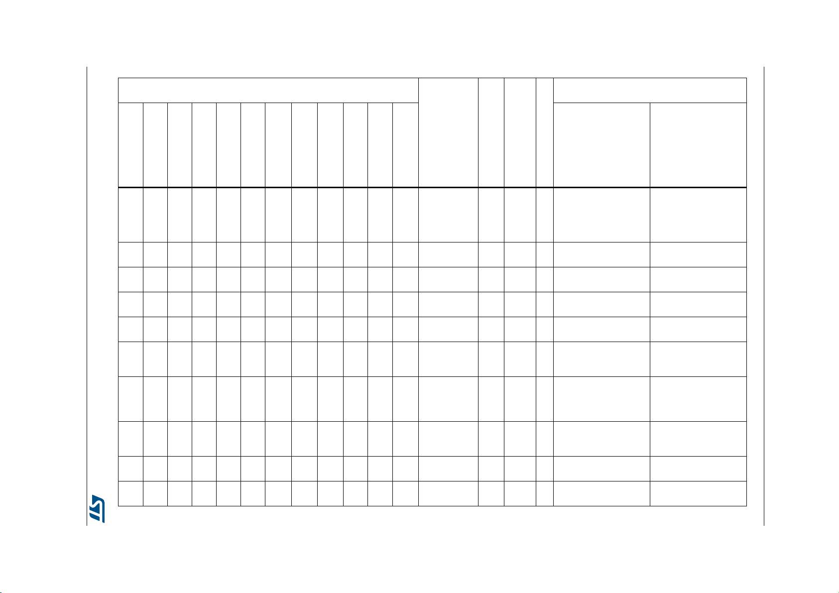
78/281 DS11585 Rev 11
Table 15. STM32L496xx pin definitions (continued)
Pinouts and pin description STM32L496xx
Pin Number
LQFP64
WLCSP100
LQFP64_SMPS
28 27 F5 J6 37 37 L6
------K6
------J7
-------
-------
------K7
------J8
------J9
------H9
------G9
WLCSP100_SMPS
LQFP100
UFBGA132
LQFP100_SMPS
Pin name
(function
Notes
after reset)
LQFP144
UFBGA132_SMPS
48 48 N5 N5 PB2 I/O FT_la -
L6
49 49 M5 M5 PF11 I/O FT - DCMI_D12, EVENTOUT -
K6
50 50 N6 N6 PF12 I/O FT - FMC_A6, EVENTOUT -
J7
51 51 - - VSS S - - - -
-
52 52 A8 A8 VDD S - - - -
-
53 53 M6 M6 PF13 I/O FT -
K7
54 54 L6 L6 PF14 I/O FT_fa -
J8
55 55 K6 K6 PF15 I/O FT_fa -
J9
56 56 J6 J6 PG0 I/O FT -
H9
57 57 H6 H6 PG1 I/O FT -
G9
LQFP144_SMPS
UFBGA169
UFBGA169_SMPS
Pin type
I/O structure
Alternate functions Additional functions
RTC_OUT,
LPTIM1_OUT,
I2C3_SMBA,
DFSDM1_CKIN0,
LCD_VLCD, EVENTOUT
I2C4_SMBA,
DFSDM1_DATIN6,
FMC_A7, EVENTOUT
I2C4_SCL,
DFSDM1_CKIN6,
TSC_G8_IO1, FMC_A8,
EVENTOUT
I2C4_SDA,
TSC_G8_IO2, FMC_A9,
EVENTOUT
TSC_G8_IO3, FMC_A10,
EVENTOUT
TSC_G8_IO4, FMC_A11,
EVENTOUT
Pin functions
COMP1_INP
-
-
-
-
-
Page 79

Table 15. STM32L496xx pin definitions (continued)
STM32L496xx Pinouts and pin description
DS11585 Rev 11 79/281
Pin Number
LQFP64
WLCSP100
LQFP64_SMPS
- - K6 K6 38 38 M7
- - K5 K5 39 39 L7
- - J5 J5 40 40 M8
------F6
------G6
- - H5 H5 41 41 L8
- - K4 K4 42 42 M9
WLCSP100_SMPS
LQFP100
UFBGA132
LQFP100_SMPS
Pin name
(function
Notes
after reset)
LQFP144
UFBGA132_SMPS
58 58 L7 L7 PE7 I/O FT -
M7
59 59 K7 K7 PE8 I/O FT -
L7
60 60 J7 J7 PE9 I/O FT -
M8
61 61 M7 M7 VSS S - - - -
F6
62 62 N7 N7 VDD S - - - -
G6
63 63 H7 H7 PE10 I/O FT -
L8
64 64 N8 N8 PE11 I/O FT -
M9
LQFP144_SMPS
UFBGA169
UFBGA169_SMPS
Pin type
I/O structure
Alternate functions Additional functions
TIM1_ETR,
DFSDM1_DATIN2,
FMC_D4, SAI1_SD_B,
EVENTOUT
TIM1_CH1N,
DFSDM1_CKIN2,
FMC_D5, SAI1_SCK_B,
EVENTOUT
TIM1_CH1,
DFSDM1_CKOUT,
FMC_D6, SAI1_FS_B,
EVENTOUT
TIM1_CH2N,
DFSDM1_DATIN4,
TSC_G5_IO1,
QUADSPI_CLK,
FMC_D7,
SAI1_MCLK_B,
EVENTOUT
TIM1_CH2,
DFSDM1_CKIN4,
TSC_G5_IO2,
QUADSPI_BK1_NCS,
FMC_D8, EVENTOUT
Pin functions
-
-
-
-
-
Page 80
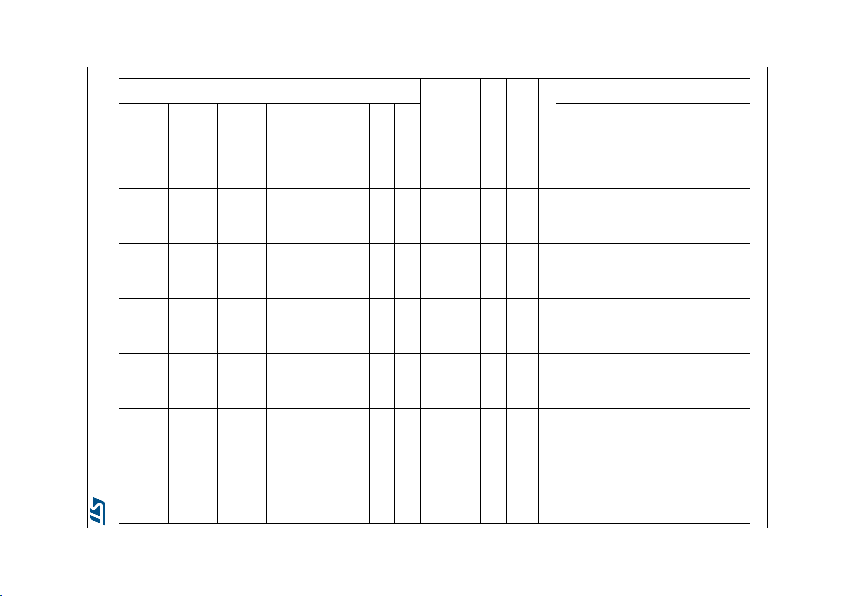
80/281 DS11585 Rev 11
Table 15. STM32L496xx pin definitions (continued)
Pinouts and pin description STM32L496xx
Pin Number
LQFP64
WLCSP100
LQFP64_SMPS
- - G5 J4 43 43 L9
- - G4 G5 44 44 M10
- - J4 G4 45 45 M11
- - H4 H4 46 46 M12
29 28 K3 K3 47 47 L10
WLCSP100_SMPS
LQFP100
LQFP100_SMPS
UFBGA132
Pin name
(function
after reset)
LQFP144
UFBGA132_SMPS
65 65 M8 M8 PE12 I/O FT -
L9
66 66 L8 L8 PE13 I/O FT -
M10
67 67 K8 K8 PE14 I/O FT -
M11
68 68 J8 J8 PE15 I/O FT -
M12
69 69 N9 N9 PB10 I/O FT_fl -
L10
LQFP144_SMPS
UFBGA169
UFBGA169_SMPS
Pin type
Notes
I/O structure
Pin functions
Alternate functions Additional functions
TIM1_CH3N, SPI1_NSS,
DFSDM1_DATIN5,
TSC_G5_IO3,
QUADSPI_BK1_IO0,
FMC_D9, EVENTOUT
TIM1_CH3, SPI1_SCK,
DFSDM1_CKIN5,
TSC_G5_IO4,
QUADSPI_BK1_IO1,
FMC_D10, EVENTOUT
TIM1_CH4, TIM1_BKIN2,
TIM1_BKIN2_COMP2,
SPI1_MISO,
QUADSPI_BK1_IO2,
FMC_D11, EVENTOUT
TIM1_BKIN,
TIM1_BKIN_COMP1,
SPI1_MOSI,
QUADSPI_BK1_IO3,
FMC_D12, EVENTOUT
TIM2_CH3, I2C4_SCL,
I2C2_SCL, SPI2_SCK,
DFSDM1_DATIN7,
USART3_TX,
LPUART1_RX,
TSC_SYNC,
QUADSPI_CLK,
LCD_SEG10,
COMP1_OUT,
SAI1_SCK_A,
EVENTOUT
-
-
-
-
-
Page 81

Table 15. STM32L496xx pin definitions (continued)
STM32L496xx Pinouts and pin description
DS11585 Rev 11 81/281
Pin Number
LQFP64
WLCSP100
LQFP64_SMPS
30 29 J3 J3 48 - L11
-30-K1-48-
-------
-------
-------
-------
-------
WLCSP100_SMPS
LQFP100
UFBGA132
LQFP100_SMPS
Pin name
(function
after reset)
LQFP144
UFBGA132_SMPS
70 - H8 H8 PB11 I/O FT_fl -
-
L11
- 70 - M10 VDD12 S - - - -
- - K9 K9 PH4 I/O FT_f - I2C2_SCL, EVENTOUT -
-
- - L9 L9 PH5 I/O FT_f -
-
- - N10 N10 PH8 I/O FT_f -
-
- - M9 M9 PH10 I/O FT -
-
- - M10 - PH11 I/O FT -
-
LQFP144_SMPS
UFBGA169
UFBGA169_SMPS
Pin type
Notes
I/O structure
Pin functions
Alternate functions Additional functions
TIM2_CH4, I2C4_SDA,
I2C2_SDA,
DFSDM1_CKIN7,
USART3_RX,
LPUART1_TX,
QUADSPI_BK1_NCS,
LCD_SEG11,
COMP2_OUT,
EVENTOUT
I2C2_SDA,
DCMI_PIXCLK,
EVENTOUT
I2C3_SDA,
DCMI_HSYNC,
EVENTOUT
TIM5_CH1, DCMI_D1,
EVENTOUT
TIM5_CH2, DCMI_D2,
EVENTOUT
-
-
-
-
-
-------
-------
- - M3 M3 VSS S - - - -
-
- - N3 N3 VDD S - - - -
-
Page 82

82/281 DS11585 Rev 11
Table 15. STM32L496xx pin definitions (continued)
Pinouts and pin description STM32L496xx
Pin Number
LQFP64
WLCSP100
LQFP64_SMPS
-------
31 31 K2 K2 49 49 F12
32 32 K1 J2 50 50 G12
-------
33 33 J1 J1 51 51 L12
WLCSP100_SMPS
LQFP100
UFBGA132
LQFP100_SMPS
Pin name
(function
Notes
after reset)
LQFP144
UFBGA132_SMPS
- - M11 M11 VSS S - - - -
-
71 71 L13 L13 VSS S - - - -
F12
72 72 L12 L12 VDD S - - - -
G12
--N11N11 VDD S --- -
-
73 73 N12 N12 PB12 I/O FT_l -
L12
LQFP144_SMPS
UFBGA169
UFBGA169_SMPS
Pin type
I/O structure
Alternate functions Additional functions
TIM1_BKIN,
TIM1_BKIN_COMP2,
I2C2_SMBA, SPI2_NSS,
DFSDM1_DATIN1,
USART3_CK,
LPUART1_RTS_DE,
TSC_G1_IO1,
CAN2_RX, LCD_SEG12,
SWPMI1_IO,
SAI2_FS_A,
TIM15_BKIN,
EVENTOUT
Pin functions
-
Page 83

Table 15. STM32L496xx pin definitions (continued)
STM32L496xx Pinouts and pin description
DS11585 Rev 11 83/281
Pin Number
LQFP64
WLCSP100
LQFP64_SMPS
34 34 J2 H2 52 52 K12
35 35 H2 H1 53 53 K11
36 36 H1 H3 54 54 K10
WLCSP100_SMPS
LQFP100
LQFP100_SMPS
UFBGA132
Pin name
(function
after reset)
LQFP144
UFBGA132_SMPS
74 74 N13 N13 PB13 I/O FT_fl -
K12
75 75 M13 M13 PB14 I/O FT_fl -
K11
76 76 M12 M12 PB15 I/O FT_l -
K10
LQFP144_SMPS
UFBGA169
UFBGA169_SMPS
Pin type
Notes
I/O structure
Pin functions
Alternate functions Additional functions
TIM1_CH1N, I2C2_SCL,
SPI2_SCK,
DFSDM1_CKIN1,
USART3_CTS,
LPUART1_CTS,
TSC_G1_IO2, CAN2_TX,
LCD_SEG13,
SWPMI1_TX,
SAI2_SCK_A,
TIM15_CH1N,
EVENTOUT
TIM1_CH2N,
TIM8_CH2N, I2C2_SDA,
SPI2_MISO,
DFSDM1_DATIN2,
USART3_RTS_DE,
TSC_G1_IO3,
LCD_SEG14,
SWPMI1_RX,
SAI2_MCLK_A,
TIM15_CH1, EVENTOUT
RTC_REFIN,
TIM1_CH3N,
TIM8_CH3N,
SPI2_MOSI,
DFSDM1_CKIN2,
TSC_G1_IO4,
LCD_SEG15,
SWPMI1_SUSPEND,
SAI2_SD_A,
TIM15_CH2, EVENTOUT
-
-
-
Page 84

84/281 DS11585 Rev 11
Table 15. STM32L496xx pin definitions (continued)
Pinouts and pin description STM32L496xx
Pin Number
LQFP64
WLCSP100
LQFP64_SMPS
- - H3 G3 55 55 K9
- - G2 G2 56 56 K8
- - G1 G1 57 57 J12
----5858J11
----5959J10
WLCSP100_SMPS
LQFP100
UFBGA132
LQFP100_SMPS
J12
J11
J10
Pin name
(function
after reset)
LQFP144
UFBGA132_SMPS
77 77 L11 L11 PD8 I/O FT_l -
K9
78 78 L10 L10 PD9 I/O FT_l -
K8
79 79 J13 J13 PD10 I/O FT_l -
80 80 K12 K12 PD11 I/O FT_l -
81 81 K11 K11 PD12 I/O FT_fl -
LQFP144_SMPS
UFBGA169
UFBGA169_SMPS
Pin type
Notes
I/O structure
Pin functions
Alternate functions Additional functions
USART3_TX,
DCMI_HSYNC,
LCD_SEG28, FMC_D13,
EVENTOUT
USART3_RX,
DCMI_PIXCLK,
LCD_SEG29, FMC_D14,
SAI2_MCLK_A,
EVENTOUT
USART3_CK,
TSC_G6_IO1,
LCD_SEG30, FMC_D15,
SAI2_SCK_A,
EVENTOUT
I2C4_SMBA,
USART3_CTS,
TSC_G6_IO2,
LCD_SEG31, FMC_A16,
SAI2_SD_A,
LPTIM2_ETR,
EVENTOUT
TIM4_CH1, I2C4_SCL,
USART3_RTS_DE,
TSC_G6_IO3,
LCD_SEG32, FMC_A17,
SAI2_FS_A,
LPTIM2_IN1,
EVENTOUT
-
-
-
-
-
Page 85

Table 15. STM32L496xx pin definitions (continued)
STM32L496xx Pinouts and pin description
DS11585 Rev 11 85/281
Pin Number
LQFP64
WLCSP100
LQFP64_SMPS
----6060H12
-------
--F1F1-- -
- - G3 F3 61 61 H11
- - F4 F2 62 62 H10
------G10
------F9
------F10
------E9
WLCSP100_SMPS
LQFP100
UFBGA132
LQFP100_SMPS
H12
H11
H10
G10
F10
Pin name
(function
Notes
after reset)
LQFP144
UFBGA132_SMPS
82 82 K13 K13 PD13 I/O FT_fl -
83 83 H12 H12 VSS S - - - -
-
84 84 H13 H13 VDD S - - - -
-
85 85 K10 K10 PD14 I/O FT_l -
86 86 H11 H11 PD15 I/O FT_l -
87 87 J12 J12 PG2 I/O FT_s -
88 88 J11 J11 PG3 I/O FT_s -
F9
89 89 J10 J10 PG4 I/O FT_s -
90 90 J9 J9 PG5 I/O FT_s -
E9
LQFP144_SMPS
UFBGA169
UFBGA169_SMPS
Pin type
I/O structure
Alternate functions Additional functions
TIM4_CH2, I2C4_SDA,
TSC_G6_IO4,
LCD_SEG33, FMC_A18,
LPTIM2_OUT,
EVENTOUT
TIM4_CH3,
LCD_SEG34, FMC_D0,
EVENTOUT
TIM4_CH4,
LCD_SEG35, FMC_D1,
EVENTOUT
SPI1_SCK, FMC_A12,
SAI2_SCK_B,
EVENTOUT
SPI1_MISO, FMC_A13,
SAI2_FS_B, EVENTOUT
SPI1_MOSI, FMC_A14,
SAI2_MCLK_B,
EVENTOUT
SPI1_NSS,
LPUART1_CTS,
FMC_A15, SAI2_SD_B,
EVENTOUT
Pin functions
-
-
-
-
-
-
-
Page 86

86/281 DS11585 Rev 11
Table 15. STM32L496xx pin definitions (continued)
Pinouts and pin description STM32L496xx
Pin Number
LQFP64
WLCSP100
LQFP64_SMPS
------G4
------H4
------J6
-------
-------
37 37 F2 F4 63 63 E12
38 38 F3 E4 64 64 E11
WLCSP100_SMPS
LQFP100
UFBGA132
LQFP100_SMPS
Pin name
(function
Notes
after reset)
LQFP144
UFBGA132_SMPS
91 91 G11 G11 PG6 I/O FT_s -
G4
92 92 H10 H10 PG7 I/O FT_fs -
H4
93 93 H9 H9 PG8 I/O FT_fs -
J6
94 94 F13 F13 VSS S - - - -
-
95 95 F12 F12 VDDIO2 S - - - -
-
96 96 F11 F11 PC6 I/O FT_l -
E12
97 97 G12 G12 PC7 I/O FT_l -
E11
LQFP144_SMPS
UFBGA169
UFBGA169_SMPS
Pin type
I/O structure
Alternate functions Additional functions
I2C3_SMBA,
LPUART1_RTS_DE,
EVENTOUT
I2C3_SCL,
LPUART1_TX, FMC_INT,
SAI1_MCLK_A,
EVENTOUT
I2C3_SDA,
LPUART1_RX,
EVENTOUT
TIM3_CH1, TIM8_CH1,
DFSDM1_CKIN3,
TSC_G4_IO1, DCMI_D0,
LCD_SEG24,
SDMMC1_D6,
SAI2_MCLK_A,
EVENTOUT
TIM3_CH2, TIM8_CH2,
DFSDM1_DATIN3,
TSC_G4_IO2, DCMI_D1,
LCD_SEG25,
SDMMC1_D7,
SAI2_MCLK_B,
EVENTOUT
Pin functions
-
-
-
-
-
Page 87

Table 15. STM32L496xx pin definitions (continued)
STM32L496xx Pinouts and pin description
DS11585 Rev 11 87/281
Pin Number
LQFP64
WLCSP100
LQFP64_SMPS
39 39 E1 E1 65 65 E10
40 40 E2 E2 66 66 D12
41 41 E3 E3 67 67 D11
42 42 D3 D3 68 68 D10
WLCSP100_SMPS
LQFP100
LQFP100_SMPS
UFBGA132
Pin name
(function
after reset)
LQFP144
UFBGA132_SMPS
98 98 G10 G10 PC8 I/O FT_l -
E10
99 99 G9 G9 PC9 I/O FT_fl -
D12
100 100 G8 G8 PA8 I/O FT_l -
D11
101 101 F10 F10 PA9 I/O FT_lu -
D10
LQFP144_SMPS
UFBGA169
UFBGA169_SMPS
Pin type
Notes
I/O structure
Pin functions
Alternate functions Additional functions
TIM3_CH3, TIM8_CH3,
TSC_G4_IO3, DCMI_D2,
LCD_SEG26,
SDMMC1_D0,
EVENTOUT
TIM8_BKIN2, TIM3_CH4,
TIM8_CH4, DCMI_D3,
I2C3_SDA,
TSC_G4_IO4,
OTG_FS_NOE,
LCD_SEG27,
SDMMC1_D1,
SAI2_EXTCLK,
TIM8_BKIN2_COMP1,
EVENTOUT
MCO, TIM1_CH1,
USART1_CK,
OTG_FS_SOF,
LCD_COM0,
SWPMI1_IO,
SAI1_SCK_A,
LPTIM2_OUT,
EVENTOUT
TIM1_CH2, SPI2_SCK,
DCMI_D0, USART1_TX,
LCD_COM1,
SAI1_FS_A,
TIM15_BKIN,
EVENTOUT
-
-
-
OTG_FS_VBUS
Page 88

88/281 DS11585 Rev 11
Table 15. STM32L496xx pin definitions (continued)
Pinouts and pin description STM32L496xx
Pin Number
LQFP64
WLCSP100
LQFP64_SMPS
43 43 D2 D2 69 69 C12
44 44 D1 D1 70 70 B12
45 45 C1 C1 71 71 A12
46 46 C2 C2 72 72 A11
WLCSP100_SMPS
LQFP100
LQFP100_SMPS
UFBGA132
Pin name
(function
after reset)
LQFP144
UFBGA132_SMPS
102 102 F9 F9 PA10 I/O FT_lu -
C12
103 103 E13 E13 PA11 I/O FT_u -
B12
104 104 D13 D13 PA12 I/O FT_u -
A12
105 105 A11 A11
A11
LQFP144_SMPS
UFBGA169
UFBGA169_SMPS
PA1 3 (J TMS/
SWDIO)
Pin type
I/O FT
Notes
I/O structure
(4)
Pin functions
Alternate functions Additional functions
TIM1_CH3, DCMI_D1,
USART1_RX,
OTG_FS_ID,
LCD_COM2,
SAI1_SD_A,
TIM17_BKIN,
EVENTOUT
TIM1_CH4, TIM1_BKIN2,
SPI1_MISO,
USART1_CTS,
CAN1_RX,
OTG_FS_DM,
TIM1_BKIN2_COMP1,
EVENTOUT
TIM1_ETR, SPI1_MOSI,
USART1_RTS_DE,
CAN1_TX, OTG_FS_DP,
EVENTOUT
JTMS/SWDIO, IR_OUT,
OTG_FS_NOE,
SWPMI1_TX,
SAI1_SD_B, EVENTOUT
-
-
-
-
47 47 B1 B1 - - -
48 48 A1 A1 73 73 C11
----7474F11
---- VSS S --- -
-
106 106 E12 E12 VDDUSB S - - - -
C11
107 107 C12 C12 VSS S - - - -
F11
Page 89

Table 15. STM32L496xx pin definitions (continued)
STM32L496xx Pinouts and pin description
DS11585 Rev 11 89/281
Pin Number
LQFP64
WLCSP100
LQFP64_SMPS
----7575G11
-------
-------
-------
-------
-------
-------
-------
WLCSP100_SMPS
LQFP100
UFBGA132
LQFP100_SMPS
G11
Pin name
(function
Notes
after reset)
LQFP144
UFBGA132_SMPS
108 108 C13 C13 VDD S - - - -
- - E11 E11 PH6 I/O FT -
-
- - D12 D12 PH7 I/O FT_f -
-
- - D11 D11 PH9 I/O FT -
-
- - B13 B13 PH12 I/O FT -
-
- - A13 A13 PH14 I/O FT -
-
- - B12 B12 PH15 I/O FT -
-
- - A12 A12 PI0 I/O FT -
-
LQFP144_SMPS
UFBGA169
UFBGA169_SMPS
Pin type
I/O structure
Alternate functions Additional functions
I2C2_SMBA, DCMI_D8,
EVENTOUT
I2C3_SCL, DCMI_D9,
EVENTOUT
I2C3_SMBA, DCMI_D0,
EVENTOUT
TIM5_CH3, DCMI_D3,
EVENTOUT
TIM8_CH2N, DCMI_D4,
EVENTOUT
TIM8_CH3N, DCMI_D11,
EVENTOUT
TIM5_CH4, SPI2_NSS,
DCMI_D13, EVENTOUT
Pin functions
-
-
-
-
-
-
-
-------
-------
-------
-------
-------
- - C11 C11 PI8 I/O FT - DCMI_D12, EVENTOUT -
-
- - B11 B11 PI1 I/O FT -
-
- - B10 B10 PI2 I/O FT -
-
- - C10 C10 PI3 I/O FT -
-
- - D10 D10 PI4 I/O FT -
-
SPI2_SCK, DCMI_D8,
EVENTOUT
TIM8_CH4, SPI2_MISO,
DCMI_D9, EVENTOUT
TIM8_ETR, SPI2_MOSI,
DCMI_D10, EVENTOUT
TIM8_BKIN, DCMI_D5,
EVENTOUT
-
-
-
-
Page 90
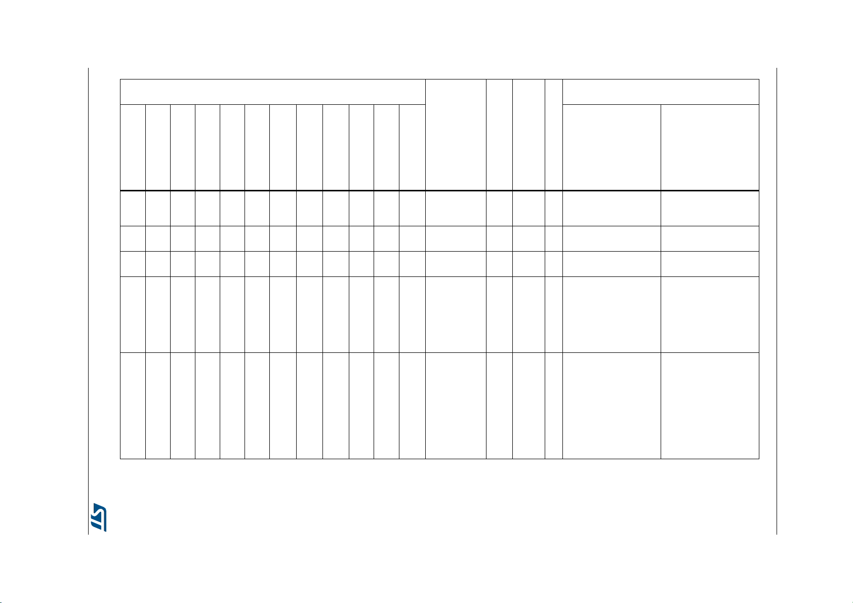
90/281 DS11585 Rev 11
Table 15. STM32L496xx pin definitions (continued)
Pinouts and pin description STM32L496xx
Pin Number
LQFP64
WLCSP100
LQFP64_SMPS
-------
-------
-------
49 49 B2 B2 76 76 A10
50 50 A2 A2 77 77 A9
WLCSP100_SMPS
LQFP100
UFBGA132
LQFP100_SMPS
Pin name
(function
after reset)
LQFP144
UFBGA132_SMPS
- - E10 E10 PI5 I/O FT -
-
- - C9 C9 PH13 I/O FT -
-
- - B9 B9 PI6 I/O FT -
-
109 109 A10 A10
A10
110 110 A9 A9 PA15 (JTDI) I/O FT_l
A9
LQFP144_SMPS
UFBGA169
UFBGA169_SMPS
PA14 (JTCK/
SWCLK)
Pin type
I/O FT
Notes
I/O structure
(4)
(4)
Pin functions
Alternate functions Additional functions
TIM8_CH1,
DCMI_VSYNC,
EVENTOUT
TIM8_CH1N, CAN1_TX,
EVENTOUT
TIM8_CH2, DCMI_D6,
EVENTOUT
JTCK/SWCLK,
LPTIM1_OUT,
I2C1_SMBA,
I2C4_SMBA,
OTG_FS_SOF,
SWPMI1_RX,
SAI1_FS_B, EVENTOUT
JTDI, TIM2_CH1,
TIM2_ETR,
USART2_RX,
SPI1_NSS, SPI3_NSS,
USART3_RTS_DE,
UART4_RTS_DE,
TSC_G3_IO1,
LCD_SEG17,
SWPMI1_SUSPEND,
SAI2_FS_B, EVENTOUT
-
-
-
-
-
Page 91

Table 15. STM32L496xx pin definitions (continued)
STM32L496xx Pinouts and pin description
DS11585 Rev 11 91/281
Pin Number
LQFP64
WLCSP100
LQFP64_SMPS
51 51 D4 C3 78 78 B11
52 52 C3 D4 79 79 C10
53 53 C4 C4 80 80 B10
- - B3 B3 81 81 C9
WLCSP100_SMPS
LQFP100
LQFP100_SMPS
UFBGA132
Pin name
(function
after reset)
LQFP144
UFBGA132_SMPS
111 111 D9 D9 P C10 I/ O F T_l -
B11
112 112 E9 E9 PC11 I/O FT_l -
C10
113 113 F8 F8 PC12 I/O FT_l -
B10
114 114 B8 B8 PD0 I/O FT -
C9
LQFP144_SMPS
UFBGA169
UFBGA169_SMPS
Pin type
Notes
I/O structure
Pin functions
Alternate functions Additional functions
TRACED1, SPI3_SCK,
USART3_TX,
UART4_TX,
TSC_G3_IO2, DCMI_D8,
LCD_COM4/LCD_SEG2
8/LCD_SEG40,
SDMMC1_D2,
SAI2_SCK_B,
EVENTOUT
QUADSPI_BK2_NCS,
SPI3_MISO,
USART3_RX,
UART4_RX,
TSC_G3_IO3, DCMI_D4,
LCD_COM5/LCD_SEG2
9/LCD_SEG41,
SDMMC1_D3,
SAI2_MCLK_B,
EVENTOUT
TRACED3, SPI3_MOSI,
USART3_CK,
UART5_TX,
TSC_G3_IO4, DCMI_D9,
LCD_COM6/LCD_SEG3
0/LCD_SEG42,
SDMMC1_CK,
SAI2_SD_B, EVENTOUT
SPI2_NSS,
DFSDM1_DATIN7,
CAN1_RX, FMC_D2,
EVENTOUT
-
-
-
-
Page 92

92/281 DS11585 Rev 11
Table 15. STM32L496xx pin definitions (continued)
Pinouts and pin description STM32L496xx
Pin Number
LQFP64
WLCSP100
LQFP64_SMPS
- - A3 A3 82 82 B9
54 - E4 D5 83 83 C8
----8484B8
- - B4 C5 85 85 B7
- - E5 B4 86 86 A6
WLCSP100_SMPS
LQFP100
UFBGA132
LQFP100_SMPS
Pin name
(function
after reset)
LQFP144
UFBGA132_SMPS
115 115 C8 C8 PD1 I/O FT -
B9
116 116 D8 D8 PD2 I/O FT_l -
C8
117 117 E8 E8 PD3 I/O FT -
B8
118 118 C7 C7 PD4 I/O FT -
B7
119 119 D7 D7 PD5 I/O FT -
A6
LQFP144_SMPS
UFBGA169
UFBGA169_SMPS
Pin type
Notes
I/O structure
Pin functions
Alternate functions Additional functions
SPI2_SCK,
DFSDM1_CKIN7,
CAN1_TX, FMC_D3,
EVENTOUT
TRACED2, TIM3_ETR,
USART3_RTS_DE,
UART5_RX, TSC_SYNC,
DCMI_D11,
LCD_COM7/LCD_SEG3
1/LCD_SEG43,
SDMMC1_CMD,
EVENTOUT
SPI2_SCK, DCMI_D5,
SPI2_MISO,
DFSDM1_DATIN0,
USART2_CTS,
QUADSPI_BK2_NCS,
FMC_CLK, EVENTOUT
SPI2_MOSI,
DFSDM1_CKIN0,
USART2_RTS_DE,
QUADSPI_BK2_IO0,
FMC_NOE, EVENTOUT
USART2_TX,
QUADSPI_BK2_IO1,
FMC_NWE, EVENTOUT
-
-
-
-
-
-------
--A4A4-- -
120 120 - - VSS S - - - -
-
121 121 - - VDD S - - - -
-
Page 93
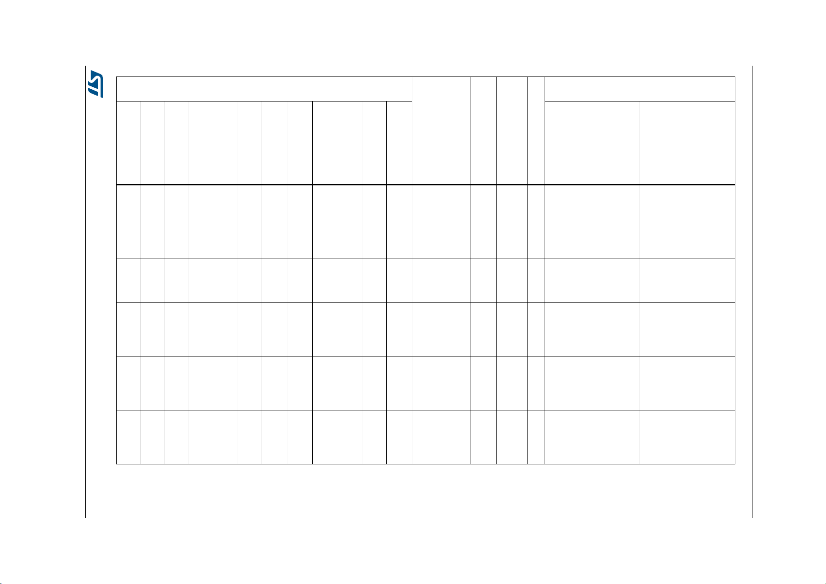
Table 15. STM32L496xx pin definitions (continued)
STM32L496xx Pinouts and pin description
DS11585 Rev 11 93/281
Pin Number
LQFP64
WLCSP100
LQFP64_SMPS
- - D5 B5 87 87 B6
- - C5 C6 88 88 A5
- - B5 D6 - - D9
--A5A5--D8
--D6E5--G3
WLCSP100_SMPS
LQFP100
UFBGA132
LQFP100_SMPS
Pin name
(function
after reset)
LQFP144
UFBGA132_SMPS
122 122 E7 E7 PD6 I/O FT -
B6
123 123 F7 F7 PD7 I/O FT -
A5
124 124 B7 B7 PG9 I/O FT_s -
D9
125 125 D6 D6 PG10 I/O FT_s -
D8
126 126 E6 E6 PG11 I/O FT_s -
G3
LQFP144_SMPS
UFBGA169
UFBGA169_SMPS
Pin type
Notes
I/O structure
Pin functions
Alternate functions Additional functions
DCMI_D10,
QUADSPI_BK2_IO1,
DFSDM1_DATIN1,
USART2_RX,
QUADSPI_BK2_IO2,
FMC_NWAIT,
SAI1_SD_A, EVENTOUT
DFSDM1_CKIN1,
USART2_CK,
QUADSPI_BK2_IO3,
FMC_NE1, EVENTOUT
SPI3_SCK, USART1_TX,
FMC_NCE/FMC_NE2,
SAI2_SCK_A,
TIM15_CH1N,
EVENTOUT
LPTIM1_IN1,
SPI3_MISO,
USART1_RX, FMC_NE3,
SAI2_FS_A,
TIM15_CH1, EVENTOUT
LPTIM1_IN2,
SPI3_MOSI,
USART1_CTS,
SAI2_MCLK_A,
TIM15_CH2, EVENTOUT
-
-
-
-
-
Page 94
94/281 DS11585 Rev 11
Table 15. STM32L496xx pin definitions (continued)
Pinouts and pin description STM32L496xx
Pin Number
Pin name
(function
after reset)
LQFP64
WLCSP100
LQFP64_SMPS
--B6B6--D7D7127 127 F6 F6 PG12 I/O FT_s -
------C7
------C6
------F7
--A6A6--G7
------K1
55 54 C6 F5 89 89 A8
WLCSP100_SMPS
LQFP100
UFBGA132
LQFP100_SMPS
C7
-
F7
G7
K1
A8
LQFP144
UFBGA132_SMPS
128 128 G7 G7 PG13 I/O FT_fs -
129 129 G6 G6 PG14 I/O FT_fs -
130 130 A7 A7 VSS S - - - -
131 131 B6 B6 VDDIO2 S - - - -
132 - C6 - PG15 I/O FT_s -
133 132 A6 A6
LQFP144_SMPS
UFBGA169
UFBGA169_SMPS
PB3
(JTDO/TRACE
SWO)
Pin type
I/O structure
I/O FT_la
Pin functions
Notes
Alternate functions Additional functions
LPTIM1_ETR,
SPI3_NSS,
USART1_RTS_DE,
FMC_NE4, SAI2_SD_A,
EVENTOUT
I2C1_SDA, USART1_CK,
FMC_A24, EVENTOUT
I2C1_SCL, FMC_A25,
EVENTOUT
LPTIM1_OUT,
I2C1_SMBA, DCMI_D13,
EVENTOUT
JTDO/TRACESWO,
TIM2_CH2, SPI1_SCK,
SPI3_SCK,
USART1_RTS_DE,
(4)
OTG_FS_CRS_SYNC,
LCD_SEG7,
SAI1_SCK_B,
EVENTOUT
-
-
-
-
COMP2_INM
Page 95

Table 15. STM32L496xx pin definitions (continued)
STM32L496xx Pinouts and pin description
DS11585 Rev 11 95/281
Pin Number
LQFP64
WLCSP100
LQFP64_SMPS
56 55 C7 E6 90 90 A7
57 56 B7 C7 91 91 C5
58 57 A7 A7 92 92 B5
WLCSP100_SMPS
LQFP100
LQFP100_SMPS
UFBGA132
Pin name
(function
after reset)
LQFP144
UFBGA132_SMPS
134 133 A5 A5 PB4 (NJTRST) I/O FT_fla
A7
135 134 B5 B5 PB5 I/O FT_la -
C5
136 135 C5 C5 PB6 I/O FT_fa -
B5
LQFP144_SMPS
UFBGA169
UFBGA169_SMPS
Pin type
Notes
I/O structure
(4)
Pin functions
Alternate functions Additional functions
NJTRST, TIM3_CH1,
I2C3_SDA, SPI1_MISO,
SPI3_MISO,
USART1_CTS,
UART5_RTS_DE,
TSC_G2_IO1,
DCMI_D12, LCD_SEG8,
SAI1_MCLK_B,
TIM17_BKIN,
EVENTOUT
LPTIM1_IN1, TIM3_CH2,
CAN2_RX, I2C1_SMBA,
SPI1_MOSI, SPI3_MOSI,
USART1_CK,
UART5_CTS,
TSC_G2_IO2,
DCMI_D10, LCD_SEG9,
COMP2_OUT,
SAI1_SD_B,
TIM16_BKIN,
EVENTOUT
LPTIM1_ETR,
TIM4_CH1, TIM8_BKIN2,
I2C1_SCL, I2C4_SCL,
DFSDM1_DATIN5,
USART1_TX, CAN2_TX,
TSC_G2_IO3, DCMI_D5,
TIM8_BKIN2_COMP2,
SAI1_FS_B,
TIM16_CH1N,
EVENTOUT
COMP2_INP
-
COMP2_INP
Page 96

96/281 DS11585 Rev 11
Table 15. STM32L496xx pin definitions (continued)
Pinouts and pin description STM32L496xx
Pin Number
LQFP64
WLCSP100
LQFP64_SMPS
59 58 D7 B7 93 93 B4
60 59 E6 D7 94 94 A4
61 60 B8 B8 95 95 A3
62 61 A8 A8 96 96 B3
WLCSP100_SMPS
LQFP100
LQFP100_SMPS
UFBGA132
Pin name
(function
Notes
after reset)
LQFP144
UFBGA132_SMPS
137 136 D5 D5 PB7 I/O FT_fla -
B4
138 137 E5 E5 PH3-BOOT0 I/O FT - EVENTOUT -
A4
139 138 C4 C4 PB8 I/O FT_fl -
A3
140 139 D4 D4 PB9 I/O FT_fl -
B3
LQFP144_SMPS
UFBGA169
UFBGA169_SMPS
Pin type
I/O structure
Alternate functions Additional functions
LPTIM1_IN2, TIM4_CH2,
TIM8_BKIN, I2C1_SDA,
I2C4_SDA,
DFSDM1_CKIN5,
USART1_RX,
UART4_CTS,
TSC_G2_IO4,
DCMI_VSYNC,
LCD_SEG21, FMC_NL,
TIM8_BKIN_COMP1,
TIM17_CH1N,
EVENTOUT
TIM4_CH3, I2C1_SCL,
DFSDM1_DATIN6,
CAN1_RX, DCMI_D6,
LCD_SEG16,
SDMMC1_D4,
SAI1_MCLK_A,
TIM16_CH1, EVENTOUT
IR_OUT, TIM4_CH4,
I2C1_SDA, SPI2_NSS,
DFSDM1_CKIN6,
CAN1_TX, DCMI_D7,
LCD_COM3,
SDMMC1_D5,
SAI1_FS_A,
TIM17_CH1, EVENTOUT
Pin functions
COMP2_INM, PVD_IN
-
-
-62---- -
C6
- - - C6 VDD12 S - - - -
Page 97

Table 15. STM32L496xx pin definitions (continued)
STM32L496xx Pinouts and pin description
DS11585 Rev 11 97/281
Pin Number
Pin name
(function
after reset)
LQFP64
WLCSP100
LQFP64_SMPS
----9797C3C3141 140 A4 A4 PE0 I/O FT_l -
----98-A2
---A9-98-
63 63 A9 B9 99 99 D3
64 64 A10 A10 100 100 C4
-------
-------
WLCSP100_SMPS
LQFP100
UFBGA132
LQFP100_SMPS
A2
-
D3
C4
-
-
LQFP144
UFBGA132_SMPS
142 141 B4 B4 PE1 I/O FT_l -
- 142 - - VDD12 S - - - -
143 143 B3 B3 VSS S - - - -
144 144 A3 A3 VDD S - - - -
- - C2 C2 VSS S - - - -
- - C1 C1 VDD S - - - -
LQFP144_SMPS
UFBGA169
UFBGA169_SMPS
Pin type
I/O structure
Pin functions
Notes
Alternate functions Additional functions
TIM4_ETR, DCMI_D2,
LCD_SEG36,
FMC_NBL0,
TIM16_CH1, EVENTOUT
DCMI_D3, LCD_SEG37,
FMC_NBL1,
TIM17_CH1, EVENTOUT
-
-
-------
-------
-------
-------
- - A2 A2 PH2 I/O FT -
-
-
-
-
--
--
--
B2 B2 PI7 I/O FT
B1 B1 PI9 I/O FT
A1 A1 PI10 I/O FT
QUADSPI_BK2_IO0,
EVENTOUT
TIM8_CH3, DCMI_D7,
EVENTOUT
CAN1_RX, EVENTOUT
-
EVENTOUT
-
-
-
-
-
Page 98

98/281 DS11585 Rev 11
1. PC13, PC14 and PC15 are supplied through the power switch. Since the switch only sinks a limited amount of current(3 mA), the use of GPIOs PC13 to PC15 in output
mode is limited:
- The speed should not exceed 2 MHz with a maximum load of 30 pF.
- These GPIOs must not be used as current sources (e.g. to drive an LED).
2. After a Backup domain power-up, PC13, PC14 and PC15 operate as GPIOs. Their function then depends on the content of the RTC registers which are not reset by the
system reset. For details on how to manage these GPIOs, refer to the Backup domain and RTC register descriptions in the RM0351 reference manual.
3. OPAMPx_VINM pins are not available as additional functions on pins PA1 and PA7 on UFBGA packages. On UFBGA packages, use the OPAMPx_VINM dedicated pins
available on M3 and M4 balls.
4. After reset, these pins are configured as JTAG/SW debug alternate functions, and the internal pull-up on PA15, PA13, PB4 pins and the internal pull-down on PA14 pin are
activated.
Pinouts and pin description STM32L496xx
Page 99

Table 16. Alternate function AF0 to AF7
(1)
STM32L496xx Pinouts and pin description
AF0 AF1 AF2 AF3 AF4 AF5 AF6 AF7
DS11585 Rev 11 99/281
Port A
Port
SYS_AF
TIM1/2/5/8/
LPTIM1
TIM1/2/3/4/5
SPI2/USART2/
CAN2/TIM8/
QUADSPI
I2C1/2/3/4/
DCMI
SPI1/2/DCMI/
QUADSPI
SPI3/I2C3/
DFSDM/
COMP1/
QUADSPI
USART1/2/3
PA0 - TIM2_CH1 TIM5_CH1 TIM8_ETR - - - USART2_CTS
PA1 - TIM2_CH2 TIM5_CH2 - I2C1_SMBA SPI1_SCK -
USART2_RTS_
DE
PA2 - TIM2_CH3 TIM5_CH3 - - - - USART2_TX
PA3 - TIM2_CH4 TIM5_CH4 - - - - USART2_RX
PA4-----SPI1_NSSSPI3_NSSUSART2_CK
PA5 - TIM2_CH1 TIM2_ETR TIM8_CH1N - SPI1_SCK - -
PA6 - TIM1_BKIN TIM3_CH1 TIM8_BKIN DCMI_PIXCLK SPI1_MISO - USART3_CTS
PA7 - TIM1_CH1N TIM3_CH2 TIM8_CH1N I2C3_SCL SPI1_MOSI - -
PA8 MCO TIM1_CH1 - - - - - USART1_CK
PA9 - TIM1_CH2 - SPI2_SCK - DCMI_D0 - USART1_TX
PA10 - TIM1_CH3 - - - DCMI_D1 - USART1_RX
PA11 - TIM1_CH4 TIM1_BKIN2 - - SPI1_MISO - USART1_CTS
PA12 - TIM1_ETR - - - SPI1_MOSI -
USART1_RTS_
PA13 JTMS/SWDIO IR_OUT - - - - - -
PA14 JTCK/SWCLK LPTIM1_OUT - - I2C1_SMBA I2C4_SMBA - -
PA15 JTDI TIM2_CH1 TIM2_ETR USART2_RX - SPI1_NSS SPI3_NSS
USART3_RTS_
DE
DE
Page 100

100/281 DS11585 Rev 11
AF0 AF1 AF2 AF3 AF4 AF5 AF6 AF7
Table 16. Alternate function AF0 to AF7
(1)
(continued)
Pinouts and pin description STM32L496xx
Port B
Port
SYS_AF
PB0 - TIM1_CH2N TIM3_CH3 TIM8_CH2N - SPI1_NSS - USART3_CK
PB1 - TIM1_CH3N TIM3_CH4 TIM8_CH3N - -
PB2 RTC_OUT LPTIM1_OUT - - I2C3_SMBA - DFSDM1_CKIN0 -
PB3
PB4 NJTRST - TIM3_CH1 - I2C3_SDA SPI1_MISO SPI3_MISO USART1_CTS
PB5 - LPTIM1_IN1 TIM3_CH2 CAN2_RX I2C1_SMBA SPI1_MOSI SPI3_MOSI USART1_CK
PB6 - LPTIM1_ETR TIM4_CH1 TIM8_BKIN2 I2C1_SCL I2C4_SCL
PB7 - LPTIM1_IN2 TIM4_CH2 TIM8_BKIN I2C1_SDA I2C4_SDA DFSDM1_CKIN5 USART1_RX
PB8 - - TIM4_CH3 - I2C1_SCL -
PB9 - IR_OUT TIM4_CH4 - I2C1_SDA SPI2_NSS DFSDM1_CKIN6 -
PB10 - TIM2_CH3 - I2C4_SCL I2C2_SCL SPI2_SCK
JTDO/
TRACESWO
TIM1/2/5/8/
LPTIM1
TIM2_CH2 - - - SPI1_SCK SPI3_SCK
TIM1/2/3/4/5
SPI2/USART2/
CAN2/TIM8/
QUADSPI
I2C1/2/3/4/
DCMI
SPI1/2/DCMI/
QUADSPI
SPI3/I2C3/
DFSDM/
COMP1/
QUADSPI
DFSDM1_
DATIN0
DFSDM1_
DATIN5
DFSDM1_
DATIN6
DFSDM1_
DATIN7
USART1/2/3
USART3_RTS_
USART1_RTS_
USART1_TX
USART3_TX
DE
DE
-
PB11 - TIM2_CH4 - I2C4_SDA I2C2_SDA - DFSDM1_CKIN7 USART3_RX
PB12 - TIM1_BKIN -
PB13 - TIM1_CH1N - - I2C2_SCL SPI2_SCK DFSDM1_CKIN1 USART3_CTS
PB14 - TIM1_CH2N - TIM8_CH2N I2C2_SDA SPI2_MISO
PB15 RTC_REFIN TIM1_CH3N - TIM8_CH3N - SPI2_MOSI DFSDM1_CKIN2 -
TIM1_BKIN_
COMP2
I2C2_SMBA SPI2_NSS
DFSDM1_
DATIN1
DFSDM1_
DATIN2
USART3_CK
USART3_RTS_
DE
 Loading...