

Page 1
UM1879
User manual
Discovery kit with STM32L476VG MCU
Introduction
The STM32L476 Discovery kit (32L476GDISCOVERY) helps the user to discover the
STM32L4 ultra-low-power features and to develop and share applications.
It is based on the STM32L476VGT6 microcontroller with three I2Cs, three SPIs, six
USARTs, CAN, SWPMI, two SAIs, 12-bit ADCs, 12-bit DAC, LCD driver, internal 128
of SRAM and 1
controller, FMC, JTAG debugging support.
The 32L476GDISCOVERY includes an ST-LINK/V2-1 embedded debugging tool interface,
LCD (24 segments, 4 commons), LEDs, push-button, joystick, USB OTG FS, audio DAC,
MEMS (microphone, 3-axis gyroscope, 6-axis compass), Quad-SPI Flash memory,
embedded ammeter measuring STM32 consumption in low-power mode.
External boards can be connected through the extension and probing connectors.
Mbyte of Flash memory, Quad-SPI, touch sensing, USB OTG FS, LCD
Kbytes
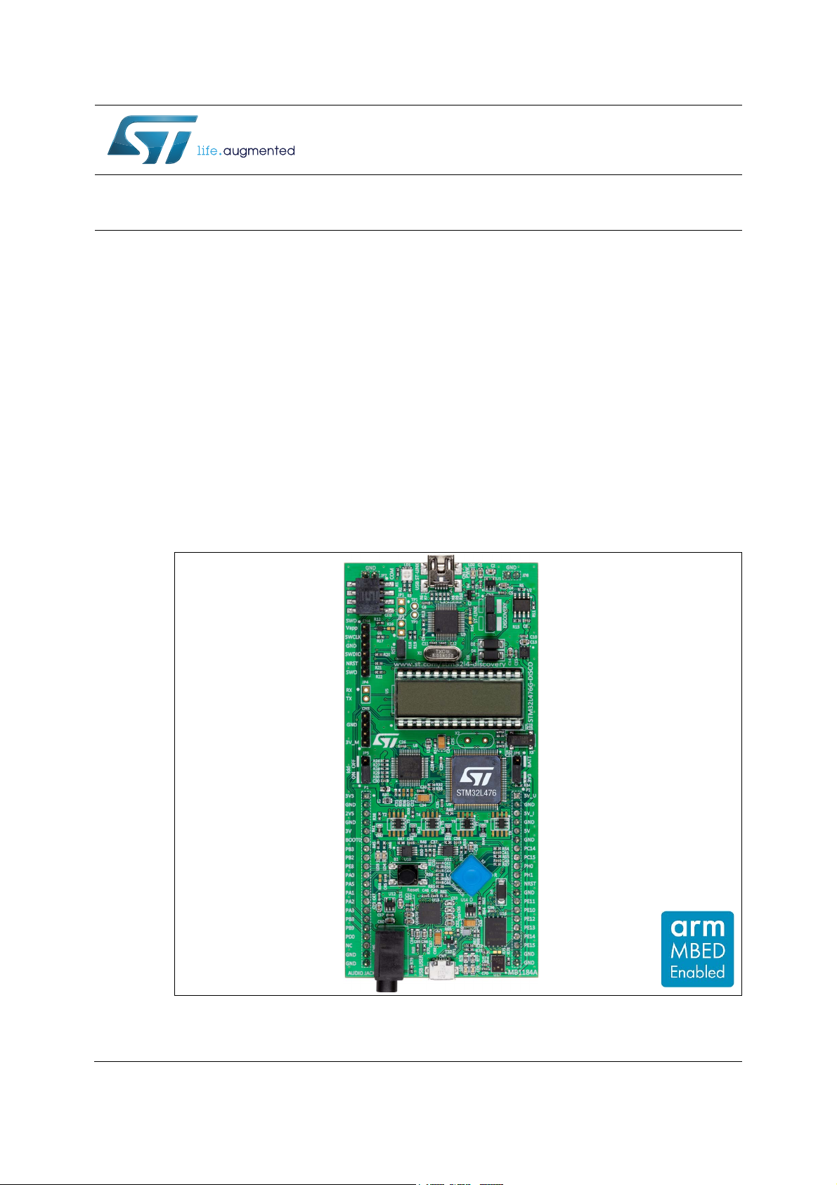
Figure 1. STM32L476 Discovery board
Picture is not contractual.
June 2018 UM1879 Rev 4 1/41
www.st.com
1
Page 2

Contents UM1879
Contents
1 Features . . . . . . . . . . . . . . . . . . . . . . . . . . . . . . . . . . . . . . . . . . . . . . . . . . . 6
2 Product marking . . . . . . . . . . . . . . . . . . . . . . . . . . . . . . . . . . . . . . . . . . . . 7
3 System requirements . . . . . . . . . . . . . . . . . . . . . . . . . . . . . . . . . . . . . . . . 7
4 Development toolchains . . . . . . . . . . . . . . . . . . . . . . . . . . . . . . . . . . . . . . 7
5 Demonstration software . . . . . . . . . . . . . . . . . . . . . . . . . . . . . . . . . . . . . . 8
6 Ordering information . . . . . . . . . . . . . . . . . . . . . . . . . . . . . . . . . . . . . . . . 8
7 Delivery recommendations . . . . . . . . . . . . . . . . . . . . . . . . . . . . . . . . . . . 8
8 Conventions . . . . . . . . . . . . . . . . . . . . . . . . . . . . . . . . . . . . . . . . . . . . . . . . 8
9 Bootloader limitations . . . . . . . . . . . . . . . . . . . . . . . . . . . . . . . . . . . . . . . 9
10 Hardware layout and configuration . . . . . . . . . . . . . . . . . . . . . . . . . . . . 10
10.1 Embedded ST-LINK/V2-1 . . . . . . . . . . . . . . . . . . . . . . . . . . . . . . . . . . . . . 13
10.1.1 Drivers . . . . . . . . . . . . . . . . . . . . . . . . . . . . . . . . . . . . . . . . . . . . . . . . . . 13
10.1.2 ST-LINK/V2-1 firmware upgrade . . . . . . . . . . . . . . . . . . . . . . . . . . . . . . 14
10.1.3 Using ST-LINK/V2-1 to program/debug the STM32L476VGT6
on board . . . . . . . . . . . . . . . . . . . . . . . . . . . . . . . . . . . . . . . . . . . . . . . . . 14
10.1.4 Using ST-LINK/V2-1 to program/debug an external STM32 application
board . . . . . . . . . . . . . . . . . . . . . . . . . . . . . . . . . . . . . . . . . . . . . . . . . . . 15
10.2 Power supply . . . . . . . . . . . . . . . . . . . . . . . . . . . . . . . . . . . . . . . . . . . . . . 16
10.3 Clock source . . . . . . . . . . . . . . . . . . . . . . . . . . . . . . . . . . . . . . . . . . . . . . . 18
10.4 Reset source . . . . . . . . . . . . . . . . . . . . . . . . . . . . . . . . . . . . . . . . . . . . . . 18
10.5 User interface: LCD, joystick, LEDs . . . . . . . . . . . . . . . . . . . . . . . . . . . . . 19
10.6 Boot0 configuration . . . . . . . . . . . . . . . . . . . . . . . . . . . . . . . . . . . . . . . . . 19
10.7 Quad-SPI NOR Flash memory . . . . . . . . . . . . . . . . . . . . . . . . . . . . . . . . . 19
10.8 USB OTG FS . . . . . . . . . . . . . . . . . . . . . . . . . . . . . . . . . . . . . . . . . . . . . . 19
10.9 USART configuration . . . . . . . . . . . . . . . . . . . . . . . . . . . . . . . . . . . . . . . . 20
10.10 Audio DAC and MEMS microphone . . . . . . . . . . . . . . . . . . . . . . . . . . . . . 20
2/41 UM1879 Rev 4
Page 3

UM1879 Contents
10.11 9-axis motion sensors . . . . . . . . . . . . . . . . . . . . . . . . . . . . . . . . . . . . . . . 20
10.12 I
2
C extension connector CN2 . . . . . . . . . . . . . . . . . . . . . . . . . . . . . . . . . . 20
10.13 MCU current ammeter . . . . . . . . . . . . . . . . . . . . . . . . . . . . . . . . . . . . . . . 21
10.14 Extension connector P1 and P2 . . . . . . . . . . . . . . . . . . . . . . . . . . . . . . . . 22
10.15 Solder bridges . . . . . . . . . . . . . . . . . . . . . . . . . . . . . . . . . . . . . . . . . . . . . 23
11 Schematics . . . . . . . . . . . . . . . . . . . . . . . . . . . . . . . . . . . . . . . . . . . . . . . 25
Appendix A Power consumption measurements . . . . . . . . . . . . . . . . . . . . . . . . 35
Appendix B Mechanical drawing. . . . . . . . . . . . . . . . . . . . . . . . . . . . . . . . . . . . . . 37
Appendix C Compliance statements. . . . . . . . . . . . . . . . . . . . . . . . . . . . . . . . . . . 38
C.1 FCC Compliance Statement . . . . . . . . . . . . . . . . . . . . . . . . . . . . . . . . . . . 38
C.1.1 Part 15.19 . . . . . . . . . . . . . . . . . . . . . . . . . . . . . . . . . . . . . . . . . . . . . . . . 38
C.1.2 Part 15.105 . . . . . . . . . . . . . . . . . . . . . . . . . . . . . . . . . . . . . . . . . . . . . . . 38
C.1.3 Part 15.21 . . . . . . . . . . . . . . . . . . . . . . . . . . . . . . . . . . . . . . . . . . . . . . . . 38
C.2 IC Compliance Statement . . . . . . . . . . . . . . . . . . . . . . . . . . . . . . . . . . . . . 38
C.2.1 Compliance Statement . . . . . . . . . . . . . . . . . . . . . . . . . . . . . . . . . . . . . . 38
C.2.2 Déclaration de conformité . . . . . . . . . . . . . . . . . . . . . . . . . . . . . . . . . . . . 39
Revision history . . . . . . . . . . . . . . . . . . . . . . . . . . . . . . . . . . . . . . . . . . . . . . . . . . . . 40
UM1879 Rev 4 3/41
3
Page 4

List of tables UM1879
List of tables
Table 1. Ordering information . . . . . . . . . . . . . . . . . . . . . . . . . . . . . . . . . . . . . . . . . . . . . . . . . . . . . . . 8
Table 2. ON/OFF conventions . . . . . . . . . . . . . . . . . . . . . . . . . . . . . . . . . . . . . . . . . . . . . . . . . . . . . . 8
Table 3. Jumper states . . . . . . . . . . . . . . . . . . . . . . . . . . . . . . . . . . . . . . . . . . . . . . . . . . . . . . . . . . . 13
Table 4. Debug connector CN4 . . . . . . . . . . . . . . . . . . . . . . . . . . . . . . . . . . . . . . . . . . . . . . . . . . . . 15
Table 5. Reset related jumper . . . . . . . . . . . . . . . . . . . . . . . . . . . . . . . . . . . . . . . . . . . . . . . . . . . . . 18
Table 6. Connector CN2 . . . . . . . . . . . . . . . . . . . . . . . . . . . . . . . . . . . . . . . . . . . . . . . . . . . . . . . . . . 21
Table 7. Extension connector . . . . . . . . . . . . . . . . . . . . . . . . . . . . . . . . . . . . . . . . . . . . . . . . . . . . . . 22
Table 8. Solder bridges. . . . . . . . . . . . . . . . . . . . . . . . . . . . . . . . . . . . . . . . . . . . . . . . . . . . . . . . . . . 23
Table 9. Typical power consumption of the STM32L476 Discovery board. . . . . . . . . . . . . . . . . . . . 36
Table 10. Document revision history . . . . . . . . . . . . . . . . . . . . . . . . . . . . . . . . . . . . . . . . . . . . . . . . . 40
4/41 UM1879 Rev 4
Page 5

UM1879 List of figures
List of figures
Figure 1. STM32L476 Discovery board . . . . . . . . . . . . . . . . . . . . . . . . . . . . . . . . . . . . . . . . . . . . . . . . 1
Figure 2. Hardware block diagram . . . . . . . . . . . . . . . . . . . . . . . . . . . . . . . . . . . . . . . . . . . . . . . . . . . 10
Figure 3. STM32L476 Discovery board top layout. . . . . . . . . . . . . . . . . . . . . . . . . . . . . . . . . . . . . . . 11
Figure 4. STM32L476 Discovery board bottom layout. . . . . . . . . . . . . . . . . . . . . . . . . . . . . . . . . . . . 12
Figure 5. Updating the list of drivers in device manager . . . . . . . . . . . . . . . . . . . . . . . . . . . . . . . . . . 14
Figure 6. CN1, CN3 (ON), CN4 connections . . . . . . . . . . . . . . . . . . . . . . . . . . . . . . . . . . . . . . . . . . . 14
Figure 7. CN1, CN3 (OFF), CN4 connections . . . . . . . . . . . . . . . . . . . . . . . . . . . . . . . . . . . . . . . . . . 15
Figure 8. Board jumper location . . . . . . . . . . . . . . . . . . . . . . . . . . . . . . . . . . . . . . . . . . . . . . . . . . . . . 17
Figure 9. Connector CN2 . . . . . . . . . . . . . . . . . . . . . . . . . . . . . . . . . . . . . . . . . . . . . . . . . . . . . . . . . . 20
Figure 10. STM32L476 Discovery board design top sheet . . . . . . . . . . . . . . . . . . . . . . . . . . . . . . . . . 25
Figure 11. ST-LINK/V2-1 with support of SWD only . . . . . . . . . . . . . . . . . . . . . . . . . . . . . . . . . . . . . . 26
Figure 12. STM32L476VGT6 MCU . . . . . . . . . . . . . . . . . . . . . . . . . . . . . . . . . . . . . . . . . . . . . . . . . . . 27
Figure 13. IDD measurement / MFX (Multi Function eXpander) . . . . . . . . . . . . . . . . . . . . . . . . . . . . . 28
Figure 14. Joystick ACP, LEDs and push-button . . . . . . . . . . . . . . . . . . . . . . . . . . . . . . . . . . . . . . . . . 29
Figure 15. LCD display . . . . . . . . . . . . . . . . . . . . . . . . . . . . . . . . . . . . . . . . . . . . . . . . . . . . . . . . . . . . 30
Figure 16. OTG USB FS . . . . . . . . . . . . . . . . . . . . . . . . . . . . . . . . . . . . . . . . . . . . . . . . . . . . . . . . . . . 31
Figure 17. Audio DAC and microphone MEMS . . . . . . . . . . . . . . . . . . . . . . . . . . . . . . . . . . . . . . . . . . 32
Figure 18. Quad-SPI Flash memory . . . . . . . . . . . . . . . . . . . . . . . . . . . . . . . . . . . . . . . . . . . . . . . . . . 33
Figure 19. Gyroscope, accelerometer, magnetometer MEMS. . . . . . . . . . . . . . . . . . . . . . . . . . . . . . . 34
Figure 20. Power consumption tree . . . . . . . . . . . . . . . . . . . . . . . . . . . . . . . . . . . . . . . . . . . . . . . . . . . 35
Figure 21. STM32L476 Discovery board mechanical drawing. . . . . . . . . . . . . . . . . . . . . . . . . . . . . . . 37
UM1879 Rev 4 5/41
5
Page 6

Features UM1879
1 Features
• STM32L476VGT6 microcontroller featuring 1 Mbyte of Flash memory and 128 Kbytes
of RAM in LQFP100 package
• On-board ST-LINK/V2-1 supporting USB reenumeration capability
• Three different interfaces supported on USB:
– Virtual Com Port
– Mass storage
– Debug port
• Arm
®
Mbed enabled
• LCD 24 segments, 4 commons in DIP 28 package
• Seven LEDs:
– LD1 (red/green) for ST-LINK/V2-1 USB communication
– LD2 (red) for 3.3 V power on
– LD3 overcurrent (red)
– LD4 (red), LD5 (green) two user LEDs
– LD6 (green), LD7 (red) USB OTG FS LEDs
• Push-button (reset)
• Four-direction joystick with selection
• USB OTG FS with Micro-AB connector
• SAI Audio DAC, stereo with output jack
• Digital microphone MEMS
• Accelerometer and magnetometer MEMS
• Gyroscope MEMS
• 128-Mbit Quad-SPI Flash memory
• STM32 current ammeter with 4 ranges and auto calibration
2
• I
C extension connector for external board
• Four power supply options:
–ST-LINK/V2-1
– USB FS connector
– External 5V
– CR2032 battery (not provided)
• Extension connectors
• Comprehensive free software including a variety of examples, part of STM32Cube™
package
™(a)
(see http: //mbed.org)
a. Arm and Mbed are registered trademarks or trademarks of Arm Limited (or its subsidiaries) in the US and/or
elsewhere.
6/41 UM1879 Rev 4
Page 7

UM1879 Product marking
2 Product marking
Evaluation tools marked as “ES” or “E” are not yet qualified and are therefore not ready to
be used as reference design or in production. Any consequences arising from such usage
will not be at STMicroelectronics’ charge. In no event will STMicroelectronics be liable for
any customer usage of these engineering sample tools as reference designs or in
production.
‘E’ or ‘ES’ marking examples of location:
• on the targeted STM32 that is soldered on the board (for illustration of STM32 marking,
refer to the section Package information in the STM32 datasheet at www.st.com).
• next to the evaluation tool ordering part number, that is stuck or silkscreen printed on
the board
This board features a specific STM32 device version, which allows the operation of any
bundled commercial stack/library available. This STM32 device shows a "U" marking option
at the end of the standard part number and is not available for sales.
In order to use the same commercial stack in his application, a developer may need to
purchase a part number specific to this stack/library. The price of those part numbers
includes the stack/library royalties.
3 System requirements
• Windows® OS (7, 8 and 10), Linux® 64-bit or macOS
• USB Type-A to Micro-B cable
4 Development toolchains
• Keil® MDK-ARM
• IAR™ EWARM
• GCC-based IDEs including free SW4STM32 from AC6
• Arm
®
Mbed™ online (see http://mbed.org)
(b)
(b)
®(a)
a. macOS® is a trademark of Apple Inc., registered in the U.S. and other countries.
b. On Windows only
UM1879 Rev 4 7/41
40
Page 8
Demonstration software UM1879
5 Demonstration software
The demonstration software, included in the STM32Cube MCU Package corresponding to
the on-board MCU, is preloaded in the STM32 Flash memory for easy demonstration of the
device peripherals in standalone mode. The latest versions of the demonstration source
code and associated documentation can be downloaded from the
discovery web page.
www.st.com/stm32l4-
6 Ordering information
To order the 32L476GDISCOVERY Discovery kit, refer to Tab le 1.
Order code Target STM32
32L476GDISCOVERY STM32L476VGT6
Table 1. Ordering information
7 Delivery recommendations
Some verifications are needed before using the board for the first time to make sure that
nothing has been damaged during the shipment and that no components are unplugged or
lost. When the board is extracted from its plastic bag, check that no component remains in
the bag. In particularly, make sure that the following jumpers on top side of the board are
plugged: CN3, JP3, JP5, and JP6.
The battery CR2032 is not provided.
8 Conventions
Table 2 provides conventions used in the present document.
Convention Definition
Jumper JPx ON Jumper fitted
Jumper JPx OFF Jumper not fitted
Solder bridge SBx ON SBx connections closed by solder
Table 2. ON/OFF conventions
Solder bridge SBx OFF SBx connections left opened
8/41 UM1879 Rev 4
Page 9

UM1879 Bootloader limitations
9 Bootloader limitations
Boot from system Flash memory results in executing bootloader code stored in the system
Flash memory protected against writing and erasing. This allows in-system programming
(ISP), that is, flashing the STM32 user Flash memory. It also allows writing data into RAM.
The data come in via one of communication interfaces such as USART, SPI, I
or CAN.
Bootloader version can be identified by reading the Bootloader ID at the address
0x1FFF6FFE.
The STM32L476VGT6 part soldered on the 32L476GDISCOVERY main board is marked
with a date code corresponding to its date of manufacturing. STM32L476VGT6 parts with
the date code prior or equal to week 22 of 2015 are fitted with bootloader V
the limitations to be worked around, as described hereunder. Parts with the date code
starting from week 23 of 2015 contain bootloader V
exist.
To locate the visual date code information on the STM32L476VGT6 package, refer to its
datasheet (DS10198) available at www.st.com, section Package Information. Date code
related portion of the package marking takes Y
year and WW is the week. For example, a part manufactured in week 23 of 2015 bares the
date code 5
23.
9.2 in which the limitations no longer
WW format, where Y is the last digit of the
2
C bus, USB
9.0 affected by
Bootloader ID of the bootloader V 9.0 is 0x90.
The following limitations exist in the bootloader V 9.0:
1. RAM data get corrupted when written via USART/SPI/I2C/USB interface
Description:
Data write operation into RAM space via USART, SPI, I2C bus or USB results in wrong
or no data written.
Workaround:
To correct the issue of wrong write into RAM, download the STSW-STM32158
bootloader V
V9.0 SRAM patch" to the MCU, following the information in readme.txt file available in
the package.
2. User Flash memory data get corrupted when written via CAN interface
Description:
Data write operation into user Flash memory space via CAN interface results in wrong
or no data written.
Workaround:
To correct the issue of wrong write into Flash memory, download the STSW-STM32158
bootloader V
CAN patch" to the MCU, following the information in readme.txt file available in the package.
9.0 patch package from the www.st.com website and load "Bootloader
0.9 patch package from the www.st.com website and load "Bootloader V9.0
UM1879 Rev 4 9/41
40
Page 10

Hardware layout and configuration UM1879
A to Mini-B
USB
Embedded
ST_LINK/V2-1
(3V CR2032 Battery)
CR1
SWDHeader P1
Header P2
STM32L476VGT6
power
JP6
IO
IO
reset
9-axis motion
sensors
digital
microphone
MEMS
SAI Audio DAC
stereo
LCD segment
(4x24)
128Mb
QuadSPI flash
USB OTG FS with
Micro-A-B
connector
IDD current
measurement
Reset
pushbutton
Joystick with
4-direction
control and
selector
User LEDs
LD5 (green)
LD4 (red)
IO
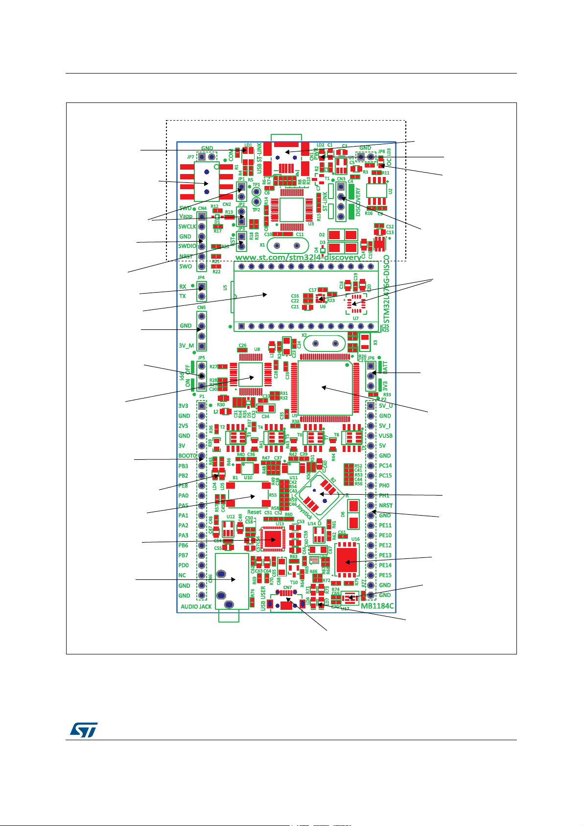
10 Hardware layout and configuration
The STM32L476 Discovery board is designed around the STM32L476VGT6 (100-pin LQFP
package). The hardware block diagram (see
the STM32L476VGT6 and the peripherals (9-axis motion sensors, digital microphone
MEMS, LCD segment, 128
Mbytes of Quad-SPI Flash memory, SAI Audio DAC stereo with
3.5mm output jack, USB OTG FS, IDD current measurement, LEDs, push-button, joystick)
and the
Figure 3 will help to locate these features on the STM32L476 Discovery board.
Figure 2. Hardware block diagram
Figure 2) illustrates the connection between
10/41 UM1879 Rev 4
Page 11
UM1879 Hardware layout and configuration
069
&1DXGLR
RXWSXWMDFN
&186%86(5
&15)((3520
&1QRWILWWHG
-3-3QRWILWWHG
-3EDWWHU\RULQWHUQDO
9UHJXODWRUVHOHFWLRQ
3H[WHQVLRQ
FRQQHFWRU
3H[WHQVLRQ
FRQQHFWRU
-3567
/'/'8VHU/('V
&167/,1.WR',6&2
ERDUGRU6:'
&16:'
-3,GG212))
8670/9*7
80(06PLFURSKRQH
&186%67/,1.
/'&20
-35;7;
8/&'VHJPHQW
80);
%5HVHWSXVKEXWWRQ
8$XGLR'$&
/'/'86%/('V
84XDG63,)ODVK
PHPRU\
%MR\VWLFN
/'3:5
/'2&
88
D[LVPRWLRQVHQVRUV
67/,1.9
Figure 3. STM32L476 Discovery board top layout
UM1879 Rev 4 11/41
40
Page 12
Hardware layout and configuration UM1879
069
&5EDWWHU\FRQQHFWRU
6%6%
N+]&/.
6%6%
27*)6
6%7B6:2
6%67/,1.3:5
6%6%6%6%
GHIDXOW
6%6%6%6%
UHVHUYHG
6%670B567
6%
UHVHUYHG
6%6%
0+]&/.
6%6%
UHVHUYHG
6%%5(6(7
6%6%
0);86$575;7;
6%(;75)(3
6%
95(*LQSXW
6%6%
86$575;7;
6%7B6:2
6%
95(*LQKLELW
Figure 4. STM32L476 Discovery board bottom layout
12/41 UM1879 Rev 4
Page 13
UM1879 Hardware layout and configuration
10.1 Embedded ST-LINK/V2-1
The ST-LINK/V2-1 programming and debugging tool is integrated on the STM32L476
Discovery board. Compared to ST-LINK/V2 the changes are listed below.
The new features supported on ST-LINK/V2-1 are:
• USB software re-enumeration
• Virtual Com Port interface on USB
• Mass storage interface on USB
• USB power management request for more than 100mA power on USB
These features are no more supported on ST-LINK/V2-1:
• SWIM interface
• Application voltage lower than 3 V
For all general information concerning debugging and programming features common
between V2 and V2-1 refer to ST-LINK/V2 in-circuit debugger/programmer for STM8 and
STM32 User manual (UM1075).
There are two different ways to use the embedded ST-LINK/V2-1 depending on the jumper
states:
• Program/debug the STM32L476VGT6 on board (Section 10.1.3)
• Program/debug an STM32 in an external application board using a cable connected to
SWD connector CN4 (Section 10.1.4)
.
Table 3. Jumper states
Jumper state Description
Both CN3 jumpers ON ST-LINK/V2-1 functions enabled for on-board programming (default)
Both CN3 jumpers OFF
10.1.1 Drivers
The ST-LINK/V2-1 requires a dedicated USB driver, which can be found on the www.st.com
website.
In case the STM32L476 Discovery board is connected to the PC before the driver is
installed, some interfaces may be declared as “Unknown” in the PC device manager. In this
case the user must install the driver files, and update the driver of the connected device
from the device manager.
ST-LINK/V2-1 functions enabled for external board through external
CN4 connector (SWD supported)
UM1879 Rev 4 13/41
40
Page 14
Hardware layout and configuration UM1879
Figure 5. Updating the list of drivers in device manager
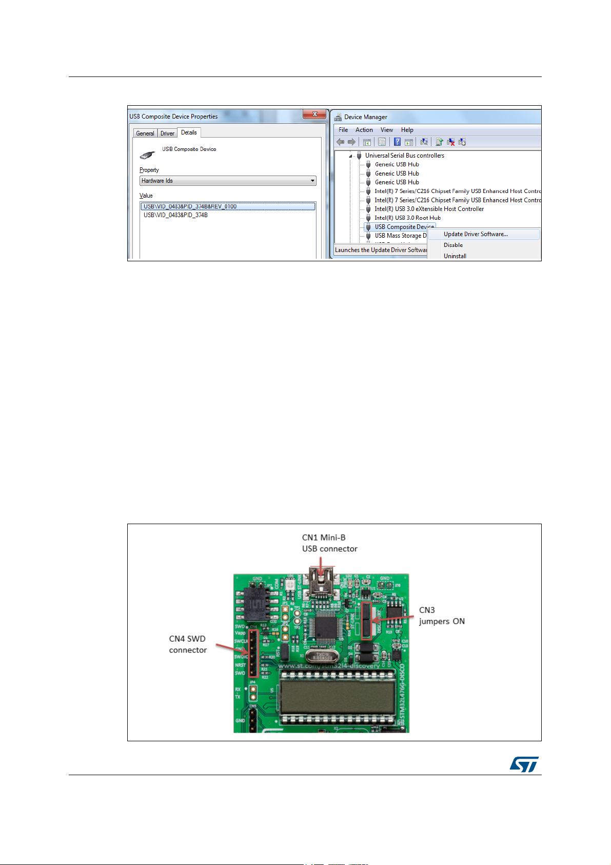
1. Prefer using the “USB Composite Device” handle for a full recovery.
10.1.2 ST-LINK/V2-1 firmware upgrade
The ST-LINK/V2-1 embeds a firmware upgrade mechanism for in-situ upgrade through the
USB port. As the firmware may evolve during the life time of the ST-LINK/V2-1 product (for
example a new functionality, bug fixes, support for new microcontroller families), it is
recommended to visit the www.st.com website before starting to use the STM32L476
Discovery board and periodically, in order to stay up-to-date with the latest firmware version.
10.1.3 Using ST-LINK/V2-1 to program/debug the STM32L476VGT6 on board
To program the STM32L476VGT6 on board, simply plug in the two jumpers on CN3, as
shown in
the Mini-B USB ST-LINK/V2-1 CN1 connector.
Make sure the jumpers JP3, JP6.3V3, and JP5.ON are set.
Do not use the CN4 connector.
Figure 6 in red, and connect the STM32L476 Discovery board to the PC through
Figure 6. CN1, CN3 (ON), CN4 connections
14/41 UM1879 Rev 4
Page 15
UM1879 Hardware layout and configuration
10.1.4 Using ST-LINK/V2-1 to program/debug an external STM32 application board
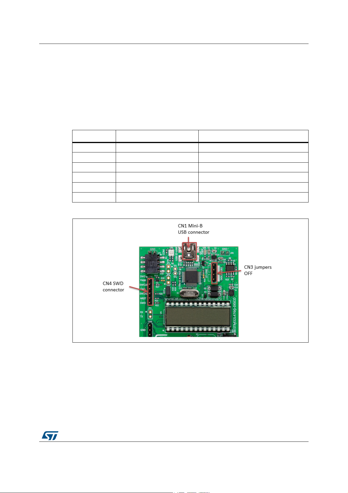
To use the ST-LINK/V2-1 to program the STM32 on an external application board (out of the
STM32L476VGT6 on board), remove the two jumpers from CN3 as shown in
red, and connect the board to the CN4 software debug connector according to Table 4.
Make sure the jumpers JP6.3V3, and JP5.OFF are set.
JP3, must be ON if CN4 pin 5 (NRST) is used in the external application board.
Pin CN4 Designation
1 Vapp VDD from application
2 SWLCK SWD clock
3 GND Ground
4 SWDIO SWD data input/output
5 NRST RESET of target MCU
6SWO Reserved
Table 4. Debug connector CN4
Figure 7 in
Figure 7. CN1, CN3 (OFF), CN4 connections
UM1879 Rev 4 15/41
40
Page 16

Hardware layout and configuration UM1879
10.2 Power supply
The power supply is provided with four options:
– ST-LINK/V2-1: CN1
– CR2032 battery (not provided): CR1
– External 5V: 5V_I
– USB FS connector: USB USER CN7
• ST-LINK/V2-1:
JP6 needs to be placed in position 3V3. JP3 is closed. JP5 is in position ON. CN3
jumpers are ON.
The STM32L476G Discovery board can be powered from the ST-LINK USB connector
CN1 (5V_USB_ST_LINK). Only the ST-LINK circuit has the power before the USB
enumeration, as the host PC only provides 100mA to the board at that time.
During the USB enumeration, the STM32L476 Discovery board requires 300 mA of
current to the host PC. If the host is able to provide the required power, the
STM32L476 is powered and the red LED LD2 is turned ON, thus the STM32L476
Discovery board and its extension board can consume no more than 300 mA current. If
the host is not able to provide the required current, the STM32L476 and the extension
board are not power supplied. As a consequence the red LED LD2 remains turned
OFF. In such case it is mandatory to use an external power supply, as explained in the
next section.
Warning: If the maximum current consumption of the STM32L476
Discovery board and its extension board exceeds 300 mA, it
is mandatory to power the STM32L476 Discovery board using
an external power supply connected to 5V_I.
Note: In case this board is powered by a USB charger or a USB battery connected on CN1, there
is no USB enumeration, the led LD2 remains OFF and the STM32L476 is not powered. In
this specific case only, fit the jumper JP2 to allow the STM32L476 to be powered anyway.
Remove this jumper JP2 if then a host PC is connected to the ST-LINK/V2-1 CN1 connector
to supply the board.
• CR2032 battery inserted in CR1 (bottom side):
– The CR2032 battery is not provided
– JP6 needs to be placed in position BATT. JP3 is opened. JP5 is in position ON
– The battery supplies the 3V3 and 3V power domains on board. All the peripherals
are powered, except the ST-LINK, which can only be supplied through the USB
connector CN1
• External 5V_I or USB USER CN7 (USB FS connector):
– External 5V_I: The pin 3 5V_I of P2 header can be used as input for an external
power supply. In this case, the STM32L476 Discovery board must be powered by
a power supply unit or by an auxiliary equipment complying with the standard EN60950-1: 2006+A11/2009, and must be Safety Extra Low Voltage (SELV) with a
limited power capability.
– To use the USB USER CN7 to power supply the board, a jumper needs to be
placed between VUSB pin 4 and the pin 3 5V_I of P2 header (see Figure 8).
16/41 UM1879 Rev 4
Page 17

UM1879 Hardware layout and configuration
Figure 8. Board jumper location
In this condition it is still possible to use the USB ST-LINK for communication, for
programming or debugging, but it is mandatory to power supply the board first using
5V_I or USB USER CN7 then connect the USB ST-LINK cable to the PC. Proceeding
this way ensures that the enumeration occurs thanks to the external power source.
The following power sequence procedure must be respected:
1. Connect the external power source to 5V_I or USB USER CN7.
2. Power on the external power supply 5V_I or USB USER CN7.
3. Check that LD2 is turned ON.
4. Connect the PC to USB ST-LINK connector CN1.
If this order is not respected, the board may be supplied by 5V_USB_ST_LINK first
then by 5V_I or USB USER CN7 and the following risks may be encountered:
1. If more than 300 mA current is needed by the board, the PC may be damaged or the
current supply can be limited by the PC. As a consequence the board is not powered
correctly.
2. 300 mA is requested at enumeration (since JP2 must be OFF) so there is risk that the
request is rejected and the enumeration does not succeed if the PC cannot provide
such current. Consequently the board is not power supplied (LED LD2 remains OFF).
Note: The headers pins 5V (except in battery mode), 3V3, 2V5, 3V can be used as output power
supply when an extension board is connected to the P1 and P2 headers. The power
consumption of the extension board must be lower than 100 mA.
UM1879 Rev 4 17/41
40
Page 18

Hardware layout and configuration UM1879
10.3 Clock source
The STM32L476VGT6 MCU uses:
• A 32.768 KHz low-speed source:
– By default, the X3 crystal on board
– From an external oscillator through P2 header (pin 7 labeled ‘PC14’). The
configuration needed is:
SB19 opened, SB20 closed, R26 removed
• A system clock source:
– By default, generated by an internal STM32L476VGT6 oscillator. The
configuration needed is:
SB18 opened, SB21 and SB22 closed
– Or driven by an X2 Crystal on board (not fitted). The configuration needed is:
SB18, SB21 and SB22 opened
X2, R88, R89, C77, C78 fitted
– Or driven by a MCO signal (8MHz) from the ST-LINK MCU STM32F103CBT6
(U3).The configuration needed is:
SB18 closed, SB22 opened
R89 not fitted
– Or driven externally from PH0 through the P2 header, pin 9 labeled ‘PH0’.The
configuration needed is:
SB22 closed, SB18 opened
R89 not fitted
Note: Refer to Oscillator design guide for STM8S, STM8A and STM32 microcontrollers
Application note (AN2867).
10.4 Reset source
The reset signal NRST of the STM32L476 Discovery board is low active and the reset
sources include:
• The reset button B1, connected by default to NRST (SB23 closed)
• The embedded ST-LINK/V2-1
• The external reset pin 11 of P2 header connector, labeled ‘NRST’
• The external reset from SWD connector CN4, pin 5
Jumper Description
JP3
Table 5. Reset related jumper
When JP3 is closed, the SWD connector CN4 pin 5 and the embedded
ST-LINK/V2-1 are connected to NRST.
Default Setting: closed
JP3 is opened, no connection between CN4 and ST-LINK/V2-1 to
NRST. This must be used when the ST-LINK/V2-1 is not powered (i.e
STM32L476 Discovery board) is powered by the CR2032 battery
18/41 UM1879 Rev 4
Page 19

UM1879 Hardware layout and configuration
10.5 User interface: LCD, joystick, LEDs
The STM32L476 Discovery board features sept LEDs with the following functionalities:
• LD1 COM: LD1 default status is red. LD1 turns to green to indicate that
communications are in progress between the PC and the ST-LINK/V2-1
• LD2 PWR: the red LED indicates that the board is powered
• LD3 OC: the red LED indicates a fault when the board is in current limit (510 mA)
• LD4 user: the red LED is a user LED connected to the I/O PB2 of the
STM32L476VGT6
• LD5 user: the green LED is a user LED connected to the I/O PE8 of the
STM32L476VGT6
• LD6, LD7: USB OTG FS LEDs, see Section 10.8
Four-direction joystick (B2) with selection and a reset push-button (B1) are available as
input devices.
An LCD 4x24 segments, 4 commons, multiplexed 1/4 duty, 1/3 bias is mounted on the
DIP28 connector U5.
10.6 Boot0 configuration
Boot0 is by default grounded through a pull-down R91.
It is possible to set Boot0 high, removing R91 and putting a jumper between P1 header
pin 6 BOOT0 and pin 5 3V.
10.7 Quad-SPI NOR Flash memory
128-Mbit Quad-SPI NOR Flash memory is connected to Quad-SPI interface of
STM32L476VGT6.
10.8 USB OTG FS
The STM32L476 Discovery board supports USB OTG Full Speed communication via a USB
Micro-AB connector (CN7) and a USB power switch (U14) connected to VBUS. The board
can be powered by this USB connection as described in
A green LED LD6 will be lit in one of these cases:
• The power switch (U14) is ON and STM32L476 Discovery board works as a USB host
• VBUS is powered by another USB host when STM32L476 Discovery board works as a
USB device
Red LED LD7 will be lit when an overcurrent occurs.
In order to connect the OTG_FS_VBUS and OTG_FS_ID signals from the connector CN7 to
the OTG FS hardware IP of STM32L476VGT6, remove the LCD from its socket U5, and
close SB24 and SB25.
Section 10.2.
The default configuration is: the LCD is connected to U5, and SB24 and SB25 are opened.
In this case the OTG_FS_VBUS and OTG_FS_ID signals from CN7 are connected to the
OTG FS peripheral of the STM32L476VGT6 available on PC11 and PC12.
UM1879 Rev 4 19/41
40
Page 20

Hardware layout and configuration UM1879
069
10.9 USART configuration
The USART interface available on PD5 and PD6 of the STM32L476VGT6 can be
connected to the ST-LINK MCU to use the Virtual Com Port function.
To use the Virtual Com Port function with:
• The on-board STM32L476VGT6: set SB13 and SB16 ON (SB15, SB17 must be OFF).
• An external MCU: remove solder from SB13 and SB16, solder a two pins header on
JP4, then RX and TX of the external MCU can be connected directly to RX and TX of
JP4.
(For more details see Section 11 : S c h e m a ti c s )
10.10 Audio DAC and MEMS microphone
An audio stereo DAC CS43L22 (U13) is connected to SAI interface of STM32L476VGT6.
The STM32L476VGT6 controls the audio DAC via the I2C1 bus which is shared with the I2C
extension connector CN2.
I2C1 is also available on the connector P1, pins labeled ‘PB6’ (I2C1_SCL) and ‘PB7’
(I2C1_SDA).
The stereo output jack connector is CN6.
Note: I2C address of CS43L22 is 0x94.
A MEMS audio sensor omnidirectional digital microphone provides a digital signal in PDM
format to the STM32L476VGT6.
10.11 9-axis motion sensors
STM32L476 Discovery board supports some 9-axis motion sensors, composed of:
• L3GD20 (U7): a three-axis digital output gyroscope
• LSM303C (U6): a 3D accelerometer and 3D magnetometer module
which are connected to STM32L476VGT6 through SPI.
10.12 I2C extension connector CN2
Figure 9. Connector CN2
20/41 UM1879 Rev 4
Page 21

UM1879 Hardware layout and configuration
Pin number Description Pin number Description
1 I2C1_SDA (PB7) 5 +3V3
2NC6NC
3 I2C1_SCL (PB6) 7 GND
4 EXT_RST(PD0) 8 NC
10.13 MCU current ammeter
The jumper JP5, labeled Idd, allows the consumption of STM32L476VGT6 to be measured
directly by a built-in current ammeter circuit able to measure from 60nA to 50mA or by
removing the jumper and connecting an ammeter:
• Jumper on position OFF: STM32L476VGT6 is powered (default).
Table 6. Connector CN2
• Jumper on position ON: an on-board module is designed to measure from 60nA to
50mA by using several MOSFETs and switching automatically depending on the read
value.
• No jumper on JP5: an ammeter must be connected to measure the STM32L476VGT6
current through pin 1 and 2 (if there is no ammeter, the STM32L476VGT6 is not
powered).
UM1879 Rev 4 21/41
40
Page 22

Hardware layout and configuration UM1879
10.14 Extension connector P1 and P2
The P1 and P2 headers can connect the STM32L476 Discovery board to a standard
prototyping/wrapping board. STM32L476VGT6 GPIOs are available on these connectors.
P1 and P2 can also be probed by an oscilloscope, logical analyzer or voltmeter.
P1 P2
Pin number function Pin number function
Table 7. Extension connector
13V3 1
2 GND 2 GND
32V5 3
4GND 4
53V 5 5V
6BOOT0 6 GND
7 PB3 7 PC14
8 PB2 8 PC15
9 PE8 9 PH0
10 PA0 10 PH1
11 PA5 11 NRST
12 PA1 12 GND
13 PA2 13 PE11
14 PA3 14 PE10
15 PB6 15 PE12
16 PB7 16 PE13
(USB OTG FS VBUS)
5V_U
(5V_USB_ST_LINK)
5V_I
(5V INPUT)
VUSB
17 PD0 17 PE14
18 NC 18 PE15
19 GND 19 GND
20 GND 20 GND
22/41 UM1879 Rev 4
Page 23

UM1879 Hardware layout and configuration
10.15 Solder bridges
Table 8 describes each solder bridge. The default state is indicated in bold.
Bridge State Description
Table 8. Solder bridges
SB1 (ST-LINK PWR)
SB2 (EXT/RF E2P)
SB3, SB4, SB7, SB8
(RESERVED)
SB5, SB6, SB9, SB10 (DEFAULT) ON Reserved, do not modify
SB11 (STM_RST)
SB12 OFF Reserved
SB16, SB13 (USART RX, TX)
SB17, SB15 (MFX USART RX,TX)
SB14 (T_SWO)
SB18 (MCO)
ON ST-LINK module is powered
OFF ST-LINK module is not powered
ON 5V connected to CN2.8
OFF 5V is not connected to CN2.8
OFF Reserved, do not modify
ON No incidence on NRST signal of STM32F103CBT6
OFF
OFF
OFF
OFF
OFF MCO is not connected to PH0
NRST signal of STM32F103CBT6 is connected to
GND
PA2, PA3 of STM32F103CBT6 are connected to PD6,
ON
PD5 of STM32L476VGT6
PA2, PA3 of STM32F103CBT6 are not connected to
PD6, PD5 of
PA2, PA3 of STM32L476VGT6 are connected to MFX
ON
USART RX,TX
PA2, PA3 of STM32L476VGT6 are not connected to
MFX USART RX,TX
PA10 of STM32F103CBT6 is connected to PB3 of
ON
STM32L476VGT6
PA10 of STM32F103CBT6 is not connected to PB3 of
STM32L476VGT6
ON If SB22 is also ON, MCO is connected to PH0
STM32L476VGT6
SB19, SB20 (32.768kHz CLK)
SB21, SB22 (8MHz CLK)
SB23 (B1-RESET)
ON PC14, PC15 are connected to X3 crystal
OFF PC14, PC15 are not connected to X3 crystal
ON PH0, PH1 are connected to X2 crystal (X2 is not fitted)
OFF PH0, PH1 are not connected to X2 crystal
B1 push-button is connected to NRST of STM32L476
ON
Discovery board
OFF
UM1879 Rev 4 23/41
B1 push-button is not connected to NRST of
STM32L476 Discovery board
40
Page 24

Hardware layout and configuration UM1879
Table 8. Solder bridges (continued)
Bridge State Description
OTG_FS_VBUS signal is connected to PA9
ON
SB24, SB25 (OTG FS)
OFF
SB26 ON Reserved, do not modify
SB27 OFF Reserved, do not modify
SB28 (2.5V REG inhibit)
OFF U12 input is not inhibited
OTG_FS_ID signal is connected to PA10
OTG_FS_VBUS signal is not connected to PA9
OTG_FS_ID signal is not connected to PA10
ON U12 (2.5V regulator) input is inhibited
SB29 (2.5V REG input)
ON 5V is connected to U12 input
OFF 5V is not connected to U12 input
24/41 UM1879 Rev 4
Page 25

110
STM32L476 Discovery
MB1184 C-01
6/15/2015
Title:
Size: Referenc e:
Date: Sheet: of
A4
Revision:
STM32L476G-DISCOProject:
SWDIO
SWCLK
MCO
NRST
NRST
MCO
LD_R
SWCLK
SWDIO
USART_TX
USART_RX
LD_G
MFX_IRQ_OUT
MFX_WAKEUP
QSPI_D0
QSPI_D3
QSPI_D2
QSPI_D1
QSPI_CLK
QSPI_CS
SAI1_FS
SAI1_SD
SAI1_SCK
I2C1_SCL
I2C1_SDA
AUDIO_RST
SAI1_MCK
AUDIO_DIN
AUDIO_CLK
OTG_FS_PowerSwitchOn
OTG_FS_DM
OTG_FS_DP
OTG_FS_ID
OTG_FS_VBUS
OTG_FS_OverCu rrent
SEG[0..23]
COM[0..3]
EXT_RST
PH[0..1]
JOY_CENTER
JOY_DOWN
JOY_LEFT
JOY_RIGHT
JOY_UP
MEMS_SCK
MEMS_MISO
MEMS_MOSI
GYRO_CS
GYRO_INT1
GYRO_INT2
XL_CS
XL_INT
MAG_CS
MAG_DRDY
MAG_INT
MFX_USART3_RX
MFX_USART3_TX
MFX_I2C_SDA
MFX_I2C_SCL
BOOT0
SWO
3V3_REG-ON
PC14
PC15
U_STM32Lx
STM32Lx.SchDoc
Rev A-01 --> PCB label MB1184 A-0 1
Rev B-01 --> PCB label MB1184 B-01, Remove R91, Replace COM4..7 by COM0..3,
Add SB for USB_OTG, add VBUS on P2 for USB USE R power supply
Rev C-01 --> PCB label MB1184 C-01, Remove
SWCLK and SWO shorted,
Replaced on P1, PB8..9 by PB6..7.
--> MP45DT02 replaced by MP34DT01
--> Xta l 32.768kHz replaced by NX3215SA
--> Change values of C27, C25 : C27=C25=4.7pF
USART_TX
USART_RX
3V
GND
GND
NRST
PC14
PC15
PH1
PH0
BOOT0
5V_IN
5V
SWDIO
SWCLK
MCO
NRST
USART_RX
USART_TX
MFX_USART3_RX
MFX_USART3_TX
SWO
3V3_REG-ON
U_ST_LINK_V2-1
ST_LINK_V2-1.SCHDOC
MFX_WAKEUP
MFX_IRQ_OUT
MFX_I2C_SDA
MFX_I2C_SCL
MFX_USART3_RX
MFX_USART3_TX
NRST
U_IDD_measurement
IDD_measurement.SchDoc
MFX_I2C_SCL
MFX_I2C_SDA
MFX_IRQ_OUT
MFX_WAKEUP
MFX_USART3_RX
MFX_USART3_TX
MFX_USART3_RX
MFX_USART3_TX
3V3
AUDIO_CLK
AUDIO_DIN
AUDIO_RST
SAI1_FS
SAI1_SD
SAI1_SCK
I2C1_SCL
I2C1_SDA
SAI1_MCK
U_AUDIO
AUDIO.SchDoc
OTG_FS_PowerSwitchOn
OTG_FS_OverCu rrent
OTG_FS_DM
OTG_FS_DP
OTG_FS_ID
OTG_FS_VBUS
U_USB_OTG_FS
USB_OTG_FS.SchDoc
NRST
LD_R
LD_G
EXT_RST
JOY_CENTER
JOY_DOWN
JOY_LEFT
JOY_RIGHT
JOY_UP
I2C1_SCL
I2C1_SDA
U_Peripherals
Peripherals.SchDoc
SEG[0..23]
COM[0..3]
U_LCD_GH08172
LCD_GH08172.SchDoc
I2C1_SCL
I2C1_SDA
SAI1_MCK
SAI1_SCK
SAI1_SD
SAI1_FS
AUDIO_RST
AUDIO_DIN
AUDIO_CLK
SEG[0..23]
COM[0..3]
OTG_FS_PowerSwitchOn
OTG_FS_OverCu rrent
OTG_FS_DM
OTG_FS_DP
OTG_FS_ID
OTG_FS_VBUS
NRST
LD_R
LD_G
EXT_RST
JOY_CENTER
JOY_DOWN
JOY_LEFT
JOY_RIGHT
JOY_UP
I2C1_SCL
I2C1_SDA
PH[0..1]
QSPI_D0
QSPI_D3
QSPI_D2
QSPI_D1
QSPI_CLK
QSPI_CS
U_QSPI
QSPI.SchDoc
QSPI_D0
QSPI_D1
QSPI_D2
QSPI_D3
QSPI_CS
QSPI_CLK
GYRO_CS
MAG_CS
MAG_INT
XL_INT
MAG_DRDY
MEMS_SCK
MEMS_MISO
MEMS_MOSI
GYRO_INT1
GYRO_INT2
XL_CS
U_MEMS
MEMS.SchDoc
GYRO_INT1
GYRO_INT2
MEMS_SCK
GYRO_CS
MEMS_MISO
MEMS_MOSI
MAG_CS
XL_CS
MAG_DRDY
XL_INT
MAG_INT
NRST
SEG[0..23]
COM[0..3]
LD_R
LD_GEXT_RST
JOY_CENTER
JOY_DOWN
JOY_LEFT
JOY_RIGHT
JOY_UP
I2C1_SCL
I2C1_SDA
GYRO_INT1
GYRO_INT2
MEMS_SCK
GYRO_CS
MEMS_MISO
MEMS_MOSI
MAG_CS
XL_CS
MAG_DRDY
XL_INT
MAG_INT
OTG_FS_PowerSwitchOn
OTG_FS_OverCu rrent
OTG_FS_DM
OTG_FS_DP
OTG_FS_ID
OTG_FS_VBUS
SWDIO
SWCLK
MCO
NRST
QSPI_D0
QSPI_D1
QSPI_D2
QSPI_D3
QSPI_CS
QSPI_CLK
SAI1_MCK
SAI1_SCK
SAI1_SD
SAI1_FS
AUDIO_RST
AUDIO_DIN
AUDIO_CLK
USART_TX
USART_RX
BOOT0
MFX_I2C_SCL
MFX_I2C_SDA
MFX_IRQ_OUT
MFX_WAKEUP
MFX_USART3_RX
MFX_USART3_TX
3V3_REG-ON
SWO
SWO
3V3_REG-ON
2V5
GND
GND
Wired on Solder Side
JP8
JP7
5V_USB_ST_LINK
GND
GND
GND
GND
GND
NC
3V3_REG-ON
QSPI_CLK
QSPI_CS
QSPI_D0
QSPI_D1
QSPI_D2
QSPI_D3
JOY_CENTER
JOY_LEFT
JOY_RIGHT
JOY_UP
JOY_DOWN
LD_R
LD_G
EXT_RST
I2C1_SCL
I2C1_SDA
1
2
3
4
5
6
7
8
9
10
11
12
13
14
15
16
17
18
19
20
P1
Header 20
1
2
3
4
5
6
7
8
9
10
11
12
13
14
15
16
17
18
19
20
P2
Header 20
PB2
PE8
PA0
PA5
PA1
PA2
PA3
PB6
PB7
PD0
PE11
PB3
PE10
PE12
PE13
PE14
PE15
OTG_FS_VBUS
PC14
PC15
11 Schematics
UM1879 Rev 4 25/41
Figure 10. STM32L476 Discovery board design top sheet
--> Change values of resistors : R40=R47=6.04k, R49=15k,
UM1879 Schematics
Page 26

26/41 UM1879 Rev 4
210
ST-LINK/V2-1 with support of SWD only
MB1184 C-01
6/15/2015
Title:
Size: Reference:
Date: Sheet: o f
A4
Revision:
STM32L476G-DISCOProject:
USB_DM
USB_DP
STM_RST
T_JTCK
T_JTCK
T_JTMS
STM_JTMS
STM_JTCK
OSC_IN
OSC_OUT
T_NRST
AIN_1
3V3_ST_LINK
3V3_ST_LINK
SWIM_IN
USB_DM
USB_DP
USB
VCC
1
D-
2
D+
3
ID
4
GND
5
SHELL
6
CN1
USB-MINI-typeB
COM
ST-LINK Power
3V3_ST_LINK
Jumpers ON --> DISCOVERY Selected
Jumpers OFF --> ST-LINK Selected
Board Ident: PC13=0
T_JTCK
T_JTMS
SWD
3V3_ST_LINK
123
4
CN3
SB5 SB3
SB6 SB4
SB9 SB7
SB10 SB8
STM_JTMS
STM_JTCK
SWCLK
SWDIO
SWD
RESERVED
DEFAULT
3V3_ST_LINK
T_SWDIO_IN
T_SWO
LED_STLINK
LED_STLINK
3V3_ST_LINK
Red
_Green
2 1
3 4
LD1
LD_BICOLOR_CMS
SWDIO
SWCLK
TCK/SWCLK
TMS/SWDIO
Not Fitted
MCO
MCO
T_JRST
1
2
3
4
5
6
CN4
5075BMR-05-SM
AIN_1
T_NRST
T_SWO
NRST
T_NRST
SB11
RC Must be very close to STM32F103 pin 29
51
2
GND
3
4
BYPASS
INH
Vin Vout
U1 LD3985M33R
D1
BAT60JFILM
TX
RX
SB16
SB13
USART_RX
USART_TX
Close to JP
Not Fitted
STLINK_TX
STLINK_RX
Not Fitted
LD2
LED, red
C7
100nF
C71
100nFC6100nFC8100nF
C5
1uF
C1
1uF
C2
100nF
C4
100nF
C3
10nF
C10
20pF
C11
20pF
C73
100nF
C72
20pF
1 2
X1
8MHz
3V3_ST_LINK
USB_RENUMn
PWR_EXT
PWR_ENn
3V3_ST_LINK
3
1
2
T1
9013-SOT23
3V3_ST_LINK
USB_RENUMn
PA14
PA13
PWR_ENn
TP2
TP1
EN
1
GND
2
VO
4
NC
5
GND
7
VI
6
PG
3
U4 LD39050PU33R
C14
1uF
C15
100nF
C13
1uF
C12
100nF
3V3_ST_LINK
5 Volts Output
3 Volts Output
5 Volts From External
5V_IN
5V_IN
5 Volts From USB ST-LINK
JP4
3V3_ST_LINK
3V3_ST_LINK
VBAT
1
PA7
17
PC13
2
PA12
33
PC14
3
PB0
18
PC15
4
JTMS/SWDIO
34
OSCIN
5
PB1
19
OSCOUT
6
VSS_2
35
NRST
7
PB2/BOOT1
20
VSSA
8
VDD_2
36
VDDA
9
PB10
21
PA0
10
JTCK/SWCLK
37
PA1
11
PB11
22
PA2
12
PA15/JTDI
38
PA3
13
VSS_1
23
PA4
14
PB3/JTDO
39
PA5
15
VDD_1
24
PA6
16
PB4/JNTRST
40
PB12
25
PB5
41
PB13
26
PB6
42
PB14
27
PB7
43
PB15
28
BOOT0
44
PA8
29
PB8
45
PA9
30
PB9
46
PA10
31
VSS_3
47
PA11
32
VDD_3
48
U3
STM32F103CBT6
5V
D3
STPS1L30A
D2
STPS1L30A
JP1
5V_USB_ST_LINK
5V_USB_ST_LINK
MFX_USART3_RX
MFX_USART3_TX
SB17
SB15
D4
BAT60JFILM
Not Fitted
12
CR1
CR2032 Holder
IN
1
IN
2
ON
3
GND
4
SET
5
OUT
6
OUT
7
FAULT
8
U2
ST890CDR
51
2
GND
3
4
BYPASS
INH
Vin Vout
U12 LD3985M25R
C47
1uF
C48
100nF
C49
10nF
C54
100nF
C55
1uF
2V55V
R11
10K_1%_0402
C9
100nF
123
JP6
D6
STPS1L30A
3V
3V3_REG
R18
4K7_1%_0402
R82
10K_1%_0402
R83
[NA]
R14
100K_1%_0402
R86
100K_1%_0402
R85
4K7_1%_0402
R84
4K7_1%_0402
R1
0_5%_0402
R79
100_1%_0402
R10
10K_1%_0402
R8
0_5%_0402
R9 0_5%_0402
R7
1K5_1%_0402
5V_USB_ST_LINK
R78
36K_1%_0402
R2
1K_1%_0402
R19
2K7_1%_0402
R80
100_1%_0402
R81
100_1%_0402
R17
22_1%_0402
R20
22_1%_0402
R21
22_1%_0402
R22
22_1%_0402
R13
[NA]
R12
10K_1%_0402
JP2
SWO
SB14
T_SWO
PB3
R33
4K7_1%_0402
3V3
3V3
3V3_REG
R4
330_1%_0402
R5
330_1%_0402
3V3_REG-ON
3V3_REG-ON
JP3
R15
[NA]
2.5 Volts Output
SB1
SB29
SB28
T_JTDI
T_JTDO
SWIM
SWIM_RST
SWIM_RST_IN
R6 100K_1%_0402
3V3_REG
SB12
R16
2K7_1%_0402
Ilim = 510mA
Isc= 1.2Ilim to 1.5Ilim = 612mA to 765mA
LD3
LED, red
R3
1K_1%_0402
Figure 11. ST-LINK/V2-1 with support of SWD only
Schematics UM1879
Page 27
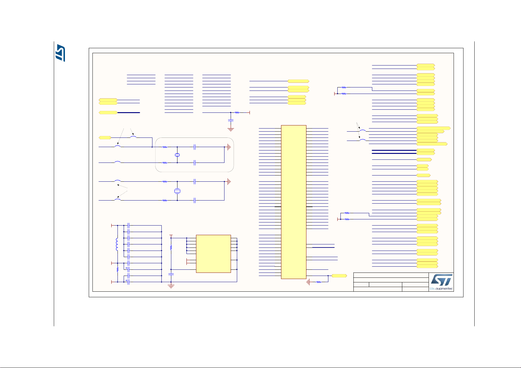
Figure 12. STM32L476VGT6 MCU
310
STM32L476VGT6 MCU
MB1184 C-01
6/15/2015
Title:
Size: Reference:
Date: Sheet: of
A4
Revision:
STM32L476G-DISCOProject:
PA0
Must be close to the MCU
All this block must be very close to the STM32L476
SWCLK
SWDIO
SWDIO
SWCLKPA14
PA13
USART_TX
USART_RX
PD5
USART_TX
USART_RX
PC14-OSC32_IN
PC15-OSC32_OUT
SB19
SB20
Must be close to the Crystal
PE2
1
PE3
2
PE4
3
PE5
4
PE6
5
PC13
7
PC14
8
PC15
9
PH0
12
PH1
13
NRST
14
PC0
15
PC1
16
PC2
17
PC3/VLCD
18
PA0
23
PA1
24
PA2
25
PA3
26
PA4
29
PA5
30
PA6
31
PA7
32
PC4
33
PC5
34
PB0
35
PB1
36
PB2
37
PE7
38
PE8
39
PE9
40
PE10
41
PE11
42
PE12
43
PE13
44
PE14
45
PE15
46
PB10
47
PB11
48
PB12
51
PB13
52
PB14
53
PB15
54
PD8
55
PD9
56
PD10
57
PD11
58
PD12
59
PD13
60
PD14
61
PD15
62
PC6
63
PC7
64
PC8
65
PC9
66
PA8
67
PA9
68
PA10
69
PA11
70
PA12
71
PA13
72
PA14
76
PA15
77
PC10
78
PC11
79
PC12
80
PD0
81
PD1
82
PD2
83
PD3
84
PD4
85
PD5
86
PD6
87
PD7
88
PB3
89
PB4
90
PB5
91
PB6
92
PB7
93
BOOT0
94
PB8
95
PB9
96
PE0
97
PE1
98
U9A
STM32L476VGT6
VBAT
6
VSS4
27
VSS2
74
VREF-
20
VREF+
21
VDDA_ADC
22
VSS5
10
VDDUSB
73
VDD3
100
VSS1
49
VDD2
75
VDD1
50
VDD4
28
VSSA_ADC
19
VDD5
11
VSS3
99
U9B
STM32L476VGT6
PA1
PA2
PA3
PA4
PA5
PA6
PA7
PA8
PA9
PA10
PA11
PA12
PA13
PA14
PA15
PB0
PB1
PB2
PB3
PB4
PB5
PB6
PB7
PB8
PB9
PB10
PB11
PB12
PB13
PB14
PB15
PC0
PC1
PC2
PC3
PC4
PC5
PC6
PC7
PC8
PC9
PC10
PC11
PC12
PC13
PD0
PD1
PD2
PD3
PD4
PD5
PD6
PD7
PD8
PD9
PD10
PD11
PD12
PD13
PD14
PD15
PE0
PE1
PE2
PE3
PE4
PE5
PE6
PE7
PE8
PE9
PE10
PE11
PE12
PE13
PE14
PE15
NRST
BOOT0
PC14
PH[0..1]
MCO
PH1-OSC_OUT
SB21
SB22
MCO
1 2
X2
8MHz
SB18
PH0-OSC_INPH0
PH1
QSPI_D0
QSPI_D3
QSPI_D2
QSPI_D1
QSPI_CLK
QSPI_CS
QSPI_D0
QSPI_D1
QSPI_D2
QSPI_D3
QSPI_CS
QSPI_CLK
SAI1_FS
SAI1_SD
SAI1_SCK
I2C1_SCL
I2C1_SDA
AUDIO_RST
SAI1_MCK
AUDIO_DIN
AUDIO_CLK
OTG_FS_PowerSwitchOn
OTG_FS_DM
OTG_FS_DP
OTG_FS_ID
OTG_FS_VBUS
OTG_FS_OverC urrent
SEG[0..23]
COM[0..3]
SEG[0..23]
COM[0..3]
EXT_RST
EXT_RST
LD_R
LD_G
LD_R
LD_G
NRST
NRST
JOY_CENTER
JOY_DOWN
JOY_LEFT
JOY_RIGHT
JOY_UP
JOY_CENTER
JOY_DOWN
JOY_LEFT
JOY_RIGHT
JOY_UP
MFX_USART3_RX
MFX_USART3_TX
MFX_USART3_RX
MFX_USART3_TX
MFX_WAKEUP
MFX_WAKEUP
MFX_IRQ_OUT
MFX_IRQ_OUT
MFX_I2C_SDA
MFX_I2C_SCL
MFX_I2C_SCL
MFX_I2C_SDA
PE10
PE11
PE12
PE13
PE14
PE15
PB6
PE2
PE3
PE4
PE5
PE6
PE7
PE9
PA0
PA1
PA2
PA3
PA4
PA5
PC13
PB10
PB11
PB2
PE8
PD0
PA11
PA12
PC9
SAI1_MCK
AUDIO_RST
SAI1_FS
SAI1_SCK
SAI1_SD
COM0
COM1
COM2
COM3
SEG0
SEG1
SEG2
SEG3
SEG4
SEG5
SEG6
SEG7
SEG8
SEG9
SEG10
SEG11
SEG12
SEG13
SEG14
SEG15
SEG16
SEG17
SEG18
SEG19
SEG20
SEG21
SEG22
SEG23
GYRO_CS
GYRO_INT1
GYRO_INT2
MEMS_SCK
GYRO_CS
MEMS_MISO
MEMS_MOSI
MEMS_SCK
MEMS_MISO
MEMS_MOSI
GYRO_INT1
GYRO_INT2
MAG_CS
MAG_CS
XL_CS
XL_CS
XL_INT
MAG_DRDY
MAG_DRDY
XL_INT
MAG_INT
MAG_INT
PE0
PE1
PC0
PC1
PC2
PD1
PD3
PD4
PD7
PD6
PA6
PA7
PA15
PB0
PB1
PB4
PB5
PB12
PB13
PB14
PB15
PC3
PC4
PC5 PC6
PC7
PC8
PD8PD9
PD10
PD11
PD12
PD13
PD14
PD15
VLCD
AUDIO_DIN
AUDIO_CLK
I2C1_SCL
I2C1_SDA
OTG_FS_OverCurrent
OTG_FS_VBUS
OTG_FS_ID
OTG_FS_DM
OTG_FS_DP
OTG_FS_PowerSwitchOn
VDD_MCU
C76
1uF_X5R_10%_0603
R91
510_1%_0402
L1
Ferrite
C35
100nF_X7R_10%_0402
C74
1uF_POL_10%_TANA
C23
1uF_POL_10%_TANA
C79
1uF_X5R_10%_0603
C82
100nF_X7R_10%_0402
C81
100nF_X7R_10%_0402
C75
100nF_X7R_10%_0402
C29
100nF_X7R_10%_0402
C80
100nF_X7R_10%_0402
VDDA VDDA
R24
47_1%_0402
C24
100nF_X7R_10%_0402
VREF+
VREF+
VDD_MCU
C83
100nF_X7R_10%_0402
R90
0_5%_0402
VDD_MCU
3V
C78
20pF_NPO_5%_0402
C77
20pF_NPO_5%_0402
R89
0_5%_0402
R26
0_5%_0402
R25
0_5%_0402
R88
220_1%_0402
PC14
PH[0..1]
R31
4K7_1%_0402
R32
4K7_1%_0402
3V
R92
2K2_1%_0402
R93
2K2_1%_0402
PC14
PC15
PH1-OSC_OUT
PH0-OSC_IN
PC14-OSC32_IN
PC15-OSC32_OUT
BOOT0
SWO
3V3_REG-ON
3V3_REG-ON
SWOPB3
PB3
Not Fitted
PA8
PA9
PA10
PB9
PD2
PB7
PB8
PC10
PC11
PC12
PA9
PA10
SB24
SB25
Layout priority to PA9, PA10
R87
[NA]
X3
NX3215SA-32.768K
PC15
PC15
C27
4.7pF_NPO_-+0.25pF_0402
C25
4.7pF_NPO_-+0.25pF_0402
UM1879 Schematics
UM1879 Rev 4 27/41
Page 28

28/41 UM1879 Rev 4
410
IDD measurement / MFX (Multi Function eXpander)
MB1184 C-01
6/15/2015
Title:
Size: R eference:
Date: She et: of
A4
Revision:
STM32L476G-DISCOProject:
VDD_MCU
3V_MFX
Current
direction
to MCU
differential
amplifier
CAL
SH0 SH1 SH2
Shunts
3
4
5
G
SD
6
2
1
T3
STT7P2UH7
3
4
5
G
SD
6
2
1
T7
STT7P2UH7
3
4
5
G
SD
6
2
1
T9
STT7P2UH7
3
4
5
G
SD
621
T5
STT7P2UH7
3V3
decoupling capacitors
close to TSZ122
MFX_IRQ_OUT
IDD_MEAS
MFX_SWCLK
CAL
SH2
SH1
MFX_SWDIO
IDD_MEAS
see note *
SH1_D SH2_DSH0_D
CAL_D
435
G
SD
6
7
8
2
1T2
STS9P2UH7
3V_MFX
SH0_D
SH0
435
G
SD
6
7
8
2
1T4
STS9P2UH7
3V_MFX
CAL_D
CAL
435
G
SD
6
7
8
2
1T6
STS9P2UH7
SH1_D
SH1
435
G
SD
6
7
8
2
1T8
STS9P2UH7
SH2_D
SH2
CAL_D
CAL_D
3V
3V_MFX
one capacitor close to each MFX pins:
SH0
VDD_MCU
MFX_WAKEUP
L2
Ferrite
MFX_I2C_SDA
MFX_I2C_SCL
123
JP5
bypass
R36
100K_1%_0402
R37
100K_1%_0402
R39
1_1%_0805
R43
24_1%_0805
R44
620_1%_0805
R41
10K_1%_0805
R34
100K_1%_0402
R29
10K_1%_0402
C33
100nF_X7R_10%_0402
C341uF_POL_10%_TANA
C26
100nF_X7R_10%_0402
R38
100K_1%_0402
R94
100K_1%_0402
MFX_USART3_RX
MFX_USART3_TX
MFX_USART3_RX
MFX_USART3_TX
3V_MFX
1
2
3
4
CN5
MFX_SWCLK
MFX_SWDIO
C30
100nF_X7R_10%_0402
C31
100nF_X7R_10%_0402
C28
100nF_X7R_10%_0402
C37
100nF_X7R_10%_0402
C40
1uF_X5R_10%_0603
R51
100_1%_0402
C39
100nF_X7R_10%_0402
V+
V-
3
2
1
4 8
U11A
TSZ122IST
5
6
7
U11B
TSZ122IST
V+
V-
3
2
1
4 8
U10A
TSZ122IST
5
6
7
U10B
TSZ122IST
C36
100nF_X7R_10%_0402
see note *
see note *
see note *
Note *: two footprints superimposed allows to
also populate with SO-8 package.
(STS9P2UH7 P MOS transistors)
LAYOUT PROPOSAL DRAWING
C38
100nF_X7R_10%_0402
3V3
decoupling capacitors
close to TSZ122
R27
0_5%_0402
MFX_I2C_SCL
MFX_I2C_SDA
MFX_WAKEUP
MFX_IRQ_OUT
R28
510_1%_0402
R35
[NA]
NRST
C32
[NA]
NRST
MFX_I2C_SCL
MFX_I2C_SDA
R30
0_5%_0603
3V_MFX
3V_MFX
3V_MFX
3V_MFX
PC13
PB10
PA4
PB11
SB27
SB26
D5 BAT60JFILM
VDD
1
WAKEUP
2
IDD_CAL/GPO4
3
IDD_SH0
4
IDD_SH1/GPO5
5
IDD_SH2/GPO6
6
NRST
7
VSSA
8
VDDA
9
TSC_XP/GPO0
10
TSC_XN/GPO1
11
TSC_YP/GPO2
12
TSC_YN/GPO3
13
IDD_MEAS
14
GPIO0
18
GPIO1
19
GPIO2
20
GPIO3
39
GPIO4
40
GPIO5
15
USART_TX
21
USART_RX
22
VSS_1
23
VDD_1
24
SPARE
25
GPIO6
16
GPIO7
17
GPIO8
29
GPIO9
30
GPIO10
31
GPIO11
32
GPIO12
33
GPIO13
26
SWDIO
34
VSS_2
35
VDD_2
36
SWCLK
37
IDD_SH3/GPO7
38
GPIO14
27
GPIO15
28
IDD_VDD_MCU
41
I2C_SCL
42
I2C_SDA
43
BOOT0
44
I2C_ADDR
45
IRQOUT
46
VSS_3
47
VDD_3
48
W
A
KEUP
_
G
O
IDD
S
H
0
IDD_SH
GPO
5
IDD_SH
2/GPO
6
N
S
T
TS
C
_
P/GP
O
0
TS
C
_X
N
/GPO
1
TS
C
Y
/G
O
TS
C
_Y
N
/G
O
3
IDD
A
S
G
P
I
O
0
GPO
G
P
IO2
G
I
O
3
G
IO4
GPO
5
U
S
A
R
T_TX
U
S
T_R
P
I
P
I
P
I
P
I
P
IWD
I
W
G
P
I
P
I
IDD_VD
D
_MC
U
I
2C
_S
L
I
2C
S
D
A
B
0
I
2C
A
DDR
U
MFX_V2
U8
MFX_V2
R47
6K04_1%_0402
R40
6K04_1%_0402
R49
15K_1%_0402
R42
300K_1%_0402
R50
300K_1%_0402
R48
300K_1%_0402
Figure 13. IDD measurement / MFX (Multi Function eXpander)
Schematics UM1879
X
_
T
O
R
_
_
P
P
1
_
1/
D_SH3/
C
L/
_ME
VDD, VDD 1, VDD 2, VDD 3
Page 29

Figure 14. Joystick ACP, LEDs and push-button
510
Joystick, ACP, LEDs and Push Button
MB1184 C-01
6/15/2015
Title:
Size: Reference:
Date: Sheet: of
A4
Revision:
STM32L476G-DISCOProject:
USER & WAKE-UP Button
NRST
NRST
RESET Button
3V
12
3 4
B1
SW-PUSH-CMS_BLACK
SB23
C45
100nF
LD_R
LD_G
LD_R
LD_G
LD4
LED, red
LD5
LED, green
PB2
PE8
3V
JOY_CENTER
JOY_DOWN
JOY_LEFT
JOY_RIGHT
JOY_UP
PA0
Input pins with pull-dow n
C41
100nF_X7R_10%_0402
R52
0_5%_0402
R53
100_1%_0402
COMMON
5
CENTER
2
DOWN
3
LEFT
1
RIGHT
6
UP
4
6
2
1
4
3
B2
MT-008A
C44
100nF_X7R_10%_0402
C46
100nF_X7R_10%_0402
C42
100nF_X7R_10%_0402
R56
0_5%_0402
R58
0_5%_0402
R54
0_5%_0402
1 2
3 4
5 6
7 8
CN2
SSM-104-L-DH
3V
EXT/RF E2P Connector
5V
EXT_RST
I2C1_SDA
I2C1_SCL
EXT_RSTI2C1_SCL
I2C1_SDA
PA1
PA2
PA3
PA5
R55
10K_1%_0402
R59
10K_1%_0402
Joystick
JOY_CENTER
JOY_DOWN
JOY_LEFT
JOY_RIGHT
JOY_UP
C43
100nF_X7R_10%_0402
PD0PB6
R45
1K_1%_0402
R57
10K_1%_0402
R46
330_1%_0402
Not Fitted
SB2
PB7
UM1879 Schematics
UM1879 Rev 4 29/41
Page 30

610
LCD Display
MB1184 C-01
6/15/2015
Title:
Size: Reference:
Date: Shee t: of
A4
Revision:
STM32L476G-DISCOPr ojec t:
LCD
SEG[0..23]
COM[0..3]
SEG0
SEG1
SEG2
SEG3
SEG4
SEG5
SEG6 SEG7
SEG8
SEG9
SEG10
SEG11
SEG12
SEG13
SEG14
SEG15
SEG16SEG17
SEG18
SEG19
SEG20
SEG21
SEG22
SEG23
COM0
COM1
COM2
COM3
SEG[0..23]
COM[0..3]
SEG01SEG12SEG23SEG34SEG45SEG56SEG67SEG78SEG89SEG910SEG1011SEG1112COM313COM2
14
COM115COM0
16
SEG1217SEG1318SEG1419SEG1520SEG1621SEG1722SEG1823SEG1924SEG2025SEG2126SEG2227SEG23
28
U5
GH08172T
U100
Socket DIP28
30/41 UM1879 Rev 4
Figure 15. LCD display
Schematics UM1879
Page 31

UM1879 Rev 4 31/41
710
OTG USB FS
MB1184 C-01
6/15/2015
Title:
Size: Reference:
Date: Sheet: of
A4
Revision:
STM32L476G-DISCOProject:
5V
OTG_FS_PowerSwitchOn
OTG_FS_OverC urrent
3V3_REG
OTG_FS_DM
OTG_FS_DP
OTG_FS_ID
PC9
PC10
PC11
R67 22
R68 22
3V3_REG
3V3_REG
Dz
A2
ID
A3
Pd1
B1
Pup
B2
Vbus
B3
D+in
C1
Pd2
C2
D+out
C3
D-in
D1
GND
D2
D-out
D3
U15
EMIF02-USB03F2
GND
2
IN
5
EN
4
OUT
1
FAULT
3
U14
STMPS2141STR
OTG_FS_VBUS
C67
4.7uF
3
1
2
T10
9013-SOT23
R63
[NA]
R71
330_1%_0603
R65
47K_1%_0402
LD6
LED, green
VBUS
1
DM
2
DP
3
ID
4
GND
5
Shield
6
USB_Micr o-AB receptac le
CN7
USB-MICRO-AB
R72
47K_1%_0402
R66
0_5%_0402
LD7
LED, red
R61
0_5%_0402
R64
0_5%_0402
R62
10K_1%_0402
PC12
PA11
PA12
R73
620_1%_0603
Figure 16. OTG USB FS
UM1879 Schematics
Page 32

32/41 UM1879 Rev 4
810
Audio Cod ec and Microphone MEMS
MB1184 C-01
6/15/2015
Title:
Size: Reference:
Date: Sheet: o f
A4
Revision:
STM32L476G-DISCOProject:
SAI1_FS
SAI1_SD
SAI1_SCK
I2C1_SCL
I2C1_SDA
AUDIO_RST
SAI1_MCK
3V
I2C address 0x94
2V5
3V
PE3
PB7
PB6
PE2
1
3
2
CN6
ST-225-02
I2C1_SCL
I2C1_SDA
SAI1_MCK
SAI1_SCK
SAI1_SD
SAI1_FS
AUDIO_RST
SDA
1
SCL
2
A0
3
SPKR_OUTA+
4
VP
5
SPKR_OUTA-
6
SPKR_OUTB+
7
VP
8
SPKR_OUTB-
9
-VHPFILT
10
FLYN
11
FLYP
12
+VHP
13
HP/LINE_OUTB
14
HP/LINE_OUTA
15
VA
16
AGND
17
FILT+
18
VQ
19
TSTO
20
AIN4A
21
AIN4B
22
AIN3A
23
AIN3B
24
AIN2A
25
AIN2B
26
AFILTA
27
AFILTB
28
AIN1A
29
AIN1B
30
SPKR/HP
31
RESET
32
VL
33
VD
34
DGND
35
TSTO
36
MCLK
37
SCLK
38
SDIN
39
LRCK
40
GND/Thermal Pad
41
U13
CS43L22
C68
1uF_POL_10%_TANA
C65
100nF_X7R_10%_0402
R60
10K_1%_0402
C56
1uF_X5R_10%_0603
C66
1uF_X5R_10%_0603
C59
150pF_NPO_5%_0603
C58
100nF_X7R_10%_0402
C64
22nF_X7R_10%_0603
PE4
PE5
PE6
C53
150pF_NPO_5%_0603
C60
1uF_X5R_10%_0603
C50
100nF_X7R_10%_0402
C62
100nF_X7R_10%_0402
C51
100nF_X7R_10%_0402
C57
1uF_X5R_10%_0603
C52
100nF_X7R_10%_0402
R70
51_1%_0402
C63
22nF_X7R_10%_0603
R69
51_1%_0402
R76
0_5%_0402
3V
PE9
PE7
3V
AUDIO_DIN
AUDIO_CLK
AUDIO_DIN
AUDIO_CLK
C70
100nF_X7R_10%_0402
C69
100nF_X7R_10%_0402
R77
0_5%_0402
R75
[NA]
GND
5
LR
2
CLK
3
VDD
1
DOUT
4
U17
MP34DT01
GND
Figure 17. Audio DAC and microphone MEMS
Schematics UM1879
Page 33

UM1879 Rev 4 33/41
910
Quad SPI Flash Memory
MB1184 C-01
6/15/2015
Title:
Size: Reference:
Date: Sheet: of
A4
Revision:
STM32L476G-DISCOProject:
3V
Quad SPI Flash Memory
QSPI_D0
QSPI_D3
QSPI_D2
QSPI_D1
QSPI_CLK
QSPI_CS
PE10
R74
10K_1%_0402
C61
100nF_X7R_10%_0402
DQ3/HOLD#
7
VCC
8
S#
1
DQ1
2
C
6
DQ0
5
VSS
4
DQ2/Vpp/W#
3
D
H
LD
#
V
#
D
D
V
D
2/V
pp/W
#
U16
N25Q128A13EF840E
QSPI_D0
QSPI_D1
QSPI_D2
QSPI_D3
QSPI_CS
QSPI_CLK
PE11
PE12
PE13
PE14
PE15
Figure 18. Quad-SPI Flash memory
/
UM1879 Schematics
Page 34

34/41 UM1879 Rev 4
10 10
Gyroscope, Accelerometer, Magnetometer MEMS
MB1184 C-01
6/15/2015
Title:
Size: Reference:
Date: Sheet: of
A4
Revision:
STM32L476G-DISCOProject:
MEMS
3V
GYRO_CS
VDD_IO
1
GND
13
C1
14
GND
8
GND
9
VDD
16
CS_I2C/SPI
5
INT1
7
DRDY/INT2
6
GND
10
GND
11
SA0/SDO
4
SDA/SDI/SDO
3
SCL/SPC
2
VDD
15
GND
12
U7
L3GD20
C18
10uF_X5R_10%_0603
C20
10nF_X7R_10%_0603
C19
100nF_X7R_10%_0402
SCL/SPC1INT_XL
12
VDD
9
VDD_IO
10
DRDY_MAG
11
GND
6
C1
5
SDA/SDI/SDO
4
GND
8
INT_MAG
7
CS_MAG
3
CS_XL
2
U6
LSM303CTR
C16
100nF_X7R_10%_0402
C21
10uF_X5R_10%_0603
C17
100nF_X7R_10%_0402
C22
100nF_X7R_10%_0402
MAG_CS
MAG_INT
XL_INT
PC0 MAG_CS
MAG_INT
GYRO_INT1
MAG_DRDY
MEMS_SCK
MAG_DRDY
PC1
PC2
MEMS_MOSI
GYRO_INT2
XL_CS
XL_INT
PD1
PD4
PD7
PD2
PB8
PE0
PE1
MEMS_SCK
GYRO_CS
MEMS_MISO
MEMS_MOSI
PD1
PD3
PD4
MEMS_SCK
MEMS_MISO
MEMS_MOSI
GYRO_INT1
GYRO_INT2
XL_CS
3V
R23 1K_1%_0402
Figure 19. Gyroscope, accelerometer, magnetometer MEMS
Schematics UM1879
Page 35

3V3_REG
JP6
Measured 287µA
3V3
287-115 => 172µA 172-92 => 80µA
Measured 115 µA
D6
3V
Measured 92µA
LDO
/'
SB28
For IDD
TSZ122
1st stage
V+ : ~11µA due to resistors bridge
V- : ~11µA due to resistors bridge
115-70 => 45µA
Measured 70µA
R30
Audio
03
QuadSPI
14
L3GD20
DAC&6
LSM303
CTR
3V_MFX
70-0.4 => 69.6µA
Measured 0.4µA
JP5
VDD_MCU
MFX
STM32L152
For IDD
TSZ122
2nd stage
V+ : ~10µA due to resistors bridge
STM32L476VGT6
PWR->PUCRA = 0; // no PU on GPIOA
PWR->PDCRA = 0x2F; // PD on GPIOA[0,1,2,3,5]
PWR->PUCRB = 0; // no PU on GPIOB
PWR->PDCRB = 0; // no PD on GPIOB
PWR->PUCRC = 0x1; // PU on GPIOC[0] MAG_CS
PWR->PDCRC = 0x800; // PD on GPIOC[11]
PWR->PUCRD = 0x80; // PU on GPIOD[7] MEMS_SPI_CS
PWR->PDCRD = 0x12; // no PD on GPIOD[1,4] MEMS_SPI_CLK, MEMS_SPI_MOSI
PWR->PUCRE = 0x0001; // PU on GPIOE[0] XL_CS
PWR->PDCRE = 0x0200; // PD on GPIOE[9] AUDIO_CLK for DMIC
PWR->PDCRE|= 0x0074; // PD on GPIOE[2,4,5,6] SAI1 interface to CODEC
PWR->PDCRE|= 0xF400; // PD on GPIOE[10,12,13,14,15] QuadSPI CLK, D0,D1,D2,D3
PWR->PUCRF = 0; // no PU on GPIOF
PWR->PDCRF = 0; // no PD on GPIOF
PWR->PUCRG = 0; // no PU on GPIOG
PWR->PDCRG = 0; // no PD on GPIOG
PWR->PUCRH = 0; // no PU on GPIOH
PWR->PDCRH = 0; // no PD on GPIOH
UM1879 Power consumption measurements
Appendix A Power consumption measurements
The power consumption measurements of the STM32L476 Discovery board are reflected in
Figure 20. Note the GPIO configuration of the STM32L476VGT6 in standby mode.
Figure 20. Power consumption tree
STM32L476VGT6 GPIOs are configured in ‘Analog input’ except:
UM1879 Rev 4 35/41
40
Page 36

Power consumption measurements UM1879
The total measured power consumption of the STM32L476 Discovery board is 287 µA,
which is as expected.
Tab le 9 gives for each peripheral the theoretical power consumption value. It is extracted
from the vendor’s product datasheet. The typical values are given under the same
conditions as used for the power consumption measurement (see
Figure 20: Power
consumption tree). Refer to those product datasheets for more details about the conditions.
The theoretical total power consumption of the STM32L476 Discovery board is ~295 µA.
Table 9. Typical power consumption of the STM32L476 Discovery board
MB1184-C01
component
LD3985M25R_U12 85 On mode: VINH = 1.2 V
TSZ122IST_U10 58 -
Differential + 11 Current in R40 + R42
Differential - 11 Current in R47 + R50
CS43L22_U13 0 Reset pin 32 and all clocks and lines are hold Low
MP34DT01_U17 33 IddPdn, input clock in static mode
N25Q128A13EF840E_U16 14 Standby current
L3GD20_U7 5 IddPdn, Supply current in power-down mode
LSM303CTR_U6 10 IddPdn, current consumption in power-down mode
TSZ122IST_U11 58 -
Bridge Op Amp 10 Current in R48 + R49
MFX_U8 0.3
STM32L476VGT6_U9 0.3
Typ ica l
theoretical
consumption
(µA)
Conditions
Standby mode. All GPIOs in ‘Analog Input’ except
WAKEUP input with external PD (R34)
Standby mode, GPIOs configuration described
above
TOTAL STM32L476
Discovery board
36/41 UM1879 Rev 4
295.6 -
Page 37

UM1879 Mechanical drawing
Appendix B Mechanical drawing
Figure 21. STM32L476 Discovery board mechanical drawing
UM1879 Rev 4 37/41
40
Page 38

Compliance statements UM1879
Appendix C Compliance statements
C.1 FCC Compliance Statement
C.1.1 Part 15.19
This device complies with Part 15 of the FCC Rules. Operation is subject to the following
two conditions: (1) this device may not cause harmful interference, and (2) this device must
accept any interference received, including interference that may cause undesired
operation.
C.1.2 Part 15.105
This equipment has been tested and found to comply with the limits for a Class B digital
device, pursuant to part 15 of the FCC Rules. These limits are designed to provide
reasonable protection against harmful interference in a residential installation. This
equipment generates uses and can radiate radio frequency energy and, if not installed and
used in accordance with the instructions, may cause harmful interference to radio
communications. However, there is no guarantee that interference will not occur in a
particular installation. If this equipment does cause harmful interference to radio or
television reception, which can be determined by turning the equipment off and on, the user
is encouraged to try to correct the interference by one or more of the following measures:
• Reorient or relocate the receiving antenna.
• Increase the separation between the equipment and the receiver.
• Connect the equipment into an outlet on circuit different from that to which the receiver
is connected.
• Consult the dealer or an experienced radio/TV technician for help.
C.1.3 Part 15.21
Any changes or modifications to this equipment not expressly approved by
STMicroelectronics may cause harmful interference and void the user’s authority to operate
this equipment.
C.2 IC Compliance Statement
This device complies with FCC and Industry Canada RF radiation exposure limits set forth
for general population for mobile application (uncontrolled exposure). This device must not
be collocated or operating in conjunction with any other antenna or transmitter.
C.2.1 Compliance Statement
Notice: This device complies with Industry Canada licence-exempt RSS standard(s).
Operation is subject to the following two conditions: (1) this device may not cause
interference, and (2) this device must accept any interference, including interference that
may cause undesired operation of the device.
Industry Canada ICES-003 Compliance Label: CAN ICES-3 (B) / NMB-3 (B)
38/41 UM1879 Rev 4
Page 39

UM1879 Compliance statements
C.2.2 Déclaration de conformité
Avis: Le présent appareil est conforme aux CNR d'Industrie Canada applicables aux
appareils radio exempts de licence. L'exploitation est autorisée aux deux conditions
suivantes : (1) l'appareil ne doit pas produire de brouillage, et (2) l'utilisateur de l'appareil
doit accepter tout brouillage radioélectrique subi, même si le brouillage est susceptible d'en
compromettre le fonctionnement.
Etiquette de conformité à la NMB-003 d'Industrie Canada: : CAN ICES-3 (B) / NMB-3 (B).
UM1879 Rev 4 39/41
40
Page 40

Revision history UM1879
Revision history
Date Revision Changes
17-Jul-2015 1 Initial release.
04-Aug-2015 2 Added Section 6: Bootloader limitations.
24-Mar-2016 3 Added Section Appendix C: Compliance statements.
27-Jun-2018 4
Table 10. Document revision history
Updated Table 8: Solder bridges. Updated Chapter 6:
Ordering information. Updated Section 10.1.1: Drivers.
Updated Appendix C: Compliance statements. Added
Chapter 2: Product marking, Chapter 3: System
requirements, and Chapter 4: Development toolchains.
40/41 UM1879 Rev 4
Page 41

UM1879
IMPORTANT NOTICE – PLEASE READ CAREFULLY
STMicroelectronics NV and its subsidiaries (“ST”) reserve the right to make changes, corrections, enhancements, modifications, and
improvements to ST products and/or to this document at any time without notice. Purchasers should obtain the latest relevant information on
ST products before placing orders. ST products are sold pursuant to ST’s terms and conditions of sale in place at the time of order
acknowledgement.
Purchasers are solely responsible for the choice, selection, and use of ST products and ST assumes no liability for application assistance or
the design of Purchasers’ products.
No license, express or implied, to any intellectual property right is granted by ST herein.
Resale of ST products with provisions different from the information set forth herein shall void any warranty granted by ST for such product.
ST and the ST logo are trademarks of ST. All other product or service names are the property of their respective owners.
Information in this document supersedes and replaces information previously supplied in any prior versions of this document.
© 2018 STMicroelectronics – All rights reserved
UM1879 Rev 4 41/41
41
 Loading...