

Page 1

STM32L052x6 STM32L052x8
UFQFPN32
(5x5 mm)
UFQFPN48
(7x7 mm)
LQFP32 (7x7 mm)
LQFP48 (7x7 mm)
LQFP64 (10x10 mm)
Standard and
thin WLCSP36
(2.61x2.88 mm)
TFBGA64
(5x5 mm)
FBGA
Ultra-low-power 32-bit MCU Arm®-based Cortex®-M0+, up to 64 KB
Flash memory, 8 KB SRAM, 2 KB EEPROM, USB, ADC, DAC
Datasheet - production data
Features
•
Ultra-low-power platform
– 1.65 V to 3.6 V power supply
–
-
40 to 125 °C temperature range
– 0.27 µA Standby mode (2 wakeup pins)
– 0.4 µA Stop mode (16 wakeup lines)
– 0.8 µA Stop mode + RTC + 8-Kbyte RAM
retention
– 88 µA/MHz in Run mode
– 3.5 µs wakeup time (from RAM)
– 5 µs wakeup time (from Flash memory)
•
Core: Arm® 32-bit Cortex®-M0+ with MPU
– From 32 kHz up to 32 MHz max.
– 0.95 DMIPS/MHz
•
Memories
–
Up to
64-Kbyte Flash memory with ECC
– 8-Kbyte RAM
– 2 Kbytes of data EEPROM with ECC
– 20-byte backup register
– Sector protection against R/W operation
•
Up to 51 fast I/Os (45 I/Os 5V tolerant)
•
Reset and supply management
– Ultra-safe, low-power BOR (brownout reset)
with 5 selectable thresholds
– Ultra-low-power POR/PDR
– Programmable voltage detector (PVD)
•
Clock sources
– 1 to 25 MHz crystal oscillator
– 32 kHz oscillator for RTC with calibration
– High speed internal 16 MHz factory-trimmed RC
(+/- 1%)
– Internal low-power 37 kHz RC
– Internal multispeed low-power 65 kHz to
4.2 MHz RC
– Internal self calibration of 48 MHz RC for USB
– PLL for CPU clock
•
Pre-programmed bootloader
– USART, SPI supported
•
Development support
– Serial wire debug supported
•
Rich Analog peripherals
– 12-bit ADC 1.14 Msps up to 16 channels (down
to 1.65 V)
– 12-bit 1 channel DAC with output buffers (down
to 1.8 V)
– 2x ultra-low-power comparators (window mode
and wake up capability, down to 1.65 V)
•
Up to 24 capacitive sensing channels supporting
touchkey, linear and rotary touch sensors
•
7-channel DMA controller, supporting ADC, SPI,
I2C, USART, DAC, Timers
•
8x peripheral communication interfaces
– 1x USB 2.0 crystal-less, battery charging
detection and LPM
– 2x USART (ISO 7816, IrDA), 1x UART (low
power)
– Up to 4x SPI 16 Mbits/s
– 2x I2C (SMBus/PMBus)
•
9x timers: 1x 16-bit with up to 4 channels, 2x 16-bit
with up to 2 channels, 1x 16-bit ultra-low-power
timer, 1x SysTick, 1x RTC, 1x 16-bit basic for DAC,
and 2x watchdogs (independent/window)
•
CRC calculation unit, 96-bit unique ID
•
True RNG and firewall protection
•
All packages are ECOPACK2
Table 1. Device summary
Reference Part number
STM32L052x6
STM32L052x8
STM32L052C6, STM32L052K6,
STM32L052R6, STM32L052T6
STM32L052C8, STM32L052K8,
STM32L052R8, STM32L052T8
June 2019 DS10182 Rev 9 1/150
This is information on a product in full production.
www.st.com
Page 2

Contents STM32L052x6 STM32L052x8
Contents
1 Introduction . . . . . . . . . . . . . . . . . . . . . . . . . . . . . . . . . . . . . . . . . . . . . . . 10
2 Description . . . . . . . . . . . . . . . . . . . . . . . . . . . . . . . . . . . . . . . . . . . . . . . . 11
2.1 Device overview . . . . . . . . . . . . . . . . . . . . . . . . . . . . . . . . . . . . . . . . . . . . 12
2.2 Ultra-low-power device continuum . . . . . . . . . . . . . . . . . . . . . . . . . . . . . . 15
3 Functional overview . . . . . . . . . . . . . . . . . . . . . . . . . . . . . . . . . . . . . . . . 16
3.1 Low-power modes . . . . . . . . . . . . . . . . . . . . . . . . . . . . . . . . . . . . . . . . . . 16
3.2 Interconnect matrix . . . . . . . . . . . . . . . . . . . . . . . . . . . . . . . . . . . . . . . . . . 21
3.3 Arm® Cortex®-M0+ core with MPU . . . . . . . . . . . . . . . . . . . . . . . . . . . . . 22
3.4 Reset and supply management . . . . . . . . . . . . . . . . . . . . . . . . . . . . . . . . 23
3.4.1 Power supply schemes . . . . . . . . . . . . . . . . . . . . . . . . . . . . . . . . . . . . . 23
3.4.2 Power supply supervisor . . . . . . . . . . . . . . . . . . . . . . . . . . . . . . . . . . . . 23
3.4.3 Voltage regulator . . . . . . . . . . . . . . . . . . . . . . . . . . . . . . . . . . . . . . . . . . 24
3.5 Clock management . . . . . . . . . . . . . . . . . . . . . . . . . . . . . . . . . . . . . . . . . 24
3.6 Low-power real-time clock and backup registers . . . . . . . . . . . . . . . . . . . 27
3.7 General-purpose inputs/outputs (GPIOs) . . . . . . . . . . . . . . . . . . . . . . . . . 27
3.8 Memories . . . . . . . . . . . . . . . . . . . . . . . . . . . . . . . . . . . . . . . . . . . . . . . . . 28
3.9 Boot modes . . . . . . . . . . . . . . . . . . . . . . . . . . . . . . . . . . . . . . . . . . . . . . . 28
3.10 Direct memory access (DMA) . . . . . . . . . . . . . . . . . . . . . . . . . . . . . . . . . 29
3.11 Analog-to-digital converter (ADC) . . . . . . . . . . . . . . . . . . . . . . . . . . . . . . 29
3.12 Temperature sensor . . . . . . . . . . . . . . . . . . . . . . . . . . . . . . . . . . . . . . . . . 29
3.12.1 Internal voltage reference (V
) . . . . . . . . . . . . . . . . . . . . . . . . . . . 30
REFINT
3.13 Digital-to-analog converter (DAC) . . . . . . . . . . . . . . . . . . . . . . . . . . . . . . 30
3.14 Ultra-low-power comparators and reference voltage . . . . . . . . . . . . . . . . 31
3.15 System configuration controller . . . . . . . . . . . . . . . . . . . . . . . . . . . . . . . . 31
3.16 Touch sensing controller (TSC) . . . . . . . . . . . . . . . . . . . . . . . . . . . . . . . . 31
3.17 Timers and watchdogs . . . . . . . . . . . . . . . . . . . . . . . . . . . . . . . . . . . . . . . 32
3.17.1 General-purpose timers (TIM2, TIM21 and TIM22) . . . . . . . . . . . . . . . . 33
3.17.2 Low-power Timer (LPTIM) . . . . . . . . . . . . . . . . . . . . . . . . . . . . . . . . . . . 33
3.17.3 Basic timer (TIM6) . . . . . . . . . . . . . . . . . . . . . . . . . . . . . . . . . . . . . . . . . 33
3.17.4 SysTick timer . . . . . . . . . . . . . . . . . . . . . . . . . . . . . . . . . . . . . . . . . . . . . 34
2/150 DS10182 Rev 9
Page 3

STM32L052x6 STM32L052x8 Contents
3.17.5 Independent watchdog (IWDG) . . . . . . . . . . . . . . . . . . . . . . . . . . . . . . . 34
3.17.6 Window watchdog (WWDG) . . . . . . . . . . . . . . . . . . . . . . . . . . . . . . . . . 34
3.18 Communication interfaces . . . . . . . . . . . . . . . . . . . . . . . . . . . . . . . . . . . . 34
3.18.1 I2C bus . . . . . . . . . . . . . . . . . . . . . . . . . . . . . . . . . . . . . . . . . . . . . . . . . 34
3.18.2 Universal synchronous/asynchronous receiver transmitter (USART) . . 35
3.18.3 Low-power universal asynchronous receiver transmitter (LPUART) . . . 36
3.18.4 Serial peripheral interface (SPI)/Inter-integrated sound (I2S) . . . . . . . . 36
3.18.5 Universal serial bus (USB) . . . . . . . . . . . . . . . . . . . . . . . . . . . . . . . . . . . 37
3.19 Clock recovery system (CRS) . . . . . . . . . . . . . . . . . . . . . . . . . . . . . . . . . 37
3.20 Cyclic redundancy check (CRC) calculation unit . . . . . . . . . . . . . . . . . . . 37
3.21 Serial wire debug port (SW-DP) . . . . . . . . . . . . . . . . . . . . . . . . . . . . . . . . 37
4 Pin descriptions . . . . . . . . . . . . . . . . . . . . . . . . . . . . . . . . . . . . . . . . . . . 38
5 Memory mapping . . . . . . . . . . . . . . . . . . . . . . . . . . . . . . . . . . . . . . . . . . . 53
6 Electrical characteristics . . . . . . . . . . . . . . . . . . . . . . . . . . . . . . . . . . . . 54
6.1 Parameter conditions . . . . . . . . . . . . . . . . . . . . . . . . . . . . . . . . . . . . . . . . 54
6.1.1 Minimum and maximum values . . . . . . . . . . . . . . . . . . . . . . . . . . . . . . . 54
6.1.2 Typical values . . . . . . . . . . . . . . . . . . . . . . . . . . . . . . . . . . . . . . . . . . . . 54
6.1.3 Typical curves . . . . . . . . . . . . . . . . . . . . . . . . . . . . . . . . . . . . . . . . . . . . 54
6.1.4 Loading capacitor . . . . . . . . . . . . . . . . . . . . . . . . . . . . . . . . . . . . . . . . . 54
6.1.5 Pin input voltage . . . . . . . . . . . . . . . . . . . . . . . . . . . . . . . . . . . . . . . . . . 54
6.1.6 Power supply scheme . . . . . . . . . . . . . . . . . . . . . . . . . . . . . . . . . . . . . . 55
6.1.7 Current consumption measurement . . . . . . . . . . . . . . . . . . . . . . . . . . . 55
6.2 Absolute maximum ratings . . . . . . . . . . . . . . . . . . . . . . . . . . . . . . . . . . . . 56
6.3 Operating conditions . . . . . . . . . . . . . . . . . . . . . . . . . . . . . . . . . . . . . . . . 58
6.3.1 General operating conditions . . . . . . . . . . . . . . . . . . . . . . . . . . . . . . . . . 58
6.3.2 Embedded reset and power control block characteristics . . . . . . . . . . . 60
6.3.3 Embedded internal reference voltage . . . . . . . . . . . . . . . . . . . . . . . . . . 61
6.3.4 Supply current characteristics . . . . . . . . . . . . . . . . . . . . . . . . . . . . . . . . 62
6.3.5 Wakeup time from low-power mode . . . . . . . . . . . . . . . . . . . . . . . . . . . 73
6.3.6 External clock source characteristics . . . . . . . . . . . . . . . . . . . . . . . . . . . 75
6.3.7 Internal clock source characteristics . . . . . . . . . . . . . . . . . . . . . . . . . . . 79
6.3.8 PLL characteristics . . . . . . . . . . . . . . . . . . . . . . . . . . . . . . . . . . . . . . . . . 82
6.3.9 Memory characteristics . . . . . . . . . . . . . . . . . . . . . . . . . . . . . . . . . . . . . 83
6.3.10 EMC characteristics . . . . . . . . . . . . . . . . . . . . . . . . . . . . . . . . . . . . . . . . 84
DS10182 Rev 9 3/150
4
Page 4

Contents STM32L052x6 STM32L052x8
6.3.11 Electrical sensitivity characteristics . . . . . . . . . . . . . . . . . . . . . . . . . . . . 86
6.3.12 I/O current injection characteristics . . . . . . . . . . . . . . . . . . . . . . . . . . . . 87
6.3.13 I/O port characteristics . . . . . . . . . . . . . . . . . . . . . . . . . . . . . . . . . . . . . . 88
6.3.14 NRST pin characteristics . . . . . . . . . . . . . . . . . . . . . . . . . . . . . . . . . . . . 92
6.3.15 12-bit ADC characteristics . . . . . . . . . . . . . . . . . . . . . . . . . . . . . . . . . . . 93
6.3.16 DAC electrical characteristics . . . . . . . . . . . . . . . . . . . . . . . . . . . . . . . . 99
6.3.17 Temperature sensor characteristics . . . . . . . . . . . . . . . . . . . . . . . . . . . 102
6.3.18 Comparators . . . . . . . . . . . . . . . . . . . . . . . . . . . . . . . . . . . . . . . . . . . . 102
6.3.19 Timer characteristics . . . . . . . . . . . . . . . . . . . . . . . . . . . . . . . . . . . . . . 104
6.3.20 Communications interfaces . . . . . . . . . . . . . . . . . . . . . . . . . . . . . . . . . 104
7 Package information . . . . . . . . . . . . . . . . . . . . . . . . . . . . . . . . . . . . . . . 115
7.1 LQFP64 package information . . . . . . . . . . . . . . . . . . . . . . . . . . . . . . . . . .115
7.2 TFBGA64 package information . . . . . . . . . . . . . . . . . . . . . . . . . . . . . . . .119
7.3 LQFP48 package information . . . . . . . . . . . . . . . . . . . . . . . . . . . . . . . . . 122
7.4 UFQFPN48 package information . . . . . . . . . . . . . . . . . . . . . . . . . . . . . . 125
7.5 Standard WLCSP36 package information . . . . . . . . . . . . . . . . . . . . . . . 128
7.6 Thin WLCSP36 package information . . . . . . . . . . . . . . . . . . . . . . . . . . . 131
7.7 LQFP32 package information . . . . . . . . . . . . . . . . . . . . . . . . . . . . . . . . . 134
7.8 UFQFPN32 package information . . . . . . . . . . . . . . . . . . . . . . . . . . . . . . 137
7.9 Thermal characteristics . . . . . . . . . . . . . . . . . . . . . . . . . . . . . . . . . . . . . 140
7.9.1 Reference document . . . . . . . . . . . . . . . . . . . . . . . . . . . . . . . . . . . . . . 141
8 Ordering information . . . . . . . . . . . . . . . . . . . . . . . . . . . . . . . . . . . . . . 142
9 Revision history . . . . . . . . . . . . . . . . . . . . . . . . . . . . . . . . . . . . . . . . . . 143
4/150 DS10182 Rev 9
Page 5

STM32L052x6 STM32L052x8 List of tables
List of tables
Table 1. Device summary . . . . . . . . . . . . . . . . . . . . . . . . . . . . . . . . . . . . . . . . . . . . . . . . . . . . . . . . . . 1
Table 2. Ultra-low-power STM32L052x6/x8 device features and peripheral counts. . . . . . . . . . . . . 12
Table 3. Functionalities depending on the operating power supply range . . . . . . . . . . . . . . . . . . . . 18
Table 4. CPU frequency range depending on dynamic voltage scaling . . . . . . . . . . . . . . . . . . . . . . 18
Table 5. Functionalities depending on the working mode
(from Run/active down to standby) . . . . . . . . . . . . . . . . . . . . . . . . . . . . . . . . . . . . . . . . . . 19
Table 6. STM32L0xx peripherals interconnect matrix . . . . . . . . . . . . . . . . . . . . . . . . . . . . . . . . . . . 21
Table 7. Temperature sensor calibration values. . . . . . . . . . . . . . . . . . . . . . . . . . . . . . . . . . . . . . . . 30
Table 8. Internal voltage reference measured values. . . . . . . . . . . . . . . . . . . . . . . . . . . . . . . . . . . . 30
Table 9. Capacitive sensing GPIOs available on STM32L052x6/8 devices . . . . . . . . . . . . . . . . . . . 32
Table 10. Timer feature comparison . . . . . . . . . . . . . . . . . . . . . . . . . . . . . . . . . . . . . . . . . . . . . . . . . . 32
Table 11. Comparison of I2C analog and digital filters . . . . . . . . . . . . . . . . . . . . . . . . . . . . . . . . . . . . 34
Table 12. STM32L052x6/8 I
Table 13. USART implementation . . . . . . . . . . . . . . . . . . . . . . . . . . . . . . . . . . . . . . . . . . . . . . . . . . . 35
Table 14. SPI/I2S implementation . . . . . . . . . . . . . . . . . . . . . . . . . . . . . . . . . . . . . . . . . . . . . . . . . . . 37
Table 15. Legend/abbreviations used in the pinout table . . . . . . . . . . . . . . . . . . . . . . . . . . . . . . . . . . 42
Table 16. STM32L052x6/8 pin definitions . . . . . . . . . . . . . . . . . . . . . . . . . . . . . . . . . . . . . . . . . . . . . 43
Table 17. Alternate function port A . . . . . . . . . . . . . . . . . . . . . . . . . . . . . . . . . . . . . . . . . . . . . . . . . . . 49
Table 18. Alternate function port B . . . . . . . . . . . . . . . . . . . . . . . . . . . . . . . . . . . . . . . . . . . . . . . . . . . 50
Table 19. Alternate function port C . . . . . . . . . . . . . . . . . . . . . . . . . . . . . . . . . . . . . . . . . . . . . . . . . . . 51
Table 20. Alternate function port D . . . . . . . . . . . . . . . . . . . . . . . . . . . . . . . . . . . . . . . . . . . . . . . . . . . 52
Table 21. Alternate function port H . . . . . . . . . . . . . . . . . . . . . . . . . . . . . . . . . . . . . . . . . . . . . . . . . . . 52
Table 22. Voltage characteristics . . . . . . . . . . . . . . . . . . . . . . . . . . . . . . . . . . . . . . . . . . . . . . . . . . . . 56
Table 23. Current characteristics . . . . . . . . . . . . . . . . . . . . . . . . . . . . . . . . . . . . . . . . . . . . . . . . . . . . 57
Table 24. Thermal characteristics. . . . . . . . . . . . . . . . . . . . . . . . . . . . . . . . . . . . . . . . . . . . . . . . . . . . 57
Table 25. General operating conditions . . . . . . . . . . . . . . . . . . . . . . . . . . . . . . . . . . . . . . . . . . . . . . . 58
Table 26. Embedded reset and power control block characteristics. . . . . . . . . . . . . . . . . . . . . . . . . . 60
Table 27. Embedded internal reference voltage calibration values . . . . . . . . . . . . . . . . . . . . . . . . . . 61
Table 28. Embedded internal reference voltage . . . . . . . . . . . . . . . . . . . . . . . . . . . . . . . . . . . . . . . . . 61
Table 29. Current consumption in Run mode, code with data processing running from Flash. . . . . . 63
Table 30. Current consumption in Run mode vs code type,
code with data processing running from Flash . . . . . . . . . . . . . . . . . . . . . . . . . . . . . . . . . . 63
Table 31. Current consumption in Run mode, code with data processing running from RAM . . . . . . 65
Table 32. Current consumption in Run mode vs code type,
code with data processing running from RAM . . . . . . . . . . . . . . . . . . . . . . . . . . . . . . . . . . 65
Table 33. Current consumption in Sleep mode . . . . . . . . . . . . . . . . . . . . . . . . . . . . . . . . . . . . . . . . . 66
Table 34. Current consumption in Low-power run mode . . . . . . . . . . . . . . . . . . . . . . . . . . . . . . . . . . 67
Table 35. Current consumption in Low-power sleep mode . . . . . . . . . . . . . . . . . . . . . . . . . . . . . . . . 68
Table 36. Typical and maximum current consumptions in Stop mode . . . . . . . . . . . . . . . . . . . . . . . . 69
Table 37. Typical and maximum current consumptions in Standby mode . . . . . . . . . . . . . . . . . . . . . 70
Table 38. Average current consumption during Wakeup . . . . . . . . . . . . . . . . . . . . . . . . . . . . . . . . . . 70
Table 39. Peripheral current consumption in Run or Sleep mode . . . . . . . . . . . . . . . . . . . . . . . . . . . 71
Table 40. Peripheral current consumption in Stop and Standby mode . . . . . . . . . . . . . . . . . . . . . . . 73
Table 41. Low-power mode wakeup timings . . . . . . . . . . . . . . . . . . . . . . . . . . . . . . . . . . . . . . . . . . . 73
Table 42. High-speed external user clock characteristics. . . . . . . . . . . . . . . . . . . . . . . . . . . . . . . . . . 75
Table 43. Low-speed external user clock characteristics . . . . . . . . . . . . . . . . . . . . . . . . . . . . . . . . . . 76
Table 44. HSE oscillator characteristics . . . . . . . . . . . . . . . . . . . . . . . . . . . . . . . . . . . . . . . . . . . . . . . 77
Table 45. LSE oscillator characteristics . . . . . . . . . . . . . . . . . . . . . . . . . . . . . . . . . . . . . . . . . . . . . . . 78
2
C implementation . . . . . . . . . . . . . . . . . . . . . . . . . . . . . . . . . . . . . . . . . 35
DS10182 Rev 9 5/150
7
Page 6

List of tables STM32L052x6 STM32L052x8
Table 46. 16 MHz HSI16 oscillator characteristics . . . . . . . . . . . . . . . . . . . . . . . . . . . . . . . . . . . . . . . 79
Table 47. HSI48 oscillator characteristics. . . . . . . . . . . . . . . . . . . . . . . . . . . . . . . . . . . . . . . . . . . . . . 80
Table 48. LSI oscillator characteristics . . . . . . . . . . . . . . . . . . . . . . . . . . . . . . . . . . . . . . . . . . . . . . . . 80
Table 49. MSI oscillator characteristics . . . . . . . . . . . . . . . . . . . . . . . . . . . . . . . . . . . . . . . . . . . . . . . 80
Table 50. PLL characteristics . . . . . . . . . . . . . . . . . . . . . . . . . . . . . . . . . . . . . . . . . . . . . . . . . . . . . . . 82
Table 51. RAM and hardware registers . . . . . . . . . . . . . . . . . . . . . . . . . . . . . . . . . . . . . . . . . . . . . . . 83
Table 52. Flash memory and data EEPROM characteristics . . . . . . . . . . . . . . . . . . . . . . . . . . . . . . . 83
Table 53. Flash memory and data EEPROM endurance and retention . . . . . . . . . . . . . . . . . . . . . . . 83
Table 54. EMS characteristics . . . . . . . . . . . . . . . . . . . . . . . . . . . . . . . . . . . . . . . . . . . . . . . . . . . . . . 84
Table 55. EMI characteristics . . . . . . . . . . . . . . . . . . . . . . . . . . . . . . . . . . . . . . . . . . . . . . . . . . . . . . . 85
Table 56. ESD absolute maximum ratings . . . . . . . . . . . . . . . . . . . . . . . . . . . . . . . . . . . . . . . . . . . . . 86
Table 57. Electrical sensitivities . . . . . . . . . . . . . . . . . . . . . . . . . . . . . . . . . . . . . . . . . . . . . . . . . . . . . 86
Table 58. I/O current injection susceptibility . . . . . . . . . . . . . . . . . . . . . . . . . . . . . . . . . . . . . . . . . . . . 87
Table 59. I/O static characteristics . . . . . . . . . . . . . . . . . . . . . . . . . . . . . . . . . . . . . . . . . . . . . . . . . . . 88
Table 60. Output voltage characteristics . . . . . . . . . . . . . . . . . . . . . . . . . . . . . . . . . . . . . . . . . . . . . . 90
Table 61. I/O AC characteristics . . . . . . . . . . . . . . . . . . . . . . . . . . . . . . . . . . . . . . . . . . . . . . . . . . . . . 91
Table 62. NRST pin characteristics . . . . . . . . . . . . . . . . . . . . . . . . . . . . . . . . . . . . . . . . . . . . . . . . . . 92
Table 63. ADC characteristics . . . . . . . . . . . . . . . . . . . . . . . . . . . . . . . . . . . . . . . . . . . . . . . . . . . . . . 93
Table 64. R
max for f
AIN
= 16 MHz . . . . . . . . . . . . . . . . . . . . . . . . . . . . . . . . . . . . . . . . . . . . . . . . 95
ADC
Table 65. ADC accuracy . . . . . . . . . . . . . . . . . . . . . . . . . . . . . . . . . . . . . . . . . . . . . . . . . . . . . . . . . . . 95
Table 66. DAC characteristics . . . . . . . . . . . . . . . . . . . . . . . . . . . . . . . . . . . . . . . . . . . . . . . . . . . . . . 99
Table 67. Temperature sensor calibration values. . . . . . . . . . . . . . . . . . . . . . . . . . . . . . . . . . . . . . . 102
Table 68. Temperature sensor characteristics . . . . . . . . . . . . . . . . . . . . . . . . . . . . . . . . . . . . . . . . . 102
Table 69. Comparator 1 characteristics . . . . . . . . . . . . . . . . . . . . . . . . . . . . . . . . . . . . . . . . . . . . . . 102
Table 70. Comparator 2 characteristics . . . . . . . . . . . . . . . . . . . . . . . . . . . . . . . . . . . . . . . . . . . . . . 103
Table 71. TIMx characteristics . . . . . . . . . . . . . . . . . . . . . . . . . . . . . . . . . . . . . . . . . . . . . . . . . . . . . 104
Table 72. I2C analog filter characteristics. . . . . . . . . . . . . . . . . . . . . . . . . . . . . . . . . . . . . . . . . . . . . 105
Table 73. SPI characteristics in voltage Range 1 . . . . . . . . . . . . . . . . . . . . . . . . . . . . . . . . . . . . . . 105
Table 74. SPI characteristics in voltage Range 2 . . . . . . . . . . . . . . . . . . . . . . . . . . . . . . . . . . . . . . 107
Table 75. SPI characteristics in voltage Range 3 . . . . . . . . . . . . . . . . . . . . . . . . . . . . . . . . . . . . . . 108
Table 76. I2S characteristics . . . . . . . . . . . . . . . . . . . . . . . . . . . . . . . . . . . . . . . . . . . . . . . . . . . . . . 111
Table 77. USB startup time. . . . . . . . . . . . . . . . . . . . . . . . . . . . . . . . . . . . . . . . . . . . . . . . . . . . . . . . 113
Table 78. USB DC electrical characteristics . . . . . . . . . . . . . . . . . . . . . . . . . . . . . . . . . . . . . . . . . . . 113
Table 79. USB: full speed electrical characteristics . . . . . . . . . . . . . . . . . . . . . . . . . . . . . . . . . . . . . 114
Table 80. LQFP64 - 64-pin, 10 x 10 mm low-profile quad flat
package mechanical data . . . . . . . . . . . . . . . . . . . . . . . . . . . . . . . . . . . . . . . . . . . . . . . . . 116
Table 81. TFBGA64 – 64-ball, 5 x 5 mm, 0.5 mm pitch thin profile fine pitch ball grid
array package outline . . . . . . . . . . . . . . . . . . . . . . . . . . . . . . . . . . . . . . . . . . . . . . . . . . . . 119
Table 82. TFBGA64 recommended PCB design rules (0.5 mm pitch BGA). . . . . . . . . . . . . . . . . . . 120
Table 83. LQFP48 - 48-pin, 7 x 7 mm low-profile quad flat package mechanical data. . . . . . . . . . . 123
Table 84. UFQFPN48 - 48 leads, 7x7 mm, 0.5 mm pitch, ultra thin fine pitch quad flat
package mechanical data . . . . . . . . . . . . . . . . . . . . . . . . . . . . . . . . . . . . . . . . . . . . . . . . . 126
Table 85. Standard WLCSP36 - 2.61 x 2.88 mm, 0.4 mm pitch wafer level chip scale
mechanical data . . . . . . . . . . . . . . . . . . . . . . . . . . . . . . . . . . . . . . . . . . . . . . . . . . . . . . . . 128
Table 86. Standard WLCSP36 recommended PCB design rules. . . . . . . . . . . . . . . . . . . . . . . . . . . 129
Table 87. Thin WLCSP36 - 2.61 x 2.88 mm, 0.4 mm pitch wafer level chip scale
package mechanical data . . . . . . . . . . . . . . . . . . . . . . . . . . . . . . . . . . . . . . . . . . . . . . . . . 132
Table 88. WLCSP36 recommended PCB design rules . . . . . . . . . . . . . . . . . . . . . . . . . . . . . . . . . . 133
Table 89. LQFP32 - 32-pin, 7 x 7 mm low-profile quad flat package mechanical data. . . . . . . . . . . 135
Table 90. UFQFPN32 - 32-pin, 5x5 mm, 0.5 mm pitch ultra thin fine pitch quad flat
package mechanical data . . . . . . . . . . . . . . . . . . . . . . . . . . . . . . . . . . . . . . . . . . . . . . . . . 138
Table 91. Thermal characteristics. . . . . . . . . . . . . . . . . . . . . . . . . . . . . . . . . . . . . . . . . . . . . . . . . . . 140
6/150 DS10182 Rev 9
Page 7

STM32L052x6 STM32L052x8 List of tables
Table 92. Document revision history . . . . . . . . . . . . . . . . . . . . . . . . . . . . . . . . . . . . . . . . . . . . . . . . 143
DS10182 Rev 9 7/150
7
Page 8

List of figures STM32L052x6 STM32L052x8
List of figures
Figure 1. STM32L052x6/8 block diagram . . . . . . . . . . . . . . . . . . . . . . . . . . . . . . . . . . . . . . . . . . . . . 14
Figure 2. Clock tree . . . . . . . . . . . . . . . . . . . . . . . . . . . . . . . . . . . . . . . . . . . . . . . . . . . . . . . . . . . . . . 26
Figure 3. STM32L052x6/8 LQFP64 pinout . . . . . . . . . . . . . . . . . . . . . . . . . . . . . . . . . . . . . . . . . . . . 38
Figure 4. STM32L052x6/8 TFBGA64 ballout . . . . . . . . . . . . . . . . . . . . . . . . . . . . . . . . . . . . . . . . . . 39
Figure 5. STM32L052x6/8 LQFP48 pinout . . . . . . . . . . . . . . . . . . . . . . . . . . . . . . . . . . . . . . . . . . . 40
Figure 6. STM32L052x6/8 UFQFPN48 . . . . . . . . . . . . . . . . . . . . . . . . . . . . . . . . . . . . . . . . . . . . . . . 40
Figure 7. STM32L052x6/8 WLCSP36 ballout . . . . . . . . . . . . . . . . . . . . . . . . . . . . . . . . . . . . . . . . . 41
Figure 8. STM32L052x6/8 LQFP32 pinout . . . . . . . . . . . . . . . . . . . . . . . . . . . . . . . . . . . . . . . . . . . . 41
Figure 9. STM32L052x6/8 UFQFPN32 pinout . . . . . . . . . . . . . . . . . . . . . . . . . . . . . . . . . . . . . . . . . 42
Figure 10. Pin loading conditions . . . . . . . . . . . . . . . . . . . . . . . . . . . . . . . . . . . . . . . . . . . . . . . . . . . . . 54
Figure 11. Pin input voltage . . . . . . . . . . . . . . . . . . . . . . . . . . . . . . . . . . . . . . . . . . . . . . . . . . . . . . . . . 54
Figure 12. Power supply scheme . . . . . . . . . . . . . . . . . . . . . . . . . . . . . . . . . . . . . . . . . . . . . . . . . . . . 55
Figure 13. Current consumption measurement scheme . . . . . . . . . . . . . . . . . . . . . . . . . . . . . . . . . . . 55
Figure 14. IDD vs VDD, at TA= 25/55/85/105 °C, Run mode, code running from
Flash memory, Range 2, HSE, 1WS . . . . . . . . . . . . . . . . . . . . . . . . . . . . . . . . . . . . . . . . . 64
Figure 15. IDD vs VDD, at TA= 25/55/85/105 °C, Run mode, code running from
Flash memory, Range 2, HSI16, 1WS . . . . . . . . . . . . . . . . . . . . . . . . . . . . . . . . . . . . . . . . 64
Figure 16. IDD vs VDD, at TA= 25/55/ 85/105/125 °C, Low-power run mode, code running
from RAM, Range 3, MSI (Range 0) at 64 KHz, 0 WS . . . . . . . . . . . . . . . . . . . . . . . . . . . 68
Figure 17. IDD vs VDD, at TA= 25/55/ 85/105/125 °C, Stop mode with RTC enabled
and running on LSE Low drive . . . . . . . . . . . . . . . . . . . . . . . . . . . . . . . . . . . . . . . . . . . . . . 69
Figure 18. IDD vs VDD, at TA= 25/55/85/105/125 °C, Stop mode with RTC disabled,
all clocks OFF . . . . . . . . . . . . . . . . . . . . . . . . . . . . . . . . . . . . . . . . . . . . . . . . . . . . . . . . . . 69
Figure 19. High-speed external clock source AC timing diagram . . . . . . . . . . . . . . . . . . . . . . . . . . . . 75
Figure 20. Low-speed external clock source AC timing diagram. . . . . . . . . . . . . . . . . . . . . . . . . . . . . 76
Figure 21. HSE oscillator circuit diagram . . . . . . . . . . . . . . . . . . . . . . . . . . . . . . . . . . . . . . . . . . . . . . . 77
Figure 22. Typical application with a 32.768 kHz crystal . . . . . . . . . . . . . . . . . . . . . . . . . . . . . . . . . . . 78
Figure 23. HSI16 minimum and maximum value versus temperature . . . . . . . . . . . . . . . . . . . . . . . . . 79
Figure 24. VIH/VIL versus VDD (CMOS I/Os) . . . . . . . . . . . . . . . . . . . . . . . . . . . . . . . . . . . . . . . . . . . 89
Figure 25. VIH/VIL versus VDD (TTL I/Os) . . . . . . . . . . . . . . . . . . . . . . . . . . . . . . . . . . . . . . . . . . . . . 89
Figure 26. I/O AC characteristics definition . . . . . . . . . . . . . . . . . . . . . . . . . . . . . . . . . . . . . . . . . . . . . 92
Figure 27. Recommended NRST pin protection . . . . . . . . . . . . . . . . . . . . . . . . . . . . . . . . . . . . . . . . . 93
Figure 28. ADC accuracy characteristics . . . . . . . . . . . . . . . . . . . . . . . . . . . . . . . . . . . . . . . . . . . . . . . 96
Figure 29. Typical connection diagram using the ADC . . . . . . . . . . . . . . . . . . . . . . . . . . . . . . . . . . . . 97
Figure 30. Power supply and reference decoupling (V
Figure 31. Power supply and reference decoupling (V
Figure 32. 12-bit buffered/non-buffered DAC. . . . . . . . . . . . . . . . . . . . . . . . . . . . . . . . . . . . . . . . . . . 101
Figure 33. SPI timing diagram - slave mode and CPHA = 0 . . . . . . . . . . . . . . . . . . . . . . . . . . . . . . . 109
Figure 34. SPI timing diagram - slave mode and CPHA = 1
Figure 35. SPI timing diagram - master mode
Figure 36. I
Figure 37. I
2
S slave timing diagram (Philips protocol)
2
S master timing diagram (Philips protocol)
(1)
. . . . . . . . . . . . . . . . . . . . . . . . . . . . . . . . . . . . . . . . 110
Figure 38. USB timings: definition of data signal rise and fall time . . . . . . . . . . . . . . . . . . . . . . . . . . 113
Figure 39. LQFP64 - 64-pin, 10 x 10 mm low-profile quad flat package outline . . . . . . . . . . . . . . . . 115
Figure 40. LQFP64 - 64-pin, 10 x 10 mm low-profile quad flat recommended footprint . . . . . . . . . . 117
Figure 41. LQFP64 marking example (package top view) . . . . . . . . . . . . . . . . . . . . . . . . . . . . . . . . 118
Figure 42. TFBGA64 – 64-ball, 5 x 5 mm, 0.5 mm pitch thin profile fine pitch ball
grid array package outline . . . . . . . . . . . . . . . . . . . . . . . . . . . . . . . . . . . . . . . . . . . . . . . . 119
not connected to V
REF+
connected to V
REF+
(1)
. . . . . . . . . . . . . . . . . . . . . . . . . . . . . 109
(1)
. . . . . . . . . . . . . . . . . . . . . . . . . . . . . . . . . . 112
(1)
. . . . . . . . . . . . . . . . . . . . . . . . . . . . . . . . . 112
DDA
) . . . . . . . . . . . . . 97
DDA
). . . . . . . . . . . . . . . . . 98
8/150 DS10182 Rev 9
Page 9

STM32L052x6 STM32L052x8 List of figures
Figure 43. TFBGA64 – 64-ball, 5 x 5 mm, 0.5 mm pitch, thin profile fine pitch ball
,grid array recommended footprint . . . . . . . . . . . . . . . . . . . . . . . . . . . . . . . . . . . . . . . . . . 120
Figure 44. TFBGA64 marking example (package top view) . . . . . . . . . . . . . . . . . . . . . . . . . . . . . . 121
Figure 45. LQFP48 - 48-pin, 7 x 7 mm low-profile quad flat package outline . . . . . . . . . . . . . . . . . . 122
Figure 46. LQFP48 - 48-pin, 7 x 7 mm low-profile quad flat recommended footprint . . . . . . . . . . . . 123
Figure 47. LQFP48 marking example (package top view) . . . . . . . . . . . . . . . . . . . . . . . . . . . . . . . . 124
Figure 48. UFQFPN48 - 48 leads, 7x7 mm, 0.5 mm pitch, ultra thin fine pitch quad flat
package outline. . . . . . . . . . . . . . . . . . . . . . . . . . . . . . . . . . . . . . . . . . . . . . . . . . . . . . . . . 125
Figure 49. UFQFPN48 - 48 leads, 7x7 mm, 0.5 mm pitch, ultra thin fine pitch quad flat
package recommended footprint . . . . . . . . . . . . . . . . . . . . . . . . . . . . . . . . . . . . . . . . . . . 126
Figure 50. UFQFPN48 marking example (package top view) . . . . . . . . . . . . . . . . . . . . . . . . . . . . . . 127
Figure 51. Standard WLCSP36 - 2.61 x 2.88 mm, 0.4 mm pitch wafer level chip scale
package outline. . . . . . . . . . . . . . . . . . . . . . . . . . . . . . . . . . . . . . . . . . . . . . . . . . . . . . . . . 128
Figure 52. Standard WLCSP36 - 2.61 x 2.88 mm, 0.4 mm pitch wafer level chip scale
recommended footprint . . . . . . . . . . . . . . . . . . . . . . . . . . . . . . . . . . . . . . . . . . . . . . . . . . . 129
Figure 53. Standard WLCSP36 marking example (package top view) . . . . . . . . . . . . . . . . . . . . . . . 130
Figure 54. Thin WLCSP36 - 2.61 x 2.88 mm, 0.4 mm pitch wafer level chip scale
package outline. . . . . . . . . . . . . . . . . . . . . . . . . . . . . . . . . . . . . . . . . . . . . . . . . . . . . . . . . 131
Figure 55. Thin WLCSP36 - 2.61 x 2.88 mm, 0.4 mm pitch wafer level chip scale
package recommended footprint . . . . . . . . . . . . . . . . . . . . . . . . . . . . . . . . . . . . . . . . . . . 132
Figure 56. Standard WLCSP36 marking example (package top view) . . . . . . . . . . . . . . . . . . . . . . . 133
Figure 57. LQFP32 - 32-pin, 7 x 7 mm low-profile quad flat package outline . . . . . . . . . . . . . . . . . . 134
Figure 58. LQFP32 - 32-pin, 7 x 7 mm low-profile quad flat recommended footprint . . . . . . . . . . . . 135
Figure 59. LQFP32 marking example (package top view) . . . . . . . . . . . . . . . . . . . . . . . . . . . . . . . 136
Figure 60. UFQFPN32 - 32-pin, 5x5 mm, 0.5 mm pitch ultra thin fine pitch quad flat
package outline. . . . . . . . . . . . . . . . . . . . . . . . . . . . . . . . . . . . . . . . . . . . . . . . . . . . . . . . . 137
Figure 61. UFQFPN32 - 32-pin, 5x5 mm, 0.5 mm pitch ultra thin fine pitch quad flat
recommended footprint . . . . . . . . . . . . . . . . . . . . . . . . . . . . . . . . . . . . . . . . . . . . . . . . . . . 138
Figure 62. UFQFPN32 marking example (package top view) . . . . . . . . . . . . . . . . . . . . . . . . . . . . . 139
Figure 63. Thermal resistance . . . . . . . . . . . . . . . . . . . . . . . . . . . . . . . . . . . . . . . . . . . . . . . . . . . . . 141
DS10182 Rev 9 9/150
9
Page 10

Introduction STM32L052x6 STM32L052x8
1 Introduction
The ultra-low-power STM32L052x6/8 are offered in 8 different package types: from 32 pins
to 64 pins. Depending on the device chosen, different sets of peripherals are included, the
description below gives an overview of the complete range of peripherals proposed in this
family.
These features make the ultra-low-power STM32L052x6/8 microcontrollers suitable for a
wide range of applications:
• Gas/water meters and industrial sensors
• Healthcare and fitness equipment
• Remote control and user interface
• PC peripherals, gaming, GPS equipment
• Alarm system, wired and wireless sensors, video intercom
This STM32L052x6/8 datasheet should be read in conjunction with the STM32L0x2xx
reference manual (RM0376).
For information on the Arm
Reference Manual, available from the www.arm.com website.
®(a)
Cortex®-M0+ core please refer to the Cortex®-M0+ Technical
Figure 1 shows the general block diagram of the device family.
a. Arm is a registered trademark of Arm Limited (or its subsidiaries) in the US and/or elsewhere.
10/150 DS10182 Rev 9
Page 11

STM32L052x6 STM32L052x8 Description
2 Description
The ultra-low-power STM32L052x6/8 microcontrollers incorporate the connectivity power of
the universal serial bus (USB 2.0 crystal-less) with the high-performance Arm Cortex-M0+
32-bit RISC core operating at a 32 MHz frequency, a memory protection unit (MPU), high-
speed embedded memories (
EEPROM and
The STM32L052x6/8 devices provide high power efficiency for a wide range of
performance. It is achieved with a large choice of internal and external clock sources, an
internal voltage adaptation and several low-power modes.
The STM32L052x6/8 devices offer several analog features, one 12-bit ADC with hardware
oversampling, one DAC, two ultra-low-power comparators, several timers, one low-power
timer (LPTIM), three general-purpose 16-bit timers and one basic timer, one RTC and one
SysTick which can be used as timebases. They also feature two watchdogs, one watchdog
with independent clock and window capability and one window watchdog based on bus
clock.
Moreover, the STM32L052x6/8 devices embed standard and advanced communication
interfaces: up to two I2C, two SPIs, one I2S, two USARTs, a low-power UART (LPUART),
and a crystal-less USB. The devices offer up to 24 capacitive sensing channels to simply
add touch sensing functionality to any application.
8
Kbytes of RAM) plus an extensive range of enhanced I/Os and peripherals.
64
Kbytes of Flash program memory, 2 Kbytes of data
The STM32L052x6/8 also include a real-time clock and a set of backup registers that
remain powered in Standby mode.
The ultra-low-power STM32L052x6/8 devices operate from a 1.8 to 3.6 V power supply
(down to 1.65 V at power down) with BOR and from a 1.65 to 3.6 V power supply without
BOR option. They are available in the -40 to +125 °C temperature range. A comprehensive
set of power-saving modes allows the design of low-power applications.
DS10182 Rev 9 11/150
37
Page 12

Description STM32L052x6 STM32L052x8
2.1 Device overview
Table 2. Ultra-low-power STM32L052x6/x8 device features and peripheral counts
Peripheral
STM32L0
52T6
Flash (Kbytes) 32 64
Data EEPROM (Kbytes) 22
RAM (Kbytes) 88
STM32
L052K6
STM32
L052C6
STM32
L052R6
STM32L
052T8
STM32
L052K8
STM32
L052C8
STM32
L052R8
Generalpurpose
Timers
Basic 11
LPTIMER 11
RTC/SYSTICK/IWDG/
WWDG
(1)
SPI/I2S 3(2)
/0 3(2)
I2C 21 2 21 2
Communic
ation
interfaces
USART 22
LPUART 10 1 10 1
USB/
(VDD_USB)
1/(0) 1/(1) 1/(0) 1/(1)
GPIOs 29 27
Clocks:
HSE/LSE/HSI/MSI/LSI
12-bit synchronized
ADC
Number of channels
0/1/1/1/1 0/1/1/1/1 1/1/1/1/1 1/1/1/1/1 0/1/1/1/1 0/1/1/1/1 1/1/1/1/1 1/1/1/1/1
1
10
33
1/1/1/1 1/1/1/1
(1)
/0 4(2)
(2)
1
10
(1)
/1 3(2)
37 51
1
10
16
(1)
/0 3(2)
(3)
1
(3)
(1)
/0 4(2)
29 27
1
10
10
(1)
/1
(2)
1
37 51
1
10
16
(3)
1
(3)
12-bit DAC
Number of channels
1
1
Comparators 2
Capacitive sensing
channels
14 17 24
(3)
Max. CPU frequency 32 MHz
Operating voltage
1.8 V to 3.6 V (down to 1.65 V at power-down) with BOR option
1.65 V to 3.6 V without BOR option
12/150 DS10182 Rev 9
1
1
14 17 24
(3)
Page 13

STM32L052x6 STM32L052x8 Description
Table 2. Ultra-low-power STM32L052x6/x8 device features and peripheral counts (continued)
Peripheral
STM32L0
52T6
STM32
L052K6
STM32
L052C6
STM32
L052R6
STM32L
052T8
STM32
L052K8
STM32
L052C8
STM32
L052R8
Operating temperatures
Packages
1. 2 SPI interfaces are USARTs operating in SPI master mode.
2. LQFP32 has two GPIOs, less than UFQFPN32 (27).
3. TFBGA64 has one GPIO, one ADC input and one capacitive sensing channel less than LQFP64.
WLCSP
36
LQFP32,
UFQFPN
32
Ambient temperature: –40 to +125 °C
Junction temperature: –40 to +130 °C
LQFP48
UFQFPN
48
LQFP64
TFBGA
64
WLCSP
36
LQFP32,
UFQFPN
32
LQFP48
UFQFPN
48
LQFP64
TFBGA
64
DS10182 Rev 9 13/150
37
Page 14

Description STM32L052x6 STM32L052x8
CORTEX M0+ CPU
Fmax:32MHz
SWD
MPU
NVIC
GPIO PORT A
GPIO PORT B
GPIO PORT C
GPIO PORT D
GPIO PORT H
Temp
sensor
RESET & CLK
FLASH
EEPROM
BOOT
RAM
DMA1
AHB: Fmax 32MHz
TSC
CRC
RNG
BRIDGE
A
P
B
2
FIREWALL
DBG
EXTI
ADC1
SPI1
USART1
TIM21
COMP1
LSE
TIM22
BRIDGE
A
P
B
1
CRS
TIM6
RAM 1K
DAC1
I2C1
I2C2
USART2
USB 2.0 FS
LPUART1
SPI2/I2S
TIM2
IWDG
RTC
WWDG
LPTIM1
BCKP REG
HSE HSI 16M
PLL
MSI
LSI
HSI 48M
PMU
REGULATOR
VDD
VDDA
VREF_OUT
NRST
PVD_IN
OSC32_IN,
OSC32_OUT
OSC_IN,
OSC_OUT
WKUPx
PA[0:15]
PH[0:1]
PD[2]
PC[0:15]
PB[0:15]
AINx
MISO, MOSI,
SCK, NSS
RX, TX, RTS,
CTS, CK
2ch
2ch
INP, INM, OUT
IN1, IN2,
ETR, OUT
DP, DM, OE,
CRS_SYNC,
VDD_USB
OUT1
SCL, SDA,
SMBA
SCL, SDA,
SMBA
RX, TX, RTS,
CTS, CK
RX, TX, RTS,
CTS
MISO/MCK,
MOSI/SD,
SCK/CK, NSS/
WS
4ch
SWD
MS3388V1
COMP2
INP, INM, OUT
Figure 1. STM32L052x6/8 block diagram
14/150 DS10182 Rev 9
Page 15

STM32L052x6 STM32L052x8 Description
2.2 Ultra-low-power device continuum
The ultra-low-power family offers a large choice of core and features, from 8-bit proprietary
core up to Arm
®
Cortex®-M4, including Arm® Cortex®-M3 and Arm® Cortex®-M0+. The
STM32Lx series are the best choice to answer your needs in terms of ultra-low-power
features. The STM32 ultra-low-power series are the best solution for applications such as
gaz/water meter, keyboard/mouse or fitness and healthcare application. Several built-in
features like LCD drivers, dual-bank memory, low-power run mode, operational amplifiers,
128-bit AES, DAC, crystal-less USB and many other definitely help you building a highly
cost optimized application by reducing BOM cost. STMicroelectronics, as a reliable and
long-term manufacturer, ensures as much as possible pin-to-pin compatibility between all
STM8Lx and STM32Lx on one hand, and between all STM32Lx and STM32Fx on the other
hand. Thanks to this unprecedented scalability, your legacy application can be upgraded to
respond to the latest market feature and efficiency requirements.
DS10182 Rev 9 15/150
37
Page 16

Functional overview STM32L052x6 STM32L052x8
3 Functional overview
3.1 Low-power modes
The ultra-low-power STM32L052x6/8 support dynamic voltage scaling to optimize its power
consumption in Run mode. The voltage from the internal low-drop regulator that supplies
the logic can be adjusted according to the system’s maximum operating frequency and the
external voltage supply.
There are three power consumption ranges:
• Range 1 (V
• Range 2 (full V
• Range 3 (full V
Seven low-power modes are provided to achieve the best compromise between low-power
consumption, short startup time and available wakeup sources:
• Sleep mode
In Sleep mode, only the CPU is stopped. All peripherals continue to operate and can
wake up the CPU when an interrupt/event occurs. Sleep mode power consumption at
16 MHz is about 1 mA with all peripherals off.
• Low-power run mode
This mode is achieved with the multispeed internal (MSI) RC oscillator set to the lowspeed clock (max 131 kHz), execution from SRAM or Flash memory, and internal
regulator in low-power mode to minimize the regulator's operating current. In Lowpower run mode, the clock frequency and the number of enabled peripherals are both
limited.
• Low-power sleep mode
This mode is achieved by entering Sleep mode with the internal voltage regulator in
low-power mode to minimize the regulator’s operating current. In Low-power sleep
mode, both the clock frequency and the number of enabled peripherals are limited; a
typical example would be to have a timer running at 32 kHz.
When wakeup is triggered by an event or an interrupt, the system reverts to the Run
mode with the regulator on.
Stop mode with RTC
The Stop mode achieves the lowest power consumption while retaining the RAM and
register contents and real time clock. All clocks in the V
PLL, MSI RC, HSE crystal and HSI RC oscillators are disabled. The LSE or LSI is still
running. The voltage regulator is in the low-power mode.
Some peripherals featuring wakeup capability can enable the HSI RC during Stop
mode to detect their wakeup condition.
The device can be woken up from Stop mode by any of the EXTI line, in 3.5 µs, the
processor can serve the interrupt or resume the code. The EXTI line source can be any
GPIO. It can be the PVD output, the comparator 1 event or comparator 2 event
(if internal reference voltage is on), it can be the RTC alarm/tamper/timestamp/wakeup
events, the USB/USART/I2C/LPUART/LPTIMER wakeup events.
range limited to 1.71-3.6 V), with the CPU running at up to 32 MHz
DD
range), with a maximum CPU frequency of 16 MHz
DD
range), with a maximum CPU frequency limited to 4.2 MHz
DD
domain are stopped, the
CORE
16/150 DS10182 Rev 9
Page 17

STM32L052x6 STM32L052x8 Functional overview
• Stop mode without RTC
The Stop mode achieves the lowest power consumption while retaining the RAM and
register contents. All clocks are stopped, the PLL, MSI RC, HSI and LSI RC, HSE and
LSE crystal oscillators are disabled.
Some peripherals featuring wakeup capability can enable the HSI RC during Stop
mode to detect their wakeup condition.
The voltage regulator is in the low-power mode. The device can be woken up from Stop
mode by any of the EXTI line, in 3.5 µs, the processor can serve the interrupt or
resume the code. The EXTI line source can be any GPIO. It can be the PVD output, the
comparator 1 event or comparator 2 event (if internal reference voltage is on). It can
also be wakened by the USB/USART/I2C/LPUART/LPTIMER wakeup events.
• Standby mode with RTC
The Standby mode is used to achieve the lowest power consumption and real time
clock. The internal voltage regulator is switched off so that the entire V
CORE
domain is
powered off. The PLL, MSI RC, HSE crystal and HSI RC oscillators are also switched
off. The LSE or LSI is still running. After entering Standby mode, the RAM and register
contents are lost except for registers in the Standby circuitry (wakeup logic, IWDG,
RTC, LSI, LSE Crystal 32 KHz oscillator, RCC_CSR register).
The device exits Standby mode in 60 µs when an external reset (NRST pin), an IWDG
reset, a rising edge on one of the three WKUP pins, RTC alarm (Alarm A or Alarm B),
RTC tamper event, RTC timestamp event or RTC Wakeup event occurs.
• Standby mode without RTC
The Standby mode is used to achieve the lowest power consumption. The internal
voltage regulator is switched off so that the entire V
domain is powered off. The
CORE
PLL, MSI RC, HSI and LSI RC, HSE and LSE crystal oscillators are also switched off.
After entering Standby mode, the RAM and register contents are lost except for
registers in the Standby circuitry (wakeup logic, IWDG, RTC, LSI, LSE Crystal 32 KHz
oscillator, RCC_CSR register).
The device exits Standby mode in 60 µs when an external reset (NRST pin) or a rising
edge on one of the three WKUP pin occurs.
Note: The RTC, the IWDG, and the corresponding clock sources are not stopped automatically by
entering Stop or Standby mode.
DS10182 Rev 9 17/150
37
Page 18

Functional overview STM32L052x6 STM32L052x8
Table 3. Functionalities depending on the operating power supply range
Functionalities depending on the operating power supply
range
Operating power supply
range
(1)
DAC and ADC
operation
Dynamic voltage
scaling range
USB
V
= 1.65 to 1.71 V
DD
= 1.71 to 1.8 V
V
DD
VDD = 1.8 to 2.0 V
(2)
(2)
VDD = 2.0 to 2.4 V
VDD = 2.4 to 3.6 V
1. GPIO speed depends on VDD voltage range. Refer to Table 61: I/O AC characteristics for more information
about I/O speed.
2. CPU frequency changes from initial to final must respect "fcpu initial <4*fcpu final". It must also respect 5
μs delay between two changes. For example to switch from 4.2 MHz to 32 MHz, you can switch from 4.2
MHz to 16 MHz, wait 5 μs, then switch from 16 MHz to 32 MHz.
3. To be USB compliant from the I/O voltage standpoint, the minimum V
Table 4. CPU frequency range depending on dynamic voltage scaling
ADC only, conversion
time up to 570 ksps
ADC only, conversion
time up to 1.14 Msps
Conversion time up to
1.14 Msps
Conversion time up to
1.14 Msps
Conversion time up to
1.14 Msps
Range 2 or
range 3
Range 1, range 2 or
range 3
Range1, range 2 or
range 3
Range 1, range 2 or
range 3
Range 1, range 2 or
range 3
is 3.0 V.
DD_USB
Not functional
Functional
Functional
Functional
Functional
(3)
(3)
(3)
(3)
CPU frequency range Dynamic voltage scaling range
16 MHz to 32 MHz (1ws)
32 kHz to 16 MHz (0ws)
8 MHz to 16 MHz (1ws)
32 kHz to 8 MHz (0ws)
Range 1
Range 2
32 kHz to 4.2 MHz (0ws) Range 3
18/150 DS10182 Rev 9
Page 19

STM32L052x6 STM32L052x8 Functional overview
IPs Run/Active Sleep
Table 5. Functionalities depending on the working mode
(from Run/active down to standby)
Low-
power
run
power
Low-
sleep
(1)
Stop Standby
Wakeup
capability
CPU Y -- Y -- -- --
Flash memory O O O O -- --
RAM Y Y Y Y Y --
Backup registers Y Y Y Y Y Y
EEPROM O O O O -- --
Brown-out reset
(BOR)
OOOOOOOO
DMA O O O O -- --
Programmable
Voltage Detector
OOOOOO-
(PVD)
Power-on/down
reset (POR/PDR)
High Speed
Internal (HSI)
High Speed
External (HSE)
Low Speed Internal
(LSI)
YYYYYYYY
OO----
(2)
OOOO-- --
OOOOO O
Wakeup
capability
--
Low Speed
External (LSE)
Multi-Speed
Internal (MSI)
Inter-Connect
Controller
OOOOO O
OOYY-- --
YYYYY --
RTC O O O O O O O
RTC Tamper O O O O O O O O
Auto WakeUp
(AWU)
OOOOOOOO
USB O O -- -- -- O --
USART O O O O O
LPUART O O O O O
(3)
(3)
O--
O--
SPI O O O O -- --
I2C O O -- -- O
(4)
O--
ADC O O -- -- -- --
DAC O O O O O --
DS10182 Rev 9 19/150
37
Page 20

Functional overview STM32L052x6 STM32L052x8
IPs Run/Active Sleep
Temperature
sensor
Table 5. Functionalities depending on the working mode
(from Run/active down to standby) (continued)
Low-
power
run
OOOOO --
Low-
power
sleep
(1)
Stop Standby
Wakeup
capability
Wakeup
capability
Comparators O O O O O O --
16-bit timers O O O O -- --
LPTIMER O O O O O O
IWDG O O O O O O O O
WWDG O O O O -- --
Touch sensing
controller (TSC)
O O -- -- -- --
SysTick Timer O O O O --
GPIOs O O O O O O 2 pins
Wakeup time to
Run mode
Consumption
=1.8 to 3.6 V
V
DD
(Typ)
1. Legend:
“Y” = Yes (enable).
“O” = Optional can be enabled/disabled by software)
“-” = Not available
2. Some peripherals with wakeup from Stop capability can request HSI to be enabled. In this case, HSI is woken up by the
peripheral, and only feeds the peripheral which requested it. HSI is automatically put off when the peripheral does not need
it anymore.
3. UART and LPUART reception is functional in Stop mode. It generates a wakeup interrupt on Start. To generate a wakeup
on address match or received frame event, the LPUART can run on LSE clock while the UART has to wake up or keep
running the HSI clock.
4. I2C address detection is functional in Stop mode. It generates a wakeup interrupt in case of address match. It will wake up
the HSI during reception.
0 µs 0.36 µs 3 µs 32 µs 3.5 µs 50 µs
0.4 µA (No
Down to
140 µA/MHz
(from Flash
memory)
Down to
37 µA/MHz
(from Flash
memory)
Down to
8 µA
Down to
4.5 µA
RTC) V
DD
0.8 µA (with
RTC) V
DD
0.4 µA (No
RTC) V
DD
=1.8 V
=1.8 V
=3.0 V
RTC) VDD=1.8 V
RTC) VDD=1.8 V
RTC) VDD=3.0 V
1 µA (with RTC)
V
DD
=3.0 V
RTC) VDD=3.0 V
0.28 µA (No
0.65 µA (with
0.29 µA (No
0.85 µA (with
20/150 DS10182 Rev 9
Page 21

STM32L052x6 STM32L052x8 Functional overview
3.2 Interconnect matrix
Several peripherals are directly interconnected. This allows autonomous communication
between peripherals, thus saving CPU resources and power consumption. In addition,
these hardware connections allow fast and predictable latency.
Depending on peripherals, these interconnections can operate in Run, Sleep, Low-power
run, Low-power sleep and Stop modes.
Table 6. STM32L0xx peripherals interconnect matrix
Interconnect
source
COMPx
TIMx TIMx
RTC
All clock
source
USB CRS/HSI48
Interconnect
destination
TIM2,TIM21,
TIM22
LPTIM
TIM21
LPTIM
TIMx
Interconnect action Run Sleep
Timer input channel,
trigger from analog
signals comparison
Timer input channel,
trigger from analog
signals comparison
Timer triggered by other
timer
Timer triggered by Auto
wake-up
Timer triggered by RTC
event
Clock source used as
input channel for RC
measurement and
trimming
the clock recovery
system trims the HSI48
based on USB SOF
YY Y Y -
YY Y Y Y
YY Y Y -
YY Y Y -
YY Y Y Y
YY Y Y -
YY - - -
Low-
power
run
Low-
power
sleep
Stop
GPIO
TIMx
LPTIM
ADC,DAC Conversion trigger Y Y Y Y -
Timer input channel and
trigger
Timer input channel and
trigger
DS10182 Rev 9 21/150
YY Y Y -
YY Y Y Y
37
Page 22

Functional overview STM32L052x6 STM32L052x8
3.3 Arm® Cortex®-M0+ core with MPU
The Cortex-M0+ processor is an entry-level 32-bit Arm Cortex processor designed for a
broad range of embedded applications. It offers significant benefits to developers, including:
• a simple architecture that is easy to learn and program
• ultra-low power, energy-efficient operation
• excellent code density
• deterministic, high-performance interrupt handling
• upward compatibility with Cortex-M processor family
• platform security robustness, with integrated Memory Protection Unit (MPU).
The Cortex-M0+ processor is built on a highly area and power optimized 32-bit processor
core, with a 2-stage pipeline Von Neumann architecture. The processor delivers exceptional
energy efficiency through a small but powerful instruction set and extensively optimized
design, providing high-end processing hardware including a single-cycle multiplier.
The Cortex-M0+ processor provides the exceptional performance expected of a modern 32bit architecture, with a higher code density than other 8-bit and 16-bit microcontrollers.
Owing to its embedded Arm core, the STM32L052x6/8 are compatible with all Arm tools and
software.
Nested vectored interrupt controller (NVIC)
The ultra-low-power STM32L052x6/8 embed a nested vectored interrupt controller able to
handle up to 32 maskable interrupt channels and 4 priority levels.
The Cortex-M0+ processor closely integrates a configurable Nested Vectored Interrupt
Controller (NVIC), to deliver industry-leading interrupt performance. The NVIC:
• includes a Non-Maskable Interrupt (NMI)
• provides zero jitter interrupt option
• provides four interrupt priority levels
The tight integration of the processor core and NVIC provides fast execution of Interrupt
Service Routines (ISRs), dramatically reducing the interrupt latency. This is achieved
through the hardware stacking of registers, and the ability to abandon and restart loadmultiple and store-multiple operations. Interrupt handlers do not require any assembler
wrapper code, removing any code overhead from the ISRs. Tail-chaining optimization also
significantly reduces the overhead when switching from one ISR to another.
To optimize low-power designs, the NVIC integrates with the sleep modes, that include a
deep sleep function that enables the entire device to enter rapidly stop or standby mode.
This hardware block provides flexible interrupt management features with minimal interrupt
latency.
22/150 DS10182 Rev 9
Page 23

STM32L052x6 STM32L052x8 Functional overview
3.4 Reset and supply management
3.4.1 Power supply schemes
• VDD = 1.65 to 3.6 V: external power supply for I/Os and the internal regulator. Provided
externally through V
• V
SSA
, V
= 1.65 to 3.6 V: external analog power supplies for ADC, DAC, reset
DDA
blocks, RCs and PLL (minimum voltage to be applied to V
• V
used). V
DD_USB
and V
DDA
= 1.65 to 3.6V: external power supply for USB transceiver, USB_DM (PA11)
and USB_DP (PA12). To guarantee a correct voltage level for USB communication
V
DD_USB
must be above 3.0V. If USB is not used this pin must be tied to VDD or VSS.
On packages without VDD_USB pin, V
voltage.
3.4.2 Power supply supervisor
The devices have an integrated ZEROPOWER power-on reset (POR)/power-down reset
(PDR) that can be coupled with a brownout reset (BOR) circuitry.
Two versions are available:
• The version with BOR activated at power-on operates between 1.8 V and 3.6 V.
• The other version without BOR operates between 1.65 V and 3.6 V.
pins.
DD
is 1.8 V when the DAC is
must be connected to VDD and VSS, respectively.
SSA
DD_USB
voltage is internally connected to VDD
DDA
After the V
threshold is reached (1.65 V or 1.8 V depending on the BOR which is active or
DD
not at power-on), the option byte loading process starts, either to confirm or modify default
thresholds, or to disable the BOR permanently: in this case, the VDD min value becomes
1.65 V (whatever the version, BOR active or not, at power-on).
When BOR is active at power-on, it ensures proper operation starting from 1.8 V whatever
the power ramp-up phase before it reaches 1.8 V. When BOR is not active at power-up, the
power ramp-up should guarantee that 1.65 V is reached on V
at least 1 ms after it exits
DD
the POR area.
Five BOR thresholds are available through option bytes, starting from 1.8 V to 3 V. To
reduce the power consumption in Stop mode, it is possible to automatically switch off the
internal reference voltage (V
V
is below a specified threshold, V
DD
) in Stop mode. The device remains in reset mode when
REFINT
POR/PDR
or V
, without the need for any external
BOR
reset circuit.
Note: The start-up time at power-on is typically 3.3 ms when BOR is active at power-up, the start-
up time at power-on can be decreased down to 1 ms typically for devices with BOR inactive
at power-up.
The devices feature an embedded programmable voltage detector (PVD) that monitors the
V
DD/VDDA
power supply and compares it to the V
threshold. This PVD offers 7 different
PVD
levels between 1.85 V and 3.05 V, chosen by software, with a step around 200 mV. An
interrupt can be generated when V
V
DD/VDDA
is higher than the V
PVD
DD/VDDA
threshold. The interrupt service routine can then generate
drops below the V
threshold and/or when
PVD
a warning message and/or put the MCU into a safe state. The PVD is enabled by software.
DS10182 Rev 9 23/150
37
Page 24

Functional overview STM32L052x6 STM32L052x8
3.4.3 Voltage regulator
The regulator has three operation modes: main (MR), low power (LPR) and power down.
• MR is used in Run mode (nominal regulation)
• LPR is used in the Low-power run, Low-power sleep and Stop modes
• Power down is used in Standby mode. The regulator output is high impedance, the
kernel circuitry is powered down, inducing zero consumption but the contents of the
registers and RAM are lost except for the standby circuitry (wakeup logic, IWDG, RTC,
LSI, LSE crystal 32 KHz oscillator, RCC_CSR).
3.5 Clock management
The clock controller distributes the clocks coming from different oscillators to the core and
the peripherals. It also manages clock gating for low-power modes and ensures clock
robustness. It features:
• Clock prescaler
To get the best trade-off between speed and current consumption, the clock frequency
to the CPU and peripherals can be adjusted by a programmable prescaler.
• Safe clock switching
Clock sources can be changed safely on the fly in Run mode through a configuration
register.
• Clock management
To reduce power consumption, the clock controller can stop the clock to the core,
individual peripherals or memory.
• System clock source
Three different clock sources can be used to drive the master clock SYSCLK:
– 1-25 MHz high-speed external crystal (HSE), that can supply a PLL
– 16 MHz high-speed internal RC oscillator (HSI), trimmable by software, that can
supply a PLLMultispeed internal RC oscillator (MSI), trimmable by software, able
to generate 7 frequencies (65 kHz, 131 kHz, 262 kHz, 524 kHz, 1.05 MHz, 2.1
MHz, 4.2 MHz). When a 32.768 kHz clock source is available in the system (LSE),
the MSI frequency can be trimmed by software down to a ±0.5% accuracy.
• Auxiliary clock source
Two ultra-low-power clock sources that can be used to drive the real-time clock:
– 32.768 kHz low-speed external crystal (LSE)
– 37 kHz low-speed internal RC (LSI), also used to drive the independent watchdog.
The LSI clock can be measured using the high-speed internal RC oscillator for
greater precision.
• RTC clock source
The LSI, LSE or HSE sources can be chosen to clock the RTC, whatever the system
clock.
• USB clock source
A 48 MHz clock trimmed through the USB SOF supplies the USB interface.
24/150 DS10182 Rev 9
Page 25

STM32L052x6 STM32L052x8 Functional overview
• Startup clock
After reset, the microcontroller restarts by default with an internal 2 MHz clock (MSI).
The prescaler ratio and clock source can be changed by the application program as
soon as the code execution starts.
• Clock security system (CSS)
This feature can be enabled by software. If an HSE clock failure occurs, the master
clock is automatically switched to HSI and a software interrupt is generated if enabled.
Another clock security system can be enabled, in case of failure of the LSE it provides
an interrupt or wakeup event which is generated if enabled.
• Clock-out capability (MCO: microcontroller clock output)
It outputs one of the internal clocks for external use by the application.
Several prescalers allow the configuration of the AHB frequency, each APB (APB1 and
APB2) domains. The maximum frequency of the AHB and the APB domains is 32 MHz. See
Figure 2 for details on the clock tree.
DS10182 Rev 9 25/150
37
Page 26

Functional overview STM32L052x6 STM32L052x8
MS33392V1
Legend:
HSE = High-speed external clock signal
HSI = High-speed internal clock signal
LSI = Low-speed internal clock signal
LSE = Low-speed external clock signal
MSI = Multispeed internal clock signal
Watchdog LS
LSI RC
LSE OSC
RTC
LSI tempo
@V33
/ 1,2,4,8,16
HSI16 RC
Level shifters
HSE OSC
Level shifters
RC 48MHz
Level shifters
LSU
1 MHz Clock
Detector
LSD
Clock
Recovery
System
/ 8
LSE tempo
MSI RC
Level shifters
/ 2,4,8,16
/ 2,3,4
Level shifters
PLL
X
3,4,6,8,12,16,
24,32,48
AHB
PRESC
/ 1,2,…, 512
Clock
Source
Control
@V33
@V33
@V33
@V33
@V33
@V18
@V18
@V18
@V18
@V18
usb_en
rng_en
48MHz
USBCLK
48MHz RNG
I2C1CLK
LPUART/
UARTCLK
LPTIMCLK
LSE
HSI16
SYSCLK
PCLK
LSI
not (sleep or
deepsleep)
not (sleep or
deepsleep)
not deepsleep
not deepsleep
HCLK
CK_PWR
FCLK
PLLCLK
HSE
HSI16
MSI
LSE
LSI
Dedicated 48MHz PLL output
HSE present or not
@V33
@V
DDCORE
ck_rchs
/ 1,4
HSI16
HSI48
MSI
1 MHz
ck_pllin
Enable Watchdog
RTC2 enable
ADC enable
ADCCLK
LSU LSD LSD
MCO
MCOSEL
PLLSRC
RTCSEL
System
Clock
APB1
PRESC
/ 1,2,4,8,16
Peripheral
clock enable
PCLK1 to APB1
peripherals
32 MHz
max.
If (APB1 presc=1) x1
else x2)
to TIMx
Peripheral
clock enable
APB2
PRESC
/ 1,2,4,8,16
Peripheral
clock enable
PCLK2 to APB2
peripherals
32 MHz
max.
If (APB2 presc=1) x1
else x2)
to TIMx
Peripheral
clock enable
Peripheral
clock enable
Peripheral
clock enable
SysTick
Timer
HSI48MSEL
Figure 2. Clock tree
26/150 DS10182 Rev 9
Page 27

STM32L052x6 STM32L052x8 Functional overview
3.6 Low-power real-time clock and backup registers
The real time clock (RTC) and the 5 backup registers are supplied in all modes including
standby mode. The backup registers are five 32-bit registers used to store 20 bytes of user
application data. They are not reset by a system reset, or when the device wakes up from
Standby mode.
The RTC is an independent BCD timer/counter. Its main features are the following:
• Calendar with subsecond, seconds, minutes, hours (12 or 24 format), week day, date,
month, year, in BCD (binary-coded decimal) format
• Automatically correction for 28, 29 (leap year), 30, and 31 day of the month
• Two programmable alarms with wake up from Stop and Standby mode capability
• Periodic wakeup from Stop and Standby with programmable resolution and period
• On-the-fly correction from 1 to 32767 RTC clock pulses. This can be used to
synchronize it with a master clock.
• Reference clock detection: a more precise second source clock (50 or 60 Hz) can be
used to enhance the calendar precision.
• Digital calibration circuit with 1 ppm resolution, to compensate for quartz crystal
inaccuracy
• 2 anti-tamper detection pins with programmable filter. The MCU can be woken up from
Stop and Standby modes on tamper event detection.
• Timestamp feature which can be used to save the calendar content. This function can
be triggered by an event on the timestamp pin, or by a tamper event. The MCU can be
woken up from Stop and Standby modes on timestamp event detection.
The RTC clock sources can be:
• A 32.768 kHz external crystal
• A resonator or oscillator
• The internal low-power RC oscillator (typical frequency of 37 kHz)
• The high-speed external clock
3.7 General-purpose inputs/outputs (GPIOs)
Each of the GPIO pins can be configured by software as output (push-pull or open-drain), as
input (with or without pull-up or pull-down) or as peripheral alternate function. Most of the
GPIO pins are shared with digital or analog alternate functions, and can be individually
remapped using dedicated alternate function registers. All GPIOs are high current capable.
Each GPIO output, speed can be slowed (40 MHz, 10 MHz, 2 MHz, 400 kHz). The alternate
function configuration of I/Os can be locked if needed following a specific sequence in order
to avoid spurious writing to the I/O registers. The I/O controller is connected to a dedicated
IO bus with a toggling speed of up to 32 MHz.
Extended interrupt/event controller (EXTI)
The extended interrupt/event controller consists of 28 edge detector lines used to generate
interrupt/event requests. Each line can be individually configured to select the trigger event
(rising edge, falling edge, both) and can be masked independently. A pending register
maintains the status of the interrupt requests. The EXTI can detect an external line with a
pulse width shorter than the Internal APB2 clock period. Up to 51 GPIOs can be connected
to the 16 configurable interrupt/event lines. The 12 other lines are connected to PVD, RTC,
USB, USARTs, LPUART, LPTIMER or comparator events.
DS10182 Rev 9 27/150
37
Page 28

Functional overview STM32L052x6 STM32L052x8
3.8 Memories
The STM32L052x6/8 devices have the following features:
• 8 Kbytes of embedded SRAM accessed (read/write) at CPU clock speed with 0 wait
states. With the enhanced bus matrix, operating the RAM does not lead to any
performance penalty during accesses to the system bus (AHB and APB buses).
• The non-volatile memory is divided into three arrays:
– 32 or 64 Kbytes of embedded Flash program memory
– 2 Kbytes of data EEPROM
– Information block containing 32 user and factory options bytes plus 4 Kbytes of
system memory
The user options bytes are used to write-protect or read-out protect the memory (with
4 Kbyte granularity) and/or readout-protect the whole memory with the following options:
• Level 0: no protection
• Level 1: memory readout protected.
The Flash memory cannot be read from or written to if either debug features are
connected or boot in RAM is selected
• Level 2: chip readout protected, debug features (Cortex-M0+ serial wire) and boot in
RAM selection disabled (debugline fuse)
The firewall protects parts of code/data from access by the rest of the code that is executed
outside of the protected area. The granularity of the protected code segment or the nonvolatile data segment is 256 bytes (Flash memory or EEPROM) against 64 bytes for the
volatile data segment (RAM).
The whole non-volatile memory embeds the error correction code (ECC) feature.
3.9 Boot modes
At startup, BOOT0 pin and nBOOT1 option bit are used to select one of three boot options:
• Boot from Flash memory
• Boot from System memory
• Boot from embedded RAM
The boot loader is located in System memory. It is used to reprogram the Flash memory by
using SPI1(PA4, PA5, PA6, PA7) or SPI2 (PB12, PB13, PB14, PB15), USART1(PA9,
PA10) or USART2(PA2, PA3). See STM32™ microcontroller system memory boot mode
AN2606 for details.
28/150 DS10182 Rev 9
Page 29

STM32L052x6 STM32L052x8 Functional overview
3.10 Direct memory access (DMA)
The flexible 7-channel, general-purpose DMA is able to manage memory-to-memory,
peripheral-to-memory and memory-to-peripheral transfers. The DMA controller supports
circular buffer management, avoiding the generation of interrupts when the controller
reaches the end of the buffer.
Each channel is connected to dedicated hardware DMA requests, with software trigger
support for each channel. Configuration is done by software and transfer sizes between
source and destination are independent.
The DMA can be used with the main peripherals: SPI, I
general-purpose timers, DAC, and ADC.
2
C, USART, LPUART,
3.11 Analog-to-digital converter (ADC)
A native 12-bit, extended to 16-bit through hardware oversampling, analog-to-digital
converter is embedded into STM32L052x6/8 device. It has up to 16 external channels and 3
internal channels (temperature sensor, voltage reference). Three channels, PA0, PA4 and
PA5, are fast channels, while the others are standard channels.
The ADC performs conversions in single-shot or scan mode. In scan mode, automatic
conversion is performed on a selected group of analog inputs.
The ADC frequency is independent from the CPU frequency, allowing maximum sampling
rate of 1.14 MSPS even with a low CPU speed. The ADC consumption is low at all
frequencies (~25 µA at 10 kSPS, ~200 µA at 1MSPS). An auto-shutdown function
guarantees that the ADC is powered off except during the active conversion phase.
The ADC can be served by the DMA controller. It can operate from a supply voltage down to
1.65 V.
The ADC features a hardware oversampler up to 256 samples, this improves the resolution
to 16 bits (see AN2668).
An analog watchdog feature allows very precise monitoring of the converted voltage of one,
some or all scanned channels. An interrupt is generated when the converted voltage is
outside the programmed thresholds.
The events generated by the general-purpose timers (TIMx) can be internally connected to
the ADC start triggers, to allow the application to synchronize A/D conversions and timers.
3.12 Temperature sensor
The temperature sensor (T
temperature.
The temperature sensor is internally connected to the ADC_IN18 input channel which is
used to convert the sensor output voltage into a digital value.
The sensor provides good linearity but it has to be calibrated to obtain good overall
accuracy of the temperature measurement. As the offset of the temperature sensor varies
from chip to chip due to process variation, the uncalibrated internal temperature sensor is
suitable for applications that detect temperature changes only.
SENSE
) generates a voltage V
that varies linearly with
SENSE
DS10182 Rev 9 29/150
37
Page 30

Functional overview STM32L052x6 STM32L052x8
To improve the accuracy of the temperature sensor measurement, each device is
individually factory-calibrated by ST. The temperature sensor factory calibration data are
stored by ST in the system memory area, accessible in read-only mode.
Calibration value name Description Memory address
TSENSE_CAL1
TSENSE_CAL2
Table 7. Temperature sensor calibration values
TS ADC raw data acquired at
temperature of 30 °C,
V
= 3 V
DDA
TS ADC raw data acquired at
temperature of 130 °C
V
= 3 V
DDA
0x1FF8 007A - 0x1FF8 007B
0x1FF8 007E - 0x1FF8 007F
3.12.1 Internal voltage reference (V
The internal voltage reference (V
ADC and Comparators. V
REFINT
enables accurate monitoring of the V
for ADC). The precise voltage of V
REFINT
is internally connected to the ADC_IN17 input channel. It
REFINT
REFINT
DD
)
) provides a stable (bandgap) voltage output for the
value (when no external voltage, V
is individually measured for each part by ST during
production test and stored in the system memory area. It is accessible in read-only mode.
Calibration value name Description Memory address
VREFINT_CAL
Table 8. Internal voltage reference measured values
Raw data acquired at
temperature of 25 °C
= 3 V
V
DDA
3.13 Digital-to-analog converter (DAC)
One 12-bit buffered DAC can be used to convert digital signal into analog voltage signal
output. An optional amplifier can be used to reduce the output signal impedance.
This digital Interface supports the following features:
• One data holding register
• Left or right data alignment in 12-bit mode
• Synchronized update capability
• Noise-wave generation
• Triangular-wave generation
• DMA capability (including the underrun interrupt)
• External triggers for conversion
• Input reference voltage V
Four DAC trigger inputs are used in the STM32L052x6/8. The DAC channel is triggered
through the timer update outputs that are also connected to different DMA channels.
REF+
, is available
REF+
0x1FF8 0078 - 0x1FF8 0079
30/150 DS10182 Rev 9
Page 31

STM32L052x6 STM32L052x8 Functional overview
3.14 Ultra-low-power comparators and reference voltage
The STM32L052x6/8 embed two comparators sharing the same current bias and reference
voltage. The reference voltage can be internal or external (coming from an I/O).
• One comparator with ultra low consumption
• One comparator with rail-to-rail inputs, fast or slow mode.
• The threshold can be one of the following:
– DAC output
– External I/O pins
– Internal reference voltage (V
– submultiple of Internal reference voltage(1/4, 1/2, 3/4) for the rail to rail
comparator.
Both comparators can wake up the devices from Stop mode, and be combined into a
window comparator.
The internal reference voltage is available externally via a low-power / low-current output
buffer (driving current capability of 1 µA typical).
REFINT
)
3.15 System configuration controller
The system configuration controller provides the capability to remap some alternate
functions on different I/O ports.
The highly flexible routing interface allows the application firmware to control the routing of
different I/Os to the TIM2, TIM21, TIM22 and LPTIM timer input captures. It also controls the
routing of internal analog signals to the USB internal oscillator, ADC, COMP1 and COMP2
and the internal reference voltage V
REFINT
.
3.16 Touch sensing controller (TSC)
The STM32L052x6/8 provide a simple solution for adding capacitive sensing functionality to
any application. These devices offer up to 24 capacitive sensing channels distributed over 8
analog I/O groups.
Capacitive sensing technology is able to detect the presence of a finger near a sensor which
is protected from direct touch by a dielectric (such as glass, plastic). The capacitive variation
introduced by the finger (or any conductive object) is measured using a proven
implementation based on a surface charge transfer acquisition principle. It consists of
charging the sensor capacitance and then transferring a part of the accumulated charges
into a sampling capacitor until the voltage across this capacitor has reached a specific
threshold. To limit the CPU bandwidth usage, this acquisition is directly managed by the
hardware touch sensing controller and only requires few external components to operate.
The touch sensing controller is fully supported by the STMTouch touch sensing firmware
library, which is free to use and allows touch sensing functionality to be implemented reliably
in the end application.
DS10182 Rev 9 31/150
37
Page 32

Functional overview STM32L052x6 STM32L052x8
Table 9. Capacitive sensing GPIOs available on STM32L052x6/8 devices
Group
Capacitive sensing
signal name
TSC_G1_IO1 PA0
Pin
name
Group
Capacitive sensing
signal name
TSC_G5_IO1 PB3
TSC_G1_IO2 PA1 TSC_G5_IO2 PB4
1
5
TSC_G1_IO3 PA2 TSC_G5_IO3 PB6
TSC_G1_IO4 PA3 TSC_G5_IO4 PB7
TSC_G2_IO1 PA4
(1)
TSC_G6_IO1 PB11
TSC_G2_IO2 PA5 TSC_G6_IO2 PB12
2
6
TSC_G2_IO3 PA6 TSC_G6_IO3 PB13
TSC_G2_IO4 PA7 TSC_G6_IO4 PB14
TSC_G3_IO1 PC5
TSC_G7_IO1 PC0
TSC_G3_IO2 PB0 TSC_G7_IO2 PC1
3
7
TSC_G3_IO3 PB1 TSC_G7_IO3 PC2
TSC_G3_IO4 PB2 TSC_G7_IO4 PC3
TSC_G4_IO1 PA9
TSC_G8_IO1 PC6
TSC_G4_IO2 PA10 TSC_G8_IO2 PC7
4
8
TSC_G4_IO3 PA11 TSC_G8_IO3 PC8
TSC_G4_IO4 PA12 TSC_G8_IO4 PC9
1. This GPIO offers a reduced touch sensing sensitivity. It is thus recommended to use it as sampling
capacitor I/O.
Pin
name
3.17 Timers and watchdogs
The ultra-low-power STM32L052x6/8 devices include three general-purpose timers, one
low- power timer (LPTIM), one basic timer, two watchdog timers and the SysTick timer.
Table 10 compares the features of the general-purpose and basic timers.
Timer
TIM2 16-bit
TIM21,
TIM22
Counter
resolution
16-bit
Counter type Prescaler factor
Up, down,
up/down
Up, down,
up/down
TIM6 16-bit Up
32/150 DS10182 Rev 9
Table 10. Timer feature comparison
generation
Any integer between
1 and 65536
Any integer between
1 and 65536
Any integer between
1 and 65536
DMA
request
Capture/compare
channels
Complementary
Yes 4 N o
No 2 No
Yes 0 N o
outputs
Page 33

STM32L052x6 STM32L052x8 Functional overview
3.17.1 General-purpose timers (TIM2, TIM21 and TIM22)
There are three synchronizable general-purpose timers embedded in the STM32L052x6/8
devices (see Table 10 for differences).
TIM2
TIM2 is based on 16-bit auto-reload up/down counter. It includes a 16-bit prescaler. It
features four independent channels each for input capture/output compare, PWM or onepulse mode output.
The TIM2 general-purpose timers can work together or with the TIM21 and TIM22 generalpurpose timers via the Timer Link feature for synchronization or event chaining. Their
counter can be frozen in debug mode. Any of the general-purpose timers can be used to
generate PWM outputs.
TIM2 has independent DMA request generation.
This timer is capable of handling quadrature (incremental) encoder signals and the digital
outputs from 1 to 3 hall-effect sensors.
TIM21 and TIM22
TIM21 and TIM22 are based on a 16-bit auto-reload up/down counter. They include a 16-bit
prescaler. They have two independent channels for input capture/output compare, PWM or
one-pulse mode output. They can work together and be synchronized with the TIM2, fullfeatured general-purpose timers.
They can also be used as simple time bases and be clocked by the LSE clock source
(32.768 kHz) to provide time bases independent from the main CPU clock.
3.17.2 Low-power Timer (LPTIM)
The low-power timer has an independent clock and is running also in Stop mode if it is
clocked by LSE, LSI or an external clock. It is able to wakeup the devices from Stop mode.
This low-power timer supports the following features:
• 16-bit up counter with 16-bit autoreload register
• 16-bit compare register
• Configurable output: pulse, PWM
• Continuous / one shot mode
• Selectable software / hardware input trigger
• Selectable clock source
– Internal clock source: LSE, LSI, HSI or APB clock
– External clock source over LPTIM input (working even with no internal clock
source running, used by the Pulse Counter Application)
• Programmable digital glitch filter
• Encoder mode
3.17.3 Basic timer (TIM6)
This timer can be used as a generic 16-bit timebase. It is mainly used for DAC trigger
generation.
DS10182 Rev 9 33/150
37
Page 34

Functional overview STM32L052x6 STM32L052x8
3.17.4 SysTick timer
This timer is dedicated to the OS, but could also be used as a standard downcounter. It is
based on a 24-bit downcounter with autoreload capability and a programmable clock
source. It features a maskable system interrupt generation when the counter reaches ‘0’.
3.17.5 Independent watchdog (IWDG)
The independent watchdog is based on a 12-bit downcounter and 8-bit prescaler. It is
clocked from an independent 37 kHz internal RC and, as it operates independently of the
main clock, it can operate in Stop and Standby modes. It can be used either as a watchdog
to reset the device when a problem occurs, or as a free-running timer for application timeout
management. It is hardware- or software-configurable through the option bytes. The counter
can be frozen in debug mode.
3.17.6 Window watchdog (WWDG)
The window watchdog is based on a 7-bit downcounter that can be set as free-running. It
can be used as a watchdog to reset the device when a problem occurs. It is clocked from
the main clock. It has an early warning interrupt capability and the counter can be frozen in
debug mode.
3.18 Communication interfaces
3.18.1 I2C bus
two I2C interface (I2C1, I2C2) can operate in multimaster or slave modes.
2
Each I
400 kbit/s) and Fast Mode Plus (Fm+, up to 1 Mbit/s) with 20 mA output drive on some I/Os.
7-bit and 10-bit addressing modes, multiple 7-bit slave addresses (2 addresses, 1 with
configurable mask) are also supported as well as programmable analog and digital noise
filters.
C interface can support Standard mode (Sm, up to 100 kbit/s), Fast mode (Fm, up to
Table 11. Comparison of I2C analog and digital filters
Analog filter Digital filter
Pulse width of
suppressed spikes
Benefits Available in Stop mode
Drawbacks
≥ 50 ns
Variations depending on
temperature, voltage, process
Programmable length from 1 to 15
I2C peripheral clocks
1. Extra filtering capability vs.
standard requirements.
2. Stable length
Wakeup from Stop on address
match is not available when digital
filter is enabled.
In addition, I2C1 provides hardware support for SMBus 2.0 and PMBus 1.1: ARP capability,
Host notify protocol, hardware CRC (PEC) generation/verification, timeouts verifications and
ALERT protocol management. I2C1 also has a clock domain independent from the CPU
clock, allowing the I2C1 to wake up the MCU from Stop mode on address match.
34/150 DS10182 Rev 9
Page 35

STM32L052x6 STM32L052x8 Functional overview
Each I2C interface can be served by the DMA controller.
Refer to Table 12 for an overview of I2C interface features.
7-bit addressing mode X X
10-bit addressing mode X X
Standard mode (up to 100 kbit/s) X X
Fast mode (up to 400 kbit/s) X X
Fast Mode Plus with 20 mA output drive I/Os (up to 1 Mbit/s) X X
Independent clock X -
SMBus X -
Wakeup from STOP X -
1. X = supported.
2. See for the list of I/Os that feature Fast Mode Plus capability
Table 12. STM32L052x6/8 I2C implementation
I2C features
(1)
I2C1 I2C2
(2)
3.18.2 Universal synchronous/asynchronous receiver transmitter (USART)
The two USART interfaces (USART1, USART2) are able to communicate at speeds of up to
4 Mbit/s.
They provide hardware management of the CTS, RTS and RS485 driver enable (DE)
signals, multiprocessor communication mode, master synchronous communication and
single-wire half-duplex communication mode. They also support SmartCard communication
(ISO 7816), IrDA SIR ENDEC, LIN Master/Slave capability, auto baud rate feature and has
a clock domain independent from the CPU clock, allowing to wake up the MCU from Stop
mode using baudrates up to 42 Kbaud.
All USART interfaces can be served by the DMA controller.
Table 13 for the supported modes and features of USART interfaces.
USART modes/features
Hardware flow control for modem X
Continuous communication using DMA X
Multiprocessor communication X
Synchronous mode
(2)
Smartcard mode X
Single-wire half-duplex communication X
IrDA SIR ENDEC block X
LIN mode X
Dual clock domain and wakeup from Stop mode X
Receiver timeout interrupt X
Table 13. USART implementation
(1)
USART1 and USART2
X
DS10182 Rev 9 35/150
37
Page 36

Functional overview STM32L052x6 STM32L052x8
Table 13. USART implementation (continued)
USART modes/features
Modbus communication X
Auto baud rate detection (4 modes) X
Driver Enable X
1. X = supported.
2. This mode allows using the USART as an SPI master.
(1)
USART1 and USART2
3.18.3 Low-power universal asynchronous receiver transmitter (LPUART)
The devices embed one Low-power UART. The LPUART supports asynchronous serial
communication with minimum power consumption. It supports half duplex single wire
communication and modem operations (CTS/RTS). It allows multiprocessor
communication.
The LPUART has a clock domain independent from the CPU clock. It can wake up the
system from Stop mode using baudrates up to 46 Kbaud. The Wakeup events from Stop
mode are programmable and can be:
• Start bit detection
• Or any received data frame
• Or a specific programmed data frame
Only a 32.768 kHz clock (LSE) is needed to allow LPUART communication up to 9600
baud. Therefore, even in Stop mode, the LPUART can wait for an incoming frame while
having an extremely low energy consumption. Higher speed clock can be used to reach
higher baudrates.
LPUART interface can be served by the DMA controller.
3.18.4 Serial peripheral interface (SPI)/Inter-integrated sound (I2S)
Up to two SPIs are able to communicate at up to 16 Mbits/s in slave and master modes in
full-duplex and half-duplex communication modes. The 3-bit prescaler gives 8 master mode
frequencies and the frame is configurable to 8 bits or 16 bits. The hardware CRC
generation/verification supports basic SD Card/MMC modes.
The USARTs with synchronous capability can also be used as SPI master.
One standard I2S interfaces (multiplexed with SPI2) is available. It can operate in master or
slave mode, and can be configured to operate with a 16-/32-bit resolution as input or output
channels. Audio sampling frequencies from 8 kHz up to 192 kHz are supported. When the
I2S interfaces is configured in master mode, the master clock can be output to the external
DAC/CODEC at 256 times the sampling frequency.
The SPIs can be served by the DMA controller.
Refer to Table 14 for the differences between SPI1 and SPI2.
36/150 DS10182 Rev 9
Page 37

STM32L052x6 STM32L052x8 Functional overview
Hardware CRC calculation X X
I2S mode - X
TI mode X X
1. X = supported.
Table 14. SPI/I2S implementation
SPI features
3.18.5 Universal serial bus (USB)
The STM32L052x6/8 embed a full-speed USB device peripheral compliant with the USB
specification version 2.0. The internal USB PHY supports USB FS signaling, embedded DP
pull-up and also battery charging detection according to Battery Charging Specification
Revision 1.2. The USB interface implements a full-speed (12 Mbit/s) function interface with
added support for USB 2.0 Link Power Management. It has software-configurable endpoint
setting with packet memory up to 1 Kbyte and suspend/resume support. It requires a
precise 48 MHz clock which can be generated from the internal main PLL (the clock source
must use a HSE crystal oscillator) or by the internal 48 MHz oscillator in automatic trimming
mode. The synchronization for this oscillator can be taken from the USB data stream itself
(SOF signalization) which allows crystal-less operation.
(1)
SPI1 SPI2
3.19 Clock recovery system (CRS)
The STM32L052x6/8 embed a special block which allows automatic trimming of the internal
48 MHz oscillator to guarantee its optimal accuracy over the whole device operational
range. This automatic trimming is based on the external synchronization signal, which could
be either derived from USB SOF signalization, from LSE oscillator, from an external signal
on CRS_SYNC pin or generated by user software. For faster lock-in during startup it is also
possible to combine automatic trimming with manual trimming action.
3.20 Cyclic redundancy check (CRC) calculation unit
The CRC (cyclic redundancy check) calculation unit is used to get a CRC code using a
configurable generator polynomial value and size.
Among other applications, CRC-based techniques are used to verify data transmission or
storage integrity. In the scope of the EN/IEC 60335-1 standard, they offer a means of
verifying the Flash memory integrity. The CRC calculation unit helps compute a signature of
the software during runtime, to be compared with a reference signature generated at
linktime and stored at a given memory location.
3.21 Serial wire debug port (SW-DP)
An Arm SW-DP interface is provided to allow a serial wire debugging tool to be connected to
the MCU.
DS10182 Rev 9 37/150
37
Page 38

Pin descriptions STM32L052x6 STM32L052x8
4 Pin descriptions
Figure 3. STM32L052x6/8 LQFP64 pinout
VDD
VSS
PB9
PB8
BOOT0
PB7
PB6
PB5
PB4
PB3
PD2
PC12
PC11
PC10
PA15
PA14
VDD
PC13
PC14-OSC32_IN
PC15-OSC32_OUT
PH0 -OSC_IN
PH1-OSC_OUT
NRST
PC0
PC1
PC2
PC3
VSSA
VDDA
PA0
PA1
PA2
1. The above figure shows the package top view.
2. The I/O pins supplied by VDD_USB are shown in grey.
64 63 62 61 60 59 58 57 56 55 54 53 52 51 50 49
1
2
3
4
5
6
7
8
9
10
11
12
13
14
15
16
17 18 19 20 21 22 23 24 29 30 31 3225 26 27 28
PA3
VSS
PA4
VDD
PA5
LQFP64
PA6
PA7
PC4
PC5
PB0
PB1
PB2
PB10
PB11
VSS
48
47
46
45
44
43
42
41
40
39
38
37
36
35
34
33
VDD
VDD_USB
VSS
PA13
PA12
PA11
PA10
PA9
PA8
PC9
PC8
PC7
PC6
PB15
PB14
PB13
PB12
MS34742V2
38/150 DS10182 Rev 9
Page 39

STM32L052x6 STM32L052x8 Pin descriptions
MSv34744V4
A
B
C
D
E
F
G
H
12
3
4
5
67
8
PB9
PB4
PB3
PA15 PA14
PB8
BOOT
0
PD2
PC11 PC10
PB7
PB5
PC12
PA10 PA9
PB6
VSS
VSS
VSS PA8
PC0
VDD
VDD
VDD_
USB
PC7
PA2
PA5
PB0
PC6 PB15
PA3
PA6
PB1
PB2 PB10
PA4
PA7
PC4
PC5 PB11
PA13
PA12
PA11
PC9
PC8
PB14
PB13
PB12
PC14-
OSC32
_IN
PC15-
OSC32
_OUT
PH1-
OSC_
OUT
VSSA
VREF
+
VDDA
NRST
PH0-
OSC_IN
PC13
VDD
VSS
VDD
PC1
PC2
PA0
PA1
Figure 4. STM32L052x6/8 TFBGA64 ballout
1. The above figure shows the package top view.
2. the I/O pins supplied by VDD_USB are shown in grey.
DS10182 Rev 9 39/150
52
Page 40

Pin descriptions STM32L052x6 STM32L052x8
MSv62417V1
UFQFPN48
1
2
3
4
5
6
7
8
9
10
11
12
VDD
PC13
PC14-OSC32_IN
PC15-OSC32_OUT
PH0-OSC_IN
PH1-OSC_OUT
NRST
VSSA
VDDA
PA0
PA1
PA2
36
35
34
33
32
31
30
29
28
27
26
25
393740
38
45
43
41
484746
44
42
222421
23
16
18
20
131415
17
19
PA3
PA4
PA7
PB2
VDD
PA5
PA6
PB10
PB0
PB1
PB11
VSS
VDD_USB
VSS
PA13
PA12
PA11
PA10
PA9
PA8
PB15
PB14
PB13
PB12
VDD
VSS
BOOT0
PB5
PA14
PB9
PB8
PB4
PB7
PB6
PB3
PA15
Figure 5. STM32L052x6/8 LQFP48 pinout
VDD
VSS
PB9
PB8
BOOT0
PB7
PB6
PB5
PB4
PB3
PA15
PA14
VDD
PC13
PC14-OSC32_IN
PC15-OSC32_OUT
PH0-OSC_IN
PH1-OSC_OUT
NRST
VSSA
VDDA
PA0
PA1
PA2
48 47 46 45
1
2
3
4
5
6
7
8
9
10
11
12
44 43 42 41 40 39 38 37
LQFP48
13 14 15 16 17 18 19 20 21 22
PA3
PA4
PA5
PA6
PA7
1. The above figure shows the package top view.
2. The I/O pins supplied by VDD_USB are shown in grey.
Figure 6. STM32L052x6/8 UFQFPN48
PB0
PB1
PB2
23
PB10
PB11
24
VSS
VDD
36
35
34
33
32
31
30
29
28
27
26
25
VDD_USB
VSS
PA13
PA12
PA11
PA10
PA9
PA8
PB15
PB14
PB
13
12
PB
MS34746V2
40/150 DS10182 Rev 9
1. The above figure shows the package top view.
2. The I/O pins supplied by VDD_USB are shown in grey.
Page 41
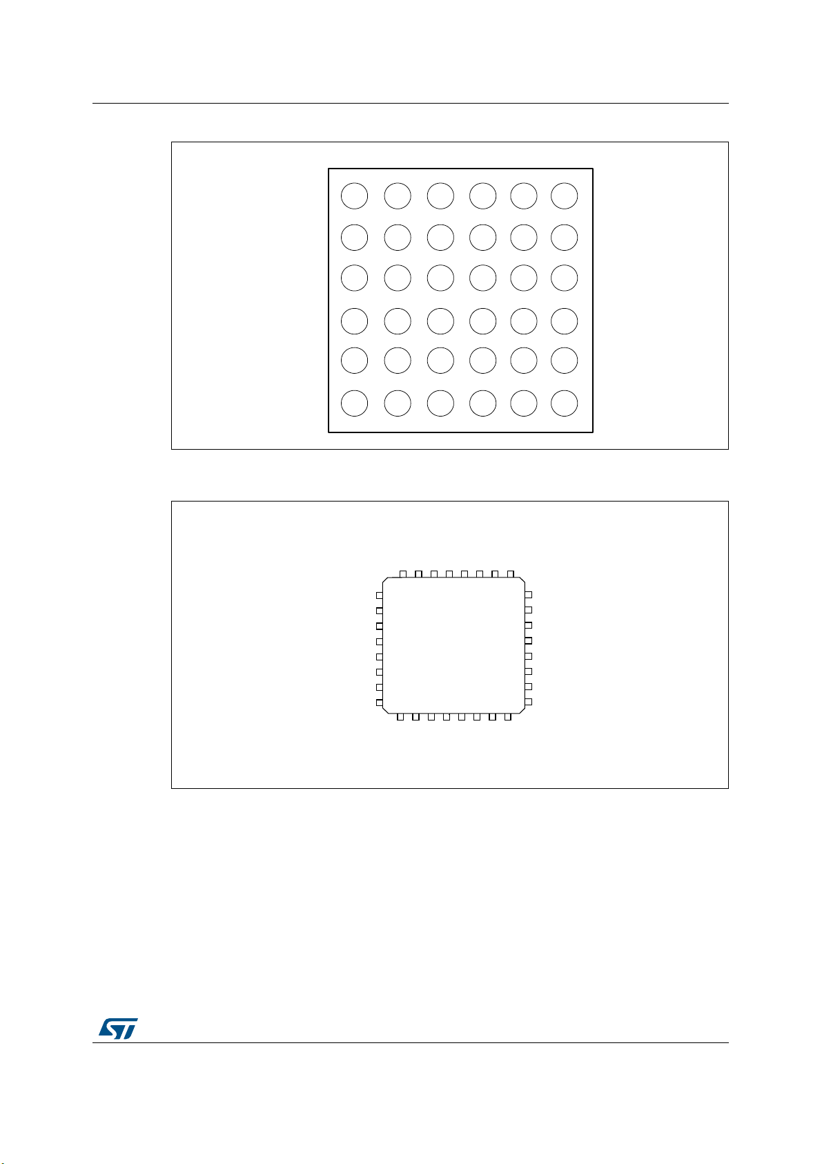
STM32L052x6 STM32L052x8 Pin descriptions
PA10
PA13
MSv37853V1
A
B
C
D
E
F
12345
6
PA12
PA9
PA8
VDD
PA15
PA14
PA11
PB11
PB10
PB2
PB4 PB7 VDD
PC14-
OSC32
_IN
PB3 PB6 PB8
PC15-
OSC32
_OUT
PB1 PB5
BOO
T0
NRST
PB0 PA0 VDDA VSS
PA6 PA4 PA 2
VREF
+
PA7
PA5
PA3
PA1
MSv35429V3
32 31 30 29 28 27 26 25
24
23
22
20
19
18
17
8
91011121
3
14 15 16
1
2
3
4
5
6
7
PA3
PA4
PA5
PA6
PA7
PB0
PB1
VSS
PA14
PA13
PA12
PA11
PA10
PA9
PA8
VDD
NRST
VDDA
PA0
PA1
PA2
VSS
BOOT0
PB7
PB6
PB5
PB4
PB3
PA15
PC14-OSC32_IN
PC15-OSC32_OUT
VDD
21
LQFP32
Figure 7. STM32L052x6/8 WLCSP36 ballout
1. The above figure shows the package top view.
Figure 8. STM32L052x6/8 LQFP32 pinout
1. The above figure shows the package top view.
DS10182 Rev 9 41/150
52
Page 42

Pin descriptions STM32L052x6 STM32L052x8
MSv37854V2
32
31 30 29 28 27 26 25
24
23
22
20
19
18
17
8
910111213
14 15 16
1
2
3
4
5
6
7
PA3
PA4
PA5
PA6
PA7
PB0
PB1
PB2
PA14
PA13
PA12
PA11
PA10
PA9
PA8
VDD
NRST
VDDA
PA0
PA1
PA2
PB8
BOOT0
PB7
PB6
PB5
PB4
PB3
PA15
PC14-OSC32_IN
PC15-OSC32_OUT
VDD
21
VSS
Figure 9. STM32L052x6/8 UFQFPN32 pinout
1. The above figure shows the package top view.
Table 15. Legend/abbreviations used in the pinout table
Name Abbreviation Definition
Pin name
Pin type
I/O structure
Notes
Pin functions
Alternate
functions
Additional
functions
Unless otherwise specified in brackets below the pin name, the pin function during and
after reset is the same as the actual pin name
S Supply pin
I Input only pin
I/O Input / output pin
FT 5 V tolerant I/O
FTf 5 V tolerant I/O, FM+ capable
TC Standard 3.3V I/O
B Dedicated BOOT0 pin
RST Bidirectional reset pin with embedded weak pull-up resistor
Unless otherwise specified by a note, all I/Os are set as floating inputs during and after
reset.
Functions selected through GPIOx_AFR registers
Functions directly selected/enabled through peripheral registers
42/150 DS10182 Rev 9
Page 43

STM32L052x6 STM32L052x8 Pin descriptions
Table 16. STM32L052x6/8 pin definitions
Pin Number
Pin name
(function after
reset)
TFBGA64
Pin type
I/O structure
Alternate functions
Notes
Additional
functions
LQFP32
UFQFN32
(1)
LQFP48
WLCSP36
LQFP64
UFQFPN48
- - - 1 1 1 B2 VDD S - - - -
RTC_TAMP1/
- - - 2 2 2 A2 PC13 I/O FT - -
RTC_TS/RTC
_OUT/WKUP2
PC14-
22A6333A1
OSC32_IN
I/O FT - - OSC32_IN
(PC14)
PC15-
33B6444B1
OSC32_OUT
I/O TC - - OSC32_OUT
(PC15)
---555C1
---666D1
PH0-OSC_IN
(PH0)
PH1-OSC_OUT
(PH1)
I/O TC - USB_CRS_SYNC OSC_IN
I/O TC - - OSC_OUT
4 4 C6 7 7 7 E1 NRST I/O RST - - -
LPTIM1_IN1,
- - - - - 8 E3 PC0 I/O FT -
EVENTOUT,
ADC_IN10
TSC_G7_IO1
LPTIM1_OUT,
- - - - - 9 E2 PC1 I/O FT -
EVENTOUT,
ADC_IN11
TSC_G7_IO2
LPTIM1_IN2,
-----10F2 PC2 I/OFT-
SPI2_MISO/I2S2_MC
ADC_IN12
K, TSC_G7_IO3
LPTIM1_ETR,
-----11- PC3 I/OFT-
SPI2_MOSI/I2S2_SD,
ADC_IN13
TSC_G7_IO4
- - - 8 8 12 F1 VSSA S - - - -
- - E6 - - - G1 VREF+ S - - - -
5 5 D5 9 9 13 H1 VDDA S - - - -
DS10182 Rev 9 43/150
52
Page 44
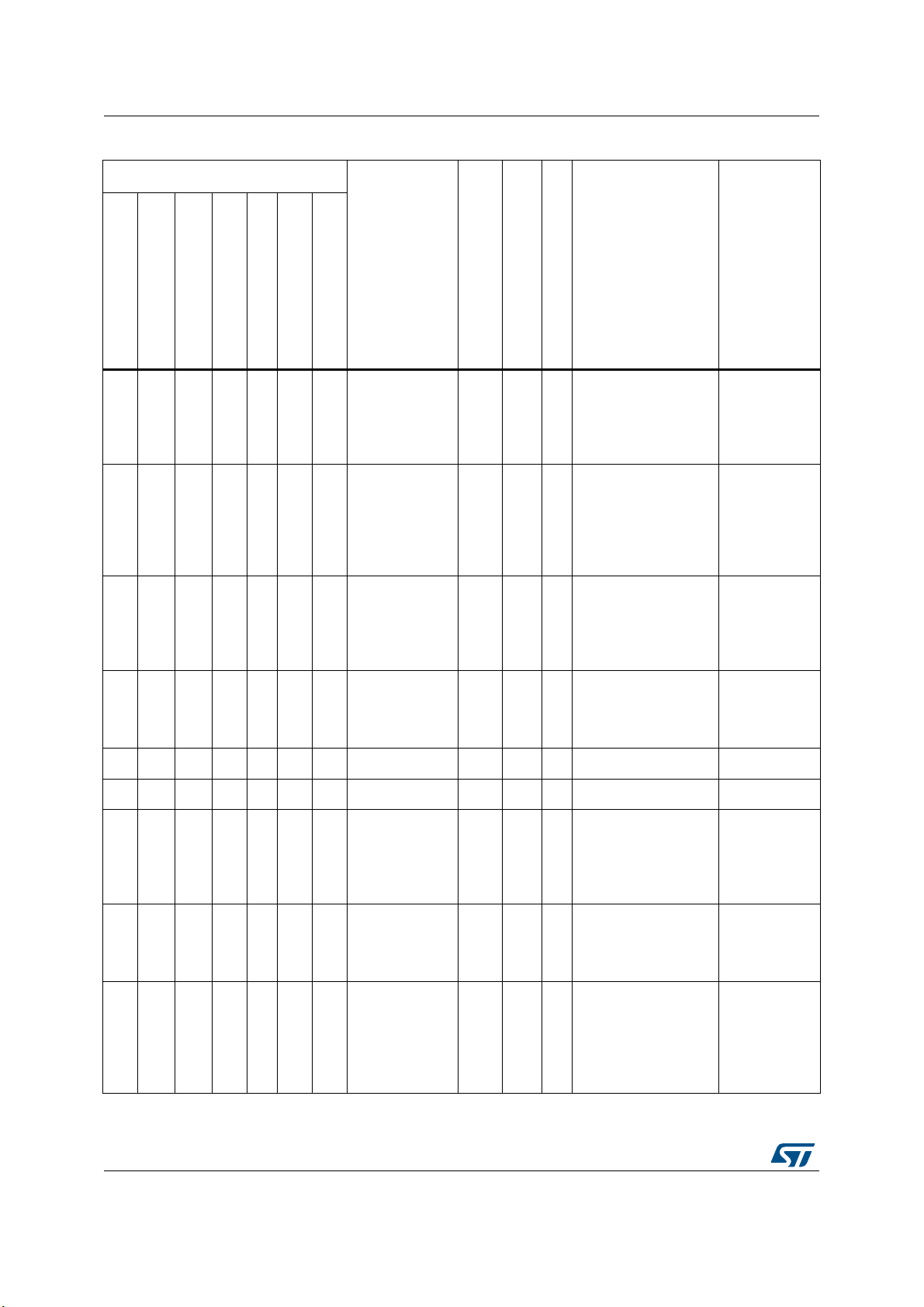
Pin descriptions STM32L052x6 STM32L052x8
Table 16. STM32L052x6/8 pin definitions (continued)
Pin Number
(1)
Pin name
(function after
reset)
LQFP32
UFQFN32
LQFP48
WLCSP36
UFQFPN48
LQFP64
TFBGA64
Pin type
Notes
I/O structure
6 6 D4 10 10 14 G2 PA0 I/O TC -
77F6111115H2 PA1 I/OFT-
8 8 E5 12 12 16 F3 PA2 I/O FT -
9 9 F5 13 13 17 G3 PA3 I/O FT -
Alternate functions
TIM2_CH1,
TSC_G1_IO1,
USART2_CTS,
TIM2_ETR,
COMP1_OUT
EVENTOUT,
TIM2_CH2,
TSC_G1_IO2,
USART2_RTS/
USART2_DE,
TIM21_ETR
TIM21_CH1,
TIM2_CH3,
TSC_G1_IO3,
USART2_TX,
COMP2_OUT
TIM21_CH2,
TIM2_CH4,
TSC_G1_IO4,
USART2_RX
Additional
functions
COMP1_INM6
, ADC_IN0,
RTC_TAMP2/
WKUP1
COMP1_INP,
ADC_IN1
COMP2_INM6
, ADC_IN2
COMP2_INP,
ADC_IN3
- - - - - 18 C2 VSS S - - - -
-----19D2 VDD S -- - -
COMP1_INM4
COMP2_INM4
, ADC_IN4,
DAC_OUT
COMP1_INM5
COMP2_INM5
, ADC_IN5
10 10 E4 14 14 20 H3 PA4 I/O TC
11 11 F4 15 15 21 F4 PA5 I/O TC -
(2)
SPI1_NSS,
TSC_G2_IO1,
USART2_CK,
TIM22_ETR
SPI1_SCK,
TIM2_ETR,
TSC_G2_IO2,
TIM2_CH1
SPI1_MISO,
TSC_G2_IO3,
12 12 E3 16 16 22 G4 PA6 I/O FT -
LPUART1_CTS,
TIM22_CH1,
ADC_IN6
EVENTOUT,
COMP1_OUT
44/150 DS10182 Rev 9
,
,
Page 45

STM32L052x6 STM32L052x8 Pin descriptions
Table 16. STM32L052x6/8 pin definitions (continued)
Pin Number
(1)
Pin name
(function after
reset)
LQFP32
UFQFN32
LQFP48
WLCSP36
UFQFPN48
LQFP64
TFBGA64
Pin type
Notes
I/O structure
13 13 F3 17 17 23 H4 PA7 I/O FT -
-----24H5 PC4 I/OFT-
-----25H6 PC5 I/OFT-
14 14 D3 18 18 26 F5 PB0 I/O FT -
15 15 C3 19 19 27 G5 PB1 I/O FT -
- 16 F2 20 20 28 G6 PB2 I/O FT -
- - E2 21 21 29 G7 PB10 I/O FT -
Alternate functions
SPI1_MOSI,
TSC_G2_IO4,
TIM22_CH2,
EVENTOUT,
COMP2_OUT
EVENTOUT,
LPUART1_TX
LPUART1_RX,
TSC_G3_IO1
EVENTOUT,
TSC_G3_IO2
TSC_G3_IO3,
LPUART1_RTS/
LPUART1_DE
LPTIM1_OUT,
TSC_G3_IO4
TIM2_CH3,
TSC_SYNC,
LPUART1_TX,
SPI2_SCK,
I2C2_SCL
Additional
functions
ADC_IN7
ADC_IN14
ADC_IN15
ADC_IN8,
VREF_OUT
ADC_IN9,
VREF_OUT
-
-
EVENTOUT,
TIM2_CH4,
- - D2 22 22 30 H7 PB11 I/O FT -
TSC_G6_IO1,
LPUART1_RX,
I2C2_SDA
16 - - 23 23 31 D6 VSS S - - - -
17 17 F1 24 24 32 E5 VDD S - - - -
SPI2_NSS/I2S2_WS,
LPUART1_RTS/
- - - 25 25 33 H8 PB12 I/O FT -
LPUART1_DE,
TSC_G6_IO2,
I2C2_SMBA,
EVENTOUT
DS10182 Rev 9 45/150
-
-
52
Page 46

Pin descriptions STM32L052x6 STM32L052x8
Table 16. STM32L052x6/8 pin definitions (continued)
Pin Number
(1)
Pin name
(function after
reset)
LQFP32
UFQFN32
LQFP48
WLCSP36
UFQFPN48
LQFP64
TFBGA64
Pin type
Notes
I/O structure
- - - 26 26 34 G8 PB13 I/O FTf -
- - - 27 27 35 F8 PB14 I/O FTf -
- - - 28 28 36 F7 PB15 I/O FT -
SPI2_MOSI/I2S2_SD,
-----37F6 PC6 I/OFT-
-----38E7 PC7 I/OFT-
-----39E8 PC8 I/OFT-
Alternate functions
SPI2_SCK/I2S2_CK,
TSC_G6_IO3,
LPUART1_CTS,
I2C2_SCL,
TIM21_CH1
SPI2_MISO/I
2S2_MCK,
RTC_OUT,
TSC_G6_IO4,
LPUART1_RTS/
LPUART1_DE,
I2C2_SDA,
TIM21_CH2
RTC_REFIN
TIM22_CH1,
TSC_G8_IO1
TIM22_CH2,
TSC_G8_IO2
TIM22_ETR,
TSC_G8_IO3
Additional
functions
-
-
-
-
-
-
-----40D8 PC9 I/OFT-
18 18 E1 29 29 41 D7 PA8 I/O FT -
19 19 D1 30 30 42 C7 PA9 I/O FT -
20 20 C1 31 31 43 C6 PA10 I/O FT -
21 21 C2 32 32 44 C8 PA11
(3)
I/O FT -
46/150 DS10182 Rev 9
TIM21_ETR,
USB_NOE,
TSC_G8_IO4
MCO,
USB_CRS_SYNC,
EVENTOUT,
USART1_CK
MCO, TSC_G4_IO1,
USART1_TX
TSC_G4_IO2,
USART1_RX
SPI1_MISO,
EVENTOUT,
TSC_G4_IO3,
USART1_CTS,
COMP1_OUT
-
-
-
-
USB_DM
Page 47

STM32L052x6 STM32L052x8 Pin descriptions
Table 16. STM32L052x6/8 pin definitions (continued)
Pin Number
(1)
LQFP32
UFQFN32
LQFP48
WLCSP36
UFQFPN48
LQFP64
Pin name
(function after
reset)
TFBGA64
Pin type
Alternate functions
Notes
Additional
functions
I/O structure
SPI1_MOSI,
EVENTOUT,
22 22 B1 33 33 45 B8 PA12
(3)
I/O FT -
TSC_G4_IO4,
USART1_RTS/
USB_DP
USART1_DE,
COMP2_OUT
23 23 A1 34 34 46 A8 PA13 I/O FT - SWDIO, USB_NOE -
- - - 35 35 47 D5 VSS S - - - -
- - - 36 36 48 E6 VDD_USB S - - - -
24 24 B2 37 37 49 A7 PA14 I/O FT - SWCLK, USART2_TX -
SPI1_NSS,
TIM2_ETR,
25 25 A2 38 38 50 A6 PA15 I/O FT -
EVENTOUT,
USART2_RX,
TIM2_CH1
-
- - - - - 51 B7 PC10 I/O FT - LPUART1_TX -
- - - - - 52 B6 PC11 I/O FT - LPUART1_RX -
-----53C5 PC12 I/OFT- - -
-----54B5 PD2 I/OFT-
LPUART1_RTS/
LPUART1_DE
-
SPI1_SCK,
26 26 B3 39 39 55 A5 PB3 I/O FT -
TIM2_CH2,
TSC_G5I_O1,
COMP2_INN
EVENTOUT
SPI1_MISO,
27 27 A3 40 40 56 A4 PB4 I/O FT -
EVENTOUT,
TSC_G5_IO2,
COMP2_INP
TIM22_CH1
SPI1_MOSI,
28 28 C4 41 41 57 C4 PB5 I/O FT -
LPTIM1_IN1,
I2C1_SMBA,
COMP2_INP
TIM22_CH2
DS10182 Rev 9 47/150
52
Page 48

Pin descriptions STM32L052x6 STM32L052x8
Table 16. STM32L052x6/8 pin definitions (continued)
Pin Number
(1)
LQFP32
UFQFN32
LQFP48
WLCSP36
UFQFPN48
LQFP64
Pin name
(function after
reset)
TFBGA64
Pin type
Alternate functions
Notes
Additional
functions
I/O structure
USART1_TX,
29 29 B4 42 42 58 D3 PB6 I/O FTf -
I2C1_SCL,
LPTIM1_ETR,
COMP2_INP
TSC_G5_IO3
USART1_RX,
30 30 A4 43 43 59 C3 PB7 I/O FTf -
I2C1_SDA,
LPTIM1_IN2,
COMP2_INP,
PVD_IN
TSC_G5_IO4
31 31 C5 44 44 60 B4 BOOT0 B - - - -
- 32 B5 45 45 61 B3 PB8 I/O FTf -
TSC_SYNC,
I2C1_SCL
EVENTOUT,
- - - 46 46 62 A3 PB9 I/O FTf -
I2C1_SDA,
SPI2_NSS/I2S2_WS
32 - D6 47 47 63 D4 VSS S - - - -
-
-
1 1 A5 48 48 64 E4 VDD S - - - -
1. PB9/12/13/14/15, PH0/1 and PC13 GPIOs should be configured as output and driven Low, even if they are not available on
this package.
2. PA4 offers a reduced touch sensing sensitivity. It is thus recommended to use it as sampling capacitor I/O.
3. These pins are powered by VDD_USB. For all characteristics that refer to V
DD
, V
must be used instead.
DD_USB
48/150 DS10182 Rev 9
Page 49

DS10182 Rev 9 49/150
Port A
Table 17. Alternate function port A
AF0 AF1 AF2 AF3 AF4 AF5 AF6 AF7
Port
SPI1/TIM21/SYS_A
F/EVENTOUT/
-
USB/TIM2/
EVENTOUT/
TSC/
EVENTOUT
USART1/2/3 TIM2/21/22 EVENTOUT COMP1/2
PA0 - - TIM2_CH1 TSC_G1_IO1 USART2_CTS TIM2_ETR - COMP1_OUT
PA1 EVENTOUT - TIM2_CH2 TSC_G1_IO2
USART2_RTS/
USART2_DE
TIM21_ETR - -
PA2 TIM21_CH1 - TIM2_CH3 TSC_G1_IO3 USART2_TX - - COMP2_OUT
PA3 TIM21_CH2 - TIM2_CH4 TSC_G1_IO4 USART2_RX - - -
PA4 SPI1_NSS - - TSC_G2_IO1 USART2_CK TIM22_ETR - -
PA5 SPI1_SCK - TIM2_ETR TSC_G2_IO2 TIM2_CH1 - -
PA6 SPI1_MISO - - TSC_G2_IO3 LPUART1_CTS TIM22_CH1 EVENTOUT COMP1_OUT
PA7 SPI1_MOSI - - TSC_G2_IO4 TIM22_CH2 EVENTOUT COMP2_OUT
PA8 MCO - USB_CRS_SYNC EVENTOUT USART1_CK - - -
PA9 MCO - - TSC_G4_IO1 USART1_TX - - -
PA10 - - - TSC_G4_IO2 USART1_RX - - -
PA11 SPI1_MISO - EVENTOUT TSC_G4_IO3 USART1_CTS - - COMP1_OUT
PA12 SPI1_MOSI - EVENTOUT TSC_G4_IO4
USART1_RTS/
USART1_DE
- - COMP2_OUT
PA13 SWDIO - USB_NOE - - - - -
PA14 SWCLK - - - USART2_TX - - -
STM32L052x6 STM32L052x8 Pin descriptions
PA15 SPI1_NSS - TIM2_ETR EVENTOUT USART2_RX TIM2_CH1 - -
Page 50

50/150 DS10182 Rev 9
Pin descriptions STM32L052x6 STM32L052x8
Table 18. Alternate function port B
AF0 AF1 AF2 AF3 AF4 AF5 AF6
Port B
Port
PB0 EVENTOUT - - TSC_G3_IO2 - - -
PB1 - - - TSC_G3_IO3
PB2 - - LPTIM1_OUT TSC_G3_IO4 - - -
PB3 SPI1_SCK - TIM2_CH2 TSC_G5I_O1 EVENTOUT - -
PB4 SPI1_MISO - EVENTOUT TSC_G5_IO2 TIM22_CH1 - -
PB5 SPI1_MOSI - LPTIM1_IN1 I2C1_SMBA TIM22_CH2 - -
PB6 USART1_TX I2C1_SCL LPTIM1_ETR TSC_G5_IO3 - - -
PB7 USART1_RX I2C1_SDA LPTIM1_IN2 TSC_G5_IO4 - - -
PB8 - - - TSC_SYNC I2C1_SCL - -
PB9 - - EVENTOUT - I2C1_SDA
PB10 - - TIM2_CH3 TSC_SYNC LPUART1_TX SPI2_SCK I2C2_SCL
PB11 EVENTOUT - TIM2_CH4 TSC_G6_IO1 LPUART1_RX I2C2_SDA
PB12 SPI2_NSS/I2S2_WS -
PB13 SPI2_SCK/I2S2_CK - - TSC_G6_IO3 LPUART1_CTS I2C2_SCL TIM21_CH1
SPI1/SPI2/I2S2/
USART1/
EVENTOUT/
I2C1
LPUART1/LPTIM
/TIM2/SYS_AF/
EVENTOUT
LPUART1_RTS/
LPUART1_DE
I2C1/TIM22/
I2C1/TSC
TSC_G6_IO2 - I2C2_SMBA EVENTOUT
EVENTOUT/
LPUART1
LPUART1_RTS/
LPUART1_DE
SPI2/I2S2/I2C2
--
SPI2_NSS/I2S2_
WS
I2C2/TIM21/
EVENTOUT
-
PB14 SPI2_MISO/I2S2_MCK - RTC_OUT TSC_G6_IO4
PB15 SPI2_MOSI/I2S2_SD - RTC_REFIN - - - -
LPUART1_RTS/
LPUART1_DE
I2C2_SDA TIM21_CH2
Page 51

Table 19. Alternate function port C
AF0 AF1 AF2 AF3
STM32L052x6 STM32L052x8 Pin descriptions
DS10182 Rev 9 51/150
Port C
Port
PC0 LPTIM1_IN1 - EVENTOUT TSC_G7_IO1
PC1 LPTIM1_OUT - EVENTOUT TSC_G7_IO2
PC2 LPTIM1_IN2 - SPI2_MISO/I2S2_MCK TSC_G7_IO3
PC3 LPTIM1_ETR - SPI2_MOSI/I2S2_SD TSC_G7_IO4
PC4 EVENTOUT - LPUART1_TX -
PC5 - - LPUART1_RX TSC_G3_IO1
PC6 TIM22_CH1 - - TSC_G8_IO1
PC7 TIM22_CH2 - - TSC_G8_IO2
PC8 TIM22_ETR - - TSC_G8_IO3
PC9 TIM21_ETR - USB_NOE TSC_G8_IO4
PC10 LPUART1_TX - - -
PC11 LPUART1_RX - - -
PC12----
PC13----
PC14----
LPUART1/LPTIM/
TIM21/12/
EVENTOUT/
-
SPI2/I2S2/USB/
LPUART1/
EVENTOUT
TSC
PC15----
Page 52

52/150 DS10182 Rev 9
Pin descriptions STM32L052x6 STM32L052x8
Table 20. Alternate function port D
AF0
Port
LPUART1
Port D PD2 LPUART1_RTS/LPUART1_DE
Table 21. Alternate function port H
AF0
Port
USB
Port H
PH0 USB_CRS_SYNC
PH1 -
Page 53

STM32L052x6 STM32L052x8 Memory mapping
5 Memory mapping
Refer to the product line reference manual for details on the memory mapping as well as the
boundary addresses for all peripherals.
DS10182 Rev 9 53/150
53
Page 54
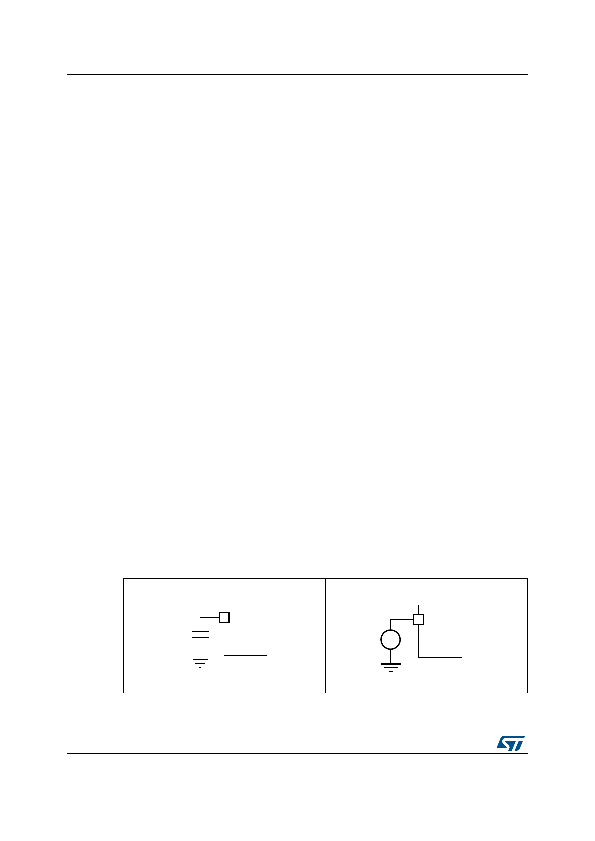
Electrical characteristics STM32L052x6 STM32L052x8
ai17851c
C = 50 pF
MCU pin
ai17852c
MCU pin
V
IN
6 Electrical characteristics
6.1 Parameter conditions
Unless otherwise specified, all voltages are referenced to VSS.
6.1.1 Minimum and maximum values
Unless otherwise specified the minimum and maximum values are guaranteed in the worst
conditions of ambient temperature, supply voltage and frequencies by tests in production on
100% of the devices with an ambient temperature at T
the selected temperature range).
Data based on characterization results, design simulation and/or technology characteristics
are indicated in the table footnotes and are not tested in production. Based on
characterization, the minimum and maximum values refer to sample tests and represent the
mean value plus or minus three times the standard deviation (mean±3σ).
6.1.2 Typical values
Unless otherwise specified, typical data are based on TA = 25 °C, VDD = 3.6 V (for the
1.65 V ≤ V
tested.
≤ 3.6 V voltage range). They are given only as design guidelines and are not
DD
= 25 °C and TA = TAmax (given by
A
Typical ADC accuracy values are determined by characterization of a batch of samples from
a standard diffusion lot over the full temperature range, where 95% of the devices have an
error less than or equal to the value indicated
6.1.3 Typical curves
Unless otherwise specified, all typical curves are given only as design guidelines and are
not tested.
6.1.4 Loading capacitor
The loading conditions used for pin parameter measurement are shown in Figure 10.
6.1.5 Pin input voltage
The input voltage measurement on a pin of the device is described in Figure 11.
Figure 10. Pin loading conditions Figure 11. Pin input voltage
(mean±2σ).
54/150 DS10182 Rev 9
Page 55

STM32L052x6 STM32L052x8 Electrical characteristics
MSv34738V1
Analog:
RC,PLL,COMP,
….
V
DD
GP I/Os
OUT
IN
Kernel logic
(CPU,
Digital &
Memories)
Standby-power circuitry
(OSC32,RTC,Wake-up
logic, RTC backup
registers)
N × 100 nF
+ 1 × 10 μF
Regulator
V
SS
V
DDA
V
REF+
V
REF-
V
SSA
ADC/
DAC
Level shifter
IO
Logic
V
DD
100 nF
+ 1 μF
V
REF
100 nF
+ 1 μF
V
DDA
V
DD_USB
USB
transceiver
V
SS
MSv34711V1
NxVDD
IDD
N × 100 nF
+ 1 × 10 μF
NxVSS
VDDA
6.1.6 Power supply scheme
Figure 12. Power supply scheme
6.1.7 Current consumption measurement
Figure 13. Current consumption measurement scheme
DS10182 Rev 9 55/150
114
Page 56

Electrical characteristics STM32L052x6 STM32L052x8
6.2 Absolute maximum ratings
Stresses above the absolute maximum ratings listed in Table 22: Voltage characteristics,
Table 23: Current characteristics, and Table 24: Thermal characteristics may cause
permanent damage to the device. These are stress ratings only and functional operation of
the device at these conditions is not implied. Exposure to maximum rating conditions for
extended periods may affect device reliability. Device mission profile (application conditions)
is compliant with JEDEC JESD47 Qualification Standard. Extended mission profiles are
available on demand.
Symbol Definition Min Max Unit
Table 22. Voltage characteristics
VDD–V
(2)
V
IN
|ΔV
DD
DDA-VDDx
External main supply voltage
SS
(including V
DDA
, V
DD_USB
, VDD)
(1)
Input voltage on FT and FTf pins V
Input voltage on TC pins V
Input voltage on BOOT0 V
Input voltage on any other pin V
| Variations between different V
Variations between any V
|
(3)
pins
DDx
power pins - 50
DDx
and V
DDA
power
–0.3 4.0
− 0.3 VDD+4.0
SS
− 0.3 4.0
SS
SS
− 0.3 4.0
SS
- 300
|ΔVSS| Variations between all different ground pins - 50
V
REF+ –VDDA
V
ESD(HBM)
1. All main power (VDD,V
external power supply, in the permitted range.
2. V
maximum must always be respected. Refer to Table 23 for maximum allowed injected current values.
IN
3. It is recommended to power VDD and V
between V
from V
Allowed voltage difference for V
Electrostatic discharge voltage
(human body model)
, V
DD_USB
DD
and V
DD
and V
can be tolerated during power-up and device operation. V
DDA
: its value does not need to respect this rule.
DDA
) and ground (VSS, V
DDA
from the same source. A maximum difference of 300 mV
DDA
REF+
> V
DDA
-0.4V
see Section 6.3.11
) pins must always be connected to the
SSA
DD_USB
V
VDD + 4.0
mV|V
is independent
56/150 DS10182 Rev 9
Page 57
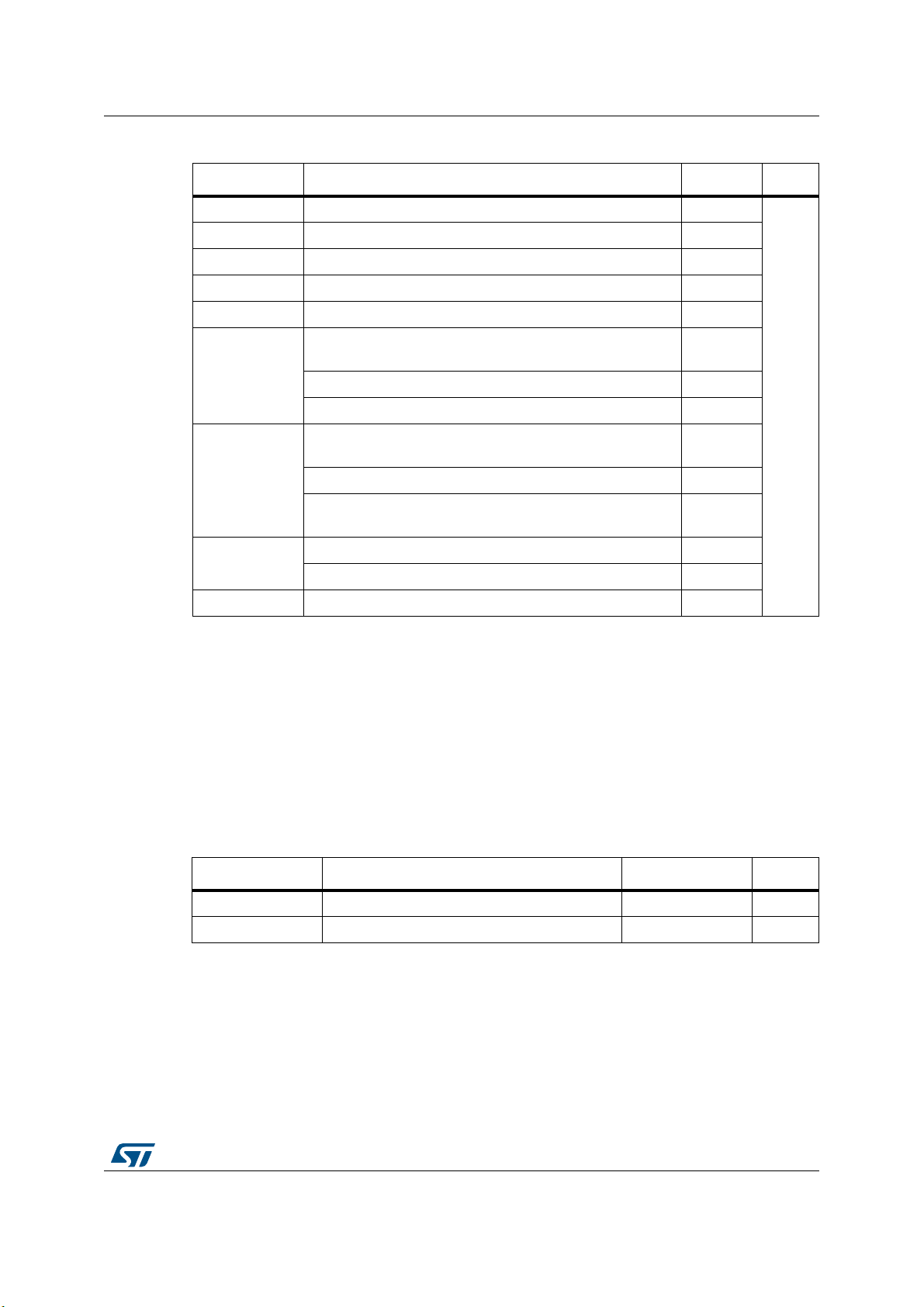
STM32L052x6 STM32L052x8 Electrical characteristics
Table 23. Current characteristics
Symbol Ratings Max. Unit
(1)
(1)
(1)
(1)
105
105
100
100
16
ΣI
VDD
ΣI
VSS
ΣI
VDD_USB
I
VDD(PIN)
I
VSS(PIN)
I
IO
(2)
(2)
Total current into sum of all VDD power lines (source)
Total current out of sum of all VSS ground lines (sink)
Total current into V
power lines (source) 25
DD_USB
Maximum current into each VDD power pin (source)
Maximum current out of each VSS ground pin (sink)
Output current sunk by any I/O and control pin except FTf
pins
Output current sunk by FTf pins 22
Output current sourced by any I/O and control pin -16
ΣI
IO(PIN)
Total output current sunk by sum of all IOs and control pins
except PA11 and PA12
Total output current sunk by PA11 and PA12 25
Total output current sourced by sum of all IOs and control
(2)
pins
(2)
Injected current on FT, FTf, RST and B pins -5/+0
I
INJ(PIN)
ΣI
INJ(PIN)
1. All main power (VDD, V
supply, in the permitted range.
2. This current consumption must be correctly distributed over all I/Os and control pins. The total output
current must not be sunk/sourced between two consecutive power supply pins referring to high pin count
LQFP packages.
3. Positive current injection is not possible on these I/Os. A negative injection is induced by VIN<VSS. I
must never be exceeded. Refer to Table 22 for maximum allowed input voltage values.
4. A positive injection is induced by V
must never be exceeded. Refer to Table 22: Voltage characteristics for the maximum allowed input voltage
values.
5. When several inputs are submitted to a current injection, the maximum ΣI
positive and negative injected currents (instantaneous values).
Injected current on TC pin ± 5
Total injected current (sum of all I/O and control pins)
) and ground (VSS, V
DDA
> VDD while a negative injection is induced by V
IN
) pins must always be connected to the external power
SSA
(5)
is the absolute sum of the
INJ(PIN)
< VSS. I
IN
90
-90
± 25
(3)
(4)
INJ(PIN)
mA
INJ(PIN)
Table 24. Thermal characteristics
Symbol Ratings Value Unit
T
STG
T
J
Storage temperature range –65 to +150 °C
Maximum junction temperature 150 °C
DS10182 Rev 9 57/150
114
Page 58

Electrical characteristics STM32L052x6 STM32L052x8
6.3 Operating conditions
6.3.1 General operating conditions
Table 25. General operating conditions
Symbol Parameter Conditions Min Max Unit
f
HCLK
PCLK1
f
PCLK2
Internal AHB clock frequency - 0 32
Internal APB1 clock frequency - 0 32
Internal APB2 clock frequency - 0 32
MHzf
BOR detector disabled 1.65 3.6
V
Standard operating voltage
DD
VBOR detector enabled, at power-on 1.8 3.6
BOR detector disabled, after power-on 1.65 3.6
V
V
V
USB
DDA
DDA
DD_
V
Analog operating voltage (DAC not
used)
Analog operating voltage (all
features)
Standard operating voltage, USB
(2)
domain
Input voltage on FT, FTf and RST
(3)
pins
IN
Input voltage on BOOT0 pin - 0 5.5
Must be the same voltage as V
Must be the same voltage as V
USB peripheral used 3.0 3.6
USB peripheral not used 0 3.6
2.0 V ≤ VDD ≤ 3.6 V -0.3 5.5
1.65 V ≤ V
≤ 2.0 V -0.3 5.2
DD
DD
DD
(1)
(1)
1.65 3.6 V
1.8 3.6 V
V
V
Input voltage on TC pin - -0.3 VDD+0.3
TFBGA64 package - 327
LQFP64 package - 444
LQFP48 package - 363
Power dissipation at T
(range 6) or T
=105 °C (rage 7)
A
= 85 °C
A
Standard WLCSP36 package - 318
(4)
Thin WLCSP36 package - 338
LQFP32 package - 351
UFQFPN32 - 526
UFQFPN48 - 654
P
D
TFBGA64 package - 81
LQFP64 package - 111
LQFP48 package - 91
Power dissipation at T
(range 3)
(4)
= 125 °C
A
Standard WLCSP36 package - 79
Thin WLCSP36 package - 84
LQFP32 package - 88
UFQFPN32 - 132
UFQFPN48 - 163
58/150 DS10182 Rev 9
mW
Page 59

STM32L052x6 STM32L052x8 Electrical characteristics
Table 25. General operating conditions (continued)
Symbol Parameter Conditions Min Max Unit
Maximum power dissipation (range 6) –40 85
TA Temperature range
Maximum power dissipation (range 7) –40 105
Maximum power dissipation (range 3) –40 125
Junction temperature range (range 6) -40 °C ≤ T
Junction temperature range (range 7) -40 °C ≤ T
J
T
Junction temperature range (range 3) -40 °C ≤ T
1. It is recommended to power VDD and V
can be tolerated during power-up and normal operation.
2. V
- When V
- When VDD is powered-down (VDD < V
- In operating mode, V
- If the USB is not used, V
- If the USB is not used and PA11/PA12 are not used as standard I/Os, VDD_USB must be connected to a VSS or VDD power
must respect the following conditions:
DD_USB
is powered-on (VDD < V
DD
DD_USB
DD_USB
could be lower or higher V
must range from V
supply voltage (VDD_USB must not be left floating).
3. To sustain a voltage higher than V
4. If T
is lower, higher PD values are allowed as long as TJ does not exceed TJ max (see Table 24: Thermal characteristics on
A
page 57).
DD
from the same source. A maximum difference of 300 mV between VDD and V
DDA
DD_min
DD_min
), V
should be always lower than V
DD_USB
), V
DD_USB
DD_min
+0.3V, the internal pull-up/pull-down resistors must be disabled.
≤ 85 ° –40 105
A
≤ 105 °C –40 125
A
≤ 125 °C –40 130
A
should be always lower than V
DD.
to V
to be able to use PA11 and PA12 as standard I/Os.
DD_max
DD.
DD.
DDA
°C
DS10182 Rev 9 59/150
114
Page 60

Electrical characteristics STM32L052x6 STM32L052x8
6.3.2 Embedded reset and power control block characteristics
The parameters given in the following table are derived from the tests performed under the
ambient temperature condition summarized in Table 25.
Table 26. Embedded reset and power control block characteristics
Symbol Parameter Conditions Min Typ Max Unit
t
VDD
T
RSTTEMPO
V
POR/PDR
V
BOR0
V
BOR1
V
BOR2
V
BOR3
V
BOR4
V
PVD0
V
PVD1
V
PVD2
VDD rise time rate
(1)
V
fall time rate
DD
(1)
Reset temporization
Power-on/power down reset
threshold
Brown-out reset threshold 0
Brown-out reset threshold 1
Brown-out reset threshold 2
Brown-out reset threshold 3
Brown-out reset threshold 4
Programmable voltage detector
threshold 0
PVD threshold 1
PVD threshold 2
BOR detector enabled 0 -
∞
BOR detector disabled 0 - 1000
BOR detector enabled 20 - ∞
BOR detector disabled 0 - 1000
VDD rising, BOR enabled - 2 3.3
rising, BOR disabled
V
DD
(2)
0.4 0.7 1.6
Falling edge 1 1.5 1.65
Rising edge 1.3 1.5 1.65
Falling edge 1.67 1.7 1.74
Rising edge 1.69 1.76 1.8
Falling edge 1.87 1.93 1.97
Rising edge 1.96 2.03 2.07
Falling edge 2.22 2.30 2.35
Rising edge 2.31 2.41 2.44
Falling edge 2.45 2.55 2.6
Rising edge 2.54 2.66 2.7
Falling edge 2.68 2.8 2.85
Rising edge 2.78 2.9 2.95
Falling edge 1.8 1.85 1.88
Rising edge 1.88 1.94 1.99
Falling edge 1.98 2.04 2.09
Rising edge 2.08 2.14 2.18
Falling edge 2.20 2.24 2.28
Rising edge 2.28 2.34 2.38
µs/V
ms
V
V
PVD3
PVD threshold 3
Rising edge 2.47 2.54 2.58
Falling edge 2.57 2.64 2.69
Falling edge 2.39 2.44 2.48
V
PVD4
PVD threshold 4
Rising edge 2.68 2.74 2.79
Falling edge 2.77 2.83 2.88
V
PVD5
PVD threshold 5
Rising edge 2.87 2.94 2.99
60/150 DS10182 Rev 9
Page 61

STM32L052x6 STM32L052x8 Electrical characteristics
Table 26. Embedded reset and power control block characteristics (continued)
Symbol Parameter Conditions Min Typ Max Unit
V
PVD6
PVD threshold 6
Rising edge 3.08 3.15 3.20
BOR0 threshold - 40 -
Falling edge 2.97 3.05 3.09
V
hyst
1. Guaranteed by characterization results.
2. Valid for device version without BOR at power up. Please see option "D" in Ordering information scheme for more details.
Hysteresis voltage
All BOR and PVD thresholds
excepting BOR0
-100-
6.3.3 Embedded internal reference voltage
The parameters given in Table 28 are based on characterization results, unless otherwise
specified.
VREFINT_CAL
Symbol Parameter Conditions Min Typ
VREFINT
(4)
Coeff
(4)
Coeff
(4)(5)
(2)
(4)
V
REFINT out
T
V
VREF_MEAS
A
VREF_MEAS
T
A
V
DDCoeff
T
S_vrefint
Table 27. Embedded internal reference voltage calibration values
Calibration value name Description Memory address
Raw data acquired at
temperature of 25 °C
V
= 3 V
DDA
Table 28. Embedded internal reference voltage
Internal reference voltage – 40 °C < TJ < +125 °C 1.202 1.224 1.242 V
Internal reference startup time - - 2 3 ms
V
and V
DDA
V
factory measure
REFINT
Accuracy of factory-measured
REFINT
value
V
Temperature coefficient –40 °C < TJ < +125 °C - 25 100 ppm/°C
Long-term stability 1000 hours, T= 25 °C - - 1000 ppm
Voltage coefficient 3.0 V < V
ADC sampling time when
reading the internal reference
voltage
voltage during
REF+
(3)
-2.9933.01V
Including uncertainties
due to ADC and
V
DDA/VREF+
values
< 3.6 V - - 2000 ppm/V
DDA
-510-µs
0x1FF8 0078 - 0x1FF8 0079
(1)
Max Unit
-- ±5mV
V
mV
T
ADC_BUF
I
BUF_ADC
I
VREF_OUT
C
VREF_OUT
Startup time of reference
(4)
voltage buffer for ADC
Consumption of reference
(4)
voltage buffer for ADC
(4)
VREF_OUT output current
(4)
VREF_OUT output load - - - 50 pF
(6)
---10µs
- - 13.5 25 µA
---1µA
DS10182 Rev 9 61/150
114
Page 62

Electrical characteristics STM32L052x6 STM32L052x8
Table 28. Embedded internal reference voltage
Symbol Parameter Conditions Min Typ
Consumption of reference
voltage buffer for VREF_OUT
- - 730 1200 nA
I
LPBUF
(4)
(1)
(continued)
Max Unit
and COMP
(4)
V
REFINT_DIV1
V
REFINT_DIV2
V
REFINT_DIV3
1. Refer to Table 40: Peripheral current consumption in Stop and Standby mode for the value of the internal reference current
consumption (I
2. Guaranteed by test in production.
3. The internal V
4. Guaranteed by design.
5. Shortest sampling time can be determined in the application by multiple iterations.
6. To guarantee less than 1% VREF_OUT deviation.
1/4 reference voltage - 24 25 26
(4)
1/2 reference voltage - 49 50 51
(4)
3/4 reference voltage - 74 75 76
REFINT).
value is individually measured in production and stored in dedicated EEPROM bytes.
REF
V
REFINT
%
6.3.4 Supply current characteristics
The current consumption is a function of several parameters and factors such as the
operating voltage, temperature, I/O pin loading, device software configuration, operating
frequencies, I/O pin switching rate, program location in memory and executed binary code.
The current consumption is measured as described in Figure 13: Current consumption
measurement scheme.
All Run-mode current consumption measurements given in this section are performed with a
reduced code that gives a consumption equivalent to Dhrystone 2.1 code if not specified
otherwise.
The current consumption values are derived from the tests performed under ambient
temperature and V
supply voltage conditions summarized in Table 25: General operating
DD
conditions unless otherwise specified.
The MCU is placed under the following conditions:
• All I/O pins are configured in analog input mode
• All peripherals are disabled except when explicitly mentioned
• The Flash memory access time and prefetch is adjusted depending on fHCLK
frequency and voltage range to provide the best CPU performance unless otherwise
specified.
• When the peripherals are enabled f
APB1
= f
APB2
= f
APB
• When PLL is ON, the PLL inputs are equal to HSI = 16 MHz (if internal clock is used) or
HSE = 16 MHz (if HSE bypass mode is used)
• The HSE user clock applied to OSCI_IN input follows the characteristic specified in
Table 42: High-speed external user clock characteristics
• For maximum current consumption V
• For typical current consumption V
DD
DD
= V
= V
DDA
= 3.6 V is applied to all supply pins
DDA
= 3.0 V is applied to all supply pins if not
specified otherwise
The parameters given in Table 50, Table 25 and Table 26 are derived from tests performed
under ambient temperature and V
supply voltage conditions summarized in Table 25.
DD
62/150 DS10182 Rev 9
Page 63

STM32L052x6 STM32L052x8 Electrical characteristics
Table 29. Current consumption in Run mode, code with data processing running from Flash
Symbol Parameter Conditions f
HCLK
Typ M ax
(1)
1 MHz 165 230
Range 3, V
CORE
=1.2 V
VOS[1:0]=11
4 MHz 555 630
f
HSE
= f
HCLK
up to
16 MHz included,
f
HSE
= f
HCLK
/2 above
16 MHz (PLL ON)
Range 2, V
VOS[1:0]=10,
(2)
CORE
=1.5 V,
4 MHz 0.665 0.74
8 MHz 1.3 1.4
16 MHz 2.6 2.8
Supply
I
DD
(Run
from
Flash)
current in
Run mode,
code
executed
from Flash
MSI clock
Range 1, V
VOS[1:0]=01
Range 3, V
VOS[1:0]=11
CORE
CORE
=1.8 V,
=1.2 V,
8 MHz 1.55 1.7
16 MHz 3.1 3.4
32 MHz 6.3 6.8
65 kHz 36.5 110
4.2 MHz 620 700
Range 2, V
VOS[1:0]=10,
CORE
=1.5 V,
16 MHz 2.6 2.9
HSI clock
Range 1, V
VOS[1:0]=01
1. Guaranteed by characterization results at 125 °C, unless otherwise specified.
2. Oscillator bypassed (HSEBYP = 1 in RCC_CR register).
CORE
=1.8 V,
32 MHz 6.25 7
Unit
µA2 MHz 290 360
mA
µA524 kHz 99.5 190
mA
Table 30. Current consumption in Run mode vs code type,
code with data processing running from Flash
Symbol Parameter Conditions f
Dhrystone
CoreMark 585
Range 3,
V
CORE
VOS[1:0]=11
Supply
I
DD
(Run
from
Flash)
current in
Run mode,
code
executed
f
HSE
= f
HCLK
up to
16 MHz included,
f
HSE
= f
HCLK
/2 above
16 MHz (PLL ON)
(1)
from Flash
Range 1,
V
CORE
VOS[1:0]=01
1. Oscillator bypassed (HSEBYP = 1 in RCC_CR register).
=1.2 V,
=1.8 V,
Fibonacci 440
while(1) 355
while(1), prefetch
OFF
Dhrystone
CoreMark 6.3
Fibonacci 6.55
while(1) 5.4
while(1), prefetch
OFF
HCLK
4 MHz
32 MHz
Typ U nit
555
µA
353
6.3
mA
5.2
DS10182 Rev 9 63/150
114
Page 64

Electrical characteristics STM32L052x6 STM32L052x8
MSv34792V1
Dhrystone 2.1 - 1 WS - 55°C
Dhrystone 2.1- 1 WS - 85°C
Dhrystone 2.1- 1 WS – 25°C
Dhrystone 2.1- 1 WS - 105°C
0
0.50
1.00
1.50
2.00
2.50
3.00
1.80E+00 2.00E+00 2.20E+00 2.40E+00 2.60E+00 2.80E+00 3.00E+00 3.20E+00 3.40E+00 3.60E+00
IDD (mA)
VDD (V)
MSv34793V1
IDD (mA)
VDD (V)
Dhrystone 2.1 - 1 WS - 55°C
Dhrystone 2.1- 1 WS - 85°C
Dhrystone 2.1- 1 WS – 25°C
Dhrystone 2.1- 1 WS - 105°C
0
0.50
1.00
1.50
2.00
2.50
3.00
1.80E+00 2.00E+00 2.20E+00 2.40E+00 2.60E+00 2.80E+00 3.00E+00 3.20E+00 3.40E+00 3.60E+00
Figure 14. IDD vs VDD, at TA= 25/55/85/105 °C, Run mode, code running from
Flash memory, Range 2, HSE, 1WS
Figure 15. I
vs VDD, at TA= 25/55/85/105 °C, Run mode, code running from
DD
Flash memory, Range 2, HSI16, 1WS
64/150 DS10182 Rev 9
Page 65

STM32L052x6 STM32L052x8 Electrical characteristics
Table 31. Current consumption in Run mode, code with data processing running from RAM
Symbol Parameter Conditions f
Range 3,
=1.2 V,
V
CORE
VOS[1:0]=11
(Run
I
DD
from
RAM)
Supply current in
Run mode, code
executed from
RAM, Flash
switched off
= f
f
HSE
MHz included,
f
= f
HSE
16 MHz (PLL ON)
up to 16
HCLK
/2 above
HCLK
MSI clock
Range 2,
V
CORE
VOS[1:0]=10
(2)
Range 1,
V
CORE
VOS[1:0]=01
Range 3,
V
CORE
=1.5 ,V,
=1.8 V,
=1.2 V,
VOS[1:0]=11
Range 2,
=1.5 V,
V
CORE
HSI16 clock source
(16 MHz)
VOS[1:0]=10
Range 1,
=1.8 V,
V
CORE
VOS[1:0]=01
HCLK
Typ M ax
1 MHz 135 170
4 MHz 450 480
4 MHz 0.52 0.6
8 MHz 1 1.2
16 MHz 2 2.3
8 MHz 1.25 1.4
16 MHz 2.45 2.8
32 MHz 5.1 5.4
65 kHz 34.5 75
4.2 MHz 485 540
16 MHz 2.1 2.3
32 MHz 5.1 5.6
(1)
Unit
µA2 MHz 240 270
mA
µA524 kHz 83 120
mA
1. Guaranteed by characterization results at 125 °C, unless otherwise specified.
2. Oscillator bypassed (HSEBYP = 1 in RCC_CR register).
Table 32. Current consumption in Run mode vs code type,
code with data processing running from RAM
Symbol Parameter Conditions f
Range 3,
V
=1.2 V,
CORE
Supply current in
IDD (Run
from
RAM)
Run mode, code
executed from
RAM, Flash
switched off
1. Guaranteed by characterization results, unless otherwise specified.
2. Oscillator bypassed (HSEBYP = 1 in RCC_CR register).
f
HSE
= f
HCLK
up to
16 MHz included,
f
HSE
= f
HCLK
/2 above
16 MHz (PLL ON)
VOS[1:0]=11
(2)
Range 1,
V
VOS[1:0]=01
CORE
=1.8 V,
(1)
Dhrystone
CoreMark 575
Fibonacci 370
while(1) 340
Dhrystone
CoreMark 6.25
Fibonacci 4.4
while(1) 4.7
HCLK
4 MHz
32 MHz
Typ U nit
450
µA
5.1
mA
DS10182 Rev 9 65/150
114
Page 66

Electrical characteristics STM32L052x6 STM32L052x8
Table 33. Current consumption in Sleep mode
Symbol Parameter Conditions f
Range 3,
=1.2 V,
V
CORE
VOS[1:0]=11
= f
f
HSE
16 MHz included,
f
= f
HSE
16 MHz (PLL ON)
HCLK
HCLK
up to
/2 above
(2)
Range 2,
=1.5 V,
V
CORE
VOS[1:0]=10
Range 1,
Supply current
in Sleep
mode, Flash
=1.8 V,
V
CORE
VOS[1:0]=01
OFF
Range 3,
MSI clock
V
CORE
=1.2 V,
VOS[1:0]=11
Range 2,
=1.5 V,
V
CORE
HSI16 clock source
(16 MHz)
VOS[1:0]=10
Range 1,
V
=1.8 V,
CORE
VOS[1:0]=01
IDD (Sleep)
Range 3,
V
=1.2 V,
CORE
VOS[1:0]=11
HCLK
Typ Max
1 MHz 43.5 90
2 MHz 72 120
4 MHz 130 180
4 MHz 160 210
8 MHz 305 370
16 MHz 590 710
8 MHz 370 430
16 MHz 715 860
32 MHz 1650 1900
65 kHz 18 65
524 kHz 31.5 75
4.2 MHz 140 210
16 MHz 665 830
32 MHz 1750 2100
1 MHz 57.5 130
2 MHz 84 170
4 MHz 150 280
(1)
Unit
µA
Supply current
in Sleep
= f
f
HSE
16 MHz included,
= f
f
HSE
16 MHz (PLL ON)
HCLK
HCLK
up to
/2 above
(2)
Range 2,
=1.5 V,
CORE
VOS[1:0]=10
Range 1,
=1.8 V,
V
CORE
VOS[1:0]=01
mode, Flash
ON
Range 3,
MSI clock
V
CORE
=1.2 V,
VOS[1:0]=11
Range 2,
=1.5 V,
V
CORE
HSI16 clock source
(16 MHz)
VOS[1:0]=10
Range 1,
V
=1.8 V,
CORE
VOS[1:0]=01
1. Guaranteed by characterization results at 125 °C, unless otherwise specified.
66/150 DS10182 Rev 9
4 MHz 170 310
8 MHz 315 420
16 MHz 605 770
8 MHz 380 460
16 MHz 730 950
32 MHz 1650 2400
65 kHz 29.5 110
524 kHz 44.5 130
4.2 MHz 150 270
16 MHz 680 950
32 MHz 1750 2100
Page 67

STM32L052x6 STM32L052x8 Electrical characteristics
2. Oscillator bypassed (HSEBYP = 1 in RCC_CR register).
Table 34. Current consumption in Low-power run mode
Symbol Parameter Conditions Typ Max
T
= − 40 to 25°C 8.5 10
A
T
= 85 °C 11.5 48
MSI clock = 65 kHz,
= 32 kHz
f
HCLK
All peripherals
OFF, code
executed from
RAM, Flash
MSI clock= 65 kHz,
f
= 65 kHz
HCLK
switched off,
from 1.65
V
DD
to 3.6 V
MSI clock= 131 kHz,
f
= 131 kHz
HCLK
Supply
I
DD
(LP Run)
current in
Low-power
run mode
MSI clock= 65 kHz,
f
= 32 kHz
HCLK
All peripherals
OFF, code
executed from
Flash, V
MSI clock = 65 kHz,
f
HCLK
DD
= 65 kHz
from 1.65 V to
3.6 V
MSI clock =
131 kHz,
= 131 kHz
f
HCLK
1. Guaranteed by characterization results at 125 °C, unless otherwise specified.
A
T
= 105 °C 15.5 53
A
= 125 °C 27.5 130
T
A
T
=-40 °C to 25 °C 10 15
A
T
= 85 °C 15.5 50
A
= 105 °C 19.5 54
T
A
= 125 °C 31.5 130
T
A
T
= − 40 to 25°C 20 25
A
= 55 °C 23 50
T
A
= 85 °C 25.5 55
T
A
T
= 105 °C 29.5 64
A
= 125 °C 40 140
T
A
T
= − 40 to 25°C 22 28
A
T
= 85 °C 26 68
A
= 105 °C 31 75
T
A
= 125 °C 44 95
T
A
TA = − 40 to 25°C 27.5 33
= 85 °C 31.5 73
T
A
= 105 °C 36.5 80
T
A
T
= 125 °C 49 100
A
TA = − 40 to 25°C 39 46
= 55 °C 41 80
T
A
T
= 85 °C 44 86
A
= 105 °C 49.5 100
T
A
T
= 125 °C 60 120
A
(1)
Unit
µA
DS10182 Rev 9 67/150
114
Page 68

Electrical characteristics STM32L052x6 STM32L052x8
MSv34794V3
0 WS - 55°C
0 WS - 85°C
0 WS - 105°C
0 WS – 25°C
0 WS - 125°C
VDD (V)
IDD (mA)
0
5.00E-03
1.00E-02
1.50E-02
2.00E-02
2.50E-02
3.00E-02
3.50E-02
1.80 2.00 2.20 2.40 2.60 2.80 3.00 3.20 3.40 3.60
Figure 16. IDD vs VDD, at TA= 25/55/ 85/105/125 °C, Low-power run mode, code running
from RAM, Range 3, MSI (Range 0) at 64 KHz, 0 WS
Table 35. Current consumption in Low-power sleep mode
Symbol Parameter Conditions Typ Max
(1)
Unit
MSI clock = 65 kHz,
f
HCLK
= 32 kHz,
TA = − 40 to 25°C 4.7
Flash OFF
= − 40 to 25°C 17 23
T
A
I
DD
(LP Sleep)
Supply
current in
Low-power
sleep mode
All peripherals
DD
from
OFF, V
1.65 to 3.6 V
MSI clock = 65 kHz,
f
= 32 kHz,
HCLK
Flash ON
MSI clock =65 kHz,
= 65 kHz,
f
HCLK
Flash ON
T
A
T
A
T
A
= − 40 to 25°C 17 23
T
A
T
A
T
A
T
A
TA = − 40 to 25°C 19.5 36
T
MSI clock = 131 kHz,
= 131 kHz,
f
HCLK
Flash ON
1. Guaranteed by characterization results at 125 °C, unless otherwise specified.
2. As the CPU is in Sleep mode, the difference between the current consumption with Flash ON and OFF (nearly 12 µA) is
the same whatever the clock frequency.
A
T
A
T
A
T
A
68/150 DS10182 Rev 9
(2)
= 85 °C 19.5 63
= 105 °C 23 69
= 125 °C 32.5 90
= 85 °C 20 63
= 105 °C 23.5 69
= 125 °C 32.5 90
= 55 °C 20.5 64
= 85 °C 22.5 66
= 105 °C 26 72
= 125 °C 35 95
-
µA
Page 69

STM32L052x6 STM32L052x8 Electrical characteristics
MSv34795V3
IDD (mA)
VDD (V)
55°C
85°C
105°C
25°C
125°C
0
2.00E-03
4.00E-03
6.00E-03
8.00E-03
1.00E-02
1.20E-02
1.80 2.00 2.20 2.40 2.60 2.80 3.00 3.20 3.40 3.60
MSv34796V3
IDD (mA)
0
2.00E-03
4.00E-03
6.00E-03
8.00E-03
1.00E-02
1.20E-02
1.40E-02
1.80 2.00 2.20 2.40 2.60 2.80 3.00 3.20 3.40 3.60
VDD (V)
55 °C
85 °C
105 °C
25 °C
125 °C
Table 36. Typical and maximum current consumptions in Stop mode
Symbol Parameter Conditions Typ Max
= − 40 to 25°C 0.41 1
T
A
T
= 55°C 0.63 2.1
A
(Stop) Supply current in Stop mode
I
DD
= 85°C 1.7 4.5
T
A
T
= 105°C 4 9.6
A
= 125°C 11 24
T
A
1. Guaranteed by characterization results at 125 °C, unless otherwise specified.
2. Guaranteed by test in production.
Figure 17. IDD vs VDD, at TA= 25/55/ 85/105/125 °C, Stop mode with RTC enabled
and running on LSE Low drive
(2)
(1)
Unit
µA
Figure 18. I
vs VDD, at TA= 25/55/85/105/125 °C, Stop mode with RTC disabled,
DD
all clocks OFF
DS10182 Rev 9 69/150
114
Page 70

Electrical characteristics STM32L052x6 STM32L052x8
Table 37. Typical and maximum current consumptions in Standby mode
Symbol Parameter Conditions Typ Max
T
= − 40 to 25°C 1.3 1.7
A
= 55 °C - 2.9
T
Independent watchdog
and LSI enabled
I
DD
(Standby)
Supply current in Standby
mode
Independent watchdog
and LSI OFF
1. Guaranteed by characterization results at 125 °C, unless otherwise specified
A
= 85 °C - 3.3
T
A
T
= 105 °C - 4.1
A
= 125 °C - 8.5
T
A
= − 40 to 25°C 0.29 0.6
T
A
T
= 55 °C 0.32 0.9
A
= 85 °C 0.5 2.3
T
A
= 105 °C 0.94 3
T
A
T
= 125 °C 2.6 7
A
(1)
Unit
µA
Symbol parameter System frequency
Table 38. Average current consumption during Wakeup
consumption
during wakeup
HSI 1
HSI/4 0,7
I
(Wakeup from
DD
Stop)
Supply current during Wakeup from
Stop mode
MSI clock = 4,2 MHz 0,7
MSI clock = 1,05 MHz 0,4
MSI clock = 65 KHz 0,1
IDD (Reset) Reset pin pulled down - 0,21
(Power-up) BOR ON - 0,23
I
DD
(Wakeup from
I
DD
StandBy)
With Fast wakeup set MSI clock = 2,1 MHz 0,5
With Fast wakeup disabled MSI clock = 2,1 MHz 0,12
Current
Unit
mA
70/150 DS10182 Rev 9
Page 71

STM32L052x6 STM32L052x8 Electrical characteristics
On-chip peripheral current consumption
The current consumption of the on-chip peripherals is given in the following tables. The
MCU is placed under the following conditions:
• all I/O pins are in input mode with a static value at V
• all peripherals are disabled unless otherwise mentioned
• the given value is calculated by measuring the current consumption
– with all peripherals clocked OFF
– with only one peripheral clocked on
Table 39. Peripheral current consumption in Run or Sleep mode
or VSS (no load)
DD
(1)
APB1
Peripheral
Typical consumption, V
Range 1,
=1.8 V
V
CORE
VOS[1:0] = 01
Range 2,
V
=1.5 V
CORE
VOS[1:0] = 10
= 3.0 V, TA = 25 °C
DD
Range 3,
V
=1.2 V
CORE
VOS[1:0] = 11
CRS 2.5 2 2 2
DAC1 4 3.5 3 2.5
I2C1 11 9.5 7.5 9
I2C2 4 3.5 3 2.5
LPTIM1 10 8.5 6.5 8
LPUART1 8 6.5 5.5 6
SPI2 9 4.5 3.5 4
USB 8.5 4.5 4 4.5
USART2 14.5 12 9.5 11
TIM2 10.5 8.5 7 9
TIM6 3.5 3 2.5 2
WWDG 3 2 2 2
ADC1
(2)
5.5 5 3.5 4
SPI1 4 3 3 2.5
USART1 14.5 11.5 9.5 12
Low-power
sleep and
run
Unit
µA/MHz
)
(f
HCLK
APB2
TIM21 7.5 6 5 5.5
TIM22 7 6 5 6
FIREWALL 1.5 1 1 0.5
DBGMCU 1.5 1 1 0.5
SYSCFG 2.5 2 2 1.5
DS10182 Rev 9 71/150
µA/MHz
(f
)
HCLK
114
Page 72

Electrical characteristics STM32L052x6 STM32L052x8
Table 39. Peripheral current consumption in Run or Sleep mode
Peripheral
Typical consumption, V
Range 1,
=1.8 V
V
CORE
VOS[1:0] = 01
Range 2,
V
=1.5 V
CORE
VOS[1:0] = 10
= 3.0 V, TA = 25 °C
DD
Range 3,
V
=1.2 V
CORE
VOS[1:0] = 11
(1)
(continued)
Low-power
sleep and
run
GPIOA 3.5 3 2.5 2.5
Cortex-
M0+ core
I/O port
GPIOB 3.5 2.5 2 2.5
GPIOC 8.5 6.5 5.5 7
GPIOD 1 0.5 0.5 0.5
µA/MHz
(f
GPIOH 1.5 1 1 0.5
CRC 1.5 1 1 1
AHB
FLASH 0
(3)
DMA1 10 8 6.5 8.5
(3)
0
(3)
0
(3)
0
µA/MHz
(f
RNG 5.5 1 0.5 0.5
TSC 3 2.5 2 3
All enabled 283 225 222.5 212.5
PWR 2.5 2 2 1
1. Data based on differential IDD measurement between all peripherals OFF an one peripheral with clock
enabled, in the following conditions: f
(range 3), f
each peripheral. The CPU is in Sleep mode in both cases. No I/O pins toggling. Not tested in production.
2. HSI oscillator is OFF for this measure.
3. Current consumption is negligible and close to 0 µA.
= 64kHz (Low-power run/sleep), f
HCLK
= 32 MHz (range 1), f
HCLK
APB1
= f
HCLK
= 16 MHz (range 2), f
HCLK
, f
= f
APB2
HCLK
, default prescaler value for
HCLK
µA/MHz
(f
µA/MHz
(f
= 4 MHz
Unit
HCLK
HCLK
HCLK
HCLK
)
)
)
)
72/150 DS10182 Rev 9
Page 73

STM32L052x6 STM32L052x8 Electrical characteristics
Table 40. Peripheral current consumption in Stop and Standby mode
Symbol Peripheral
I
DD(PVD / BOR)
I
REFINT
- LSE Low drive
Typical consumption, T
=1.8 V VDD=3.0 V
V
DD
= 25 °C
A
-0.71.2
--1.4
(2)
0,1 0,1
(1)
Unit
- LPTIM1, Input 100 Hz 0,01 0,01
µA
- LPTIM1, Input 1 MHz 6 6
- LPUART1 0,2 0,2
-RTC0,30,48
1. LPTIM peripheral cannot operate in Standby mode.
2. LSE Low drive consumption is the difference between an external clock on OSC32_IN and a quartz between OSC32_IN
and OSC32_OUT.-
6.3.5 Wakeup time from low-power mode
The wakeup times given in the following table are measured with the MSI or HSI16 RC
oscillator. The clock source used to wake up the device depends on the current operating
mode:
• Sleep mode: the clock source is the clock that was set before entering Sleep mode
• Stop mode: the clock source is either the MSI oscillator in the range configured before
entering Stop mode, the HSI16 or HSI16/4.
• Standby mode: the clock source is the MSI oscillator running at 2.1 MHz
All timings are derived from tests performed under ambient temperature and V
voltage conditions summarized in Table 25.
Symbol Parameter Conditions Typ Max Unit
t
WUSLEEP
t
WUSLEEP_LP
Wakeup from Sleep mode f
Wakeup from Low-power sleep mode,
f
= 262 kHz
HCLK
Table 41. Low-power mode wakeup timings
= 32 MHz 7 8
HCLK
= 262 kHz
f
HCLK
Flash memory enabled
= 262 kHz
f
HCLK
Flash memory switched OFF
78
910
supply
DD
Number
of clock
cycles
DS10182 Rev 9 73/150
114
Page 74

Electrical characteristics STM32L052x6 STM32L052x8
Table 41. Low-power mode wakeup timings (continued)
Symbol Parameter Conditions Typ Max Unit
f
= f
= 4.2 MHz 5.0 8
MSI
= f
= 16 MHz 4.9 7
HSI
= f
/4 = 4 MHz 8.0 11
HSI
= f
= 4.2 MHz
MSI
= f
= 4.2 MHz
MSI
= f
= 4.2 MHz
MSI
= f
= 2.1 MHz 7.3 13
MSI
= f
= 1.05 MHz 13 23
MSI
= f
= 524 kHz 28 38
MSI
= f
= 262 kHz 51 65
MSI
= f
= 131 kHz 100 120
MSI
5.0 8
5.0 8
5.0 8
µs
= MSI = 65 kHz 190 260
= f
= 16 MHz 4.9 7
HSI
= f
/4 = 4 MHz 8.0 11
HSI
= f
= 16 MHz 4.9 7
HSI
= f
/4 = 4 MHz 7.9 10
HSI
= f
= 4.2 MHz 4.7 8
MSI
= MSI = 2.1 MHz 65 130 µs
= MSI = 2.1 MHz 2.2 3 ms
t
WUSTOP
t
WUSTDBY
Wakeup from Stop mode, regulator in Run
mode
Wakeup from Stop mode, regulator in lowpower mode
Wakeup from Stop mode, regulator in lowpower mode, code running from RAM
Wakeup from Standby mode, FWU bit = 1 f
Wakeup from Standby mode, FWU bit = 0 f
HCLK
f
HCLK
f
HCLK
f
HCLK
Voltage range 1
f
HCLK
Voltage range 2
f
HCLK
Voltage range 3
f
HCLK
f
HCLK
f
HCLK
f
HCLK
f
HCLK
f
HCLK
f
HCLK
f
HCLK
f
HCLK
f
HCLK
f
HCLK
HCLK
HCLK
74/150 DS10182 Rev 9
Page 75
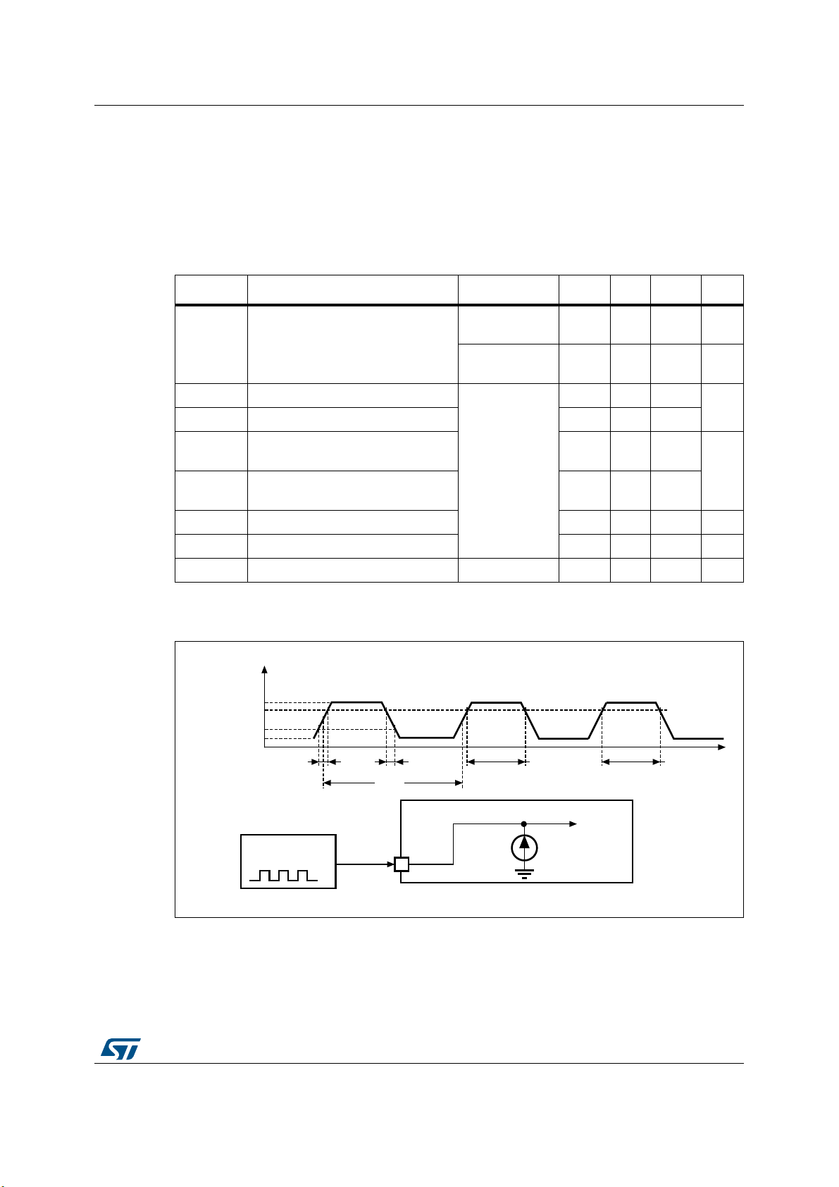
STM32L052x6 STM32L052x8 Electrical characteristics
ai18232c
OS C _I N
EXTERNAL
STM32Lxx
CLOCK SOURC E
V
HSEH
t
f(HSE)
t
W(HSE)
I
L
90%
10%
T
HSE
t
t
r(HSE)
t
W(HSE)
f
HSE_ext
V
HSEL
6.3.6 External clock source characteristics
High-speed external user clock generated from an external source
In bypass mode the HSE oscillator is switched off and the input pin is a standard GPIO.The
external clock signal has to respect the I/O characteristics in Section 6.3.12. However, the
recommended clock input waveform is shown in Figure 19.
Table 42. High-speed external user clock characteristics
Symbol Parameter Conditions Min Typ Max Unit
(1)
f
HSE_ext
V
HSEH
V
HSEL
t
w(HSE)
t
w(HSE)
t
r(HSE)
t
f(HSE)
C
in(HSE)
DuCy
I
User external clock source
frequency
OSC_IN input pin high level voltage
OSC_IN input pin low level voltage V
OSC_IN high or low time 12 - -
OSC_IN rise or fall time - - 20
OSC_IN input capacitance - 2.6 - pF
Duty cycle 45 - 55 %
(HSE)
OSC_IN Input leakage current V
L
1. Guaranteed by design.
Figure 19. High-speed external clock source AC timing diagram
CSS is ON or
PLL is used
CSS is OFF,
PLL not used
-
≤ V
IN
≤ V
DD
SS
1832MHz
0832MHz
0.7V
SS
DD
-V
-0.3V
DD
DD
V
ns
--±1µA
DS10182 Rev 9 75/150
114
Page 76

Electrical characteristics STM32L052x6 STM32L052x8
ai18233c
OS C3 2_ IN
EXTERNAL
STM32Lxx
CLOCK SOURC E
V
LSEH
t
f(LSE)
t
W(LSE)
I
L
90%
10%
T
LSE
t
t
r(LSE)
t
W(LSE)
f
LSE_ext
V
LSEL
Low-speed external user clock generated from an external source
The characteristics given in the following table result from tests performed using a lowspeed external clock source, and under ambient temperature and supply voltage conditions
summarized in Table 25.
Table 43. Low-speed external user clock characteristics
Symbol Parameter Conditions Min Typ Max Unit
(1)
f
LSE_ext
V
LSEH
V
t
w(LSE)
t
w(LSE)
t
r(LSE)
t
f(LSE)
C
IN(LSE)
DuCy
LSEL
I
User external clock source
frequency
OSC32_IN input pin high level
voltage
OSC32_IN input pin low level
voltage
OSC32_IN high or low time 465 - -
OSC32_IN rise or fall time - - 10
OSC32_IN input capacitance - - 0.6 - pF
Duty cycle - 45 - 55 %
(LSE)
OSC32_IN Input leakage current V
L
1. Guaranteed by design, not tested in production
Figure 20. Low-speed external clock source AC timing diagram
SS
≤ V
-
IN
≤ V
DD
1 32.768 1000 kHz
0.7V
DD
-V
DD
V
V
SS
-0.3V
DD
ns
--±1µA
76/150 DS10182 Rev 9
Page 77

STM32L052x6 STM32L052x8 Electrical characteristics
High-speed external clock generated from a crystal/ceramic resonator
The high-speed external (HSE) clock can be supplied with a 1 to 25 MHz crystal/ceramic
resonator oscillator. All the information given in this paragraph are based on
characterization results obtained with typical external components specified in Table 44. In
the application, the resonator and the load capacitors have to be placed as close as
possible to the oscillator pins in order to minimize output distortion and startup stabilization
time. Refer to the crystal resonator manufacturer for more details on the resonator
characteristics (frequency, package, accuracy).
Table 44. HSE oscillator characteristics
Symbol Parameter Conditions Min Typ Max Unit
(1)
f
OSC_IN
t
SU(HSE)
Oscillator frequency - 1 25 MHz
Feedback resistor - - 200 - kΩ
R
F
Maximum critical crystal
G
m
transconductance
Startup time VDD is stabilized - 2 - ms
(2)
Startup - - 700
µA
/V
1. Guaranteed by design.
2. Guaranteed by characterization results. t
enabled (by software) to a stabilized 8 MHz oscillation is reached. This value is measured for a standard
crystal resonator and it can vary significantly with the crystal manufacturer.
is the startup time measured from the moment it is
SU(HSE)
For CL1 and CL2, it is recommended to use high-quality external ceramic capacitors in the
5 pF to 25 pF range (typ.), designed for high-frequency applications, and selected to match
the requirements of the crystal or resonator (see Figure 21). C
and C
L1
are usually the
L2
same size. The crystal manufacturer typically specifies a load capacitance which is the
series combination of C
and CL2. PCB and MCU pin capacitance must be included (10 pF
L1
can be used as a rough estimate of the combined pin and board capacitance) when sizing
C
and CL2. Refer to the application note AN2867 “Oscillator design guide for ST
L1
microcontrollers” available from the ST website www.st.com.
Figure 21. HSE oscillator circuit diagram
f
to core
R
m
L
m
C
m
Resonator
R
C
O
C
L1
OSC_IN
Resonator
F
g
m
HSE
Consumption
control
C
L2
OSC_OUT
STM32
ai18235b
DS10182 Rev 9 77/150
114
Page 78

Electrical characteristics STM32L052x6 STM32L052x8
MS30253V2
OSC32_IN
OSC32_OUT
Drive
programmable
amplifier
f
LSE
32.768 kHz
resonator
Resonator with integrated
capacitors
C
L1
C
L2
Low-speed external clock generated from a crystal/ceramic resonator
The low-speed external (LSE) clock can be supplied with a 32.768 kHz crystal/ceramic
resonator oscillator. All the information given in this paragraph are based on
characterization results obtained with typical external components specified in Table 45. In
the application, the resonator and the load capacitors have to be placed as close as
possible to the oscillator pins in order to minimize output distortion and startup stabilization
time. Refer to the crystal resonator manufacturer for more details on the resonator
characteristics (frequency, package, accuracy).
Table 45. LSE oscillator characteristics
Symbol Parameter Conditions
(2)
(1)
(2)
Min
Typ Ma x Uni t
f
LSE
G
t
SU(LSE)
1. Guaranteed by design.
2. Refer to the note and caution paragraphs below the table, and to the application note AN2867 “Oscillator design guide for
ST microcontrollers”.
3. Guaranteed by characterization results. t
to a stabilized 32.768 kHz oscillation is reached. This value is measured for a standard crystal resonator and it can vary
significantly with the crystal manufacturer. To increase speed, address a lower-drive quartz with a high- driver mode.
LSE oscillator frequency - 32.768 - kHz
LSEDRV[1:0]=00
lower driving capability
LSEDRV[1:0]= 01
Maximum critical crystal
m
transconductance
medium low driving capability
LSEDRV[1:0] = 10
medium high driving capability
LSEDRV[1:0]=11
higher driving capability
(3)
Startup time VDD is stabilized - 2 - s
is the startup time measured from the moment it is enabled (by software)
SU(LSE)
--0.5
- - 0.75
--1.7
--2.7
Note: For information on selecting the crystal, refer to the application note AN2867 “Oscillator
design guide for ST microcontrollers” available from the ST website www.st.com.
Figure 22. Typical application with a 32.768 kHz crystal
µA/V
Note: An external resistor is not required between OSC32_IN and OSC32_OUT and it is forbidden
78/150 DS10182 Rev 9
to add one.
Page 79

STM32L052x6 STM32L052x8 Electrical characteristics
MSv34791V1
-6.00%
-5.00%
-4.00%
-3.00%
-2.00%
-1.00%
0.00%
1.00%
2.00%
3.00%
4.00%
-60 -40 -20 0 20 40 60 80 100 120 140
1.65V min
3V typ
3.6V max
1.65V max
3.6V min
6.3.7 Internal clock source characteristics
The parameters given in Table 46 are derived from tests performed under ambient
temperature and V
High-speed internal 16 MHz (HSI16) RC oscillator
Symbol Parameter Conditions Min Typ Max Unit
supply voltage conditions summarized in Table 25.
DD
Table 46. 16 MHz HSI16 oscillator characteristics
f
HSI16
TRIM
ACC
HSI16
(2)
t
SU(HSI16)
I
DD(HSI16)
1. The trimming step differs depending on the trimming code. It is usually negative on the codes which are
multiples of 16 (0x00, 0x10, 0x20, 0x30...0xE0).
2. Guaranteed by characterization results.
3. Guaranteed by test in production.
Frequency VDD = 3.0 V - 16 - MHz
HSI16 user-
(1)(2)
trimmed resolution
Accuracy of the
factory-calibrated
HSI16 oscillator
HSI16 oscillator
(2)
startup time
HSI16 oscillator
(2)
power consumption
Trimming code is not a multiple of 16 - ± 0.4 0.7 %
Trimming code is a multiple of 16 - - ± 1.5 %
= 3.0 V, TA = 25 °C -1
V
DDA
= 3.0 V, TA = 0 to 55 °C -1.5 - 1.5 %
V
DDA
= 3.0 V, TA = -10 to 70 °C -2 - 2 %
V
DDA
V
= 3.0 V, TA = -10 to 85 °C -2.5 - 2 %
DDA
= 3.0 V, TA = -10 to 105 °C -4 - 2 %
V
DDA
V
= 1.65 V to 3.6 V
DDA
TA = − 40 to 125 °C
(3)
-1
-5.45 - 3.25 %
- - 3.7 6 µs
- - 100 140 µA
(3)
Figure 23. HSI16 minimum and maximum value versus temperature
%
DS10182 Rev 9 79/150
114
Page 80

Electrical characteristics STM32L052x6 STM32L052x8
High-speed internal 48 MHz (HSI48) RC oscillator
Table 47. HSI48 oscillator characteristics
Symbol Parameter Conditions Min Typ Max Unit
(1)
f
HSI48
TRIM HSI48 user-trimming step 0.09
DuCy
(HSI48)
ACC
HSI48
Frequency - 48 - MHz
Duty cycle 45
Accuracy of the HSI48
oscillator (factory calibrated
TA = 25 °C -4
(2)
(2)
(3)
0.14 0.2
-55
-4
(2)
(2)
(3)
before CRS calibration)
t
su(HSI48)
I
DDA(HSI48)
1. V
DDA
2. Guaranteed by design.
3. Guaranteed by characterization results.
HSI48 oscillator startup time - - 6
HSI48 oscillator power
consumption
= 3.3 V, TA = –40 to 125 °C unless otherwise specified.
- 330 380
(2)
(2)
Low-speed internal (LSI) RC oscillator
Symbol Parameter Min Typ Max Unit
(1)
f
LSI
D
LSI
t
su(LSI)
I
DD(LSI)
1. Guaranteed by test in production.
2. This is a deviation for an individual part, once the initial frequency has been measured.
3. Guaranteed by design.
LSI frequency 26 38 56 kHz
LSI oscillator frequency drift
(2)
0°C ≤ TA ≤ 85°C
(3)
LSI oscillator startup time - - 200 µs
(3)
LSI oscillator power consumption - 400 510 nA
Table 48. LSI oscillator characteristics
-10 - 4 %
%
%
%
µs
µA
Multi-speed internal (MSI) RC oscillator
Symbol Parameter Condition Typ Max Unit
f
MSI
Frequency after factory calibration, done at
= 3.3 V and TA = 25 °C
V
DD
80/150 DS10182 Rev 9
Table 49. MSI oscillator characteristics
MSI range 0 65.5 -
MSI range 1 131 -
kHz
MSI range 2 262 -
MSI range 3 524 -
MSI range 4 1.05 -
MHzMSI range 5 2.1 -
MSI range 6 4.2 -
Page 81

STM32L052x6 STM32L052x8 Electrical characteristics
Table 49. MSI oscillator characteristics (continued)
Symbol Parameter Condition Typ Max Unit
ACC
D
TEMP(MSI)
D
VOLT(MSI)
I
DD(MSI)
Frequency error after factory calibration - ±0.5 - %
MSI
MSI oscillator frequency drift
0 °C ≤ TA ≤ 85 °C
- ±3-
MSI range 0 − 8.9 +7.0
MSI range 1 − 7.1 +5.0
(1)
MSI oscillator frequency drift
= 3.3 V, − 40 °C ≤ TA ≤ 110 °C
V
DD
MSI range 2 − 6.4 +4.0
MSI range 3 − 6.2 +3.0
MSI range 4 − 5.2 +3.0
MSI range 5 − 4.8 +2.0
MSI range 6 − 4.7 +2.0
MSI oscillator frequency drift
(1)
1.65 V ≤ VDD ≤ 3.6 V, TA = 25 °C
--2.5%/V
MSI range 0 0.75 -
MSI range 1 1 -
MSI range 2 1.5 -
(2)
MSI oscillator power consumption
MSI range 3 2.5 -
MSI range 4 4.5 -
MSI range 5 8 -
%
µA
t
SU(MSI)
MSI oscillator startup time
MSI range 6 15 -
MSI range 0 30 -
MSI range 1 20 -
MSI range 2 15 -
MSI range 3 10 -
MSI range 4 6 -
MSI range 5 5 -
MSI range 6,
Voltage range 1
3.5 -
and 2
MSI range 6,
Voltage range 3
5-
µs
DS10182 Rev 9 81/150
114
Page 82
Electrical characteristics STM32L052x6 STM32L052x8
Table 49. MSI oscillator characteristics (continued)
Symbol Parameter Condition Typ Max Unit
MSI range 0 - 40
MSI range 1 - 20
MSI range 2 - 10
MSI range 3 - 4
t
STAB(MSI)
f
OVER(MSI)
1. This is a deviation for an individual part, once the initial frequency has been measured.
2. Guaranteed by characterization results.
(2)
MSI oscillator stabilization time
MSI oscillator frequency overshoot
6.3.8 PLL characteristics
The parameters given in Table 50 are derived from tests performed under ambient
temperature and V
Symbol Parameter
f
PLL_IN
supply voltage conditions summarized in Table 25.
DD
PLL input clock
PLL input clock duty cycle 45 - 55 %
MSI range 4 - 2.5
MSI range 5 - 2
MSI range 6,
Voltage range 1
and 2
MSI range 3,
Voltage range 3
Any range to
range 5
Any range to
range 6
Table 50. PLL characteristics
Min Typ Max
(2)
2- 24MHz
Value
µs
-2
-3
-4
MHz
-6
(1)
Unit
f
PLL_OUT
t
LOCK
PLL output clock 2 - 32 MHz
PLL input = 16 MHz
PLL VCO = 96 MHz
Jitter Cycle-to-cycle jitter - ±
(PLL) Current consumption on V
I
DDA
(PLL) Current consumption on V
I
DD
1. Guaranteed by characterization results.
2. Take care of using the appropriate multiplier factors so as to have PLL input clock values compatible with
the range defined by f
PLL_OUT
.
DDA
DD
82/150 DS10182 Rev 9
- 115 160 µs
600 ps
- 220 450
µA
- 120 150
Page 83

STM32L052x6 STM32L052x8 Electrical characteristics
6.3.9 Memory characteristics
RAM memory
Symbol Parameter Conditions Min Typ Max Unit
VRM Data retention mode
1. Minimum supply voltage without losing data stored in RAM (in Stop mode or under Reset) or in hardware
registers (only in Stop mode).
Flash memory and data EEPROM
Table 51. RAM and hardware registers
(1)
STOP mode (or RESET) 1.65 - - V
Table 52. Flash memory and data EEPROM characteristics
Symbol Parameter Conditions Min Typ Max
V
t
Operating voltage
DD
Read / Write / Erase
Programming time for
prog
word or half-page
-1.65-3.6V
Erasing - 3.28 3.94
Programming - 3.28 3.94
Average current during
the whole programming /
- 500 700 µA
erase operation
I
DD
Maximum current (peak)
during the whole
programming / erase
TA = 25 °C, VDD = 3.6 V
-1.52.5mA
operation
1. Guaranteed by design.
Table 53. Flash memory and data EEPROM endurance and retention
Val ue
Symbol Parameter Conditions
Min
N
CYC
Cycling (erase / write)
Program memory
Cycling (erase / write)
EEPROM data memory
(2)
Cycling (erase / write)
Program memory
Cycling (erase / write)
= -40°C to 105 °C
T
A
T
= -40°C to 125 °C
A
10
100
0.2
EEPROM data memory
(1)
Unit
ms
Unit
(1)
kcycles
2
DS10182 Rev 9 83/150
114
Page 84

Electrical characteristics STM32L052x6 STM32L052x8
Table 53. Flash memory and data EEPROM endurance and retention (continued)
Val ue
Symbol Parameter Conditions
Min
(1)
Unit
Data retention (program memory) after
10 kcycles at T
A
Data retention (EEPROM data memory)
after 100 kcycles at T
Data retention (program memory) after
t
RET
10 kcycles at T
(2)
Data retention (EEPROM data memory)
A
after 100 kcycles at T
Data retention (program memory) after
200 cycles at T
A
Data retention (EEPROM data memory)
after 2 kcycles at T
1. Guaranteed by characterization results.
2. Characterization is done according to JEDEC JESD22-A117.
6.3.10 EMC characteristics
Susceptibility tests are performed on a sample basis during device characterization.
Functional EMS (electromagnetic susceptibility)
While a simple application is executed on the device (toggling 2 LEDs through I/O ports).
the device is stressed by two electromagnetic events until a failure occurs. The failure is
indicated by the LEDs:
• Electrostatic discharge (ESD) (positive and negative) is applied to all device pins until
a functional disturbance occurs. This test is compliant with the IEC 61000-4-2 standard.
• FTB: A Burst of Fast Transient voltage (positive and negative) is applied to V
V
through a 100 pF capacitor, until a functional disturbance occurs. This test is
SS
compliant with the IEC 61000-4-4 standard.
= 85 °C
= 85 °C
A
= 105 °C
= 105 °C
A
= 125 °C
= 125 °C
A
T
T
T
RET
RET
RET
= +85 °C
= +105 °C
= +125 °C
30
30
10
DD
years
and
A device reset allows normal operations to be resumed.
The test results are given in Table 54. They are based on the EMS levels and classes
defined in application note AN1709.
Symbol Parameter Conditions
V
FESD
Voltage limits to be applied on any I/O pin to
induce a functional disturbance
Fast transient voltage burst limits to be
V
EFTB
applied through 100 pF on V
pins to induce a functional disturbance
84/150 DS10182 Rev 9
Table 54. EMS characteristics
and V
DD
SS
= 3.3 V, LQFP64, TA = +25 °C,
V
DD
= 32 MHz
f
HCLK
conforms to IEC 61000-4-2
V
= 3.3 V, LQFP64, TA = +25 °C,
DD
= 32 MHz
f
HCLK
conforms to IEC 61000-4-4
Level/
Class
3B
4A
Page 85

STM32L052x6 STM32L052x8 Electrical characteristics
Designing hardened software to avoid noise problems
EMC characterization and optimization are performed at component level with a typical
application environment and simplified MCU software. It should be noted that good EMC
performance is highly dependent on the user application and the software in particular.
Therefore it is recommended that the user applies EMC software optimization and
prequalification tests in relation with the EMC level requested for his application.
Software recommendations
The software flowchart must include the management of runaway conditions such as:
• Corrupted program counter
• Unexpected reset
• Critical data corruption (control registers...)
Prequalification trials
Most of the common failures (unexpected reset and program counter corruption) can be
reproduced by manually forcing a low state on the NRST pin or the oscillator pins for 1
second.
To complete these trials, ESD stress can be applied directly on the device, over the range of
specification values. When unexpected behavior is detected, the software can be hardened
to prevent unrecoverable errors occurring (see application note AN1015).
Electromagnetic Interference (EMI)
The electromagnetic field emitted by the device are monitored while a simple application is
executed (toggling 2 LEDs through the I/O ports). This emission test is compliant with
IEC 61967-2 standard which specifies the test board and the pin loading.
Symbol Parameter Conditions
V
DD
EMI
Peak level
S
TA = 25 °C,
compliant with IEC
61967-2
Table 55. EMI characteristics
Monitored
frequency band
0.1 to 30 MHz -21 -15 -12
= 3.6 V,
130 MHz to 1GHz -10 -11 -7
EMI Level 1 1 1 -
Max vs. f
8 MHz/
4 MHz
osc/fCPU
8 MHz/
16 MHz
8 MHz/
32 MHz
Unit
dBµV30 to 130 MHz -14 -12 -1
DS10182 Rev 9 85/150
114
Page 86

Electrical characteristics STM32L052x6 STM32L052x8
6.3.11 Electrical sensitivity characteristics
Based on three different tests (ESD, LU) using specific measurement methods, the device is
stressed in order to determine its performance in terms of electrical sensitivity.
Electrostatic discharge (ESD)
Electrostatic discharges (a positive then a negative pulse separated by 1 second) are
applied to the pins of each sample according to each pin combination. The sample size
depends on the number of supply pins in the device (3 parts × (n+1) supply pins). This test
conforms to the ANSI/JEDEC standard.
Table 56. ESD absolute maximum ratings
Symbol Ratings Conditions Class
= +25 °C,
T
V
ESD(HBM)
Electrostatic discharge
voltage (human body model)
Electrostatic discharge
V
ESD(CDM)
voltage (charge device
model)
1. Guaranteed by characterization results.
A
conforming to
ANSI/JEDEC JS-001
TA = +25 °C,
conforming to
ANSI/ESD STM5.3.1.
22000
C4 500
Maximum
(1)
value
Static latch-up
Two complementary static tests are required on six parts to assess the latch-up
performance:
• A supply overvoltage is applied to each power supply pin
• A current injection is applied to each input, output and configurable I/O pin
These tests are compliant with EIA/JESD 78A IC latch-up standard.
Symbol Parameter Conditions Class
LU Static latch-up class T
Table 57. Electrical sensitivities
= +125 °C conforming to JESD78A II level A
A
Unit
V
86/150 DS10182 Rev 9
Page 87

STM32L052x6 STM32L052x8 Electrical characteristics
6.3.12 I/O current injection characteristics
As a general rule, current injection to the I/O pins, due to external voltage below VSS or
above V
However, in order to give an indication of the robustness of the microcontroller in cases
when abnormal injection accidentally happens, susceptibility tests are performed on a
sample basis during device characterization.
Functional susceptibility to I/O current injection
While a simple application is executed on the device, the device is stressed by injecting
current into the I/O pins programmed in floating input mode. While current is injected into
the I/O pin, one at a time, the device is checked for functional failures.
The failure is indicated by an out of range parameter: ADC error above a certain limit (higher
than 5 LSB TUE), out of conventional limits of induced leakage current on adjacent pins (out
of –5 µA/+0 µA range), or other functional failure (for example reset occurrence oscillator
frequency deviation).
The test results are given in the Table 58.
Symbol Description
I
INJ
(for standard pins) should be avoided during normal product operation.
DD
Table 58. I/O current injection susceptibility
Functional susceptibility
Negative
injection
Injected current on BOOT0 -0 NA
Injected current on PA0, PA4, PA5, PA11,
PA12, PC15, PH0 and PH1
Injected current on any other FT, FTf pins -5
Injected current on any other pins -5
-5 0
(2)
(2)
Positive
injection
(1)
(1)
NA
+5
Unit
mA
1. Current injection is not possible.
2. It is recommended to add a Schottky diode (pin to ground) to analog pins which may potentially inject
negative currents.
DS10182 Rev 9 87/150
114
Page 88

Electrical characteristics STM32L052x6 STM32L052x8
6.3.13 I/O port characteristics
General input/output characteristics
Unless otherwise specified, the parameters given in Table 59 are derived from tests
performed under the conditions summarized in Table 25. All I/Os are CMOS and TTL
compliant.
Table 59. I/O static characteristics
Symbol Parameter Conditions Min Typ
Max Unit
Input low level voltage
V
IL
TC, FT, FTf, RST
I/Os
- - 0.3V
BOOT0 pin - - 0.14V
V
Input high level voltage All I/Os 0.7 V
IH
V
I/O Schmitt trigger voltage hysteresis
(2)
hys
Standard I/Os - 10% V
BOOT0 pin - 0.01 -
V
≤ V
IN
≤ V
DD
SS
All I/Os except for
PA11, PA1 2, BOOT 0
DD
--±50
--
(3)
DD
and FTf I/Os
≤ V
≤ V
SS
FTf I/Os
≤ V
DD
IN
IN
IN
≤ V
≤ V
≤ 5 V
DD,
DD
- - -50/+250
- - ±100
- - 200
Input leakage current
I
lkg
(4)
V
SS
PA11 and PA12 I/Os
V
V
All I/Os except for
PA11, PA1 2, BOOT 0
and FTf I/Os
≤ V
DD
FTf I/Os
≤ V
DD
IN
IN
≤ 5 V
≤ 5 V
- - 500
--10µA
V
V
PA11, PA12 and
BOOT0
R
R
1. Guaranteed by characterization.
2. Hysteresis voltage between Schmitt trigger switching levels. Guaranteed by characterization results.
3. With a minimum of 200 mV. Guaranteed by characterization results.
4. The max. value may be exceeded if negative current is injected on adjacent pins.
5. Pull-up and pull-down resistors are designed with a true resistance in series with a switchable PMOS/NMOS. This
Weak pull-up equivalent resistor
PU
Weak pull-down equivalent resistor
PD
I/O pin capacitance - - 5 - pF
C
IO
MOS/NMOS contribution to the series resistance is minimum (~10% order).
(5)
(5)
V
= V
IN
SS
V
= V
IN
DD
25 45 65 kΩ
25 45 65 kΩ
DD
(1)
DD
V
-
nA
nA
88/150 DS10182 Rev 9
Page 89

STM32L052x6 STM32L052x8 Electrical characteristics
MSv34789V1
V
DD
(V)
V
IHmin
2.0
V
ILmax
0.7
V
IL
/V
IH
(V)
1.3
2.0 3.6
CMOS standard requirements V
IHmin
= 0.7V
DD
V
ILmax
= 0.3V
DD
0.6
2.7 3.0 3.3
CMOS standard requirements V
ILmax
= 0.3V
DD
V
IHmin
= 0.39V
DD
+0.59 (all pins
except BOOT0, PC15, PH0/1
V
IHmin
= 0.45V
DD
+0.38 for
BOOT0, PC15, PH0/1
Input range not
guaranteed
MSv34790V1
V
DD
(V)
V
IHmin
2.0
V
ILmax
0.8
V
IL
/V
IH
(V)
1.3
2.0 3.6
TTL standard requirements V
IHmin
= 2 V
V
ILmax
= 0.3V
DD
0.7
2.7 3.0 3.3
TTL standard requirements V
ILmax
= 0.8 V
Input range not
guaranteed
V
IHmin
= 0.39V
DD
+0.59 (all pins
except BOOT0, PC15, PH0/1
V
IHmin
= 0.45V
DD
+0.38 for
BOOT0, PC15, PH0/1
Figure 24. VIH/VIL versus VDD (CMOS I/Os)
Figure 25. V
versus VDD (TTL I/Os)
IH/VIL
Output driving current
The GPIOs (general purpose input/outputs) can sink or source up to ±8 mA, and sink or
source up to ±15 mA with the non-standard V
OL/VOH
In the user application, the number of I/O pins which can drive current must be limited to
respect the absolute maximum rating specified in Section 6.2:
• The sum of the currents sourced by all the I/Os on V
consumption of the MCU sourced on V
I
(see Table 23).
VDD(Σ)
DD,
• The sum of the currents sunk by all the I/Os on V
consumption of the MCU sunk on V
I
(see Table 23).
VSS(Σ)
cannot exceed the absolute maximum rating
SS
specifications given in Table 60.
plus the maximum Run
DD,
cannot exceed the absolute maximum rating
plus the maximum Run
SS
DS10182 Rev 9 89/150
114
Page 90

Electrical characteristics STM32L052x6 STM32L052x8
Output voltage levels
Unless otherwise specified, the parameters given in Table 60 are derived from tests
performed under ambient temperature and V
Table 25. All I/Os are CMOS and TTL compliant.
Symbol Parameter Conditions Min Max Unit
Output low level voltage for an I/O
(1)
V
OL
V
OH
V
OL
(3)(4)
V
OH
(1)(4)
V
OL
(3)(4)
V
OH
pin
Output high level voltage for an I/O
(3)
pin
Output low level voltage for an I/O
(1)
pin
Output high level voltage for an I/O
pin
Output low level voltage for an I/O
pin
Output high level voltage for an I/O
pin
Table 60. Output voltage characteristics
supply voltage conditions summarized in
DD
= +8 mA
(2)
,
CMOS port
I
IO
2.7 V ≤ VDD ≤ 3.6 V
(2)
DD
DD
DD
,
≤ 3.6 V
(2)
,
≤ 3.6 V
≤ 3.6 V
TTL port
I
2.7 V
TTL port
I
2.7 V
I
IO
2.7 V
I
IO
=+ 8 mA
IO
≤ V
= -6 mA
IO
≤ V
= +15 mA
≤ V
= -15 mA
2.7 V ≤ VDD ≤ 3.6 V
-0.4
-0.4 -
V
DD
-0.4
2.4 -
-1.3
V
-1.3 -
DD
V
(1)(4)
V
OL
(3)(4)
V
OH
V
OLFM+
1. The IIO current sunk by the device must always respect the absolute maximum rating specified in Table 23.
The sum of the currents sunk by all the I/Os (I/O ports and control pins) must always be respected and
must not exceed ΣI
2. TTL and CMOS outputs are compatible with JEDEC standards JESD36 and JESD52.
3. The IIO current sourced by the device must always respect the absolute maximum rating specified in
Table 23. The sum of the currents sourced by all the I/Os (I/O ports and control pins) must always be
respected and must not exceed ΣI
4. Guaranteed by characterization results.
Output low level voltage for an I/O
pin
Output high level voltage for an I/O
pin
Output low level voltage for an FTf
(1)(4)
I/O pin in Fm+ mode
.
IO(PIN)
IO(PIN)
.
I
= +4 mA
IO
1.65 V ≤ VDD < 3.6 V
I
= -4 mA
IO
≤ V
= 20 mA
IO
≤ 3.6 V
DD
1.65 V
I
2.7 V ≤ VDD ≤ 3.6 V
I
= 10 mA
IO
1.65 V ≤ VDD ≤ 3.6 V
-0.45
-0.45 -
V
DD
-0.4
-0.4
90/150 DS10182 Rev 9
Page 91

STM32L052x6 STM32L052x8 Electrical characteristics
Input/output AC characteristics
The definition and values of input/output AC characteristics are given in Figure 26 and
Table 61, respectively.
Unless otherwise specified, the parameters given in Table 61 are derived from tests
performed under ambient temperature and V
Table 25.
Table 61. I/O AC characteristics
supply voltage conditions summarized in
DD
(1)
OSPEEDRx[1:0]
bit value
(1)
00
01
10
11
Fm+
configuration
(4)
-t
Symbol Parameter Conditions Min Max
f
max(IO)out
t
f(IO)out
t
r(IO)out
f
max(IO)out
t
f(IO)out
t
r(IO)out
F
max(IO)out
t
f(IO)out
t
r(IO)out
F
max(IO)out
t
f(IO)out
t
r(IO)out
f
max(IO)out
t
f(IO)out
t
r(IO)out
f
max(IO)out
t
f(IO)out
t
r(IO)out
CL = 50 pF, V
Maximum frequency
(3)
= 50 pF, V
C
L
CL = 50 pF, V
Output rise and fall time
= 50 pF, V
C
L
CL = 50 pF, V
Maximum frequency
Output rise and fall time
Maximum frequency
(3)
(3)
= 50 pF, V
C
L
C
= 50 pF, V
L
= 50 pF, V
C
L
CL = 50 pF, V
= 50 pF, V
C
L
CL = 50 pF, V
Output rise and fall time
= 50 pF, V
C
L
CL = 30 pF, V
Maximum frequency
Output rise and fall time
Maximum frequency
Output fall time - 10
(3)
(3)
= 50 pF, V
C
L
C
= 30 pF, V
L
= 50 pF, V
C
L
CL = 50 pF, V
Output rise time - 30
Maximum frequency
Output fall time - 15
(3)
CL = 50 pF, V
Output rise time - 60
= 2.7 V to 3.6 V - 400
DD
= 1.65 V to 2.7 V - 100
DD
= 2.7 V to 3.6 V - 125
DD
= 1.65 V to 2.7 V - 320
DD
= 2.7 V to 3.6 V - 2
DD
= 1.65 V to 2.7 V - 0.6
DD
= 2.7 V to 3.6 V - 30
DD
= 1.65 V to 2.7 V - 65
DD
= 2.7 V to 3.6 V - 10
DD
= 1.65 V to 2.7 V - 2
DD
= 2.7 V to 3.6 V - 13
DD
= 1.65 V to 2.7 V - 28
DD
= 2.7 V to 3.6 V - 35
DD
= 1.65 V to 2.7 V - 10
DD
= 2.7 V to 3.6 V - 6
DD
= 1.65 V to 2.7 V - 17
DD
-1MHz
= 2.5 V to 3.6 V
DD
-350KHz
= 1.65 V to 3.6 V
DD
Pulse width of external
EXTIpw
signals detected by the
-8-ns
EXTI controller
(2)
Unit
kHz
ns
MHz
ns
MHz
ns
MHz
ns
ns
ns
1. The I/O speed is configured using the OSPEEDRx[1:0] bits. Refer to the line reference manual for a description of GPIO Port
configuration register.
2. Guaranteed by design.
3. The maximum frequency is defined in Figure 26.
4. When Fm+ configuration is set, the I/O speed control is bypassed. Refer to the line reference manual for a detailed
description of Fm+ I/O configuration.
DS10182 Rev 9 91/150
114
Page 92

Electrical characteristics STM32L052x6 STM32L052x8
ai14131d
10%
90%
50%
t
r(IO)out
OUTPUT
EXTERNAL
ON CL
Maximum frequency is achieved if (tr + tf) ≤ (2/3)T and if the duty cycle is (45-55%)
when loaded by C
L specified in the table “ I/O AC characteristics”.
10%
50%
90%
T
t
f(IO)out
Figure 26. I/O AC characteristics definition
6.3.14 NRST pin characteristics
The NRST pin input driver uses CMOS technology. It is connected to a permanent pull-up
resistor, R
Unless otherwise specified, the parameters given in Table 62 are derived from tests
performed under ambient temperature and V
Table 25.
, except when it is internally driven low (see Table 62).
PU
supply voltage conditions summarized in
DD
Table 62. NRST pin characteristics
Symbol Parameter Conditions Min Typ Max Unit
V
IL(NRST)
V
IH(NRST)
V
OL(NRST)
V
hys(NRST)
V
F(NRST)
V
NF(NRST)
1. Guaranteed by design.
2. 200 mV minimum value
3. The pull-up is designed with a true resistance in series with a switchable PMOS. This PMOS contribution to
(1)
NRST input low level voltage - V
(1)
NRST input high level voltage - 1.4 - V
NRST output low level
(1)
voltage
NRST Schmitt trigger voltage
(1)
hysteresis
R
PU
the series resistance is around 10%.
Weak pull-up equivalent
(3)
resistor
(1)
NRST input filtered pulse - - - 50 ns
(1)
NRST input not filtered pulse - 350 - - ns
= 2 mA
I
OL
2.7 V < VDD < 3.6 V
= 1.5 mA
I
OL
1.65 V < V
< 2.7 V
DD
--10%V
V
= V
IN
SS
SS
-0.8
DD
--
0.4
--
(2)
DD
-mV
25 45 65 kΩ
V
92/150 DS10182 Rev 9
Page 93

STM32L052x6 STM32L052x8 Electrical characteristics
069
5
38
9
''
,QWHUQDOUHVHW
([WHUQDO
UHVHWFLUFXLW
1567
)LOWHU
)
Figure 27. Recommended NRST pin protection
1. The reset network protects the device against parasitic resets.
2. The external capacitor must be placed as close as possible to the device.
3. The user must ensure that the level on the NRST pin can go below the V
Table 62. Otherwise the reset will not be taken into account by the device.
max level specified in
IL(NRST)
6.3.15 12-bit ADC characteristics
Unless otherwise specified, the parameters given in Table 63 are derived from tests
performed under ambient temperature, f
summarized in Table 25: General operating conditions.
frequency and V
PCLK
supply voltage conditions
DDA
Note: It is recommended to perform a calibration after each power-up.
Symbol Parameter Conditions Min Typ
V
DDA
Analog supply voltage for
ADC ON
Current consumption of the
I
DDA (ADC)
f
ADC
(3)
f
S
(3)
f
TRIG
V
AIN
(3)
R
AIN
ADC on V
Current consumption of the
ADC on V
ADC clock frequency
Sampling rate 12-bit resolution 0.01 - 1.14 MHz
External trigger frequency
Conversion voltage range - 0 - V
External input impedance
DDA
DD
and V
(2)
Table 63. ADC characteristics
Fast channel 1.65 - 3.6
Standard channel 1.75
1.14 Msps - 200 -
REF+
Voltage scaling Range 1 0.14 - 16
Voltage scaling Range 3 0.14 - 4
10 ksps - 40 -
1.14 Msps - 70 -
10 ksps - 1 -
= 16 MHz,
f
ADC
12-bit resolution
---171/f
See Equation 1 and
Table 64 for details
Max Unit
(1)
-3.6
V
µA
MHzVoltage scaling Range 2 0.14 - 8
- - 941 kHz
ADC
--50kΩ
DS10182 Rev 9 93/150
114
Page 94

Electrical characteristics STM32L052x6 STM32L052x8
Table 63. ADC characteristics (continued)
Symbol Parameter Conditions Min Typ
(3)(4)
R
ADC
C
t
CAL
ADC
(3)(5)
Sampling switch resistance - - - 1 kΩ
Internal sample and hold
(3)
capacitor
Calibration time
---8pF
f
= 16 MHz 5.2 µs
ADC
-831/f
1.5 ADC
W
LATENCY
ADC_DR register write
(6)
latency
ADC clock = HSI16
ADC clock = PCLK/2 - 4.5 -
cycles + 2
f
cycles
PCLK
ADC clock = PCLK/4 - 8.5 -
t
latr
Jitter
(3)
Trigger conversion latency
ADC jitter on trigger
ADC
conversion
f
ADC
f
f
= f
ADC
ADC
/2 = 16 MHz 0.266 µs
PCLK
f
ADC
= f
f
ADC
= f
f
= f
PCLK
= f
HSI16
ADC
/2 8.5 1/f
PCLK
/4 = 8 MHz 0.516 µs
/4 16.5 1/f
PCLK
= 16 MHz 0.252 - 0.260 µs
= f
HSI16
-1-1/f
-
Max Unit
1.5 ADC
cycles + 3
cycles
f
PCLK
ADC
-
f
PCLK
cycle
f
PCLK
cycle
PCLK
PCLK
HSI16
f
= 16 MHz 0.093 - 10.03 µs
(3)
t
S
t
UP_LDO
(3)(5)
t
STAB
t
ConV
1. V
DDA
2. A current consumption proportional to the APB clock frequency has to be added (see Table 39: Peripheral current
consumption in Run or Sleep mode).
3. Guaranteed by design.
4. Standard channels have an extra protection resistance which depends on supply voltage. Refer to Table 64: R
f
= 16 MHz.
ADC
5. This parameter only includes the ADC timing. It does not take into account register access latency.
6. This parameter specifies the latency to transfer the conversion result into the ADC_DR register. EOC bit is set to indicate the
conversion is complete and has the same latency.
Sampling time
(3)(5)
Internal LDO power-up time - - - 10 µs
ADC stabilization time - 14 1/f
Total conversion time
(3)
(including sampling time)
minimum value can be decreased in specific temperature conditions. Refer to Table 64: R
ADC
-1.5-160.51/f
= 16 MHz,
f
ADC
12-bit resolution
12-bit resolution
0.875 - 10.81 µs
14 to 173 (t
for sampling +12.5
S
for successive approximation)
max for f
AIN
= 16 MHz.
ADC
AIN
1/f
max for
ADC
ADC
ADC
94/150 DS10182 Rev 9
Page 95

STM32L052x6 STM32L052x8 Electrical characteristics
R
AIN
T
S
f
ADCCADC
2
N2+
()ln××
----------------------------------------------------------------
R
ADC
–<
Equation 1: R
max formula
AIN
The simplified formula above (Equation 1) is used to determine the maximum external
impedance allowed for an error below 1/4 of LSB. Here N = 12 (from 12-bit resolution).
Ts
(cycles)
tS
(µs)
max for
R
AIN
fast channels
(kΩ)
Table 64. R
>
V
DD
2.7 V
max for f
AIN
VDD >
2.4 V
= 16 MHz
ADC
max for standard channels (kΩ)
R
AIN
VDD >
2.0 V
VDD >
1.8 V
1.5 0.09 0.5 < 0.1 NA NA NA NA NA NA
3.5 0.22 1 0.2 < 0.1 NA NA NA NA NA
7.5 0.47 2.5 1.7 1.5 < 0.1 NA NA NA NA
12.5 0.78 4 3.2 3 1 NA NA NA NA
19.5 1.22 6.5 5.7 5.5 3.5 NA NA NA < 0.1
39.5 2.47 13 12.2 12 10 NA NA NA 5
79.5 4.97 27 26.2 26 24 < 0.1 NA NA 19
160.5 10.03 50 49.2 49 47 32 < 0.1 < 0.1 42
1. Guaranteed by design.
(1)
VDD >
1.75 V
V
DD
T
A
> 1.65 V
and
> −10 °C
V
T
> 1.65 V
DD
and
> 25 °C
A
Table 65. ADC accuracy
(1)(2)(3)
Symbol Parameter Conditions Min Typ Max Unit
ET Total unadjusted error
-2 4
EO Offset error - 1 2.5
EG Gain error - 1 2
LSB
EL Integral linearity error - 1.5 2.5
ED Differential linearity error - 1 1.5
ENOB
Effective number of bits 10.2 11
Effective number of bits (16-bit mode
oversampling with ratio =256)
(4)
1.65 V < V
range 1/2/3
DDA
= V
REF+
< 3.6 V,
bits
11.3 12.1 -
SINAD Signal-to-noise distortion 63 69 -
Signal-to-noise ratio 63 69 -
Signal-to-noise ratio (16-bit mode
oversampling with ratio =256)
(4)
70 76 -
dBSNR
THD Total harmonic distortion - -85 -73
DS10182 Rev 9 95/150
114
Page 96

Electrical characteristics STM32L052x6 STM32L052x8
ET = total unajusted error: maximum deviation
between the actual and ideal transfer curves.
E
O = offset error: maximum deviation
between the first actual transition and
the first ideal one.
E
G = gain error: deviation between the last
ideal transition and the last actual one.
E
D = differential linearity error: maximum
deviation between actual steps and the ideal ones.
E
L = integral linearity error: maximum deviation
between any actual transition and the end point
correlation line.
(1) Example of an actual transfer curve
(2) The ideal transfer curve
(3) End point correlation line
4095
4094
4093
7
6
5
4
3
2
1
0
23456
1
7 4093
4094 4095
4096
VDDA
VSSA
EO
ET
EL
EG
ED
1 LSB IDEAL
(1)
(3)
(2)
MS19880V2
Table 65. ADC accuracy
(1)(2)(3)
(continued)
Symbol Parameter Conditions Min Typ Max Unit
ET Total unadjusted error
-2 5
EO Offset error - 1 2.5
EG Gain error - 1 2
LSB
EL Integral linearity error - 1.5 3
ED Differential linearity error - 1 2
1.65 V < V
range 1/2/3
REF+
< V
DDA
< 3.6 V,
ENOB Effective number of bits 10.0 11.0 - bits
SINAD Signal-to-noise distortion 62 69 -
dBSNR Signal-to-noise ratio 61 69 -
THD Total harmonic distortion - -85 -65
1. ADC DC accuracy values are measured after internal calibration.
2. ADC Accuracy vs. Negative Injection Current: Injecting negative current on any of the standard (non-robust) analog input
pins should be avoided as this significantly reduces the accuracy of the conversion being performed on another analog
input. It is recommended to add a Schottky diode (pin to ground) to standard analog pins which may potentially inject
negative current.
Any positive injection current within the limits specified for I
accuracy.
3. Better performance may be achieved in restricted V
, frequency and temperature ranges.
DDA
4. This number is obtained by the test board without additional noise, resulting in non-optimized value for oversampling mode.
INJ(PIN)
and ΣI
in Section 6.3.12 does not affect the ADC
INJ(PIN)
Figure 28. ADC accuracy characteristics
96/150 DS10182 Rev 9
Page 97

STM32L052x6 STM32L052x8 Electrical characteristics
MSv34712V1
V
DDA
AINx
IL±50nA
V
T
R
AIN
(1)
C
parasitic
V
AIN
V
T
R
ADC
12-bit
converter
C
ADC
Sample and hold ADC
converter
MS39601V1
V
REF+
STM32Lxx
V
DDA
V
SSA
/ V
REF–
1 μF // 100 nF
1 μF // 100 nF
Figure 29. Typical connection diagram using the ADC
1. Refer to Table 63: ADC characteristics for the values of R
2. C
represents the capacitance of the PCB (dependent on soldering and PCB layout quality) plus the
parasitic
pad capacitance (roughly 7 pF). A high C
this, f
should be reduced.
ADC
value will downgrade conversion accuracy. To remedy
parasitic
AIN
, R
ADC
and C
ADC
.
General PCB design guidelines
Power supply decoupling should be performed as shown in Figure 30 or Figure 31,
depending on whether V
ceramic (good quality). They should be placed as close as possible to the chip.
Figure 30. Power supply and reference decoupling (V
is connected to V
REF+
or not. The 10 nF capacitors should be
DDA
not connected to V
REF+
DDA
)
DS10182 Rev 9 97/150
114
Page 98

Electrical characteristics STM32L052x6 STM32L052x8
MS39602V1
V
REF+/VDDA
STM32Lxx
1 μF // 100 nF
V
REF–/VSSA
Figure 31. Power supply and reference decoupling (V
connected to V
REF+
DDA
)
98/150 DS10182 Rev 9
Page 99

STM32L052x6 STM32L052x8 Electrical characteristics
6.3.16 DAC electrical characteristics
Data guaranteed by design, not tested in production, unless otherwise specified.
Symbol Parameter Conditions Min Typ Max Unit
Table 66. DAC characteristics
V
DDA
V
REF+
V
REF-
I
DDVREF+
(2)
I
DDA
(3)
R
L
(3)
C
L
R
O
Analog supply voltage - 1.8 - 3.6 V
V
must always be
Reference supply voltage
Lower reference voltage - V
Current consumption on V
(1)
supply
= 3.3 V
V
REF+
Current consumption on V
REF+
DDA
REF+
below V
DDA
No load, middle code
(0x800)
No load, worst code
(0x000)
No load, middle code
(0x800)
1.8 - 3.6 V
SSA
- 130 220
- 220 350
- 210 320
supply,
V
= 3.3 V
DDA
Resistive load
No load, worst code
(0xF1C)
R
L
connected
to V
DAC output
ON
SSA
R
L
connected
to V
DDA
- 320 520
5- -
25 - -
Capacitive load DAC output buffer ON - - 50 pF
Output impedance DAC output buffer OFF 12 16 20 kΩ
V
µA
µA
kΩ
V
DAC_OUT
Voltage on DAC_OUT output
DAC output buffer ON 0.2 - V
DAC output buffer OFF 0.5 -
– 0.2 V
DDA
V
REF+
1LSB
–
DS10182 Rev 9 99/150
mV
114
Page 100

Electrical characteristics STM32L052x6 STM32L052x8
Table 66. DAC characteristics (continued)
Symbol Parameter Conditions Min Typ Max Unit
(2)
DNL
(2)
INL
(2)
Offset
(2)
Offset1
dOffset/dT
(2)
Gain
Differential non linearity
Integral non linearity
Offset error at code 0x800
Offset error at code 0x001
Offset error temperature
(2)
coefficient (code 0x800)
Gain error
(8)
(5)
(4)
CL ≤ 50 pF, RL ≥ 5 kΩ
DAC output buffer ON
No R
LOAD
DAC output buffer OFF
CL ≤ 50 pF, RL ≥ 5 kΩ
DAC output buffer ON
No R
LOAD
DAC output buffer OFF
CL ≤ 50 pF, RL ≥ 5 kΩ
DAC output buffer ON
(6)
No R
LOAD
DAC output buffer OFF
No R
(7)
LOAD
DAC output buffer OFF
V
= 3.3V
DDA
V
= 3.0 V
REF+
= 0 to 50 ° C
T
A
DAC output buffer OFF
= 3.3V
V
DDA
= 3.0 V
V
REF+
TA = 0 to 50 ° C
DAC output buffer ON
CL ≤ 50 pF, RL ≥ 5 kΩ
DAC output buffer ON
No R
LOAD
DAC output buffer OFF
, CL ≤ 50 pF
, CL ≤ 50 pF
, CL ≤ 50 pF
, CL ≤ 50 pF
, CL ≤ 50 pF
-1.5 3
-1.5 3
-2 4
-2 4
-±10 ±25
-±5 ±8
-±1.5 ±5
-20 -10 0
020 50
- +0.1 / -0.2% +0.2 / -0.5%
- +0 / -0.2% +0 / -0.4%
LSB
µV/°C
%
V
= 3.3V
DDA
V
= 3.0 V
REF+
= 0 to 50 ° C
T
A
dGain/dT
Gain error temperature
(2)
coefficient
DAC output buffer OFF
= 3.3V
V
DDA
= 3.0 V
V
REF+
T
= 0 to 50 ° C
A
DAC output buffer ON
C
≤ 50 pF, RL ≥ 5 kΩ
L
TUE
(2)
Total unadjusted error
DAC output buffer ON
No R
, CL ≤ 50 pF
LOAD
DAC output buffer OFF
100/150 DS10182 Rev 9
-10 -2 0
µV/°C
-40 -8 0
-12 30
LSB
-8 12
 Loading...