STMicroelectronics STM32H745, STM32H755, STM32H747, STM32H757 Application note

AN5557
Application note
STM32H745/755 and STM32H747/757 lines dual-core architecture
Introduction
Microcontrollers of the STM32H745/755 and STM32H747/757 lines feature an asymmetric dual‑core architecture to boost
performance and to enable ultra-fast data transfers through the system while achieving major power savings and enhanced
security.
These microcontrollers are based on the high-performance Arm® Cortex®-M7 and Cortex®-M4 32-bit RISC cores. The Arm
Cortex®-M7 (CPU1) is located in the D1 domain and operates up to 480 MHz. The Arm® Cortex®-M4 (CPU2) is located in the
D2 domain and operates up to 240 MHz. The system is partitioned into three power domains that operate independently, thus
obtaining the best trade-off between power consumption and core performance.
A specific development approach is needed to get the maximum advantage from the dual-core architecture: this document
provides an overview of the MCUs dual-core architecture, as well as of their memory interfaces and features. It introduces an
example based on STM32CubeMX tool, simple peripheral initialization without any communication between two cores. It also
provides firmware examples to describe how to build a communication channel between cores, and send data from CPU2 to
CPU1 using OpenAMP MW to create a digital oscilloscope (for FFT).
®
AN5557 - Rev 1 - November 2020
For further information contact your local STMicroelectronics sales office.
www.st.com

1 General information
The STM32H745/755 and STM32H747/757 lines of microcontrollers (hereinafter referred to as STM32H7
dual‑core) embed an Arm® Cortex®‑M4 with FPU and an Arm® Cortex®‑M7 with FPU core.
Note: Arm is a registered trademark of Arm Limited (or its subsidiaries) in the US and/or elsewhere.
AN5557
General information
AN5557 - Rev 1
page 2/36
2 System overview
This section introduces the main architecture features of the STM32H7 dual‑core microcontrollers. Those devices
are based on the high-performance Arm® Cortex®‑M7 and Cortex®-M4 32-bit RISC core:
• The Arm® Cortex®-M7 with double-precision FPU processor is designed for applications that demand highprocessing performance, real-time response capability and energy efficiency. It was developed to provide
a low-cost platform that meets the needs of MCU implementation, with a reduced pin count and optimized
power consumption, while delivering outstanding computational performance and low interrupt latency. The
processor supports a set of DSP instructions which allows efficient signal processing and complex algorithm
execution. It also supports single and double precision hardware FPU (floating point unit) which optimize
the memory space as the software libraries to perform floating-point operations is reduced. The Arm
Cortex®-M7 includes a level1 cache (L1-cache) both for the instruction cache (ICACHE) and the data cache
(DCACHE) implementing a Harvard architecture bringing the best performance. An L1-cache stores a set
of data or instructions near the CPU, so the CPU does not have to keep fetching the same data that is
repeatedly used, such as a small loop.
•
The Arm® Cortex®-M4 processor is a high-performance embedded processor which supports DSP
instructions. It was developed to provide an optimized power consumption MCU, while delivering
outstanding computational performance and low interrupt latency.
The devices embed a new dedicated hardware adaptive real-time accelerator (ART Accelerator). The acceleration
is achieved by loading selected code into an embedded cache and making it instantly available to Cortex®-M4
core, thus avoiding latency due to memory wait states. This is an instruction cache memory composed of
sixty-four 256-bit lines, a 256-bit cache buffer connected to the 64-bit AXI interface and a 32-bit interface for
non‑cacheable accesses.
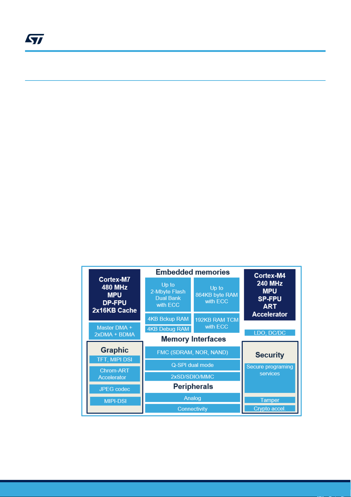
The figure below shows the main components of the STM32H7 dual‑core MCUs.
AN5557
System overview
®
Figure 1. STM32H7 dual‑core block diagram
AN5557 - Rev 1
page 3/36

2.1 Dual-core system
The STM32H7 dual‑core devices embed two Arm® cores, a Cortex®‑M7 and a Cortex®‑M4. The Cortex®‑M4
offers optimal performance for real‑time applications while the Cortex®‑M7 core can execute high‑performance
tasks in parallel.
The two cores belong to separate power domains; the Cortex®‑M7 core belongs to D1 domain and the
Cortex®‑M4 core belongs to D2 domain. Thanks to this independency, when an application does not require
for example the Cortex®‑M4, developers can turn its power domain off without any impact on the Cortex®‑M7
core and optimize energy consumption significantly. This dual‑core architecture is highly flexible and designed to
deliver a very high level of performance in combination with the low‑power modes already available on all STM32
microcontrollers.
The STM32H7 dual-core devices are among STM32 microcontrollers that embed more than one bus matrix.
Giving the best compromise between performance and power consumption. It also allows efficient simultaneous
operation of high‑speed peripherals and removes bus congestion when several masters are simultaneously
active (different masters located in separated bus matrices). The STM32H7 dual‑core feature three separate bus
matrices. Each bus matrix is associated to a domain:
1. The 64‑bit AXI bus matrix (in the D1 domain): It has a high‑performance capability and is dedicated to
operations requiring high transfer speed. The high bandwidth peripherals are connected to the AXI bus
matrix.
2. The 32‑bit AHB bus matrix (in the D2 domain): communication peripherals and timers are connected to this
bus matrix.
3. The 32‑bit AHB bus matrix (in the D3 domain): reset, clock control, power management and GPIOs are in
this domain.
The Cortex®‑M4 and all bus matrices can run up to 240 MHz. Only the Cortex®‑M7, the ITCM‑RAM and the
DTCM‑RAM can run up to 480 MHz. All bus matrices are connected together by means of inter‑domain buses to
allow a master located in a given domain to have access to a slave located in another domain, except for BDMA
master which access is limited to resources located in the D3 domain. An AXI bus matrix, two AHB bus matrices
and bus bridges allow interconnecting bus masters with bus slaves, as illustrated in Table 1 and Figure 2.
Note: For more details about system and bus architecture refer to the RM0399 “STM32H745/755 and
STM32H747/757 advanced Arm
®
‑
based 32‑bit MCUs”, available from the ST website www.st.com.
AN5557
Dual-core system
AN5557 - Rev 1
page 4/36

Table 1. Bus-master-to-slave interconnection
Bus master / type
AN5557
Dual-core system
LTDC
DMA2D
DMA1 - MEM
DMA1 - PERIPH
Interconnect path and type
DMA2 - MEM
DMA2 - PERIPH
(2)
USBHS1 - AHB
SDMMC2 - AHB
Eth. MAC - AHB
USBHS2 - AHB
Cortex-M4 - S-bus
Cortex-M4 - D-bus
Cortex-M4 - I-bus
Bus slave /
(1)
type
Cortex-M7 - AXIM
Cortex-M7 - ITCM
Cortex-M7 - AHBP
MDMA
SDMMC1
Cortex-M7 - DTCM
MDMA - AHBS
ITCM - - X - - - X - - - - - - - - - - - - - -
DTCM - - - X - X - - - - - - - - - - - - - -
AHB3
periphs
APB3
periphs
Flash bank
1
Flash bank
2
X - - - - X - - - X X X X X X X X X X X -
X - - - - X - - - X X X X X X X X X X X -
X - - - X X - X X X X X X X X X X X X X -
X - - - X X - X X X X X X X X X X X X X -
AXI SRAM X - - - X X - X X X X X X X X X X X X X -
QUADSPI X - - - X X - X X X X X X X X X X X X X -
FMC X - - - X X - X X X X X X X X X X X X X -
SRAM 1 X - - - - X - X - X X X X X X X X X X X -
SRAM 2 X - - - - X - X - X X X X X X X X X X X -
SRAM 3 X - - - - X - X - X X X X X X X X X X X -
AHB1
periphs
APB1
periphs
AHB2
periphs
APB2
periphs
AHB4
periphs
APB4
periphs
- X - - - X - X - X X X X - - - - X - - -
- X - - - X - X - X X X X - - - - X - - -
- X - - - X - X - X X X X - - - - X - - -
- X - - - X - X - X X X X - - - - X - - -
X - - - - X - - - X X X X X X X X X - - X
X - - - - X - - - X X X X X X X X X - - X
SRAM4 X - - - - X - - - X X X X X X X X X - - X
Backup RAM X - - - - X - - - X X X X X X X X X - - X
BDMA - AHB
1. Bold font type denotes 64-bit bus, plain type denotes 32-bit bus.
2. “X” = access possible, “-” = access not possible.
AN5557 - Rev 1
page 5/36
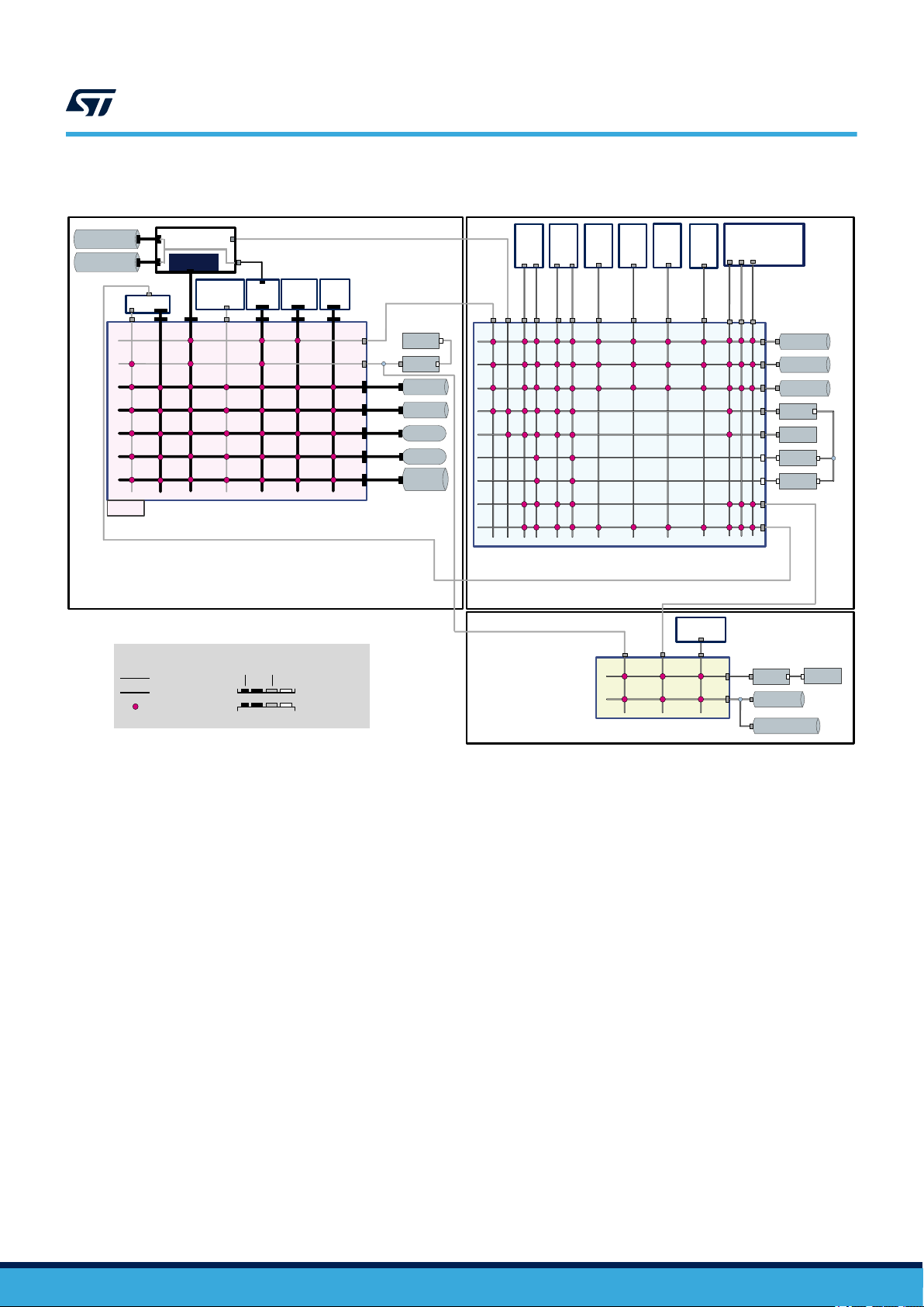
Figure 2. STM32H7 dual‑core system architecture
AN5557
Dual-core system
ITCM-RAM
DTCM-RAM
GPV
Legend
ITCM
L1-Cache
Cortex
(1)
L1-Cache
DTCM
AXIM
ART
D2-to-D1 AHB bus
32-bit bus
64-bit bus
Bus multiplexer
AHBP
®
-M7
AHBS
SDMMC1 MDMA
64-bit AXI bus matrix
D1 Domain
AHB
TCM
AXI
DMA2D
APB
Master interface
Slave interface
LTDC
D1-to-D2 AHB bus
AHB
APB3
AHB
AHB3
AXI
Flash A
AXI
Flash B
AXI
FMC
AXI
QSPI
AXI
AXI
SRAM
APB
D1-to-D3 AHB bus
DMA1
DMA2
DMA1_MEM
DMA2_MEM
DMA2_PERIPH
DMA1_PERIPH
32-bit AHB bus matrix
MAC
Ethernet
SDMMC2
D2 Domain
32-bit AHB bus matrix
D3 Domain
HS1
USB
HS2
USB
D2-to-D1 AHB bus
BDMA
®
Cortex
-M4
I-Bus
D-Bus
S-Bus
SRAM1
SRAM2
SRAM3
AHB1
AHB2
APB1
APB2
D2-to-D3 AHB bus
AHB4
SRAM4
Bckp SRAM
APB
APB4
As illustrated in the Figure 2, the STM32H7 dual‑core devices embed a reduced ART (adaptive real-time) memory
access Accelerator between the D2-to-D1 AHB and the AXI bus matrix. The ART Accelerator is mainly composed
of AHB switch, cache manager and 64 cache lines of 256 bits as shown in Figure 3.
AN5557 - Rev 1
page 6/36
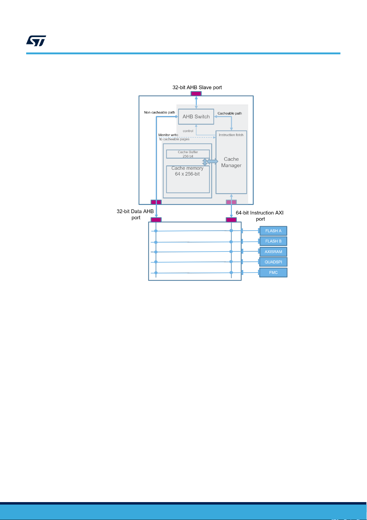
Figure 3. ART block diagram
AN5557
Memory resource assignment
It accelerates cacheable AHB instruction fetch accesses, using a dedicated 64-bit AXI bus matrix port to pre-fetch
code from the internal and external memories of the D1 domain into a built-in cache. It routes all the other AHB
accesses to a dedicated 32-bit AXI bus matrix port connecting the D2-to-D1 AHB with all the internal and external
memories and peripherals of the D1 domain excluding GPV, as well as with the D1-to-D3 AHB. As a consequence
the access of DMAs, Ethernet, except CM4, is always through data 32-bit AHB path.
Note: For more details about ART Accelerator refer to the reference manual RM0399 “STM32H745/755 and
STM32H747/757 advanced Arm®-based 32-bit MCUs”, available from the ST website www.st.com.
2.2
Memory resource assignment
2.2.1 Embedded SRAM
The STM32H7 dual‑core devices feature:
• Up to 864 Kbytes of System SRAM
• 128 Kbytes of data TCM RAM, DTCM RAM
• 64 Kbytes of instruction TCM RAM, ITCM RAM
• 4 Kbytes of backup SRAM
The embedded system SRAM is split into five blocks over the three power domains: AXI SRAM, AHB SRAM1,
AHB SRAM2, AHB SRAM3 and AHB SRAM4.
• D1 domain, AXI SRAM:
– AXI SRAM is accessible through D1 domain AXI bus matrix. It is mapped at address 0x2400 0000 and
accessible by all system masters except BDMA. AXI SRAM can be used for application data which are
not allocated in DTCM RAM or reserved for graphic objects (such as frame buffers)
AN5557 - Rev 1
page 7/36

AN5557
Memory resource assignment
• D2 domain, AHB SRAM:
– AHB SRAM1 is accessible through D2 domain AHB matrix. It is mapped at address 0x3000 0000 and
accessible by all system masters except BDMA. The AHB SRAMs of the D2 domain are also aliased
to an address range below 0x2000 0000 to maintain the Cortex®‑M4 Harvard architecture. The AHB
SRAM1 also mapped at address 0x1000 0000. The AHB SRAM2 also mapped at address 0x1002
0000. The AHB SRAM3 also mapped at address 0x1004 0000. All those AHB SRAMs are accessible
by all system masters through D2 domain AHB matrix. All those AHB SRAMs are accessible by all
system masters through D2 domain AHB matrix.
AHB SRAM1 can be used as DMA buffers to store peripheral input/output data in D2 domain, or as
code location for Cortex®‑M4 CPU (application code available when D1 is powered off). AHB SRAM1
can be used as DMA buffers to store peripheral input/output data in D2 domain, or as code location for
Cortex®‑M4 CPU (application code available when D1 is powered off).
– AHB SRAM2 is accessible through D2 domain AHB matrix. It is mapped at address 0x3002 0000
and accessible by all system masters except BDMA. AHB SRAM2 can be used as DMA buffers to
store peripheral input/output data in D2 domain, or as readwrite segment for application running on
Cortex®‑M4 CPU.
– AHB SRAM3 is accessible through D2 domain AHB matrix is mapped at address 0x3004 0000
and accessible by all system masters except BDMA. AHB SRAM3 can be used as buffers to store
peripheral input/output data for Ethernet and USB, or as shared memory between the two cores.
• D3 domain, AHB SRAM:
– AHB SRAM4 is mapped at address 0x3800 0000 and accessible by most of system masters through
D3 domain AHB matrix. AHB SRAM4 can be used as BDMA buffers to store peripheral input/output
data in D3 domain. It can also be used to retain some application code/data when D1 and D2 domain
in DStandby mode, or as shared memory between the two cores.
The system AHB SRAM can be accessed as bytes, half‑words (16‑bit units) or words (32‑bit units), while the
system AXI SRAM can be accessed as bytes, half‑words, words or doublewords (64‑bit units). These memories
can be addressed at maximum system clock frequency without wait state.
2.2.2 Flash memory
The embedded Flash memory is a central resource for the whole microcontroller. The embedded Flash memory
also proposes a set of security features to protect the assets stored in the non-volatile memory at boot time, at
run-time and during firmware and configuration upgrades.
The embedded Flash memory offers two 64-bit AXI slave ports for code and data accesses, plus a 32-bit AHB
configuration slave port used for register bank accesses. The STM32H7 dual‑core devices embed 2 Mbytes of
Flash memory that can be used for storing programs and data. The Flash memory is organized as 266-bit Flash
words memory that can be used for storing both code and data constants. Each word consists of:
• One Flash word (8 words, 32 bytes or 256 bits)
• 10 ECC bits.
The Flash memory is divided into two independent banks. Each bank is organized as follows:
• 1 Mbyte of user Flash memory block containing eight user sectors of 128 Kbytes (4 K Flash memory words)
• 128 Kbytes of System Flash memory from which the device can boot 2 Kbytes (64 Flash words) of user
option bytes for user configuration
Note: For more details about memory mapping refer to the reference manual RM0399 “STM32H745/755 and
STM32H747/757 advanced Arm
®
‑
based 32‑bit MCUs”, available from the ST website www.st.com.
AN5557 - Rev 1
page 8/36
2.3 Peripherals allocation
The peripheral allocation is used by the reset and clock controller (RCC), to automatically control the clock gating
according to the CPUs and domain modes, and by the power controller (PWR) to control the supply voltages
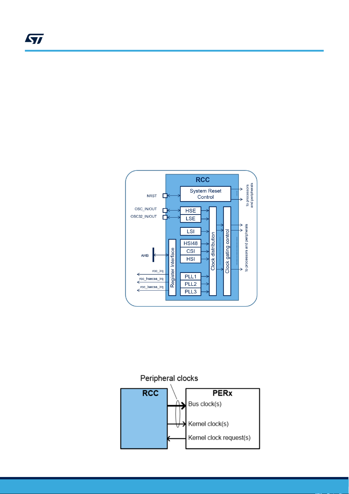
of D1, D2 and D3 domains. As presented in Figure 4. RCC block diagram, the RCC is mainly composed by
the system reset control, the clock distribution, the clock gating control, the register interface, and different clock
sources. The clock gating control is responsible for the peripheral allocation. The RCC manages the reset, the
system and peripheral clocks generation. It uses four internal oscillators, two oscillators for an external crystal or
resonator, and three phase-locked loops (PLL). Therefore, many peripherals have their own clock, independent
of the system clock. The RCC provides high flexibility in the choice of clock sources, which allows the system
designers to meet both power consumption and accuracy requirements. The numerous independent peripheral
clocks allow a designer to adjust the system power consumption without impacting the communication baud rates,
and to keep some peripherals active in low-power mode.
AN5557
Peripherals allocation
Figure 4. RCC block diagram
AN5557 - Rev 1
Many peripheral in STM32H7 dual
bus interface, and the clock for the peripheral specific interface. Generally, the clocks for the data and control
streams via the processor bus interface are named ‘Bus clock’, and the clock for the peripheral specific interface
are named ‘kernel clocks’.
As shown in Figure 5, the peripheral clocks represent the clocks received by the peripheral: ‘bus clock’ and
‘kernel clock’.
‑core, have different clocks for the data and control streams via the processor
Figure 5. Peripheral clock exchange
page 9/36
AN5557
Peripherals allocation
Having a separate bus clock and kernel clock allows the application to change the interconnect and processor
working frequency without affecting the peripheral. For some peripheral it is also possible to disable the bus
clock as long as the peripheral does not need to transfer data to the system. So, it gives a good flexibility on
the frequency selection for the bus processor and memories, and the real need of the peripheral interface. For
example, the UARTs have a kernel clock which is used, among other things, by the baud rate generator for
the serial interface communication, and an APB clock for the register interface. Thus if the system clock has
changed the baud rate is not affected. In addition, some peripherals are able to request the kernel clock when
they detected specific events.
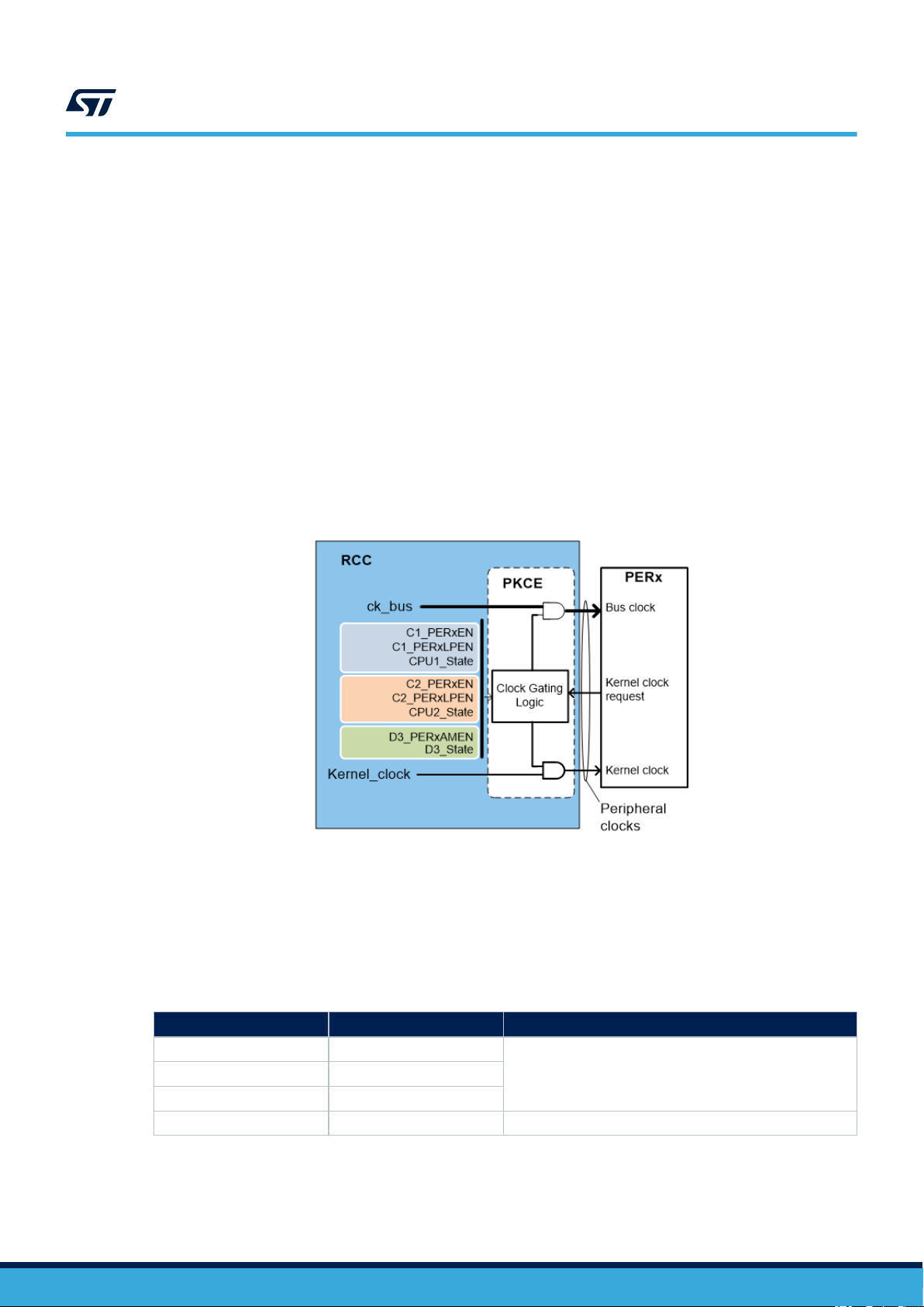
As mentioned before, the peripherals generally receive two types of clocks: bus clock and kernel clock. Those
clocks can be one or several for each peripheral. Each processor can control the clock gating of the peripheral
clocks via dedicated registers located into the RCC.
As illustrated in Figure 6, the gating of the peripheral clocks depends on several parameters:
• The clock enables bits, each processor has a dedicated control bit for that, named C1_PERxEN and
C2_PERxEN
• The low-power clock enables bits : C1_PERxLPEN and C2_PERxLPEN
• The processors states: CRUN, CSLEEP or CSTOP
• The autonomous bits for peripherals located in D3 domain: D3_PERxAMEN
Figure 6. Peripheral clock gating
AN5557 - Rev 1
In Table 2, the operation of peripheral allocation is describing as below:
• When setting the bit C1_PERxEN to ‘1’ indicates that the peripheral PERx is enabled for the CPU1
• When setting the bit C2_PERxEN to ‘1’ indicates that the peripheral PERx is enabled for the CPU2
• When both C1_PERxEN/C2_PERxEN are set, the peripheral clock follows the two CPU states. For
example, if CPU1 is in stop, and CPU2 is in run the clock to the peripheral remains enabled
Table 2. Peripheral clock allocation
CPU1
CRUN CSTOP
CSTOP CRUN
CSTOP CSTOP Disabled
CPU2 Peripheral clock
EnabledCRUN CRUN
page 10/36
It is important to notice that the RCC offers two register sets, allowing each processor to enable or allocate
peripherals. The peripheral allocation informs the RCC that the CPU1 or CPU2 enabled a peripheral. This
information is used by the RCC for the clock control in low-power modes. So before using a peripheral the CPUs
must allocate it. The same peripheral can be allocated by both processors, it is up to the application to avoid
resources conflicts.
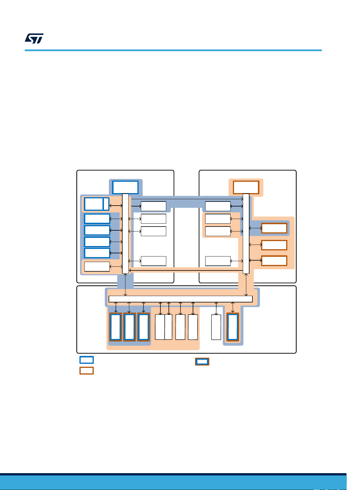
As introduced in the figure below, some peripherals are implicitly allocated to a processor:
• The FLASH, D1SRAM1, ITCM, DTCM1 and DTCM2 are implicitly allocated to CPU1, the CPU2 can allocate
any of them, but by default they are not allocated to CPU2.
• The D2SRAM1, D2SRAM2 and D2SRAM3 are implicitly allocated to CPU2, the CPU1 can allocate any of
them, but by default they are not allocated to CPU1.
Note: Implicitly means architecturally tied to a processor.
Figure 7. Peripheral allocation
AN5557
Peripherals allocation
FLASH
AXISRAM
ITCM
DTCM1
DTCM2
ART
D3
FLITF
D1
CPU1
IWDG1
SDMMC1
PER...
PER...
Bus Matrix 1
PER...
IWDG2
RCC
...
DMA1
CPU1_SS
CPU2_SS
Bus Matrix 3
DMAMUX
I2C4
SAI4
SPI5
SAI1
I2C2
PER...
PER...
...
D2
CPU2
Bus Matrix 2
SRAM1
...
SRAM4
SRAM2
SRAM3
Peripherals implicitly allocated to CPU1
Peripherals implicitly allocated to CPU2
Peripherals implicitly allocated to both
CPUs
Some other peripherals are implicitly allocated to both processors, this is the case for the IWDG1, IWDG2, RCC,
PWR, AIEC and D3SRAM1. When a CPU allocates a peripheral, this peripheral is linked to the processor state
for the low-power modes. The CPU, plus the peripherals allocated by this CPU, and the associated interconnect
is considered by the RCC as a CPU sub-system. The D1 and D2 domain core voltage can be switched-off. To
give a simple example of the use of the peripheral allocation by the RCC, the RCC doesn't allow a domain to
be switched-off, if one of the peripheral of this domain is used by the processor of the other domain which is not
switched-off.
Note: For more details about peripherals allocation, refer to the application note AN5215 “STM32H747/757 advanced
power management”, available from the ST website www.st.com.
AN5557 - Rev 1
page 11/36
 Loading...