

Datasheet STM32H747AI, STM32H747BI, STM32H747II, STM32H747XI, STM32H747ZI Datasheet (STMicroelectronics)
...Page 1
STM32H747xI/G
UFBGA169
(7 × 7 mm)
TFBGA240+25
(14x14 mm)
LQFP176
(24x24 mm)
LQFP208
(28x28 mm)
WLCSP156
(4.96x4.64 mm)
Dual 32-bit Arm® Cortex®-M7 up to 480MHz and -M4 MCUs, up to
2MB Flash, 1MB RAM, 46 com. and analog interfaces, SMPS, DSI
Datasheet - production data
Features
Dual core
• 32-bit Arm® Cortex®-M7 core with double-
precision FPU and L1 cache: 16 Kbytes of data
and 16 Kbytes of instruction cache; frequency
up to 480 MHz, MPU, 1027 DMIPS/
2.14 DMIPS/MHz (Dhrystone 2.1), and DSP
instructions
• 32-bit Arm
Adaptive real-time accelerator (ART
Accelerator™) for internal Flash memory and
external memories, frequency up to 240 MHz,
MPU, 300 DMIPS/1.25 DMIPS /MHz
(Dhrystone 2.1), and DSP instructions
Memories
• Up to 2 Mbytes of Flash memory with readwhile-write support
• 1 Mbyte of RAM: 192 Kbytes of TCM RAM (inc.
64 Kbytes of ITCM RAM + 128 Kbytes of
DTCM RAM for time critical routines),
864 Kbytes of user SRAM, and 4 Kbytes of
SRAM in Backup domain
• Dual mode Quad-SPI memory interface
running up to 133 MHz
• Flexible external memory controller with up to
32-bit data bus: SRAM, PSRAM,
SDRAM/LPSDR SDRAM, NOR/NAND Flash
memory clocked up to 125 MHz in
Synchronous mode
• CRC calculation unit
®
32-bit Cortex®-M4 core with FPU,
FBGA
Reset and power management
• 3 separate power domains which can be
independently clock-gated or switched off:
– D1: high-performance capabilities
– D2: communication peripherals and timers
– D3: reset/clock control/power management
• 1.62 to 3.6 V application supply and I/Os
• POR, PDR, PVD and BOR
• Dedicated USB power embedding a 3.3 V
internal regulator to supply the internal PHYs
• Embedded regulator (LDO) to supply the digital
circuitry
• High power-efficiency SMPS step-down
converter regulator to directly supply V
and/or external circuitry
• Voltage scaling in Run and Stop mode (6
configurable ranges)
• Backup regulator (~0.9 V)
• Voltage reference for analog peripheral/V
• 1.2 to 3.6 V V
BAT
supply
• Low-power modes: Sleep, Stop, Standby and
V
supporting battery charging
BAT
CORE
REF+
Security
• ROP, PC-ROP, active tamper
Low-power consumption
• V
battery operating mode with charging
BAT
capability
General-purpose input/outputs
• Up to 168 I/O ports with interrupt capability
• CPU and domain power state monitoring pins
• 2.95 µA in Standby mode (Backup SRAM OFF,
RTC/LSE ON)
May 2019 DS12930 Rev 1 1/242
This is information on a product in full production.
www.st.com
Page 2

STM32H747xI/G
Clock management
• Internal oscillators: 64 MHz HSI, 48 MHz
HSI48, 4 MHz CSI, 32 kHz LSI
• External oscillators: 4-48 MHz HSE,
32.768 kHz LSE
• 3× PLLs (1 for the system clock, 2 for kernel
clocks) with Fractional mode
Interconnect matrix
• 3 bus matrices (1 AXI and 2 AHB)
• Bridges (5× AHB2-APB, 2× AXI2-AHB)
4 DMA controllers to unload the CPU
• 1× high-speed master direct memory access
controller (MDMA) with linked list support
• 2× dual-port DMAs with FIFO
• 1× basic DMA with request router capabilities
Up to 35 communication peripherals
• 4× I2Cs FM+ interfaces (SMBus/PMBus)
• 4× USARTs/4x UARTs (ISO7816 interface,
LIN, IrDA, up to 12.5 Mbit/s) and 1x LPUART
• 6× SPIs, 3 with muxed duplex I2S audio class
accuracy via internal audio PLL or external
clock, 1x I2S in LP domain (up to 150 MHz)
• 4x SAIs (serial audio interface)
• SPDIFRX interface
• SWPMI single-wire protocol master I/F
• MDIO Slave interface
• 2× SD/SDIO/MMC interfaces (up to 125 MHz)
• 2× CAN controllers: 2 with CAN FD, 1 with
time-triggered CAN (TT-CAN)
• 2× USB OTG interfaces (1FS, 1HS/FS) crystalless solution with LPM and BCD
• Ethernet MAC interface with DMA controller
• HDMI-CEC
• 8- to 14-bit camera interface (up to 80 MHz)
11 analog peripherals
• 2× operational amplifiers (7.3 MHz bandwidth)
• 1× digital filters for sigma delta modulator
(DFSDM) with 8 channels/4 filters
Graphics
• LCD-TFT controller up to XGA resolution
• MIPI DSI host including an MIPI D-PHY to
interface with low-pin count large displays
• Chrom-ART graphical hardware Accelerator™
(DMA2D) to reduce CPU load
• Hardware JPEG Codec
Up to 22 timers and watchdogs
• 1× high-resolution timer (2.1 ns max
resolution)
• 2× 32-bit timers with up to 4 IC/OC/PWM or
pulse counter and quadrature (incremental)
encoder input (up to 240 MHz)
• 2× 16-bit advanced motor control timers (up to
240 MHz)
• 10× 16-bit general-purpose timers (up to
240 MHz)
• 5× 16-bit low-power timers (up to 240 MHz)
• 4× watchdogs (independent and window)
• 2× SysTick timers
• RTC with sub-second accuracy and hardware
calendar
Debug mode
• SWD & JTAG interfaces
• 4-Kbyte Embedded Trace Buffer
True random number generators (3
oscillators each)
96-bit unique ID
All packages are ECOPACK
Table 1. Device summary
Reference Part number
®
2 compliant
• 3× ADCs with 16-bit max. resolution (up to 36
channels, up to 3.6 MSPS)
• 1× temperature sensor
• 2× 12-bit D/A converters (1 MHz)
• 2× ultra-low-power comparators
2/242 DS12930 Rev 1
STM32H747xISTM32H747AI, STM32H747BI,
STM32H747xGSTM32H747AG, STM32H747BG,
STM32H747II, STM32H747XI, STM32H747ZI
STM32H747IG, STM32H747XG
Page 3

STM32H747xI/G Contents
Contents
1 Introduction . . . . . . . . . . . . . . . . . . . . . . . . . . . . . . . . . . . . . . . . . . . . . . . . 3
2 Description . . . . . . . . . . . . . . . . . . . . . . . . . . . . . . . . . . . . . . . . . . . . . . . . . 4
3 Functional overview . . . . . . . . . . . . . . . . . . . . . . . . . . . . . . . . . . . . . . . . 11
3.1 Dual Arm® Cortex® cores . . . . . . . . . . . . . . . . . . . . . . . . . . . . . . . . . . . . . .11
3.1.1 Arm® Cortex®-M7 with FPU . . . . . . . . . . . . . . . . . . . . . . . . . . . . . . . . . . 11
3.1.2 Arm
3.2 Memory protection unit (MPU) . . . . . . . . . . . . . . . . . . . . . . . . . . . . . . . . . 12
3.3 Memories . . . . . . . . . . . . . . . . . . . . . . . . . . . . . . . . . . . . . . . . . . . . . . . . . 13
3.3.1 Embedded Flash memory . . . . . . . . . . . . . . . . . . . . . . . . . . . . . . . . . . . 13
3.3.2 Embedded SRAM . . . . . . . . . . . . . . . . . . . . . . . . . . . . . . . . . . . . . . . . . 13
3.3.3 ART™ accelerator . . . . . . . . . . . . . . . . . . . . . . . . . . . . . . . . . . . . . . . . . 14
®
Cortex®-M4 with FPU . . . . . . . . . . . . . . . . . . . . . . . . . . . . . . . . . . 12
3.4 Boot modes . . . . . . . . . . . . . . . . . . . . . . . . . . . . . . . . . . . . . . . . . . . . . . . 15
3.5 Power supply management . . . . . . . . . . . . . . . . . . . . . . . . . . . . . . . . . . . 16
3.5.1 Power supply scheme . . . . . . . . . . . . . . . . . . . . . . . . . . . . . . . . . . . . . . 16
3.5.2 Power supply supervisor . . . . . . . . . . . . . . . . . . . . . . . . . . . . . . . . . . . . 17
3.5.3 Voltage regulator (SMPS step-down converter and LDO) . . . . . . . . . . . 18
3.5.4 SMPS step-down converter . . . . . . . . . . . . . . . . . . . . . . . . . . . . . . . . . . 18
3.6 Low-power strategy . . . . . . . . . . . . . . . . . . . . . . . . . . . . . . . . . . . . . . . . . 19
3.7 Reset and clock controller (RCC) . . . . . . . . . . . . . . . . . . . . . . . . . . . . . . . 20
3.7.1 Clock management . . . . . . . . . . . . . . . . . . . . . . . . . . . . . . . . . . . . . . . . 20
3.7.2 System reset sources . . . . . . . . . . . . . . . . . . . . . . . . . . . . . . . . . . . . . . 21
3.8 General-purpose input/outputs (GPIOs) . . . . . . . . . . . . . . . . . . . . . . . . . . 21
3.9 Bus-interconnect matrix . . . . . . . . . . . . . . . . . . . . . . . . . . . . . . . . . . . . . . 21
3.10 DMA controllers . . . . . . . . . . . . . . . . . . . . . . . . . . . . . . . . . . . . . . . . . . . . 23
3.11 Chrom-ART Accelerator™ (DMA2D) . . . . . . . . . . . . . . . . . . . . . . . . . . . . 23
3.12 Nested vectored interrupt controller (NVIC) . . . . . . . . . . . . . . . . . . . . . . . 24
3.13 Extended interrupt and event controller (EXTI) . . . . . . . . . . . . . . . . . . . . 24
3.14 Cyclic redundancy check calculation unit (CRC) . . . . . . . . . . . . . . . . . . . 24
3.15 Flexible memory controller (FMC) . . . . . . . . . . . . . . . . . . . . . . . . . . . . . . 25
3.16 Quad-SPI memory interface (QUADSPI) . . . . . . . . . . . . . . . . . . . . . . . . . 25
DS12930 Rev 1 1/242
4
Page 4

Contents STM32H747xI/G
3.17 Analog-to-digital converters (ADCs) . . . . . . . . . . . . . . . . . . . . . . . . . . . . . 25
3.18 Temperature sensor . . . . . . . . . . . . . . . . . . . . . . . . . . . . . . . . . . . . . . . . . 26
3.19 V
operation . . . . . . . . . . . . . . . . . . . . . . . . . . . . . . . . . . . . . . . . . . . . . 26
BAT
3.20 Digital-to-analog converters (DAC) . . . . . . . . . . . . . . . . . . . . . . . . . . . . . 27
3.21 Ultra-low-power comparators (COMP) . . . . . . . . . . . . . . . . . . . . . . . . . . . 27
3.22 Operational amplifiers (OPAMP) . . . . . . . . . . . . . . . . . . . . . . . . . . . . . . . 27
3.23 Digital filter for sigma-delta modulators (DFSDM) . . . . . . . . . . . . . . . . . . 28
3.24 Digital camera interface (DCMI) . . . . . . . . . . . . . . . . . . . . . . . . . . . . . . . . 29
3.25 LCD-TFT controller . . . . . . . . . . . . . . . . . . . . . . . . . . . . . . . . . . . . . . . . . . 30
3.26 DSI Host (DSI) . . . . . . . . . . . . . . . . . . . . . . . . . . . . . . . . . . . . . . . . . . . . . 30
3.27 JPEG Codec (JPEG) . . . . . . . . . . . . . . . . . . . . . . . . . . . . . . . . . . . . . . . . 31
3.28 Random number generator (RNG) . . . . . . . . . . . . . . . . . . . . . . . . . . . . . . 32
3.29 Timers and watchdogs . . . . . . . . . . . . . . . . . . . . . . . . . . . . . . . . . . . . . . . 32
3.29.1 High-resolution timer (HRTIM1) . . . . . . . . . . . . . . . . . . . . . . . . . . . . . . . 34
3.29.2 Advanced-control timers (TIM1, TIM8) . . . . . . . . . . . . . . . . . . . . . . . . . 35
3.29.3 General-purpose timers (TIMx) . . . . . . . . . . . . . . . . . . . . . . . . . . . . . . . 35
3.29.4 Basic timers TIM6 and TIM7 . . . . . . . . . . . . . . . . . . . . . . . . . . . . . . . . . 36
3.29.5 Low-power timers (LPTIM1, LPTIM2, LPTIM3, LPTIM4, LPTIM5) . . . . 36
3.29.6 Independent watchdogs . . . . . . . . . . . . . . . . . . . . . . . . . . . . . . . . . . . . . 36
3.29.7 Window watchdogs . . . . . . . . . . . . . . . . . . . . . . . . . . . . . . . . . . . . . . . . 36
3.29.8 SysTick timer . . . . . . . . . . . . . . . . . . . . . . . . . . . . . . . . . . . . . . . . . . . . . 36
3.30 Real-time clock (RTC), backup SRAM and backup registers . . . . . . . . . . 37
3.31 Inter-integrated circuit interface (I
2
C) . . . . . . . . . . . . . . . . . . . . . . . . . . . . 38
3.32 Universal synchronous/asynchronous receiver transmitter (USART) . . . 38
3.33 Low-power universal asynchronous receiver transmitter (LPUART) . . . . 39
3.34 Serial peripheral interface (SPI)/inter- integrated sound interfaces (I2S) . 40
3.35 Serial audio interfaces (SAI) . . . . . . . . . . . . . . . . . . . . . . . . . . . . . . . . . . . 40
3.36 SPDIFRX Receiver Interface (SPDIFRX) . . . . . . . . . . . . . . . . . . . . . . . . . 41
3.37 Single wire protocol master interface (SWPMI) . . . . . . . . . . . . . . . . . . . . 41
3.38 Management Data Input/Output (MDIO) slaves . . . . . . . . . . . . . . . . . . . . 42
3.39 SD/SDIO/MMC card host interfaces (SDMMC) . . . . . . . . . . . . . . . . . . . . 42
3.40 Controller area network (FDCAN1, FDCAN2) . . . . . . . . . . . . . . . . . . . . . 42
3.41 Universal serial bus on-the-go high-speed (OTG_HS) . . . . . . . . . . . . . . . 43
3.42 Ethernet MAC interface with dedicated DMA controller (ETH) . . . . . . . . . 43
2/242 DS12930 Rev 1
Page 5

STM32H747xI/G Contents
3.43 High-definition multimedia interface (HDMI)
- consumer electronics control (CEC) . . . . . . . . . . . . . . . . . . . . . . . . . . . 44
3.44 Debug infrastructure . . . . . . . . . . . . . . . . . . . . . . . . . . . . . . . . . . . . . . . . . 44
4 Memory mapping . . . . . . . . . . . . . . . . . . . . . . . . . . . . . . . . . . . . . . . . . . . 46
5 Pin descriptions . . . . . . . . . . . . . . . . . . . . . . . . . . . . . . . . . . . . . . . . . . . 47
6 Electrical characteristics . . . . . . . . . . . . . . . . . . . . . . . . . . . . . . . . . . . . 96
6.1 Parameter conditions . . . . . . . . . . . . . . . . . . . . . . . . . . . . . . . . . . . . . . . . 96
6.1.1 Minimum and maximum values . . . . . . . . . . . . . . . . . . . . . . . . . . . . . . . 96
6.1.2 Typical values . . . . . . . . . . . . . . . . . . . . . . . . . . . . . . . . . . . . . . . . . . . . 96
6.1.3 Typical curves . . . . . . . . . . . . . . . . . . . . . . . . . . . . . . . . . . . . . . . . . . . . 96
6.1.4 Loading capacitor . . . . . . . . . . . . . . . . . . . . . . . . . . . . . . . . . . . . . . . . . 96
6.1.5 Pin input voltage . . . . . . . . . . . . . . . . . . . . . . . . . . . . . . . . . . . . . . . . . . 96
6.1.6 Power supply scheme . . . . . . . . . . . . . . . . . . . . . . . . . . . . . . . . . . . . . . 97
6.1.7 Current consumption measurement . . . . . . . . . . . . . . . . . . . . . . . . . . . 98
6.2 Absolute maximum ratings . . . . . . . . . . . . . . . . . . . . . . . . . . . . . . . . . . . . 98
6.3 Operating conditions . . . . . . . . . . . . . . . . . . . . . . . . . . . . . . . . . . . . . . . 100
6.3.1 General operating conditions . . . . . . . . . . . . . . . . . . . . . . . . . . . . . . . . 100
6.3.2 VCAP external capacitor . . . . . . . . . . . . . . . . . . . . . . . . . . . . . . . . . . . 103
6.3.3 SMPS step-down converter . . . . . . . . . . . . . . . . . . . . . . . . . . . . . . . . . 104
6.3.4 Operating conditions at power-up / power-down . . . . . . . . . . . . . . . . . 105
6.3.5 Embedded reset and power control block characteristics . . . . . . . . . . 106
6.3.6 Embedded reference voltage . . . . . . . . . . . . . . . . . . . . . . . . . . . . . . . . 107
6.3.7 Supply current characteristics . . . . . . . . . . . . . . . . . . . . . . . . . . . . . . . 108
6.3.8 Wakeup time from low-power modes . . . . . . . . . . . . . . . . . . . . . . . . . . 128
6.3.9 External clock source characteristics . . . . . . . . . . . . . . . . . . . . . . . . . . 129
6.3.10 Internal clock source characteristics . . . . . . . . . . . . . . . . . . . . . . . . . . 133
6.3.11 PLL characteristics . . . . . . . . . . . . . . . . . . . . . . . . . . . . . . . . . . . . . . . . 136
6.3.12 MIPI D-PHY characteristics . . . . . . . . . . . . . . . . . . . . . . . . . . . . . . . . . 137
6.3.13 MIPI D-PHY regulator characteristics . . . . . . . . . . . . . . . . . . . . . . . . . 140
6.3.14 Memory characteristics . . . . . . . . . . . . . . . . . . . . . . . . . . . . . . . . . . . . 141
6.3.15 EMC characteristics . . . . . . . . . . . . . . . . . . . . . . . . . . . . . . . . . . . . . . . 142
6.3.16 Absolute maximum ratings (electrical sensitivity) . . . . . . . . . . . . . . . . 144
6.3.17 I/O current injection characteristics . . . . . . . . . . . . . . . . . . . . . . . . . . . 145
6.3.18 I/O port characteristics . . . . . . . . . . . . . . . . . . . . . . . . . . . . . . . . . . . . . 146
DS12930 Rev 1 3/242
4
Page 6

Contents STM32H747xI/G
6.3.19 NRST pin characteristics . . . . . . . . . . . . . . . . . . . . . . . . . . . . . . . . . . . 153
6.3.20 FMC characteristics . . . . . . . . . . . . . . . . . . . . . . . . . . . . . . . . . . . . . . . 153
6.3.21 Quad-SPI interface characteristics . . . . . . . . . . . . . . . . . . . . . . . . . . . 175
6.3.22 Delay block (DLYB) characteristics . . . . . . . . . . . . . . . . . . . . . . . . . . . 177
6.3.23 16-bit ADC characteristics . . . . . . . . . . . . . . . . . . . . . . . . . . . . . . . . . . 178
6.3.24 DAC characteristics . . . . . . . . . . . . . . . . . . . . . . . . . . . . . . . . . . . . . . . 186
6.3.25 Voltage reference buffer characteristics . . . . . . . . . . . . . . . . . . . . . . . 190
6.3.26 Temperature sensor characteristics . . . . . . . . . . . . . . . . . . . . . . . . . . . 191
6.3.27 Temperature and V
6.3.28 Voltage booster for analog switch . . . . . . . . . . . . . . . . . . . . . . . . . . . . 192
6.3.29 Comparator characteristics . . . . . . . . . . . . . . . . . . . . . . . . . . . . . . . . . 193
6.3.30 Operational amplifier characteristics . . . . . . . . . . . . . . . . . . . . . . . . . . 194
6.3.31 Digital filter for Sigma-Delta Modulators (DFSDM) characteristics . . . 196
6.3.32 Camera interface (DCMI) timing specifications . . . . . . . . . . . . . . . . . . 199
6.3.33 LCD-TFT controller (LTDC) characteristics . . . . . . . . . . . . . . . . . . . . . 200
6.3.34 Timer characteristics . . . . . . . . . . . . . . . . . . . . . . . . . . . . . . . . . . . . . . 202
6.3.35 Communication interfaces . . . . . . . . . . . . . . . . . . . . . . . . . . . . . . . . . . 202
monitoring . . . . . . . . . . . . . . . . . . . . . . . . . . . . 192
BAT
7 Package information . . . . . . . . . . . . . . . . . . . . . . . . . . . . . . . . . . . . . . . 222
7.1 WLCSP156 package information . . . . . . . . . . . . . . . . . . . . . . . . . . . . . . 222
7.2 UFBGA169 package information . . . . . . . . . . . . . . . . . . . . . . . . . . . . . . 225
7.3 LQFP176 package information . . . . . . . . . . . . . . . . . . . . . . . . . . . . . . . . 227
7.4 LQFP208 package information . . . . . . . . . . . . . . . . . . . . . . . . . . . . . . . . 231
7.5 TFBGA240+25 package information . . . . . . . . . . . . . . . . . . . . . . . . . . . 235
7.6 Thermal characteristics . . . . . . . . . . . . . . . . . . . . . . . . . . . . . . . . . . . . . 238
7.6.1 Reference document . . . . . . . . . . . . . . . . . . . . . . . . . . . . . . . . . . . . . . 239
8 Ordering information . . . . . . . . . . . . . . . . . . . . . . . . . . . . . . . . . . . . . . 240
9 Revision history . . . . . . . . . . . . . . . . . . . . . . . . . . . . . . . . . . . . . . . . . . 241
4/242 DS12930 Rev 1
Page 7

STM32H747xI/G List of tables
List of tables
Table 1. Device summary . . . . . . . . . . . . . . . . . . . . . . . . . . . . . . . . . . . . . . . . . . . . . . . . . . . . . . . . . . 2
Table 1. STM32H747xI/G features and peripheral counts . . . . . . . . . . . . . . . . . . . . . . . . . . . . . . . . . 6
Table 2. System vs domain low-power mode . . . . . . . . . . . . . . . . . . . . . . . . . . . . . . . . . . . . . . . . . . 20
Table 3. DFSDM implementation . . . . . . . . . . . . . . . . . . . . . . . . . . . . . . . . . . . . . . . . . . . . . . . . . . . 29
Table 4. Timer feature comparison . . . . . . . . . . . . . . . . . . . . . . . . . . . . . . . . . . . . . . . . . . . . . . . . . . 32
Table 5. USART features . . . . . . . . . . . . . . . . . . . . . . . . . . . . . . . . . . . . . . . . . . . . . . . . . . . . . . . . . 39
Table 6. Legend/abbreviations used in the pinout table . . . . . . . . . . . . . . . . . . . . . . . . . . . . . . . . . . 52
Table 7. STM32H747xI/G pin/ball definition . . . . . . . . . . . . . . . . . . . . . . . . . . . . . . . . . . . . . . . . . . . 53
Table 8. Port A alternate functions . . . . . . . . . . . . . . . . . . . . . . . . . . . . . . . . . . . . . . . . . . . . . . . . . . 81
Table 9. Port B alternate functions . . . . . . . . . . . . . . . . . . . . . . . . . . . . . . . . . . . . . . . . . . . . . . . . . . 83
Table 10. Port C alternate functions . . . . . . . . . . . . . . . . . . . . . . . . . . . . . . . . . . . . . . . . . . . . . . . . . . 85
Table 11. Port D alternate functions . . . . . . . . . . . . . . . . . . . . . . . . . . . . . . . . . . . . . . . . . . . . . . . . . . 86
Table 12. Port E alternate functions . . . . . . . . . . . . . . . . . . . . . . . . . . . . . . . . . . . . . . . . . . . . . . . . . . 88
Table 13. Port F alternate functions . . . . . . . . . . . . . . . . . . . . . . . . . . . . . . . . . . . . . . . . . . . . . . . . . . 89
Table 14. Port G alternate functions . . . . . . . . . . . . . . . . . . . . . . . . . . . . . . . . . . . . . . . . . . . . . . . . . . 90
Table 15. Port H alternate functions . . . . . . . . . . . . . . . . . . . . . . . . . . . . . . . . . . . . . . . . . . . . . . . . . . 92
Table 16. Port I alternate functions. . . . . . . . . . . . . . . . . . . . . . . . . . . . . . . . . . . . . . . . . . . . . . . . . . . 93
Table 17. Port J alternate functions . . . . . . . . . . . . . . . . . . . . . . . . . . . . . . . . . . . . . . . . . . . . . . . . . . 94
Table 18. Port K alternate functions . . . . . . . . . . . . . . . . . . . . . . . . . . . . . . . . . . . . . . . . . . . . . . . . . . 95
Table 19. Voltage characteristics . . . . . . . . . . . . . . . . . . . . . . . . . . . . . . . . . . . . . . . . . . . . . . . . . . . . 98
Table 20. Current characteristics . . . . . . . . . . . . . . . . . . . . . . . . . . . . . . . . . . . . . . . . . . . . . . . . . . . . 99
Table 21. Thermal characteristics. . . . . . . . . . . . . . . . . . . . . . . . . . . . . . . . . . . . . . . . . . . . . . . . . . . . 99
Table 22. General operating conditions . . . . . . . . . . . . . . . . . . . . . . . . . . . . . . . . . . . . . . . . . . . . . . 100
Table 23. Supply voltage and maximum frequency configuration . . . . . . . . . . . . . . . . . . . . . . . . . . 103
Table 24. VCAP operating conditions . . . . . . . . . . . . . . . . . . . . . . . . . . . . . . . . . . . . . . . . . . . . . . . . 104
Table 25. Characteristics of SMPS step-down converter external components . . . . . . . . . . . . . . . . 104
Table 26. SMPS step-down converter characteristics for external usage . . . . . . . . . . . . . . . . . . . . 105
Table 27. Operating conditions at power-up / power-down (regulator ON) . . . . . . . . . . . . . . . . . . . 105
Table 28. Reset and power control block characteristics . . . . . . . . . . . . . . . . . . . . . . . . . . . . . . . . . 106
Table 29. Embedded reference voltage . . . . . . . . . . . . . . . . . . . . . . . . . . . . . . . . . . . . . . . . . . . . . . 107
Table 30. Internal reference voltage calibration values . . . . . . . . . . . . . . . . . . . . . . . . . . . . . . . . . . 108
Table 31. Typical and maximum current consumption in Run mode, code with data processing
running from ITCM for Cortex-M7 core, and Flash memory for Cortex-M4
(ART accelerator ON), LDO regulator ON . . . . . . . . . . . . . . . . . . . . . . . . . . . . . . . . . . . . 109
Table 32. Typical and maximum current consumption in Run mode, code with data processing
running from ITCM for Arm Cortex-M7 and Flash memory for Arm Cortex-M4,
ART accelerator ON, SMPS regulator . . . . . . . . . . . . . . . . . . . . . . . . . . . . . . . . . . . . . . . 109
Table 33. Typical and maximum current consumption in Run mode, code with data processing
running from Flash memory, both cores running, cache ON,
ART accelerator ON, LDO regulator ON . . . . . . . . . . . . . . . . . . . . . . . . . . . . . . . . . . . . . 110
Table 34. Typical and maximum current consumption in Run mode, code with data processing
running from Flash memory, both cores running, cache OFF,
ART accelerator OFF, LDO regulator ON. . . . . . . . . . . . . . . . . . . . . . . . . . . . . . . . . . . . . 110
Table 35. Typical and maximum current consumption in Run mode, code with data processing
running from ITCM, only Arm Cortex-M7 running, LDO regulator ON . . . . . . . . . . . . . . . 111
Table 36. Typical and maximum current consumption in Run mode, code with data processing
running from ITCM, only Arm Cortex-M7 running, SMPS regulator. . . . . . . . . . . . . . . . . 112
Table 37. Typical and maximum current consumption in Run mode, code with data processing
DS12930 Rev 1 1/242
4
Page 8

List of tables STM32H747xI/G
running from Flash memory, only Arm Cortex-M7 running, cache ON,
LDO regulator ON . . . . . . . . . . . . . . . . . . . . . . . . . . . . . . . . . . . . . . . . . . . . . . . . . . . . . . . 112
Table 38. Typical and maximum current consumption in Run mode, code with data processing
running from Flash memory, only Arm Cortex-M7 running, cache OFF,
LDO regulator ON . . . . . . . . . . . . . . . . . . . . . . . . . . . . . . . . . . . . . . . . . . . . . . . . . . . . . . . 113
Table 39. Typical and maximum current consumption batch acquisition mode,
LDO regulator ON . . . . . . . . . . . . . . . . . . . . . . . . . . . . . . . . . . . . . . . . . . . . . . . . . . . . . . . 113
Table 40. Typical and maximum current consumption in Run mode, code with data processing
running from Flash memory, only Arm Cortex-M4 running, ART accelerator ON,
LDO regulator ON . . . . . . . . . . . . . . . . . . . . . . . . . . . . . . . . . . . . . . . . . . . . . . . . . . . . . . . 114
Table 41. Typical and maximum current consumption in Run mode, code with data processing
running from Flash bank 2, only Arm Cortex-M4 running, ART accelerator ON,
SMPS regulator . . . . . . . . . . . . . . . . . . . . . . . . . . . . . . . . . . . . . . . . . . . . . . . . . . . . . . . . 114
Table 42. Typical and maximum current consumption in Stop, LDO regulator ON . . . . . . . . . . . . . 115
Table 43. Typical and maximum current consumption in Stop, SMPS regulator . . . . . . . . . . . . . . . 116
Table 44. Typical and maximum current consumption in Sleep mode, LDO regulator . . . . . . . . . . 117
Table 45. Typical and maximum current consumption in Sleep mode, SMPS regulator . . . . . . . . . 117
Table 46. Typical and maximum current consumption in Standby . . . . . . . . . . . . . . . . . . . . . . . . . . 118
Table 47. Typical and maximum current consumption in VBAT mode . . . . . . . . . . . . . . . . . . . . . . . 118
Table 48. Peripheral current consumption in Run mode . . . . . . . . . . . . . . . . . . . . . . . . . . . . . . . . . 123
Table 49. Low-power mode wakeup timings . . . . . . . . . . . . . . . . . . . . . . . . . . . . . . . . . . . . . . . . . . 128
Table 50. High-speed external user clock characteristics. . . . . . . . . . . . . . . . . . . . . . . . . . . . . . . . . 129
Table 51. Low-speed external user clock characteristics . . . . . . . . . . . . . . . . . . . . . . . . . . . . . . . . . 130
Table 52. 4-48 MHz HSE oscillator characteristics . . . . . . . . . . . . . . . . . . . . . . . . . . . . . . . . . . . . . 131
Table 53. Low-speed external user clock characteristics . . . . . . . . . . . . . . . . . . . . . . . . . . . . . . . . . 132
Table 54. HSI48 oscillator characteristics. . . . . . . . . . . . . . . . . . . . . . . . . . . . . . . . . . . . . . . . . . . . . 133
Table 55. HSI oscillator characteristics. . . . . . . . . . . . . . . . . . . . . . . . . . . . . . . . . . . . . . . . . . . . . . . 134
Table 56. CSI oscillator characteristics. . . . . . . . . . . . . . . . . . . . . . . . . . . . . . . . . . . . . . . . . . . . . . . 134
Table 57. LSI oscillator characteristics . . . . . . . . . . . . . . . . . . . . . . . . . . . . . . . . . . . . . . . . . . . . . . . 135
Table 58. PLL characteristics (wide VCO frequency range). . . . . . . . . . . . . . . . . . . . . . . . . . . . . . . 136
Table 59. PLL characteristics (medium VCO frequency range) . . . . . . . . . . . . . . . . . . . . . . . . . . . . 137
Table 60. MIPI D-PHY characteristics . . . . . . . . . . . . . . . . . . . . . . . . . . . . . . . . . . . . . . . . . . . . . . . 137
Table 61. MIPI D-PHY AC characteristics LP mode and HS/LP
transitions . . . . . . . . . . . . . . . . . . . . . . . . . . . . . . . . . . . . . . . . . . . . . . . . . . . . . . . . . . . . . 139
Table 62. DSI regulator characteristics. . . . . . . . . . . . . . . . . . . . . . . . . . . . . . . . . . . . . . . . . . . . . . . 140
Table 63. Flash memory characteristics . . . . . . . . . . . . . . . . . . . . . . . . . . . . . . . . . . . . . . . . . . . . . . 141
Table 64. Flash memory programming (single bank configuration nDBANK=1) . . . . . . . . . . . . . . . 141
Table 65. Flash memory endurance and data retention . . . . . . . . . . . . . . . . . . . . . . . . . . . . . . . . . . 142
Table 66. EMS characteristics . . . . . . . . . . . . . . . . . . . . . . . . . . . . . . . . . . . . . . . . . . . . . . . . . . . . . 142
Table 67. EMI characteristics . . . . . . . . . . . . . . . . . . . . . . . . . . . . . . . . . . . . . . . . . . . . . . . . . . . . . . 143
Table 68. ESD absolute maximum ratings . . . . . . . . . . . . . . . . . . . . . . . . . . . . . . . . . . . . . . . . . . . . 144
Table 69. Electrical sensitivities . . . . . . . . . . . . . . . . . . . . . . . . . . . . . . . . . . . . . . . . . . . . . . . . . . . . 144
Table 70. I/O current injection susceptibility . . . . . . . . . . . . . . . . . . . . . . . . . . . . . . . . . . . . . . . . . . . 145
Table 71. I/O static characteristics . . . . . . . . . . . . . . . . . . . . . . . . . . . . . . . . . . . . . . . . . . . . . . . . . . 146
Table 72. Output voltage characteristics for all I/Os except PC13, PC14, PC15 and PI8 . . . . . . . . 148
Table 73. Output voltage characteristics for PC13, PC14, PC15 and PI8 . . . . . . . . . . . . . . . . . . . . 149
Table 74. Output timing characteristics (HSLV OFF) . . . . . . . . . . . . . . . . . . . . . . . . . . . . . . . . . . . . 150
Table 75. Output timing characteristics (HSLV ON) . . . . . . . . . . . . . . . . . . . . . . . . . . . . . . . . . . . . . 152
Table 76. NRST pin characteristics . . . . . . . . . . . . . . . . . . . . . . . . . . . . . . . . . . . . . . . . . . . . . . . . . 153
Table 77. Asynchronous non-multiplexed SRAM/PSRAM/NOR read timings . . . . . . . . . . . . . . . . . 155
Table 78. Asynchronous non-multiplexed SRAM/PSRAM/NOR read-NWAIT timings . . . . . . . . . . . 155
Table 79. Asynchronous non-multiplexed SRAM/PSRAM/NOR write timings . . . . . . . . . . . . . . . . . 157
2/242 DS12930 Rev 1
Page 9

STM32H747xI/G List of tables
Table 80. Asynchronous non-multiplexed SRAM/PSRAM/NOR write-NWAIT timings. . . . . . . . . . . 157
Table 81. Asynchronous multiplexed PSRAM/NOR read timings. . . . . . . . . . . . . . . . . . . . . . . . . . . 159
Table 82. Asynchronous multiplexed PSRAM/NOR read-NWAIT timings . . . . . . . . . . . . . . . . . . . . 159
Table 83. Asynchronous multiplexed PSRAM/NOR write timings . . . . . . . . . . . . . . . . . . . . . . . . . . 160
Table 84. Asynchronous multiplexed PSRAM/NOR write-NWAIT timings . . . . . . . . . . . . . . . . . . . . 160
Table 85. Synchronous multiplexed NOR/PSRAM read timings . . . . . . . . . . . . . . . . . . . . . . . . . . . 162
Table 86. Synchronous multiplexed PSRAM write timings . . . . . . . . . . . . . . . . . . . . . . . . . . . . . . . . 164
Table 87. Synchronous non-multiplexed NOR/PSRAM read timings . . . . . . . . . . . . . . . . . . . . . . . . 166
Table 88. Synchronous non-multiplexed PSRAM write timings . . . . . . . . . . . . . . . . . . . . . . . . . . . . 168
Table 89. Switching characteristics for NAND Flash read cycles . . . . . . . . . . . . . . . . . . . . . . . . . . . 171
Table 90. Switching characteristics for NAND Flash write cycles. . . . . . . . . . . . . . . . . . . . . . . . . . . 171
Table 91. SDRAM read timings . . . . . . . . . . . . . . . . . . . . . . . . . . . . . . . . . . . . . . . . . . . . . . . . . . . . 173
Table 92. LPSDR SDRAM read timings . . . . . . . . . . . . . . . . . . . . . . . . . . . . . . . . . . . . . . . . . . . . . . 173
Table 93. SDRAM Write timings . . . . . . . . . . . . . . . . . . . . . . . . . . . . . . . . . . . . . . . . . . . . . . . . . . . . 174
Table 94. LPSDR SDRAM Write timings . . . . . . . . . . . . . . . . . . . . . . . . . . . . . . . . . . . . . . . . . . . . . 175
Table 95. QUADSPI characteristics in SDR mode . . . . . . . . . . . . . . . . . . . . . . . . . . . . . . . . . . . . . . 175
Table 96. QUADSPI characteristics in DDR mode . . . . . . . . . . . . . . . . . . . . . . . . . . . . . . . . . . . . . . 176
Table 97. Delay Block characteristics . . . . . . . . . . . . . . . . . . . . . . . . . . . . . . . . . . . . . . . . . . . . . . . . 177
Table 98. ADC characteristics . . . . . . . . . . . . . . . . . . . . . . . . . . . . . . . . . . . . . . . . . . . . . . . . . . . . . 178
Table 99. Minimum sampling time vs RAIN . . . . . . . . . . . . . . . . . . . . . . . . . . . . . . . . . . . . . . . . . . . 181
Table 100. ADC accuracy. . . . . . . . . . . . . . . . . . . . . . . . . . . . . . . . . . . . . . . . . . . . . . . . . . . . . . . . . . 183
Table 101. DAC characteristics . . . . . . . . . . . . . . . . . . . . . . . . . . . . . . . . . . . . . . . . . . . . . . . . . . . . . 186
Table 102. DAC accuracy. . . . . . . . . . . . . . . . . . . . . . . . . . . . . . . . . . . . . . . . . . . . . . . . . . . . . . . . . . 188
Table 103. VREFBUF characteristics . . . . . . . . . . . . . . . . . . . . . . . . . . . . . . . . . . . . . . . . . . . . . . . . . 190
Table 104. Temperature sensor characteristics . . . . . . . . . . . . . . . . . . . . . . . . . . . . . . . . . . . . . . . . . 191
Table 105. Temperature sensor calibration values. . . . . . . . . . . . . . . . . . . . . . . . . . . . . . . . . . . . . . . 191
Table 106. V
Table 107. V
monitoring characteristics . . . . . . . . . . . . . . . . . . . . . . . . . . . . . . . . . . . . . . . . . . . . 192
BAT
charging characteristics . . . . . . . . . . . . . . . . . . . . . . . . . . . . . . . . . . . . . . . . . . . . . . 192
BAT
Table 108. Temperature monitoring characteristics . . . . . . . . . . . . . . . . . . . . . . . . . . . . . . . . . . . . . . 192
Table 109. Voltage booster for analog switch characteristics. . . . . . . . . . . . . . . . . . . . . . . . . . . . . . . 192
Table 110. COMP characteristics . . . . . . . . . . . . . . . . . . . . . . . . . . . . . . . . . . . . . . . . . . . . . . . . . . . . 193
Table 111. Operational amplifier characteristics. . . . . . . . . . . . . . . . . . . . . . . . . . . . . . . . . . . . . . . . . 194
Table 112. DFSDM measured timing 1.62-3.6 V . . . . . . . . . . . . . . . . . . . . . . . . . . . . . . . . . . . . . . . . 197
Table 113. DCMI characteristics. . . . . . . . . . . . . . . . . . . . . . . . . . . . . . . . . . . . . . . . . . . . . . . . . . . . . 199
Table 114. LTDC characteristics . . . . . . . . . . . . . . . . . . . . . . . . . . . . . . . . . . . . . . . . . . . . . . . . . . . . 200
Table 115. TIMx characteristics . . . . . . . . . . . . . . . . . . . . . . . . . . . . . . . . . . . . . . . . . . . . . . . . . . . . . 202
Table 116. Minimum i2c_ker_ck frequency in all I2C modes . . . . . . . . . . . . . . . . . . . . . . . . . . . . . . . 203
Table 117. I2C analog filter characteristics. . . . . . . . . . . . . . . . . . . . . . . . . . . . . . . . . . . . . . . . . . . . . 203
Table 118. USART characteristics . . . . . . . . . . . . . . . . . . . . . . . . . . . . . . . . . . . . . . . . . . . . . . . . . . . 204
Table 119. SPI characteristics . . . . . . . . . . . . . . . . . . . . . . . . . . . . . . . . . . . . . . . . . . . . . . . . . . . . . . 206
Table 120. I
2
S dynamic characteristics . . . . . . . . . . . . . . . . . . . . . . . . . . . . . . . . . . . . . . . . . . . . . . . 209
Table 121. SAI characteristics . . . . . . . . . . . . . . . . . . . . . . . . . . . . . . . . . . . . . . . . . . . . . . . . . . . . . . 211
Table 122. MDIO Slave timing parameters. . . . . . . . . . . . . . . . . . . . . . . . . . . . . . . . . . . . . . . . . . . . . 213
Table 123. Dynamics characteristics: SD / MMC characteristics, VDD=2.7 to 3.6 V . . . . . . . . . . . . . 214
Table 124. Dynamics characteristics: eMMC characteristics VDD=1.71V to 1.9V . . . . . . . . . . . . . . . 215
Table 125. Dynamics characteristics: USB ULPI . . . . . . . . . . . . . . . . . . . . . . . . . . . . . . . . . . . . . . . . 217
Table 126. Dynamics characteristics: Ethernet MAC signals for SMI . . . . . . . . . . . . . . . . . . . . . . . . 218
Table 127. Dynamics characteristics: Ethernet MAC signals for RMII . . . . . . . . . . . . . . . . . . . . . . . . 219
Table 128. Dynamics characteristics: Ethernet MAC signals for MII . . . . . . . . . . . . . . . . . . . . . . . . . 219
Table 129. Dynamics JTAG characteristics . . . . . . . . . . . . . . . . . . . . . . . . . . . . . . . . . . . . . . . . . . . . 220
Table 130. Dynamics SWD characteristics: . . . . . . . . . . . . . . . . . . . . . . . . . . . . . . . . . . . . . . . . . . . . 221
Table 131. WLCSP156 package mechanical data . . . . . . . . . . . . . . . . . . . . . . . . . . . . . . . . . . . . . . . 223
DS12930 Rev 1 3/242
4
Page 10

List of tables STM32H747xI/G
Table 132. WLCSP156 bump recommended PCB design rules . . . . . . . . . . . . . . . . . . . . . . . . . . . . 224
Table 133. UFBGA169 package mechanical data . . . . . . . . . . . . . . . . . . . . . . . . . . . . . . . . . . . . . . . 225
Table 134. LQFP176 package mechanical data. . . . . . . . . . . . . . . . . . . . . . . . . . . . . . . . . . . . . . . . . 227
Table 135. LQFP208 package mechanical data. . . . . . . . . . . . . . . . . . . . . . . . . . . . . . . . . . . . . . . . . 232
Table 136. TFBG240+25 ball package mechanical data . . . . . . . . . . . . . . . . . . . . . . . . . . . . . . . . . . 236
Table 137. TFBGA240+25 recommended PCB design rules (0.8 mm pitch) . . . . . . . . . . . . . . . . . . . 237
Table 138. Thermal characteristics. . . . . . . . . . . . . . . . . . . . . . . . . . . . . . . . . . . . . . . . . . . . . . . . . . . 238
Table 139. Document revision history . . . . . . . . . . . . . . . . . . . . . . . . . . . . . . . . . . . . . . . . . . . . . . . . 241
4/242 DS12930 Rev 1
Page 11

STM32H747xI/G List of figures
List of figures
Figure 1. STM32H747xI/G block diagram . . . . . . . . . . . . . . . . . . . . . . . . . . . . . . . . . . . . . . . . . . . . . 9
Figure 2. TFBGA240+25 ball assignment differences . . . . . . . . . . . . . . . . . . . . . . . . . . . . . . . . . . . . 10
Figure 3. ART™ accelerator schematic and environment . . . . . . . . . . . . . . . . . . . . . . . . . . . . . . . . . 15
Figure 4. Power-up/power-down sequence . . . . . . . . . . . . . . . . . . . . . . . . . . . . . . . . . . . . . . . . . . . . 17
Figure 5. STM32H747xI/G bus matrix . . . . . . . . . . . . . . . . . . . . . . . . . . . . . . . . . . . . . . . . . . . . . . . 22
Figure 6. WLCSP156 ballout . . . . . . . . . . . . . . . . . . . . . . . . . . . . . . . . . . . . . . . . . . . . . . . . . . . . . . . 47
Figure 7. UFBGA169 ballout . . . . . . . . . . . . . . . . . . . . . . . . . . . . . . . . . . . . . . . . . . . . . . . . . . . . . . . 48
Figure 8. LQFP176 pinout . . . . . . . . . . . . . . . . . . . . . . . . . . . . . . . . . . . . . . . . . . . . . . . . . . . . . . . . . 49
Figure 9. LQFP208 pinout . . . . . . . . . . . . . . . . . . . . . . . . . . . . . . . . . . . . . . . . . . . . . . . . . . . . . . . . 50
Figure 10. TFBGA240+25 ballout . . . . . . . . . . . . . . . . . . . . . . . . . . . . . . . . . . . . . . . . . . . . . . . . . . . 51
Figure 11. Pin loading conditions . . . . . . . . . . . . . . . . . . . . . . . . . . . . . . . . . . . . . . . . . . . . . . . . . . . . . 96
Figure 12. Pin input voltage . . . . . . . . . . . . . . . . . . . . . . . . . . . . . . . . . . . . . . . . . . . . . . . . . . . . . . . . . 96
Figure 13. Power supply scheme . . . . . . . . . . . . . . . . . . . . . . . . . . . . . . . . . . . . . . . . . . . . . . . . . . . . 97
Figure 14. Current consumption measurement scheme . . . . . . . . . . . . . . . . . . . . . . . . . . . . . . . . . . . 98
Figure 15. External capacitor C
Figure 16. External components for SMPS step-down converter . . . . . . . . . . . . . . . . . . . . . . . . . . . 104
Figure 17. Typical SMPS efficiency (%) vs load current (A) in Run mode at TJ = 30 °C. . . . . . . . . . 119
Figure 18. Typical SMPS efficiency (%) vs load current (A) in Run mode at TJ = TJmax . . . . . . . . 119
Figure 19. Typical SMPS efficiency (%) vs load current (A) in low-power mode at TJ = 30 °C . . . . . 120
Figure 20. Typical SMPS efficiency (%) vs load current (A) in low-power mode at TJ = TJmax . . . 121
Figure 21. High-speed external clock source AC timing diagram . . . . . . . . . . . . . . . . . . . . . . . . . . . 129
Figure 22. Low-speed external clock source AC timing diagram. . . . . . . . . . . . . . . . . . . . . . . . . . . . 130
Figure 23. Typical application with an 8 MHz crystal . . . . . . . . . . . . . . . . . . . . . . . . . . . . . . . . . . . . . 132
Figure 24. Typical application with a 32.768 kHz crystal . . . . . . . . . . . . . . . . . . . . . . . . . . . . . . . . . . 133
Figure 25. MIPI D-PHY HS/LP clock lane transition timing diagram . . . . . . . . . . . . . . . . . . . . . . . . . 140
Figure 26. MIPI D-PHY HS/LP data lane transition timing diagram . . . . . . . . . . . . . . . . . . . . . . . . . . 140
Figure 27. VIL/VIH for all I/Os except BOOT0 . . . . . . . . . . . . . . . . . . . . . . . . . . . . . . . . . . . . . . . . . . 147
Figure 28. Recommended NRST pin protection . . . . . . . . . . . . . . . . . . . . . . . . . . . . . . . . . . . . . . . . 153
Figure 29. Asynchronous non-multiplexed SRAM/PSRAM/NOR read waveforms . . . . . . . . . . . . . . 154
Figure 30. Asynchronous non-multiplexed SRAM/PSRAM/NOR write waveforms . . . . . . . . . . . . . . 156
Figure 31. Asynchronous multiplexed PSRAM/NOR read waveforms. . . . . . . . . . . . . . . . . . . . . . . . 158
Figure 32. Synchronous multiplexed NOR/PSRAM read timings . . . . . . . . . . . . . . . . . . . . . . . . . . . 161
Figure 33. Synchronous multiplexed PSRAM write timings. . . . . . . . . . . . . . . . . . . . . . . . . . . . . . . . 163
Figure 34. Synchronous non-multiplexed NOR/PSRAM read timings . . . . . . . . . . . . . . . . . . . . . . . . 165
Figure 35. Synchronous non-multiplexed PSRAM write timings . . . . . . . . . . . . . . . . . . . . . . . . . . . . 167
Figure 36. NAND controller waveforms for read access . . . . . . . . . . . . . . . . . . . . . . . . . . . . . . . . . . 169
Figure 37. NAND controller waveforms for write access . . . . . . . . . . . . . . . . . . . . . . . . . . . . . . . . . . 170
Figure 38. NAND controller waveforms for common memory read access . . . . . . . . . . . . . . . . . . . . 170
Figure 39. NAND controller waveforms for common memory write access . . . . . . . . . . . . . . . . . . . . 171
Figure 40. SDRAM read access waveforms (CL = 1) . . . . . . . . . . . . . . . . . . . . . . . . . . . . . . . . . . . . 172
Figure 41. SDRAM write access waveforms . . . . . . . . . . . . . . . . . . . . . . . . . . . . . . . . . . . . . . . . . . . 174
Figure 42. Quad-SPI timing diagram - SDR mode. . . . . . . . . . . . . . . . . . . . . . . . . . . . . . . . . . . . . . . 177
Figure 43. Quad-SPI timing diagram - DDR mode . . . . . . . . . . . . . . . . . . . . . . . . . . . . . . . . . . . . . . 177
Figure 44. ADC accuracy characteristics (12-bit resolution) . . . . . . . . . . . . . . . . . . . . . . . . . . . . . . . 184
Figure 45. Typical connection diagram using the ADC . . . . . . . . . . . . . . . . . . . . . . . . . . . . . . . . . . . 184
Figure 46. Power supply and reference decoupling (V
Figure 47. Power supply and reference decoupling (V
Figure 48. 12-bit buffered /non-buffered DAC . . . . . . . . . . . . . . . . . . . . . . . . . . . . . . . . . . . . . . . . . . 189
. . . . . . . . . . . . . . . . . . . . . . . . . . . . . . . . . . . . . . . . . . . . . . . . . . 103
EXT
not connected to V
REF+
connected to V
REF+
DDA
). . . . . . . . . . . . . 185
DDA
). . . . . . . . . . . . . . . . 185
DS12930 Rev 1 1/242
2
Page 12

List of figures STM32H747xI/G
Figure 49. Channel transceiver timing diagrams . . . . . . . . . . . . . . . . . . . . . . . . . . . . . . . . . . . . . . . . 198
Figure 50. DCMI timing diagram . . . . . . . . . . . . . . . . . . . . . . . . . . . . . . . . . . . . . . . . . . . . . . . . . . . . 199
Figure 51. LCD-TFT horizontal timing diagram . . . . . . . . . . . . . . . . . . . . . . . . . . . . . . . . . . . . . . . . . 201
Figure 52. LCD-TFT vertical timing diagram . . . . . . . . . . . . . . . . . . . . . . . . . . . . . . . . . . . . . . . . . . . 201
Figure 53. USART timing diagram in Master mode . . . . . . . . . . . . . . . . . . . . . . . . . . . . . . . . . . . . . . 205
Figure 54. USART timing diagram in Slave mode . . . . . . . . . . . . . . . . . . . . . . . . . . . . . . . . . . . . . . 205
Figure 55. SPI timing diagram - slave mode and CPHA = 0 . . . . . . . . . . . . . . . . . . . . . . . . . . . . . . . 207
Figure 56. SPI timing diagram - slave mode and CPHA = 1
Figure 57. SPI timing diagram - master mode
Figure 58. I
Figure 59. I
2
S slave timing diagram (Philips protocol)
2
S master timing diagram (Philips protocol)
(1)
. . . . . . . . . . . . . . . . . . . . . . . . . . . . . . . . . . . . . . . . 208
(1)
. . . . . . . . . . . . . . . . . . . . . . . . . . . . . 208
(1)
. . . . . . . . . . . . . . . . . . . . . . . . . . . . . . . . . . 210
(1)
. . . . . . . . . . . . . . . . . . . . . . . . . . . . . . . . . 210
Figure 60. SAI master timing waveforms . . . . . . . . . . . . . . . . . . . . . . . . . . . . . . . . . . . . . . . . . . . . . . 213
Figure 61. SAI slave timing waveforms . . . . . . . . . . . . . . . . . . . . . . . . . . . . . . . . . . . . . . . . . . . . . . . 213
Figure 62. MDIO Slave timing diagram . . . . . . . . . . . . . . . . . . . . . . . . . . . . . . . . . . . . . . . . . . . . . . . 214
Figure 63. SDIO high-speed mode . . . . . . . . . . . . . . . . . . . . . . . . . . . . . . . . . . . . . . . . . . . . . . . . . . 216
Figure 64. SD default mode . . . . . . . . . . . . . . . . . . . . . . . . . . . . . . . . . . . . . . . . . . . . . . . . . . . . . . . . 216
Figure 65. DDR mode . . . . . . . . . . . . . . . . . . . . . . . . . . . . . . . . . . . . . . . . . . . . . . . . . . . . . . . . . . . . 216
Figure 66. ULPI timing diagram . . . . . . . . . . . . . . . . . . . . . . . . . . . . . . . . . . . . . . . . . . . . . . . . . . . . . 217
Figure 67. Ethernet SMI timing diagram . . . . . . . . . . . . . . . . . . . . . . . . . . . . . . . . . . . . . . . . . . . . . . 218
Figure 68. Ethernet RMII timing diagram . . . . . . . . . . . . . . . . . . . . . . . . . . . . . . . . . . . . . . . . . . . . . . 219
Figure 69. Ethernet MII timing diagram . . . . . . . . . . . . . . . . . . . . . . . . . . . . . . . . . . . . . . . . . . . . . . . 220
Figure 70. JTAG timing diagram . . . . . . . . . . . . . . . . . . . . . . . . . . . . . . . . . . . . . . . . . . . . . . . . . . . . 221
Figure 71. SWD timing diagram . . . . . . . . . . . . . . . . . . . . . . . . . . . . . . . . . . . . . . . . . . . . . . . . . . . . . 221
Figure 72. WLCSP156 package outline. . . . . . . . . . . . . . . . . . . . . . . . . . . . . . . . . . . . . . . . . . . . . . . 222
Figure 73. WLCSP156 bump recommended footprint . . . . . . . . . . . . . . . . . . . . . . . . . . . . . . . . . . . . 223
Figure 74. WLCSP156 marking example (package top view) . . . . . . . . . . . . . . . . . . . . . . . . . . . . . . 224
Figure 75. UFBGA169 package outline . . . . . . . . . . . . . . . . . . . . . . . . . . . . . . . . . . . . . . . . . . . . . . . 225
Figure 76. UFBGA169 marking example (package top view) . . . . . . . . . . . . . . . . . . . . . . . . . . . . . . 226
Figure 77. LQFP176 package outline . . . . . . . . . . . . . . . . . . . . . . . . . . . . . . . . . . . . . . . . . . . . . . . . 227
Figure 78. LQFP176 package recommended footprint . . . . . . . . . . . . . . . . . . . . . . . . . . . . . . . . . . . 229
Figure 79. LQFP176 marking example (package top view) . . . . . . . . . . . . . . . . . . . . . . . . . . . . . . . 230
Figure 80. LQFP208 package outline . . . . . . . . . . . . . . . . . . . . . . . . . . . . . . . . . . . . . . . . . . . . . . . . 231
Figure 81. LQFP208 package recommended footprint . . . . . . . . . . . . . . . . . . . . . . . . . . . . . . . . . . . 233
Figure 82. LQFP208 marking example (package top view) . . . . . . . . . . . . . . . . . . . . . . . . . . . . . . . 234
Figure 83. TFBGA240+25 package outline . . . . . . . . . . . . . . . . . . . . . . . . . . . . . . . . . . . . . . . . . . . . 235
Figure 84. TFBGA240+25 package recommended footprint . . . . . . . . . . . . . . . . . . . . . . . . . . . . . . . 236
Figure 85. TFBGA240+25 marking example (package top view) . . . . . . . . . . . . . . . . . . . . . . . . . . . 237
2/242 DS12930 Rev 1
Page 13
STM32H747xI/G Introduction
1 Introduction
This document provides information on STM32H747xI/G microcontrollers, such as
description, functional overview, pin assignment and definition, electrical characteristics,
packaging, and ordering information.
This document should be read in conjunction
with the STM32H747xI/G reference manual
(RM0399), available from the STMicroelectronics website www.st.com.
For information on the Arm
the Cortex
®
-M7 Technical Reference Manual, available from the http://www.arm.com
®(a)
Cortex®-M7 core and Arm® Cortex®-M4 core, please refer to
website.
a. Arm is a registered trademark of Arm Limited (or its subsidiaries) in the US and/or elsewhere.
DS12930 Rev 1 3/242
46
Page 14

Description STM32H747xI/G
2 Description
STM32H747xI/G devices are based on the high-performance Arm® Cortex®-M7 and
®
Cortex
Cortex
supports Arm
(IEEE 754 compliant), including a full set of DSP instructions and a memory protection unit
(MPU) to enhance application security.
STM32H747xI/G devices incorporate high-speed embedded memories with a dual-bank
Flash memory of up to 2
up to 864
range of enhanced I/Os and peripherals connected to APB buses, AHB buses, 2x32-bit
multi-AHB bus matrix and a multi layer AXI interconnect supporting internal and external
memory access.
All the devices offer three ADCs, two DACs, two ultra-low power comparators, a low-power
RTC, a high-resolution timer, 12 general-purpose 16-bit timers, two PWM timers for motor
control, five low-power timers, a true random number generator (RNG). The devices support
four digital filters for external sigma-delta modulators (DFSDM). They also feature standard
and advanced communication interfaces.
• Standard peripherals
• Advanced peripherals including
-M4 32-bit RISC cores. The Cortex®-M7 core operates at up to 480 MHz and the
®
-M4 core at up to 240 MHz. Both cores feature a floating point unit (FPU) which
®
single- and double-precision (Cortex®-M7 core) operations and conversions
Mbytes, up to 1 Mbyte of RAM (including 192 Kbytes of TCM RAM,
Kbytes of user SRAM and 4 Kbytes of backup SRAM), as well as an extensive
–Four I
2
Cs
– Four USARTs, four UARTs and one LPUART
– Six SPIs, three I
2
Ss in Half-duplex mode. To achieve audio class accuracy, the I2S
peripherals can be clocked by a dedicated internal audio PLL or by an external
clock to allow synchronization.
– Four SAI serial audio interfaces
– One SPDIFRX interface
– One SWPMI (Single Wire Protocol Master Interface)
– Management Data Input/Output (MDIO) slaves
– Two SDMMC interfaces
– A USB OTG full-speed and a USB OTG high-speed interface with full-speed
capability (with the ULPI)
– One FDCAN plus one TT-FDCAN interface
– An Ethernet interface
– Chrom-ART Accelerator
™
– HDMI-CEC
– A flexible memory control (FMC) interface
– A Quad-SPI Flash memory interface
– A camera interface for CMOS sensors
– An LCD-TFT display controller
– A JPEG hardware compressor/decompressor
– A DSI Host interface.
4/242 DS12930 Rev 1
Page 15

STM32H747xI/G Description
Refer to Tab le 1: STM32H747xI/G features and peripheral counts for the list of peripherals
available on each part number.
STM32H747xI/G devices operate in the –40 to +85 °C temperature range from a 1.62 to
3.6
V power supply. The supply voltage can drop down to 1.62 V by using an external power
supervisor (see
Section 3.5.2: Power supply supervisor) and connecting the PDR_ON pin to
VSS. Otherwise the supply voltage must stay above 1.71 V with the embedded power
voltage detector enabled.
Dedicated supply inputs for USB (OTG_FS and OTG_HS) are available on all packages to
allow a greater power supply choice.
A comprehensive set of power-saving modes allows the design of low-power applications.
STM32H747xI/G devices are offered in 5 packages ranging from 156 pins to 240 pins/balls.
The set of included peripherals changes with the device chosen.
These features make STM32H747xI/G microcontrollers suitable for a wide range of
applications:
• Motor drive and application control
• Medical equipment
• Industrial applications: PLC, inverters, circuit breakers
• Printers, and scanners
• Alarm systems, video intercom, and HVAC
• Home audio appliances
• Mobile applications, Internet of Things
• Wearable devices: smart watches.
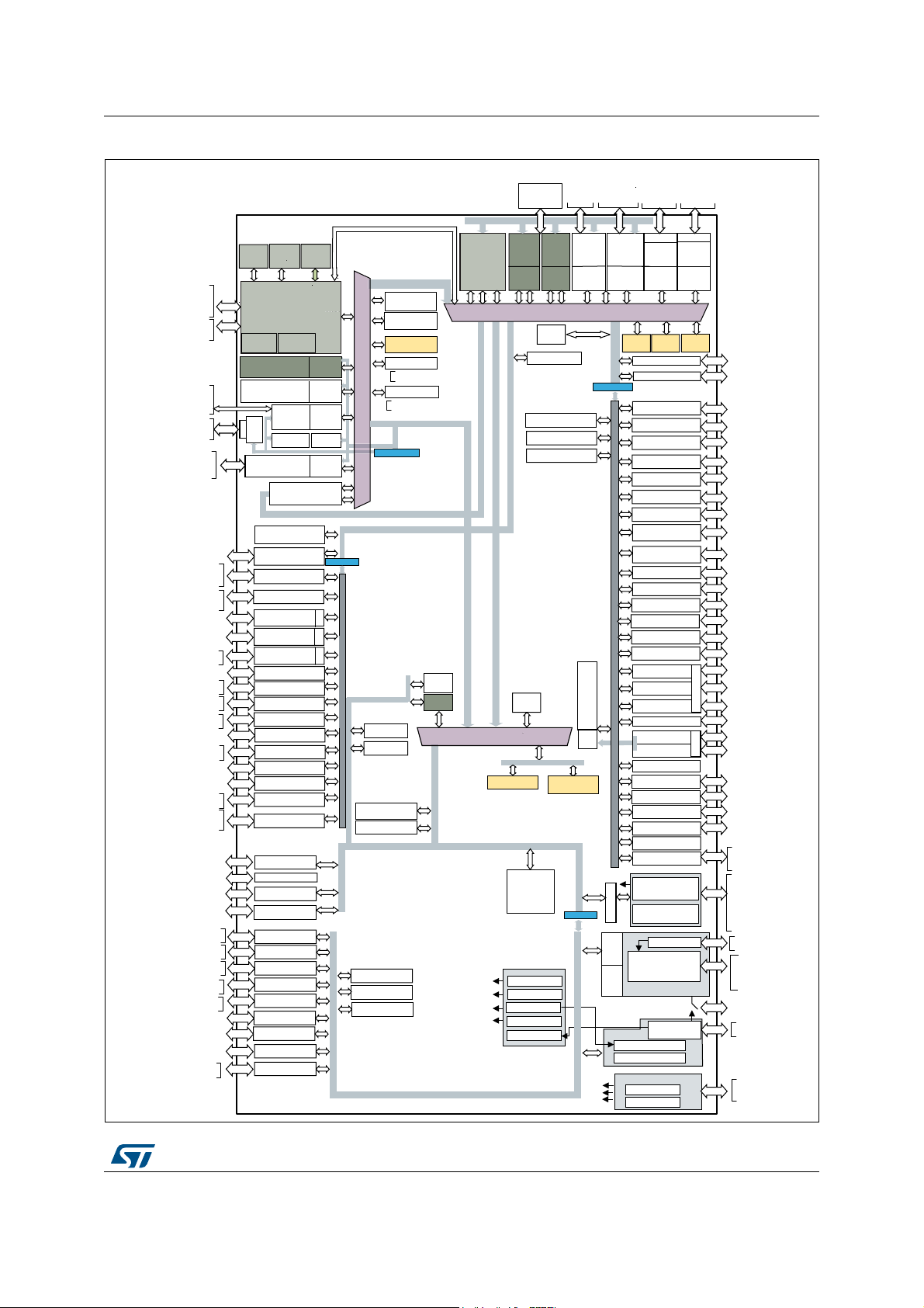
Figure 1 shows the device block diagram.
DS12930 Rev 1 5/242
46
Page 16
Description STM32H747xI/G
Table 1. STM32H747xI/G features and peripheral counts
Peripherals
STM32H747AG
Flash memory in Kbytes 2 x 512 Kbytes 2 x 1 Mbyte
SRAM
mapped onto
AXI bus
SRAM1
(D2 domain)
SRAM in Kbytes
TCM RAM in
Kbytes
Backup SRAM (Kbytes) 4
FMC Yes
SRAM2
(D2 domain)
SRAM3
(D2 domain)
SRAM4
(D3 domain)
ITCM RAM
(instruction)
DTCM RAM
(data)
STM32H747IG
STM32H747BG
STM32H747XG
STM32H747ZI
512
128
128
32
64
64
128
STM32H747AI
STM32H747II
STM32H747BI
STM32H747XI
General-purpose input/outputs 112 119 148 168 99 112 119 148 168
Quad-SPI Yes
Ethernet Yes
High-
resolution
General-
purpose
Timers
Wakeup pins
Tamper pins
Random number generator Yes
6/242 DS12930 Rev 1
Advanced-
control (PWM)
Basic 2
Low-power 5
4
2
6
3
10
1
2
4
2
6
3
Page 17
STM32H747xI/G Description
Table 1. STM32H747xI/G features and peripheral counts (continued)
Peripherals
STM32H747AG
STM32H747IG
STM32H747BG
STM32H747XG
SPI / I2S6/3
I2C4
USART/UART
/LPUART
SAI 4
SPDIFRX 4 inputs
Communication
interfaces
SWPMI Yes
MDIO Yes
SDMMC 2
FDCAN/TT-
FDCAN
USB OTG_FS Yes
USB OTG_HS Yes
Ethernet and camera interface Yes
LCD-TFT Yes
MIPI-DSI Host Yes
4/4
/1
1/1
(1)
STM32H747ZI
STM32H747AI
STM32H747II
STM32H747BI
STM32H747XI
JPEG Codec Yes
Chrom-ART Accelerator™
(DMA2D)
Yes
GPIOs Up to 168
16-bit ADCs
Number of Direct channels
Number of Fast channels
Number of Slow channels
12-bit DAC
Number of channels
17
2
9
2
9
21
4
9
23
3
2
7
14
Yes
2
Comparators 2
Operational amplifiers 2
DFSDM Yes
Maximum CPU frequency 480 MHz
DS12930 Rev 1 7/242
17
2
9
2
9
21
4
9
23
46
Page 18
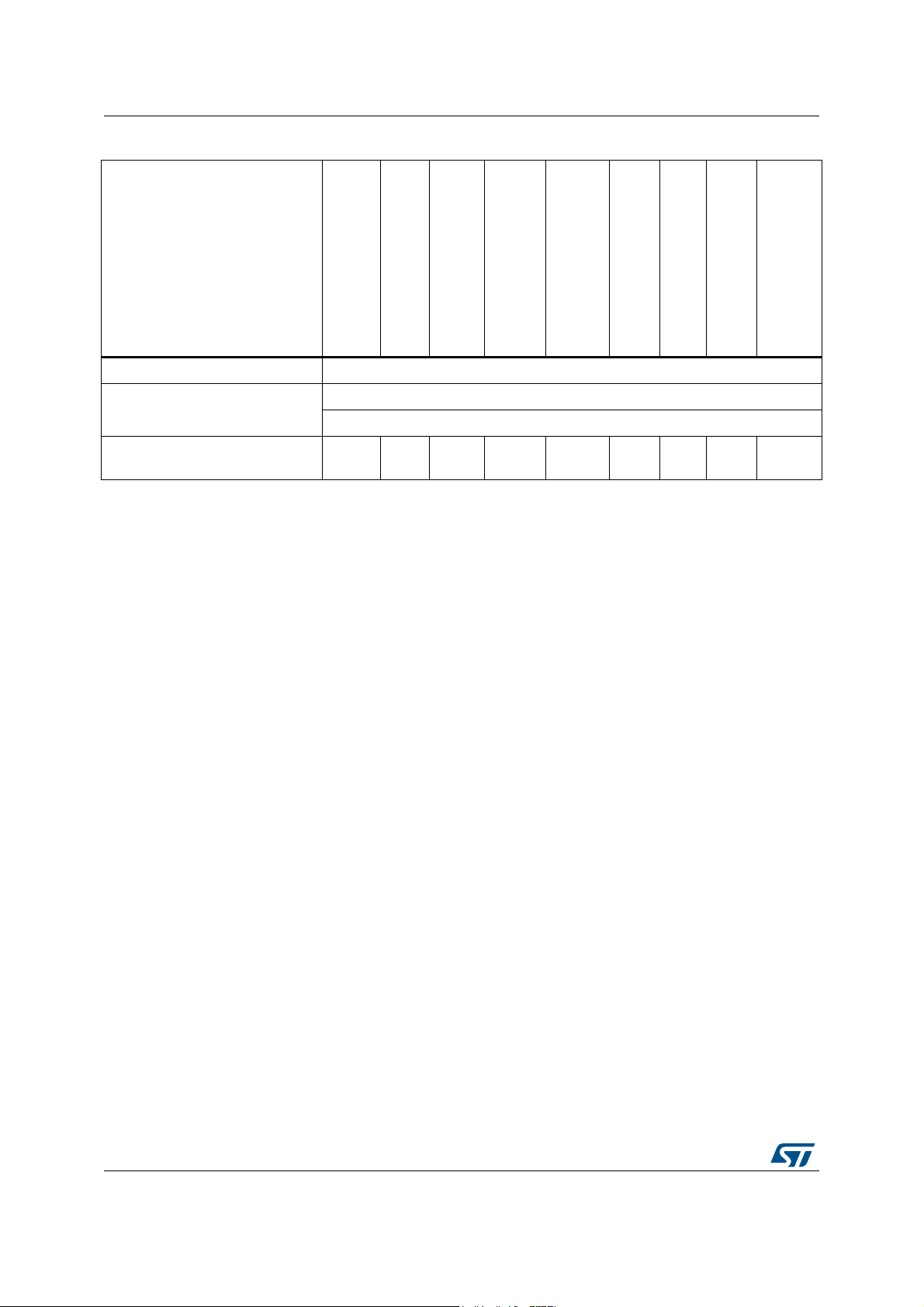
Description STM32H747xI/G
Table 1. STM32H747xI/G features and peripheral counts (continued)
Peripherals
STM32H747AG
STM32H747IG
STM32H747BG
STM32H747XG
STM32H747ZI
Operating voltage 1.62 to 3.6 V
Ambient temperatures: –40 up to +85 °C
STM32H747AI
(2)
STM32H747II
(3)
STM32H747BI
Operating temperatures
Junction temperature: –40 to + 125 °C
Package
1. The SPI1, SPI2 and SPI3 interfaces give the flexibility to work in an exclusive way in either the SPI mode or the I2S audio
mode.
2. V
connecting PDR_ON pin to VSS. Otherwise the supply voltage must stay above 1.71 V with the embedded power voltage
detector enabled.
3. The product junction temperature must be kept within the –40 to +125 °C range.
can drop down to 1.62 V by using an external power supervisor (see Section 3.5.2: Power supply supervisor) and
DD/VDDA
UFBGA
169
LQFP
176
LQFP
208
TFBGA
240+25
WLCSP
156
UFBG
A169
LQFP
176
LQFP
208
TFBGA
240+25
STM32H747XI
8/242 DS12930 Rev 1
Page 19
STM32H747xI/G Description
MSv43739V12
FDCAN1
FDCAN2
I2C1/SMBUS
I2C2/SMBUS
I2C3/SMBUS
AXI/AHB12 (200MHz)
4 compl. chan. (TIM1_CH1[1:4]N),
4 chan. (TIM1_CH1[1:4]ETR, BKIN as AF
APB1 30MHz
TX, RX
SCL, SDA, SMBAL as AF
APB1 100 MHz (max)
MDMA
PK[7:0]
4 compl. chan.(TIM8_CH1[1:4]N),
4 chan. (TIM8_CH1[1:4], ETR, BKIN as
AF
RX, TX, SCK,
CTS, RTS as AF
SCL, SDA, SMBAL as AF
SCL, SDA, SMBAL as AF
MOSI, MISO, SCK, NSS/SDO,
SDI, CK, WS, MCK, as AF
TX, RX
RX, TX as AF
RX, TX as AF
RX, TX, SCK
CTS, RTS as AF
RX, TX, SCK, CTS,
RTS as AF
1 channel as AF
smcard
irDA
1 channel as AF
2 channels as AF
4 channels
4 channels, ETR as AF
4 channels, ETR as AF
4 channels, ETR as AF
RX, TX as AF
FIFO
LCD-TFT
FIFO
CHROM-ART
(DMA2D)
SD, SCK, FS, MCLK as AF
FIFO
LCD_R[7:0], LCD_G[7:0],
LCD_B[7:0], LCD_HSYNC,
LCD_VSYNC, LCD_DE,
LCD_CLK
CLK, CS,D[7:0]
64-bit AXI BUS-MATRIX
CEC as AF
IN[1:4] as AF
MDC, MDIO
AXIM
AHBP
AHBS
TRACECK
TRACED[3:0]
JTRST, JTDI,
JTCK/SWCLK
JTDO/SWD, JTDO
JTAG/SW
ETM
I-Cache
16KB
D-Cache
16KB
ITCM
4KB
D-
TCM
64KB
16 Streams
FIFO
SDMMC1
SDMMC_D[7:0],SDMMC_D[7:3,1]Dir
SDMMC_D0dir, SDMMC_D2dir
CMD, CMDdir, CK, Ckin,
CKio as AF
FIFO
DMA1
FIFOs
8 Stream
DMA2
FIFOs
ETHER
MAC
SDMMC2
FIFO
OTG_HS
FIFO
OTG_FS
FIFO
SRAM1
128 KB
8 Stream
FMC_signals
DMA DMA/ DMA/
PHY PHY
MII / RMII
MDIO
as AF
DP, DM, STP,
NXT,ULPI:CK
, D[7:0], DIR,
ID, VBUS
AHB1 (200MHz)
ADC1
DAC1_OUT, DAC2_OUT as AF
16b
AXI/AHB34 (200MHz)
JPEGWWDG1
AHB2 (200MHz)
AHB2 (200MHz)
PA..J[15:0]
HSYNC, VSYNC, PUIXCLK, D[13:0]
SAI3
MOSI, MISO,
SCK, NSS as AF
MOSI, MISO, SCK, NSS as AF
smcard
irDA
32-bit AHB BUS-MATRIX
32-bit AHB BUS-MATRIX
AHB4 (200MHz)
BDMA
DMA
Mux2
Up to 20 analog inputs
common to ADC1 & 2
HSEM
AHB4 (200MHz)
AHB3
AHB4
AHB4
AHB4
AHB4
AHB4
VDDA, VSSA
NRESET
WKUP[5:0]
@VDD
RCC
Reset &
control
OSC32_IN
OSC32_OUT
VBAT = 1.2 to 3.6 V
AWU
VDD12
LS
LS
OSC_IN
OSC_OUT
RTC_TS
RTC_TAMP[1:3]
RTC_OUT
RTC_REFIN
VDD = 1.62 to 3.6V
VDDUSB33 = 3.0 to 3.6V
VDDDSI = 1.8 to 3.6V
VSS
VCAP
VDDMMC33 = 1.8 to 3.6 V
VDDSMPS, VSSSMPS
VLXSMPS, VFBSMPS
@VDD
@VDD33
@VSW
PWRCTRL
AHB4 (200MHz)
SUPPLY SUPERVISION
Int
POR
reset
@VDD
LPTIM1_IN1, LPTIM1_IN2,
LPTIM1_OUT as AF
OPAMPx_VINM
OPAMPx_VINP
OPAMPx_VOUT as AF
HRTIM1_CH[A..E]x
HRTIM1_FLT[5:1],
HRTIM1_FLT[5:1]_in, SYSFLT
DFSDM1_CKOUT,
DFSDM1_DATAIN[0:7],
DFSDM1_CKIN[0:7]
2 compl. chan.(TIM15_CH1[1:2]N),
2 chan. (TIM_CH15[1:2], BKIN as AF
1 compl. chan.(TIM16_CH1N),
1 chan. (TIM16_CH1, BKIN as AF
1 compl. chan.(TIM17_CH1N),
1 chan. (TIM17_CH1, BKIN as AF
SDMMC_
D[7:0],
CMD, CK as AF
Up to 17 analog inputs
common to ADC1 and 2
SD, SCK, FS, MCLK,
PDM_DI/CK[4:1] as AF
SCL, SDA, SMBAL as AF
COMPx_INP, COMPx_INM,
COMPx_OUT as AF
LPTIM5_OUT as AF
D-
TCM
64KB
AHB/APB
Quad-SPI
Up to 1 MB
FLASH
Up to 1 MB
FLASH
512 KB AXI
SRAM
FMC
Delay block
DCMI
AHB/APB
HRTIM1
DFSDM1
SD, SCK, FS, MCLK as AF
FIFO
SAI2
SD, SCK, FS, MCLK, D[3:1],
CK[2:1] as AF
FIFO
SAI1
SPI5
TIM17
TIM16
TIM15
SPI4
MOSI, MISO, SCK, NSS/
SDO, SDI, CK, WS, MCK, as AF
SPI/I2S1
USART6
RX, TX, SCK,
CTS, RTS as AF
irDA
USART1
TIM1/PWM
16b
TIM8/PWM
16b
APB2 100 MHz (max)
ADC3
GPIO PORTA.. J
GPIO PORTK
SAI4
COMP1&2
LPTIM5
LPTIM4_OUT as AF
LPTIM4
LPTIM3_OUT as AF
LPTIM3
I2C4
MISO, MOSI, SCK, NSS as AF
SPI6
RX, TX, CK, CTS, RTS as AF
LPUART1
LPTIM2
VREF
SYSCFG
EXTI WKUP
CRC
DAP
DMA
Mux1
To APB1-2
peripherals
SRAM2
128 KB
SRAM3
32 KB
ADC2
AHB/APB
TIM6
16b
TIM7
16b
SWPMI
TIM2
32b
TIM3
16b
TIM4
16b
TIM5
32b
TIM12
16b
TIM13
16b
TIM14
16b
USART2
smcard
irDA
USART3
UART4
UART5
UART7
RX, TX as AF
UART8
SPI2/I2S2
MOSI, MISO, SCK, NSS/SDO,
SDI, CK, WS, MCK, as AF
SPI3/I2S3
Digital filter
MDIOS
FIFO
10 KB SRAM
RAM
I/F
CRS
SPDIFRX1
HDMI-CEC
DAC1&2
LPTIM1
OPAMP1&2
AHB/APB
XTAL 32 kHz
RTC
Backup registers
XTAL OSC
4- 48 MHz
32 KHz LSI RC
PLL1+PLL2+PLL3
POR/PDR/BOR
PVD
smcard
LSI
HSI
CSI
RC48
LPTIM2_OUT as AF
AHB1 (200MHz)
DP, DM, ID,
VBUS
64 KB SRAM
4 KB BKP
RAM
AHB4
ARM
Cortex
M4
Arm
Cortex
M7
I-
Bus
D-
Bus
S-
Bus
D
S
I
DSI_D0_P, DSI_D0_N
DSI_D1_P, DSI_D1_N
DSI_CK_P, DSI_CK_N
PHY
ART
(instruction cache)
AHB ART (200MHz)
AHB ART(200MHz)
RNG
WWDG2
IWDG1
IWDG2
Voltage regulator
3.3 to 1.2V
SMPS step-down
converter
4 MHz CSI
48 MHz HSI48 RC
64 MHz HSI RC
APB4 100 MHz (max)
APB4 100 MHz (max)
IWDG1
IWDG2
VDDREF_ADC
Tem. sensor
Figure 1. STM32H747xI/G block diagram
XI
DS12930 Rev 1 9/242
46
Page 20
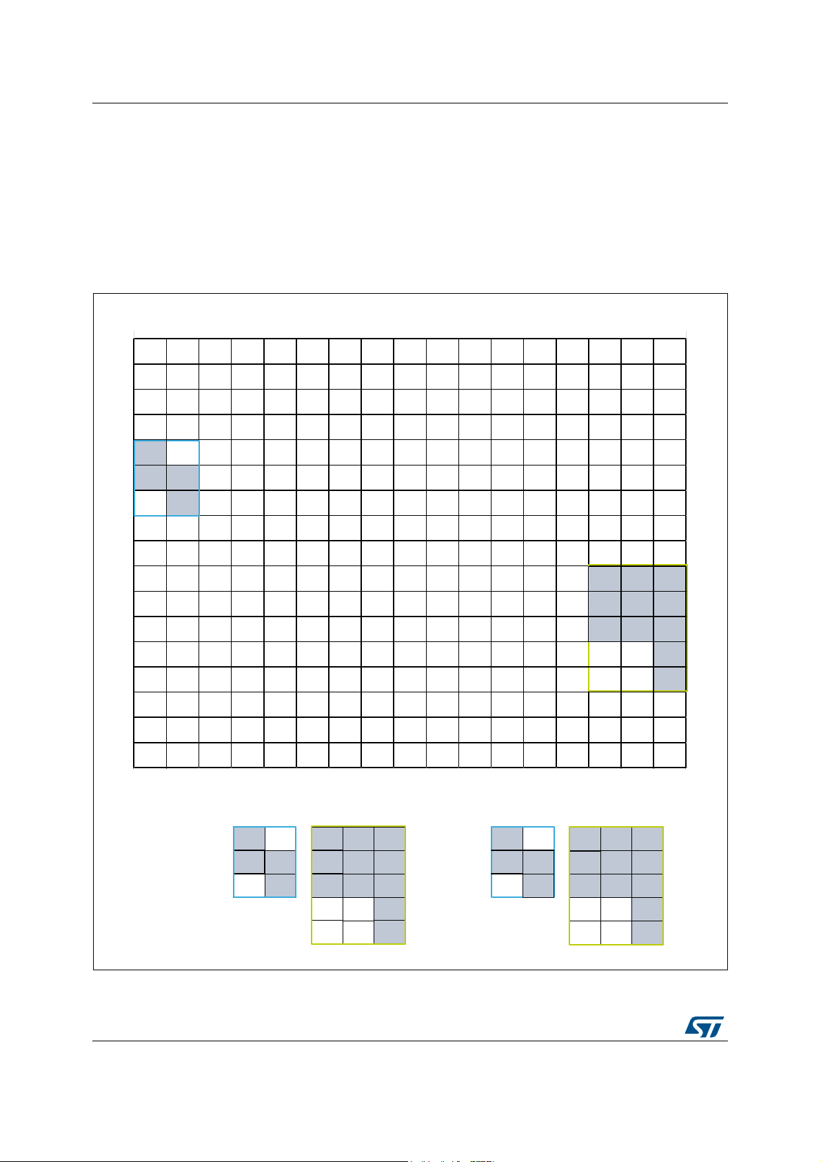
Description STM32H747xI/G
MSv48802V2
VDD
SMPS
STM32H7x7 STM32H7x3
VLX
SMPS
VSS
SMPS
VFB
SMPS
NC
PI9
PF2
NC
NC
NC
12345678910 111213 14151617
A
VSS PI6 PI5 PI4 PB5 VDDLDO
VCAP
PK5 PG10 PG9 PD5 PD4 PC10 PA15 PI1 PI0 VSS
B
VBAT VSS PI7 PE1 PB6 VSS PB4 PK4 PG11 PJ15 PD6 PD3 PC11 PA14 PI2 PH15 PH14
C
PC15-
OSC32_
OUT
PC14-
OSC32_
IN
PE2 PE0 PB7 PB3 PK6 PK3 PG12 VSS PD7 PC12 VSS PI3 PA13 VSS VDDLDO
D
PE5 PE4 PE3 PB9 PB8 PG15 PK7 PG14 PG13 PJ14 PJ12 PD2 PD0 PA10 PA9 PH13
VCAP
E
PI9 PC13 PI8 PE6 VDD
PDR
_ON
BOOT0 VDD PJ13 VDD PD1 PC8 PC9 PA8 PA12 PA11
F
PI10 PI11 VDD PC7 PC6 PG8 PG7
VDD33
USB
G
PF2 PF1 PF0 VDD VSS VSS VSS VSS VSS VDD PG5 PG6 VSS
VDD5
USB
H
PI12 PI13 PI14 PF3 VDD VSS VSS VSS VSS VSS VDD PG4 PG3 PG2 PK2
J
PH1-
OSC_
OUT
PH0-
OSC_
IN
VSS PF5 PF4 VSS VSS VSS VSS VSS VDD PK0 PK1
VSS
DSI
VSSDSI
K
NRST PF6 PF7 PF8 VDD VSS VSS VSS VSS VSS VDD PJ11
L
VDDA PC0 PF10 PF9 VDD VSS VSS VSS VSS VSS VDD PJ10
M
VREF+ PC1 PC2 PC3 VDD VDD PJ9
N
VREF- PH2 PA2 PA1 PA0 PJ0 VDD VDD PE10 VDD VDD VDD PJ8 PJ7 PJ6 VSS
P
VSSA PH3 PH4 PH5 PI15 PJ1 PF13 PF14 PE9 PE11 PB10 PB11 PH10 PH11 PD15 PD14
R
PC2_C PC3_C PA6 VSS PA7 PB2 PF12 VSS PF15 PE12 PE15 PJ5 PH9 PH12 PD11 PD12 PD13
T
PA0_C PA1_C PA5 PC4 PB1 PJ2 PF11 PG0 PE8 PE13 PH6 VSS PH8 PB12 PB15 PD10 PD9
U
VSS PA3 PA4 PC5 PB0 PJ3 PJ4 PG1 PE7 PE14
VCAP
VDDLDO
PH7 PB13 PB14 PD8 VSS
VSSDSI
PI9
PF2
VSSDSI
DSI_CKP
DSI_CKN
DSI_D0N
DSI_D1P
DSI_D1N
VSS
VDDCAP
DSI
PJ6
PD14
VDDDSI
PD15
PI9
PF2 VSSDSI DSI_D0P
VSS
PI9
PF2
VSS
NC
NC
NC
NC
NC
VSS
NC
PJ6
PD14
VDD
PD15
VSS NC
Compatibility throughout the family
STM32H747xI/G devices are not pin-to-pin compatible with STM32H7x3 devices (single
core line):
• The TFBGA240+25 ballout is compatible with STM32H7x3 devices, except for a few
I/O balls as shown in Figure 2.
• LQFP208 and LQFP176 pinouts, as well as UFBGA176+25 ballout are not compatible
with STM32H7x3 devices.
Figure 2. TFBGA240+25 ball assignment differences
1. The balls highlighted in gray correspond to different signals on STM32H747xI/G and STM32H7x3 devices.
10/242 DS12930 Rev 1
Page 21

STM32H747xI/G Functional overview
3 Functional overview
3.1 Dual Arm
The dual-core MIPI-DSI STM32H747xI/G devices embed two Arm® cores, a Cortex®-M7
and a Cortex
while the Cortex
The two cores belong to separate power domains. This allows designing gradual highpower efficiency solutions in combination with the low-power modes already available on all
STM32 microcontrollers.
®
Cortex
®
-M4. The Cortex®-M4 offers optimal performance for real-time applications
®
®
cores
-M7 core can execute high-performance tasks in parallel.
3.1.1 Arm® Cortex®-M7 with FPU
The Arm® Cortex®-M7 with double-precision FPU processor is the latest generation of Arm
processors for embedded systems. It was developed to provide a low-cost platform that
meets the needs of MCU implementation, with a reduced pin count and optimized power
consumption, while delivering outstanding computational performance and low interrupt
latency.
The Cortex®-M7 processor is a highly efficient high-performance featuring:
• Six-stage dual-issue pipeline
• Dynamic branch prediction
• Harvard architecture with L1 caches (16 Kbytes of I-cache and 16 Kbytes of D-cache)
• 64-bit AXI interface
• 64-bit ITCM interface
• 2x32-bit DTCM interfaces
The following memory interfaces are supported:
• Separate Instruction and Data buses (Harvard Architecture) to optimize CPU latency
• Tightly Coupled Memory (TCM) interface designed for fast and deterministic SRAM
accesses
• AXI Bus interface to optimize Burst transfers
• Dedicated low-latency AHB-Lite peripheral bus (AHBP) to connect to peripherals.
The processor supports a set of DSP instructions which allow efficient signal processing and
complex algorithm execution.
It also supports single and double precision FPU (floating point unit) speeds up software
development by using metalanguage development tools, while avoiding saturation.
Figure 1 shows the general block diagram of the STM32H747xI/G family.
Note: Cortex®-M7 with FPU core is binary compatible with the Cortex®-M4 core.
DS12930 Rev 1 11/242
46
Page 22

Functional overview STM32H747xI/G
3.1.2 Arm® Cortex®-M4 with FPU
The Arm® Cortex®-M4 processor is a high-performance embedded processor which
supports DSP instructions. It was developed to provide an optimized power consumption
MCU, while delivering outstanding computational performance and low interrupt latency.
The Arm® Cortex®-M4 processor is a highly efficient MCU featuring:
• 3-stage pipeline with branch prediction
• Harvard architecture
• 32-bit System (S-BUS) interface
• 32-bit I-BUS interface
• 32-bit D-BUS interface
The Arm® Cortex®-M4 processor also features a dedicated hardware adaptive real-time
accelerator (ART Accelerator
four 256-bit lines, a 256-bit cache buffer connected to the 64-bit AXI interface and a 32-bit
interface for non-cacheable accesses.
™
). This is an instruction cache memory composed of sixty-
3.2 Memory protection unit (MPU)
The devices feature two memory protection units. Each MPU manages the CPU access
rights and the attributes of the system resources. It has to be programmed and enabled
before use. Its main purposes are to prevent an untrusted user program to accidentally
corrupt data used by the OS and/or by a privileged task, but also to protect data processes
or read-protect memory regions.
The MPU defines access rules for privileged accesses and user program accesses. It
allows defining up to 16 protected regions that can in turn be divided into up to 8
independent subregions, where region address, size, and attributes can be configured. The
protection area ranges from 32 bytes to 4
When an unauthorized access is performed, a memory management exception is
generated.
Gbytes of addressable memory.
12/242 DS12930 Rev 1
Page 23

STM32H747xI/G Functional overview
3.3 Memories
3.3.1 Embedded Flash memory
The STM32H747xI/G devices embed up to 2 Mbytes of Flash memory that can be used for
storing programs and data.
The Flash memory is organized as 266-bit Flash words memory that can be used for storing
both code and data constants. Each word consists of:
• One Flash word (8 words, 32 bytes or 256 bits)
• 10 ECC bits.
The Flash memory is divided into two independent banks. Each bank is organized as
follows:
• A user Flash memory block of 512 Kbytes (STM32H7xxxG) or 1-Mbyte (STM32H7xxxI)
containing eight user sectors of 128 Kbytes (4 K Flash memory words)
• 128 Kbytes of System Flash memory from which the device can boot
• 2 Kbytes (64 Flash words) of user option bytes for user configuration
3.3.2 Embedded SRAM
All devices feature around 1 Mbyte of RAM with hardware ECC. The RAM is divided as
follows:
• 512 Kbytes of AXI-SRAM mapped onto AXI bus on D1 domain.
• SRAM1 mapped on D2 domain: 128 Kbytes
• SRAM2 mapped on D2 domain: 128 Kbytes
• SRAM3 mapped on D2 domain: 32 Kbytes
• SRAM4 mapped on D3 domain: 64 Kbytes
• 4 Kbytes of backup SRAM
The content of this area is protected against possible unwanted write accesses,
and is retained in Standby or V
• RAM mapped to TCM interface (ITCM and DTCM):
Both ITCM and DTCM RAMs are 0 wait state memories. They can be accessed either
from the Arm
AHB slave of the Cortex
®
Cortex®-M7 CPU or the MDMA (even in Sleep mode) through a specific
®
-M7(AHBS):
– 64 Kbytes of ITCM-RAM (instruction RAM)
This RAM is connected to ITCM 64-bit interface designed for execution of critical
real-times routines by the Cortex
– 128 Kbytes of DTCM-RAM (2x 64-Kbyte DTCM-RAMs on 2x32-bit DTCM ports)
The DTCM-RAM could be used for critical real-time data, such as interrupt service
routines or stack/heap memory. Both DTCM-RAMs can be used in parallel (for
load/store operations) thanks to the Cortex
The MDMA can be used to load code or data in ITCM or DTCM RAMs.
BAT
mode.
®
-M7.
®
-M7 dual issue capability.
DS12930 Rev 1 13/242
46
Page 24

Functional overview STM32H747xI/G
Error code correction (ECC)
Over the product lifetime, and/or due to external events such as radiations, invalid bits in
memories may occur. They can be detected and corrected by ECC. This is an expected
behavior that has to be managed at final-application software level in order to ensure data
integrity through ECC algorithms implementation.
SRAM data are protected by ECC:
• 7 ECC bits are added per 32-bit word.
• 8 ECC bits are added per 64-bit word for AXI-SRAM and ITCM-RAM.
The ECC mechanism is based on the SECDED algorithm. It supports single-error correction
and double-error detection.
3.3.3 ART™ accelerator
The ART™ (adaptive real-time) accelerator block speeds up instruction fetch accesses of
the Cortex
®
-M4 core from D1-domain internal memories (Flash memory bank 1, Flash
memory bank 2, AXI SRAM) and from D1-domain external memories attached via QuadSPI controller and Flexible memory controller (FMC).
The ART™ accelerator is a 256-bit cache line using 64-bit WRAP4 accesses from the 64-bit
AXI D1 domain. The acceleration is achieved by loading selected code into an embedded
cache and making it instantly available to Cortex
®
-M4 core, thus avoiding latency due to
memory wait states.
Figure 3. shows the block schematic and the environment of the ART accelerator.
14/242 DS12930 Rev 1
Page 25
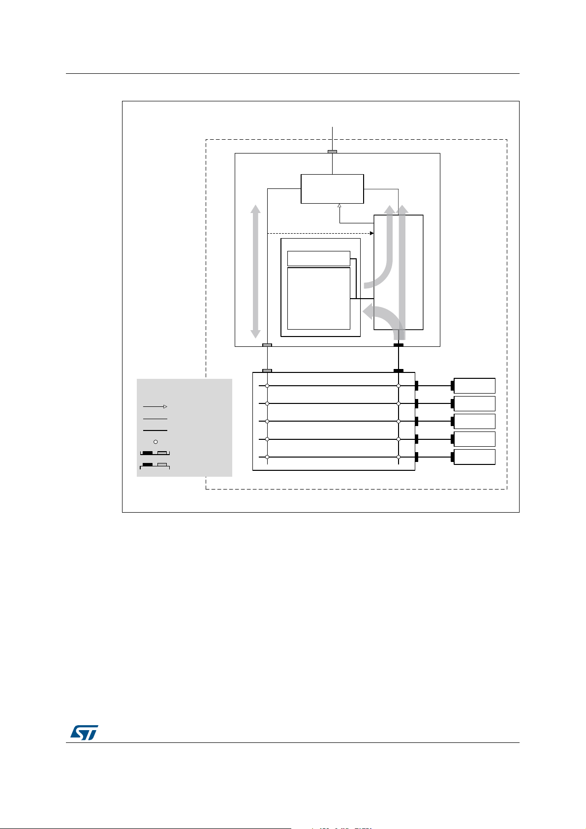
STM32H747xI/G Functional overview
MSv39757V2
64-bit AXI bus matrix
Flash bank 1
Flash bank 2
AXI SRAM
QSPI
FMC
AHB from D2 domain
32-bit bus
64-bit bus
Bus multiplexer
Legend
Master interface
Slave interface
AXI AHB
ART accelerator
AHB switch
Non-cacheable
access path
Cacheable
access path
AXI access
AHB access
D1 domain
Control
control
Cache memory
64 x 256-bit
Cache memory
64 x 256-bit
Cache buffer
1 x 256-bit
Cache
non-
cacheable
access
Detect of
write to cacheable page
instruction
fetch
cache
hit
cache
miss
cache
refill
Cache
manager
Figure 3. ART™ accelerator schematic and environment
3.4 Boot modes
By default, the boot codes are executed simultaneously by both cores. However, by
programming the appropriate Flash user option byte, it is possible to boot from one core
while clock-gating the other core.
At startup, the boot memory space is selected by the BOOT pin and BOOT_ADDx option
bytes, allowing to program any boot memory address from 0x0000 0000 to 0x3FFF FFFF
which includes:
• All Flash address space
• Flash memory and SRAMs (except for ITCM /DTCM RAMs which cannot be accessed
by the Cortex
®
-M4 core)
DS12930 Rev 1 15/242
46
Page 26

Functional overview STM32H747xI/G
The bootloader is located in non-user System memory. It is used to reprogram the Flash
memory through a serial interface (USART, I2C, SPI, USB-DFU). Refer to STM32
microcontroller System memory Boot mode application note (AN2606) for details.
3.5 Power supply management
3.5.1 Power supply scheme
STM32H747xI/G power supply voltages are the following:
• V
= 1.62 to 3.6 V: external power supply for I/Os, provided externally through V
DD
pins.
• V
• V
= 1.62 to 3.6 V: supply voltage for the internal regulator supplying V
DDLDO
= 1.62 to 3.6 V: external analog power supplies for ADC, DAC, COMP and
DDA
CORE
OPAMP.
• V
DD33USB and VDD50USB
V
DD50USB
can be supplied through the USB cable to generate the V
USB internal regulator. This allows supporting a V
The USB regulator can be bypassed to supply directly V
• V
• V
= 1.2 to 3.6 V: power supply for the VSW domain when VDD is not present.
BAT
CAP
: V
supply voltage, which values depend on voltage scaling (1.0 V, 1.1 V,
CORE
:
supply different from 3.3 V.
DD
DD33USB
DD33USB
if VDD = 3.3 V.
via the
1.2 V or 1.35 V). They are configured through VOS bits in PWR_D3CR register and
ODEN bit in the SYSCFG_PWRCR register. The V
domain is split into the
CORE
following power domains that can be independently switch off.
– D1 domain containing some peripherals and the Cortex
– D2 domain containing a large part of the peripherals and the Cortex
®
-M7 core.
®
-M4 core.
– D3 domain containing some peripherals and the system control.
• V
• V
• V
DDSMPS
V
DDSMPS
LXSMPS
FBSMPS
= 1.62 V to 3.6 V: SMPS step-down converter power supply
must be kept at the same voltage level as VDD.
= SMPS step-down converter output coupled to an inductor.
= V
, 1.8 V or 2.5 V external SMPS step-down converter feedback
CORE
voltage sense input.
• V
• V
• V
= 1.62 to 3.6 V: supply voltage for the DSI internal regulator
DDDSI
DD12DSI
CAPDSI
= 1.15 to 1.3 V: optional supply voltage for the DSI PHY (DSI regulator off)
: DSI regulator supply output
During power-up and power-down phases, the following power sequence requirements
must be respected (see
• When VDD is below 1 V, other power supplies (V
must remain below V
• When V
is above 1 V, all power supplies are independent (except for V
DD
which must remain at the same level as V
Figure 4):
+ 300 mV.
DD
DD
).
DDA
, V
DD33USB
, V
DD50USB
, V
DDDSI
DDSMPS
During the power-down phase, VDD can temporarily become lower than other supplies only
if the energy provided to the microcontroller remains below 1
mJ. This allows external
decoupling capacitors to be discharged with different time constants during the power-down
transient phase.
DD
,
)
16/242 DS12930 Rev 1
Page 27
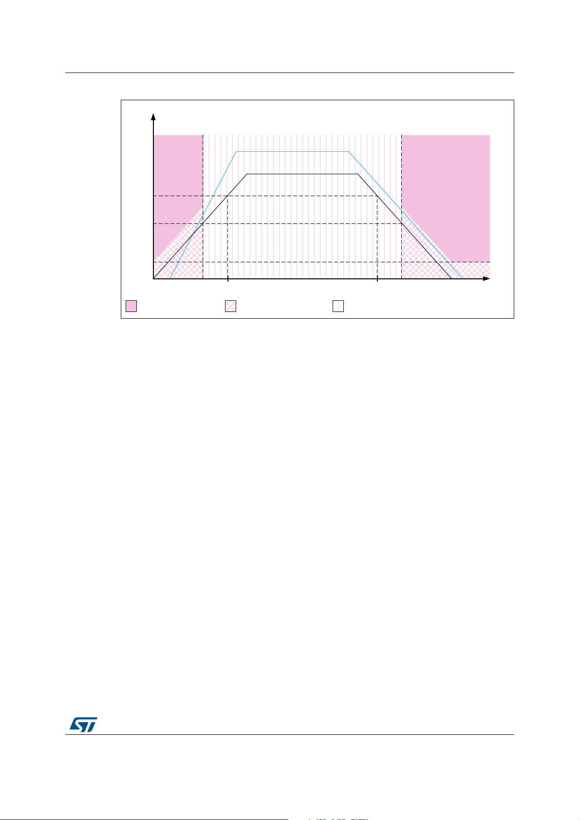
STM32H747xI/G Functional overview
MSv47490V1
0.3
1
V
BOR0
3.6
Operating modePower-on Power-down time
V
V
DDX
(1)
V
DD
Invalid supply area V
DDX
< V
DD
+ 300 mV
V
DDX
independent from V
DD
Figure 4. Power-up/power-down sequence
1. V
2. V
refers to any power supply among V
DDx
DD
and V
must be wired together into order to follow the same voltage sequence.
DDSMPS
3.5.2 Power supply supervisor
The devices have an integrated power-on reset (POR)/ power-down reset (PDR) circuitry
coupled with a Brownout reset (BOR) circuitry:
• Power-on reset (POR)
The POR supervisor monitors V
The devices remain in Reset mode when V
• Power-down reset (PDR)
The PDR supervisor monitors V
below a fixed threshold.
The PDR supervisor can be enabled/disabled through PDR_ON pin.
• Brownout reset (BOR)
The BOR supervisor monitors V
2.7 V) can be configured through option bytes. A reset is generated when V
below this threshold.
, V
DDA
power supply and compares it to a fixed threshold.
DD
power supply. A reset is generated when V
DD
power supply. Three BOR thresholds (from 2.1 to
DD
DD33USB
, V
DD50USB
is below this threshold,
DD
and V
DDDSI
.
DD
DD
drops
drops
DS12930 Rev 1 17/242
46
Page 28

Functional overview STM32H747xI/G
3.5.3 Voltage regulator (SMPS step-down converter and LDO)
The same voltage regulator supplies the 3 power domains (D1, D2 and D3). D1 and D2 can
be independently switched off.
Voltage regulator output can be adjusted according to application needs through 6 power
supply levels:
• Run mode (VOS0 to VOS3)
– Scale 0: boosted performance (available only with LDO regulator)
– Scale 1: high performance
– Scale 2: medium performance and consumption
– Scale 3: optimized performance and low-power consumption
Note: For STM32H7x7xIT3 sales types (industrial temperature range) the voltage regulator output
can be set only to VOS2 or VOS3 in Run mode (VOS1 is not available for industrial
temperature range).
• Stop mode (SVOS3 to SVOS5)
– Scale 3: peripheral with wakeup from Stop mode capabilities (UART, SPI, I2C,
LPTIM) are operational
– Scale 4 and 5 where the peripheral with wakeup from Stop mode is disabled
The peripheral functionality is disabled but wakeup from Stop mode is possible
through GPIO or asynchronous interrupt
.
3.5.4 SMPS step-down converter
The built-in SMPS step-down converter is a highly power-efficient DC/DC non-linear
switching regulator that provides lower power consumption than a conventional voltage
regulator (LDO).
18/242 DS12930 Rev 1
Page 29

STM32H747xI/G Functional overview
The SMPS step-down converter can be used for the following purposes:
• Direct supply of the V
CORE
domain
– the SMPS step-down converter operating modes follow the device system
operating modes (Run, Stop, Standby).
– the SMPS step-down converter output voltage are set according to the selected
VOS and SVOS bits (voltage scaling)
• Delivery of an intermediate voltage level to supply the internal voltage regulator (LDO)
– SMPS step-down converter operating modes
When the SDEXTHP bit is equal to 0 in the PWR_CR3 register, the SMPS stepdown converter follows the device system operating modes (Run, Stop and
Standby).
When the SDEXTHP bit is equal to 1 in PWR_CR3, the SMPS step-down
converter is forced to High-performance mode and does not follow the device
system operating modes (Run, Stop and Standby).
– The SMPS step-down converter output equals 1.8 V or 2.5 V according to the
selected SD level
• Delivery of an external supply
– The SMPS step-down converter is forced to High-performance mode (provided
SDEXTHP bit is equal to 1 in PWR_CR3)
– The SMPS step-down converter output equals 1.8 V or 2.5 V according to the
selected SD level
3.6 Low-power strategy
There are several ways to reduce power consumption on STM32H747xI/G:
• Select the SMPS step-down converter as V
enhance power efficiency.
• Select the adequate voltage scaling
• Decrease the dynamic power consumption by slowing down the system clocks even in
Run mode, and by individually clock gating the peripherals that are not used.
• Save power consumption when one or both CPUs are idle, by selecting among the
available low-power mode according to the user application needs. This allows
achieving the best compromise between short startup time, low-power consumption, as
well as available wakeup sources.
The devices feature several low-power modes:
• CSleep (CPU clock stopped)
• CStop (CPU sub-system clock stopped)
• DStop (Domain bus matrix clock stopped)
• Stop (System clock stopped)
• DStandby (Domain powered down)
• Standby (System powered down)
CSleep and CStop low-power modes are entered by the MCU when executing the WFI
(Wait for Interrupt) or WFE (Wait for Event) instructions, or when the SLEEPONEXIT bit of
the Cortex
®
-Mx core is set after returning from an interrupt service routine.
supply voltage source, as it allows to
CORE
DS12930 Rev 1 19/242
46
Page 30
Functional overview STM32H747xI/G
A domain can enter low-power mode (DStop or DStandby) when the processor, its
subsystem and the peripherals allocated in the domain enter low-power mode. For instance
D1 or D2 domain enters DStop/DStandby mode when the CPU of the domain is in CStop
mode AND the other CPU has no peripheral allocated in that domain, or if it is in CStop
mode too. D3 domain can enter DStop/DStandby mode if both core subsystems do not have
active peripherals in D3 domain, and D3 is not forced in Run mode.
If part of the domain is not in low-power mode, the domain remains in the current mode.
Finally the system can enter Stop or Standby when all EXTI wakeup sources are cleared
and the power domains are in DStop or DStandby mode.
The clock system can be re-initialize by a master CPU (either the Cortex®-M4 or -M7) after
exiting Stop mode while the slave CPU is held in low-power mode. Once the master CPU
has re-initialized the system, the slave CPU can receive a wakeup interrupt and proceed
with the interrupt service routine.
Table 2. System vs domain low-power mode
System power mode
Run DRun/DStop/DStandby DRun/DStop/DStandby DRun
Stop DStop/DStandby DStop/DStandby DStop
Standby DStandby DStandby DStandby
D1 domain power
mode
3.7 Reset and clock controller (RCC)
The clock and reset controller is located in D3 domain. The RCC manages the generation of
all the clocks, as well as the clock gating and the control of the system and peripheral
resets. It provides a high flexibility in the choice of clock sources and allows to apply clock
ratios to improve the power consumption. In addition, on some communication peripherals
that are capable to work with two different clock domains (either a bus interface clock or a
kernel peripheral clock), the system frequency can be changed without modifying the
baudrate.
3.7.1 Clock management
The devices embed four internal oscillators, two oscillators with external crystal or
resonator, two internal oscillators with fast startup time and three PLLs.
The RCC receives the following clock source inputs:
• Internal oscillators:
– 64 MHz HSI clock
– 48 MHz RC oscillator
– 4 MHz CSI clock
– 32 kHz LSI clock
• External oscillators:
– HSE clock: 4-50 MHz (generated from an external source) or 4-48 MHz(generated
from a crystal/ceramic resonator)
– LSE clock: 32.768 kHz
D2 domain power
mode
D3 domain power
mode
20/242 DS12930 Rev 1
Page 31

STM32H747xI/G Functional overview
The RCC provides three PLLs: one for system clock, two for kernel clocks.
The system starts on the HSI clock. The user application can then select the clock
configuration.
3.7.2 System reset sources
Power-on reset initializes all registers while system reset reinitializes the system except for
the debug, part of the RCC and power controller status registers, as well as the backup
power domain.
A system reset is generated in the following cases:
• Power-on reset (pwr_por_rst)
• Brownout reset
• Low level on NRST pin (external reset)
• Independent watchdog 1 (from D1 domain)
• Independent watchdog 2 (from D2 domain)
• Window watchdog 1 (from D1 domain)
• Window watchdog 2 (from D2 domain)
• Software reset
• Low-power mode security reset
• Exit from Standby
3.8 General-purpose input/outputs (GPIOs)
Each of the GPIO pins can be configured by software as output (push-pull or open-drain,
with or without pull-up or pull-down), as input (floating, with or without pull-up or pull-down)
or as peripheral alternate function. Most of the GPIO pins are shared with digital or analog
alternate functions. All GPIOs are high-current-capable and have speed selection to better
manage internal noise, power consumption and electromagnetic emission.
After reset, all GPIOs (except debug pins) are in Analog mode to reduce power
consumption (refer to GPIOs register reset values in the device reference manual).
The I/O configuration can be locked if needed by following a specific sequence in order to
avoid spurious writing to the I/Os registers.
3.9 Bus-interconnect matrix
The devices feature an AXI bus matrix, two AHB bus matrices and bus bridges that allow
interconnecting bus masters with bus slaves (see
Figure 5).
DS12930 Rev 1 21/242
46
Page 32

22/242 DS12930 Rev 1
MSv39740V3
AXIM
DMA2
Ethernet
MAC
SDMMC2DMA1 USBHS1 USBHS2
Cortex-M4
APB1
ART SDMMC1 MDMA DMA2D LTDC
BDMA
APB4
Cortex-M7
I$
16KBD$16KB
AHBP
DMA1_MEM
DMA1_PERIPH
DMA2_MEM
DMA2_PERIPH
S-bus
D-bus
I-bus
APB3
32-bit AHB bus matrix
D2 domain
64-bit AXI bus matrix
D1 domain
32-bit AHB bus matrix
D3 domain
DTCM
128 Kbyte
ITCM
64 Kbyte
Flash A
Up to 1 Mbyte
Flash B
Up to 1 Mbyte
AXI SRAM
512 Kbyte
QSPI
FMC
SRAM1 128
Kbyte
SRAM2 128
Kbyte
SRAM3
32 Kbyte
AHB1
AHB2
AHB4
SRAM4
64 Kbyte
Backup
SRAM
4 Kbyte
AHBS
CPU
CPU
D2-to-D1 AHB
D2-to-D3 AHB
D1-to-D2 AHB
D1-to-D3 AHB
32-bit bus
64-bit bus
Bus multiplexer
Legend
Master interface
1
2
3
Slave interface
AHB3
AXI
AHB
APB
APB2
TCM
7
5
4
6
Figure 5. STM32H747xI/G bus matrix
Functional overview STM32H747xI/G
Page 33

STM32H747xI/G Functional overview
3.10 DMA controllers
The devices feature four DMA instances to unload CPU activity:
• A master direct memory access (MDMA)
The MDMA is a high-speed DMA controller, which is in charge of all types of memory
transfers (peripheral to memory, memory to memory, memory to peripheral), without
any CPU action. It features a master AXI interface and a dedicated AHB interface to
access Cortex
The MDMA is located in D1 domain. It is able to interface with the other DMA
controllers located in D2 domain to extend the standard DMA capabilities, or can
manage peripheral DMA requests directly.
Each of the 16 channels can perform single block transfers, repeated block transfers
and linked list transfers.
• Two dual-port DMAs (DMA1, DMA2) located in D2 domain, with FIFO and request
router capabilities.
• One basic DMA (BDMA) located in D3 domain, with request router capabilities.
The DMA request router could be considered as an extension of the DMA controller. It
routes the DMA peripheral requests to the DMA controller itself. This allowing managing the
DMA requests with a high flexibility, maximizing the number of DMA requests that run
concurrently, as well as generating DMA requests from peripheral output trigger or DMA
event.
®
-M7 TCM memories.
3.11 Chrom-ART Accelerator™ (DMA2D)
The Chrom-Art Accelerator™ (DMA2D) is a graphical accelerator which offers advanced bit
blitting, row data copy and pixel format conversion. It supports the following functions:
• Rectangle filling with a fixed color
• Rectangle copy
• Rectangle copy with pixel format conversion
• Rectangle composition with blending and pixel format conversion
Various image format coding are supported, from indirect 4bpp color mode up to 32bpp
direct color. It embeds dedicated memory to store color lookup tables. The DMA2D also
supports block based YCbCr to handle JPEG decoder output.
An interrupt can be generated when an operation is complete or at a programmed
watermark.
All the operations are fully automatized and are running independently from the CPU or the
DMAs.
DS12930 Rev 1 23/242
46
Page 34

Functional overview STM32H747xI/G
3.12 Nested vectored interrupt controller (NVIC)
Both Cortex®-M7 (CPU1) and Cortex®-M4 (CPU2) cores have their own nested vector
interrupt controller (respectively NVIC1 and NVIC2). Each NVIC instance is able to manage
16 priority levels, and handle up to 150 maskable interrupt channels plus the 16 interrupt
lines of the Cortex
• Closely coupled NVIC gives low-latency interrupt processing
• Interrupt entry vector table address passed directly to the core
• Allows early processing of interrupts
• Processing of late arriving, higher-priority interrupts
• Support tail chaining
• Processor context automatically saved on interrupt entry, and restored on interrupt exit
with no instruction overhead
This hardware block provides flexible interrupt management features with minimum interrupt
latency.
®
-M7 with FPU core.
3.13 Extended interrupt and event controller (EXTI)
The EXTI controller performs interrupt and event management. In addition, it can wake up
the processors, power domains and/or D3 domain from Stop mode.
The EXTI handles up to 89 independent event/interrupt lines split as 28 configurable events
and 61 direct events (including two interrupt lines for inter-core management).
Configurable events have dedicated pending flags, active edge selection, and software
trigger capable.
Direct events provide interrupts or events from peripherals having a status flag.
3.14 Cyclic redundancy check calculation unit (CRC)
The CRC (cyclic redundancy check) calculation unit is used to get a CRC code using a
programmable polynomial.
Among other applications, CRC-based techniques are used to verify data transmission or
storage integrity. In the scope of the EN/IEC 60335-1 standard, they offer a means of
verifying the Flash memory integrity. The CRC calculation unit helps compute a signature of
the software during runtime, to be compared with a reference signature generated at linktime and stored at a given memory location.
24/242 DS12930 Rev 1
Page 35

STM32H747xI/G Functional overview
3.15 Flexible memory controller (FMC)
The FMC controller main features are the following:
• Interface with static-memory mapped devices including:
– Static random access memory (SRAM)
– NOR Flash memory/OneNAND Flash memory
– PSRAM (4 memory banks)
– NAND Flash memory with ECC hardware to check up to 8 Kbytes of data
• Interface with synchronous DRAM (SDRAM/Mobile LPSDR SDRAM) memories
• 8-,16-,32-bit data bus width
• Independent Chip Select control for each memory bank
• Independent configuration for each memory bank
• Write FIFO
• Read FIFO for SDRAM controller
• The maximum FMC_CLK/FMC_SDCLK frequency for synchronous accesses is the
FMC kernel clock divided by 2.
3.16 Quad-SPI memory interface (QUADSPI)
All devices embed a Quad-SPI memory interface, which is a specialized communication
interface targeting Single, Dual or Quad-SPI Flash memories. It supports both single and
double datarate operations.
It can operate in any of the following modes:
• Direct mode through registers
• External Flash status register polling mode
• Memory mapped mode.
Up to 256 Mbytes of external Flash memory can be mapped, and 8-, 16- and 32-bit data
accesses are supported as well as code execution.
The opcode and the frame format are fully programmable.
3.17 Analog-to-digital converters (ADCs)
The STM32H747xI/G devices embed three analog-to-digital converters, which resolution
can be configured to 16, 14, 12, 10 or 8 bits.
Each ADC shares up to 20 external channels, performing conversions in the Single-shot or
Scan mode. In Scan mode, automatic conversion is performed on a selected group of
analog inputs.
Additional logic functions embedded in the ADC interface allow:
• Simultaneous sample and hold
• Interleaved sample and hold
The ADC can be served by the DMA controller, thus allowing to automatically transfer ADC
converted values to a destination location without any software action.
DS12930 Rev 1 25/242
46
Page 36

Functional overview STM32H747xI/G
In addition, an analog watchdog feature can accurately monitor the converted voltage of
one, some or all selected channels. An interrupt is generated when the converted voltage is
outside the programmed thresholds.
To synchronize A/D conversion and timers, the ADCs could be triggered by any of TIM1,
TIM2, TIM3, TIM4, TIM6, TIM8, TIM15, HRTIM1 and LPTIM1 timer.
3.18 Temperature sensor
STM32H747xI/G devices embed a temperature sensor that generates a voltage (VTS) that
varies linearly with the temperature. This temperature sensor is internally connected to
ADC3_IN18. The conversion range is between 1.7 V and 3.6 V. It can measure the device
junction temperature ranging from − 40 up to +125 °C.
The temperature sensor have a good linearity, but it has to be calibrated to obtain a good
overall accuracy of the temperature measurement. As the temperature sensor offset varies
from chip to chip due to process variation, the uncalibrated internal temperature sensor is
suitable for applications that detect temperature changes only. To improve the accuracy of
the temperature sensor measurement, each device is individually factory-calibrated by ST.
The temperature sensor factory calibration data are stored by ST in the System memory
area, which is accessible in Read-only mode.
3.19 V
The V
operation
BAT
power domain contains the RTC, the backup registers and the backup SRAM.
BAT
To optimize battery duration, this power domain is supplied by VDD when available or by the
voltage applied on VBAT pin (when V
when the PDR detects that V
dropped below the PDR level.
DD
supply is not present). V
DD
The voltage on the VBAT pin could be provided by an external battery, a supercapacitor or
directly by V
V
operation is activated when VDD is not present.
BAT
The V
BAT
, in which case, the V
DD
mode is not functional.
BAT
pin supplies the RTC, the backup registers and the backup SRAM.
Note: When the microcontroller is supplied from V
do not exit it from V
operation.
BAT
When PDR_ON pin is connected to VSS (Internal Reset OFF), the V
more available and V
pin should be connected to VDD.
BAT
power is switched
BAT
, external interrupts and RTC alarm/events
BAT
functionality is no
BAT
26/242 DS12930 Rev 1
Page 37

STM32H747xI/G Functional overview
3.20 Digital-to-analog converters (DAC)
The two 12-bit buffered DAC channels can be used to convert two digital signals into two
analog voltage signal outputs.
This dual digital Interface supports the following features:
• two DAC converters: one for each output channel
• 8-bit or 12-bit monotonic output
• left or right data alignment in 12-bit mode
• synchronized update capability
• noise-wave generation
• triangular-wave generation
• dual DAC channel independent or simultaneous conversions
• DMA capability for each channel including DMA underrun error detection
• external triggers for conversion
• input voltage reference V
The DAC channels are triggered through the timer update outputs that are also connected
to different DMA streams.
or internal VREFBUF reference.
REF+
3.21 Ultra-low-power comparators (COMP)
STM32H747xI/G devices embed two rail-to-rail comparators (COMP1 and COMP2). They
feature programmable reference voltage (internal or external), hysteresis and speed (low
speed for low-power) as well as selectable output polarity.
The reference voltage can be one of the following:
• An external I/O
• A DAC output channel
• An internal reference voltage or submultiple (1/4, 1/2, 3/4).
All comparators can wake up from Stop mode, generate interrupts and breaks for the timers,
and be combined into a window comparator.
3.22 Operational amplifiers (OPAMP)
STM32H747xI/G devices embed two rail-to-rail operational amplifiers (OPAMP1 and
OPAMP2) with external or internal follower routing and PGA capability.
The operational amplifier main features are:
• PGA with a non-inverting gain ranging of 2, 4, 8 or 16 or inverting gain ranging of -1, -3,
-7 or -15
• One positive input connected to DAC
• Output connected to internal ADC
• Low input bias current down to 1 nA
• Low input offset voltage down to 1.5 mV
• Gain bandwidth up to 7.3 MHz
DS12930 Rev 1 27/242
46
Page 38

Functional overview STM32H747xI/G
The devices embeds two operational amplifiers (OPAMP1 and OPAMP2) with two inputs
and one output each. These three I/Os can be connected to the external pins, thus enabling
any type of external interconnections. The operational amplifiers can be configured
internally as a follower, as an amplifier with a non-inverting gain ranging from 2 to 16 or with
inverting gain ranging from -1 to -15.
3.23 Digital filter for sigma-delta modulators (DFSDM)
The devices embed one DFSDM with 4 digital filters modules and 8 external input serial
channels (transceivers) or alternately 8 internal parallel inputs support.
The DFSDM peripheral is dedicated to interface the external modulators to
microcontroller and then to perform digital filtering of the received data streams (which
represent analog value on modulators inputs). DFSDM can also interface PDM (Pulse
Density Modulation) microphones and perform PDM to PCM conversion and filtering in
hardware. DFSDM features optional parallel data stream inputs from internal ADC
peripherals or microcontroller memory (through DMA/CPU transfers into DFSDM).
DFSDM transceivers support several serial interface formats (to support various
modulators). DFSDM digital filter modules perform digital processing according user
selected filter parameters with up to 24-bit final ADC resolution.
The DFSDM peripheral supports:
• 8 multiplexed input digital serial channels:
– configurable SPI interface to connect various SD modulator(s)
– configurable Manchester coded 1 wire interface support
– PDM (Pulse Density Modulation) microphone input support
– maximum input clock frequency up to 20 MHz (10 MHz for Manchester coding)
– clock output for SD modulator(s): 0..20 MHz
• alternative inputs from 8 internal digital parallel channels (up to 16 bit input resolution):
– internal sources: ADC data or memory data streams (DMA)
• 4 digital filter modules with adjustable digital signal processing:
–Sinc
– integrator: oversampling ratio (1..256)
• up to 24-bit output data resolution, signed output data format
• automatic data offset correction (offset stored in register by user)
• continuous or single conversion
• start-of-conversion triggered by:
– software trigger
– internal timers
– external events
– start-of-conversion synchronously with first digital filter module (DFSDM0)
• analog watchdog feature:
– low value and high value data threshold registers
– dedicated configurable Sincx digital filter (order = 1..3, oversampling ratio = 1..32)
– input from final output data or from selected input digital serial channels
– continuous monitoring independently from standard conversion
x
filter: filter order/type (1..5), oversampling ratio (up to 1..1024)
28/242 DS12930 Rev 1
Page 39

STM32H747xI/G Functional overview
• short circuit detector to detect saturated analog input values (bottom and top range):
– up to 8-bit counter to detect 1..256 consecutive 0’s or 1’s on serial data stream
– monitoring continuously each input serial channel
• break signal generation on analog watchdog event or on short circuit detector event
• extremes detector:
– storage of minimum and maximum values of final conversion data
– refreshed by software
• DMA capability to read the final conversion data
• interrupts: end of conversion, overrun, analog watchdog, short circuit, input serial
channel clock absence
• “regular” or “injected” conversions:
– “regular” conversions can be requested at any time or even in Continuous mode
without having any impact on the timing of “injected” conversions
– “injected” conversions for precise timing and with high conversion priority
DFSDM features DFSDM1
Number of filters 4
Number of input
transceivers/channels
Table 3. DFSDM implementation
8
Internal ADC parallel input X
Number of external triggers 16
Regular channel information in
identification register
3.24 Digital camera interface (DCMI)
The devices embed a camera interface that can connect with camera modules and CMOS
sensors through an 8-bit to 14-bit parallel interface, to receive video data. The camera
interface can achieve a data transfer rate up to 140
features:
• Programmable polarity for the input pixel clock and synchronization signals
• Parallel data communication can be 8-, 10-, 12- or 14-bit
• Supports 8-bit progressive video monochrome or raw bayer format, YCbCr 4:2:2
progressive video, RGB 565 progressive video or compressed data (like JPEG)
• Supports Continuous mode or Snapshot (a single frame) mode
• Capability to automatically crop the image
X
Mbyte/s using a 80 MHz pixel clock. It
DS12930 Rev 1 29/242
46
Page 40

Functional overview STM32H747xI/G
3.25 LCD-TFT controller
The LCD-TFT display controller provides a 24-bit parallel digital RGB (Red, Green, Blue)
and delivers all signals to interface directly to a broad range of LCD and TFT panels up to
XGA (1024x768) resolution with the following features:
• 2 display layers with dedicated FIFO (64x64-bit)
• Color Look-Up table (CLUT) up to 256 colors (256x24-bit) per layer
• Up to 8 input color formats selectable per layer
• Flexible blending between two layers using alpha value (per pixel or constant)
• Flexible programmable parameters for each layer
• Color keying (transparency color)
• Up to 4 programmable interrupt events
• AXI master interface with burst of 16 words
3.26 DSI Host (DSI)
The DSI Host is a dedicated peripheral for interfacing with MIPI® DSI compliant displays. It
includes a dedicated video interface internally connected to the LTDC, a generic APB
interface that can be used to transmit information to the display, and Video mode pattern
generator:
• LTDC interface
It is used to transmit information in Video mode, in which the transfers from the host
processor to the peripheral take the form of a real-time pixel stream (DPI).
This interface can also be used to transmit information in full bandwidth in the Adapted
Command mode (DBI).
• APB slave interface
The APB slave interface allows transmitting generic information in Command mode
though a proprietary register interface. It can operate concurrently with the LTDC
interface either in Video or Adapted Command mode.
• The Video mode pattern generator allows transmitting horizontal/vertical color bar and
D-PHY BER testing pattern without any kind of stimuli.
The DSI Host main features are the following:
• Compliance with MIPI® Alliance standards
• Interface with MIPI
• Support for all commands defined in the MIPI
– Transmission of all Command mode packets through the APB interface
– Transmission of commands in low-power and high-speed during Video mode
• Support for up to two D-PHY data lanes
• Bidirectional communication and Escape mode support through data lane 0
• Support for non-continuous clock in D-PHY clock lane for additional power saving
• Support for Ultra Low-Power mode with PLL disabled
• ECC and Checksum capabilities
• Support for End of Transmission Packet (EoTp)
• Fault recovery schemes
30/242 DS12930 Rev 1
®
D-PHY
®
Alliance specification for DCS:
Page 41

STM32H747xI/G Functional overview
• 3D transmission support
• Configurable selection of system interfaces
– AMBA APB for control and optional support for Generic and DCS commands
– Video mode interface through LTDC
– Adapted Command mode interface through LTDC
– Independently programmable Virtual Channel ID in Video, Adapted Command or
APB Slave mode
• Video mode interfaces features
– LTDC interface color coding mappings into 24-bit interface:
16-bit RGB, configurations 1, 2, and 3
18-bit RGB, configurations 1 and 2
24-bit RGB
– Programmable polarity of all LTDC interface signals
– Extended resolutions beyond the DPI standard maximum resolution of 800x480
pixels; the maximum resolution is limited by the available DSI physical link
bandwidth:
Number of lanes: 2
Maximum speed per lane: 1 Gbps
• Adapted interface features
– Support for sending large amounts of data through the memory_write_start (WMS)
and memory_write_continue (WMC) DCS commands
– LTDC interface color coding mappings into 24-bit interface:
16-bit RGB, configurations 1, 2, and 3
18-bit RGB, configurations 1 and 2
24-bit RGB
• Video mode pattern generator
– Vertical and horizontal color bar generation without LTDC stimuli
– BER pattern without LTDC stimuli
3.27 JPEG Codec (JPEG)
The JPEG Codec can encode and decode a JPEG stream as defined in the ISO/IEC 109181 specification. It provides an fast and simple hardware compressor and decompressor of
JPEG images with full management of JPEG headers.
DS12930 Rev 1 31/242
46
Page 42

Functional overview STM32H747xI/G
The JPEG codec main features are as follows:
• 8-bit/channel pixel depths
• Single clock per pixel encoding and decoding
• Support for JPEG header generation and parsing
• Up to four programmable quantization tables
• Fully programmable Huffman tables (two AC and two DC)
• Fully programmable minimum coded unit (MCU)
• Encode/decode support (non simultaneous)
• Single clock Huffman coding and decoding
• Two-channel interface: Pixel/Compress In, Pixel/Compressed Out
• Support for single greyscale component
• Ability to enable/disable header processing
• Fully synchronous design
• Configuration for High-speed decode mode
3.28 Random number generator (RNG)
All devices embed an RNG that delivers 32-bit random numbers generated by an integrated
analog circuit.
3.29 Timers and watchdogs
The devices include one high-resolution timer, two advanced-control timers, ten generalpurpose timers, two basic timers, five low-power timers, two watchdogs and a SysTick timer.
All timer counters can be frozen in Debug mode.
Tabl e 4 compares the features of the advanced-control, general-purpose and basic timers.
Timer
type
High-
resolution
timer
Advanced
-control
Timer
HRTIM1 16-bit Up
TIM1,
TIM8
Counter
resolution
16-bit
Table 4. Timer feature comparison
Counter
type
Up,
Down,
Up/down
Prescaler
factor
/1 /2 /4
(x2 x4 x8
x16 x32,
with DLL)
Any
integer
between 1
and
65536
DMA
request
generation
Yes 10 Yes 480 480
Yes 4 Yes 120 240
Capture/
compare
channels
Comple-
mentary
output
Max
interface
clock
(MHz)
Max
timer
clock
(MHz)
(1)
32/242 DS12930 Rev 1
Page 43

STM32H747xI/G Functional overview
Table 4. Timer feature comparison (continued)
Timer
type
General
purpose
Timer
TIM2,
TIM5
TIM3,
TIM4
Counter
resolution
32-bit
16-bit
Counter
type
Up,
Down,
Up/down
Up,
Down,
Up/down
TIM12 16-bit Up
TIM13,
TIM14
16-bit Up
Prescaler
factor
Any
integer
between 1
and
65536
Any
integer
between 1
and
65536
Any
integer
between 1
and
65536
Any
integer
between 1
and
65536
DMA
request
generation
Capture/
compare
channels
Comple-
mentary
output
Max
interface
clock
(MHz)
Yes 4 No 120 240
Yes 4 No 120 240
No 2 No 120 240
No 1 No 120 240
Max
timer
clock
(MHz)
(1)
Any
integer
TIM15 16-bit Up
between 1
Yes 2 1 120 240
and
65536
Any
TIM16,
TIM17
16-bit Up
integer
between 1
and
Yes 1 1 120 240
65536
Any
integer
between 1
and
Yes 0 No 120 240
Basic
TIM6,
TIM7
16-bit Up
65536
LPTIM1,
Low-
power
timer
LPTIM2,
LPTIM3,
LPTIM4,
16-bit Up
1, 2, 4, 8,
16, 32, 64,
128
No 0 No 120 240
LPTIM5
1. The maximum timer clock is up to 480 MHz depending on TIMPRE bit in the RCC_CFGR register and D2PRE1/2 bits in
RCC_D2CFGR register.
DS12930 Rev 1 33/242
46
Page 44

Functional overview STM32H747xI/G
3.29.1 High-resolution timer (HRTIM1)
The high-resolution timer (HRTIM1) allows generating digital signals with high-accuracy
timings, such as PWM or phase-shifted pulses.
It consists of 6 timers, 1 master and 5 slaves, totaling 10 high-resolution outputs, which can
be coupled by pairs for deadtime insertion. It also features 5 fault inputs for protection
purposes and 10 inputs to handle external events such as current limitation, zero voltage or
zero current switching.
The HRTIM1 timer is made of a digital kernel clocked at 480 MHz The high-resolution is
available on the 10 outputs in all operating modes: variable duty cycle, variable frequency,
and constant ON time.
The slave timers can be combined to control multiswitch complex converters or operate
independently to manage multiple independent converters.
The waveforms are defined by a combination of user-defined timings and external events
such as analog or digital feedbacks signals.
HRTIM1 timer includes options for blanking and filtering out spurious events or faults. It also
offers specific modes and features to offload the CPU: DMA requests, Burst mode
controller, Push-pull and Resonant mode.
It supports many topologies including LLC, Full bridge phase shifted, buck or boost
converters, either in voltage or current mode, as well as lighting application (fluorescent or
LED). It can also be used as a general purpose timer, for instance to achieve high-resolution
PWM-emulated DAC.
34/242 DS12930 Rev 1
Page 45

STM32H747xI/G Functional overview
3.29.2 Advanced-control timers (TIM1, TIM8)
The advanced-control timers (TIM1, TIM8) can be seen as three-phase PWM generators
multiplexed on 6 channels. They have complementary PWM outputs with programmable
inserted dead times. They can also be considered as complete general-purpose timers.
Their 4 independent channels can be used for:
• Input capture
• Output compare
• PWM generation (Edge- or Center-aligned modes)
• One-pulse mode output
If configured as standard 16-bit timers, they have the same features as the general-purpose
TIMx timers. If configured as 16-bit PWM generators, they have full modulation capability (0100%).
The advanced-control timer can work together with the TIMx timers via the Timer Link
feature for synchronization or event chaining.
TIM1 and TIM8 support independent DMA request generation.
3.29.3 General-purpose timers (TIMx)
There are ten synchronizable general-purpose timers embedded in the STM32H747xI/G
devices (see
• TIM2, TIM3, TIM4, TIM5
The devices include 4 full-featured general-purpose timers: TIM2, TIM3, TIM4 and
TIM5. TIM2 and TIM5 are based on a 32-bit auto-reload up/downcounter and a 16-bit
prescaler while TIM3 and TIM4 are based on a 16-bit auto-reload up/downcounter and
a 16-bit prescaler. All timers feature 4 independent channels for input capture/output
compare, PWM or One-pulse mode output. This gives up to 16 input capture/output
compare/PWMs on the largest packages.
TIM2, TIM3, TIM4 and TIM5 general-purpose timers can work together, or with the
other general-purpose timers and the advanced-control timers TIM1 and TIM8 via the
Timer Link feature for synchronization or event chaining.
Any of these general-purpose timers can be used to generate PWM outputs.
TIM2, TIM3, TIM4, TIM5 all have independent DMA request generation. They are
capable of handling quadrature (incremental) encoder signals and the digital outputs
from 1 to 4 hall-effect sensors.
• TIM12, TIM13, TIM14, TIM15, TIM16, TIM17
These timers are based on a 16-bit auto-reload upcounter and a 16-bit prescaler.
TIM13, TIM14, TIM16 and TIM17 feature one independent channel, whereas TIM12
and TIM15 have two independent channels for input capture/output compare, PWM or
One-pulse mode output. They can be synchronized with the TIM2, TIM3, TIM4, TIM5
full-featured general-purpose timers or used as simple timebases.
Table 4 for differences).
DS12930 Rev 1 35/242
46
Page 46

Functional overview STM32H747xI/G
3.29.4 Basic timers TIM6 and TIM7
These timers are mainly used for DAC trigger and waveform generation. They can also be
used as a generic 16-bit time base.
TIM6 and TIM7 support independent DMA request generation.
3.29.5 Low-power timers (LPTIM1, LPTIM2, LPTIM3, LPTIM4, LPTIM5)
The low-power timers have an independent clock and is running also in Stop mode if it is
clocked by LSE, LSI or an external clock. It is able to wakeup the devices from Stop mode.
This low-power timer supports the following features:
• 16-bit up counter with 16-bit autoreload register
• 16-bit compare register
• Configurable output: pulse, PWM
• Continuous / One-shot mode
• Selectable software / hardware input trigger
• Selectable clock source:
• Internal clock source: LSE, LSI, HSI or APB clock
• External clock source over LPTIM input (working even with no internal clock source
running, used by the Pulse Counter Application)
• Programmable digital glitch filter
• Encoder mode
3.29.6 Independent watchdogs
There are two independent watchdogs, one per domain. Each independent watchdog is
based on a 12-bit downcounter and 8-bit prescaler. It is clocked from an independent 32
kHz internal RC and as it operates independently from the main clock, it can operate in Stop
and Standby modes. It can be used either as a watchdog to reset the device when a
problem occurs, or as a free-running timer for application timeout management. It is
hardware- or software-configurable through the option bytes.
3.29.7 Window watchdogs
There are two window watchdogs, one per domain. Each window watchdog is based on a 7bit downcounter that can be set as free-running. It can be used as a watchdog to reset the
device or each respective domain (configurable in the RCC register), when a problem
occurs. It is clocked from the main clock. It has an early warning interrupt capability and the
counter can be frozen in Debug mode.
3.29.8 SysTick timer
The devices feature two SysTick timers, one per CPU. These timers are dedicated to realtime operating systems, but could also be used as a standard downcounter. It features:
• A 24-bit downcounter
• Autoreload capability
• Maskable system interrupt generation when the counter reaches 0
• Programmable clock source.
36/242 DS12930 Rev 1
Page 47

STM32H747xI/G Functional overview
3.30 Real-time clock (RTC), backup SRAM and backup registers
The RTC is an independent BCD timer/counter. It supports the following features:
• Calendar with subsecond, seconds, minutes, hours (12 or 24 format), week day, date,
month, year, in BCD (binary-coded decimal) format.
• Automatic correction for 28, 29 (leap year), 30, and 31 days of the month.
• Two programmable alarms.
• On-the-fly correction from 1 to 32767 RTC clock pulses. This can be used to
synchronize it with a master clock.
• Reference clock detection: a more precise second source clock (50 or 60 Hz) can be
used to enhance the calendar precision.
• Digital calibration circuit with 0.95 ppm resolution, to compensate for quartz crystal
inaccuracy.
• Three anti-tamper detection pins with programmable filter.
• Timestamp feature which can be used to save the calendar content. This function can
be triggered by an event on the timestamp pin, or by a tamper event, or by a switch to
V
mode.
BAT
• 17-bit auto-reload wakeup timer (WUT) for periodic events with programmable
resolution and period.
The RTC and the 32 backup registers are supplied through a switch that takes power either
from the V
supply when present or from the V
DD
BAT
pin.
The backup registers are 32-bit registers used to store 128 bytes of user application data
when V
DD power is not present. They are not reset by a system or power reset, or when the
device wakes up from Standby mode.
The RTC clock sources can be:
• A 32.768 kHz external crystal (LSE)
• An external resonator or oscillator (LSE)
• The internal low-power RC oscillator (LSI, with typical frequency of 32 kHz)
• The high-speed external clock (HSE) divided by 32.
The RTC is functional in V
LSE. When clocked by the LSI, the RTC is not functional in V
mode and in all low-power modes when it is clocked by the
BAT
mode, but is functional in
BAT
all low-power modes.
All RTC events (Alarm, Wakeup Timer, Timestamp or Tamper) can generate an interrupt and
wakeup the device from the low-power modes.
DS12930 Rev 1 37/242
46
Page 48

Functional overview STM32H747xI/G
3.31 Inter-integrated circuit interface (I2C)
STM32H747xI/G devices embed four I2C interfaces.
The I2C bus interface handles communications between the microcontroller and the serial
2
I
C bus. It controls all I2C bus-specific sequencing, protocol, arbitration and timing.
The I2C peripheral supports:
• I2C-bus specification and user manual rev. 5 compatibility:
– Slave and Master modes, multimaster capability
– Standard-mode (Sm), with a bitrate up to 100 kbit/s
– Fast-mode (Fm), with a bitrate up to 400 kbit/s
– Fast-mode Plus (Fm+), with a bitrate up to 1 Mbit/s and 20 mA output drive I/Os
– 7-bit and 10-bit addressing mode, multiple 7-bit slave addresses
– Programmable setup and hold times
– Optional clock stretching
• System Management Bus (SMBus) specification rev 2.0 compatibility:
– Hardware PEC (Packet Error Checking) generation and verification with ACK
control
– Address resolution protocol (ARP) support
– SMBus alert
• Power System Management Protocol (PMBus
• Independent clock: a choice of independent clock sources allowing the I2C
communication speed to be independent from the PCLK reprogramming.
• Wakeup from Stop mode on address match
• Programmable analog and digital noise filters
• 1-byte buffer with DMA capability
TM
) specification rev 1.1 compatibility
3.32 Universal synchronous/asynchronous receiver transmitter (USART)
STM32H747xI/G devices have four embedded universal synchronous receiver transmitters
(USART1, USART2, USART3 and USART6) and four universal asynchronous receiver
transmitters (UART4, UART5, UART7 and UART8). Refer to
USARTx and UARTx features.
These interfaces provide asynchronous communication, IrDA SIR ENDEC support,
multiprocessor communication mode, single-wire Half-duplex communication mode and
have LIN Master/Slave capability. They provide hardware management of the CTS and RTS
signals, and RS485 Driver Enable. They are able to communicate at speeds of up to
12.5
Mbit/s.
USART1, USART2, USART3 and USART6 also provide Smartcard mode (ISO 7816
compliant) and SPI-like communication capability.
The USARTs embed a Transmit FIFO (TXFIFO) and a Receive FIFO (RXFIFO). FIFO mode
is enabled by software and is disabled by default.
38/242 DS12930 Rev 1
Table 5 for a summary of
Page 49

STM32H747xI/G Functional overview
All USART have a clock domain independent from the CPU clock, allowing the USARTx to
wake up the MCU from Stop mode.The wakeup from Stop mode is programmable and can
be done on:
• Start bit detection
• Any received data frame
• A specific programmed data frame
• Specific TXFIFO/RXFIFO status when FIFO mode is enabled.
All USART interfaces can be served by the DMA controller.
USART modes/features
Hardware flow control for modem X X
Continuous communication using DMA X X
Multiprocessor communication X X
Synchronous mode (Master/Slave) X -
Smartcard mode X -
Single-wire Half-duplex communication X X
Table 5. USART features
(1)
USART1/2/3/6 UART4/5/7/8
IrDA SIR ENDEC block X X
LIN mode X X
Dual clock domain and wakeup from low power mode X X
Receiver timeout interrupt X X
Modbus communication X X
Auto baud rate detection X X
Driver Enable X X
USART data length 7, 8 and 9 bits
Tx/Rx FIFO X X
Tx/Rx FIFO size 16
1. X = supported.
3.33 Low-power universal asynchronous receiver transmitter (LPUART)
The device embeds one Low-Power UART (LPUART1). The LPUART supports
asynchronous serial communication with minimum power consumption. It supports half
duplex single wire communication and modem operations (CTS/RTS). It allows
multiprocessor communication.
The LPUARTs embed a Transmit FIFO (TXFIFO) and a Receive FIFO (RXFIFO). FIFO
mode is enabled by software and is disabled by default.
DS12930 Rev 1 39/242
46
Page 50

Functional overview STM32H747xI/G
The LPUART has a clock domain independent from the CPU clock, and can wakeup the
system from Stop mode. The wakeup from Stop mode are programmable and can be done
on:
• Start bit detection
• Any received data frame
• A specific programmed data frame
• Specific TXFIFO/RXFIFO status when FIFO mode is enabled.
Only a 32.768 kHz clock (LSE) is needed to allow LPUART communication up to
9600
baud. Therefore, even in Stop mode, the LPUART can wait for an incoming frame
while having an extremely low energy consumption. Higher speed clock can be used to
reach higher baudrates.
LPUART interface can be served by the DMA controller.
3.34 Serial peripheral interface (SPI)/inter- integrated sound interfaces (I2S)
The devices feature up to six SPIs (SPI2S1, SPI2S2, SPI2S3, SPI4, SPI5 and SPI6) that
allow communicating up to 150
duplex and Simplex modes. The 3-bit prescaler gives 8 master mode frequencies and the
frame is configurable from 4 to 16 bits. All SPI interfaces support NSS pulse mode, TI mode,
Hardware CRC calculation and 8x 8-bit embedded Rx and Tx FIFOs with DMA capability.
Mbits/s in Master and Slave modes, in Half-duplex, Full-
Three standard I2S interfaces (multiplexed with SPI1, SPI2 and SPI3) are available. They
can be operated in Master or Slave mode, in Simplex communication modes, and can be
configured to operate with a 16-/32-bit resolution as an input or output channel. Audio
sampling frequencies from 8
2
I
S interfaces is/are configured in Master mode, the master clock can be output to the
external DAC/CODEC at 256 times the sampling frequency. All I
bit embedded Rx and Tx FIFOs with DMA capability.
kHz up to 192 kHz are supported. When either or both of the
3.35 Serial audio interfaces (SAI)
The devices embed 4 SAIs (SAI1, SAI2, SAI3 and SAI4) that allow designing many stereo
or mono audio protocols such as I2S, LSB or MSB-justified, PCM/DSP, TDM or AC’97. An
SPDIF output is available when the audio block is configured as a transmitter. To bring this
level of flexibility and reconfigurability, the SAI contains two independent audio sub-blocks.
Each block has it own clock generator and I/O line controller.
Audio sampling frequencies up to 192 kHz are supported.
In addition, up to 8 microphones can be supported thanks to an embedded PDM interface.
The SAI can work in master or slave configuration. The audio sub-blocks can be either
receiver or transmitter and can work synchronously or asynchronously (with respect to the
other one). The SAI can be connected with other SAIs to work synchronously.
2
S interfaces support 16x 8-
40/242 DS12930 Rev 1
Page 51

STM32H747xI/G Functional overview
3.36 SPDIFRX Receiver Interface (SPDIFRX)
The SPDIFRX peripheral is designed to receive an S/PDIF flow compliant with IEC-60958
and IEC-61937. These standards support simple stereo streams up to high sample rate,
and compressed multi-channel surround sound, such as those defined by Dolby or DTS (up
to 5.1).
The main SPDIFRX features are the following:
• Up to 4 inputs available
• Automatic symbol rate detection
• Maximum symbol rate: 12.288 MHz
• Stereo stream from 32 to 192 kHz supported
• Supports Audio IEC-60958 and IEC-61937, consumer applications
• Parity bit management
• Communication using DMA for audio samples
• Communication using DMA for control and user channel information
• Interrupt capabilities
The SPDIFRX receiver provides all the necessary features to detect the symbol rate, and
decode the incoming data stream. The user can select the wanted SPDIF input, and when a
valid signal will be available, the SPDIFRX will re-sample the incoming signal, decode the
Manchester stream, recognize frames, sub-frames and blocks elements. It delivers to the
CPU decoded data, and associated status flags.
The SPDIFRX also offers a signal named spdif_frame_sync, which toggles at the S/PDIF
sub-frame rate that will be used to compute the exact sample rate for clock drift algorithms.
3.37 Single wire protocol master interface (SWPMI)
The Single wire protocol master interface (SWPMI) is the master interface corresponding to
the Contactless Frontend (CLF) defined in the ETSI TS 102 613 technical specification. The
main features are:
• Full-duplex communication mode
• automatic SWP bus state management (active, suspend, resume)
• configurable bitrate up to 2 Mbit/s
• automatic SOF, EOF and CRC handling
SWPMI can be served by the DMA controller.
DS12930 Rev 1 41/242
46
Page 52

Functional overview STM32H747xI/G
3.38 Management Data Input/Output (MDIO) slaves
The devices embed an MDIO slave interface it includes the following features:
• 32 MDIO Registers addresses, each of which is managed using separate input and
output data registers:
– 32 x 16-bit firmware read/write, MDIO read-only output data registers
– 32 x 16-bit firmware read-only, MDIO write-only input data registers
• Configurable slave (port) address
• Independently maskable interrupts/events:
– MDIO Register write
– MDIO Register read
– MDIO protocol error
• Able to operate in and wake up from Stop mode
3.39 SD/SDIO/MMC card host interfaces (SDMMC)
Two SDMMC host interfaces are available. They support MultiMediaCard System
Specification Version 4.51 in three different databus modes: 1 bit (default), 4 bits and 8 bits.
Both interfaces support the SD memory card specifications version 4.1. and the SDIO card
specification version 4.0. in two different databus modes: 1 bit (default) and 4 bits.
Each SDMMC host interface supports only one SD/SDIO/MMC card at any one time and a
stack of MMC Version 4.51 or previous.
The SDMMC host interface embeds a dedicated DMA controller allowing high-speed
transfers between the interface and the SRAM.
3.40 Controller area network (FDCAN1, FDCAN2)
The controller area network (CAN) subsystem consists of two CAN modules, a shared
message RAM memory and a clock calibration unit.
Both CAN modules (FDCAN1 and FDCAN2) are compliant with ISO 11898-1 (CAN protocol
specification version 2.0 part A, B) and CAN FD protocol specification version 1.0.
FDCAN1 supports time triggered CAN (TT-FDCAN) specified in ISO 11898-4, including
event synchronized time-triggered communication, global system time, and clock drift
compensation. The FDCAN1 contains additional registers, specific to the time triggered
feature. The CAN FD option can be used together with event-triggered and time-triggered
CAN communication.
A 10-Kbyte message RAM memory implements filters, receive FIFOs, receive buffers,
transmit event FIFOs, transmit buffers (and triggers for TT-FDCAN). This message RAM is
shared between the two FDCAN1 and FDCAN2 modules.
The common clock calibration unit is optional. It can be used to generate a calibrated clock
for both FDCAN1 and FDCAN2 from the HSI internal RC oscillator and the PLL, by
evaluating CAN messages received by the FDCAN1.
42/242 DS12930 Rev 1
Page 53

STM32H747xI/G Functional overview
3.41 Universal serial bus on-the-go high-speed (OTG_HS)
The devices embed two USB OTG high-speed (up to 480 Mbit/s) device/host/OTG
peripheral. OTG-HS1 supports both full-speed and high-speed operations, while OTG-HS2
supports only full-speed operations. They both integrate the transceivers for full-speed
operation (12
features a UTMI low-pin interface (ULPI) for high-speed operation (480
the USB OTG-HS1 in HS mode, an external PHY device connected to the ULPI is required.
The USB OTG HS peripherals are compliant with the USB 2.0 specification and with the
OTG 2.0 specification. They have software-configurable endpoint setting and supports
suspend/resume. The USB OTG controllers require a dedicated 48
generated by a PLL connected to the HSE oscillator.
The main features are:
• Combined Rx and Tx FIFO size of 4 Kbytes with dynamic FIFO sizing
• Supports the session request protocol (SRP) and host negotiation protocol (HNP)
• 9 bidirectional endpoints (including EP0)
• 16 host channels with periodic OUT support
• Software configurable to OTG1.3 and OTG2.0 modes of operation
• USB 2.0 LPM (Link Power Management) support
• Battery Charging Specification Revision 1.2 support
• Internal FS OTG PHY support
• External HS or HS OTG operation supporting ULPI in SDR mode (OTG_HS1 only)
The OTG PHY is connected to the microcontroller ULPI port through 12 signals. It can
be clocked using the 60 MHz output.
• Internal USB DMA
• HNP/SNP/IP inside (no need for any external resistor)
• For OTG/Host modes, a power switch is needed in case bus-powered devices are
connected
Mbit/s) and are able to operate from the internal HSI48 oscillator. OTG-HS1
Mbit/s). When using
MHz clock that is
3.42 Ethernet MAC interface with dedicated DMA controller (ETH)
The devices provide an IEEE-802.3-2002-compliant media access controller (MAC) for
ethernet LAN communications through an industry-standard medium-independent interface
(MII) or a reduced medium-independent interface (RMII). The microcontroller requires an
external physical interface device (PHY) to connect to the physical LAN bus (twisted-pair,
fiber, etc.). The PHY is connected to the device MII port using 17 signals for MII or 9 signals
for RMII, and can be clocked using the 25
DS12930 Rev 1 43/242
MHz (MII) from the microcontroller.
46
Page 54

Functional overview STM32H747xI/G
The devices include the following features:
• Supports 10 and 100 Mbit/s rates
• Dedicated DMA controller allowing high-speed transfers between the dedicated SRAM
and the descriptors
• Tagged MAC frame support (VLAN support)
• Half-duplex (CSMA/CD) and full-duplex operation
• MAC control sublayer (control frames) support
• 32-bit CRC generation and removal
• Several address filtering modes for physical and multicast address (multicast and
group addresses)
• 32-bit status code for each transmitted or received frame
• Internal FIFOs to buffer transmit and receive frames. The transmit FIFO and the
receive FIFO are both 2 Kbytes.
• Supports hardware PTP (precision time protocol) in accordance with IEEE 1588 2008
(PTP V2) with the time stamp comparator connected to the TIM2 input
• Triggers interrupt when system time becomes greater than target time
3.43 High-definition multimedia interface (HDMI)
- consumer electronics control (CEC)
The devices embed a HDMI-CEC controller that provides hardware support for the
Consumer Electronics Control (CEC) protocol (Supplement 1 to the HDMI standard).
This protocol provides high-level control functions between all audiovisual products in an
environment. It is specified to operate at low speeds with minimum processing and memory
overhead. It has a clock domain independent from the CPU clock, allowing the HDMI-CEC
controller to wakeup the MCU from Stop mode on data reception.
3.44 Debug infrastructure
The devices offer a comprehensive set of debug and trace features on both cores to support
software development and system integration.
• Breakpoint debugging
• Code execution tracing
• Software instrumentation
• JTAG debug port
• Serial-wire debug port
• Trigger input and output
• Serial-wire trace port
• Trace port
• Arm
®
CoreSight™ debug and trace components
The debug can be controlled via a JTAG/Serial-wire debug access port, using industry
standard debugging tools. The debug infrastructure allows debugging one core at a time, or
both cores in parallel.
The trace port performs data capture for logging and analysis.
44/242 DS12930 Rev 1
Page 55

STM32H747xI/G Functional overview
A 4-Kbyte embedded trace FIFO (ETF) allows recording data and sending them to any com
port. In Trace mode, the trace is transferred by DMA to system RAM or to a high-speed
interface (such as SPI or USB). It can even be monitored by a software running on one of
the cores. Unlike hardware FIFO mode, this mode is invasive since it uses system
resources which are shared by the processors.
DS12930 Rev 1 45/242
46
Page 56

Memory mapping STM32H747xI/G
4 Memory mapping
Refer to the product line reference manual for details on the memory mapping as well as the
boundary addresses for all peripherals.
46/242 DS12930 Rev 1
Page 57

STM32H747xI/G Pin descriptions
MSv43741V5
A
DNC
(1)
VDDLDO VCAP PB8 VDD PB4 PG15 VDD PD4 PD0 PA15 VDDLDO VSS
B
VBAT PE4 VDD PE0 VSS PB5
PB3
VSS PD3 PC12 VDD VCAP PA12
C
PC14-
OSC32_IN
PE5 VSS PB9 PB7 PB6 PD6 PC11 VSS
PA13
PA10 PA11
D
VDD
VSS
SMPS
VSS PE3 PE2 PE1 BOOT0 PD7 PC10 PA9 PA8 PC9 PC8
E
VDD
SMPS
VLX
SMPS
VFB
SMPS
PF0 PC13 PE6 PDR_ON PD2
PA14
PC7
VDD50
USB
VDD
VDD33
USB
F
PF3 PF2 PF4 PF5 PF1 PF11 PD5 PD1 PC6 PG4 VSS PG8 PG5
G
VDD VSS PC0 PC1 PA6 PF12 PE10 PE11 PD8 PG3 PG2
DSI_
D1P
DSI_
D1N
H
PH1-
OSC_OUT
PH0-
OSC_IN
NRST PA5 PB1 PF13 PE7 PB10 PB13 PD14 VSSDSI
DSI_
CKP
DSI_
CKN
J
VSSA VREF+ VDDA PA3 PA7 PF15 PE8 PE12 PB12 PD11 PD15
DSI_
D0P
DSI_
D0N
K
PC2_C PC3_C PA2 PA4 PB0 PF14 PE9 PE13 PB11 PD9 PD13 VDD
VCAP
DSI
L
PA0 PA1 VSS PC5 VSS PG0 VSS PE15 VSS VDDLDO PD10 PD12 VSS
M
VSS VDD PC4 PB2 VDD PG1 VDD PE14 VCAP VDD PB14 PB15 VSS
PC15-
OSC32_OUT
13121110987654321
5 Pin descriptions
Figure 6. WLCSP156 ballout
1. The DNC ball must neither be connected to GND nor to VDD.
2. The above figure shows the package top view.
DS12930 Rev 1 47/242
95
Page 58

Pin descriptions STM32H747xI/G
MSv43740V4
A
VSS PE2
VDDLDO
VCAP PB5 PB3 VSS PD7 VDD PD3 PA14 VSS PA10
B
VBAT VDD
PDR_
ON
VSS BOOT0 PB4 VDD PD6 VSS PA15 PA13 VDD VDDLDO
C
PC14_
OSC32_INPE6 PE3 PE1 PB7 PG15 PG9 PD5 PD1 PD0 PC10 VSS VCAP
D
VSS
PC15_
OSC32_
OUT
PE4 PE0 PB8 PB9 PG10 PD4 PC12 PA8 PA9 PA11 PA12
E
VLX
SMPS
VDD PC13 PE5 PB6 PG14 PG11 PD2 PC11 PC7 PC9 VDD VSS
F
VDD
SMPS
VSS
SMPS
VFB
SMPS
PF0
PF1 PF2 PG13 PG7 PG8 PC8 PC6
VDD50_
USB
VDD33_
USB
G
PF4 PF3 PF5 PF6 PF7 PF8 PG12 PG3 PG5 PG4 PG6 VSSDSI VSSDSI
H
VDD VSS PF9 PF10 NRST PB1 PG2 PE13 PD14 PD15
VSS
DSI
DSI_
D1P
DSI_
D1N
J
PH1_
OSCOUT
PH0_
OSCIN
PC1 PC0 PA5 PF12 PG1 PE12 PD13 PD12
VSS
DSI
DSI_
CKP
DSI_
CKN
K
PC2_C PC3_C
PA0
PA7 PC5 PF11 PE7 PE15 PB10 PD11
VSS
DSI
DSI_
D0P
DSI_
D0N
L
VSSA_
VREF-
VDDA
PA1
PC4 PB2 PG0 PE10 PE8 VDD PB12 VDD
VCAP
DSI
VSS
M
VREF+ VDD
PA2
PA6 PF13 VSS PF15 PE14 VSS PB13 PB15 PD9
VDD
DSI
N
VSS PA3
PA4
PB0 PF14 PE9 PE11 PB11 VCAP VDDLDO PB14 PD8 PD10
1 2345678910111213
Figure 7. UFBGA169 ballout
1. The above figure shows the package top view.
48/242 DS12930 Rev 1
Page 59

STM32H747xI/G Pin descriptions
MSv43745V4
176-pins
VDD
VDDLDO
PDR_ON
VSS
VCAP
PE1
PE0
PB9
PB8
BOOT0
PB7
PB6
PB5
PB4
PB3
PG15
VDD
VSS
PG14
PG13
PG12
PG11
PG10
PG9
VDD
VSS
PD7
PD6
PD5
PD4
PD3
PD2
PD1
PD0
PC12
PC11
PC10
PA15
PA14
VSS
VDD
VDDLDO
VSS
VCAP
176
175
174
173
172
171
170
169
168
167
166
165
164
163
162
161
160
159
158
157
156
155
154
153
152
151
150
149
148
147
146
145
144
143
142
141
140
139
138
137
136
135
134
133
PE2
1 132
PA13
PE3
2 131
PA12
PE4
3 130
PA11
PE5
4 129
PA10
PE6
5 128
PA9
VSS
6 127
PA8
VDD
7 126
VDD
VBAT
8 125
PC9
PC13
9 124
PC8
PC14-OSC32_IN
10 123
PC7
PC15-OSC32_OUT
11 122
PC6
VSS
12 121
VDD33USB
VDD
13 120
VDD50USB
VSSSMPS
14 119
VSS
VLXSMPS
15 118
PG8
VDDSMPS
16 117
PG7
VFBSMPs
17 116
PG6
PF0
18 115
PG5
PF1
19 114
PG4
PF2
20 113
VDD
PF3
21 112
VSS
PF4
22 111
PG3
PF5
23 110
PG2
VSS
24 109
VSSDSI
VDD
25 108
VDD12DSI
PF6
26 107
DSI_CKN
PF7
27 106
DSI_CKP
PF8
28 105
VSSDSI
PF9
29 104
DSI_D0N
PF10
30 103
DSI_D0P
PH0-OSC_IN
31 102
VDD12DSI
PH1-OSC_OUT
32 101
VCAPDSI
NRST
33 100
VSS
PC0
34 99
VDD
PC1
35 98
PD15
PC2_C
36 97
PD14
PC3_C
37 96
PD13
VSSA
38 95
PD12
VREF+
39 94
PD11
VDDA
40 93
VSS
PA0
41 92
VDD
PA1
42 91
PD10
PA2
43 90
PD9
VDD
44 89
PD8
45 46 47 48 49 50 51 52 53 54 55 56 57 58 59 60 61 62 63 64 65 66 67 68 69 70 71 72 73 74 75 76 77 78 79 80 81 82 83 84 85 86 87 88
VSS
PA3
VSS
VDD
PA4
PA5
PA6
PA7
PC4
PC5
PB0
PB1
PB2
PF11
PF12
PF13
PF14
PF15
PG0
VSS
VDD
PG1
PE7
PE8
PE9
VSS
VDD
PE10
PE11
PE12
PE13
PE14
PE15
PB10
PB11
VCAP
VSS
VDDLDO
VSS
VDD
PB12
PB13
PB14
PB15
Figure 8. LQFP176 pinout
1. The above figure shows the package top view.
DS12930 Rev 1 49/242
95
Page 60

Pin descriptions STM32H747xI/G
MSv43749V4
VDD
VSS
PI7
PI6
PI5
PI4
VDDLDO
PDR_ON
VSS
VCAP
PE1
PE0
PB9
PB8
BOOT0
PB7
PB6
PB5
PB4
PB3
PG15
VDD
VSS
PG14
PG13
PG12
PG11
PG10
PG9
VDD
VSS
PD7
PD6
PD5
PD4
PD3
PD2
PD1
PD0
PC12
PC11
PC10
PA15
PA14
PI3
PI2
PI1
VDD
VSS
PI0
PH15
PH14
PE2
1
156
PH13
PE3
2 155
VDD
PE4
3 154
VDDLDO
PE5
4 153
VSS
PE6
5 152
VCAP
VSS
6 151
PA13
VDD
7 150
PA12
VBAT
8 149
PA11
PI8
9 148
PA10
PC13
10 147
PA9
PC14-OSC32_IN
11 146
PA8
PC15-OSC32_OUT
12 145
PC9
PI9
13 144
PC8
PI10
14 143
PC7
PI11
15 142
PC6
VSS
16 141
VDD33USB
VDD
17 140
VDD50USB
VSSSMPS
18 139
VSS
VLXSMPS
19 138
PG8
VDDSMPS
20 137
PG7
VFBSMPS
21 136
PG6
PF0
22 135
PG5
PF1
23 134
PG4
PF2
24 133
VDD
PF3
25
208-pins
132
VSS
PF4
26 131
PG3
PF5
27 130
PG2
VSS
28 129
VSSDSI
VDD
29 128
DSI_D1N
PF6
30 127
DSI_D1P
PF7
31 126
VDD12DSI
PF8
32 125
DSI_CKN
PF9
33 124
DSI_CKP
PF10
34 123
VSSDSI
PH0-OSC_IN
35 122
DSI_D0N
PH1-OSC_OUT
36 121
DSI_D0P
NRST
37 120
VDD12DSI
PC0
38 119
VCAPDSI
PC1
39 118
VSS
PC2_C
40 117
VDD
PC3_C
41 116
PD15
VSSA
42 115
PD14
VREF+
43 114
VDD
VDDA
44 113
VSS
PA0
45 112
PD13
PA1
46 111
PD12
PA2
47 110
PD11
PH2
48 109
VSS
VDD
49 108
VDD
VSS
50 107
PD10
PH3
51 106
PD9
PH4
52
PD8
PH5
PA3
VSS
VDD
PA4
PA5
PA6
PA7
PC4
PC5
PB0
PB1
PB2
PI15
PF11
PF12
PF13
PF14
PF15
PG0
VSS
VDD
PG1
PE7
PE8
PE9
VSS
VDD
PE10
PE11
PE12
PE13
PE14
PE15
PB10
PB11
VCAP
VSS
VDDLDO
PH6
PH7
PH8
PH9
PH10
PH11
PH12
VSS
VDD
PB12
PB13
PB14
PB15
208
207
206
205
204
203
202
201
200
199
198
197
196
195
194
193
192
191
190
189
188
187
186
185
184
183
182
181
180
179
178
177
176
175
174
173
172
171
170
169
168
167
166
165
164
163
162
161
160
159
158
157
5354555657585960616263646566676869707172737475767778798081828384858687888990919293949596979899
100
101
102
103
104
Figure 9. LQFP208 pinout
1. The above figure shows the package top view.
50/242 DS12930 Rev 1
Page 61

STM32H747xI/G Pin descriptions
MSv43743V4
12345678910111213 14151617
A
VSS PI6 PI5 PI4 PB5
VDD
LDO
VCAP
PK5 PG10 PG9 PD5 PD4 PC10 PA15 PI1 PI0 VSS
B
VBAT VSS PI7 PE1 PB6 VSS PB4 PK4 PG11 PJ15 PD6 PD3 PC11 PA14 PI2 PH15 PH14
C
PC15-
OSC32_
OUT
PC14-
OSC32
_IN
PE2 PE0 PB7 PB3 PK6 PK3 PG12 VSS PD7 PC12 VSS PI3 PA13 VSS
VDD
LDO
D
PE5 PE4 PE3 PB9 PB8 PG15 PK7 PG14 PG13 PJ14 PJ12 PD2 PD0 PA10 PA9 PH13
VCAP
E
VLX
SMPS
PI9 PC13 PI8 PE6 VDD
PDR
_ON
BOOT0 VDD PJ13 VDD PD1 PC8 PC9 PA8 PA12 PA11
F
VDD
SMPS
VSS
SMPS
PI10 PI11 VDD PC7 PC6 PG8 PG7
VDD
33USB
G
PF2
VFB
SMPS
PF1 PF0 VDD VSS VSS VSS VSS VSS VDD PG5 PG6 VSS
VDD50
USB
H
PI12 PI13 PI14 PF3 VDD VSS VSS VSS VSS VSS VDD PG4 PG3 PG2 PK2
J
PH1-
OSC_
OUT
PH0OSC
_IN
VSS PF5 PF4 VSS VSS VSS VSS VSS VDD PK0 PK1
VSS
DSI
VSSDSI
K
NRST PF6 PF7 PF8 VDD VSS VSS VSS VSS VSS VDD PJ11 VSSDSI
DSI_
D1P
DSI_
D1N
L
VDDA PC0 PF10 PF9 VDD VSS VSS VSS VSS VSS VDD PJ10 VSSDSI
DSI_
CKP
DSI_
CKN
M
VREF+ PC1 PC2 PC3 VDD VDD PJ9 VSSDSI
DSI_
D0P
DSI_
D0N
N
VREF- PH2 PA2 PA1 PA0 PJ0 VDD VDD PE10 VDD VDD VDD PJ8 PJ7 PJ6 VSS
VCAP
DSI
P
VSSA PH3 PH4 PH5 PI15 PJ1 PF13 PF14 PE9 PE11 PB10 PB11 PH10 PH11 PD15 PD14
VDD
DSI
R
PC2_C PC3_C PA6 VSS PA7 PB2 PF12 VSS PF15 PE12 PE15 PJ5 PH9 PH12 PD11 PD12 PD13
T
PA0_C PA1_C PA5 PC4 PB1 PJ2 PF11 PG0 PE8 PE13 PH6 VSS PH8 PB12 PB15 PD10 PD9
U
VSS PA3 PA4 PC5 PB0 PJ3 PJ4 PG1 PE7 PE14
VCAP
VDD
LDO
PH7 PB13 PB14 PD8 VSS
Figure 10. TFBGA240+25 ballout
1. The above figure shows the package top view.
DS12930 Rev 1 51/242
95
Page 62

Pin descriptions STM32H747xI/G
Table 6. Legend/abbreviations used in the pinout table
Name Abbreviation Definition
Pin name
Unless otherwise specified in brackets below the pin name, the pin function during
and after reset is the same as the actual pin name
S Supply pin
I Input only pin
Pin type
I/O Input / output pin
ANA Analog-only Input
FT 5 V tolerant I/O
TT 3.3 V tolerant I/O
B Dedicated BOOT0 pin
RST Bidirectional reset pin with embedded weak pull-up resistor
I/O structure
Option for TT and FT I/Os
_f I2C FM+ option
_a analog option (supplied by V
_u USB option (supplied by V
)
DDA
DD33USB
)
_h High-speed low-voltage I/O
Notes
Pin functions
Alternate
functions
Additional
functions
Unless otherwise specified by a note, all I/Os are set as floating inputs during and
after reset.
Functions selected through GPIOx_AFR registers
Functions directly selected/enabled through peripheral registers
52/242 DS12930 Rev 1
Page 63

STM32H747xI/G Pin descriptions
Table 7. STM32H747xI/G pin/ball definition
Pin/ball name
WLCSP156
UFBGA169
Pin name
(function
after reset)
LQFP176
LQFP208
Pin type
I/O structure
Alternate functions
Notes
TFBGA240+25
Additional
functions
TRACECLK, SAI1_CK1,
SPI4_SCK,
SAI1_MCLK_A,
D9 A2 1 1 C3 PE2 I/O
FT_
h
-
SAI4_MCLK_A,
QUADSPI_BK1_IO2,
-
SAI4_CK1,
ETH_MII_TXD3,
FMC_A23, EVENTOUT
TRACED0,
TIM15_BKIN,
SAI1_SD_B,
SAI4_SD_B, FMC_A19,
-
D10 C3 2 2 D3 PE3 I/O
FT_
h
-
EVENTOUT
TRACED1, SAI1_D2,
DFSDM1_DATIN3,
TIM15_CH1N,
SPI4_NSS, SAI1_FS_A,
SAI4_FS_A, SAI4_D2,
-
B12 D3 3 3 D2 PE4 I/O
FT_
h
-
FMC_A20, DCMI_D4,
LCD_B0, EVENTOUT
TRACED2, SAI1_CK2,
DFSDM1_CKIN3,
TIM15_CH1,
SPI4_MISO,
SAI1_SCK_A,
SAI4_SCK_A,
-
C11 E4 4 4 D1 PE5 I/O
FT_
h
-
SAI4_CK2, FMC_A21,
DCMI_D6, LCD_G0,
EVENTOUT
TRACED3,
TIM1_BKIN2, SAI1_D1,
TIM15_CH2,
SPI4_MOSI,
E8 C2 5 5 E5 PE6 I/O
FT_
h
-
SAI1_SD_A,
SAI4_SD_A, SAI4_D1,
-
SAI2_MCLK_B,
TIM1_BKIN2_COMP12,
FMC_A22, DCMI_D7,
LCD_G1, EVENTOUT
-A166A1 VSS S-- - -
-A977 - VDD S-- - -
B13 B1 8 8 B1 VBAT S - - - -
DS12930 Rev 1 53/242
95
Page 64

Pin descriptions STM32H747xI/G
Table 7. STM32H747xI/G pin/ball definition (continued)
Pin/ball name
WLCSP156
UFBGA169
Pin name
(function
after reset)
LQFP176
LQFP208
Pin type
I/O structure
Alternate functions
Notes
TFBGA240+25
Additional
functions
D11 - - - B2 VSS S - - - -
- - - 9 E4 PI8 I/O FT - EVENTOUT
E9 E3 9 10 E3 PC13 I/O FT - EVENTOUT
RTC_TAMP2/
WKUP3
RTC_TAMP1/
RTC_TS/WKUP2
PC14-
C13 C1 10 11 C2
OSC32_IN
(OSC32_IN)
I/O FT - EVENTOUT OSC32_IN
(1)
PC15-
C12 D2 11 12 C1
OSC32_OUT(
OSC32_OUT)
(1)
I/O FT - EVENTOUT OSC32_OUT
UART4_RX,
---13E2 PI9 I/O
FT_
h
-
FDCAN1_RX,
FMC_D30,
LCD_VSYNC,
EVENTOUT
-
FDCAN1_RXFD_MODE,
ETH_MII_RX_ER,
LCD_HSYNC,
FMC_D31,
-
- - - 14 F3 PI10 I/O
FT_
h
EVENTOUT
LCD_G6,
- - - 15 F4 PI11 I/O FT -
OTG_HS_ULPI_DIR,
WKUP4
EVENTOUT
-B41216A17 VSS S-- - -
D13E21317E6 VDD S - - - -
D12 F2 14 18 F2 VSSSMPS S - - - -
E12E11519E1 VLXSMPS S - - - -
E13 F1 16 20 F1 VDDSMPS S - - - -
E11 F3 17 21 G2 VFBSMPS S - - - -
E10 F4 18 22 G4 PF0 I/O FT_f -
F9 F5 19 23 G3 PF1 I/O FT_f -
F12 F6 20 24 G1 PF2 I/O FT -
I2C2_SDA, FMC_A0,
EVENTOUT
I2C2_SCL, FMC_A1,
EVENTOUT
I2C2_SMBA, FMC_A2,
EVENTOUT
-
-
-
54/242 DS12930 Rev 1
Page 65

STM32H747xI/G Pin descriptions
Table 7. STM32H747xI/G pin/ball definition (continued)
Pin/ball name
Pin name
(function
Notes
I/O structure
WLCSP156
UFBGA169
after reset)
LQFP176
LQFP208
Pin type
TFBGA240+25
- ---H1 PI12 I/OFT-
- ---H2 PI13 I/OFT-
- ---H3 PI14 I/O
F13 G2 21 25 H4 PF3 I/O
F11 G1 22 26 J5 PF4 I/O
F10 G3 23 27 J4 PF5 I/O
FT_
- LCD_CLK, EVENTOUT -
h
FT_
- FMC_A3, EVENTOUT ADC3_INP5
ha
FT_
- FMC_A4, EVENTOUT
ha
FT_
- FMC_A5, EVENTOUT ADC3_INP4
ha
Alternate functions
LCD_HSYNC,
EVENTOUT
LCD_VSYNC,
EVENTOUT
Additional
functions
ADC3_INN5,
ADC3_INP9
G12 - 24 28 C10 VSS S - - -
G13 H1 25 29 E9 VDD S - - -
TIM16_CH1, SPI5_NSS,
SAI1_SD_B,
-G42630K2 PF6 I/O
FT_
ha
-
UART7_RX,
SAI4_SD_B,
ADC3_INN4,
ADC3_INP8
QUADSPI_BK1_IO3,
EVENTOUT
-
-
-G52731K3 PF7 I/O
-G62832K4 PF8 I/O
FT_
ha
FT_
ha
DS12930 Rev 1 55/242
TIM17_CH1, SPI5_SCK,
SAI1_MCLK_B,
-
UART7_TX,
SAI4_MCLK_B,
QUADSPI_BK1_IO2,
EVENTOUT
TIM16_CH1N,
SPI5_MISO,
SAI1_SCK_B,
UART7_RTS/UART7_
-
DE, SAI4_SCK_B,
TIM13_CH1,
QUADSPI_BK1_IO0,
EVENTOUT
ADC3_INP3
ADC3_INN3,
ADC3_INP7
95
Page 66

Pin descriptions STM32H747xI/G
Table 7. STM32H747xI/G pin/ball definition (continued)
Pin/ball name
WLCSP156
UFBGA169
Pin name
(function
after reset)
LQFP176
LQFP208
Pin type
I/O structure
Alternate functions
Notes
TFBGA240+25
Additional
functions
TIM17_CH1N,
SPI5_MOSI,
SAI1_FS_B,
- H32933L4 PF9 I/O
FT_
ha
-
UART7_CTS,
SAI4_FS_B,
ADC3_INP2
TIM14_CH1,
QUADSPI_BK1_IO1,
EVENTOUT
TIM16_BKIN, SAI1_D3,
- H43034L3 PF10 I/O
FT_
ha
-
QUADSPI_CLK,
SAI4_D3, DCMI_D11,
ADC3_INN2,
ADC3_INP6
LCD_DE, EVENTOUT
H12 J2 31 35 J2
PH0-
OSC_IN(PH0)
I/O FT - EVENTOUT OSC_IN
PH1-
H13 J1 32 36 J1
OSC_OUT(P
I/O FT - EVENTOUT OSC_OUT
H1)
H11 H5 33 37 K1 NRST I/O RST - - -
DFSDM1_CKIN0,
DFSDM1_DATIN4,
G11J43438L2 PC0 I/O
FT_
a
-
SAI2_FS_B,
OTG_HS_ULPI_STP,
ADC123_INP10
FMC_SDNWE, LCD_R5,
EVENTOUT
TRACED0, SAI1_D1,
DFSDM1_DATIN0,
DFSDM1_CKIN4,
G10 J3 35 39 M2 PC1 I/O
FT_
ha
SPI2_MOSI/I2S2_SDO,
-
SAI1_SD_A,
SAI4_SD_A,
SDMMC2_CK, SAI4_D1,
ADC123_INN10,
ADC123_INP11,
RTC_TAMP3/
WKUP5
ETH_MDC,
MDIOS_MDC,
EVENTOUT
- ---M3
(2)
PC2 I/O
FT_
a
-
C1DSLEEP,
DFSDM1_CKIN1,
ADC123_INN11,
ADC123_INP12
SPI2_MISO/I2S2_SDI,
DFSDM1_CKOUT,
K13
(3)K1(3)
(3)40(3)
36
R1
(1)
PC2_C
ANATT_
a
OTG_HS_ULPI_DIR,
-
ETH_MII_TXD2,
FMC_SDNE0,
ADC3_INN1,
ADC3_INP0
EVENTOUT
56/242 DS12930 Rev 1
Page 67

STM32H747xI/G Pin descriptions
Table 7. STM32H747xI/G pin/ball definition (continued)
Pin/ball name
LQFP176
WLCSP156
UFBGA169
- ---M4
LQFP208
TFBGA240+25
(1)
Pin name
(function
after reset)
PC3 I/O
Pin type
I/O structure
FT_
a
Alternate functions
Notes
-
C1SLEEP,
DFSDM1_DATIN1,
Additional
functions
ADC12_INN12,
ADC12_INP13
SPI2_MOSI/I2S2_SDO,
OTG_HS_ULPI_NXT,
K12
(3)K2(3)
(3)41(3)
37
R2
(1)
PC3_C
ANATT_
a
ETH_MII_TX_CLK,
- ADC3_INP1
FMC_SDCKE0,
EVENTOUT
-M2- -E11 VDD S-- - -
-C12- -C13 VSS S-- - -
J13 - 38 42 P1 VSSA S - - - -
-L1- -N1 VREF- S-- - -
J12 M1 39 43 M1 VREF+ S - - - -
J11L24044L1 VDDA S - - - -
L13 K3 41 45 N5
(1)
PA0 I /O
FT_
a
TIM2_CH1/TIM2_ETR,
-
TIM5_CH1, TIM8_ETR,
ADC1_INP16,
WKUP0
TIM15_BKIN,
USART2_CTS/USART2
_NSS, UART4_TX,
- ---T1
(1)
PA0_C
ANATT_
a
-
SDMMC2_CMD,
SAI2_SD_B,
ADC12_INN1,
ADC12_INP0
ETH_MII_CRS,
EVENTOUT
L12 L3 42 46 N4
(1)
PA1 I /O
FT_
ha
TIM2_CH2, TIM5_CH2,
LPTIM3_OUT,
ADC1_INN16,
ADC1_INP17
TIM15_CH1N,
USART2_RTS/USART2
_DE, UART4_RX,
- ---T2
(1)
PA1_C
ANATT_
a
QUADSPI_BK1_IO3,
- ADC12_INP1
SAI2_MCLK_B,
ETH_MII_RX_CLK/ETH
_RMII_REF_CLK,
LCD_R2, EVENTOUT
K11 M3 43 47 N3 PA2 I/O
DS12930 Rev 1 57/242
FT_
a
TIM2_CH3, TIM5_CH3,
LPTIM4_OUT,
TIM15_CH1,
-
USART2_TX,
SAI2_SCK_B,
ETH_MDIO,
MDIOS_MDIO, LCD_R1,
EVENTOUT
ADC12_INP14,
WKUP1
95
Page 68

Pin descriptions STM32H747xI/G
Table 7. STM32H747xI/G pin/ball definition (continued)
Pin/ball name
Pin name
(function
after reset)
LQFP176
WLCSP156
---48N2 PH2 I/O
--4449F5 VDD S-- - -
-N14550C16 VSS S-- - -
---51P2 PH3 I/O
---52P3 PH4 I/O
---53P4 PH5 I/O
J10N24654U2 PA3 I/O
UFBGA169
LQFP208
TFBGA240+25
Pin type
I/O structure
FT_
ha
FT_
ha
FT_f
a
FT_f
a
FT_
ha
Alternate functions
Notes
LPTIM1_IN2,
QUADSPI_BK2_IO0,
-
-
-
-
-
SAI2_SCK_B,
ETH_MII_CRS,
FMC_SDCKE0,
LCD_R0, EVENTOUT
QUADSPI_BK2_IO1,
SAI2_MCLK_B,
ETH_MII_COL,
FMC_SDNE0, LCD_R1,
EVENTOUT
I2C2_SCL, LCD_G5,
OTG_HS_ULPI_NXT,
LCD_G4, EVENTOUT
I2C2_SDA, SPI5_NSS,
FMC_SDNWE,
EVENTOUT
TIM2_CH4, TIM5_CH4,
LPTIM5_OUT,
TIM15_CH2,
USART2_RX, LCD_B2,
OTG_HS_ULPI_D0,
ETH_MII_COL,
LCD_B5, EVENTOUT
Additional
functions
ADC3_INP13
ADC3_INN13,
ADC3_INP14
ADC3_INN14,
ADC3_INP15
ADC3_INN15,
ADC3_INP16
ADC12_INP15
L11 - 47 55 - VSS S - - - -
M12 - 48 56 G5 VDD S - - - -
D1PWREN, TIM5_ETR,
SPI1_NSS/I2S1_WS,
SPI3_NSS/I2S3_WS,
K10N34957U3 PA4 I/O
58/242 DS12930 Rev 1
TT_
a
-
USART2_CK,
SPI6_NSS,
OTG_HS_SOF,
DCMI_HSYNC,
LCD_VSYNC,
EVENTOUT
ADC12_INP18,
DAC1_OUT1
Page 69

STM32H747xI/G Pin descriptions
Table 7. STM32H747xI/G pin/ball definition (continued)
Pin/ball name
Pin name
(function
after reset)
LQFP176
WLCSP156
UFBGA169
LQFP208
TFBGA240+25
H10 J5 50 58 T3 PA5 I/O
G9 M4 51 59 R3 PA6 I/O
J9 K4 52 60 R5 PA7 I/O
M11 L4 53 61 T4 PC4 I/O
Pin type
I/O structure
TT_
ha
FT_
a
TT_
a
TT_
a
Alternate functions
Notes
D2PWREN,
TIM2_CH1/TIM2_ETR,
TIM8_CH1N,
-
SPI1_SCK/I2S1_CK,
SPI6_SCK,
OTG_HS_ULPI_CK,
LCD_R4, EVENTOUT
TIM1_BKIN, TIM3_CH1,
TIM8_BKIN,
SPI1_MISO/I2S1_SDI,
SPI6_MISO,
-
TIM13_CH1,
TIM8_BKIN_COMP12,
MDIOS_MDC,
TIM1_BKIN_COMP12,
DCMI_PIXCLK,
LCD_G2, EVENTOUT
TIM1_CH1N,
TIM3_CH2,
TIM8_CH1N,
SPI1_MOSI/I2S1_SDO,
-
SPI6_MOSI,
TIM14_CH1,
ETH_MII_RX_DV/ETH_
RMII_CRS_DV,
FMC_SDNWE,
EVENTOUT
C2DSLEEP,
DFSDM1_CKIN2,
I2S1_MCK,
-
SPDIFRX1_IN3,
ETH_MII_RXD0/ETH_R
MII_RXD0,
FMC_SDNE0,
EVENTOUT
Additional
functions
ADC12_INN18,
ADC12_INP19,
DAC1_OUT2
ADC12_INP3
ADC12_INN3,
ADC12_INP7,
OPAMP1_VINM
ADC12_INP4,
OPAMP1_VOUT,
COMP1_INM
DS12930 Rev 1 59/242
95
Page 70

Pin descriptions STM32H747xI/G
Table 7. STM32H747xI/G pin/ball definition (continued)
Pin/ball name
Pin name
(function
after reset)
LQFP176
WLCSP156
L10 K5 54 62 U4 PC5 I/O
- ---G13 VDD S-- - -
-H2- -R4 VSS S-- - -
K9 N4 55 63 U5 PB0 I/O
H9 H6 56 64 T5 PB1 I/O
M10 L5 57 65 R6 PB2 I/O
- - - 66 P5 PI15 I/O FT -
- ---N6 PJ0 I/OFT-
UFBGA169
LQFP208
TFBGA240+25
Pin type
I/O structure
TT_
a
FT_
a
TT_
u
FT_
ha
Alternate functions
Notes
C2SLEEP, SAI1_D3,
DFSDM1_DATIN2,
SPDIFRX1_IN4,
SAI4_D3,
-
ETH_MII_RXD1/ETH_R
MII_RXD1,
FMC_SDCKE0,
COMP1_OUT,
EVENTOUT
TIM1_CH2N,
TIM3_CH3,
TIM8_CH2N,
DFSDM1_CKOUT,
UART4_CTS, LCD_R3,
OTG_HS_ULPI_D1,
ETH_MII_RXD2,
LCD_G1, EVENTOUT
TIM1_CH3N,
TIM3_CH4,
TIM8_CH3N,
DFSDM1_DATIN1,
-
-
LCD_R6,
OTG_HS_ULPI_D2,
ETH_MII_RXD3,
LCD_G0, EVENTOUT
RTC_OUT, SAI1_D1,
DFSDM1_CKIN1,
SAI1_SD_A,
SPI3_MOSI/I2S3_SDO,
SAI4_SD_A,
QUADSPI_CLK,
SAI4_D1, EVENTOUT
LCD_G2, LCD_R0,
EVENTOUT
LCD_R7, LCD_R1,
EVENTOUT
Additional
functions
ADC12_INN4,
ADC12_INP8,
OPAMP1_VINM
ADC12_INN5,
ADC12_INP9,
OPAMP1_VINP,
COMP1_INP
ADC12_INP5,
COMP1_INM
COMP1_INP
-
-
- - - - P6 PJ1 I/O FT - LCD_R2, EVENTOUT -
- ---T6 PJ2 I/OFT-
60/242 DS12930 Rev 1
DSI_TE, LCD_R3,
EVENTOUT
-
Page 71

STM32H747xI/G Pin descriptions
Table 7. STM32H747xI/G pin/ball definition (continued)
Pin/ball name
WLCSP156
UFBGA169
Pin name
(function
after reset)
LQFP176
LQFP208
Pin type
I/O structure
Alternate functions
Notes
TFBGA240+25
Additional
functions
- - - - U6 PJ3 I/O FT - LCD_R4, EVENTOUT -
- - - - U7 PJ4 I/O FT - LCD_R5, EVENTOUT -
SPI5_MOSI,
F8 K6 58 67 T7 PF11 I/O
FT_
a
-
SAI2_SD_B,
FMC_SDNRAS,
ADC1_INP2
DCMI_D12, EVENTOUT
G8 J6 59 68 R7 PF12 I/O
FT_
- FMC_A6, EVENTOUT
ha
ADC1_INN2,
ADC1_INP6
L9---J3 VSS S - - -
M9---H5 VDD S - - -
DFSDM1_DATIN6,
-
I2C4_SMBA, FMC_A7,
ADC2_INP2
EVENTOUT
DFSDM1_CKIN6,
-
I2C4_SCL, FMC_A8,
EVENTOUT
I2C4_SDA, FMC_A9,
-
EVENTOUT
ADC2_INN2,
ADC2_INP6
- FMC_A10, EVENTOUT -
-
H8 M5 60 69 P7 PF13 I/O
K8 N5 61 70 P8 PF14 I/O
J8 M7 62 71 R9 PF15 I/O
L8 L6 63 72 T8 PG0 I/O
FT_
ha
FT_f
ha
FT_f
h
FT_
h
-M96473J16 VSS S - - -
- - 65 74 H13 VDD S - - -
M8 J7 66 75 U8 PG1 I/O
TT_
- FMC_A11, EVENTOUT OPAMP2_VINM
h
TIM1_ETR,
DFSDM1_DATIN2,
H7 K7 67 76 U9 PE7 I/O
TT_
ha
-
UART7_RX,
QUADSPI_BK2_IO0,
OPAMP2_VOUT,
COMP2_INM
FMC_D4/FMC_DA4,
EVENTOUT
TIM1_CH1N,
DFSDM1_CKIN2,
UART7_TX,
QUADSPI_BK2_IO1,
FMC_D5/FMC_DA5,
OPAMP2_VINM
J7 L8 68 77 T9 PE8 I/O
TT_
ha
-
COMP2_OUT,
EVENTOUT
DS12930 Rev 1 61/242
95
Page 72

Pin descriptions STM32H747xI/G
Table 7. STM32H747xI/G pin/ball definition (continued)
Pin/ball name
Pin name
(function
after reset)
LQFP176
WLCSP156
K7 N6 69 78 P9 PE9 I/O
L7 M6 70 79 J17 VSS S - - - -
M7 - 71 80 J13 VDD S - - - -
G7 L7 72 81 N9 PE10 I/O
G6 N7 73 82 P10 PE11 I/O
UFBGA169
LQFP208
TFBGA240+25
Pin type
I/O structure
TT_
ha
FT_
ha
FT_
ha
Alternate functions
Notes
TIM1_CH1,
DFSDM1_CKOUT,
UART7_RTS/UART7_
QUADSPI_BK2_IO2,
FMC_D6/FMC_DA6,
DFSDM1_DATIN4,
QUADSPI_BK2_IO3,
FMC_D7/FMC_DA7,
-
SPI4_NSS, SAI2_SD_B,
FMC_D8/FMC_DA8,
LCD_G3, EVENTOUT
DE,
EVENTOUT
TIM1_CH2N,
UART7_CTS,
EVENTOUT
TIM1_CH2,
DFSDM1_CKIN4,
Additional
functions
OPAMP2_VINP,
COMP2_INP
COMP2_INM
COMP2_INP
TIM1_CH3N,
DFSDM1_DATIN5,
J6 J8 74 83 R10 PE12 I/O
K6 H8 75 84 T10 PE13 I/O
-H2- -T12 VSS S-- - -
- ---K13 VDD S - - -
M6 M8 76 85 U10 PE14 I/O
62/242 DS12930 Rev 1
FT_
h
FT_
h
FT_
h
-
-
-
SPI4_SCK,
SAI2_SCK_B,
FMC_D9/FMC_DA9,
COMP1_OUT, LCD_B4,
EVENTOUT
TIM1_CH3,
DFSDM1_CKIN5,
SPI4_MISO,
SAI2_FS_B,
FMC_D10/FMC_DA10,
COMP2_OUT, LCD_DE,
EVENTOUT
TIM1_CH4, SPI4_MOSI,
SAI2_MCLK_B,
FMC_D11/FMC_DA11,
LCD_CLK, EVENTOUT
-
-
-
Page 73

STM32H747xI/G Pin descriptions
Table 7. STM32H747xI/G pin/ball definition (continued)
Pin/ball name
WLCSP156
UFBGA169
Pin name
(function
after reset)
LQFP176
LQFP208
Pin type
I/O structure
Alternate functions
Notes
TFBGA240+25
Additional
functions
TIM1_BKIN,
COMP_TIM1_BKIN,
-
FMC_D12/FMC_DA12,
TIM1_BKIN_COMP12,
L6 K8 77 86 R11 PE15 I/O
FT_
h
LCD_R7, EVENTOUT
TIM2_CH3,
HRTIM_SCOUT,
LPTIM2_IN1, I2C2_SCL,
SPI2_SCK/I2S2_CK,
H6 K9 78 87 P11 PB10 I/O FT_f -
DFSDM1_DATIN7,
USART3_TX,
QUADSPI_BK1_NCS,
OTG_HS_ULPI_D3,
ETH_MII_RX_ER,
LCD_G4, EVENTOUT
TIM2_CH4,
HRTIM_SCIN,
LPTIM2_ETR,
I2C2_SDA,
K5 N8 79 88 P12 PB11 I/O FT_f -
DFSDM1_CKIN7,
USART3_RX,
OTG_HS_ULPI_D4,
ETH_MII_TX_EN/ETH_
RMII_TX_EN, DSI_TE,
LCD_G5, EVENTOUT
M5 N9 80 89 U11 VCAP S - - - -
-
-
-
L5 - 81 90 - VSS S - - - -
L4 N10 82 91 U12 VDDLDO S - - - -
M4---L13 VDD S-- - -
- - - - R12 PJ5 I/O FT - LCD_R6, EVENTOUT -
TIM12_CH1,
I2C2_SMBA, SPI5_SCK,
---92T11 PH6 I/OFT-
ETH_MII_RXD2,
-
FMC_SDNE1,
DCMI_D8, EVENTOUT
I2C3_SCL, SPI5_MISO,
---93U13 PH7 I/O
FT_f
a
-
ETH_MII_RXD3,
FMC_SDCKE1,
-
DCMI_D9, EVENTOUT
DS12930 Rev 1 63/242
95
Page 74

Pin descriptions STM32H747xI/G
Table 7. STM32H747xI/G pin/ball definition (continued)
Pin/ball name
Pin name
(function
after reset)
LQFP176
WLCSP156
---94T13 PH8 I/O
-E13--- VSS S-- - -
M4 L9 - - M13 VDD S - - - -
---95R13 PH9 I/O
---96P13PH10I/O
---97P14PH11I/O
UFBGA169
LQFP208
TFBGA240+25
Pin type
I/O structure
FT_f
ha
FT_
h
FT_
h
FT_f
h
Alternate functions
Notes
TIM5_ETR, I2C3_SDA,
-
-
-
-
FMC_D16,
DCMI_HSYNC,
LCD_R2, EVENTOUT
TIM12_CH2,
I2C3_SMBA, FMC_D17,
DCMI_D0, LCD_R3,
EVENTOUT
TIM5_CH1,
I2C4_SMBA, FMC_D18,
DCMI_D1, LCD_R4,
EVENTOUT
TIM5_CH2, I2C4_SCL,
FMC_D19, DCMI_D2,
LCD_R5, EVENTOUT
Additional
functions
-
-
-
-
---98R14PH12I/O
-D18399N16 VSS S-- - -
M4 - 84 100 - VDD S - - - -
J5 L10 85 101 T14 PB12 I/O
FT_f
h
FT_
u
TIM5_CH3, I2C4_SDA,
-
FMC_D20, DCMI_D3,
LCD_R6, EVENTOUT
TIM1_BKIN,
I2C2_SMBA,
SPI2_NSS/I2S2_WS,
DFSDM1_DATIN1,
USART3_CK,
-
FDCAN2_RX,
OTG_HS_ULPI_D5,
ETH_MII_TXD0/ETH_R
MII_TXD0, OTG_HS_ID,
TIM1_BKIN_COMP12,
UART5_RX,
EVENTOUT
-
-
64/242 DS12930 Rev 1
Page 75

STM32H747xI/G Pin descriptions
Table 7. STM32H747xI/G pin/ball definition (continued)
Pin/ball name
Pin name
(function
after reset)
LQFP176
WLCSP156
UFBGA169
LQFP208
TFBGA240+25
H5 M10 86 102 U14 PB13 I/O
M3 N11 87 103 U15 PB14 I/O
M2 M11 88 104 T15 PB15 I/O
G5 N12 89 105 U16 PD8 I/O
Pin type
I/O structure
FT_
u
FT_
u
FT_
u
FT_
h
Alternate functions
Notes
TIM1_CH1N,
LPTIM2_OUT,
SPI2_SCK/I2S2_CK,
DFSDM1_CKIN1,
USART3_CTS/USART3
_NSS, FDCAN2_TX,
OTG_HS_ULPI_D6,
ETH_MII_TXD1/ETH_R
MII_TXD1, UART5_TX,
EVENTOUT
TIM1_CH2N,
TIM12_CH1,
TIM8_CH2N,
USART1_TX,
SPI2_MISO/I2S2_SDI,
DFSDM1_DATIN2,
-
USART3_RTS/USART3
_DE, UART4_RTS/
UART4_DE,
SDMMC2_D0,
OTG_HS_DM,
EVENTOUT
RTC_REFIN,
TIM1_CH3N,
TIM12_CH2,
TIM8_CH3N,
USART1_RX,
-
SPI2_MOSI/I2S2_SDO,
DFSDM1_CKIN2,
UART4_CTS,
SDMMC2_D1,
OTG_HS_DP,
EVENTOUT
DFSDM1_CKIN3,
SAI3_SCK_B,
-
USART3_TX,
SPDIFRX1_IN2,
FMC_D13/FMC_DA13,
EVENTOUT
Additional
functions
OTG_HS_VBUS
-
-
-
DS12930 Rev 1 65/242
95
Page 76

Pin descriptions STM32H747xI/G
Table 7. STM32H747xI/G pin/ball definition (continued)
Pin/ball name
Pin name
(function
after reset)
LQFP176
WLCSP156
K4 M12 90 106 T17 PD9 I/O
L3 N13 91 107 T16 PD10 I/O
- L11 92 108 N12 VDD S - - - -
M1 L13 93 109 U17 VSS S - - - -
J4 K10 94 110 R15 PD11 I/O
L2 J10 95 111 R16 PD12 I/O
UFBGA169
LQFP208
TFBGA240+25
Pin type
I/O structure
FT_
h
FT_
h
FT_
h
FT_f
h
Alternate functions
Notes
DFSDM1_DATIN3,
SAI3_SD_B,
-
-
-
-
USART3_RX,
FDCAN2_RXFD_MODE,
FMC_D14/FMC_DA14,
EVENTOUT
DFSDM1_CKOUT,
SAI3_FS_B,
USART3_CK,
FDCAN2_TXFD_MODE,
FMC_D15/FMC_DA15,
LCD_B3, EVENTOUT
LPTIM2_IN2,
I2C4_SMBA,
USART3_CTS/USART3
_NSS,
QUADSPI_BK1_IO0,
SAI2_SD_A, FMC_A16,
EVENTOUT
LPTIM1_IN1,
TIM4_CH1,
LPTIM2_IN1, I2C4_SCL,
USART3_RTS/
USART3_DE,
QUADSPI_BK1_IO1,
SAI2_FS_A, FMC_A17,
EVENTOUT
Additional
functions
-
-
-
LPTIM1_OUT,
K3 J9 96 112 R17 PD13 I/O
L1 - - 113 - VSS S - - - -
- - - 114 N11 VDD S - - - -
H4 H9 97 115 P16 PD14 I/O
66/242 DS12930 Rev 1
FT_f
h
FT_
h
TIM4_CH2, I2C4_SDA,
-
QUADSPI_BK1_IO3,
SAI2_SCK_A,
FMC_A18, EVENTOUT
TIM4_CH3,
SAI3_MCLK_B,
-
UART8_CTS,
FMC_D0/FMC_DA0,
EVENTOUT
-
-
Page 77

STM32H747xI/G Pin descriptions
Table 7. STM32H747xI/G pin/ball definition (continued)
Pin/ball name
WLCSP156
UFBGA169
Pin name
(function
after reset)
LQFP176
LQFP208
Pin type
I/O structure
Alternate functions
Notes
TFBGA240+25
Additional
functions
TIM4_CH4,
SAI3_MCLK_A,
J3 H10 98 116 P15 PD15 I/O
FT_
h
-
UART8_RTS/
UART8_DE,
-
FMC_D1/FMC_DA1,
EVENTOUT
- ---N15 PJ6 I/OFT-
- ---N14 PJ7 I/OFT-
TIM8_CH2, LCD_R7,
EVENTOUT
TRGIN, TIM8_CH2N,
LCD_G0, EVENTOUT
-
-
K2 - - - N10 VDD S - - - -
-C12- - R8 VSS S-- - -
TIM1_CH3N,
- ---N13 PJ8 I/OFT-
TIM8_CH1, UART8_TX,
-
LCD_G1, EVENTOUT
TIM1_CH3,
- ---M14 PJ9 I/OFT-
TIM8_CH1N,
UART8_RX, LCD_G2,
-
EVENTOUT
TIM1_CH2N,
- ---L14 PJ10 I/OFT-
TIM8_CH2, SPI5_MOSI,
-
LCD_G3, EVENTOUT
TIM1_CH2,
- ---K14 PJ11 I/OFT-
TIM8_CH2N,
SPI5_MISO, LCD_G4,
-
EVENTOUT
--99117N8 VDD S - - -
- M13 - - P17 VDDDSI S - - -
- - 100 118 U1 VSS S - - -
K1 L12 101 119 N17 VCAPDSI S - - -
- - 102 120 - VDD12DSI S - - -
J2 K12 103 121 M16 DSI_D0P I/O TT - - -
J1 K13 104 122 M17 DSI_D0N I/O TT - - -
H3 G12 105 123 K15 VSSDSI S - - -
H2 J12 106 124 L16 DSI_CKP I/O TT - - -
H1 J13 107 125 L17 DSI_CKN I/O TT - - -
DS12930 Rev 1 67/242
95
Page 78

Pin descriptions STM32H747xI/G
Table 7. STM32H747xI/G pin/ball definition (continued)
Pin/ball name
Pin name
(function
after reset)
LQFP176
WLCSP156
- - 108 126 - VDD12DSI S - - - -
G2 H12 - 127 K16 DSI_D1P I/O TT - - -
G1 H13 - 128 K17 DSI_D1N I/O TT - - -
- G13 109 129 L15 VSSDSI S - - - -
- ---J14 PK0 I/OFT-
- ---J15 PK1 I/OFT-
- ---H17 PK2 I/OFT-
G3 H7 110 130 H16 PG2 I/O
G4 G8 111 131 H15 PG3 I/O
--112132- VSS S-- - -
UFBGA169
LQFP208
TFBGA240+25
Pin type
I/O structure
FT_
h
FT_
h
Alternate functions
Notes
TIM1_CH1N,
TIM8_CH3, SPI5_SCK,
LCD_G5, EVENTOUT
TIM1_CH1,
TIM8_CH3N,
SPI5_NSS, LCD_G6,
EVENTOUT
TIM1_BKIN,
TIM8_BKIN,
TIM8_BKIN_COMP12,
TIM1_BKIN_COMP12,
LCD_G7, EVENTOUT
TIM8_BKIN,
-
TIM8_BKIN_COMP12,
FMC_A12, EVENTOUT
TIM8_BKIN2,
-
TIM8_BKIN2_COMP12,
FMC_A13, EVENTOUT
Additional
functions
-
-
-
-
-
- E12 113 133 N7 VDD S - - - -
TIM1_BKIN2,
F4 G10 114 134 H14 PG4 I/O
F1 G9 115 135 G14 PG5 I/O
- G11 116 136 G15 PG6 I/O
68/242 DS12930 Rev 1
FT_
h
FT_
h
FT_
h
TIM1_BKIN2_COMP12,
FMC_A14/FMC_BA0,
EVENTOUT
TIM1_ETR,
-
FMC_A15/FMC_BA1,
EVENTOUT
TIM17_BKIN,
HRTIM_CHE1,
-
QUADSPI_BK1_NCS,
FMC_NE3, DCMI_D12,
LCD_R7, EVENTOUT
-
-
-
Page 79

STM32H747xI/G Pin descriptions
Table 7. STM32H747xI/G pin/ball definition (continued)
Pin/ball name
WLCSP156
UFBGA169
Pin name
(function
after reset)
LQFP176
LQFP208
Pin type
I/O structure
Alternate functions
Notes
TFBGA240+25
Additional
functions
HRTIM_CHE2,
SAI1_MCLK_A,
USART6_CK, FMC_INT,
DCMI_D13, LCD_CLK,
- F8 117 137 F16 PG7 I/O
FT_
h
-
EVENTOUT
TIM8_ETR, SPI6_NSS,
USART6_RTS/USART6
F2 F9 118 138 F15 PG8 I/O
FT_
h
_DE, SPDIFRX1_IN3,
-
ETH_PPS_OUT,
FMC_SDCLK, LCD_G7,
EVENTOUT
F3 - 119 139 G16 VSS S - - - -
E3 F12 120 140 G17 VDD50USB S - - - -
E1 F13 121 141 F17 VDD33USB S - - - -
E2 - - - M5 VDD S - - - -
HRTIM_CHA1,
TIM3_CH1, TIM8_CH1,
DFSDM1_CKIN3,
I2S2_MCK,
USART6_TX,
F5 F11 122 142 F14 PC6 I/O
FT_
h
SDMMC1_D0DIR,
-
FMC_NWAIT,
SWPMI_IO
SDMMC2_D6,
SDMMC1_D6,
DCMI_D0,
LCD_HSYNC,
EVENTOUT
TRGIO, HRTIM_CHA2,
TIM3_CH2, TIM8_CH2,
DFSDM1_DATIN3,
I2S3_MCK,
USART6_RX,
E4 E10 123 143 F13 PC7 I/O
FT_
h
SDMMC1_D123DIR,
-
FMC_NE1,
SDMMC2_D7,
SWPMI_TX,
SDMMC1_D7,
DCMI_D1, LCD_G6,
EVENTOUT
-
-
-
DS12930 Rev 1 69/242
95
Page 80
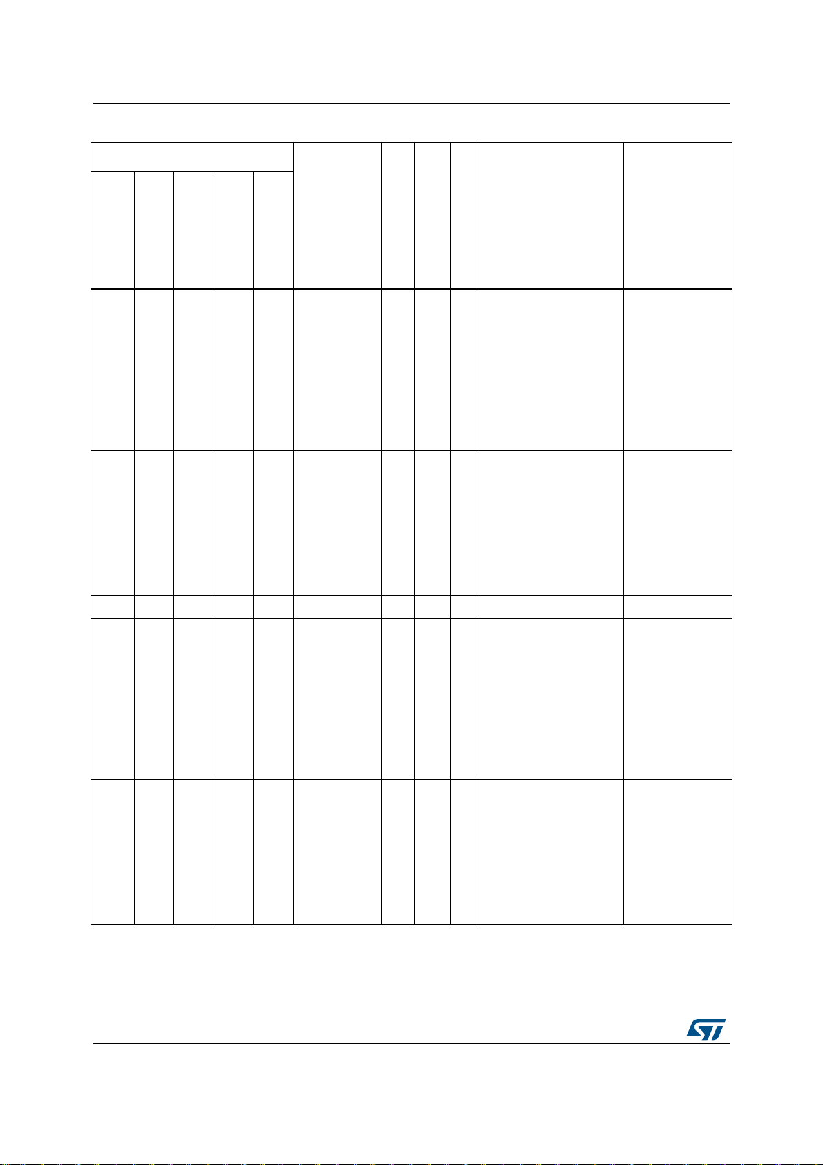
Pin descriptions STM32H747xI/G
Table 7. STM32H747xI/G pin/ball definition (continued)
Pin/ball name
Pin name
(function
after reset)
LQFP176
WLCSP156
D1 F10 124 144 E13 PC8 I/O
D2 E11 125 145 E14 PC9 I/O
- - 126 - L5 VDD S - - - -
UFBGA169
LQFP208
TFBGA240+25
Pin type
I/O structure
FT_
h
FT_f
h
Alternate functions
Notes
TRACED1,
HRTIM_CHB1,
TIM3_CH3, TIM8_CH3,
USART6_CK,
-
-
UART5_RTS/
UART5_DE,
FMC_NE2/FMC_NCE,
SWPMI_RX,
SDMMC1_D0,
DCMI_D2, EVENTOUT
MCO2, TIM3_CH4,
TIM8_CH4, I2C3_SDA,
I2S_CKIN, UART5_CTS,
QUADSPI_BK1_IO0,
LCD_G3,
SWPMI_SUSPEND,
SDMMC1_D1,
DCMI_D3, LCD_B2,
EVENTOUT
Additional
functions
-
-
D3 D10 127 146 E15 PA8 I/O
D4 D11 128 147 D15 PA9 I/O
FT_f
ha
FT_
u
MCO1, TIM1_CH1,
HRTIM_CHB2,
TIM8_BKIN2,
I2C3_SCL,
-
-
USART1_CK,
OTG_FS_SOF,
UART7_RX,
TIM8_BKIN2_COMP12,
LCD_B3, LCD_R6,
EVENTOUT
TIM1_CH2,
HRTIM_CHC1,
LPUART1_TX,
I2C3_SMBA,
SPI2_SCK/I2S2_CK,
USART1_TX,
FDCAN1_RXFD_MODE,
DCMI_D0, LCD_R5,
EVENTOUT
-
OTG_FS_VBUS
70/242 DS12930 Rev 1
Page 81

STM32H747xI/G Pin descriptions
Table 7. STM32H747xI/G pin/ball definition (continued)
Pin/ball name
WLCSP156
UFBGA169
Pin name
(function
after reset)
LQFP176
LQFP208
Pin type
I/O structure
Alternate functions
Notes
TFBGA240+25
Additional
functions
TIM1_CH3,
HRTIM_CHC2,
LPUART1_RX,
USART1_RX,
FDCAN1_TXFD_MODE,
OTG_FS_ID,
C2 A13 129 148 D14 PA10 I/O
FT_
u
-
MDIOS_MDIO, LCD_B4,
DCMI_D1, LCD_B1,
EVENTOUT
TIM1_CH4,
HRTIM_CHD1,
LPUART1_CTS,
SPI2_NSS/I2S2_WS,
-
UART4_RX,
USART1_CTS/USART1
C1 D12 130 149 E17 PA11 I/O
FT_
u
_NSS, FDCAN1_RX,
OTG_FS_DM, LCD_R4,
EVENTOUT
TIM1_ETR,
HRTIM_CHD2,
LPUART1_RTS/
LPUART1_DE,
SPI2_SCK/I2S2_CK,
B1 D13 131 150 E16 PA12 I/O
FT_
u
-
UART4_TX,
USART1_RTS/
USART1_DE,
SAI2_FS_B,
FDCAN1_TX,
OTG_FS_DP, LCD_R5,
EVENTOUT
C3 B11 132 151 C15
PA13(J TMS/
SWDIO)
I/O FT -
JTMS-SWDIO,
EVENTOUT
B2 C13 133 152 D17 VCAP S - - - -
A1 - 134 153 - VSS S - - - -
-
-
-
-
A2 B13 135 154 C17 VDDLDO - - - -
B3 - 136 155 K5 VDD S - - - -
TIM8_CH1N,
UART4_TX,
FDCAN1_TX,
FMC_D21, LCD_G2,
- - - 156 D16 PH13 I/O
FT_
h
-
EVENTOUT
DS12930 Rev 1 71/242
-
95
Page 82

Pin descriptions STM32H747xI/G
Table 7. STM32H747xI/G pin/ball definition (continued)
Pin/ball name
Pin name
(function
after reset)
LQFP176
WLCSP156
---157B17PH14I/O
---158B16PH15I/O
---159A16 PI0 I/O
---160- VSS S - - -
- B12 - 161 VDD VDD S - - -
---162A15 PI1 I/O
---163B15 PI2 I/O
---164C14 PI3 I/O
UFBGA169
LQFP208
TFBGA240+25
Pin type
I/O structure
FT_
h
FT_
h
FT_
h
FT_
h
FT_
h
FT_
h
Alternate functions
Notes
TIM8_CH2N,
UART4_RX,
-
-
-
-
-
-
FDCAN1_RX,
FMC_D22, DCMI_D4,
LCD_G3, EVENTOUT
TIM8_CH3N,
FDCAN1_TXFD_MODE,
FMC_D23, DCMI_D11,
LCD_G4, EVENTOUT
TIM5_CH4,
SPI2_NSS/I2S2_WS,
FDCAN1_RXFD_MODE,
FMC_D24, DCMI_D13,
LCD_G5, EVENTOUT
TIM8_BKIN2,
SPI2_SCK/I2S2_CK,
TIM8_BKIN2_COMP12,
FMC_D25, DCMI_D8,
LCD_G6, EVENTOUT
TIM8_CH4,
SPI2_MISO/I2S2_SDI,
FMC_D26, DCMI_D9,
LCD_G7, EVENTOUT
TIM8_ETR,
SPI2_MOSI/I2S2_SDO,
FMC_D27, DCMI_D10,
EVENTOUT
Additional
functions
-
-
-
-
-
-
C4 - 137 - - VSS S - - - -
B3 - - - VDD VDD S - - - -
E5 A11 138 165 B14
72/242 DS12930 Rev 1
PA14(JTCK/
SWCLK)
I/O FT -
JTCK-SWCLK,
EVENTOUT
-
Page 83
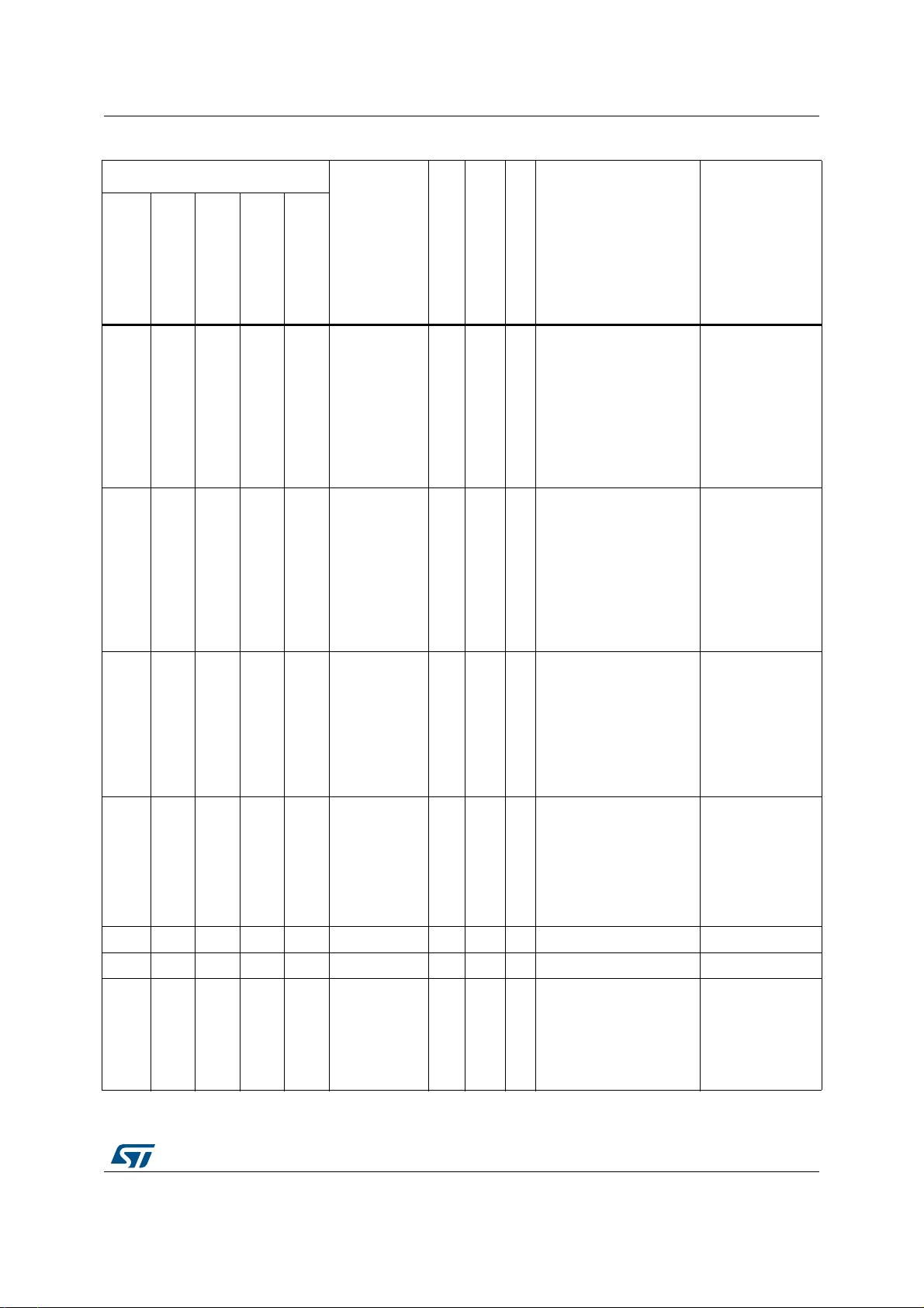
STM32H747xI/G Pin descriptions
Table 7. STM32H747xI/G pin/ball definition (continued)
Pin/ball name
Pin name
(function
WLCSP156
UFBGA169
after reset)
LQFP176
LQFP208
TFBGA240+25
Pin type
I/O structure
A3 B10 139 166 A14 PA15(JTDI) I/O FT -
D5 C11 140 167 A13 PC10 I/O
C5 E9 141 168 B13 PC11 I/O
FT_
ha
FT_
h
Alternate functions
Notes
JTDI,
TIM2_CH1/TIM2_ETR,
HRTIM_FLT1, CEC,
SPI1_NSS/I2S1_WS,
SPI3_NSS/I2S3_WS,
SPI6_NSS,
UART4_RTS/UART4_D
E, UART7_TX, DSI_TE,
EVENTOUT
HRTIM_EEV1,
DFSDM1_CKIN5,
SPI3_SCK/I2S3_CK,
USART3_TX,
-
UART4_TX,
QUADSPI_BK1_IO1,
SDMMC1_D2,
DCMI_D8, LCD_R2,
EVENTOUT
HRTIM_FLT2,
DFSDM1_DATIN5,
SPI3_MISO/I2S3_SDI,
-
USART3_RX,
UART4_RX,
QUADSPI_BK2_NCS,
SDMMC1_D3,
DCMI_D4, EVENTOUT
Additional
functions
-
-
-
TRACED3,
HRTIM_EEV2,
SPI3_MOSI/I2S3_SDO,
-
USART3_CK,
UART5_TX,
-
B4 D9 142 169 C12 PC12 I/O
FT_
h
SDMMC1_CK,
DCMI_D9, EVENTOUT
-A7--- VSS S-- - -
- ---VDD VDD S-- - -
DFSDM1_CKIN6,
SAI3_SCK_A,
A4 C10 143 170 D13 PD0 I/O
FT_
h
-
UART4_RX,
FDCAN1_RX,
-
FMC_D2/FMC_DA2,
EVENTOUT
DS12930 Rev 1 73/242
95
Page 84

Pin descriptions STM32H747xI/G
Table 7. STM32H747xI/G pin/ball definition (continued)
Pin/ball name
Pin name
(function
after reset)
LQFP176
WLCSP156
F6 C9 144 171 E12 PD1 I/O
E6 E8 145 172 D12 PD2 I/O
B5 A10 146 173 B12 PD3 I/O
A5 D8 147 174 A12 PD4 I/O
F7 C8 148 175 A11 PD5 I/O
UFBGA169
LQFP208
TFBGA240+25
Pin type
I/O structure
FT_
h
FT_
h
FT_
h
FT_
h
FT_
h
Alternate functions
Notes
DFSDM1_DATIN6,
SAI3_SD_A,
-
-
-
-
-
UART4_TX,
FDCAN1_TX,
FMC_D3/FMC_DA3,
EVENTOUT
TRACED2, TIM3_ETR,
UART5_RX,
SDMMC1_CMD,
DCMI_D11, EVENTOUT
DFSDM1_CKOUT,
SPI2_SCK/I2S2_CK,
USART2_CTS/USART2
_NSS, FMC_CLK,
DCMI_D5, LCD_G7,
EVENTOUT
HRTIM_FLT3,
SAI3_FS_A,
USART2_RTS/USART2
_DE,
FDCAN1_RXFD_MODE,
FMC_NOE, EVENTOUT
HRTIM_EEV3,
USART2_TX,
FDCAN1_TXFD_MODE,
FMC_NWE, EVENTOUT
Additional
functions
-
-
-
-
-
B6---- VSS S-- - -
A6 B2 - - VDD VDD S - - - -
SAI1_D1,
DFSDM1_CKIN4,
DFSDM1_DATIN1,
SPI3_MOSI/I2S3_SDO,
SAI1_SD_A,
C6 B8 149 176 B11 PD6 I/O
74/242 DS12930 Rev 1
FT_
h
-
USART2_RX,
SAI4_SD_A,
FDCAN2_RXFD_MODE,
SAI4_D1, SDMMC2_CK,
FMC_NWAIT,
DCMI_D10, LCD_B2,
EVENTOUT
-
Page 85

STM32H747xI/G Pin descriptions
Table 7. STM32H747xI/G pin/ball definition (continued)
Pin/ball name
WLCSP156
UFBGA169
Pin name
(function
after reset)
LQFP176
LQFP208
Pin type
I/O structure
Alternate functions
Notes
TFBGA240+25
Additional
functions
DFSDM1_DATIN4,
SPI1_MOSI/I2S1_SDO,
DFSDM1_CKIN1,
SPDIFRX1_IN0,
USART2_CK,
D6 A8 150 177 C11 PD7 I/O
FT_
h
SDMMC2_CMD,
FMC_NE1, EVENTOUT
- ---D11 PJ12 I/OFT-
- ---E10 PJ13 I/OFT-
TRGOUT, LCD_G3,
LCD_B0, EVENTOUT
LCD_B4, LCD_B1,
EVENTOUT
- - - - D10 PJ14 I/O FT - LCD_B2, EVENTOUT -
- - - - B10 PJ15 I/O FT - LCD_B3, EVENTOUT -
B9 B9 151 178 - VSS S - - - -
- - 152 179 VDD VDD S - - - -
SPI1_MISO/I2S1_SDI,
USART6_RX,
SPDIFRX1_IN4,
- C7 153 180 A10 PG9 I/O
FT_
h
QUADSPI_BK2_IO2,
-
SAI2_FS_B,
FMC_NE2/FMC_NCE,
DCMI_VSYNC,
EVENTOUT
-
-
-
-
- D7 154 181 A9 PG10 I/O
- E7 155 182 B9 PG11 I/O
DS12930 Rev 1 75/242
FT_
h
FT_
h
HRTIM_FLT5,
SPI1_NSS/I2S1_WS,
-
LCD_G3, SAI2_SD_B,
FMC_NE3, DCMI_D2,
LCD_B2, EVENTOUT
LPTIM1_IN2,
HRTIM_EEV4,
SPI1_SCK/I2S1_CK,
-
SPDIFRX1_IN1,
SDMMC2_D2,
ETH_MII_TX_EN/ETH_
RMII_TX_EN, DCMI_D3,
LCD_B3, EVENTOUT
-
-
95
Page 86

Pin descriptions STM32H747xI/G
Table 7. STM32H747xI/G pin/ball definition (continued)
Pin/ball name
Pin name
(function
after reset)
LQFP176
WLCSP156
- G7 156 183 C9 PG12 I/O
- F7 157 184 D9 PG13 I/O
- E6 158 185 D8 PG14 I/O
UFBGA169
LQFP208
TFBGA240+25
Pin type
I/O structure
FT_
h
FT_
h
FT_
h
Alternate functions
Notes
LPTIM1_IN1,
HRTIM_EEV5,
SPI6_MISO,
USART6_RTS/USART6
-
_DE, SPDIFRX1_IN2,
LCD_B4,
ETH_MII_TXD1/ETH_R
MII_TXD1, FMC_NE4,
LCD_B1, EVENTOUT
TRACED0,
LPTIM1_OUT,
HRTIM_EEV10,
SPI6_SCK,
-
USART6_CTS/USART6
_NSS,
ETH_MII_TXD0/ETH_R
MII_TXD0, FMC_A24,
LCD_R0, EVENTOUT
TRACED1,
LPTIM1_ETR,
SPI6_MOSI,
-
USART6_TX,
QUADSPI_BK2_IO3,
ETH_MII_TXD1/ETH_R
MII_TXD1, FMC_A25,
LCD_B0, EVENTOUT
Additional
functions
-
-
-
- - 159 186 - VSS S - - - -
- - 160 187 VDD VDD S - - - -
- - - - C8 PK3 I/O FT - LCD_B4, EVENTOUT -
- - - - B8 PK4 I/O FT - LCD_B5, EVENTOUT -
- - - - A8 PK5 I/O FT - LCD_B6, EVENTOUT -
- - - - C7 PK6 I/O FT - LCD_B7, EVENTOUT -
- - - - D7 PK7 I/O FT - LCD_DE, EVENTOUT -
-B7- -VDD VDD S - - -
A7 C6 161 188 D6 PG15 I/O
76/242 DS12930 Rev 1
FT_
h
USART6_CTS/USART6
-
_NSS, FMC_SDNCAS,
DCMI_D13, EVENTOUT
-
Page 87

STM32H747xI/G Pin descriptions
Table 7. STM32H747xI/G pin/ball definition (continued)
Pin/ball name
Pin name
(function
LQFP176
WLCSP156
UFBGA169
LQFP208
B7 A6 162 189 C6
after reset)
TFBGA240+25
PB3(JTDO/TR
ACESWO)
Pin type
I/O structure
I/O FT -
A8 B6 163 190 B7 PB4(NJTRST) I/O FT -
B8 A5 164 191 A5 PB5 I/O FT -
Alternate functions
Notes
JTDO/TRACESWO,
TIM2_CH2,
HRTIM_FLT4,
SPI1_SCK/I2S1_CK,
SPI3_SCK/I2S3_CK,
SPI6_SCK,
SDMMC2_D2,
CRS_SYNC,
UART7_RX,
EVENTOUT
NJTRST, TIM16_BKIN,
TIM3_CH1,
HRTIM_EEV6,
SPI1_MISO/I2S1_SDI,
SPI3_MISO/I2S3_SDI,
SPI2_NSS/I2S2_WS,
SPI6_MISO,
SDMMC2_D3,
UART7_TX, EVENTOUT
TIM17_BKIN,
TIM3_CH2,
HRTIM_EEV7,
I2C1_SMBA,
SPI1_MOSI/I2S1_SDO,
I2C4_SMBA,
SPI3_MOSI/I2S3_SDO,
SPI6_MOSI,
FDCAN2_RX,
OTG_HS_ULPI_D7,
ETH_PPS_OUT,
FMC_SDCKE1,
DCMI_D10, UART5_RX,
EVENTOUT
Additional
functions
-
-
-
A9 - - - VDD VDD S - - - -
DS12930 Rev 1 77/242
95
Page 88

Pin descriptions STM32H747xI/G
Table 7. STM32H747xI/G pin/ball definition (continued)
Pin/ball name
Pin name
(function
after reset)
LQFP176
WLCSP156
C7 E5 165 192 B5 PB6 I/O FT_f -
C8 C5 166 193 C5 PB7 I/O
UFBGA169
LQFP208
TFBGA240+25
Pin type
I/O structure
FT_f
a
Alternate functions
Notes
TIM16_CH1N,
TIM4_CH1,
HRTIM_EEV8,
I2C1_SCL, CEC,
I2C4_SCL,
USART1_TX,
LPUART1_TX,
FDCAN2_TX,
QUADSPI_BK1_NCS,
DFSDM1_DATIN5,
FMC_SDNE1,
DCMI_D5, UART5_TX,
EVENTOUT
TIM17_CH1N,
TIM4_CH2,
HRTIM_EEV9,
I2C1_SDA, I2C4_SDA,
USART1_RX,
-
LPUART1_RX,
FDCAN2_TXFD_MODE,
DFSDM1_CKIN5,
FMC_NL,
DCMI_VSYNC,
EVENTOUT
Additional
functions
-
PVD_IN
D7 B5 167 194 E8 BOOT0 I B - - VPP
TIM16_CH1, TIM4_CH3,
DFSDM1_CKIN7,
I2C1_SCL, I2C4_SCL,
SDMMC1_CKIN,
A10 D5 168 195 D5 PB8 I/O
78/242 DS12930 Rev 1
FT_f
h
-
UART4_RX,
FDCAN1_RX,
SDMMC2_D4,
ETH_MII_TXD3,
SDMMC1_D4,
DCMI_D6, LCD_B6,
EVENTOUT
-
Page 89
STM32H747xI/G Pin descriptions
Table 7. STM32H747xI/G pin/ball definition (continued)
Pin/ball name
WLCSP156
UFBGA169
Pin name
(function
after reset)
LQFP176
LQFP208
Pin type
I/O structure
Alternate functions
Notes
TFBGA240+25
Additional
functions
TIM17_CH1, TIM4_CH4,
DFSDM1_DATIN7,
I2C1_SDA,
SPI2_NSS/I2S2_WS,
I2C4_SDA,
SDMMC1_CDIR,
UART4_TX,
FDCAN1_TX,
C9 D6 169 196 D4 PB9 I/O
FT_f
h
-
SDMMC2_D5,
I2C4_SMBA,
SDMMC1_D5,
DCMI_D7, LCD_B7,
EVENTOUT
LPTIM1_ETR,
TIM4_ETR,
HRTIM_SCIN,
LPTIM2_ETR,
UART8_RX,
FDCAN1_RXFD_MODE,
B10 D4 170 197 C4 PE0 I/O
FT_
h
-
SAI2_MCLK_A,
FMC_NBL0, DCMI_D2,
EVENTOUT
LPTIM1_IN2,
HRTIM_SCOUT,
D8 C4 171 198 B4 PE1 I/O
FT_
h
-
UART8_TX,
FDCAN1_TXFD_MODE,
FMC_NBL1, DCMI_D3,
EVENTOUT
A11 A4 172 199 A7 VCAP S - - - -
-
-
-
C10 - 173 200 B6 VSS S - - - -
E7 B3 174 201 E7 PDR_ON I FT - - -
A12 A3 175 202 A6 VDDLDO S - - - -
B11 - - - VDD VDD S - - - -
TIM8_BKIN,
SAI2_MCLK_A,
TIM8_BKIN_COMP12,
FMC_NBL2, DCMI_D5,
- - - 203 A4 PI4 I/O
FT_
h
-
LCD_B4, EVENTOUT
DS12930 Rev 1 79/242
-
95
Page 90

Pin descriptions STM32H747xI/G
Table 7. STM32H747xI/G pin/ball definition (continued)
Pin/ball name
WLCSP156
UFBGA169
Pin name
(function
after reset)
LQFP176
LQFP208
Pin type
I/O structure
Alternate functions
Notes
TFBGA240+25
Additional
functions
TIM8_CH1,
SAI2_SCK_A,
FMC_NBL3,
DCMI_VSYNC,
-
- - - 204 A3 PI5 I/O
FT_
h
-
LCD_B5, EVENTOUT
TIM8_CH2, SAI2_SD_A,
-
FMC_D28, DCMI_D6,
LCD_B6, EVENTOUT
TIM8_CH3, SAI2_FS_A,
-
FMC_D29, DCMI_D7,
LCD_B7, EVENTOUT
-
-
- - - 205 A2 PI6 I/O
- - - 206 B3 PI7 I/O
FT_
h
FT_
h
---207- VSS S-- - -
B11 - 176 208 VDD VDD S - - - -
M13---- VSS S-- - -
A13---- DNC -- - -
- - - - M15 VSSDSI S - - - -
1. When this pin/ball was previously configured as an oscillator, the oscillator function is kept during and after a reset. This is
valid for all resets except for power-on reset.
2. Pxy_C and Pxy pins/balls are two separate pads (analog switch open). The analog switch is configured through a SYSCFG
register. Refer to the product reference manual for a detailed description of the switch configuration bits.
3. There is a direct path between Pxy_C and Pxy pins/balls, through an analog switch. Pxy alternate functions are available on
Pxy_C when the analog switch is closed. The analog switch is configured through a SYSCFG register. Refer to the product
reference manual for a detailed description of the switch configuration bits.
80/242 DS12930 Rev 1
Page 91

DS12930 Rev 1 81/242
AF0 AF1 AF2 AF3 AF4 AF5 AF6 AF7 AF8 AF9 AF10 AF11 AF12 AF13 AF14 AF15
Port
PA0 -
PA1 - TIM2_CH2 TIM5_CH2
PA2 TIM2_CH3 TIM5_CH3
PA3 TIM2_CH4 TIM5_CH4
D1PWR
PA4
D2PWRETIM2_CH1/
PA5
PA6 - TIM1_BKIN TIM3_CH1 TIM8_BKIN -
Port A
PA7 - TIM1_CH1N TIM3_CH2 TIM8_CH1N -
PA8 M CO1 T IM 1_C H1
PA9 - TI M1 _CH 2
PA1 0 - T IM1 _C H3
PA11 - TI M1 _CH 4
PA1 2 - T IM1 _E TR
SYS
E
TIM1/2/16/1
7/LPTIM1/
HRTIM1
TIM2_CH1/
TIM2_ETR
TIM2_ETR
SAI1/TIM3/
4/5/HRTIM
TIM5_CH1 TIM8_ETR TIM15_BKIN - -
-TIM5_ETR- -
HRTIM_
CHB2
HRTIM_
CHC1
HRTIM_
CHC2
HRTIM_
CHD1
HRTIM_
CHD2
LPUART/
TIM8/LPTIM
1
2/3/4/5/
HRTIM1/
DFSDM1
LPTIM3_
OUT
LPTIM4_
OUT
LPTIM5_
OUT
-TIM8_CH1N -
TIM8_BKIN2 I2C3_SCL - -
LPUART1_
TX
LPUART1_
RX
LPUART1_
CTS
LPUART1_
RTS/
LPUART1_
DE
Table 8. Port A alternate functions
I2C1/2/3/4/U
SART1/
TIM15/
LPTIM2/
DFSDM1/CE
TIM15_
CH1N
TIM15_CH1 - -
TIM15_CH2 - -
I2C3_SMBA
SPI1/2/3/4/
5/6/CEC
C
SPI1_NSS/
I2S1_WS
SPI1_SCK/
I2S1_CK
SPI1_MISO
/I2S1_SDI
SPI1_MOSI
/I2S1_SDO
SPI2_SCK/
I2S2_CK
---
SPI2_NSS/
I2S2_WS
SPI2_SCK/
-
I2S2_CK
SPI2/3/SAI1
/3/I2C4/
UART4/
DFSDM1
--
SPI3_NSS/
I2S3_WS
--SPI6_SCK-
- - SPI6_MISO
- - SPI6_MOSI
-
UART4_RX
UART4_TX
SPI2/3/6/
USART1/2/
3/6/UART7/
SDMMC1
USART2_
CTS/USAR
T2_NSS
USART2_
RTS/
USART2_
USART2_TXSAI2_SCK
USART2_
USART2_C
USART1_
USART1_
USART1_
USART1_
CTS/
USART1_
NSS
USART1_
RTS/
USART1_
SPI6/SAI2/
4/UART4/5/
8/LPUART/
SDMMC1/
SPDIFRX1
UART4_TX
UART4_RX
DE
_B
RX
K
CK
TX
RX
DE
-LCD_B2
SPI6_NSS - - -
--
-
-
-
SAI2_FS_B
SAI4/FDCA
N1/FDACN
2/TIM13/14
/QUADSPI/
FMC/SDM
MC2/LCD/
SPDIFRX1
SDMMC2_
CMD
QUADSPI_
BK1_IO3
TIM13_CH1TIM8_BKIN
TIM14_
FDCAN1_
RXFD_
MODE
FDCAN1_
TXFD_
MODE
FDCAN1_RXOTG_FS_
FDCAN1_TXOTG_FS_
SAI2/4/TIM
8/QUADSPI
/SDMMC2/
OTG1_HS/
OTG2_FS/
SAI2_SD_B
SAI2_MCLK
--ETH_MDIO
OTG_HS_
ULPI_D0
OTG_HS_
ULPI_CK
_COMP12
CH1
OTG_FS_
OTG_FS_IDMDIOS_
LCD
_B
SOF
DM
DP
-
I2C4/UART
7/SWPMI1/
TIM1/8/
DFSDM1/
SDMMC2/
MDIOS/
ETH
ETH_MII_
CRS
ETH_MII_
RX_CLK/
ETH_RMII_
REF_CLK
ETH_MII_
COL
--- LCD_R4
MDIOS_
MDC
ETH_MII_R
X_DV/ETH_
RMII_CRS_
DV
UART7_RX
ETH_TX_
ER
MDIO
--- LCD_R4
--- LCD_R5
TIM1/8/FMC
/SDMMC1/
MDIOS/
OTG1_FS/
MDIOS_
MDIO
OTG_HS_
TIM1_BKIN
_COMP12
FMC_
SDNWE
TIM8_BKIN
2_COMP12
LCD_B4 DCMI_D1 LCD_B1
TIM1/DCMI/
LCD/DSI/
LCD
- - -
- - LCD_R2
- - LCD_B5
SOF
- DCMI_D0 LCD_R5
COMP
DCMI_HSYNCLCD_VSYNCEVENT
DCMI_PIXC
LK
LCD_B3 LCD_R6
UART5/
- LCD_R1
LCD_G2
- -
LCD
SYS
EVENT
OUT
EVENT
OUT
EVENT
OUT
EVENT
OUT
OUT
EVENT
OUT
EVENT
OUT
EVENT
OUT
EVENT
OUT
EVENT
OUT
EVENT
OUT
EVENT
OUT
EVENT
OUT
STM32H747xI/G Pin descriptions
Page 92

82/242 DS12930 Rev 1
Port
PA1 3
PA1 4
Port A
PA1 5 J TDI
Table 8. Port A alternate functions (continued)
AF0 AF1 AF2 AF3 AF4 AF5 AF6 AF7 AF8 AF9 AF10 AF11 AF12 AF13 AF14 AF15
SYS
JTMS/
SWDIO
JTCK/
SWCLK
4_DE
SAI4/FDCA
N1/FDACN
2/TIM13/14
/QUADSPI/
FMC/SDM
MC2/LCD/
SPDIFRX1
SAI2/4/TIM
8/QUADSPI
/SDMMC2/
OTG1_HS/
OTG2_FS/
--UART7_TX-DSI_TE -
I2C1/2/3/4/U
SART1/
TIM15/
LPTIM2/
DFSDM1/CE
-CEC
SPI1/2/3/4/
5/6/CEC
C
SPI1_NSS/
I2S1_WS
SPI2/3/SAI1
/3/I2C4/
UART4/
DFSDM1
SPI3_NSS/
I2S3_WS
SPI2/3/6/
USART1/2/
3/6/UART7/
SDMMC1
SPI6_NSS
SPI6/SAI2/
4/UART4/5/
8/LPUART/
SDMMC1/
SPDIFRX1
UART4_
RTS/UART
1
LPUART/
TIM8/LPTIM
2/3/4/5/
HRTIM1/
DFSDM1
TIM1/2/16/1
7/LPTIM1/
HRTIM1
TIM2_CH1/
TIM2_ETR
SAI1/TIM3/
4/5/HRTIM
- - - - - - ---- - - - -
- - - - - - ---- - - - -
HRTIM_FL
T1
LCD
I2C4/UART
7/SWPMI1/
TIM1/8/
DFSDM1/
SDMMC2/
MDIOS/
ETH
TIM1/8/FMC
/SDMMC1/
MDIOS/
OTG1_FS/
LCD
TIM1/DCMI/
LCD/DSI/
COMP
UART5/
LCD
SYS
EVENT
OUT
EVENT
OUT
EVENT
OUT
Pin descriptions STM32H747xI/G
Page 93

AF0 AF1 AF2 AF3 AF4 AF5 AF6 AF7 AF8 AF9 AF10 AF11 AF12 AF13 AF14 AF15
I2C1/2/3/4/U
SART1/
TIM15/
LPTIM2/
DFSDM1/
CEC
DFSDM1_
CKIN1
--
1
LPUART/
TIM8/LPTIM
2/3/4/5/
HRTIM1/
DFSDM1
Port
PB0 - TIM1_CH2N TIM3_CH3 TIM8_CH2N - -
PB1 - TIM1_CH3N TIM3_CH4 TIM8_CH3N - -
PB2
PB3
TRACESWOTIM2_CH2
SYS
RTC_
OUT
JTDO/
TIM1/2/16/1
7/LPTIM1/
HRTIM1
SAI1/TIM3/
4/5/HRTIM
- SAI1_D1 -
HRTIM_
FLT4
Table 9. Port B alternate functions
SPI6/SAI2/
4/UART4/5/
8/LPUART/
SDMMC1/
SPDIFRX1
UART4_
-
- - LCD_R6
- SPI6_SCK
CTS
SAI4_SD_AQUADSPI_
SPI1/2/3/4/
5/6/CEC
- SAI1_SD_A
SPI1_SCK/
I2S1_CK
SPI2/3/SAI1
/3/I2C4/
UART4/
DFSDM1
DFSDM1_C
KOUT
DFSDM1_
DATIN1
SPI3_SCK/I
2S3_CK
SPI2/3/6/
USART1/2/
3/6/UART7/
SDMMC1
SPI3_MOSI
/I2S3_SDO
SAI4/FDCA
N1/FDACN
2/TIM13/14
/QUADSPI/
FMC/SDM
MC2/LCD/
SPDIFRX1
LCD_R3
CLK
SDMMC2_
D2
SAI2/4/TIM
8/QUADSPI
/SDMMC2/
OTG1_HS/
OTG2_FS/
LCD/CRS
OTG_HS_
ULPI_D1
OTG_HS_
ULPI_D2
SAI4_D1 - - - -
CRS_SYNC UART7_RX - - -
I2C4/UART
7/SWPMI1/
TIM1/8/
DFSDM1/
SDMMC2/
MDIOS/
ETH
ETH_MII_
RXD2
ETH_MII_
RXD3
TIM1/8/FMC
/SDMMC1/
MDIOS/
OTG1_FS/
TIM1/DCMI/
LCD/DSI/
LCD
- - LCD_G1
--LCD_G0
COMP
UART5/
LCD
SYS
EVENT
OUT
EVENT
OUT
EVENT
OUT
EVENT
OUT
STM32H747xI/G Pin descriptions
DS12930 Rev 1 83/242
PB4 NJTRST TIM16_BKIN TIM3_CH1
Port B
PB5 - TIM17_BKIN TIM3_CH2
PB6 -
PB7 -
PB8 - TIM16_CH1 TIM4_CH3
TIM16_CH1
N
TIM17_CH1
N
TIM4_CH1
TIM4_CH2
HRTIM_EEV
6
HRTIM_EEV
7
HRTIM_EEV
8
HRTIM_EEV
9
DFSDM1_C
KIN7
SPI1_MISO
/I2S1_SDI
I2C1_SMBA
I2C1_SCL CEC I2C4_SCL
I2C1_SDA - I2C4_SDA
I2C1_SCL - I2C4_SCL
SPI1_MOSI
/I2S1_SDO
SPI3_MISO/
I2S3_SDI
I2C4_SMBA
SPI2_NSS/
I2S2_WS
SPI3_MOSI
/I2S3_SDO
USART1_TXLPUART1_TXFDCAN2_TXQUADSPI_
USART1_RXLPUART1_
SDMMC1_
CKIN
SPI6_MISO
SPI6_MOSI
UART4_RX
SDMMC2_
D3
FDCAN2_RXOTG_HS_U
BK1_NCS
FDCAN2_
RX
TXFD_
MODE
FDCAN1_RXSDMMC2_D4ETH_MII_
-UART7_TX - - -
LPI_D7
-
ETH_PPS_
OUT
DFSDM1_D
ATI N5
DFSDM1_C
KIN5
TXD3
FMC_SDCK
E1
FMC_SDNE
1
FMC_NL
SDMMC1_
D4
DCMI_D10
DCMI_D5
DCMI_VSY
DCMI_D6 LCD_B6
UART5_RXEVENT
UART5_TXEVENT
NC
EVENT
OUT
OUT
OUT
EVENT
OUT
EVENT
OUT
Page 94

84/242 DS12930 Rev 1
AF0 AF1 AF2 AF3 AF4 AF5 AF6 AF7 AF8 AF9 AF10 AF11 AF12 AF13 AF14 AF15
Port
PB9 - TIM17_CH1 TIM4_CH4
PB10 - TIM2_CH3
PB11 - TIM2_CH4
PB12 - TIM1_BKIN - - I2C2_SMBA
Port B
PB13 - TIM1_CH1N -
PB14 - TIM1_CH2N - TIM8_CH2N USART1_TX
RTC_RE
PB15
TIM1/2/16/1
SYS
7/LPTIM1/
HRTIM1
TIM1_CH3N - TIM8_CH3N USART1_RX
FIN
SAI1/TIM3/
4/5/HRTIM
HRTIM_SC
OUT
HRTIM_
SCIN
LPUART/
TIM8/LPTIM
1
2/3/4/5/
HRTIM1/
DFSDM1
DFSDM1_
DATIN7
LPTIM2_IN1 I2C2_SCL
LPTIM2_
ETR
LPTIM2_
OUT
I2C1/2/3/4/U
SART1/
TIM15/
LPTIM2/
DFSDM1/
CEC
I2C1_SDA
I2C2_SDA -
Table 9. Port B alternate functions (continued)
SAI4/FDCA
N1/FDACN
2/TIM13/14
/QUADSPI/
FMC/SDM
MC2/LCD/
SPDIFRX1
FDCAN1_TXSDMMC2_
QUADSPI_
BK1_NCS
--
FDCAN2_RXOTG_HS_U
-
FDCAN2_TXOTG_HS_
-
SDMMC2_
RTS/
CTS
D0
SDMMC2_
D1
TX
RX
CK
SS
DE
-
SPI6/SAI2/
4/UART4/5/
8/LPUART/
SDMMC1/
SPDIFRX1
UART4_TX
UART4_
UART4_DE
UART4_
SPI1/2/3/4/
5/6/CEC
SPI2_NSS/
I2S2_WS
SPI2_SCK/
I2S2_CK
SPI2_NSS/
I2S2_WS
SPI2_SCK/
I2S2_CK
SPI2_MISO
/I2S2_SDI
SPI2_MOSI
/I2S2_SDO
SPI2/3/SAI1
/3/I2C4/
UART4/
DFSDM1
I2C4_SDA
DFSDM1_
DATIN7
DFSDM1_
CKIN7
DFSDM1_
DATIN1
DFSDM1_
CKIN1
DFSDM1_
DATIN2
DFSDM1_
CKIN2
SPI2/3/6/
USART1/2/
3/6/UART7/
SDMMC1
SDMMC1_
CDIR
USART3_
USART3_
USART3_
USART3_
CTS/
USART3_N
USART3_
RTS/
USART3_
SAI2/4/TIM
8/QUADSPI
/SDMMC2/
OTG1_HS/
OTG2_FS/
LCD/CRS
OTG_HS_
ULPI_D3
OTG_HS_
ULPI_D4
LPI_D5
ULPI_D6
I2C4/UART
7/SWPMI1/
TIM1/8/
DFSDM1/
SDMMC2/
MDIOS/
ETH
I2C4_SMBA
D5
ETH_MII_
RX_ER
ETH_MII_
TX_EN/ETH
_RMII_TX_
EN
ETH_MII_
TXD0/ETH_
RMII_TXD0
ETH_MII_
TXD1/ETH_
RMII_TXD1
--
--
TIM1/8/FMC
/SDMMC1/
MDIOS/
OTG1_FS/
SDMMC1_
OTG_HS_IDTIM1_BKIN
OTG_HS_
OTG_HS_
TIM1/DCMI/
LCD/DSI/
LCD
D5
--LCD_G4
- DSI_TE LCD_G5
--
DM
DP
COMP
DCMI_D7 LCD_B7
_COMP12
-
-
UART5/
LCD
UART5_RXEVENT
UART5_TXEVENT
SYS
EVENT
OUT
EVENT
OUT
EVENT
OUT
OUT
OUT
EVENT
OUT
EVENT
OUT
Pin descriptions STM32H747xI/G
Page 95

DS12930 Rev 1 85/242
AF0 AF1 AF2 AF3 AF4 AF5 AF6 AF7 AF8 AF9 AF10 AF11 AF12 AF13 AF14 AF15
Port
PC0 - - -
TRACED
PC1
PC2
DSLEEP
PC3
SLEEP
PC4
DSLEEP
PC5
SLEEP
PC6 -
PC7 TRGIO
Port C
TRACED1HRTIM_CH
PC8
PC9 MCO2 - TIM3_CH4 TIM8_CH4 I2C3_SDA I2S_CKIN - -
PC10 - -
PC11 - -
TRACED
PC12
PC13-- - - - - - --- - - - --
PC14-- - - - - - --- - - - --
PC15-- - - - - - --- - - - --
SYS
C1
C1
C2
C2
0
3
TIM1/2/16/1
7/LPTIM1/
HRTIM1
HRTIM_CH
HRTIM_CH
SAI1/TIM3/
4/5/HRTIM
-SAI1_D1
--
--
--
-SAI1_D3
TIM3_CH1 TIM8_CH1
A1
TIM3_CH2 TIM8_CH2
A2
TIM3_CH3 TIM8_CH3 - - -
B1
HRTIM_EEV1DFSDM1_
HRTIM_FLT2DFSDM1_
HRTIM_EE
V2
LPUART/
TIM8/LPTIM
1
2/3/4/5/
HRTIM1/
DFSDM1
DFSDM1_C
KIN0
DFSDM1_
DATIN0
DFSDM1_
CKIN1
DFSDM1_
DATIN1
DFSDM1_
CKIN2
DFSDM1_
DATIN2
CKIN5
DATIN5
I2C1/2/3/4/U
SART1/
TIM15/
LPTIM2/
DFSDM1/
CEC
DFSDM1_
CKIN4
DFSDM1_
CKIN3
DFSDM1_
DATIN3
---
Table 10. Port C alternate functions
RTS/
CTS
SAI4/FDCA
N1/FDACN
2/TIM13/14
/QUADSPI/
FMC/SDM
MC2/LCD/
SPDIFRX1
SPDIFRX1
SPDIFRX1
FMC_
NWAIT
FMC_NE1
FMC_NE2/
FMC_NCE
QUADSPI_
BK1_IO0
QUADSPI_
BK1_IO1
QUADSPI_
BK2_NCS
SPI1/2/3/4/
5/6/CEC
- -
SPI2_MOSI
/I2S2_SDO
SPI2_MISO
/I2S2_SDI
SPI2_MOSI
-
/I2S2_SDO
- I2S1_MCK - -
-----
I2S2_MCK -
--
--
SPI2/3/SAI1
/3/I2C4/
UART4/
DFSDM1
DFSDM1_
DATIN4
SAI1_SD_A -
DFSDM1_
CKOUT
-I2S3_MCK
SPI3_SCK/
I2S3_CK
SPI3_MISO/
I2S3_SDI
SPI3_MOSI/
I2S3_SDO
SPI2/3/6/
USART1/2/
3/6/UART7/
SDMMC1
- ---
USART6_TXSDMMC1_
USART6_RXSDMMC1_
USART6_
USART3_
USART3_
USART3_
SPI6/SAI2/
4/UART4/5/
8/LPUART/
SDMMC1/
SPDIFRX1
- SAI2_FS_B -
SAI4_SD_ASDMMC2_
---
D0DIR
D123DIR
UART5_
CK
UART5_DE
UART5_
UART4_TX
TX
UART4_RX
RX
UART5_TX - - -
CK
CK
_IN3
_IN4
SAI2/4/TIM
8/QUADSPI
/SDMMC2/
OTG1_HS/
OTG2_FS/
OTG_HS_
ULPI_STP
SAI4_D1 ETH_MDC
OTG_HS_
ULPI_DIR
OTG_HS_U
LPI_NXT
SAI4_D3
SDMMC2_
SDMMC2_
LCD_G3
I2C4/UART
7/SWPMI1/
TIM1/8/
DFSDM1/
SDMMC2/
LCD
-
D6
D7
-SWPMI_RX
--
--
MDIOS/
ETH
-
ETH_MII_
TXD2
ETH_MII_
TX_CLK
ETH_MII_
RXD0/ETH_
RMII_RXD0
ETH_MII_
RXD1/ETH_
RMII_RXD1
-
SWPMI_TX
SWPMI_
SUSPEND
TIM1/8/FMC
/SDMMC1/
MDIOS/
OTG1_FS/
LCD
FMC_SDN
WE
MDIOS_
MDC
FMC_SDNE
0
FMC_SDCK
E0
FMC_SDNE
0
FMC_
SDCKE0
SDMMC1_
D6
SDMMC1_
D7
SDMMC1_
D0
SDMMC1_
D1
SDMMC1_
D2
SDMMC1_
D3
SDMMC1_
CK
TIM1/DCMI/
LCD/DSI/
COMP
COMP1_
OUT
DCMI_D0
DCMI_D1 LCD_G6
DCMI_D2 -
DCMI_D3 LCD_B2
DCMI_D8 LCD_R2
DCMI_D4 -
DCMI_D9 -
UART5/
LCD
- LCD_R5
--
--
--
--
-
LCD_
HSYNC
SYS
EVENT
OUT
EVENT
OUT
EVENT
OUT
EVENT
OUT
EVENT
OUT
EVENT
OUT
EVENT
OUT
EVENT
OUT
EVENT
OUT
EVENT
OUT
EVENT
OUT
EVENT
OUT
EVENT
OUT
EVENT
OUT
EVENT
OUT
EVENT
OUT
STM32H747xI/G Pin descriptions
Page 96

86/242 DS12930 Rev 1
AF0 AF1 AF2 AF3 AF4 AF5 AF6 AF7 AF8 AF9 AF10 AF11 AF12 AF13 A F14 AF15
Port
PD0 - - -
PD1 - - -
PD2
PD3 - - -
PD4 - -
PD5 - -
PD6 - - SAI1_D1
Port D
PD7 - - -
PD8 - - -
PD9 - - -
PD10 - - -
PD11 - - -
PD12 -
PD13 -
SYS
TRACE
D2
TIM1/2/16/
17/LPTIM1
HRTIM1
LPTIM1_IN
LPTIM1_
SAI1/TIM3/
/
- TIM3_ETR - - - - - UART5_RX - - -
HRTIM_EE
1
OUT
Table 11. Port D alternate functions
LPUART/
4/5/HRTIM
HRTIM_
FLT3
TIM4_CH1
TIM4_CH2 I2C4_SDA - -
TIM8/LPTI
M2/3/4/5/
1
HRTIM1/
DFSDM1
DFSDM1_
DFSDM1_
DATIN6
DFSDM1_
CKOUT
V3
DFSDM1_
DFSDM1_
DATIN4
DFSDM1_
DFSDM1_
DATIN3
DFSDM1_
CKOUT
LPTIM2_IN2I2C4_SMB
LPTIM2_IN
CKIN6
CKIN4
CKIN3
I2C1/2/3/4/
USART1/
TIM15/
LPTIM2/
DFSDM1/
---SAI3_FS_A
---
DFSDM1_
DATIN1
I2C4_SCL - -
1
SPI1/2/3/4/
5/6/CEC
CEC
--
--SAI3_SD_A - UART4_TX
SPI2_SCK/
I2S2_CK
SPI3_MOSI
/I2S3_SDO
SPI1_MOSI
-
/I2S1_SDO
--
--SAI3_SD_B
- - SAI3_FS_B
A
SPI2/3/SAI1
/3/I2C4/
UART4/
DFSDM1
SAI3_SCK_
SAI1_SD_A
DFSDM1_
CKIN1
SAI3_SCK_BUSART3_
--
A
-
SPI2/3/6/
USART1/2/3/6/
UART7/
SDMMC1
- UART4_RX
USART2_CTS/
USART2_NSS
USART2_RTS/
USART2_DE
USART2_
TX
USART2_RXSAI4_SD_
USART2_
CK
TX
USART3_
RX
USART3_
CK
USART3_CTS/
USART3_NSS
USART3_RTS/
USART3_DE
SPI6/SAI2/
4/UART4/5/
8/LPUART/
SDMMC1/
SPDIFRX1
SAI4/FDCA
N1/FDACN
2/TIM13/14
/QUADSPI/
FMC/SDM
MC2/LCD/
SPDIFRX1
FDCAN1_
FDCAN1_
- - - - FMC_CLK DCMI_D5 LCD_G7
FDCAN1_
-
RXFD_
MODE
FDCAN1_
-
TXFD_
MODE
FDCAN2_
RXFD_
A
MODE
SPDIFRX1
-
-
-
-
-
-
_IN1
SPDIFRX1
_IN2
FDCAN2_
RXFD_
MODE
FDCAN2_
TXFD_
MODE
QUADSPI_
BK1_IO0
QUADSPI_
BK1_IO1
QUADSPI_
BK1_IO3
SAI2/4/TIM
8/QUADSPI
/SDMMC2/
OTG1_HS/
OTG2_FS/
LCD
RX
TX
SAI4_D1
SAI2_SD_A - FMC_A16 - -
SAI2_FS_A - FMC_A17 - -
SAI2_SCK_
I2C4/UART
7/SWPMI1/
TIM1/8/
DFSDM1/
SDMMC2/
MDIOS/
--
--
- - FMC_NOE - -
- - FMC_NWE - -
SDMMC2_CKFMC_
SDMMC2_
-
--
--
--
A
TIM1/8/FMC
/SDMMC1/
MDIOS/
OTG1_FS/
ETH
FMC_D2/
FMC_DA2
FMC_D3/
FMC_DA3
SDMMC1_
CMD
NWAIT
CMD
FMC_NE1 - -
FMC_D13/
FMC_DA13
FMC_D14/F
MC_DA14
FMC_D15/
FMC_DA15
- FMC_A18 - -
LCD
TIM1/DCMI/
LCD/DSI/
COMP
--
--
DCMI_D11 -
DCMI_D10 LCD_B2
--
--
-LCD_B3
UART5/
LCD
SYS
EVENT
OUT
EVENT
OUT
EVENT
OUT
EVENT
OUT
EVENT
OUT
EVENT
OUT
EVENT
OUT
EVENT
OUT
EVENT
OUT
EVENT
OUT
EVENT
OUT
EVENT
OUT
EVENT
OUT
EVENT
OUT
Pin descriptions STM32H747xI/G
Page 97

DS12930 Rev 1 87/242
Table 11. Port D alternate functions (continued)
AF0 AF1 AF2 AF3 AF4 AF5 AF6 AF7 AF8 AF9 AF10 AF11 AF12 AF13 A F14 AF15
LPUART/
TIM8/LPTI
M2/3/4/5/
1
HRTIM1/
DFSDM1
Port
PD14 - TIM4_CH3 - - -
Port D
PD15 - TIM4_CH4 - - -
SYS
TIM1/2/16/
17/LPTIM1
/
HRTIM1
SAI1/TIM3/
4/5/HRTIM
I2C1/2/3/4/
USART1/
TIM15/
LPTIM2/
DFSDM1/
CEC
SPI1/2/3/4/
5/6/CEC
SPI2/3/SAI1
/3/I2C4/
UART4/
DFSDM1
SAI3_MCLK
_B
SAI3_MCLK
_A
SPI2/3/6/
USART1/2/3/6/
UART7/
SDMMC1
-
-
SPI6/SAI2/
4/UART4/5/
8/LPUART/
SDMMC1/
SPDIFRX1
UART8_
CTS
UART8_
RTS/UART
8_DE
SAI4/FDCA
N1/FDACN
2/TIM13/14
/QUADSPI/
FMC/SDM
MC2/LCD/
SPDIFRX1
SAI2/4/TIM
8/QUADSPI
/SDMMC2/
OTG1_HS/
OTG2_FS/
LCD
-- -
-- -
I2C4/UART
7/SWPMI1/
TIM1/8/
DFSDM1/
SDMMC2/
MDIOS/
ETH
TIM1/8/FMC
/SDMMC1/
MDIOS/
OTG1_FS/
LCD
FMC_D0/
FMC_DA0
FMC_D1/
FMC_DA1
TIM1/DCMI/
LCD/DSI/
COMP
UART5/
LCD
--
--
SYS
EVENT
OUT
EVENT
OUT
STM32H747xI/G Pin descriptions
Page 98

88/242 DS12930 Rev 1
AF0 AF1 AF2 AF3 AF4 AF5 AF6 AF7 AF8 AF9 AF10 AF11 AF12 AF13 AF14 AF15
Port
PE0 -
PE1 -
PE2
PE3
PE4
PE5
PE6
PE7 - TIM1_ETR -
Port E
PE8 -
PE9 - TIM1_CH1 -
PE10 -
PE11 - TIM1_CH2 -
PE12 -
PE13 - TIM1_CH3 -
PE14 - TIM1_CH4 - - - SPI4_MOSI - - - -
PE15 -
TIM1/2/16/
SYS
17/LPTIM1
/HRTIM1
LPTIM1_
ETR
LPTIM1_
IN2
TRACE
CLK
TRACE
D0
TRACE
D1
TRACE
D2
TRACED3TIM1_
- SAI1_CK1 - - SPI4_SCK
- - - TIM15_BKIN - SAI1_SD_B -
-SAI1_D2
- SAI1_CK2
BKIN2
TIM1_CH1
N
TIM1_CH2
N
TIM1_CH3
N
TIM1_
BKIN
SAI1/TIM3/
4/5/HRTIM
TIM4_ETR
SAI1_D1 - TIM15_CH2 SPI4_MOSI SAI1_SD_A -
LPUART/
TIM8/LPTIM
1
-
-
-
-
-- -TIM1_BKIN------
2/3/4/5/
HRTIM1/
DFSDM1
HRTIM_
SCIN
HRTIM_SC
OUT
DFSDM1_
DATIN3
DFSDM1_C
KIN3
DFSDM1_D
ATI N2
DFSDM1_C
KIN2
DFSDM1_C
KOUT
DFSDM1_
DATIN4
DFSDM1_C
KIN4
DFSDM1_
DATIN5
DFSDM1_C
KIN5
I2C1/2/3/4/U
SART1/
TIM15/
LPTIM2/
DFSDM1/
CEC
LPTIM2_
ETR
----UART8_TX
TIM15_CH1
N
TIM15_CH1 SPI4_MISO
---UART7_RX--
---UART7_TX--
---
---
- SPI4_NSS - - - - SAI2_SD_B -
-SPI4_SCK- ---
- SPI4_MISO - - - - SAI2_FS_B -
Table 12. Port E alternate functions
-
-
SPI6/SAI2/
4/UART4/5/
8/LPUART/
SDMMC1/
SPDIFRX1
SAI4_MCL
K_A
SAI4_SD_
B
SAI4_SCK
_A
SAI4_SD_
A
--
--
SPI1/2/3/4/
5/6/CEC
SPI4_NSS SAI1_FS_A - SAI4_FS_A - SAI4_D2 - FMC_A20 DCMI_D4 LCD_B0
SPI2/3/SAI1
/3/I2C4/
UART4/
DFSDM1
- - - UART8_RX
SAI1_MCLK
_A
SAI1_SCK_
SPI2/3/6/
USART1/2/
3/6/UART7/
SDMMC1
A
UART7_
RTS/UART
7_DE
UART7_
CTS
SAI4/FDCA
N1/FDACN
2/TIM13/14
/QUADSPI/
FMC/SDM
MC2/LCD/
SPDIFRX1
FDCAN1_
RXFD_
MODE
FDCAN1_
TXFD_
MODE
QUADSPI_
BK1_IO2
SAI4_D1
SAI2/4/TIM
8/QUADSPI
/SDMMC2/
OTG1_HS/
OTG2_FS/
LCD
SAI2_MCLK
SAI4_CK1
-- -FMC_A19--
- SAI4_CK2 - FMC_A21 DCMI_D 6 LCD_G0
SAI2_MCLK_BTIM1_BKIN
QUADSPI_
BK2_IO0
QUADSPI_
BK2_IO1
QUADSPI_
BK2_IO2
QUADSPI_
BK2_IO3
SAI2_SCK_
SAI2_MCLK
I2C4/UART
7/SWPMI1/
TIM1/8/
DFSDM1/
SDMMC2/
MDIOS/
_A
--FMC_NBL1 DCMI_D3 -
ETH_MII_
TXD3
2_COMP12
B
_B
TIM1/8/FMC
/SDMMC1/
MDIOS/
OTG1_FS/
ETH
- FMC_NBL0 DCMI_D2 -
FMC_A23 - -
FMC_A22 DCMI_D7 LCD_G1
FMC_D4/
FMC_DA4
FMC_D5/
FMC_DA5
FMC_D6/
FMC_DA6
FMC_D7/
FMC_DA7
FMC_D8/
FMC_DA8
FMC_D9/F
-
MC_DA9
FMC_D10/
FMC_DA10
FMC_D11/
-
FMC_DA11
FMC_D12/
FMC_DA12
LCD
TIM1/DCMI/
LCD/DSI/
COMP
--
COMP2_
OUT
--
--
- LCD_G3
COMP1_
OUT
COMP2_
OUT
- LCD_CLK
TIM1_BKIN
_COMP12/
COMP_TIM
1_BKIN
LCD_B4
LCD_DE
LCD_R7
UART5/
LCD
-
SYS
EVENT
OUT
EVENT
OUT
EVENT
OUT
EVENT
OUT
EVENT
OUT
EVENT
OUT
EVENT
OUT
EVENT
OUT
EVENT
OUT
EVENT
OUT
EVENT
OUT
EVENT
OUT
EVENT
OUT
EVENT
OUT
EVENT
OUT
EVENT
OUT
Pin descriptions STM32H747xI/G
Page 99

DS12930 Rev 1 89/242
AF0 AF1 AF2 AF3 AF4 AF5 AF6 AF7 AF8 AF9 AF10 AF11 AF12 AF13 AF14 AF15
Port
PF0 - - - - I2C2_SDA - - - - - - - FMC_A0 - -
PF1--- -I2C2_SCL- - --- - -FMC_A1 - -
PF2 - - - - I2C2_SMBA - - - - - - - FMC_A2 - -
PF3--- - - - - --- - -FMC_A3--
PF4--- - - - - --- - -FMC_A4--
PF5--- - - - - --- - -FMC_A5--
PF6 -
PF7 -
Port F
PF8 -
PF9 -
PF10 -
PF11 - - - - - SPI5_MOSI - - - - SAI2_SD_B
PF12---- - -------FMC_A6--
PF13 - - -
PF14 - - -
PF15 - - - - I2C4_SDA - - - - - - - FMC_A9 - -
SYS
TIM1/2/16/
17/LPTIM1/
HRTIM1
TIM16_CH
1
TIM17_CH
1
TIM16_
CH1N
TIM17_
CH1N
TIM16_
BKIN
SAI1/TIM3/
4/5/HRTIM
SAI1_D3 - - - - - -
LPUART/
TIM8/LPTIM
1
- - - SPI5_NSS SAI1_SD_B UART7_RX
- - - SPI5_SCK
-- -SPI5_MISO
- - - SPI5_MOSI SAI1_FS_B
2/3/4/5/
HRTIM1/
DFSDM1
DFSDM1_D
ATI N6
DFSDM1_C
KIN6
I2C1/2/3/4/U
SART1/
TIM15/
LPTIM2/
DFSDM1/
CEC
I2C4_SMBA - - - - - - - FMC_A7 - -
I2C4_SCL - - - - - - - FMC_A8 - -
Table 13. Port F alternate functions
K_B
SAI4/FDCA
N1/FDACN
2/TIM13/14
/QUADSPI/
QUADSPI_
QUADSPI_
SPI1/2/3/4/
5/6/CEC
SPI2/3/SAI1
/3/I2C4/
UART4/
DFSDM1
SAI1_MCLK
_B
SAI1_SCK_
B
SPI2/3/6/
USART1/2/
3/6/UART7/
SDMMC1
UART7_TX
UART7_
RTS/UART
7_DE
UART7_
CTS
SPI6/SAI2/
4/UART4/5/
8/LPUART/
SDMMC1/
SPDIFRX1
SAI4_SD_BQUADSPI_
SAI4_MCL
SAI4_SCK_BTIM13_CH1QUADSPI_
SAI4_FS_B
SAI2/4/TIM
8/QUADSPI
/SDMMC2/
FMC/SDM
MC2/LCD/
SPDIFRX1
BK1_IO3
BK1_IO2
TIM14_CH1QUADSPI_
CLK
OTG1_HS/
OTG2_FS/
LCD
-----
-----
BK1_IO0
BK1_IO1
SAI4_D3 - -
I2C4/UART
7/SWPMI1/
TIM1/8/
DFSDM1/
SDMMC2/
MDIOS/
TIM1/8/FMC
/SDMMC1/
MDIOS/
OTG1_FS/
ETH
----
----
FMC_SDNR
LCD
AS
TIM1/DCMI/
LCD/DSI/
COMP
DCMI_D11 LCD_DE
DCMI_D12
UART5/
LCD
-
SYS
EVENT
OUT
EVENT
OUT
EVENT
OUT
EVENT
OUT
EVENT
OUT
EVENT
OUT
EVENT
OUT
EVENT
OUT
EVENT
OUT
EVENT
OUT
EVENT
OUT
EVENT
OUT
EVENT
OUT
EVENT
OUT
EVENT
OUT
EVENT
OUT
STM32H747xI/G Pin descriptions
Page 100

90/242 DS12930 Rev 1
AF0 AF1 AF2 AF3 AF4 AF5 AF6 AF7 AF8 AF9 AF10 AF11 AF12 AF13 AF14 AF15
Port
PG0--- - - -- --- - -FMC_A10 - -
PG1--- - - -- --- - -FMC_A11 - -
PG2---TIM8_BKIN- -- --- -
PG3---TIM8_BKIN2- - - --- -
PG4 -
PG5 - TIM1_ETR - - - - - - - - - -
PG6 -
PG7 -
Port G
PG8 - - - TIM8_ETR - SPI6_NSS -
PG9 - - - - -
PG10 -
PG11 -
PG12
PG13
TIM1/2/16/1
SYS
7/LPTIM1/
HRTIM1
TIM1_BKIN
2
TIM17_
BKIN
LPTIM1_IN2HRTIM_
LPTIM1_IN1HRTIM_
TRACED0LPTIM1_
OUT
SAI1/TIM3/
4/5/HRTIM
HRTIM_CH
E1
HRTIM_CH
E2
HRTIM_
FLT5
EEV4
EEV5
HRTIM_
EEV10
LPUART/
TIM8/LPTIM
1
- - - - - --- -
2/3/4/5/
HRTIM1/
DFSDM1
I2C1/2/3/4/U
SART1/
TIM15/
LPTIM2/
DFSDM1/
CEC
- - - - ---
--
--
--SPI6_MISO-
--SPI6_SCK-
Table 14. Port G alternate functions
SAI4/FDCA
N1/FDACN
2/TIM13/14
/QUADSPI/
FMC/SDM
MC2/LCD/
SPDIFRX1
--- -FMC_INT
_IN3
QUADSPI_
_IN4
_IN1
_IN2
BK2_IO2
LCD_B4 -
---
SPI1/2/3/4/
5/6/CEC
SPI1_MISO
/I2S1_SDI
SPI1_NSS/
I2S1_WS
SPI1_SCK/
I2S1_CK
CK
DE
NSS
SPI6/SAI2/
4/UART4/5/
8/LPUART/
SDMMC1/
SPDIFRX1
SPDIFRX1
SPDIFRX1
SPDIFRX1
SPI2/3/SAI1
/3/I2C4/
UART4/
DFSDM1
SAI1_MCLK_AUSART6_
SPI2/3/6/
USART1/2/
3/6/UART7/
SDMMC1
USART6_
RTS/USAR
T6_DE
USART6_RXSPDIFRX1
-
- - - LCD_G3 SAI2_SD_B - FMC_NE3
--
USART6_
RTS/
USART6_
USART6_
CTS/
USART6_
LCD
D2
I2C4/UART
7/SWPMI1/
TIM1/8/
DFSDM1/
SDMMC2/
MDIOS/
TIM8_BKIN
_COMP12
TIM8_BKIN
2_COMP12
TIM1_BKIN
2_COMP12
ETH_PPS_
ETH_MII_
TX_EN/
ETH_RMII_
ETH_MII_T
XD1/ETH_R
MII_TXD1
ETH_MII_T
XD0/ETH_R
MII_TXD0
SAI2/4/TIM
8/QUADSPI
/SDMMC2/
OTG1_HS/
OTG2_FS/
QUADSPI_
BK1_NCS
--
SAI2_FS_B -
SDMMC2_
-
TIM1/8/FMC
/SDMMC1/
MDIOS/
OTG1_FS/
ETH
-FMC_NE3
OUT
TX_EN
LCD
FMC_A12 - -
FMC_A13 - -
FMC_A14/
FMC_BA0
FMC_A15/
FMC_BA1
FMC_SDCL
K
FMC_NE2/F
MC_NCE
- DCMI_D3 LCD_B3
FMC_NE4 - LCD_B1
FMC_A24 - LCD_R0
TIM1/DCMI/
LCD/DSI/
COMP
--
--
DCMI_D12
DCMI_D13
- LCD_G7
DCMI_
VSYNC
DCMI_D2 LC D_B2
UART5/
LCD
LCD_R7
LCD_CLK
-
SYS
EVENT
OUT
EVENT
OUT
EVENT
OUT
EVENT
OUT
EVENT
OUT
EVENT
OUT
EVENT
OUT
EVENT
OUT
EVENT
OUT
EVENT
OUT
EVENT
OUT
EVENT
OUT
EVENT
OUT
EVENT
OUT
Pin descriptions STM32H747xI/G
 Loading...