


AN5557
Application note
STM32H745/755 and STM32H747/757 lines dual-core architecture
Introduction
Microcontrollers of the STM32H745/755 and STM32H747/757 lines feature an asymmetric dual‑core architecture to boost
performance and to enable ultra-fast data transfers through the system while achieving major power savings and enhanced
security.
These microcontrollers are based on the high-performance Arm® Cortex®-M7 and Cortex®-M4 32-bit RISC cores. The Arm
Cortex®-M7 (CPU1) is located in the D1 domain and operates up to 480 MHz. The Arm® Cortex®-M4 (CPU2) is located in the
D2 domain and operates up to 240 MHz. The system is partitioned into three power domains that operate independently, thus
obtaining the best trade-off between power consumption and core performance.
A specific development approach is needed to get the maximum advantage from the dual-core architecture: this document
provides an overview of the MCUs dual-core architecture, as well as of their memory interfaces and features. It introduces an
example based on STM32CubeMX tool, simple peripheral initialization without any communication between two cores. It also
provides firmware examples to describe how to build a communication channel between cores, and send data from CPU2 to
CPU1 using OpenAMP MW to create a digital oscilloscope (for FFT).
®
AN5557 - Rev 1 - November 2020
For further information contact your local STMicroelectronics sales office.
www.st.com

1 General information
The STM32H745/755 and STM32H747/757 lines of microcontrollers (hereinafter referred to as STM32H7
dual‑core) embed an Arm® Cortex®‑M4 with FPU and an Arm® Cortex®‑M7 with FPU core.
Note: Arm is a registered trademark of Arm Limited (or its subsidiaries) in the US and/or elsewhere.
AN5557
General information
AN5557 - Rev 1
page 2/36
2 System overview
This section introduces the main architecture features of the STM32H7 dual‑core microcontrollers. Those devices
are based on the high-performance Arm® Cortex®‑M7 and Cortex®-M4 32-bit RISC core:
• The Arm® Cortex®-M7 with double-precision FPU processor is designed for applications that demand highprocessing performance, real-time response capability and energy efficiency. It was developed to provide
a low-cost platform that meets the needs of MCU implementation, with a reduced pin count and optimized
power consumption, while delivering outstanding computational performance and low interrupt latency. The
processor supports a set of DSP instructions which allows efficient signal processing and complex algorithm
execution. It also supports single and double precision hardware FPU (floating point unit) which optimize
the memory space as the software libraries to perform floating-point operations is reduced. The Arm
Cortex®-M7 includes a level1 cache (L1-cache) both for the instruction cache (ICACHE) and the data cache
(DCACHE) implementing a Harvard architecture bringing the best performance. An L1-cache stores a set
of data or instructions near the CPU, so the CPU does not have to keep fetching the same data that is
repeatedly used, such as a small loop.
•
The Arm® Cortex®-M4 processor is a high-performance embedded processor which supports DSP
instructions. It was developed to provide an optimized power consumption MCU, while delivering
outstanding computational performance and low interrupt latency.
The devices embed a new dedicated hardware adaptive real-time accelerator (ART Accelerator). The acceleration
is achieved by loading selected code into an embedded cache and making it instantly available to Cortex®-M4
core, thus avoiding latency due to memory wait states. This is an instruction cache memory composed of
sixty-four 256-bit lines, a 256-bit cache buffer connected to the 64-bit AXI interface and a 32-bit interface for
non‑cacheable accesses.
The figure below shows the main components of the STM32H7 dual‑core MCUs.
AN5557
System overview
®
Figure 1. STM32H7 dual‑core block diagram
AN5557 - Rev 1
page 3/36

2.1 Dual-core system
The STM32H7 dual‑core devices embed two Arm® cores, a Cortex®‑M7 and a Cortex®‑M4. The Cortex®‑M4
offers optimal performance for real‑time applications while the Cortex®‑M7 core can execute high‑performance
tasks in parallel.
The two cores belong to separate power domains; the Cortex®‑M7 core belongs to D1 domain and the
Cortex®‑M4 core belongs to D2 domain. Thanks to this independency, when an application does not require
for example the Cortex®‑M4, developers can turn its power domain off without any impact on the Cortex®‑M7
core and optimize energy consumption significantly. This dual‑core architecture is highly flexible and designed to
deliver a very high level of performance in combination with the low‑power modes already available on all STM32
microcontrollers.
The STM32H7 dual-core devices are among STM32 microcontrollers that embed more than one bus matrix.
Giving the best compromise between performance and power consumption. It also allows efficient simultaneous
operation of high‑speed peripherals and removes bus congestion when several masters are simultaneously
active (different masters located in separated bus matrices). The STM32H7 dual‑core feature three separate bus
matrices. Each bus matrix is associated to a domain:
1. The 64‑bit AXI bus matrix (in the D1 domain): It has a high‑performance capability and is dedicated to
operations requiring high transfer speed. The high bandwidth peripherals are connected to the AXI bus
matrix.
2. The 32‑bit AHB bus matrix (in the D2 domain): communication peripherals and timers are connected to this
bus matrix.
3. The 32‑bit AHB bus matrix (in the D3 domain): reset, clock control, power management and GPIOs are in
this domain.
The Cortex®‑M4 and all bus matrices can run up to 240 MHz. Only the Cortex®‑M7, the ITCM‑RAM and the
DTCM‑RAM can run up to 480 MHz. All bus matrices are connected together by means of inter‑domain buses to
allow a master located in a given domain to have access to a slave located in another domain, except for BDMA
master which access is limited to resources located in the D3 domain. An AXI bus matrix, two AHB bus matrices
and bus bridges allow interconnecting bus masters with bus slaves, as illustrated in Table 1 and Figure 2.
Note: For more details about system and bus architecture refer to the RM0399 “STM32H745/755 and
STM32H747/757 advanced Arm
®
‑
based 32‑bit MCUs”, available from the ST website www.st.com.
AN5557
Dual-core system
AN5557 - Rev 1
page 4/36
Table 1. Bus-master-to-slave interconnection
Bus master / type
AN5557
Dual-core system
LTDC
DMA2D
DMA1 - MEM
DMA1 - PERIPH
Interconnect path and type
DMA2 - MEM
DMA2 - PERIPH
(2)
USBHS1 - AHB
SDMMC2 - AHB
Eth. MAC - AHB
USBHS2 - AHB
Cortex-M4 - S-bus
Cortex-M4 - D-bus
Cortex-M4 - I-bus
Bus slave /
(1)
type
Cortex-M7 - AXIM
Cortex-M7 - ITCM
Cortex-M7 - AHBP
MDMA
SDMMC1
Cortex-M7 - DTCM
MDMA - AHBS
ITCM - - X - - - X - - - - - - - - - - - - - -
DTCM - - - X - X - - - - - - - - - - - - - -
AHB3
periphs
APB3
periphs
Flash bank
1
Flash bank
2
X - - - - X - - - X X X X X X X X X X X -
X - - - - X - - - X X X X X X X X X X X -
X - - - X X - X X X X X X X X X X X X X -
X - - - X X - X X X X X X X X X X X X X -
AXI SRAM X - - - X X - X X X X X X X X X X X X X -
QUADSPI X - - - X X - X X X X X X X X X X X X X -
FMC X - - - X X - X X X X X X X X X X X X X -
SRAM 1 X - - - - X - X - X X X X X X X X X X X -
SRAM 2 X - - - - X - X - X X X X X X X X X X X -
SRAM 3 X - - - - X - X - X X X X X X X X X X X -
AHB1
periphs
APB1
periphs
AHB2
periphs
APB2
periphs
AHB4
periphs
APB4
periphs
- X - - - X - X - X X X X - - - - X - - -
- X - - - X - X - X X X X - - - - X - - -
- X - - - X - X - X X X X - - - - X - - -
- X - - - X - X - X X X X - - - - X - - -
X - - - - X - - - X X X X X X X X X - - X
X - - - - X - - - X X X X X X X X X - - X
SRAM4 X - - - - X - - - X X X X X X X X X - - X
Backup RAM X - - - - X - - - X X X X X X X X X - - X
BDMA - AHB
1. Bold font type denotes 64-bit bus, plain type denotes 32-bit bus.
2. “X” = access possible, “-” = access not possible.
AN5557 - Rev 1
page 5/36
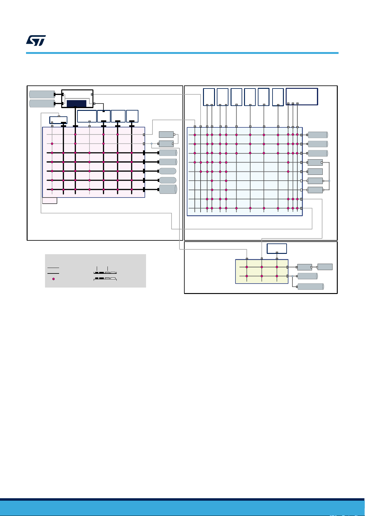
Figure 2. STM32H7 dual‑core system architecture
AN5557
Dual-core system
ITCM-RAM
DTCM-RAM
GPV
Legend
ITCM
L1-Cache
Cortex
(1)
L1-Cache
DTCM
AXIM
ART
D2-to-D1 AHB bus
32-bit bus
64-bit bus
Bus multiplexer
AHBP
®
-M7
AHBS
SDMMC1 MDMA
64-bit AXI bus matrix
D1 Domain
AHB
TCM
AXI
DMA2D
APB
Master interface
Slave interface
LTDC
D1-to-D2 AHB bus
AHB
APB3
AHB
AHB3
AXI
Flash A
AXI
Flash B
AXI
FMC
AXI
QSPI
AXI
AXI
SRAM
APB
D1-to-D3 AHB bus
DMA1
DMA2
DMA1_MEM
DMA2_MEM
DMA2_PERIPH
DMA1_PERIPH
32-bit AHB bus matrix
MAC
Ethernet
SDMMC2
D2 Domain
32-bit AHB bus matrix
D3 Domain
HS1
USB
HS2
USB
D2-to-D1 AHB bus
BDMA
®
Cortex
-M4
I-Bus
D-Bus
S-Bus
SRAM1
SRAM2
SRAM3
AHB1
AHB2
APB1
APB2
D2-to-D3 AHB bus
AHB4
SRAM4
Bckp SRAM
APB
APB4
As illustrated in the Figure 2, the STM32H7 dual‑core devices embed a reduced ART (adaptive real-time) memory
access Accelerator between the D2-to-D1 AHB and the AXI bus matrix. The ART Accelerator is mainly composed
of AHB switch, cache manager and 64 cache lines of 256 bits as shown in Figure 3.
AN5557 - Rev 1
page 6/36
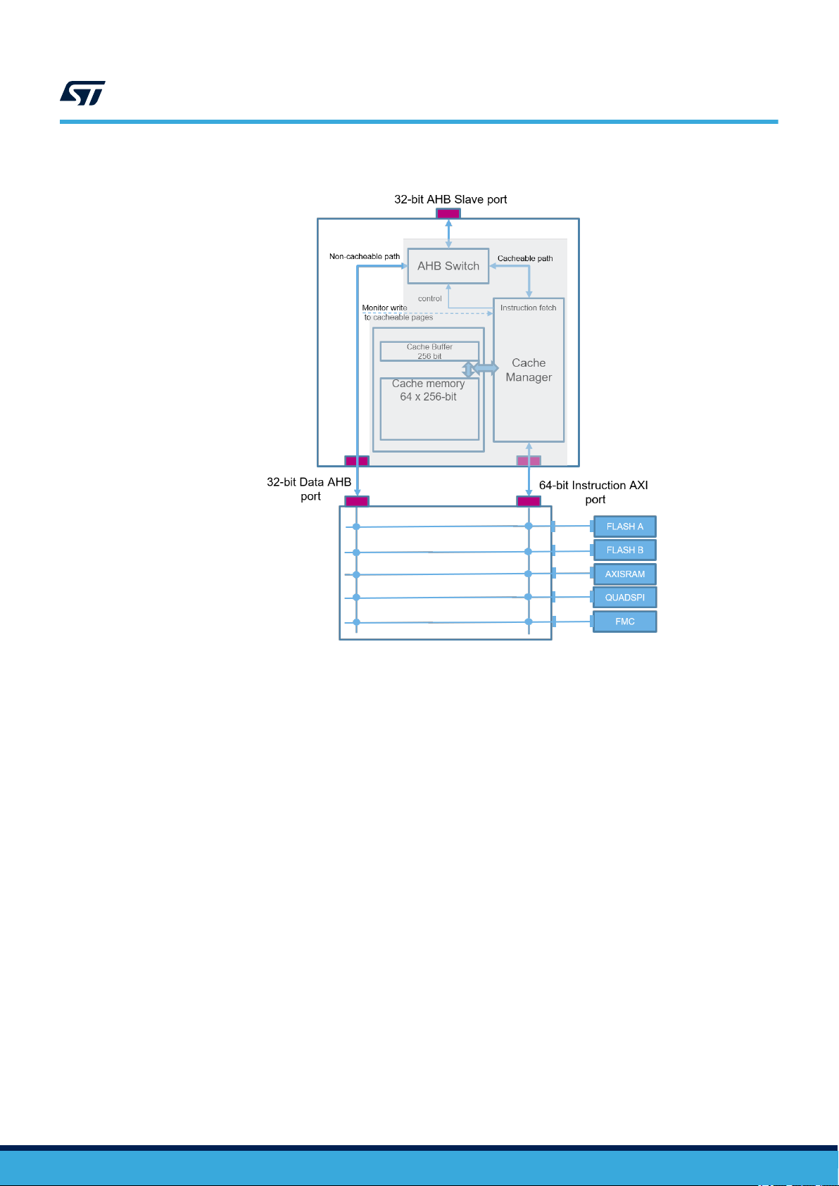
Figure 3. ART block diagram
AN5557
Memory resource assignment
It accelerates cacheable AHB instruction fetch accesses, using a dedicated 64-bit AXI bus matrix port to pre-fetch
code from the internal and external memories of the D1 domain into a built-in cache. It routes all the other AHB
accesses to a dedicated 32-bit AXI bus matrix port connecting the D2-to-D1 AHB with all the internal and external
memories and peripherals of the D1 domain excluding GPV, as well as with the D1-to-D3 AHB. As a consequence
the access of DMAs, Ethernet, except CM4, is always through data 32-bit AHB path.
Note: For more details about ART Accelerator refer to the reference manual RM0399 “STM32H745/755 and
STM32H747/757 advanced Arm®-based 32-bit MCUs”, available from the ST website www.st.com.
2.2
Memory resource assignment
2.2.1 Embedded SRAM
The STM32H7 dual‑core devices feature:
• Up to 864 Kbytes of System SRAM
• 128 Kbytes of data TCM RAM, DTCM RAM
• 64 Kbytes of instruction TCM RAM, ITCM RAM
• 4 Kbytes of backup SRAM
The embedded system SRAM is split into five blocks over the three power domains: AXI SRAM, AHB SRAM1,
AHB SRAM2, AHB SRAM3 and AHB SRAM4.
• D1 domain, AXI SRAM:
– AXI SRAM is accessible through D1 domain AXI bus matrix. It is mapped at address 0x2400 0000 and
accessible by all system masters except BDMA. AXI SRAM can be used for application data which are
not allocated in DTCM RAM or reserved for graphic objects (such as frame buffers)
AN5557 - Rev 1
page 7/36

AN5557
Memory resource assignment
• D2 domain, AHB SRAM:
– AHB SRAM1 is accessible through D2 domain AHB matrix. It is mapped at address 0x3000 0000 and
accessible by all system masters except BDMA. The AHB SRAMs of the D2 domain are also aliased
to an address range below 0x2000 0000 to maintain the Cortex®‑M4 Harvard architecture. The AHB
SRAM1 also mapped at address 0x1000 0000. The AHB SRAM2 also mapped at address 0x1002
0000. The AHB SRAM3 also mapped at address 0x1004 0000. All those AHB SRAMs are accessible
by all system masters through D2 domain AHB matrix. All those AHB SRAMs are accessible by all
system masters through D2 domain AHB matrix.
AHB SRAM1 can be used as DMA buffers to store peripheral input/output data in D2 domain, or as
code location for Cortex®‑M4 CPU (application code available when D1 is powered off). AHB SRAM1
can be used as DMA buffers to store peripheral input/output data in D2 domain, or as code location for
Cortex®‑M4 CPU (application code available when D1 is powered off).
– AHB SRAM2 is accessible through D2 domain AHB matrix. It is mapped at address 0x3002 0000
and accessible by all system masters except BDMA. AHB SRAM2 can be used as DMA buffers to
store peripheral input/output data in D2 domain, or as readwrite segment for application running on
Cortex®‑M4 CPU.
– AHB SRAM3 is accessible through D2 domain AHB matrix is mapped at address 0x3004 0000
and accessible by all system masters except BDMA. AHB SRAM3 can be used as buffers to store
peripheral input/output data for Ethernet and USB, or as shared memory between the two cores.
• D3 domain, AHB SRAM:
– AHB SRAM4 is mapped at address 0x3800 0000 and accessible by most of system masters through
D3 domain AHB matrix. AHB SRAM4 can be used as BDMA buffers to store peripheral input/output
data in D3 domain. It can also be used to retain some application code/data when D1 and D2 domain
in DStandby mode, or as shared memory between the two cores.
The system AHB SRAM can be accessed as bytes, half‑words (16‑bit units) or words (32‑bit units), while the
system AXI SRAM can be accessed as bytes, half‑words, words or doublewords (64‑bit units). These memories
can be addressed at maximum system clock frequency without wait state.
2.2.2 Flash memory
The embedded Flash memory is a central resource for the whole microcontroller. The embedded Flash memory
also proposes a set of security features to protect the assets stored in the non-volatile memory at boot time, at
run-time and during firmware and configuration upgrades.
The embedded Flash memory offers two 64-bit AXI slave ports for code and data accesses, plus a 32-bit AHB
configuration slave port used for register bank accesses. The STM32H7 dual‑core devices embed 2 Mbytes of
Flash memory that can be used for storing programs and data. The Flash memory is organized as 266-bit Flash
words memory that can be used for storing both code and data constants. Each word consists of:
• One Flash word (8 words, 32 bytes or 256 bits)
• 10 ECC bits.
The Flash memory is divided into two independent banks. Each bank is organized as follows:
• 1 Mbyte of user Flash memory block containing eight user sectors of 128 Kbytes (4 K Flash memory words)
• 128 Kbytes of System Flash memory from which the device can boot 2 Kbytes (64 Flash words) of user
option bytes for user configuration
Note: For more details about memory mapping refer to the reference manual RM0399 “STM32H745/755 and
STM32H747/757 advanced Arm
®
‑
based 32‑bit MCUs”, available from the ST website www.st.com.
AN5557 - Rev 1
page 8/36
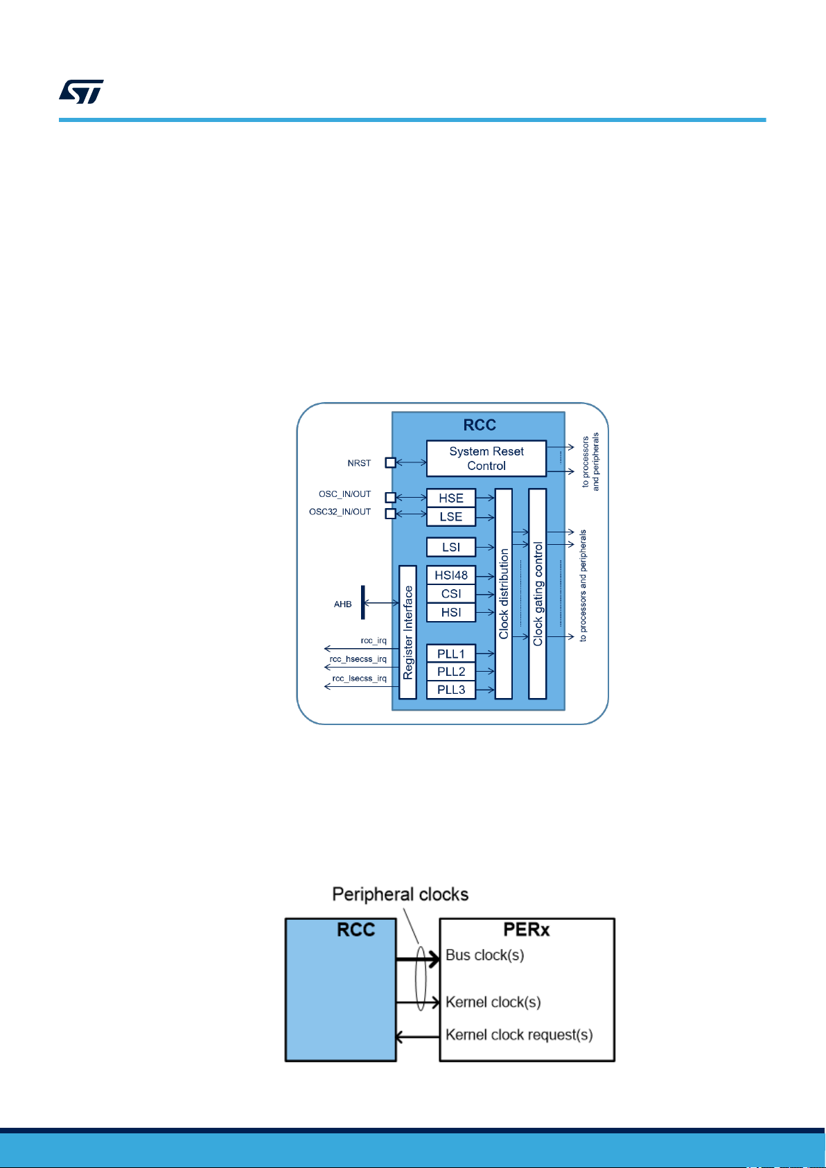
2.3 Peripherals allocation
The peripheral allocation is used by the reset and clock controller (RCC), to automatically control the clock gating
according to the CPUs and domain modes, and by the power controller (PWR) to control the supply voltages
of D1, D2 and D3 domains. As presented in Figure 4. RCC block diagram, the RCC is mainly composed by
the system reset control, the clock distribution, the clock gating control, the register interface, and different clock
sources. The clock gating control is responsible for the peripheral allocation. The RCC manages the reset, the
system and peripheral clocks generation. It uses four internal oscillators, two oscillators for an external crystal or
resonator, and three phase-locked loops (PLL). Therefore, many peripherals have their own clock, independent
of the system clock. The RCC provides high flexibility in the choice of clock sources, which allows the system
designers to meet both power consumption and accuracy requirements. The numerous independent peripheral
clocks allow a designer to adjust the system power consumption without impacting the communication baud rates,
and to keep some peripherals active in low-power mode.
AN5557
Peripherals allocation
Figure 4. RCC block diagram
AN5557 - Rev 1
Many peripheral in STM32H7 dual
bus interface, and the clock for the peripheral specific interface. Generally, the clocks for the data and control
streams via the processor bus interface are named ‘Bus clock’, and the clock for the peripheral specific interface
are named ‘kernel clocks’.
As shown in Figure 5, the peripheral clocks represent the clocks received by the peripheral: ‘bus clock’ and
‘kernel clock’.
‑core, have different clocks for the data and control streams via the processor
Figure 5. Peripheral clock exchange
page 9/36
AN5557
Peripherals allocation
Having a separate bus clock and kernel clock allows the application to change the interconnect and processor
working frequency without affecting the peripheral. For some peripheral it is also possible to disable the bus
clock as long as the peripheral does not need to transfer data to the system. So, it gives a good flexibility on
the frequency selection for the bus processor and memories, and the real need of the peripheral interface. For
example, the UARTs have a kernel clock which is used, among other things, by the baud rate generator for
the serial interface communication, and an APB clock for the register interface. Thus if the system clock has
changed the baud rate is not affected. In addition, some peripherals are able to request the kernel clock when
they detected specific events.
As mentioned before, the peripherals generally receive two types of clocks: bus clock and kernel clock. Those
clocks can be one or several for each peripheral. Each processor can control the clock gating of the peripheral
clocks via dedicated registers located into the RCC.
As illustrated in Figure 6, the gating of the peripheral clocks depends on several parameters:
• The clock enables bits, each processor has a dedicated control bit for that, named C1_PERxEN and
C2_PERxEN
• The low-power clock enables bits : C1_PERxLPEN and C2_PERxLPEN
• The processors states: CRUN, CSLEEP or CSTOP
• The autonomous bits for peripherals located in D3 domain: D3_PERxAMEN
Figure 6. Peripheral clock gating
AN5557 - Rev 1
In Table 2, the operation of peripheral allocation is describing as below:
• When setting the bit C1_PERxEN to ‘1’ indicates that the peripheral PERx is enabled for the CPU1
• When setting the bit C2_PERxEN to ‘1’ indicates that the peripheral PERx is enabled for the CPU2
• When both C1_PERxEN/C2_PERxEN are set, the peripheral clock follows the two CPU states. For
example, if CPU1 is in stop, and CPU2 is in run the clock to the peripheral remains enabled
Table 2. Peripheral clock allocation
CPU1
CRUN CSTOP
CSTOP CRUN
CSTOP CSTOP Disabled
CPU2 Peripheral clock
EnabledCRUN CRUN
page 10/36
It is important to notice that the RCC offers two register sets, allowing each processor to enable or allocate
peripherals. The peripheral allocation informs the RCC that the CPU1 or CPU2 enabled a peripheral. This
information is used by the RCC for the clock control in low-power modes. So before using a peripheral the CPUs
must allocate it. The same peripheral can be allocated by both processors, it is up to the application to avoid
resources conflicts.
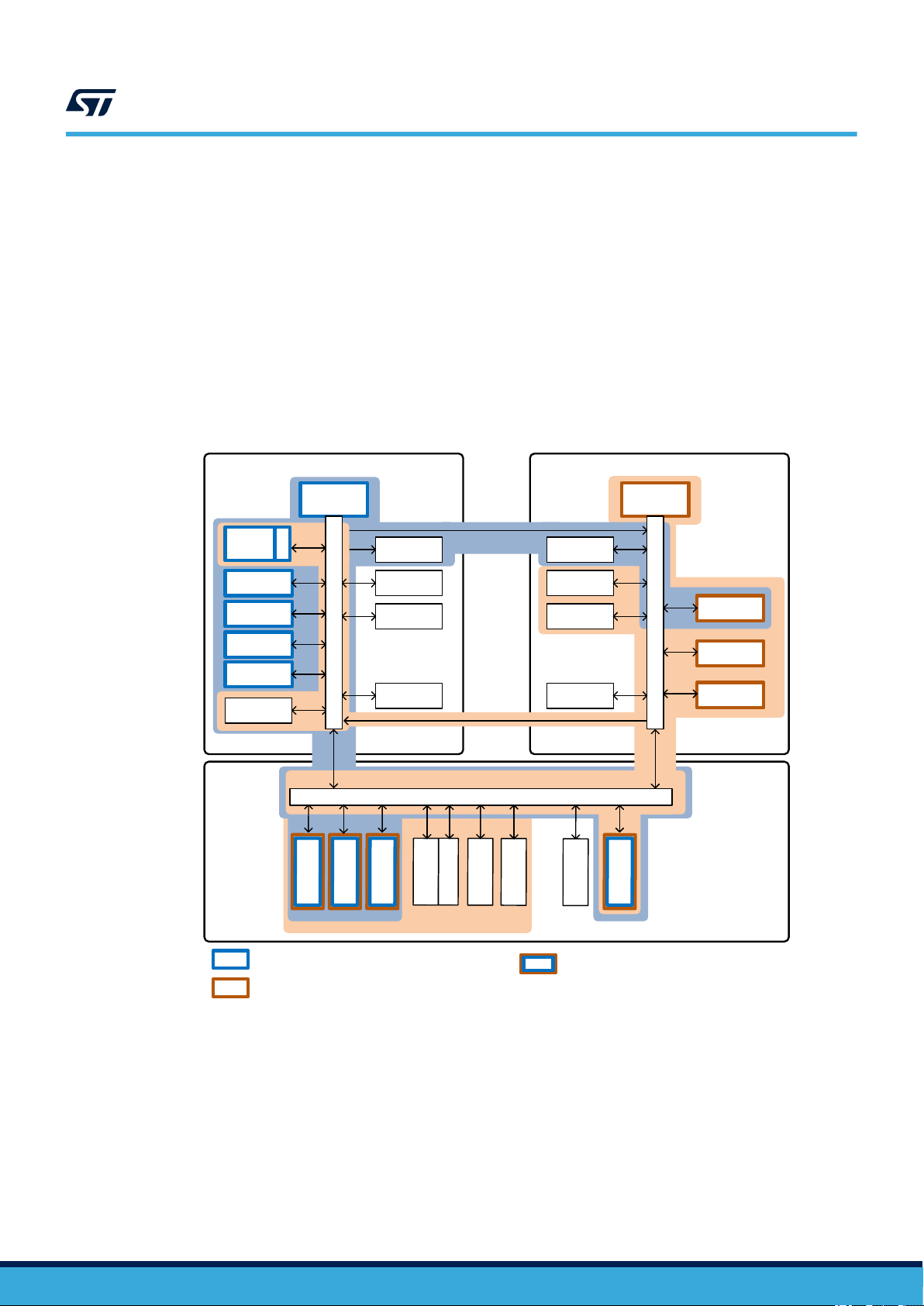
As introduced in the figure below, some peripherals are implicitly allocated to a processor:
• The FLASH, D1SRAM1, ITCM, DTCM1 and DTCM2 are implicitly allocated to CPU1, the CPU2 can allocate
any of them, but by default they are not allocated to CPU2.
• The D2SRAM1, D2SRAM2 and D2SRAM3 are implicitly allocated to CPU2, the CPU1 can allocate any of
them, but by default they are not allocated to CPU1.
Note: Implicitly means architecturally tied to a processor.
Figure 7. Peripheral allocation
AN5557
Peripherals allocation
FLASH
AXISRAM
ITCM
DTCM1
DTCM2
ART
D3
FLITF
D1
CPU1
IWDG1
SDMMC1
PER...
PER...
Bus Matrix 1
PER...
IWDG2
RCC
...
DMA1
CPU1_SS
CPU2_SS
Bus Matrix 3
DMAMUX
I2C4
SAI4
SPI5
SAI1
I2C2
PER...
PER...
...
D2
CPU2
Bus Matrix 2
SRAM1
...
SRAM4
SRAM2
SRAM3
Peripherals implicitly allocated to CPU1
Peripherals implicitly allocated to CPU2
Peripherals implicitly allocated to both
CPUs
Some other peripherals are implicitly allocated to both processors, this is the case for the IWDG1, IWDG2, RCC,
PWR, AIEC and D3SRAM1. When a CPU allocates a peripheral, this peripheral is linked to the processor state
for the low-power modes. The CPU, plus the peripherals allocated by this CPU, and the associated interconnect
is considered by the RCC as a CPU sub-system. The D1 and D2 domain core voltage can be switched-off. To
give a simple example of the use of the peripheral allocation by the RCC, the RCC doesn't allow a domain to
be switched-off, if one of the peripheral of this domain is used by the processor of the other domain which is not
switched-off.
Note: For more details about peripherals allocation, refer to the application note AN5215 “STM32H747/757 advanced
power management”, available from the ST website www.st.com.
AN5557 - Rev 1
page 11/36

2.4 D1 sub-system
The D1 domain is intended for high speed processing and graphics features. Thanks to the AXI bus matrix, this
domain encompasses high bandwidth features and smart management. As shown in the figure below, it contains
the Cortex®‑M7 core running at up to 480 MHz with 16-Kbyte I-cache and 16-Kbyte D-cache, the embedded
memories, the external memories like FMC, Quad-SPI and SD/MMC, the graphic components like JPEG Codec,
DMA2D and LTDC/DSI controller.
The internal memory resources are:
• AXI SRAM (D1 domain) accessible through D1 domain AXI bus matrix:
– AXI SRAM (512-Kbyte) mapped at address 0x2400 0000
– Supports bytes, half-words, full-words or double-words accesses
• ITCM accessible through D1 domain 64-bit ITCM bus
• DTCM accessible through D1 domain 2x32-bit DTCM bus
• Flash memory: two 1MB independent Flash banks
AN5557
D1 sub-system
Figure 8. D1 domain block diagram
AN5557 - Rev 1
page 12/36

2.5 D2 sub-system
The D2 domain is intended for generic peripheral usage (ADC, FDCAN, etc.), communication and data gathering
that it can be processed later in D1 domain. As shown in the figure below, It contains the Cortex®-M4 core running
at up to 240MHz, the embedded memories, the AHB bus matrix, masters like DMA, USB, Ethernet and other
peripherals like FDCAN, UART, SPI, SD/MMC and Timers. Most of the memories dedicated to I/O processing and
most of the peripherals that are less bandwidth demanding. The D2 SRAMs are optimal location for Cortex®-M4
core application data and code. The D2 SRAMs can be used by local DMAs for data transfer from/to peripherals
in this domain. The Data can be transferred to D1 processing domain at end of transfer via MDMA.
AHB SRAM (D2 domain) is accessible through D2 domain AHB matrix:
• AHB SRAM1 (128 KByte) mapped at address 0x3000 0000 and 0x1000 000
• AHB SRAM2 (128 KByte) mapped at address 0x3002 0000 and 0x1002 000
• AHB SRAM3 (32 KByte) mapped at address 0x3004 0000 and 0x1004 000
These memories support bytes, half-words or full-words accesses.
The SRAM1, SRAM2, and SRAM3 can be used for code execution or as buffers to store in/out data of peripherals
located in the D2 domain such as Ethernet and USB. These data can be buffers and descriptors or I2S audio
frames or others.
AN5557
D2 sub-system
Figure 9. D2 domain block diagram
AN5557 - Rev 1
page 13/36

2.6 D3 system domain
The D3 domain provides system management and low power operating modes feature. As shown in
Figure 10. D3 domain block diagram. It contains the embedded memories, the AHB bus matrix, a basic DMA
(BDMA), peripherals like I2C, SPI, ADC, LPTIM, LPUART and system peripherals like RCC, PWR, GPIO. Those
low-power peripherals and memories designed to manage low-power modes. D3 domain is designed to be
autonomous, and embeds a 64-Kbyte RAM, a basic DMA controller (BDMA), plus low-power peripherals to run
basic functions while D1 and D2 domains can be switched off to save power. So, the D3 SRAM can be used to
retain data while the D1 and D2 domains enter DStandby mode.
AHB SRAM (D3 domain) accessible through D3 domain AHB matrix:
• AHB SRAM4 (64 KByte) mapped at address 0x3800 0000 and accessible by most of system masters. It
supports bytes, half-words or full-words accesses.
AN5557
D3 system domain
Figure 10. D3 domain block diagram
AN5557 - Rev 1
page 14/36

3 Resources for dual-core application
3.1 Dual-core communication
When application is running on different CPUs may be independent or cooperating. In many cases they need
mechanisms for:
• Data sharing (events happening)
• Resources sharing and synchronization
The Inter-processors communication (IPC) is the mechanism used by different processors to communicate or
exchange data. These mechanisms ensure safe parallel computation synchronization and application modularity.
This mechanism allows message passing by send and receive messages from other process. It uses a common
memory area with other process. The synchronization with other processors is allowed by semaphores and
interrupts.
There are three possible solutions to be implemented with STM32H7 which are setup communication/
synchronization protocol using the device resources, the FreeRTOS IPC module (from STM32Cube H7 Firmware)
or the OpenAMP framework.
The IPC Module works with FreeRTOS or OS-less application. This module uses the stream buffers to transfer
the data between CPUs and a shared memory region between the core to allocate Stream buffers.
As shown in the figure below, the FreeRTOS IPC module is a set of APIs used by application tasks to exchange
data with a dedicated Stream buffer per Task (only one sender and one receiver).
AN5557
Resources for dual-core application
3.2 Dual-core boot
At startup, the boot memory space is selected by the BOOT pin and BOOT_ADDx option bytes, allowing to
program any boot memory address from 0x0000 0000 to 0x3FFF FFFF which includes all Flash address space,
all RAM address space (ITCM, DTCM RAMs and SRAMs) and the System memory bootloader.
The boot address is provided by option byte and default programmed value to allow:
• CM7 Boots from Flash memory at 0x0800 0000 when Boot0=0
• CM4 Boots from Flash memory at 0x0810 0000 when Boot0=0
• Boot respectively from System memory or SRAM1 when Boot0=1
The values on the BOOT pin are latched on the 4th rising edge of SYSCLK after reset release. It is up to the user
to set the BOOT pin after reset as shown in the figure below.
Figure 11. FreeRTOS IPC block diagram
AN5557 - Rev 1
page 15/36

AN5557
Dual-core boot
Figure 12. Boot selection mechanism
If the programmed boot memory address is out of the memory mapped area or a reserved area, the default boot
fetch address is:
• BCM7_ADD0: FLASH at 0x0800 0000
• BCM4_ADD0: FLASH at 0x0810 0000
• BCM7_ADD1: System Memory at 0x1FF0 0000
• BCM4_ADD1: SRAM1 at 0x1000 0000
When Flash level 2 protection is enabled, only boot from Flash or system is available. If boot address is out
of the memory range or RAM address, then the default fetch is forced from Flash at address 0x0800 0000 for
Cortex®‑M7 and Flash at address 0x0810 0000 for Cortex®-M4. In the STM32H7 dual‑core, to maximize energy
efficiency, each core operates in its own power domain and can be turned off individually when not needed. The
two cores can boot alone or in the same time according to the option bytes as shown in Table 4.
Table 3. Boot order
BCM7
0 0
0 1
1 0
1 1
BCM4 Boot order
Cortex®-M7 is booting and Cortex®-M4 clock is gated
Cortex®-M7 clock is gated and Cortex®-M4 is booting
Cortex®-M7 is booting and Cortex®-M4 clock is gated
Both Cortex®-M7 and Cortex®-M4 are booting
The enabled CPU is defined as the master, it is responsible for system initialization. The other CPU perform
specific initialization. This allows to implement safe booting and proper initialization on power-up.
As shown in Figure 13, three boot cases are provided to build any firmware application where both cores are
used.
The first case is BCM7 = 1 and BCM4 = 0. This is mainly dedicated for parts where CPU1 (Cortex-M7) is booting
and CPU2 (Cortex‑M4) clock is gated. System Init, System clock, voltage scaling and L1-Cache configuration are
done by CPU1 (Cortex-M7) seen as the master CPU. Once done, CPU2 (Cortex-M4) is released through hold
boot function.
The second case is BCM7 = 0 and BCM4 = 1. This is mainly dedicated for parts where CPU2 (Cortex-M4)
is booting and CPU1(Cortex-M7) clock is gated. System Init, System clock and voltage scaling are done by
CPU2(Cortex-M4) seen as the master CPU. Once done, CPU1 (Cortex-M7) is released through hold boot
function which is an RCC feature.
The third case is BCM7 = 1 and BCM4 = 1. This is mainly dedicated for devices where CPU1 (Cortex-M7) and
CPU2 (Cortex-M4) are booting at once. System Init, System clock, voltage scaling and L1-Cache configuration
are done by CPU1 (Cortex-M7). As we do not have to run the System Init twice, the CPU2 (Cortex-M4) can run
another Init needed by the application. Also, customer can choose to use the low power mode and put CPU2
(Cortex-M4) in deep sleep mode by putting Domain D2 in STOP mode to save power consumption.
AN5557 - Rev 1
page 16/36

AN5557
Building example based on STM32CubeMX
Figure 13. Boot mode
Note: For more details about boot mode and boot templates refer to the reference manual RM0399 “STM32H745/755
and STM32H747/757 advanced Arm®-based 32-bit MCUs” and the STM32Cube_FW_H7 firmware, available
from the ST website www.st.com.
3.3 Building example based on STM32CubeMX
The STM32CubeMX is a graphical tool that allows a very easy configuration of STM32 microcontrollers. It
provides the means to configure pin assignments, the clock tree, integrated peripherals, and simulate the power
consumption of the resulting project. It uses a rich library of data from the STM32 microcontrollers portfolio.
The application is intended to ease the initial phase of development, developers to select the best product with
regards to features and power.
AN5557 - Rev 1
page 17/36

3.3.1 Create new project using STM32CubeMX
Run STM32CubeMX tool, the home page appears as shown in the figure below.
Figure 14. STM32CubeMx main screen
AN5557
Building example based on STM32CubeMX
Click on MCU selector access then enter the MCU part number, or the available products can be filtered based on
the specific requirements, as illustrated in the figure below. Then, double click on the chosen product from the list.
Figure 15. MCU selector screen
AN5557 - Rev 1
page 18/36

3.3.2 Pinout configuration
The next step is the peripheral allocation for each CPU which can be applied in the Pinout and Configuration
tab. Then select the peripherals to be used and, where is applicable, assign pins to their inputs and outputs.
Independent GPIOs can also be configured. Signals are assigned to default pins, but they can be transferred to
alternate locations, which are displayed by CTRL-clicking on the pin. For example, when the I2C1 peripheral is
enabled, the tool automatically assigns it to the default pins. We notice in the figure below that some peripherals
are allocated to their default location and are no selectable. Like IWDG1 is in Cortex-M7 and D3 power domain.
Other peripherals, like ADC1 is in D2 power domain but it can be allocated to Cortex-M7 or Cortex-M4. The
tool automatically takes into account the most bonds between the peripherals and the software components it
manages.
AN5557
Building example based on STM32CubeMX
Figure 16. Pinout and configuration screen
AN5557 - Rev 1
page 19/36

3.3.3 Clock configuration
The clock configuration tab provides a schematic overview of the clock paths, along with all clock sources,
dividers, and multipliers. Actual clock speeds are visible. Active and enabled clock signals are highlighted in blue.
Drop-down menus and buttons serve to modify the actual clock configuration. As shown in Figure 17, for example
it can chose the PLLCLK clock source in the System Clock Mux to generate the clock to Cortex-M7 (CPU1)
and Cortex-M4 (CPU2) clocks. If a configured value is out of specification, it immediately turns red to highlight a
problem. It also works the other way; enter the required clock speed in a blue frame and the software attempts to
reconfigure multipliers and dividers to provide the requested value. Right-click on a clock value in blue and select
"lock" to lock it to prevent modifications.
AN5557
Building example based on STM32CubeMX
Figure 17. Clock configuration screen
AN5557 - Rev 1
page 20/36

3.3.4 Project configuration and code generation
As introduced in Figure 18, switch to the Project manager tab, then select Project to fill Project Name, Project
Location fields and select the suitable Toolchain/IDE. The user can click on Code Generator or Advanced Settings
to change for example the generated files settings.
Figure 18. Project manager screen
AN5557
Building example based on STM32CubeMX
When all inputs, outputs, and peripherals are configured, the code is ready to be generated by clicking on
GENERATE CODE.
AN5557 - Rev 1
page 21/36

3.3.5 Power consumption calculator
Click on Tools tab to find the Power consumption calculator, as illustrated in Figure 19. This configuration
pane is mostly informative, summarizing the selected MCU and the default power source. Parameters such
as temperature and voltage may even be defined, depending on the MCU selected and the available power
consumption data. The Battery selection pane is used to select or define a battery type. The battery source
is optional and, if defined, may be used in only selected sequence steps, simulating a device that works both
independently and connected to an external power source. Information and help sections include useful notes
for the user. In PCC tab click on New Step, select the system power mode, the domain CPU power mode, the
memory fetch type and other preferences adequate with his application.
AN5557
Debugging the multicore application
Figure 19. PCC screen
Note: Note: For more information about STM32CubeMx configuration refer to User Manual UM1718 “STM32CubeMX
for STM32 configuration and initialization C code generation” available from the ST website www.st.com.
3.4
Debugging the multicore application
The debug can be controlled via a JTAG/Serial-wire debug access port, using industry standard debugging tools.
The debug infrastructure allows debugging one core at a time, or both cores in parallel. The trace port performs
data capture for logging and analysis. A 4-Kbyte embedded trace FIFO (ETF) allows recording data and sending
them to any com port. In Trace mode, the trace is transferred by DMA to system RAM or to a high-speed interface
(such as SPI or USB). It can even be monitored by a software running on one of the cores. Unlike hardware FIFO
mode, this mode is invasive since it uses system resources which are shared by the processors.
The devices offer a comprehensive set of debug and trace features on both cores to support software
development and system integration:
• Breakpoint debugging
• Code execution tracing
• Software instrumentation
• JTAG debug port
• Serial-wire debug port
• Trigger input and output
• Serial-wire trace port
• Trace port
•
Arm® CoreSight™ debug and trace components
AN5557 - Rev 1
page 22/36

AN5557
Debugging the multicore application
The debug components are distributed across the power domains D1 , D2 and D3 as illustrated in the figure
below.
Figure 20. Block diagram of the device debug
3.4.1 Embedded trace macrocell (ETM)
The Real-time trace module providing instruction trace of a processor. As shown in the figure below, the
ETM is used with the TPIU comprising a clock and four data outputs TRACECLK, four data outputs and
TRACEDATA(3:0).
Figure 21. Block diagram of ETM debug
AN5557 - Rev 1
page 23/36

3.4.2 Instrumentation trace macrocell (ITM)
The ITM is a CoreSight™ block that generates trace information into packets, as illustrated in the figure below.
The following sources of the ITM trace packet are:
• Software trace. Software can write directly to ITM stimulus registers to generate packets.
• Hardware trace. The DWT generates these packets, and the ITM outputs them.
• Local Time stamping: Provides timing information on the ITM trace packets
• Global Time stamping: generated using the system-wide 64-bit count value coming from the Timestamp
Generator component
Figure 22. Block diagram of ITM debug
AN5557
Debugging the multicore application
3.4.3 Data watchpoint trace (DWT)
The DWT is a CoreSight™ component that provides watchpoints, data tracing, and system profiling for the
processor, as presented in the figure below.
The main components of the DWT are Data watchpoint and data tracing. It is responsible for:
• Halt the core when a memory area is accessed (Read, Write or both)
• Send data address and/or PC via ITM
• ETM Trigger
It also contains Counters for Clock cycles, Folded instructions, load store unit (LSU), Sleep cycles and number of
cycles per instruction.
3.4.4 Trace funnel (CSTF)
The trace funnel (CSTF) is a CoreSight™ component that combines the four trace sources into one single ATB.
The CSTF has four ATB slave ports, and one ATB master port. An arbiter selects the slave ports according to a
programmable priority. This slave ports are connected as follows:
• S0: Cortex-M7 ETM
• S1: Cortex-M7 ITM
• S2: Cortex-M4 ETM
• S3: Cortex-M4 ITM
The trace funnel registers allow the slave ports to be individually enabled, and their priority settings to be
configured. The priorities can be modified only when trace is disabled.
Figure 23. Block diagram of DWT debug
AN5557 - Rev 1
page 24/36

3.4.5 Cross trigger interfaces (CTI)
The Cross-Trigger Interfaces is a CoreSight™ component. As introduced in the figure below, it enables the
debug logic and ETM to interact with each other and with other components of the CoreSight™. It allows cores
synchronization (Run/Halt) and triggers for the traces modules.
3.4.6 Embedded trace FIFO (ETF)
The ETF is an 8-kbyte memory which captures trace data from four trace sources, namely the ETM and ITM of
each CPU core. Once the trace stopped, the buffer can be read out via three methods:
• The Trace Port: with the TPIU enabled, the contents of the buffer are output over the trace port
• The debugger via the Debug Port
• One of the cores
AN5557
Debugging the multicore application
Figure 24. Block diagram of CTI debug
3.4.7 Microcontroller debug unit (DBGMCU)
The DBGMCU is not a CoreSight™ component and the DBGMCU registers are not reset by system reset but only
by power on reset.
The main functionalities of the DBGMCU unit are:
• Emulated low power mode: Maintain the clock to the processor and debug component active in low power
mode
• Stop the clock to certain peripherals when either processor is stopped in debug mode
• DBGMCU registers are accessible to the debugger via the APB-D bus at base address 0xE00E1000 and by
both processor cores at base address 0x5C001000
Note: For more details about STM32H7 dual‑core debugging refer to the application note AN5286 “STM32H7x5/x7
dual-core microcontroller debugging” available from the ST website www.st.com.
AN5557 - Rev 1
page 25/36

4 Application partitioning examples
As shown in the figure below, the device can be divided in three main blocks. The D1 domain provides processing
and graphics features. The D2 domain provides peripheral management. The D3 domain provides system
management and low power operating modes feature. The dual‑core synchronization and communication is
managed by the Inter-Processor Communication layer.
Figure 25. STM32H7 dual‑core functional partitioning
AN5557
Application partitioning examples
4.1
Dual-core application design considerations
The dual‑core application design considerations can be divided in three main parts which are system design
considerations, software design considerations and dual-core application design.
The system design considerations are mainly based on four methodologies. First, the processors and domains
resources assignment to different tasks, second the memory mapping, then the interrupts distribution and the
inter-processor communication/ synchronization.
The software design considerations are based on three process, which are task partitioning, data sharing and
overheads avoidance. First, the task partitioning should allow dependencies/ concurrency reduction and avoid
overheads that limit execution time benefits. Then, the Data sharing that use a proper data layout in memory to
minimize overhead and respect dependency relationships for data synchronization and coherency. Finally, avoid
overheads by maximizing data locality and minimizing contention and wait for resources.
The dual-core application design consist in three principal steps:
• The first step is to analyze the serial implementation bottleneck and identify the part of the program to
improve.
• The second step is to set the critical application requirements to meet performance/power compromise.
• The third step is to identify the appropriate parallel design, it can be a fully independent tasks or
collaborating tasks.
AN5557 - Rev 1
page 26/36

4.2 Task partitioning schema
The main task partitioning schema are the parallel partitioning, the data processing partitioning, and the pipelined
partitioning.
The task parallel partitioning is used when tasks can be decomposed into independent sub-tasks and then
allocated to a CPU for execution, as illustrated in Figure 26. Task parallel partitioning. Those tasks are executed
concurrently on either the same or different sets of data. The parallelization of the design is related to the number
of independent tasks.
AN5557
Task partitioning schema
Figure 26. Task parallel partitioning
The data processing partitioning is used when different subsets of the same data can be processed in parallel
by the two CPUs, as illustrated in Figure 27. This partition is relevant for regular data structures like arrays and
matrices because it is easy to handle each element in parallel. It focuses on distributing the data across the
CPUs, which operate on the data in parallel. The parallelization of the design is related to data input size.
Figure 27. Data processing partitioning
The pipelined partitioning allows the execution of multiple instructions on the same data, which is allocated on
different CPUs, as shown in Figure 28. This partitioning split up the processing into stages and each stage
operate a specific part of the algorithm at a time, the output of one stage is the input of the next stage.
Figure 28. Pipelined partitioning
AN5557 - Rev 1
page 27/36

Example 1: JPEG images streaming over network
4.3 Example 1: JPEG images streaming over network
The application tasks can be split on the two CPUs, As shown in the figure below. The JPEG images transfer task
allocated to CPU1 and the Covert RGB to YCbCr task allocated to CPU2. The peripheral resources used by this
application are Flash, AXISRAM, SRAMs, DCMI, DMA1, MDMA and Ethernet.
Figure 29. Task partition of example 1
AN5557
The peripheral allocation informs the RCC that a CPU enabled a peripheral. This information is used for
low-power modes and the allocated peripheral remains accessible to the second CPU. In addition to implicitly
allocated peripherals for example Flash or AXISRAM, additional resources need to be allocated depending on
application needs (JPEG HW codec, MDMA, DMAs, DCMI…). For shared resources like SRAM1 or AXISRAM a
software protection might be required to avoid data corruption, the use of memory protection unit (MPU) regions
can be defined to isolate data and peripherals tasks.
The user must take care about Data coherency between CM7 and CM4. This is done either by cache
maintenance or configure the shared memory as non-cachable memory.
The CPU2 can offload CPU1 from tasks such as image acquisition and image pre-processing. To enhance
performance, designers should maximize data locality by using D2 SRAMs for CPU2, managing data transfers
and encoding via DMAs (DMA1/MDMA) and JPEG HW codec. Also, the DMA can offload CPU2 when acquiring
data from DCMI interface and the MDMA can fetch data from D2 SRAM to encode them via JPEG HW codec.
Then, the encoded images is streamed over Ethernet.
Note: For more details about data coherency, refer to AN4839 "Level 1 cache on STM32F7 Series and STM32H7
Series" available from ST website .
AN5557 - Rev 1
page 28/36

Example 2: Sensor data acquisition and data streaming to cloud
4.4 Example 2: Sensor data acquisition and data streaming to cloud
The application tasks may be split over the two CPUs, As shown in the figure below. In addition, those tasks
can be divided in two modes: active mode and low power mode. The user interface management is allocated to
CPU1. The sensors management and Data logging to cloud are allocated to CPU2. The sensors management
is allocated to low power autonomous D3 domain. The peripheral resources used by this application are Flash,
AXISRAM, SRAMs, SPI/I2C, LTDC/DSI, DMA2D, DMA, BDMA, Ethernet and FMC.
Figure 30. Task partition of example 2
AN5557
4.5
The allocated graphical sub-system to CPU1 are LTDC/DSI, DMA2D and FMC. The Ethernet, and Flash are
allocated to CPU2. The BDMA and sensor management interfaces (SPI, I2C…) should be allocated to D3
autonomous mode.
In order to enhance power consumption, Flash allocation to CPU2 can be released (refer to
Section 2.3 Peripherals allocation) when it is not used to allow D1 domain to switch OFF clock and power.
The CPU1 may be overloaded by computationally intensive operation like encryptions and communication to
cloud, in this case CPU2 ensure responsiveness by isolating user interface from time-consuming tasks to offload
CPU1.
To enhance power consumption, the dependencies between domains should be reduced as domains can be
independently switched OFF. For example, D1 domain resources are mainly used by CPU1 for user interface
management, D1 may be switched OFF if CPU1 is in low power mode. D1 and D2 domains can be switched OFF
while sensors can be managed by D3 in autonomous mode. Also, a proper data mapping can reduce the need to
move data from one memory to another like sensor data mapping in SRAM4.
Example 3: Motor control and real-time communication
The application tasks can be split on the two CPUs, As shown in the figure below. The Motor control is allocated
to CPU1. The real-time communication is allocated to CPU2. The peripheral resources used by this application
are Flash, AXISRAM, SRAMs, TIMERs, CAN, UART, ADCs/DFSDM, DMAs and Ethernet.
Figure 31. Task partition of example 3
AN5557 - Rev 1
The allocated motor control sub-system to CPU1 are DMA1, DFSDM, TIMERs and SRAM1. The allocate
communication sub-system to CPU2 are DMA2, USART, FDCAN and Ethernet. Designers should avoid resources
sharing between application to reduce wait time for resource availability. For example, DMA1 is allocated to CPU1
and DMA2 is allocated for CPU2.
It is possible to isolate time critical tasks from other tasks by making them independently running on a different
processor. For example, the MPU configuration can be set on the two processors to avoid data corruption.
page 29/36

5 Conclusion
The STM32H7 dual-core embedded the Arm® Cortex®-M7 and the Cortex®-M4 32-bit RISC cores running up to
480 MHz and up to 240 MHz respectively. Those STM32H7 dual-core microcontrollers are more powerful and
offer high flexible architecture than predecessors in STM32H7 Series. It provides more processing and open
application partitioning. To get benefits from the two CPUs, the system architecture incorporates instruction and
data cache for Cortex®-M7 and Adaptive real-time accelerator for Cortex®-M4. Also, it allows high-performance
tasks execution while optimizing the overall power consumption. Each core belongs to independent power
domain, this provides safe boot modes and enhance the power consumption significantly.
This application note has shown the system architecture of the STM32H7 dual-core, which is split in three power
domains. In addition, it presents the memory resources and how it can be accessible by the cores and other
masters. Besides, it introduces the peripheral allocation for each CPU and shown an example of this process
through STM32CubeMx tool. Moreover, it reveales the dual-core design consideration and provides resources
partitioning based on some applicative examples.
AN5557
Conclusion
AN5557 - Rev 1
page 30/36

Revision history
AN5557
Table 4. Document revision history
Date Version Changes
13-Nov-2020 1 Initial release
AN5557 - Rev 1
page 31/36

AN5557
Contents
Contents
1 General information ...............................................................2
2 System overview ..................................................................3
2.1 Dual-core system ..............................................................4
2.2 Memory resource assignment ....................................................7
2.2.1 Embedded SRAM ........................................................7
2.2.2 Flash memory ...........................................................8
2.3 Peripherals allocation ...........................................................9
2.4 D1 sub-system................................................................12
2.5 D2 sub-system................................................................13
2.6 D3 system domain ............................................................14
3 Resources for dual-core application ..............................................15
3.1 Dual-core communication.......................................................15
3.2 Dual-core boot ...............................................................15
3.3 Building example based on STM32CubeMX .......................................17
3.3.1 Create new project using STM32CubeMX ....................................18
3.3.2 Pinout configuration .....................................................19
3.3.3 Clock configuration ......................................................20
3.3.4 Project configuration and code generation ....................................21
3.3.5 Power consumption calculator .............................................22
3.4 Debugging the multicore application..............................................22
3.4.1 Embedded trace macrocell (ETM)...........................................23
3.4.2 Instrumentation trace macrocell (ITM) ........................................24
3.4.3 Data watchpoint trace (DWT) ..............................................24
3.4.4 Trace funnel (CSTF) .....................................................24
3.4.5 Cross trigger interfaces (CTI) ..............................................25
3.4.6 Embedded trace FIFO (ETF)...............................................25
3.4.7 Microcontroller debug unit (DBGMCU) .......................................25
4 Application partitioning examples.................................................26
4.1 Dual-core application design considerations .......................................26
4.2 Task partitioning schema.......................................................27
AN5557 - Rev 1
page 32/36

AN5557
Contents
4.3 Example 1: JPEG images streaming over network..................................28
4.4 Example 2: Sensor data acquisition and data streaming to cloud......................29
4.5 Example 3: Motor control and real-time communication .............................29
5 Conclusion ......................................................................30
Revision history .......................................................................31
Contents ..............................................................................32
List of tables ..........................................................................34
List of figures..........................................................................35
AN5557 - Rev 1
page 33/36

AN5557
List of tables
List of tables
Table 1. Bus-master-to-slave interconnection....................................................... 5
Table 2. Peripheral clock allocation............................................................. 10
Table 3. Boot order........................................................................ 16
Table 4. Document revision history .............................................................31
AN5557 - Rev 1
page 34/36

AN5557
List of figures
List of figures
Figure 1. STM32H7 dual‑core block diagram ......................................................3
Figure 2. STM32H7 dual‑core system architecture ..................................................6
Figure 3. ART block diagram .................................................................7
Figure 4. RCC block diagram .................................................................9
Figure 5. Peripheral clock exchange ............................................................9
Figure 6. Peripheral clock gating ............................................................. 10
Figure 7. Peripheral allocation ............................................................... 11
Figure 8. D1 domain block diagram ........................................................... 12
Figure 9. D2 domain block diagram ........................................................... 13
Figure 10. D3 domain block diagram ........................................................... 14
Figure 11. FreeRTOS IPC block diagram ........................................................ 15
Figure 12. Boot selection mechanism ...........................................................16
Figure 13. Boot mode ...................................................................... 17
Figure 14. STM32CubeMx main screen ......................................................... 18
Figure 15. MCU selector screen............................................................... 18
Figure 16. Pinout and configuration screen ....................................................... 19
Figure 17. Clock configuration screen ........................................................... 20
Figure 18. Project manager screen............................................................. 21
Figure 19. PCC screen .....................................................................22
Figure 20. Block diagram of the device debug ..................................................... 23
Figure 21. Block diagram of ETM debug ......................................................... 23
Figure 22. Block diagram of ITM debug.......................................................... 24
Figure 23. Block diagram of DWT debug......................................................... 24
Figure 24. Block diagram of CTI debug .......................................................... 25
Figure 25. STM32H7 dual‑core functional partitioning ................................................26
Figure 26. Task parallel partitioning ............................................................ 27
Figure 27. Data processing partitioning .......................................................... 27
Figure 28. Pipelined partitioning............................................................... 27
Figure 29. Task partition of example 1 ........................................................... 28
Figure 30. Task partition of example 2 ........................................................... 29
Figure 31. Task partition of example 3 ........................................................... 29
AN5557 - Rev 1
page 35/36

AN5557
IMPORTANT NOTICE – PLEASE READ CAREFULLY
STMicroelectronics NV and its subsidiaries (“ST”) reserve the right to make changes, corrections, enhancements, modifications, and improvements to ST
products and/or to this document at any time without notice. Purchasers should obtain the latest relevant information on ST products before placing orders. ST
products are sold pursuant to ST’s terms and conditions of sale in place at the time of order acknowledgement.
Purchasers are solely responsible for the choice, selection, and use of ST products and ST assumes no liability for application assistance or the design of
Purchasers’ products.
No license, express or implied, to any intellectual property right is granted by ST herein.
Resale of ST products with provisions different from the information set forth herein shall void any warranty granted by ST for such product.
ST and the ST logo are trademarks of ST. For additional information about ST trademarks, please refer to www.st.com/trademarks. All other product or service
names are the property of their respective owners.
Information in this document supersedes and replaces information previously supplied in any prior versions of this document.
© 2020 STMicroelectronics – All rights reserved
AN5557 - Rev 1
page 36/36
 Loading...