

STMicroelectronics STM32H725ZE, STM32H725VE, STM32H725RE, STM32H725IE, STM32H725AE Datasheet
...
STM32H725xE/G
VFQFPN 68
(8x8 mm)
W
L
C
S
P
1
1
5
0
.
3
5
m
m
p
i
t
c
h
FBGA
TFBGA100
(8x8 mm)
LQFP100 (14 x 14 mm)
LQFP144 (20 x 20 mm)
LQFP176 (24 x 24 mm)
FBGA
UFBGA 169 (7 x 7 mm)
UFBGA 176+25 (10 x 10 mm)
32-bit Arm® Cortex®-M7 550 MHz MCU, up to 1 MB Flash memory,
564 KB RAM, 35 comms peripherals and analog interfaces
Datasheet - production data
Features
Core
• 32-bit Arm® Cortex®-M7 CPU with DP-FPU, L1
cache: 32-Kbyte data cache and 32-Kbyte
instruction cache allowing 0-wait state
execution from embedded Flash memory and
external memories, frequency up to 550 MHz,
MPU, 1177 DMIPS/2.14 DMIPS/MHz
(Dhrystone 2.1), and DSP instructions
Memories
• Up to 1 Mbyte of embedded Flash memory with
ECC
• SRAM: total 564 Kbytes all with ECC, including
128 Kbytes of data TCM RAM for critical realtime data + 432 Kbytes of system RAM (up to
256 Kbytes can remap on instruction TCM
RAM for critical real time instructions) +
4 Kbytes of backup SRAM (available in the
lowest-power modes)
• Flexible external memory controller with up to
24-bit data bus: SRAM, PSRAM,
SDRAM/LPSDR SDRAM, NOR/NAND
memories
• 2 x Octo-SPI interface with XiP
• 2 x SD/SDIO/MMC interface
• Bootloader
Graphics
Clock, reset and supply management
• 1.62 V to 3.6 V application supply and I/O
• POR, PDR, PVD and BOR
• Dedicated USB power
• Embedded DCDC and LDO regulator
(*)VFQFPN68 variant is DCDC only
• Internal oscillators: 64 MHz HSI, 48 MHz
HSI48, 4 MHz CSI, 32 kHz LSI
• External oscillators: 4-50 MHz HSE,
32.768 kHz LSE
• Chrom-ART Accelerator graphical hardware
• LCD-TFT controller supporting up to XGA
September 2020 DS13311 Rev 2 1/276
accelerator enabling enhanced graphical user
interface to reduce CPU load
resolution
Low power
• Sleep, Stop and Standby modes
• V
supply for RTC, 32×32-bit backup
BAT
registers
Analog
• 2×16-bit ADC, up to 3.6 MSPS in 16-bit: up to
22 channels and 7.2 MSPS in doubleinterleaved mode
www.st.com

STM32H725xE/G
• 1 x 12-bit ADC, up to 5 MSPS in 12-bit, up to 12
channels
• 2 x comparators
• 2 x operational amplifier GBW = 8 MHz
• 2× 12-bit D/A converters
Digital filters for sigma delta modulator
(DFSDM)
• 8 channels/4 filters
4 DMA controllers to offload the CPU
• 1 × MDMA with linked list support
• 2 × dual-port DMAs with FIFO
• 1 × basic DMA with request router capabilities
24 timers
• Seventeen 16-bit (including 5 x low power
16-bit timer available in stop mode) and four
32-bit timers, each with up to 4 IC/OC/PWM or
pulse counter and quadrature (incremental)
encoder input
• 2x watchdogs, 1x SysTick timer
external clock and up to 5 x SPI (from 5 x
USART when configured in synchronous
mode)
• 2x SAI (serial audio interface)
• 1× FD/TT-CAN and 2xFD-CAN
• 8- to 14-bit camera interface
• 16-bit parallel slave synchronous interface
• SPDIF-IN interface
• HDMI-CEC
• Ethernet MAC interface with DMA controller
• USB 2.0 high-speed/full-speed
device/host/OTG controller with dedicated
DMA, on-chip FS PHY and ULPI for external
HS PHY
• SWPMI single-wire protocol master I/F
• MDIO slave interface
Mathematical acceleration
• CORDIC for trigonometric functions
acceleration
• FMAC: Filter mathematical accelerator
Debug mode
• SWD and JTAG interfaces
• 2-Kbyte embedded trace buffer
Up to 128 I/O ports with interrupt
capability
Up to 35 communication interfaces
• Up to 5 × I2C FM+ interfaces
(SMBus/PMBus™)
• Up to 5 USARTs/5 UARTs (ISO7816 interface,
LIN, IrDA, modem control) and 1 x LPUART
• Up to 6 SPIs with 4 with muxed duplex I2S for
audio class accuracy via internal audio PLL or
Table 1. Device summary
Reference Part number
STM32H725xE
STM32H725xG
STM32H725ZE, STM32H725VE, STM32H725RE, STM32H725IE,
STM32H725AE
STM32H725ZG, STM32H725VG, STM32H725RG, STM32H725IG,
STM32H725AG
Digital temperature sensor
True random number generator
CRC calculation unit
RTC with sub-second accuracy and
hardware calendar
ROP, PC-ROP, tamper detection
96-bit unique ID
All packages are ECOPACK2 compliant
2/276 DS13311 Rev 2

STM32H725xE/G Contents
Contents
1 Introduction . . . . . . . . . . . . . . . . . . . . . . . . . . . . . . . . . . . . . . . . . . . . . . . 14
2 Description . . . . . . . . . . . . . . . . . . . . . . . . . . . . . . . . . . . . . . . . . . . . . . . . 15
3 Functional overview . . . . . . . . . . . . . . . . . . . . . . . . . . . . . . . . . . . . . . . . 23
3.1 Arm® Cortex®-M7 with FPU . . . . . . . . . . . . . . . . . . . . . . . . . . . . . . . . . . . 23
3.2 Memory protection unit (MPU) . . . . . . . . . . . . . . . . . . . . . . . . . . . . . . . . . 23
3.3 Memories . . . . . . . . . . . . . . . . . . . . . . . . . . . . . . . . . . . . . . . . . . . . . . . . . 24
3.3.1 Embedded Flash memory . . . . . . . . . . . . . . . . . . . . . . . . . . . . . . . . . . . 24
3.3.2 Embedded SRAM . . . . . . . . . . . . . . . . . . . . . . . . . . . . . . . . . . . . . . . . . 24
Error code correction (ECC) . . . . . . . . . . . . . . . . . . . . . . . . . . . . . . . . . . . . . . . . .25
3.4 Boot modes . . . . . . . . . . . . . . . . . . . . . . . . . . . . . . . . . . . . . . . . . . . . . . . 26
3.5 CORDIC co-processor (CORDIC) . . . . . . . . . . . . . . . . . . . . . . . . . . . . . . 26
CORDIC features . . . . . . . . . . . . . . . . . . . . . . . . . . . . . . . . . . . . . . . . . . . . . . . . .26
3.6 Filter mathematical accelerator (FMAC) . . . . . . . . . . . . . . . . . . . . . . . . . . 27
FMAC features . . . . . . . . . . . . . . . . . . . . . . . . . . . . . . . . . . . . . . . . . . . . . . . . . . .27
3.7 Power supply management . . . . . . . . . . . . . . . . . . . . . . . . . . . . . . . . . . . 27
3.7.1 Power supply scheme . . . . . . . . . . . . . . . . . . . . . . . . . . . . . . . . . . . . . . 27
3.7.2 Power supply supervisor . . . . . . . . . . . . . . . . . . . . . . . . . . . . . . . . . . . . 29
3.7.3 Voltage regulator . . . . . . . . . . . . . . . . . . . . . . . . . . . . . . . . . . . . . . . . . . 30
3.8 Low-power strategy . . . . . . . . . . . . . . . . . . . . . . . . . . . . . . . . . . . . . . . . . 30
3.9 Reset and clock controller (RCC) . . . . . . . . . . . . . . . . . . . . . . . . . . . . . . . 31
3.9.1 Clock management . . . . . . . . . . . . . . . . . . . . . . . . . . . . . . . . . . . . . . . . 31
3.9.2 System reset sources . . . . . . . . . . . . . . . . . . . . . . . . . . . . . . . . . . . . . . 32
3.10 General-purpose input/outputs (GPIOs) . . . . . . . . . . . . . . . . . . . . . . . . . . 32
3.11 Bus-interconnect matrix . . . . . . . . . . . . . . . . . . . . . . . . . . . . . . . . . . . . . . 32
3.12 DMA controllers . . . . . . . . . . . . . . . . . . . . . . . . . . . . . . . . . . . . . . . . . . . . 34
3.13 Chrom-ART Accelerator (DMA2D) . . . . . . . . . . . . . . . . . . . . . . . . . . . . . . 34
3.14 Nested vectored interrupt controller (NVIC) . . . . . . . . . . . . . . . . . . . . . . . 35
3.15 Extended interrupt and event controller (EXTI) . . . . . . . . . . . . . . . . . . . . 35
3.16 Cyclic redundancy check calculation unit (CRC) . . . . . . . . . . . . . . . . . . . 35
3.17 Flexible memory controller (FMC) . . . . . . . . . . . . . . . . . . . . . . . . . . . . . . 36
3.18 Octo-SPI memory interface (OCTOSPI) . . . . . . . . . . . . . . . . . . . . . . . . . 36
DS13311 Rev 2 3/276
8

Contents STM32H725xE/G
3.19 Analog-to-digital converters (ADCs) . . . . . . . . . . . . . . . . . . . . . . . . . . . . . 37
3.20 Temperature sensor . . . . . . . . . . . . . . . . . . . . . . . . . . . . . . . . . . . . . . . . . 37
3.21 Digital temperature sensor (DTS) . . . . . . . . . . . . . . . . . . . . . . . . . . . . . . . 37
3.22 V
operation . . . . . . . . . . . . . . . . . . . . . . . . . . . . . . . . . . . . . . . . . . . . . 38
BAT
3.23 Digital-to-analog converters (DAC) . . . . . . . . . . . . . . . . . . . . . . . . . . . . . 38
3.24 Ultra-low-power comparators (COMP) . . . . . . . . . . . . . . . . . . . . . . . . . . . 39
3.25 Operational amplifiers (OPAMP) . . . . . . . . . . . . . . . . . . . . . . . . . . . . . . . 39
3.26 Digital filter for sigma-delta modulators (DFSDM) . . . . . . . . . . . . . . . . . . 40
3.27 Digital camera interface (DCMI) . . . . . . . . . . . . . . . . . . . . . . . . . . . . . . . . 42
3.28 PSSI . . . . . . . . . . . . . . . . . . . . . . . . . . . . . . . . . . . . . . . . . . . . . . . . . . . . . 42
3.29 LCD-TFT controller . . . . . . . . . . . . . . . . . . . . . . . . . . . . . . . . . . . . . . . . . . 42
3.30 True random number generator (RNG) . . . . . . . . . . . . . . . . . . . . . . . . . . 43
3.31 Timers and watchdogs . . . . . . . . . . . . . . . . . . . . . . . . . . . . . . . . . . . . . . . 44
3.31.1 Advanced-control timers (TIM1, TIM8) . . . . . . . . . . . . . . . . . . . . . . . . . 46
3.31.2 General-purpose timers (TIMx) . . . . . . . . . . . . . . . . . . . . . . . . . . . . . . . 46
3.31.3 Basic timers TIM6 and TIM7 . . . . . . . . . . . . . . . . . . . . . . . . . . . . . . . . . 47
3.31.4 Low-power timers (LPTIM1, LPTIM2, LPTIM3, LPTIM4, LPTIM5) . . . . 47
3.31.5 Independent watchdog . . . . . . . . . . . . . . . . . . . . . . . . . . . . . . . . . . . . . 47
3.31.6 Window watchdog . . . . . . . . . . . . . . . . . . . . . . . . . . . . . . . . . . . . . . . . . 47
3.31.7 SysTick timer . . . . . . . . . . . . . . . . . . . . . . . . . . . . . . . . . . . . . . . . . . . . . 47
3.32 Real-time clock (RTC), backup SRAM and backup registers . . . . . . . . . . 48
3.33 Inter-integrated circuit interface (I
2
3.34 Universal synchronous/asynchronous receiver transmitter (USART) . . . 49
3.35 Low-power universal asynchronous receiver transmitter (LPUART) . . . . 50
3.36 Serial peripheral interface (SPI)/inter- integrated sound interfaces (I2S) . 51
3.37 Serial audio interfaces (SAI) . . . . . . . . . . . . . . . . . . . . . . . . . . . . . . . . . . . 51
3.38 SPDIFRX Receiver Interface (SPDIFRX) . . . . . . . . . . . . . . . . . . . . . . . . . 52
3.39 Single wire protocol master interface (SWPMI) . . . . . . . . . . . . . . . . . . . . 52
3.40 Management data input/output (MDIO) slaves . . . . . . . . . . . . . . . . . . . . . 53
3.41 SD/SDIO/MMC card host interfaces (SDMMC) . . . . . . . . . . . . . . . . . . . . 53
3.42 Controller area network (FDCAN1, FDCAN2, FDCAN3) . . . . . . . . . . . . . 53
3.43 Universal serial bus on-the-go high-speed (OTG_HS) . . . . . . . . . . . . . . . 54
3.44 Ethernet MAC interface with dedicated DMA controller (ETH) . . . . . . . . . 54
4/276 DS13311 Rev 2
C) . . . . . . . . . . . . . . . . . . . . . . . . . . . . 49

STM32H725xE/G Contents
3.45 High-definition multimedia interface (HDMI)
- consumer electronics control (CEC) . . . . . . . . . . . . . . . . . . . . . . . . . . . 55
3.46 Debug infrastructure . . . . . . . . . . . . . . . . . . . . . . . . . . . . . . . . . . . . . . . . . 55
4 Memory mapping . . . . . . . . . . . . . . . . . . . . . . . . . . . . . . . . . . . . . . . . . . . 56
5 Pinouts, pin descriptions and alternate functions . . . . . . . . . . . . . . . . 57
6 Electrical characteristics . . . . . . . . . . . . . . . . . . . . . . . . . . . . . . . . . . . 114
6.1 Parameter conditions . . . . . . . . . . . . . . . . . . . . . . . . . . . . . . . . . . . . . . . .114
6.1.1 Minimum and maximum values . . . . . . . . . . . . . . . . . . . . . . . . . . . . . . 114
6.1.2 Typical values . . . . . . . . . . . . . . . . . . . . . . . . . . . . . . . . . . . . . . . . . . . 114
6.1.3 Typical curves . . . . . . . . . . . . . . . . . . . . . . . . . . . . . . . . . . . . . . . . . . . 114
6.1.4 Loading capacitor . . . . . . . . . . . . . . . . . . . . . . . . . . . . . . . . . . . . . . . . 114
6.1.5 Pin input voltage . . . . . . . . . . . . . . . . . . . . . . . . . . . . . . . . . . . . . . . . . 114
6.1.6 Power supply scheme . . . . . . . . . . . . . . . . . . . . . . . . . . . . . . . . . . . . . 115
6.1.7 Current consumption measurement . . . . . . . . . . . . . . . . . . . . . . . . . . 116
6.2 Absolute maximum ratings . . . . . . . . . . . . . . . . . . . . . . . . . . . . . . . . . . . .116
6.3 Operating conditions . . . . . . . . . . . . . . . . . . . . . . . . . . . . . . . . . . . . . . . .118
6.3.1 General operating conditions . . . . . . . . . . . . . . . . . . . . . . . . . . . . . . . . 118
6.3.2 VCAP external capacitor . . . . . . . . . . . . . . . . . . . . . . . . . . . . . . . . . . . 121
6.3.3 SMPS step-down converter . . . . . . . . . . . . . . . . . . . . . . . . . . . . . . . . . 121
6.3.4 Operating conditions at power-up / power-down . . . . . . . . . . . . . . . . . 125
6.3.5 Embedded reset and power control block characteristics . . . . . . . . . . 126
6.3.6 Embedded reference voltage characteristics . . . . . . . . . . . . . . . . . . . . 127
6.3.7 Embedded USB regulator characteristics . . . . . . . . . . . . . . . . . . . . . . 128
6.3.8 Supply current characteristics . . . . . . . . . . . . . . . . . . . . . . . . . . . . . . . 128
Typical and maximum current consumption . . . . . . . . . . . . . . . . . . . . . . . . . . . . 129
Typical SMPS efficiency versus load current and temperature . . . . . . . . . . . . . 135
I/O system current consumption. . . . . . . . . . . . . . . . . . . . . . . . . . . . . . . . . . . . . 137
6.3.9 Wakeup time from low-power modes . . . . . . . . . . . . . . . . . . . . . . . . . . 139
6.3.10 External clock source characteristics . . . . . . . . . . . . . . . . . . . . . . . . . . 140
High-speed external user clock generated from an external source . . . . . . . . .140
Low-speed external user clock generated from an external source . . . . . . . . . .141
High-speed external clock generated from a crystal/ceramic resonator. . . . . . .142
Low-speed external clock generated from a crystal/ceramic resonator . . . . . . . 143
6.3.11 Internal clock source characteristics . . . . . . . . . . . . . . . . . . . . . . . . . . 144
48 MHz high-speed internal RC oscillator (HSI48) . . . . . . . . . . . . . . . . . . . . . . .144
DS13311 Rev 2 5/276
8

Contents STM32H725xE/G
64 MHz high-speed internal RC oscillator (HSI) . . . . . . . . . . . . . . . . . . . . . . . . .145
4 MHz low-power internal RC oscillator (CSI) . . . . . . . . . . . . . . . . . . . . . . . . . .146
Low-speed internal (LSI) RC oscillator . . . . . . . . . . . . . . . . . . . . . . . . . . . . . . . .146
6.3.12 PLL characteristics . . . . . . . . . . . . . . . . . . . . . . . . . . . . . . . . . . . . . . . . 147
6.3.13 Memory characteristics . . . . . . . . . . . . . . . . . . . . . . . . . . . . . . . . . . . . 151
Flash memory. . . . . . . . . . . . . . . . . . . . . . . . . . . . . . . . . . . . . . . . . . . . . . . . . . .151
6.3.14 EMC characteristics . . . . . . . . . . . . . . . . . . . . . . . . . . . . . . . . . . . . . . . 152
Functional EMS (electromagnetic susceptibility) . . . . . . . . . . . . . . . . . . . . . . . .152
Designing hardened software to avoid noise problems . . . . . . . . . . . . . . . . . . .152
Electromagnetic Interference (EMI) . . . . . . . . . . . . . . . . . . . . . . . . . . . . . . . . . .153
6.3.15 Absolute maximum ratings (electrical sensitivity) . . . . . . . . . . . . . . . . 153
Electrostatic discharge (ESD). . . . . . . . . . . . . . . . . . . . . . . . . . . . . . . . . . . . . . .153
Static latchup . . . . . . . . . . . . . . . . . . . . . . . . . . . . . . . . . . . . . . . . . . . . . . . . . . .154
6.3.16 I/O current injection characteristics . . . . . . . . . . . . . . . . . . . . . . . . . . . 154
Functional susceptibility to I/O current injection . . . . . . . . . . . . . . . . . . . . . . . . .154
6.3.17 I/O port characteristics . . . . . . . . . . . . . . . . . . . . . . . . . . . . . . . . . . . . . 155
General input/output characteristics . . . . . . . . . . . . . . . . . . . . . . . . . . . . . . . . . .155
Output driving current . . . . . . . . . . . . . . . . . . . . . . . . . . . . . . . . . . . . . . . . . . . . .157
Output voltage levels . . . . . . . . . . . . . . . . . . . . . . . . . . . . . . . . . . . . . . . . . . . . .158
Output buffer timing characteristics (HSLV option disabled) . . . . . . . . . . . . . . .160
Output buffer timing characteristics (HSLV option enabled). . . . . . . . . . . . . . . .162
Analog switch between ports Pxy_C and Pxy . . . . . . . . . . . . . . . . . . . . . . . . . .163
6.3.18 NRST pin characteristics . . . . . . . . . . . . . . . . . . . . . . . . . . . . . . . . . . . 163
6.3.19 FMC characteristics . . . . . . . . . . . . . . . . . . . . . . . . . . . . . . . . . . . . . . . 164
Asynchronous waveforms and timings . . . . . . . . . . . . . . . . . . . . . . . . . . . . . . . . 164
Synchronous waveforms and timings. . . . . . . . . . . . . . . . . . . . . . . . . . . . . . . . .172
NAND controller waveforms and timings . . . . . . . . . . . . . . . . . . . . . . . . . . . . . .180
SDRAM waveforms and timings. . . . . . . . . . . . . . . . . . . . . . . . . . . . . . . . . . . . .183
6.3.20 Octo-SPI interface characteristics . . . . . . . . . . . . . . . . . . . . . . . . . . . . 186
6.3.21 Delay block (DLYB) characteristics . . . . . . . . . . . . . . . . . . . . . . . . . . . 191
6.3.22 16-bit ADC characteristics . . . . . . . . . . . . . . . . . . . . . . . . . . . . . . . . . . 191
General PCB design guidelines . . . . . . . . . . . . . . . . . . . . . . . . . . . . . . . . . . . . .199
6.3.23 12-bit ADC characteristics . . . . . . . . . . . . . . . . . . . . . . . . . . . . . . . . . . 200
6.3.24 DAC characteristics . . . . . . . . . . . . . . . . . . . . . . . . . . . . . . . . . . . . . . . 207
6.3.25 Voltage reference buffer characteristics . . . . . . . . . . . . . . . . . . . . . . . 211
6.3.26 Analog temperature sensor characteristics . . . . . . . . . . . . . . . . . . . . . 212
6.3.27 Digital temperature sensor characteristics . . . . . . . . . . . . . . . . . . . . . . 213
6.3.28 Temperature and V
monitoring . . . . . . . . . . . . . . . . . . . . . . . . . . . . 213
BAT
6.3.29 Voltage booster for analog switch . . . . . . . . . . . . . . . . . . . . . . . . . . . . 214
6/276 DS13311 Rev 2

STM32H725xE/G Contents
6.3.30 Comparator characteristics . . . . . . . . . . . . . . . . . . . . . . . . . . . . . . . . . 214
6.3.31 Operational amplifier characteristics . . . . . . . . . . . . . . . . . . . . . . . . . . 215
6.3.32 Digital filter for Sigma-Delta Modulators (DFSDM) characteristics . . . 218
6.3.33 Camera interface (DCMI) timing specifications . . . . . . . . . . . . . . . . . . 221
6.3.34 Parallel synchronous slave interface (PSSI) characteristics . . . . . . . . 222
6.3.35 LCD-TFT controller (LTDC) characteristics . . . . . . . . . . . . . . . . . . . . . 223
6.3.36 Timer characteristics . . . . . . . . . . . . . . . . . . . . . . . . . . . . . . . . . . . . . . 225
6.3.37 Low-power timer characteristics . . . . . . . . . . . . . . . . . . . . . . . . . . . . . 225
6.3.38 Communication interfaces . . . . . . . . . . . . . . . . . . . . . . . . . . . . . . . . . . 226
I2C interface characteristics . . . . . . . . . . . . . . . . . . . . . . . . . . . . . . . . . . . . . . . .226
USART interface characteristics. . . . . . . . . . . . . . . . . . . . . . . . . . . . . . . . . . . . .227
SPI interface characteristics . . . . . . . . . . . . . . . . . . . . . . . . . . . . . . . . . . . . . . . .229
I2S Interface characteristics . . . . . . . . . . . . . . . . . . . . . . . . . . . . . . . . . . . . . . . .232
SAI characteristics . . . . . . . . . . . . . . . . . . . . . . . . . . . . . . . . . . . . . . . . . . . . . . .234
MDIO characteristics . . . . . . . . . . . . . . . . . . . . . . . . . . . . . . . . . . . . . . . . . . . . .236
SD/SDIO MMC card host interface (SDMMC) characteristics . . . . . . . . . . . . . .237
USB OTG_FS characteristics. . . . . . . . . . . . . . . . . . . . . . . . . . . . . . . . . . . . . . .240
USB OTG_HS characteristics . . . . . . . . . . . . . . . . . . . . . . . . . . . . . . . . . . . . . . 240
Ethernet interface characteristics . . . . . . . . . . . . . . . . . . . . . . . . . . . . . . . . . . . .242
JTAG/SWD interface characteristics . . . . . . . . . . . . . . . . . . . . . . . . . . . . . . . . .244
7 Package information . . . . . . . . . . . . . . . . . . . . . . . . . . . . . . . . . . . . . . . 246
7.1 VFQFPN68 package information . . . . . . . . . . . . . . . . . . . . . . . . . . . . . . 246
Device marking for VFQFPN68 . . . . . . . . . . . . . . . . . . . . . . . . . . . . . . . . . . . . .248
7.2 LQFP100 package information . . . . . . . . . . . . . . . . . . . . . . . . . . . . . . . . 249
Device marking for LQFP100 . . . . . . . . . . . . . . . . . . . . . . . . . . . . . . . . . . . . . . .251
7.3 TFBGA100 package information . . . . . . . . . . . . . . . . . . . . . . . . . . . . . . 252
Device marking for TFBGA100. . . . . . . . . . . . . . . . . . . . . . . . . . . . . . . . . . . . . .254
7.4 WLCSP115 package information . . . . . . . . . . . . . . . . . . . . . . . . . . . . . . 255
Device marking for WLSCP115 . . . . . . . . . . . . . . . . . . . . . . . . . . . . . . . . . . . . .257
7.5 LQFP144 package information . . . . . . . . . . . . . . . . . . . . . . . . . . . . . . . . 258
Device marking for LQFP144 . . . . . . . . . . . . . . . . . . . . . . . . . . . . . . . . . . . . . . .261
7.6 UFBGA169 package information . . . . . . . . . . . . . . . . . . . . . . . . . . . . . . 262
Device marking for UFBGA169 . . . . . . . . . . . . . . . . . . . . . . . . . . . . . . . . . . . . .264
7.7 LQFP176 package information . . . . . . . . . . . . . . . . . . . . . . . . . . . . . . . . 265
Device marking for LQFP176 . . . . . . . . . . . . . . . . . . . . . . . . . . . . . . . . . . . . . . .268
7.8 UFBGA176+25 package information . . . . . . . . . . . . . . . . . . . . . . . . . . . 269
Device marking for UFBGA176+25 . . . . . . . . . . . . . . . . . . . . . . . . . . . . . . . . . . 271
DS13311 Rev 2 7/276
8

Contents STM32H725xE/G
7.9 Thermal characteristics . . . . . . . . . . . . . . . . . . . . . . . . . . . . . . . . . . . . . 272
7.9.1 Reference documents . . . . . . . . . . . . . . . . . . . . . . . . . . . . . . . . . . . . . 273
8 Ordering information . . . . . . . . . . . . . . . . . . . . . . . . . . . . . . . . . . . . . . 274
9 Revision history . . . . . . . . . . . . . . . . . . . . . . . . . . . . . . . . . . . . . . . . . . 275
8/276 DS13311 Rev 2

STM32H725xE/G List of tables
List of tables
Table 1. Device summary . . . . . . . . . . . . . . . . . . . . . . . . . . . . . . . . . . . . . . . . . . . . . . . . . . . . . . . . . . 2
Table 2. STM32H725xE/G features and peripheral counts . . . . . . . . . . . . . . . . . . . . . . . . . . . . . . . 18
Table 3. System versus domain low-power mode . . . . . . . . . . . . . . . . . . . . . . . . . . . . . . . . . . . . . . 31
Table 4. DFSDM implementation . . . . . . . . . . . . . . . . . . . . . . . . . . . . . . . . . . . . . . . . . . . . . . . . . . . 41
Table 5. Timer feature comparison . . . . . . . . . . . . . . . . . . . . . . . . . . . . . . . . . . . . . . . . . . . . . . . . . . 44
Table 6. USART features . . . . . . . . . . . . . . . . . . . . . . . . . . . . . . . . . . . . . . . . . . . . . . . . . . . . . . . . . 50
Table 7. Legend/abbreviations used in the pinout table . . . . . . . . . . . . . . . . . . . . . . . . . . . . . . . . . . 63
Table 8. STM32H725 pin and ball descriptions . . . . . . . . . . . . . . . . . . . . . . . . . . . . . . . . . . . . . . . . 64
Table 9. STM32H725 pin alternate functions . . . . . . . . . . . . . . . . . . . . . . . . . . . . . . . . . . . . . . . . . . 97
Table 10. Voltage characteristics . . . . . . . . . . . . . . . . . . . . . . . . . . . . . . . . . . . . . . . . . . . . . . . . . . . 116
Table 11. Current characteristics . . . . . . . . . . . . . . . . . . . . . . . . . . . . . . . . . . . . . . . . . . . . . . . . . . . 117
Table 12. Thermal characteristics. . . . . . . . . . . . . . . . . . . . . . . . . . . . . . . . . . . . . . . . . . . . . . . . . . . 117
Table 13. General operating conditions . . . . . . . . . . . . . . . . . . . . . . . . . . . . . . . . . . . . . . . . . . . . . . 118
Table 14. Supply voltage and maximum temperature configuration. . . . . . . . . . . . . . . . . . . . . . . . . 120
Table 15. VCAP operating conditions. . . . . . . . . . . . . . . . . . . . . . . . . . . . . . . . . . . . . . . . . . . . . . . . 121
Table 16. Characteristics of SMPS step-down converter external components. . . . . . . . . . . . . . . . 122
Table 17. SMPS step-down converter characteristics for external usage . . . . . . . . . . . . . . . . . . . . 122
Table 18. Inrush current and inrush electric charge characteristics for LDO and SMPS . . . . . . . . . 123
Table 19. Operating conditions at power-up / power-down (regulator ON) . . . . . . . . . . . . . . . . . . . 125
Table 20. Reset and power control block characteristics . . . . . . . . . . . . . . . . . . . . . . . . . . . . . . . . . 126
Table 21. Embedded reference voltage . . . . . . . . . . . . . . . . . . . . . . . . . . . . . . . . . . . . . . . . . . . . . . 127
Table 22. Internal reference voltage calibration values . . . . . . . . . . . . . . . . . . . . . . . . . . . . . . . . . . 128
Table 23. USB regulator characteristics . . . . . . . . . . . . . . . . . . . . . . . . . . . . . . . . . . . . . . . . . . . . . . 128
Table 24. Typical and maximum current consumption in Run mode,
code with data processing running from ITCM . . . . . . . . . . . . . . . . . . . . . . . . . . . . . . . . 130
Table 25. Typical and maximum current consumption in Run mode, code with data processing
running from Flash memory, cache ON . . . . . . . . . . . . . . . . . . . . . . . . . . . . . . . . . . . . . . 131
Table 26. Typical and maximum current consumption in Run mode,
code with data processing running from Flash memory, cache OFF. . . . . . . . . . . . . . . . 132
Table 27. Typical consumption in Run mode and corresponding performance
versus code position . . . . . . . . . . . . . . . . . . . . . . . . . . . . . . . . . . . . . . . . . . . . . . . . . . . . . 133
Table 28. Typical current consumption in Autonomous mode . . . . . . . . . . . . . . . . . . . . . . . . . . . . . 133
Table 29. Typical current consumption in Sleep mode. . . . . . . . . . . . . . . . . . . . . . . . . . . . . . . . . . . 133
Table 30. Typical current consumption in System Stop mode . . . . . . . . . . . . . . . . . . . . . . . . . . . . . 134
Table 31. Typical current consumption in Standby mode. . . . . . . . . . . . . . . . . . . . . . . . . . . . . . . . . 134
Table 32. Typical and maximum current consumption in VBAT mode . . . . . . . . . . . . . . . . . . . . . . . 135
Table 33. Low-power mode wakeup timings . . . . . . . . . . . . . . . . . . . . . . . . . . . . . . . . . . . . . . . . . . 139
Table 34. High-speed external user clock characteristics. . . . . . . . . . . . . . . . . . . . . . . . . . . . . . . . . 140
Table 35. Low-speed external user clock characteristics . . . . . . . . . . . . . . . . . . . . . . . . . . . . . . . . . 141
Table 36. 4-50 MHz HSE oscillator characteristics. . . . . . . . . . . . . . . . . . . . . . . . . . . . . . . . . . . . . . 142
Table 37. Low-speed external user clock characteristics . . . . . . . . . . . . . . . . . . . . . . . . . . . . . . . . . 143
Table 38. HSI48 oscillator characteristics. . . . . . . . . . . . . . . . . . . . . . . . . . . . . . . . . . . . . . . . . . . . . 144
Table 39. HSI oscillator characteristics. . . . . . . . . . . . . . . . . . . . . . . . . . . . . . . . . . . . . . . . . . . . . . . 145
Table 40. CSI oscillator characteristics. . . . . . . . . . . . . . . . . . . . . . . . . . . . . . . . . . . . . . . . . . . . . . . 146
Table 41. LSI oscillator characteristics . . . . . . . . . . . . . . . . . . . . . . . . . . . . . . . . . . . . . . . . . . . . . . . 146
Table 42. PLL1 characteristics (wide VCO frequency range) . . . . . . . . . . . . . . . . . . . . . . . . . . . . . . 147
Table 43. PLL1 characteristics (medium VCO frequency range) . . . . . . . . . . . . . . . . . . . . . . . . . . . 148
Table 44. PLL2 and PLL3 characteristics (wide VCO frequency range) . . . . . . . . . . . . . . . . . . . . . 149
DS13311 Rev 2 9/276
11

List of tables STM32H725xE/G
Table 45. PLL2 and PLL3 characteristics (medium VCO frequency range) . . . . . . . . . . . . . . . . . . . 150
Table 46. Flash memory characteristics . . . . . . . . . . . . . . . . . . . . . . . . . . . . . . . . . . . . . . . . . . . . . . 151
Table 47. Flash memory programming. . . . . . . . . . . . . . . . . . . . . . . . . . . . . . . . . . . . . . . . . . . . . . . 151
Table 48. Flash memory endurance and data retention. . . . . . . . . . . . . . . . . . . . . . . . . . . . . . . . . . 151
Table 49. EMS characteristics . . . . . . . . . . . . . . . . . . . . . . . . . . . . . . . . . . . . . . . . . . . . . . . . . . . . . 152
Table 50. EMI characteristics . . . . . . . . . . . . . . . . . . . . . . . . . . . . . . . . . . . . . . . . . . . . . . . . . . . . . . 153
Table 51. ESD absolute maximum ratings . . . . . . . . . . . . . . . . . . . . . . . . . . . . . . . . . . . . . . . . . . . . 153
Table 52. Electrical sensitivities . . . . . . . . . . . . . . . . . . . . . . . . . . . . . . . . . . . . . . . . . . . . . . . . . . . . 154
Table 53. I/O current injection susceptibility . . . . . . . . . . . . . . . . . . . . . . . . . . . . . . . . . . . . . . . . . . . 154
Table 54. I/O static characteristics . . . . . . . . . . . . . . . . . . . . . . . . . . . . . . . . . . . . . . . . . . . . . . . . . . 155
Table 55. Output voltage characteristics for all I/Os except PC13, PC14 and PC15 . . . . . . . . . . . . 158
Table 56. Output voltage characteristics for PC13, PC14 and PC15 . . . . . . . . . . . . . . . . . . . . . . . . 159
Table 57. Output timing characteristics (HSLV OFF) . . . . . . . . . . . . . . . . . . . . . . . . . . . . . . . . . . . . 160
Table 58. Output timing characteristics (HSLV ON) . . . . . . . . . . . . . . . . . . . . . . . . . . . . . . . . . . . . . 162
Table 59. Pxy_C and Pxy analog switch characteristics . . . . . . . . . . . . . . . . . . . . . . . . . . . . . . . . . 163
Table 60. NRST pin characteristics . . . . . . . . . . . . . . . . . . . . . . . . . . . . . . . . . . . . . . . . . . . . . . . . . 163
Table 61. Asynchronous non-multiplexed SRAM/PSRAM/NOR read timings . . . . . . . . . . . . . . . . . 166
Table 62. Asynchronous non-multiplexed SRAM/PSRAM/NOR read-NWAIT timings . . . . . . . . . . . 166
Table 63. Asynchronous non-multiplexed SRAM/PSRAM/NOR write timings . . . . . . . . . . . . . . . . . 168
Table 64. Asynchronous non-multiplexed SRAM/PSRAM/NOR write-NWAIT timings. . . . . . . . . . . 168
Table 65. Asynchronous multiplexed PSRAM/NOR read timings. . . . . . . . . . . . . . . . . . . . . . . . . . . 170
Table 66. Asynchronous multiplexed PSRAM/NOR read-NWAIT timings . . . . . . . . . . . . . . . . . . . . 170
Table 67. Asynchronous multiplexed PSRAM/NOR write timings . . . . . . . . . . . . . . . . . . . . . . . . . . 171
Table 68. Asynchronous multiplexed PSRAM/NOR write-NWAIT timings . . . . . . . . . . . . . . . . . . . . 171
Table 69. Synchronous multiplexed NOR/PSRAM read timings . . . . . . . . . . . . . . . . . . . . . . . . . . . 173
Table 70. Synchronous multiplexed PSRAM write timings. . . . . . . . . . . . . . . . . . . . . . . . . . . . . . . . 175
Table 71. Synchronous non-multiplexed NOR/PSRAM read timings . . . . . . . . . . . . . . . . . . . . . . . . 177
Table 72. Synchronous non-multiplexed PSRAM write timings . . . . . . . . . . . . . . . . . . . . . . . . . . . . 179
Table 73. Switching characteristics for NAND Flash read cycles . . . . . . . . . . . . . . . . . . . . . . . . . . . 182
Table 74. Switching characteristics for NAND Flash write cycles . . . . . . . . . . . . . . . . . . . . . . . . . . . 182
Table 75. SDRAM read timings . . . . . . . . . . . . . . . . . . . . . . . . . . . . . . . . . . . . . . . . . . . . . . . . . . . . 184
Table 76. LPSDR SDRAM read timings . . . . . . . . . . . . . . . . . . . . . . . . . . . . . . . . . . . . . . . . . . . . . . 184
Table 77. SDRAM Write timings . . . . . . . . . . . . . . . . . . . . . . . . . . . . . . . . . . . . . . . . . . . . . . . . . . . . 185
Table 78. LPSDR SDRAM Write timings . . . . . . . . . . . . . . . . . . . . . . . . . . . . . . . . . . . . . . . . . . . . . 186
Table 79. OCTOSPI characteristics in SDR mode . . . . . . . . . . . . . . . . . . . . . . . . . . . . . . . . . . . . . . 186
Table 80. OCTOSPI characteristics in DTR mode (no DQS) . . . . . . . . . . . . . . . . . . . . . . . . . . . . . . 188
Table 81. OCTOSPI characteristics in DTR mode (with DQS)/Octal and Hyperbus . . . . . . . . . . . . 189
Table 82. Delay Block characteristics . . . . . . . . . . . . . . . . . . . . . . . . . . . . . . . . . . . . . . . . . . . . . . . . 191
Table 83. 16-bit ADC characteristics . . . . . . . . . . . . . . . . . . . . . . . . . . . . . . . . . . . . . . . . . . . . . . . . 191
Table 84. Minimum sampling time vs RAIN (16-bit ADC) . . . . . . . . . . . . . . . . . . . . . . . . . . . . . . . . . 195
Table 85. 16-bit ADC accuracy . . . . . . . . . . . . . . . . . . . . . . . . . . . . . . . . . . . . . . . . . . . . . . . . . . . . . 197
Table 86. 12-bit ADC characteristics . . . . . . . . . . . . . . . . . . . . . . . . . . . . . . . . . . . . . . . . . . . . . . . . 200
Table 87. Minimum sampling time vs RAIN (12-bit ADC) . . . . . . . . . . . . . . . . . . . . . . . . . . . . . . . . . 203
Table 88. 12-bit ADC accuracy . . . . . . . . . . . . . . . . . . . . . . . . . . . . . . . . . . . . . . . . . . . . . . . . . . . . . 206
Table 89. DAC characteristics . . . . . . . . . . . . . . . . . . . . . . . . . . . . . . . . . . . . . . . . . . . . . . . . . . . . . 207
Table 90. DAC accuracy. . . . . . . . . . . . . . . . . . . . . . . . . . . . . . . . . . . . . . . . . . . . . . . . . . . . . . . . . . 209
Table 91. VREFBUF characteristics . . . . . . . . . . . . . . . . . . . . . . . . . . . . . . . . . . . . . . . . . . . . . . . . . 211
Table 92. Temperature sensor characteristics . . . . . . . . . . . . . . . . . . . . . . . . . . . . . . . . . . . . . . . . . 212
Table 93. Temperature sensor calibration values. . . . . . . . . . . . . . . . . . . . . . . . . . . . . . . . . . . . . . . 212
Table 94. Digital temperature sensor characteristics . . . . . . . . . . . . . . . . . . . . . . . . . . . . . . . . . . . . 213
Table 95. V
Table 96. V
monitoring characteristics . . . . . . . . . . . . . . . . . . . . . . . . . . . . . . . . . . . . . . . . . . . . 213
BAT
charging characteristics . . . . . . . . . . . . . . . . . . . . . . . . . . . . . . . . . . . . . . . . . . . . . . 213
BAT
10/276 DS13311 Rev 2

STM32H725xE/G List of tables
Table 97. Temperature monitoring characteristics . . . . . . . . . . . . . . . . . . . . . . . . . . . . . . . . . . . . . . 214
Table 98. Voltage booster for analog switch characteristics. . . . . . . . . . . . . . . . . . . . . . . . . . . . . . . 214
Table 99. COMP characteristics . . . . . . . . . . . . . . . . . . . . . . . . . . . . . . . . . . . . . . . . . . . . . . . . . . . . 214
Table 100. Operational amplifier characteristics. . . . . . . . . . . . . . . . . . . . . . . . . . . . . . . . . . . . . . . . . 215
Table 101. DFSDM measured timing . . . . . . . . . . . . . . . . . . . . . . . . . . . . . . . . . . . . . . . . . . . . . . . . . 218
Table 102. DCMI characteristics. . . . . . . . . . . . . . . . . . . . . . . . . . . . . . . . . . . . . . . . . . . . . . . . . . . . . 221
Table 103. PSSI transmit characteristics . . . . . . . . . . . . . . . . . . . . . . . . . . . . . . . . . . . . . . . . . . . . . . 222
Table 104. PSSI receive characteristics . . . . . . . . . . . . . . . . . . . . . . . . . . . . . . . . . . . . . . . . . . . . . . . 222
Table 105. LTDC characteristics . . . . . . . . . . . . . . . . . . . . . . . . . . . . . . . . . . . . . . . . . . . . . . . . . . . . 223
Table 106. TIMx characteristics . . . . . . . . . . . . . . . . . . . . . . . . . . . . . . . . . . . . . . . . . . . . . . . . . . . . . 225
Table 107. LPTIMx characteristics . . . . . . . . . . . . . . . . . . . . . . . . . . . . . . . . . . . . . . . . . . . . . . . . . . . 225
Table 108. Minimum i2c_ker_ck frequency in all I2C modes . . . . . . . . . . . . . . . . . . . . . . . . . . . . . . . 226
Table 109. I2C analog filter characteristics. . . . . . . . . . . . . . . . . . . . . . . . . . . . . . . . . . . . . . . . . . . . . 226
Table 110. USART characteristics . . . . . . . . . . . . . . . . . . . . . . . . . . . . . . . . . . . . . . . . . . . . . . . . . . . 227
Table 111. SPI characteristics . . . . . . . . . . . . . . . . . . . . . . . . . . . . . . . . . . . . . . . . . . . . . . . . . . . . . . 229
Table 112. I
2
S dynamic characteristics . . . . . . . . . . . . . . . . . . . . . . . . . . . . . . . . . . . . . . . . . . . . . . . 232
Table 113. SAI characteristics . . . . . . . . . . . . . . . . . . . . . . . . . . . . . . . . . . . . . . . . . . . . . . . . . . . . . . 234
Table 114. MDIO Slave timing parameters. . . . . . . . . . . . . . . . . . . . . . . . . . . . . . . . . . . . . . . . . . . . . 236
Table 115. Dynamics characteristics: SD / MMC characteristics, VDD=2.7 to 3.6 V . . . . . . . . . . . . . 237
Table 116. Dynamics characteristics: eMMC characteristics VDD=1.71V to 1.9V . . . . . . . . . . . . . . . 238
Table 117. USB OTG_FS electrical characteristics . . . . . . . . . . . . . . . . . . . . . . . . . . . . . . . . . . . . . . 240
Table 118. Dynamics characteristics: USB ULPI . . . . . . . . . . . . . . . . . . . . . . . . . . . . . . . . . . . . . . . . 241
Table 119. Dynamics characteristics: Ethernet MAC signals for SMI . . . . . . . . . . . . . . . . . . . . . . . . 242
Table 120. Dynamics characteristics: Ethernet MAC signals for RMII . . . . . . . . . . . . . . . . . . . . . . . . 243
Table 121. Dynamics characteristics: Ethernet MAC signals for MII . . . . . . . . . . . . . . . . . . . . . . . . . 243
Table 122. Dynamics JTAG characteristics . . . . . . . . . . . . . . . . . . . . . . . . . . . . . . . . . . . . . . . . . . . . 244
Table 123. Dynamics SWD characteristics. . . . . . . . . . . . . . . . . . . . . . . . . . . . . . . . . . . . . . . . . . . . . 245
Table 124. VFQFPN68 package mechanical data . . . . . . . . . . . . . . . . . . . . . . . . . . . . . . . . . . . . . . . 247
Table 125. LQPF100 package mechanical data. . . . . . . . . . . . . . . . . . . . . . . . . . . . . . . . . . . . . . . . . 249
Table 126. TFBGA100 package mechanical data . . . . . . . . . . . . . . . . . . . . . . . . . . . . . . . . . . . . . . . 253
Table 127. TFBGA100 recommended PCB design rules (0.8 mm pitch BGA). . . . . . . . . . . . . . . . . . 254
Table 128. WLCSP115 package mechanical data . . . . . . . . . . . . . . . . . . . . . . . . . . . . . . . . . . . . . . . 256
Table 129. WLCSP115 recommended PCB design rules . . . . . . . . . . . . . . . . . . . . . . . . . . . . . . . . . 257
Table 130. LQFP144 package mechanical data. . . . . . . . . . . . . . . . . . . . . . . . . . . . . . . . . . . . . . . . . 259
Table 131. UFBGA169 package mechanical data . . . . . . . . . . . . . . . . . . . . . . . . . . . . . . . . . . . . . . . 262
Table 132. UFBGA169 recommended PCB design rules (0.5 mm pitch BGA) . . . . . . . . . . . . . . . . . 263
Table 133. LQFP176 package mechanical data. . . . . . . . . . . . . . . . . . . . . . . . . . . . . . . . . . . . . . . . . 266
Table 134. UFBGA176+25 package mechanical data . . . . . . . . . . . . . . . . . . . . . . . . . . . . . . . . . . . . 269
Table 135. UFBGA176+25 recommended PCB design rules (0.65 mm pitch BGA) . . . . . . . . . . . . . 270
Table 136. Thermal characteristics. . . . . . . . . . . . . . . . . . . . . . . . . . . . . . . . . . . . . . . . . . . . . . . . . . . 272
Table 137. Document revision history . . . . . . . . . . . . . . . . . . . . . . . . . . . . . . . . . . . . . . . . . . . . . . . . 275
DS13311 Rev 2 11/276
11

List of figures STM32H725xE/G
List of figures
Figure 1. STM32H725xE/G block diagram . . . . . . . . . . . . . . . . . . . . . . . . . . . . . . . . . . . . . . . . . . . . 17
Figure 2. Power-up/power-down sequence . . . . . . . . . . . . . . . . . . . . . . . . . . . . . . . . . . . . . . . . . . . . 28
Figure 3. STM32H725xE/G bus matrix . . . . . . . . . . . . . . . . . . . . . . . . . . . . . . . . . . . . . . . . . . . . . . 33
Figure 4. VFQFPN68 pinout . . . . . . . . . . . . . . . . . . . . . . . . . . . . . . . . . . . . . . . . . . . . . . . . . . . . . . . 57
Figure 5. TFBGA100 pinout . . . . . . . . . . . . . . . . . . . . . . . . . . . . . . . . . . . . . . . . . . . . . . . . . . . . . . . . 57
Figure 6. LQFP100 pinout . . . . . . . . . . . . . . . . . . . . . . . . . . . . . . . . . . . . . . . . . . . . . . . . . . . . . . . . . 58
Figure 7. WLCSP115 ballout . . . . . . . . . . . . . . . . . . . . . . . . . . . . . . . . . . . . . . . . . . . . . . . . . . . . . . . 59
Figure 8. LQFP144 pinout . . . . . . . . . . . . . . . . . . . . . . . . . . . . . . . . . . . . . . . . . . . . . . . . . . . . . . . . . 60
Figure 9. LQFP176 pinout . . . . . . . . . . . . . . . . . . . . . . . . . . . . . . . . . . . . . . . . . . . . . . . . . . . . . . . . . 61
Figure 10. UFBGA169 ballout . . . . . . . . . . . . . . . . . . . . . . . . . . . . . . . . . . . . . . . . . . . . . . . . . . . . . . . 62
Figure 11. UFBGA176+25 ballout . . . . . . . . . . . . . . . . . . . . . . . . . . . . . . . . . . . . . . . . . . . . . . . . . . . . 62
Figure 12. Pin loading conditions. . . . . . . . . . . . . . . . . . . . . . . . . . . . . . . . . . . . . . . . . . . . . . . . . . . . 114
Figure 13. Pin input voltage . . . . . . . . . . . . . . . . . . . . . . . . . . . . . . . . . . . . . . . . . . . . . . . . . . . . . . . . 114
Figure 14. Power supply scheme . . . . . . . . . . . . . . . . . . . . . . . . . . . . . . . . . . . . . . . . . . . . . . . . . . . 115
Figure 15. Current consumption measurement scheme . . . . . . . . . . . . . . . . . . . . . . . . . . . . . . . . . . 116
Figure 16. External capacitor C
Figure 17. External components for SMPS step-down converter . . . . . . . . . . . . . . . . . . . . . . . . . . . 122
Figure 18. Typical SMPS efficiency (%) vs load current (A) in Run mode at TJ = 30 °C. . . . . . . . . . 135
Figure 19. Typical SMPS efficiency (%) vs load current (A) in Run mode at TJ = TJmax . . . . . . . . . 136
Figure 20. Typical SMPS efficiency (%) vs load current (A) in Stop and
DStop modes at TJ = 30 °C . . . . . . . . . . . . . . . . . . . . . . . . . . . . . . . . . . . . . . . . . . . . . . . 136
Figure 21. Typical SMPS efficiency (%) vs load current (A) in low-power mode at TJ = TJmax . . . 137
Figure 22. High-speed external clock source AC timing diagram . . . . . . . . . . . . . . . . . . . . . . . . . . . 140
Figure 23. Low-speed external clock source AC timing diagram . . . . . . . . . . . . . . . . . . . . . . . . . . . . 141
Figure 24. Typical application with an 8 MHz crystal . . . . . . . . . . . . . . . . . . . . . . . . . . . . . . . . . . . . . 143
Figure 25. Typical application with a 32.768 kHz crystal . . . . . . . . . . . . . . . . . . . . . . . . . . . . . . . . . . 144
Figure 26. VIL/VIH for all I/Os except BOOT0 . . . . . . . . . . . . . . . . . . . . . . . . . . . . . . . . . . . . . . . . . . 156
Figure 27. Recommended NRST pin protection . . . . . . . . . . . . . . . . . . . . . . . . . . . . . . . . . . . . . . . . 164
Figure 28. Asynchronous non-multiplexed SRAM/PSRAM/NOR read waveforms . . . . . . . . . . . . . . 165
Figure 29. Asynchronous non-multiplexed SRAM/PSRAM/NOR write waveforms . . . . . . . . . . . . . . 167
Figure 30. Asynchronous multiplexed PSRAM/NOR read waveforms. . . . . . . . . . . . . . . . . . . . . . . . 169
Figure 31. Synchronous multiplexed NOR/PSRAM read timings . . . . . . . . . . . . . . . . . . . . . . . . . . . 172
Figure 32. Synchronous multiplexed PSRAM write timings. . . . . . . . . . . . . . . . . . . . . . . . . . . . . . . . 174
Figure 33. Synchronous non-multiplexed NOR/PSRAM read timings . . . . . . . . . . . . . . . . . . . . . . . . 176
Figure 34. Synchronous non-multiplexed PSRAM write timings . . . . . . . . . . . . . . . . . . . . . . . . . . . . 178
Figure 35. NAND controller waveforms for read access . . . . . . . . . . . . . . . . . . . . . . . . . . . . . . . . . . 180
Figure 36. NAND controller waveforms for write access . . . . . . . . . . . . . . . . . . . . . . . . . . . . . . . . . . 181
Figure 37. NAND controller waveforms for common memory read access . . . . . . . . . . . . . . . . . . . . 181
Figure 38. NAND controller waveforms for common memory write access. . . . . . . . . . . . . . . . . . . . 182
Figure 39. SDRAM read access waveforms (CL = 1) . . . . . . . . . . . . . . . . . . . . . . . . . . . . . . . . . . . . 183
Figure 40. SDRAM write access waveforms . . . . . . . . . . . . . . . . . . . . . . . . . . . . . . . . . . . . . . . . . . . 185
Figure 41. OCTOSPI SDR read/write timing diagram . . . . . . . . . . . . . . . . . . . . . . . . . . . . . . . . . . . . 187
Figure 42. OCTOSPI DTR mode timing diagram. . . . . . . . . . . . . . . . . . . . . . . . . . . . . . . . . . . . . . . . 188
Figure 43. OCTOSPI Hyperbus clock timing diagram . . . . . . . . . . . . . . . . . . . . . . . . . . . . . . . . . . . . 190
Figure 44. OCTOSPI Hyperbus read timing diagram . . . . . . . . . . . . . . . . . . . . . . . . . . . . . . . . . . . . 190
Figure 45. OCTOSPI Hyperbus write timing diagram . . . . . . . . . . . . . . . . . . . . . . . . . . . . . . . . . . . . 191
Figure 46. ADC accuracy characteristics (12-bit resolution) . . . . . . . . . . . . . . . . . . . . . . . . . . . . . . . 198
Figure 47. Typical connection diagram using the ADC . . . . . . . . . . . . . . . . . . . . . . . . . . . . . . . . . . . 198
. . . . . . . . . . . . . . . . . . . . . . . . . . . . . . . . . . . . . . . . . . . . . . . . . . 121
EXT
12/276 DS13311 Rev 2

STM32H725xE/G List of figures
Figure 48. Power supply and reference decoupling (V
Figure 49. Power supply and reference decoupling (V
not connected to V
REF+
connected to V
REF+
). . . . . . . . . . . . . 199
DDA
). . . . . . . . . . . . . . . . 199
DDA
Figure 50. 12-bit buffered /non-buffered DAC . . . . . . . . . . . . . . . . . . . . . . . . . . . . . . . . . . . . . . . . . . 210
Figure 51. Channel transceiver timing diagrams . . . . . . . . . . . . . . . . . . . . . . . . . . . . . . . . . . . . . . . . 220
Figure 52. DCMI timing diagram . . . . . . . . . . . . . . . . . . . . . . . . . . . . . . . . . . . . . . . . . . . . . . . . . . . . 221
Figure 53. LCD-TFT horizontal timing diagram . . . . . . . . . . . . . . . . . . . . . . . . . . . . . . . . . . . . . . . . . 224
Figure 54. LCD-TFT vertical timing diagram . . . . . . . . . . . . . . . . . . . . . . . . . . . . . . . . . . . . . . . . . . . 224
Figure 55. USART timing diagram in Master mode . . . . . . . . . . . . . . . . . . . . . . . . . . . . . . . . . . . . . . 228
Figure 56. USART timing diagram in Slave mode . . . . . . . . . . . . . . . . . . . . . . . . . . . . . . . . . . . . . . 228
Figure 57. SPI timing diagram - slave mode and CPHA = 0 . . . . . . . . . . . . . . . . . . . . . . . . . . . . . . . 230
Figure 58. SPI timing diagram - slave mode and CPHA = 1
Figure 59. SPI timing diagram - master mode
Figure 60. I
Figure 61. I
2
S slave timing diagram (Philips protocol)
2
S master timing diagram (Philips protocol)
(1)
. . . . . . . . . . . . . . . . . . . . . . . . . . . . . . . . . . . . . . . . 231
(1)
. . . . . . . . . . . . . . . . . . . . . . . . . . . . . 231
(1)
. . . . . . . . . . . . . . . . . . . . . . . . . . . . . . . . . . 233
(1)
. . . . . . . . . . . . . . . . . . . . . . . . . . . . . . . . . 233
Figure 62. SAI master timing waveforms . . . . . . . . . . . . . . . . . . . . . . . . . . . . . . . . . . . . . . . . . . . . . . 235
Figure 63. SAI slave timing waveforms . . . . . . . . . . . . . . . . . . . . . . . . . . . . . . . . . . . . . . . . . . . . . . . 236
Figure 64. MDIO Slave timing diagram . . . . . . . . . . . . . . . . . . . . . . . . . . . . . . . . . . . . . . . . . . . . . . . 237
Figure 65. SDIO high-speed mode . . . . . . . . . . . . . . . . . . . . . . . . . . . . . . . . . . . . . . . . . . . . . . . . . . 239
Figure 66. SD default mode . . . . . . . . . . . . . . . . . . . . . . . . . . . . . . . . . . . . . . . . . . . . . . . . . . . . . . . . 239
Figure 67. DDR mode . . . . . . . . . . . . . . . . . . . . . . . . . . . . . . . . . . . . . . . . . . . . . . . . . . . . . . . . . . . . 239
Figure 68. ULPI timing diagram . . . . . . . . . . . . . . . . . . . . . . . . . . . . . . . . . . . . . . . . . . . . . . . . . . . . . 241
Figure 69. Ethernet SMI timing diagram . . . . . . . . . . . . . . . . . . . . . . . . . . . . . . . . . . . . . . . . . . . . . . 242
Figure 70. Ethernet RMII timing diagram . . . . . . . . . . . . . . . . . . . . . . . . . . . . . . . . . . . . . . . . . . . . . . 243
Figure 71. Ethernet MII timing diagram . . . . . . . . . . . . . . . . . . . . . . . . . . . . . . . . . . . . . . . . . . . . . . . 244
Figure 72. JTAG timing diagram . . . . . . . . . . . . . . . . . . . . . . . . . . . . . . . . . . . . . . . . . . . . . . . . . . . . 245
Figure 73. SWD timing diagram. . . . . . . . . . . . . . . . . . . . . . . . . . . . . . . . . . . . . . . . . . . . . . . . . . . . . 245
Figure 74. VFQFPN68 package outline . . . . . . . . . . . . . . . . . . . . . . . . . . . . . . . . . . . . . . . . . . . . . . . 246
Figure 75. VFQFPN68 package recommended footprint. . . . . . . . . . . . . . . . . . . . . . . . . . . . . . . . . . 247
Figure 76. VFQFPN68 marking example (package top view . . . . . . . . . . . . . . . . . . . . . . . . . . . . . . . 248
Figure 77. LQFP100 package outline . . . . . . . . . . . . . . . . . . . . . . . . . . . . . . . . . . . . . . . . . . . . . . . . 249
Figure 78. LQFP100 package recommended footprint . . . . . . . . . . . . . . . . . . . . . . . . . . . . . . . . . . . 250
Figure 79. LQFP100 marking example (package top view) . . . . . . . . . . . . . . . . . . . . . . . . . . . . . . . . 251
Figure 80. TFBGA100 package outline . . . . . . . . . . . . . . . . . . . . . . . . . . . . . . . . . . . . . . . . . . . . . . . 252
Figure 81. TFBGA100 package recommended footprint . . . . . . . . . . . . . . . . . . . . . . . . . . . . . . . . . . 253
Figure 82. TFBGA100 marking example (package top view) . . . . . . . . . . . . . . . . . . . . . . . . . . . . . . 254
Figure 83. WLCSP115 package outline. . . . . . . . . . . . . . . . . . . . . . . . . . . . . . . . . . . . . . . . . . . . . . . 255
Figure 84. WLCSP115 package recommended footprint . . . . . . . . . . . . . . . . . . . . . . . . . . . . . . . . . 256
Figure 85. WLCSP115 marking example (package top view. . . . . . . . . . . . . . . . . . . . . . . . . . . . . . . 257
Figure 86. LQFP144 package outline . . . . . . . . . . . . . . . . . . . . . . . . . . . . . . . . . . . . . . . . . . . . . . . . 258
Figure 87. LQFP144 package recommended footprint . . . . . . . . . . . . . . . . . . . . . . . . . . . . . . . . . . . 260
Figure 88. LQFP144 marking example (package top view) . . . . . . . . . . . . . . . . . . . . . . . . . . . . . . . 261
Figure 89. UFBGA169 package outline . . . . . . . . . . . . . . . . . . . . . . . . . . . . . . . . . . . . . . . . . . . . . . . 262
Figure 90. UFBGA169 recommended footprint . . . . . . . . . . . . . . . . . . . . . . . . . . . . . . . . . . . . . . . . . 263
Figure 91. UFBGA169 marking example (package top view) . . . . . . . . . . . . . . . . . . . . . . . . . . . . . . 264
Figure 92. LQFP176 package outline . . . . . . . . . . . . . . . . . . . . . . . . . . . . . . . . . . . . . . . . . . . . . . . . 265
Figure 93. LQFP176 package recommended footprint . . . . . . . . . . . . . . . . . . . . . . . . . . . . . . . . . . . 267
Figure 94. LQFP176 marking example (package top view . . . . . . . . . . . . . . . . . . . . . . . . . . . . . . . . 268
Figure 95. UFBGA176+25 package outline . . . . . . . . . . . . . . . . . . . . . . . . . . . . . . . . . . . . . . . . . . . . 269
Figure 96. UFBGA176+25 package recommended footprint. . . . . . . . . . . . . . . . . . . . . . . . . . . . . . . 270
Figure 97. UFBGA176+25 marking example (package top view . . . . . . . . . . . . . . . . . . . . . . . . . . . 271
DS13311 Rev 2 13/276
13

Introduction STM32H725xE/G
1 Introduction
This document provides information on STM32H725xE/G microcontrollers, such as
description, functional overview, pin assignment and definition, packaging, and ordering
information.
This document should be read in conjunction with the STM32H725xE/G reference manual
(RM0468), available from the STMicroelectronics website www.st.com.
For information on the Arm
Reference Manual, available from the http://www.arm.com website.
®(a)
Cortex®-M7 core, refer to the Cortex®-M7 Technical
a. Arm is a registered trademark of Arm Limited (or its subsidiaries) in the US and/or elsewhere.
14/276 DS13311 Rev 2

STM32H725xE/G Description
2 Description
STM32H725xE/G devices are based on the high-performance Arm® Cortex®-M7 32-bit
RISC core operating at up to 550 MHz. The Cortex® -M7 core features a floating point unit
(FPU) which supports Arm
data-processing instructions and data types. The Cortex -M7 core includes 32 Kbytes of
instruction cache and 32 Kbytes of data cache. STM32H725xE/G devices support a full set
of DSP instructions and a memory protection unit (MPU) to enhance application security.
STM32H725xE/G devices incorporate high-speed embedded memories with up to 1 Mbyte
of Flash memory, up to 564 Kbytes of RAM (including 192 Kbytes that can be shared
between ITCM and AXI, plus 64 Kbytes exclusively ITCM, plus 128 Kbytes exclusively AXI,
128 Kbyte DTCM, 48 Kbytes AHB and 4 Kbytes of backup RAM), as well as an extensive
range of enhanced I/Os and peripherals connected to APB buses, AHB buses, 2x32-bit
multi-AHB bus matrix and a multi layer AXI interconnect supporting internal and external
memory access. To improve application robustness, all memories feature error code
correction (one error correction, two error detections).
The devices embed peripherals allowing mathematical/arithmetic function acceleration
(CORDIC co-processor for trigonometric functions and FMAC unit for filter functions). All the
devices offer three ADCs, two DACs, two operational amplifiers, two ultra-low power
comparators, a low-power RTC, 4 general-purpose 32-bit timers, 12 general-purpose 16-bit
timers including two PWM timers for motor control, five low-power timers, a true random
number generator (RNG). The devices support four digital filters for external sigma-delta
modulators (DFSDM). They also feature standard and advanced communication interfaces.
• Standard peripherals
–Five I
2
Cs
– Five USARTs, five UARTs and one LPUART
– Six SPIs, four I
peripherals can be clocked by a dedicated internal audio PLL or by an external
clock to allow synchronization. (Note that the five USARTs also provide SPI slave
capability.)
– Two SAI serial audio interfaces
– One SPDIFRX interface with four inputs
– One SWPMI (Single Wire Protocol Master Interface)
– Management Data Input/Output (MDIO) slaves
– Two SDMMC interfaces
– A USB OTG high-speed interface with full-speed capability (with the ULPI)
– Two FDCANs plus one TT-FDCAN interface
– An Ethernet interface
– Chrom-ART Accelerator
– HDMI-CEC
®
double-precision (IEEE 754 compliant) and single-precision
2
Ss in Half-duplex mode. To achieve audio class accuracy, the I2S
DS13311 Rev 2 15/276
56

Description STM32H725xE/G
• Advanced peripherals including
– A flexible memory control (FMC) interface
– Two Octo-SPI memory interfaces
– A camera interface for CMOS sensors
– An LCD-TFT display controller
Refer to Table 2: STM32H725xE/G features and peripheral counts for the list of peripherals
available on each part number.
To reduce the power consumption the STM32H725xE/G include an optional step-down
converter that can be used either for internal or external supply, or both.
STM32H725xE/G devices operate in the –40 to +125 °C ambient temperature range from a
1.62 to 3.6 V power supply. The supply voltage can drop down to 1.62 V by using an
external power supervisor (see Section 3.7.2: Power supply supervisor) and connecting the
PDR_ON pin to V
. Otherwise the supply voltage must stay above 1.71 V with the
SS
embedded power voltage detector enabled.
Dedicated supply inputs for USB are available to allow a greater power supply choice.
A comprehensive set of power-saving modes allows the design of low-power applications.
STM32H725xE/G devices are offered in several packages ranging from 68 to 176
pins/balls. The set of included peripherals changes with the device chosen.
These features make STM32H725xE/G microcontrollers suitable for a wide range of
applications:
• Motor drive and application control
• Medical equipment
• Industrial applications: PLC, inverters, circuit breakers
• Printers, and scanners
• Alarm systems, video intercom, and HVAC
• Home audio appliances
• Mobile applications, Internet of Things
• Wearable devices: smart watches.
Figure 1 shows the device block diagram.
16/276 DS13311 Rev 2

MSv52562V4
TT-FDCAN1
FDCAN2
I2C1/SMBUS
I2C2/SMBUS
I2C3/SMBUS
AXI/AHB12 (275MHz)
CH[1:4]N, CH[1:4], ETR, BKIN, BKIN2
as AF
APB1 30MHz
SCL, SDA, SMBA as AF
APB1 138 MHz (max)
MDMA
PJ,PK[11:0]
SCL, SDA, SMBA as AF
SCL, SDA, SMBA as AF
MOSI, MISO, SCK, NSS /
SDO, SDI, CK, WS, MCK, as AF
TX, RX, RXFD_MODE,
TXFD_MODE as AF
CH[4;1], ETR as AF
FIFO
LCD-TFT
FIFO
CHROM-ART
(DMA2D)
LCD_R[7:0], LCD_G[7:0],
LCD_B[7:0], LCD_HSYNC,
LCD_VSYNC, LCD_DE, LCD_CLK
64-bit AXI BUS-MATRIX
CEC as AF
IN[1:4] as AF
MDC, MDIO as AF
AXIM
AXIM
Arm CPU
Cortex-M7
550 MHz
AHBP
AHBS
TRACECLK
TRACED[3:0]
NJTRST, JTDI,
JTCK/SWCLK
JTDO/SWDIO, JTDO
JTAG/SW
ETM
I-Cache
32KB
D-Cache
32KB
I-TCM 64KB
D-TCM
64KB
16 Streams
FIFO
SDMMC1
D[7:0], D123DIR, D0DIR,
CMD, CKas AF
FIFO
DMA1
FIFOs
8 Stream
DMA2
FIFOs
ETHER
MAC
FIFO
SDMMC2
FIFO
OTG_HS
FIFO
SRAM1
16 KB
8 Stream
FMC_signals
DMA/ DMA/
PHY
MII / RMII
MDIO
as AF
DP, DM, STP,
NXT,ULPI:CK
, D[7:0], DIR,
ID, VBUS
AHB1 (275MHz)
ADC1
OUT1, OUT2 as AF
16b
AXI/AHB34 (275MHz)
WWDG
AHB2 (275MHz)
AHB2 (275MHz)
PA..H[15:0]
HSYNC, VSYNC, PIXCLK, D[13:0]
PDCK, DE, RDY, D[15:0]
UART9
MOSI, MISO, SCK, NSS as AF
MOSI, MISO, SCK, NSS as AF
32-bit AHB BUS-MATRIX
BDMA
DMA
Mux2
Up to 20 analog inputs Most
are common to ADC1 & 2
HSEM
AHB4 (275MHz)
AHB4
AHB4_MEMD3 (275MHz)
AHB4
AHB4
AHB4
VDDA, VSSA
NRESET
WKUP[1;2;4;6]
@VDD
RCC
Reset &
control
OSC32_IN
OSC32_OUT
AWU
VCORE
BBgen + POWER MNGT
LS
LS
OSC_IN
OSC_OUT
TS, TAMP1, TAMP3,
OUT, REFIN
VDD
VSS
VCAP, VDDLDO
VDDSMPS, VSSSMPS,
VLXSMPS, VFBSMPS
@VDD
@VDD
@VSW
PWRCTRL
AHB4 (275MHz)
SUPPLY SUPERVISION
Int
POR
reset
@VDD
VINM, VINP, VOUT as AF
CKOUT, DATIN[7:0], CKIN[7:0]
2 compl. chan.(TIM15_CH1[1:2]N),
2 chan. (TIM_CH15[1:2], BKIN as AF
1 compl. chan.(TIM16_CH1N),
1 chan. (TIM16_CH1, BKIN as AF
1 compl. chan.(TIM17_CH1N),
1 chan. (TIM17_CH1, BKIN as AF
D[7:0],
D123DIR,
D0DIR,
CMD, CKas AF
Up to 17 analog inputs
Some common to ADC1 and 2
SD_[A;B], SCK_[A;B], FS_[A;B],
MCLK_[A;B], D[3:1], CK[2:1] as AF
SCL, SDA, SMBA as AF
COMPx_INP, COMPx_INM,
COMPx_OUT as AF
OUT as AF
D-TCM
64KB
AHB/APB
OCTOSPI1
Up to 1 MB
FLASH
128 KB AXI
SRAM
FMC
AHB/APB
DFSDM
USART10
SD_[A;B], SCK_[A;B], FS_[A;B],
MCLK_[A;B], D[3:1], CK[2:1] as AF
FIFO
SAI1
SPI5
TIM17
TIM16
TIM15
SPI4
MOSI, MISO, SCK, NSS /
SDO, SDI, CK, WS, MCK, as AF
SPI1/I2S1
USART6
USART1
TIM1/PWM
16b
TIM8/PWM
16b
APB2 138 MHz (max)
ADC3
GPIO PORTA.. H
GPIO PORTJ,K
SAI4
COMP1&2
LPTIM5
OUT as AF
LPTIM4
OUT as AF
LPTIM3
I2C4
MOSI, MISO, SCK, NSS /
SDO, SDI, CK, WS, MCK, as AF
SPI6/I2S6
RX, TX, CK, CTS, RTS as AF
LPUART1
LPTIM2
VREF
SYSCFG
EXTI WKUP
CRC
DAP
RNG
DMA
Mux1
To APB1-2
peripherals
SRAM2
16 KB
ADC2
AHB/APB
TIM6
16b
TIM7
16b
SWPMI
TIM2
32b
TIM3
16b
TIM4
16b
TIM5
32b
TIM12
16b
TIM13
16b
TIM14
16b
USART2
USART3
UART4
UART5
UART7
UART8
SPI2/I2S2
MOSI, MISO, SCK, NSS /
SDO, SDI, CK, WS, MCK, as AF
SPI3/I2S3
MDIOS
10 KB SRAM
RAM
I/F
USBCR
SPDIFRX1
HDMI-CEC
DAC
LPTIM1
OPAMP2
AHB/APB
XTAL 32 kHz
RTC
Backup registers
XTAL OSC
4- 48 MHz
CSI RC
LSI RC
PLL1+PLL2+PLL3
POR/PDR/BOR
PVD
Voltage
regulator
3.3 to 1.2V
LSI
HSI
CSI
HSI48
IN1, IN2, ETR, OUT as AF
AHB1 (275MHz)
16 KB SRAM
4 KB BKP
RAM
AHB4
32-bit AHB BUS-MATRIX
APB4 138MHz (max)
APB4 138 MHz (max)
APB4 138 MHz (max)
IWDG
Temperature
sensor
Shared AXI
I-TCM 192KB
OCTOSPI2
OCTOSPIM
AHB4
OCTOSPI2
signals
OCTOSPI1
signals
DLYBSD1
APB3 (138MHz)
DLYBOS1-2
AHB3
FDCAN3
FIFO
DCMI
PSSI
RX, TX, CK, CTS, RTS, DE as AF
RX, TX, CTS, RTS, DE as AF
CORDIC
FMAC
TIM23
TIM24
32b
32b
I2C5/SMBUS
SCL, SDA, SMBA as AF
Digital filter
RX, TX, CK, CTS, RTS, DE as AF
RX, TX, CK, CTS, RTS, DE as AF
RX, TX, CK, CTS, RTS, DE as AF
RX, TX, CK, CTS, RTS, DE as AF
RX, TX, CTS, RTS, DE as AF
RX, TX, CTS, RTS, DE as AF
RX, TX, CTS, RTS, DE as AF
RX, TX, CTS, RTS, DE as AF
CH[1:4]N, CH[1:4], ETR, BKIN, BKIN2
as AF
16b
16b
16b
16b
CH[4;1], ETR as AF
CH[4;1], ETR as AF
CH[4;1], ETR as AF
CH[4;1], ETR as AF
CH[4;1], ETR as AF
CH[2;1] as AF
CH1 as AF
CH1 as AF
TX, RX, RXFD_MODE,
TXFD_MODE as AF
TX, RX, RXFD_MODE,
TXFD_MODE as AF
OPAMP1
VINM, VINP, VOUT as AF
HSI48 RC
HSI RC
VBAT
DLYBSD2
IN1, IN2, ETR, OUT as AF
STM32H725xE/G Description
Figure 1. STM32H725xE/G block diagram
DS13311 Rev 2 17/276
56

Description STM32H725xE/G
Table 2. STM32H725xE/G features and peripheral counts
Peripherals
Flash memory (Kbytes)
STM32H
725REV/
RGV
512/
1024
STM32H
725VET/
VGT
512/
1024
STM32H
725VEH/
VGH
512/
1024
STM32H
725ZET/
ZGT
512/
1024
SRAM
mapped onto
128
AXI bus
SRAM1
SRAM
(D2 domain)
(Kbytes)
SRAM2
(D2 domain)
SRAM4
(D3 domain)
RAM shared between ITCM
and AXI (Kbytes)
192
ITCM RAM
TCM RAM in
Kbytes
(instruction)
DTCM RAM
(data)
128
Backup SRAM (Kbytes) 4
Interface 1
16
16
16
64
STM3
2H725
VGY
1024
STM32H
725AEI/
AGI
512/
1024
STM32H
725IEK/
IGK
512/
1024
STM32H
725IET/
IGT
512/
1024
NOR Flash
memory/
RAM
- - - - - yes yes yes
controller
Multiplexed
FMC
I/O
NOR Flash
- yes yes yes - yes yes yes
memory
16-bit NAND
Flash memory
16-bit SDRAM
controller
24-bit SDRAM
controller
(1)
- yes yes yes yes yes yes yes
- - - - - yes yes yes
------yes-
GPIO 46 67 74 97 67 121 128 119
2
Quad-
SPI
222
OctoSPI interface
1 Quad-
SPI
2 Quad-
SPI
(2)
2
(2)
2
OTFDEC no
Cordic yes
18/276 DS13311 Rev 2

STM32H725xE/G Description
Table 2. STM32H725xE/G features and peripheral counts (continued)
Peripherals
STM32H
725REV/
RGV
STM32H
725VET/
VGT
STM32H
725VEH/
VGH
STM32H
725ZET/
ZGT
STM3
2H725
VGY
STM32H
725AEI/
AGI
STM32H
725IEK/
IGK
STM32H
725IET/
IGT
FMAC yes
General
purpose 32
222222 2 2
bits
General
purpose 16
10 10 10 10 10 10 10 10
bits
Advanced
Timers
control
(PWM)
(3)
2
22
(3)
222 2 2
Basic 222222 2 2
Low-power 5 5 5 5 5 5 5 5
RTC 111111 1 1
Window
watchdog /
independent
222222 2 2
watchdog
Wakeup pins 3 4 4 4 4 4 4 4
Tamper pins 1 2 2 2 2 2 2 2
Random number generator yes
Cryptographic accelerator no
DS13311 Rev 2 19/276
56

Description STM32H725xE/G
Table 2. STM32H725xE/G features and peripheral counts (continued)
STM32H
Peripherals
725REV/
SPI / I2S 4/4 5/4
RGV
STM32H
725VET/
VGT
(3)
STM32H
725VEH/
VGH
STM32H
725ZET/
ZGT
5/4 6/4 6/4 4/4 6/4 6/4
I2C 455555 55
USART/
UART/
3/4/1 4/4/1 4/6/1 5/5/1 4/4/1 5/5/1 5/5/1 5/5/1
LPUART
SAI/PDM 1/0
(3)
2/1
(3)
2/1
(3)
2/1 1/1
SPDIFRX 1
HDMI-CEC 1
Communication
interfaces
SWPMI 1
MDIO 1
SDMMC 2
FDCAN/
TT-FDCAN
1/1 2/1 2/1 2/1 2/1 2/1 2/1 2/1
USB
[OTG_HS(UL
PI)/
1 [0/1] 1 [1/1] 1 [1/1] 1 [1/1] 1 [0/1] 1 [1/1] 1 [1/1] 1 [1/1]
FS(PHY)]
Ethernet
[MII/RMII]
- 1 [1/1] 1 [1/1] 1 [1/1] 1 [0/1] 1 [1/1] 1 [1/1] 1 [1/1]
Camera interface/PSSI yes
LCD-TFT yes
(3)
yes
(3)
yes
(3)
yes yes yes yes yes
STM3
2H725
VGY
(3)
STM32H
725AEI/
AGI
STM32H
725IEK/
IGK
2/1 2/1 2/1
STM32H
725IET/
IGT
Chrom-ART Accelerator
(DMA2D)
Number of
ADCs
Number of
Direct
channels
0 0 2/2 0 2/2 2/2 2/2 0
ADC1/ADC2
16-bit ADCs
Number of
Fast channels
3/2 3/2 3/2 4/2 3/2 6/5 6/5 4/3
ADC1/ADC2
Number of
Slow channels
11/10 11/10 9/8 11/11 9/8 12/11 12/11 12/11
ADC1/ADC2
20/276 DS13311 Rev 2
yes
2

STM32H725xE/G Description
Table 2. STM32H725xE/G features and peripheral counts (continued)
Peripherals
Number of
ADCs
STM32H
725REV/
RGV
STM32H
725VET/
VGT
STM32H
725VEH/
VGH
STM32H
725ZET/
ZGT
1
STM3
2H725
VGY
STM32H
725AEI/
AGI
STM32H
725IEK/
IGK
STM32H
725IET/
IGT
Number of
12-bit ADCs
Direct
channels
Number of
Fast channels
Number of
Slow channels
022222 2 2
026466 6 6
209399 9 4
Present in IC yes
12-bit DAC
Number of
channels
2
Comparators 2
Operational amplifiers 2
DFSDM Present in IC yes
Maximum CPU frequency 550 MHz
USB separate supply pad - yes yes yes yes yes yes yes
USB internal regulator - - - yes yes yes yes yes
LDO - yes yes yes
SMPS step-down converter yes
DS13311 Rev 2 21/276
56

Description STM32H725xE/G
Table 2. STM32H725xE/G features and peripheral counts (continued)
STM32H
Peripherals
725REV/
RGV
Operating voltage 1.71 to 3.6 V
Ambient
Operating
temperatures
temperature
Junction
temperature
Extended
operating
temperatures
(4)
Package
1. The 24-bit SDRAM controller is a 32-bit controller with only a 24-bit data bus and without NBL2-3. It can be used for graphical
purposes to access aligned 32-bit words ignoring upper 8 bits.
2. The two Octo-SPI/Quad-SPI interfaces are available only in Muxed mode.
3. For limitations on peripheral features depending on packages, check the available pins/balls in Table 8: STM32H725 pin and
ball descriptions.
4. The extended temperature range is not available on WLCSP115 package.
Ambient
temperature
Junction
temperature
VFQFPN68LQFP
STM32H
725VET/
VGT
100
STM32H
725VEH/
VGH
TFBGA
100
STM32H
725ZET/
ZGT
STM3
2H725
VGY
-40°C to +85°C
-40°C to +125°C
-40°C to +125°C
-40°C to +140°C
LQFP
144
WLCS
115
STM32H
725AEI/
AGI
1.62 to 3.6 V
1.62 to 3.6 V
UFBGA
P
169
STM32H
725IEK/
IGK
UFBGA
176+25
STM32H
725IET/
IGT
LQFP17
6
22/276 DS13311 Rev 2

STM32H725xE/G Functional overview
3 Functional overview
3.1 Arm® Cortex®-M7 with FPU
The Arm® Cortex®-M7 with double-precision FPU processor is the latest generation of Arm
processors for embedded systems. It was developed to provide a low-cost platform that
meets the needs of MCU implementation, with a reduced pin count and optimized power
consumption, while delivering outstanding computational performance and low interrupt
latency.
The Cortex
• Six-stage dual-issue pipeline
• Dynamic branch prediction
• Harvard architecture with L1 caches (32 Kbytes of I-cache and 32 Kbytes of D-cache)
• 64-bit AXI interface
• 64-bit ITCM interface
• 2x32-bit DTCM interfaces
The following memory interfaces are supported:
• Separate Instruction and Data buses (Harvard Architecture) to optimize CPU latency
• Tightly Coupled Memory (TCM) interface designed for fast and deterministic SRAM
• AXI Bus interface to optimize Burst transfers
• Dedicated low-latency AHB-Lite peripheral bus (AHBP) to connect to peripherals.
®
accesses
-M7 processor is a highly efficient high-performance featuring:
The processor supports a set of DSP instructions which allow efficient signal processing and
complex algorithm execution.
It also supports single and double precision FPU (floating point unit) speeds up software
development by using metalanguage development tools, while avoiding saturation.
Figure 1 shows the general block diagram of the STM32H725xE/G family.
3.2 Memory protection unit (MPU)
The memory protection unit (MPU) manages the CPU access rights and the attributes of the
system resources. It has to be programmed and enabled before use. Its main purposes are
to prevent an untrusted user program to accidentally corrupt data used by the OS and/or by
a privileged task, but also to protect data processes or read-protect memory regions.
The MPU defines access rules for privileged accesses and user program accesses. It
allows defining up to 16 protected regions that can in turn be divided into up to 8
independent subregions, where region address, size, and attributes can be configured. The
protection area ranges from 32 bytes to 4 Gbytes of addressable memory.
When an unauthorized access is performed, a memory management exception is
generated.
DS13311 Rev 2 23/276
56

Functional overview STM32H725xE/G
3.3 Memories
3.3.1 Embedded Flash memory
The STM32H725xE/G devices embed up to 1 Mbyte of Flash memory that can be used for
storing programs and data.
The Flash memory is organized as 266-bit Flash words memory that can be used for storing
both code and data constants. Each word consists of:
• one Flash word (8 words, 32 bytes or 256 bits)
• 10 ECC bits (single-error correction and double-error detection).
The Flash memory is organized as follows:
• up to 1 Mbyte of user Flash memory block containing eight user sectors of 128 Kbytes
(4 K Flash memory words)
• 128 Kbytes of system Flash memory from which the device can boot
• 2 Kbytes (64 Flash words) of user option bytes for user configuration
3.3.2 Embedded SRAM
All devices feature:
• from 128 to 320 Kbytes of AXI-SRAM mapped onto the AXI bus on D1 domain
• SRAM1 mapped on D2 domain: 16 Kbytes
• SRAM2 mapped on D2 domain: 16 Kbytes
• SRAM4 mapped on D3 domain: 16 Kbytes
• 4 Kbytes of backup SRAM
The content of this area is protected against possible unwanted write accesses, and
can be retained in Standby or V
• RAM mapped to TCM interface (ITCM and DTCM):
Both ITCM and DTCM RAMs are 0 wait state memories. They can be accessed either
from the CPU or the MDMA (even in Sleep mode) through a specific AHB slave of the
Cortex®-M7CPU(AHBSAHBP):
– 64 to 256 Kbytes of ITCM-RAM (instruction RAM)
This RAM is connected to ITCM 64-bit interface designed for execution of critical
real-times routines by the CPU.
– 128 Kbytes of DTCM-RAM (2x 64-Kbyte DTCM-RAMs on 2x32-bit DTCM ports)
The DTCM-RAM could be used for critical real-time data, such as interrupt service
routines or stack/heap memory. Both DTCM-RAMs can be used in parallel (for
load/store operations) thanks to the Cortex®-M7 dual issue capability.
The MDMA can be used to load code or data in ITCM or DTCM RAMs. As reflected
above, 192 Kbyte of RAM can be used either for AXI SRAM or ITCM, with a 64Kbyte
granularity.
BAT
mode.
24/276 DS13311 Rev 2

STM32H725xE/G Functional overview
Error code correction (ECC)
Over the product lifetime, and/or due to external events such as radiations, invalid bits in
memories may occur. They can be detected and corrected by ECC. This is an expected
behavior that has to be managed at final-application software level in order to ensure data
integrity through ECC algorithms implementation.
SRAM data are protected by ECC:
• 7 ECC bits are added per 32-bit word.
• 8 ECC bits are added per 64-bit word for AXI-SRAM and ITCM-RAM.
The ECC mechanism is based on the SECDED algorithm. It supports single-error correction
and double-error detection.
DS13311 Rev 2 25/276
56

Functional overview STM32H725xE/G
3.4 Boot modes
At startup, the boot memory space is selected by the BOOT pin and BOOT_ADDx option
bytes, allowing to program any boot memory address from 0x0000 0000 to 0x3FFF FFFF
which includes:
• All Flash address space
• All RAM address space: ITCM, DTCM RAMs and SRAMs
• The System memory bootloader
The boot loader is located in non-user System memory. It is used to reprogram the Flash
memory through a serial interface (USART, I2C, SPI, FDCAN, USB-DFU). Refer to
application note AN2606 “STM32 microcontroller System memory Boot mode” for details.
3.5 CORDIC co-processor (CORDIC)
The CORDIC co-processor provides hardware acceleration of certain mathematical
functions, notably trigonometric, commonly used in motor control, metering, signal
processing and many other applications.
It speeds up the calculation of these functions compared to a software implementation,
allowing a lower operating frequency, or freeing up processor cycles in order to perform
other tasks.
The filter mathematical accelerator unit performs arithmetic operations on vectors. It
comprises a multiplier/accumulator (MAC) unit, together with address generation logic,
which allows it to index vector elements held in local memory.
The unit includes support for circular buffers on input and output, which allows digital filters
to be implemented. Both finite and infinite impulse response filters can be realized.
The unit allows frequent or lengthy filtering operations to be offloaded from the CPU, freeing
up the processor for other tasks. In many cases it can accelerate such calculations
compared to a software implementation, resulting in a speed-up of time critical tasks.
CORDIC features
• 24-bit CORDIC rotation engine
• Circular and Hyperbolic modes
• Rotation and Vectoring modes
• Functions: Sine, Cosine, Sinh, Cosh, Atan, Atan2, Atanh, Modulus, Square root,
Natural logarithm
• Programmable precision up to 20-bit
• Fast convergence: 4 bits per clock cycle
• Supports 16-bit and 32-bit fixed point input and output formats
• Low latency AHB slave interface
• Results can be read as soon as ready without polling or interrupt
• DMA read and write channels
26/276 DS13311 Rev 2

STM32H725xE/G Functional overview
3.6 Filter mathematical accelerator (FMAC)
The filter mathematical accelerator unit performs arithmetic operations on vectors. It
comprises a multiplier/accumulator (MAC) unit, together with address generation logic,
which allows it to index vector elements held in local memory.
The unit includes support for circular buffers on input and output, which allows digital filters
to be implemented. Both finite and infinite impulse response filters can be realized.
The unit allows frequent or lengthy filtering operations to be offloaded from the CPU, freeing
up the processor for other tasks. In many cases it can accelerate such calculations
compared to a software implementation, resulting in a speed-up of time critical tasks.
FMAC features
• 16 x 16-bit multiplier
• 24+2-bit accumulator with addition and subtraction
• 16-bit input and output data
• 256 x 16-bit local memory
• Up to three areas can be defined in memory for data buffers (two input, one output),
defined by programmable base address pointers and associated size registers
• Input and output sample buffers can be circular
• Buffer “watermark” feature reduces overhead in interrupt mode
• Filter functions: FIR, IIR (direct form 1)
• AHB slave interface
• DMA read and write data channels
3.7 Power supply management
3.7.1 Power supply scheme
STM32H725xE/G power supply voltages are the following:
• V
• V
• V
• V
• V
• V
• V
= 1.62 to 3.6 V: external power supply for I/Os, provided externally through V
DD
pins.
= 1.62 to 3.6 V: supply voltage for the internal regulator supplying V
DDLDO
= 1.62 to 3.6 V: external analog power supplies for ADC, DAC, COMP and
DDA
OPAMP.
DD33USB
USB transceiver with 3.3V on V
DD50USB
: allows the support of a VDD supply different from 3.3 V while powering the
DD33USB
can be supplied through the USB cable to generate the V
USB internal regulator. This allows support of a V
The USB regulator can be bypassed to supply directly V
= 1.2 to 3.6 V: power supply for the VSW domain when VDD is not present.
BAT
CAP
: V
supply voltage, which values depend on voltage scaling (1.0 V, 1.1 V,
CORE
1.2 V or 1.35 V). They are configured through VOS bits in PWR_D3CR register. The
DD
CORE
.
supply different to 3.3 V.
DD
DD33USB
DD33USB
if VDD = 3.3 V.
via the
DS13311 Rev 2 27/276
56

Functional overview STM32H725xE/G
MSv47490V1
0.3
1
V
BOR0
3.6
Operating modePower-on Power-down time
V
V
DDX
(1)
V
DD
Invalid supply area V
DDX
< V
DD
+ 300 mV
V
DDX
independent from V
DD
V
domain is split into the following power domains that can be independently
CORE
switch off.
– D1 domain containing some peripherals and the Cortex
®
-M7 core
– D2 domain containing a large part of the peripherals
– D3 domain containing some peripherals and the system control
• VDDSMPS= 1.62 V to 3.6 V: SMPS step-down converter power supply VDDSMPS
must be kept at the same voltage level as VDD
• VLXSMPS = SMPS step-down converter output coupled to an inductor
• VFBSMPS = VCORE or 1.8 V or 2.5 V external SMPS step-down converter feedback
voltage sense input.
During power-up and power-down phases, the following power sequence requirements
must be respected (see Figure 2):
• When V
remain below V
• When V
During the power-down phase, V
is below 1 V, other power supplies (V
DD
is above 1 V, all power supplies are independent.
DD
+ 300 mV.
DD
can temporarily become lower than other supplies only
DD
DDA
, V
DD33USB
, V
DD50USB
) must
if the energy provided to the microcontroller remains below 1 mJ. This allows external
decoupling capacitors to be discharged with different time constants during the power-down
transient phase.
Figure 2. Power-up/power-down sequence
1. V
refers to any power supply among V
DDx
DDA
, V
DD33USB
, V
DD50USB
.
28/276 DS13311 Rev 2

STM32H725xE/G Functional overview
3.7.2 Power supply supervisor
The devices have an integrated power-on reset (POR)/ power-down reset (PDR) circuitry
coupled with a Brownout reset (BOR) circuitry:
• Power-on reset (POR)
The POR supervisor monitors V
The devices remain in Reset mode when V
• Power-down reset (PDR)
The PDR supervisor monitors V
below a fixed threshold.
The PDR supervisor can be enabled/disabled through PDR_ON pin.
• Brownout reset (BOR)
The BOR supervisor monitors V
2.7 V) can be configured through option bytes. A reset is generated when V
below this threshold.
power supply and compares it to a fixed threshold.
DD
power supply. A reset is generated when V
DD
power supply. Three BOR thresholds (from 2.1 to
DD
is below this threshold,
DD
DD
DD
drops
drops
DS13311 Rev 2 29/276
56

Functional overview STM32H725xE/G
3.7.3 Voltage regulator
The same voltage regulator supplies the 3 power domains (D1, D2 and D3). D1 and D2 can
be independently switched off.
Voltage regulator output can be adjusted according to application needs through 6 power
supply levels:
• Run mode (VOS0 to VOS3)
– Scale 0: boosted performance
– Scale 1: high performance
– Scale 2: medium performance and consumption
– Scale 3: optimized performance and low-power consumption
• Stop mode (SVOS3 to SVOS5)
– Scale 3: peripheral with wakeup from Stop mode capabilities (UART, SPI, I2C,
LPTIM) are operational
– Scale 4 and 5 where the peripheral with wakeup from Stop mode is disabled. The
peripheral functionality is disabled but wakeup from Stop mode is possible through
GPIO or asynchronous interrupt.
3.8 Low-power strategy
There are several ways to reduce power consumption on STM32H725xE/G:
• Decrease the dynamic power consumption by slowing down the system clocks even in
Run mode and by individually clock gating the peripherals that are not used.
• Save power when the CPU is idle, by selecting among the available low-power modes
according to the user application needs. This allows the best compromise between
short startup time and low power consumption to be achieved, according to the
available wakeup sources.
The devices feature several low-power modes:
• CSleep (CPU clock stopped)
• CStop (CPU sub-system clock stopped)
• DStop (Domain bus matrix clock stopped)
• Stop (System clock stopped)
• DStandby (Domain powered down)
• Standby (System powered down)
CSleep and CStop low-power modes are entered by the MCU when executing the WFI
(Wait for Interrupt) or WFE (Wait for Event) instructions, or when the SLEEPONEXIT bit of
the Cortex
A domain can enter low-power mode (DStop or DStandby) when the processor, its
subsystem and the peripherals allocated in the domain enter low-power mode.
If part of the domain is not in low-power mode, the domain remains in the current mode.
®
-Mx core is set after returning from an interrupt service routine.
Finally the system can enter Stop or Standby when all EXTI wakeup sources are cleared
and the power domains are in DStop or DStandby mode.
30/276 DS13311 Rev 2

STM32H725xE/G Functional overview
System power mode D1 domain power mode D2 domain power mode D3 domain power mode
Run DRun/DStop/DStandby DRun/DStop/DStandby DRun
Stop DStop/DStandby DStop/DStandby DStop
Standby DStandby DStandby DStandby
Table 3. System versus domain low-power mode
3.9 Reset and clock controller (RCC)
The clock and reset controller is located in D3 domain. The RCC manages the generation of
all the clocks, as well as the clock gating and the control of the system and peripheral
resets. It provides a high flexibility in the choice of clock sources and allows to apply clock
ratios to improve the power consumption. In addition, on some communication peripherals
that are capable to work with two different clock domains (either a bus interface clock or a
kernel peripheral clock), thus the system frequency can be changed without modifying the
baudrate.
3.9.1 Clock management
The devices embed four internal oscillators, two oscillators with external crystal or
resonator, two internal oscillators with fast startup time and three PLLs.
The RCC receives the following clock source inputs:
• Internal oscillators:
– 64 MHz HSI clock
– 48 MHz RC oscillator
– 4 MHz CSI clock
– 32 kHz LSI clock
• External oscillators:
– HSE clock: 4-50 MHz (generated from an external source) or 4-48 MHz(generated
from a crystal/ceramic resonator)
– LSE clock: 32.768 kHz
The RCC provides three PLLs: one for system clock, two for kernel clocks.
The system starts on the HSI clock. The user application can then select the clock
configuration.
DS13311 Rev 2 31/276
56

Functional overview STM32H725xE/G
3.9.2 System reset sources
Power-on reset initializes all registers while system reset reinitializes the system except for
the debug, part of the RCC and power controller status registers, as well as the backup
power domain.
A system reset is generated in the following cases:
• Power-on reset (pwr_por_rst)
• Brownout reset
• Low level on NRST pin (external reset)
• Window watchdog
• Independent watchdog
• Software reset
• Low-power mode security reset
• Exit from Standby
3.10 General-purpose input/outputs (GPIOs)
Each of the GPIO pins can be configured by software as output (push-pull or open-drain,
with or without pull-up or pull-down), as input (floating, with or without pull-up or pull-down)
or as peripheral alternate function. Most of the GPIO pins are shared with digital or analog
alternate functions. All GPIOs are high-current-capable and have speed selection to better
manage internal noise, power consumption and electromagnetic emission.
After reset, all GPIOs (except debug pins) are in Analog mode to reduce power
consumption (refer to GPIOs register reset values in the device reference manual).
The I/O configuration can be locked if needed by following a specific sequence in order to
avoid spurious writing to the I/Os registers.
3.11 Bus-interconnect matrix
The devices feature an AXI bus matrix, two AHB bus matrices and bus bridges that allow
the interconnection of bus masters with bus slaves (see Figure 3).
32/276 DS13311 Rev 2

Figure 3. STM32H725xE/G bus matrix
MSv65325V2
AXIM
DMA2
Ethernet
MAC
SDMMC2DMA1 USBHS1
APB1
SDMMC1 MDMA DMA2D LTDC
BDMA
APB4
Cortex-M7
I$
32KBD$32KB
AHBP
DMA1_MEM
DMA1_PERIPH
DMA2_MEM
DMA2_PERIPH
APB3
32-bit AHB bus matrix
D2 domain
64-bit AXI bus matrix
D1 domain
32-bit AHB bus matrix
D3 domain
DTCM
128 Kbyte
ITCM
64 Kbyte
Flash A
Up to 1 Mbyte
AXI SRAM
192K byte
AXI SRAM
128 Kbyte
FMC
SRAM1 16
Kbyte
SRAM2 16
Kbyte
AHB1
AHB2
AHB4
SRAM4
16 Kbyte
Backup
SRAM
4 Kbyte
AHBS
CPU
D2-to-D1 AHB
D2-to-D3 AHB
D1-to-D2 AHB
D1-to-D3 AHB
32-bit bus
64-bit bus
Bus multiplexer
Legend
Master interface
Slave interface
AHB3
AXI
AHB
APB
APB2
TCM
ITCM
192 Kbyte
OR
OCTOSPI2
OCTOSPI1
STM32H725xE/G Functional overview
DS13311 Rev 2 33/276

Functional overview STM32H725xE/G
3.12 DMA controllers
The devices feature four DMA instances and a DMA request router to unload CPU activity:
• A master direct memory access (MDMA)
The MDMA is a high-speed DMA controller, which is in charge of all types of memory
transfers (peripheral to memory, memory to memory, memory to peripheral), without
any CPU action. It features a master AXI interface and a dedicated AHB interface to
access Cortex
The MDMA is located in D1 domain. It is able to interface with the other DMA
controllers located in D2 domain to extend the standard DMA capabilities, or can
manage peripheral DMA requests directly.
Each of the 16 channels can perform single block transfers, repeated block transfers
and linked list transfers.
• Two dual-port DMAs (DMA1, DMA2) located in D2 domain, with FIFO and request
router capabilities.
• One basic DMA (BDMA) located in D3 domain, with request router capabilities.
• A DMA request multiplexer (DMAMUX)
The DMA request router could be considered as an extension of the DMA controller. It
routes the DMA peripheral requests to the DMA controller itself. This allowing
managing the DMA requests with a high flexibility, maximizing the number of DMA
requests that run concurrently, as well as generating DMA requests from peripheral
output trigger or DMA event.
®
-M7 TCM memories.
3.13 Chrom-ART Accelerator (DMA2D)
The Chrom-Art Accelerator (DMA2D) is a specialized DMA dedicated to image manipulation.
It can perform the following operations:
• Filling a part or the whole of a destination image with a specific color
• Copying a part or the whole of a source image into a part or the whole of a destination
• image
• Copying a part or the whole of a source image into a part or the whole of a destination
• image with a pixel format conversion
• Blending a part and/or two complete source images with different pixel format and copy
• the result into a part or the whole of a destination image with a different color format.
• All the classical color coding schemes are supported from 4-bit up to 32-bit per pixel
with indexed or direct color mode, including block based YCbCr to handle JPEG
decoder output.
• The DMA2D has its own dedicated memories for CLUTs (color look-up tables).
An interrupt can be generated when an operation is complete or at a programmed
watermark.
All the operations are fully automated and are running independently from the CPU or the
DMAs.
34/276 DS13311 Rev 2

STM32H725xE/G Functional overview
3.14 Nested vectored interrupt controller (NVIC)
The devices embed a nested vectored interrupt controller which is able to manage 16
priority levels, and handle up to 140 maskable interrupt channels plus the 16 interrupt lines
of the Cortex
• Closely coupled NVIC gives low-latency interrupt processing
• Interrupt entry vector table address passed directly to the core
• Allows early processing of interrupts
• Processing of late arriving, higher-priority interrupts
• Support tail chaining
• Processor context automatically saved on interrupt entry, and restored on interrupt exit
with no instruction overhead
This hardware block provides flexible interrupt management features with minimum interrupt
latency.
®
-M7 with FPU core.
3.15 Extended interrupt and event controller (EXTI)
The EXTI controller performs interrupt and event management. In addition, it can wake up
the processor, power domains and/or D3 domain from Stop mode.
The EXTI handles up to 80 independent event/interrupt lines split as 26 configurable events
and 54 direct events.
Configurable events have dedicated pending flags, active edge selection, and software
trigger capable.
Direct events provide interrupts or events from peripherals having a status flag.
3.16 Cyclic redundancy check calculation unit (CRC)
The CRC (cyclic redundancy check) calculation unit is used to get a CRC code using a
programmable polynomial.
Among other applications, CRC-based techniques are used to verify data transmission or
storage integrity. In the scope of the EN/IEC 60335-1 standard, they offer a means of
verifying the Flash memory integrity. The CRC calculation unit helps compute a signature of
the software during runtime, to be compared with a reference signature generated at linktime and stored at a given memory location.
DS13311 Rev 2 35/276
56

Functional overview STM32H725xE/G
3.17 Flexible memory controller (FMC)
The FMC controller main features are the following:
• Interface with static-memory mapped devices including:
– Static random access memory (SRAM)
– NOR Flash memory/OneNAND Flash memory
– PSRAM (4 memory banks)
– NAND Flash memory with ECC hardware to check up to 8 Kbytes of data
• Interface with synchronous DRAM (SDRAM/Mobile LPSDR SDRAM) memories
• 8-,16-, 24-bit data bus width
• Independent Chip Select control for each memory bank
• Independent configuration for each memory bank
• Write FIFO
• Read FIFO for SDRAM controller
• The maximum FMC_CLK/FMC_SDCLK frequency for synchronous accesses is the
FMC kernel clock divided by 2.
3.18 Octo-SPI memory interface (OCTOSPI)
The OCTOSPI is a specialized communication interface targeting single, dual, quad or octal
SPI memories. The STM32H725xE/G embeds two separate Octo-SPI interfaces.
Each OCTOSPI instance supports single/dual/quad/octal SPI formats. multiplexing of
single/dual/quad/octal SPI over the same bus can be achieved using the integrated OctoSPI I/O manager (OCTOSPIM).
The OCTOSPI can operate in any of the three following modes:
• Indirect mode: all the operations are performed using the OCTOSPI registers
• Status-polling mode: the external memory status register is periodically read and an
interrupt can be generated in case of flag setting
• Memory-mapped mode: the external memory is memory mapped and it is seen by the
system as if it was an internal memory supporting both read and write operations.
The OCTOSPI supports two frame formats supported by most external serial memories
such as serial PSRAMs, serial NAND and serial NOR Flash memories, Hyper RAMs and
Hyper Flash memories.
Multi chip package (MCP) combining any of the above mentioned memory types can also
be supported.
• The classical frame format with the command, address, alternate byte, dummy cycles
and data phase
• The HyperBus™ frame format.
36/276 DS13311 Rev 2

STM32H725xE/G Functional overview
3.19 Analog-to-digital converters (ADCs)
STM32H725xE/G devices embed three analog-to-digital converters, two of 16-bit resolution,
and the third of 12-bit resolution. The 16-bit resolution ADCs can be configured as 16, 14,
12, 10 or 8 bits. The 12-bit resolution ADC can be configured to 12, 10 or 8 bits.
Each ADC shares up to 20 external channels, performing conversions in Single-shot or
Scan mode. In Scan mode, automatic conversion is performed on a selected group of
analog inputs.
Additional logic functions embedded in the ADC interface allow:
• simultaneous sample and hold
• Interleaved sample and hold
The ADC can be served by the DMA controller, thus allowing automatic transfer of ADC
converted values to a destination location without any software action.
In addition, an analog watchdog feature can accurately monitor the converted voltage of
one, some, or all selected channels. An interrupt is generated when the converted voltage is
outside the programmed thresholds.
To synchronize A/D conversion and timers, the ADCs can be triggered by any of the TIM1,
TIM2, TIM3, TIM4, TIM6, TIM8, TIM15, TIM23, TIM24, and LPTIM1 timers.
3.20 Temperature sensor
STM32H725xE/G devices embed a temperature sensor that generates a voltage (VTS) that
varies linearly with the temperature. This temperature sensor is internally connected to
ADC3_IN17. The conversion range is between 1.7 V and 3.6 V. It can measure the device
junction temperature ranging from − 40 to +125°C.
The temperature sensor have a good linearity, but it has to be calibrated to obtain a good
overall accuracy of the temperature measurement. As the temperature sensor offset varies
from chip to chip due to process variation, the uncalibrated internal temperature sensor is
suitable for applications that detect temperature changes only. To improve the accuracy of
the temperature sensor measurement, each device is individually factory-calibrated by ST.
The temperature sensor factory calibration data are stored by ST in the System memory
area, which is accessible in Read-only mode.
3.21 Digital temperature sensor (DTS)
STM32H725xE/G devices embed a sensor that converts the temperature into a square
wave the frequency of which is proportional to the temperature. The PCLK or the LSE clock
can be used as the reference clock for the measurements. A formula given in the product
reference manual allows calculation of the temperature according to the measured
frequency stored in the DTS_DR register.
DS13311 Rev 2 37/276
56

Functional overview STM32H725xE/G
3.22 V
The V
operation
BAT
power domain contains the RTC, the backup registers and the backup SRAM.
BAT
To optimize battery duration, this power domain is supplied by V
voltage applied on VBAT pin (when V
when the PDR detects that V
dropped below the PDR level.
DD
supply is not present). V
DD
The voltage on the VBAT pin could be provided by an external battery, a supercapacitor or
directly by V
V
operation is activated when VDD is not present.
BAT
The V
BAT
Note: When the microcontroller is supplied from V
do not exit it from V
, in which case, the V
DD
mode is not functional.
BAT
pin supplies the RTC, the backup registers and the backup SRAM.
, external interrupts and RTC alarm/events
operation.
BAT
BAT
When PDR_ON pin is connected to VSS (Internal Reset OFF), the V
more available and V
pin should be connected to VDD.
BAT
3.23 Digital-to-analog converters (DAC)
The two 12-bit buffered DAC channels can be used to convert two digital signals into two
analog voltage signal outputs.
This dual digital Interface supports the following features:
• two DAC converters: one for each output channel
• 8-bit or 12-bit monotonic output
• left or right data alignment in 12-bit mode
• synchronized update capability
• noise-wave generation
• triangular-wave generation
• dual DAC channel independent or simultaneous conversions
• DMA capability for each channel including DMA underrun error detection
• external triggers for conversion
• input voltage reference V
The DAC channels are triggered through the timer update outputs that are also connected
to different DMA streams.
or internal VREFBUF reference.
REF+
when available or by the
DD
power is switched
BAT
functionality is no
BAT
38/276 DS13311 Rev 2

STM32H725xE/G Functional overview
3.24 Ultra-low-power comparators (COMP)
STM32H725xE/G devices embed two rail-to-rail comparators (COMP1 and COMP2). They
feature programmable reference voltage (internal or external), hysteresis and speed (low
speed for low-power) as well as selectable output polarity.
The reference voltage can be one of the following:
• An external I/O
• A DAC output channel
• An internal reference voltage or submultiple (1/4, 1/2, 3/4).
All comparators can wake up from Stop mode, generate interrupts and breaks for the timers,
and be combined into a window comparator.
3.25 Operational amplifiers (OPAMP)
STM32H725xE/G devices embed two rail-to-rail operational amplifiers (OPAMP1 and
OPAMP2) with external or internal follower routing and PGA capability.
The operational amplifier main features are:
• PGA with a non-inverting gain ranging of 2, 4, 8 or 16 or inverting gain ranging of -1, -3,
-7 or -15
• One positive input connected to DAC
• Output connected to internal ADC
• Low input bias current down to 1 nA
• Low input offset voltage down to 1.5 mV
• Gain bandwidth up to 7.3 MHz
The devices embeds two operational amplifiers (OPAMP1 and OPAMP2) with two inputs
and one output each. These three I/Os can be connected to the external pins, thus enabling
any type of external interconnections. The operational amplifiers can be configured
internally as a follower, as an amplifier with a non-inverting gain ranging from 2 to 16 or with
inverting gain ranging from -1 to -15.
DS13311 Rev 2 39/276
56

Functional overview STM32H725xE/G
3.26 Digital filter for sigma-delta modulators (DFSDM)
The devices embed one DFSDM with 4 digital filters modules and 8 external input serial
channels (transceivers) or alternately 8 internal parallel inputs support.
The DFSDM peripheral is dedicated to interface the external modulators to
microcontroller and then to perform digital filtering of the received data streams (which
represent analog value on modulators inputs). DFSDM can also interface PDM (Pulse
Density Modulation) microphones and perform PDM to PCM conversion and filtering in
hardware. DFSDM features optional parallel data stream inputs from internal ADC
peripherals or microcontroller memory (through DMA/CPU transfers into DFSDM).
DFSDM transceivers support several serial interface formats (to support various
modulators). DFSDM digital filter modules perform digital processing according user
selected filter parameters with up to 24-bit final ADC resolution.
The DFSDM peripheral supports:
• 8 multiplexed input digital serial channels:
– configurable SPI interface to connect various SD modulator(s)
– configurable Manchester coded 1 wire interface support
– PDM (Pulse Density Modulation) microphone input support
– maximum input clock frequency up to 20 MHz (10 MHz for Manchester coding)
– clock output for SD modulator(s): 0..20 MHz
• alternative inputs from 8 internal digital parallel channels (up to 16 bit input resolution):
– internal sources: ADC data or memory data streams (DMA)
• 4 digital filter modules with adjustable digital signal processing:
–Sinc
– integrator: oversampling ratio (1..256)
• up to 24-bit output data resolution, signed output data format
• automatic data offset correction (offset stored in register by user)
• continuous or single conversion
• start-of-conversion triggered by:
– software trigger
– internal timers
– external events
– start-of-conversion synchronously with first digital filter module (DFSDM0)
• analog watchdog feature:
– low value and high value data threshold registers
– dedicated configurable Sincx digital filter (order = 1..3, oversampling ratio = 1..32)
– input from final output data or from selected input digital serial channels
– continuous monitoring independently from standard conversion
• short circuit detector to detect saturated analog input values (bottom and top range):
– up to 8-bit counter to detect 1..256 consecutive 0’s or 1’s on serial data stream
– monitoring continuously each input serial channel
• break signal generation on analog watchdog event or on short circuit detector event
x
filter: filter order/type (1..5), oversampling ratio (up to 1..1024)
40/276 DS13311 Rev 2

STM32H725xE/G Functional overview
• extremes detector:
– storage of minimum and maximum values of final conversion data
– refreshed by software
• DMA capability to read the final conversion data
• interrupts: end of conversion, overrun, analog watchdog, short circuit, input serial
channel clock absence
• “regular” or “injected” conversions:
– “regular” conversions can be requested at any time or even in Continuous mode
without having any impact on the timing of “injected” conversions
– “injected” conversions for precise timing and with high conversion priority
• Pulse skipper feature to support beamforming applications (delay-line like behavior).
DFSDM features DFSDM1
Number of filters 4
Table 4. DFSDM implementation
Number of input
transceivers/channels
Internal ADC parallel input X
Number of external triggers 16
Regular channel information in
identification register
8
X
DS13311 Rev 2 41/276
56

Functional overview STM32H725xE/G
3.27 Digital camera interface (DCMI)
The devices embed a camera interface that can connect with camera modules and CMOS
sensors through an 8-bit to 14-bit parallel interface, to receive video data. The camera
interface can achieve a data transfer rate up to 140 Mbyte/s using a 80 MHz pixel clock. It
features:
• Programmable polarity for the input pixel clock and synchronization signals
• Parallel data communication can be 8-, 10-, 12- or 14-bit
• Supports 8-bit progressive video monochrome or raw bayer format, YCbCr 4:2:2
progressive video, RGB 565 progressive video or compressed data (like JPEG)
• Supports Continuous mode or Snapshot (a single frame) mode
• Capability to automatically crop the image
3.28 PSSI
The PSSI is a generic synchronous 8-/16-bit parallel data input/output slave interface. It
allows the transmitter to send a data valid signal to indicate when the data is valid, and the
receiver to output a flow control signal to indicate when it is ready to sample the data.
The main PSSI features are:
• Slave mode operation
• 8- or 16-bit parallel data input or output
• 8-word (32-byte) FIFO
• Data enable (DE) alternate function input and Ready (RDY) alternate function output.
When enabled, these signals can either allow the transmitter to indicate when the data is
valid or, the receiver to indicate when it is ready to sample the data, or both.
The PSSI shares most of its circuitry with the digital camera interface (DCMI). It therefore
cannot be used simultaneously with the DCMI.
3.29 LCD-TFT controller
The LCD-TFT display controller provides a 24-bit parallel digital RGB (Red, Green, Blue)
and delivers all signals to interface directly to a broad range of LCD and TFT panels up to
XGA (1024 x 768) resolution with the following features:
• 2 display layers with dedicated FIFO (64x64-bit)
• Color Look-Up table (CLUT) up to 256 colors (256x24-bit) per layer
• Up to 8 input color formats selectable per layer
• Flexible blending between two layers using alpha value (per pixel or constant)
• Flexible programmable parameters for each layer
• Color keying (transparency color)
• Up to 4 programmable interrupt events
• AXI master interface with burst of 16 words
42/276 DS13311 Rev 2

STM32H725xE/G Functional overview
3.30 True random number generator (RNG)
The RNG is a true random number generator that provides full entropy outputs to the
application as 32-bit samples. It is composed of a live entropy source (analog) and an
internal conditioning component.
The RNG can be used to construct a Non-deterministic Random Bit Generator (NDRBG), as
a NIST SP 800-90B compliant entropy source.
The RNG true random number generator has been tested using German BSI statistical tests
of AIS-31 (T0 to T8), and NIST SP800-90B statistical test suite.
DS13311 Rev 2 43/276
56

Functional overview STM32H725xE/G
3.31 Timers and watchdogs
The devices include two advanced-control timers, twelve general-purpose timers, two basic
timers, five low-power timers, two watchdogs and a SysTick timer.
All timer counters can be frozen in Debug mode.
Table 5 compares the features of the advanced-control, general-purpose and basic timers.
Table 5. Timer feature comparison
Timer
type
Advanced
-control
General
purpose
Timer
TIM1,
TIM8
TIM2,
TIM5,
TIM23,
TIM24
TIM3,
TIM4
TIM12 16-bit Up
TIM13,
TIM14
Counter
resolution
16-bit
32-bit
16-bit
16-bit Up
Counter
type
Up,
Down,
Up/down
Up,
Down,
Up/down
Up,
Down,
Up/down
Prescaler
factor
Any
integer
between 1
and
65536
Any
integer
between 1
and
65536
Any
integer
between 1
and
65536
Any
integer
between 1
and
65536
Any
integer
between 1
and
65536
DMA
request
generation
Yes 4 Ye s 13 7. 5 275
Yes 4 No 137.5 275
Yes 4 No 137.5 275
No 2 No 137.5 275
No 1 No 137.5 275
Capture/
compare
channels
Complementary
output
Max
interface
clock
(MHz)
Max
timer
clock
(MHz)
(1)
Any
integer
TIM15 16-bit Up
TIM16,
TIM17
44/276 DS13311 Rev 2
16-bit Up
between 1
and
65536
Any
integer
between 1
and
65536
Yes 2 1 137.5 275
Yes 1 1 137.5 275

STM32H725xE/G Functional overview
Table 5. Timer feature comparison (continued)
Max
timer
clock
(MHz)
(1)
Timer
type
Timer
Counter
resolution
Counter
type
Prescaler
factor
DMA
request
generation
Capture/
compare
channels
Complementary
output
Max
interface
clock
(MHz)
Any
integer
between 1
and
Yes 0 No 137.5 275
Basic
TIM6,
TIM7
16-bit Up
65536
LPTIM1,
Low-
power
timer
LPTIM2,
LPTIM3,
LPTIM4,
16-bit Up
1, 2, 4, 8,
16, 32,
64, 128
No 0 No 137.5 275
LPTIM5
1. The maximum timer clock is up to 550 MHz depending on theTIMPRE bit in the RCC_CFGR register and D2PRE1/2 bits in
RCC_D2CFGR register.
DS13311 Rev 2 45/276
56

Functional overview STM32H725xE/G
3.31.1 Advanced-control timers (TIM1, TIM8)
The advanced-control timers (TIM1, TIM8) can be seen as three-phase PWM generators
multiplexed on 6 channels. They have complementary PWM outputs with programmable
inserted dead times. They can also be considered as complete general-purpose timers.
Their 4 independent channels can be used for:
• Input capture
• Output compare
• PWM generation (Edge- or Center-aligned modes)
• One-pulse mode output
If configured as standard 16-bit timers, they have the same features as the general-purpose
TIMx timers. If configured as 16-bit PWM generators, they have full modulation capability (0100%).
The advanced-control timer can work together with the TIMx timers via the Timer Link
feature for synchronization or event chaining.
TIM1 and TIM8 support independent DMA request generation.
3.31.2 General-purpose timers (TIMx)
There are ten synchronizable general-purpose timers embedded in the STM32H725xE/G
devices (see Table 5: Timer feature comparison for differences).
• TIM2, TIM3, TIM4, TIM5, TIM23, TIM24
The devices include 4 full-featured general-purpose timers: TIM2, TIM3, TIM4, TIM5,
TIM23 and TIM24. TIM2, TIM5, TIM23 and TIM24 are based on a 32-bit auto-reload
up/downcounter and a 16-bit prescaler while TIM3 and TIM4 are based on a 16-bit
auto-reload up/downcounter and a 16-bit prescaler. All timers feature 4 independent
channels for input capture/output compare, PWM or One-pulse mode output. This
gives up to 24 input capture/output compare/PWMs on the largest packages.
TIM2, TIM3, TIM4, TIM5, TIM23 and TIM24 general-purpose timers can work together,
or with the other general-purpose timers and the advanced-control timers TIM1 and
TIM8 via the Timer Link feature for synchronization or event chaining.
Any of these general-purpose timers can be used to generate PWM outputs.
TIM2, TIM3, TIM4, TIM5, TIM23, and TIM24 all have independent DMA request
generation. They are capable of handling quadrature (incremental) encoder signals
and the digital outputs from 1 to 4 hall-effect sensors.
• TIM12, TIM13, TIM14, TIM15, TIM16, TIM17
These timers are based on a 16-bit auto-reload upcounter and a 16-bit prescaler.
TIM13, TIM14, TIM16 and TIM17 feature one independent channel, whereas TIM12
and TIM15 have two independent channels for input capture/output compare, PWM or
One-pulse mode output. They can be synchronized with the TIM2, TIM3, TIM4, TIM5,
TIM23, and TIM24 full-featured general-purpose timers or used as simple time bases.
46/276 DS13311 Rev 2

STM32H725xE/G Functional overview
3.31.3 Basic timers TIM6 and TIM7
These timers are mainly used for DAC trigger and waveform generation. They can also be
used as a generic 16-bit time base.
TIM6 and TIM7 support independent DMA request generation.
3.31.4 Low-power timers (LPTIM1, LPTIM2, LPTIM3, LPTIM4, LPTIM5)
The low-power timers have an independent clock and is running also in Stop mode if it is
clocked by LSE, LSI or an external clock. It is able to wakeup the devices from Stop mode.
This low-power timer supports the following features:
• 16-bit up counter with 16-bit autoreload register
• 16-bit compare register
• Configurable output: pulse, PWM
• Continuous / One-shot mode
• Selectable software / hardware input trigger
• Selectable clock source:
• Internal clock source: LSE, LSI, HSI or APB clock
• External clock source over LPTIM input (working even with no internal clock source
running, used by the Pulse Counter Application)
• Programmable digital glitch filter
• Encoder mode
3.31.5 Independent watchdog
The independent watchdog is based on a 12-bit downcounter and 8-bit prescaler. It is
clocked from an independent 32 kHz internal RC and as it operates independently from the
main clock, it can operate in Stop and Standby modes. It can be used either as a watchdog
to reset the device when a problem occurs, or as a free-running timer for application timeout
management. It is hardware- or software-configurable through the option bytes.
A window option allows the device to be reset when a reload operation is made too early
after the previous reload.
3.31.6 Window watchdog
The window watchdog is based on a 7-bit downcounter that can be set as free-running. It
can be used as a watchdog to reset the device when a problem occurs. It is clocked from
the main clock. It has an early warning interrupt capability and the counter can be frozen in
Debug mode.
3.31.7 SysTick timer
This timer is dedicated to real-time operating systems, but could also be used as a standard
down counter. It features:
• A 24-bit down counter
• Autoreload capability
• Maskable system interrupt generation when the counter reaches 0
• Programmable clock source.
DS13311 Rev 2 47/276
56

Functional overview STM32H725xE/G
3.32 Real-time clock (RTC), backup SRAM and backup registers
The RTC is an independent BCD timer/counter. It supports the following features:
• Calendar with subsecond, seconds, minutes, hours (12 or 24 format), week day, date,
month, year, in BCD (binary-coded decimal) format.
• Automatic correction for 28, 29 (leap year), 30, and 31 days of the month.
• Two programmable alarms.
• On-the-fly correction from 1 to 32767 RTC clock pulses. This can be used to
synchronize it with a master clock.
• Reference clock detection: a more precise second source clock (50 or 60 Hz) can be
used to enhance the calendar precision.
• Digital calibration circuit with 0.95 ppm resolution, to compensate for quartz crystal
inaccuracy.
• Three anti-tamper detection pins with programmable filter.
• Timestamp feature which can be used to save the calendar content. This function can
be triggered by an event on the timestamp pin, or by a tamper event, or by a switch to
V
mode.
BAT
• 17-bit auto-reload wakeup timer (WUT) for periodic events with programmable
resolution and period.
The RTC and the 32 backup registers are supplied through a switch that takes power either
from the V
supply when present or from the V
DD
BAT
pin.
The backup registers are 32-bit registers used to store 128 bytes of user application data
when V
DD power is not present. They are not reset by a system or power reset, or when the
device wakes up from Standby mode.
The RTC clock sources can be:
• A 32.768 kHz external crystal (LSE)
• An external resonator or oscillator (LSE)
• The internal low-power RC oscillator (LSI, with typical frequency of 32 kHz)
• The high-speed external clock (HSE) divided by 32.
The RTC is functional in V
LSE. When clocked by the LSI, the RTC is not functional in V
mode and in all low-power modes when it is clocked by the
BAT
mode, but is functional in
BAT
all low-power modes.
All RTC events (Alarm, Wakeup Timer, Timestamp or Tamper) can generate an interrupt and
wakeup the device from the low-power modes.
48/276 DS13311 Rev 2

STM32H725xE/G Functional overview
3.33 Inter-integrated circuit interface (I2C)
STM32H725xE/G devices embed five I2C interfaces.
2
The I
C bus interface handles communications between the microcontroller and the serial
2
I
C bus. It controls all I2C bus-specific sequencing, protocol, arbitration and timing.
The I2C peripheral supports:
2
• I
C-bus specification and user manual rev. 5 compatibility:
– Slave and Master modes, multimaster capability
– Standard-mode (Sm), with a bitrate up to 100 kbit/s
– Fast-mode (Fm), with a bitrate up to 400 kbit/s
– Fast-mode Plus (Fm+), with a bitrate up to 1 Mbit/s and 20 mA output drive I/Os
– 7-bit and 10-bit addressing mode, multiple 7-bit slave addresses
– Programmable setup and hold times
– Optional clock stretching
• System Management Bus (SMBus) specification rev 2.0 compatibility:
– Hardware PEC (Packet Error Checking) generation and verification with ACK
control
– Address resolution protocol (ARP) support
– SMBus alert
• Power System Management Protocol (PMBus
• Independent clock: a choice of independent clock sources allowing the I2C
communication speed to be independent from the PCLK reprogramming.
• Wakeup from Stop mode on address match
• Programmable analog and digital noise filters
• 1-byte buffer with DMA capability
TM
) specification rev 1.1 compatibility
3.34 Universal synchronous/asynchronous receiver transmitter (USART)
STM32H725xE/G devices have five embedded universal synchronous receiver transmitters
(USART1, USART2, USART3, USART6, and USART10) and five universal asynchronous
receiver transmitters (UART4, UART5, UART7, UART8, and UART9). Refer to Table 6:
USART features for a summary of USARTx and UARTx features.
These interfaces provide asynchronous communication, IrDA SIR ENDEC support,
multiprocessor communication mode, single-wire Half-duplex communication mode and
have LIN Master/Slave capability. They provide hardware management of the CTS and RTS
signals, and RS485 Driver Enable. They are able to communicate at speeds of up to
12.5 Mbit/s.
USART1, USART2, USART3, USART6, and USART10 also provide Smartcard mode (ISO
7816 compliant) and SPI-like communication capability.
The USARTs embed a Transmit FIFO (TXFIFO) and a Receive FIFO (RXFIFO). FIFO mode
is enabled by software and is disabled by default.
DS13311 Rev 2 49/276
56

Functional overview STM32H725xE/G
All USART have a clock domain independent from the CPU clock, allowing the USARTx to
wake up the MCU from Stop mode.The wakeup from Stop mode is programmable and can
be done on:
• Start bit detection
• Any received data frame
• A specific programmed data frame
• Specific TXFIFO/RXFIFO status when FIFO mode is enabled.
All USART interfaces can be served by the DMA controller.
USART modes/features
Hardware flow control for modem X X
Continuous communication using DMA X X
Multiprocessor communication X X
Synchronous mode (Master/Slave) X -
Smartcard mode X -
Single-wire Half-duplex communication X X
Table 6. USART features
(1)
USART1/2/3/6/10 UART4/5/7/8/9
IrDA SIR ENDEC block X X
LIN mode X X
Dual clock domain and wakeup from low power mode X X
Receiver timeout interrupt X X
Modbus communication X X
Auto baud rate detection X X
Driver Enable X X
USART data length 7, 8 and 9 bits
Tx/Rx FIFO X X
Tx/Rx FIFO size 16
1. X = supported.
3.35 Low-power universal asynchronous receiver transmitter (LPUART)
The device embeds one Low-Power UART (LPUART1). The LPUART supports
asynchronous serial communication with minimum power consumption. It supports half
duplex single wire communication and modem operations (CTS/RTS). It allows
multiprocessor communication.
The LPUARTs embed a Transmit FIFO (TXFIFO) and a Receive FIFO (RXFIFO). FIFO
mode is enabled by software and is disabled by default.
50/276 DS13311 Rev 2

STM32H725xE/G Functional overview
The LPUART has a clock domain independent from the CPU clock, and can wakeup the
system from Stop mode. The wakeup from Stop mode are programmable and can be done
on:
• Start bit detection
• Any received data frame
• A specific programmed data frame
• Specific TXFIFO/RXFIFO status when FIFO mode is enabled.
Only a 32.768 kHz clock (LSE) is needed to allow LPUART communication up to
9600 baud. Therefore, even in Stop mode, the LPUART can wait for an incoming frame
while having an extremely low energy consumption. Higher speed clock can be used to
reach higher baudrates.
LPUART interface can be served by the DMA controller.
3.36 Serial peripheral interface (SPI)/inter- integrated sound interfaces (I2S)
The devices feature up to six SPIs (SPI2S1, SPI2S2, SPI2S3, SPI4, SPI5 and SPI2S6) that
allow communicating up to 150 Mbits/s in Master and Slave modes, in Half-duplex, Fullduplex and Simplex modes. The 3-bit prescaler gives 8 master mode frequencies and the
frame is configurable from 4 to 16 bits. All SPI interfaces support NSS pulse mode, TI mode,
Hardware CRC calculation and 8x 8-bit embedded Rx and Tx FIFOs with DMA capability.
Four standard I
They can be operated in Master or Slave mode, in Simplex communication modes, and can
be configured to operate as a 16-/32-bit resolution input or output channel (except SPI2S6
which is limited to 16 bits). Audio sampling frequencies from 8 kHz up to 192 kHz are
supported. When either or both of the I
master clock can be output to the external DAC/CODEC at 256 times the sampling
frequency. All I
capability.
2
S interfaces (multiplexed with SPI1, SPI2, SPI3 and SPI6) are available.
2
S interfaces is/are configured in Master mode, the
2
S interfaces support 16x 8-bit embedded Rx and Tx FIFOs with DMA
3.37 Serial audio interfaces (SAI)
The devices embed 2 SAIs (SAI1, and SAI4) that allow designing many stereo or mono
audio protocols such as I2S, LSB or MSB-justified, PCM/DSP, TDM or AC’97. An SPDIF
output is available when the audio block is configured as a transmitter. To bring this level of
flexibility and reconfigurability, the SAI contains two independent audio sub-blocks. Each
block has it own clock generator and I/O line controller.
Audio sampling frequencies up to 192 kHz are supported.
In addition, up to 8 microphones can be supported thanks to an embedded PDM interface.
The SAI can work in master or slave configuration. The audio sub-blocks can be either
receiver or transmitter and can work synchronously or asynchronously (with respect to the
other one). The SAI can be connected with other SAIs to work synchronously.
DS13311 Rev 2 51/276
56

Functional overview STM32H725xE/G
3.38 SPDIFRX Receiver Interface (SPDIFRX)
The SPDIFRX peripheral is designed to receive an S/PDIF flow compliant with IEC-60958
and IEC-61937. These standards support simple stereo streams up to high sample rate,
and compressed multi-channel surround sound, such as those defined by Dolby or DTS (up
to 5.1).
The main SPDIFRX features are the following:
• Up to 4 inputs available
• Automatic symbol rate detection
• Maximum symbol rate: 12.288 MHz
• Stereo stream from 32 to 192 kHz supported
• Supports Audio IEC-60958 and IEC-61937, consumer applications
• Parity bit management
• Communication using DMA for audio samples
• Communication using DMA for control and user channel information
• Interrupt capabilities
The SPDIFRX receiver provides all the necessary features to detect the symbol rate, and
decode the incoming data stream. The user can select the wanted SPDIF input, and when a
valid signal will be available, the SPDIFRX will re-sample the incoming signal, decode the
Manchester stream, recognize frames, sub-frames and blocks elements. It delivers to the
CPU decoded data, and associated status flags.
The SPDIFRX also offers a signal named spdif_frame_sync, which toggles at the S/PDIF
sub-frame rate that will be used to compute the exact sample rate for clock drift algorithms.
3.39 Single wire protocol master interface (SWPMI)
The Single wire protocol master interface (SWPMI) is the master interface corresponding to
the Contactless Frontend (CLF) defined in the ETSI TS 102 613 technical specification. The
main features are:
• Full-duplex communication mode
• automatic SWP bus state management (active, suspend, resume)
• configurable bitrate up to 2 Mbit/s
• automatic SOF, EOF and CRC handling
SWPMI can be served by the DMA controller.
52/276 DS13311 Rev 2

STM32H725xE/G Functional overview
3.40 Management data input/output (MDIO) slaves
The devices embed an MDIO slave interface it includes the following features:
• 32 MDIO Registers addresses, each of which is managed using separate input and
output data registers:
– 32 x 16-bit firmware read/write, MDIO read-only output data registers
– 32 x 16-bit firmware read-only, MDIO write-only input data registers
• Configurable slave (port) address
• Independently maskable interrupts/events:
– MDIO Register write
– MDIO Register read
– MDIO protocol error
• Able to operate in and wake up from Stop mode
3.41 SD/SDIO/MMC card host interfaces (SDMMC)
Two SDMMC host interfaces are available. They support MultiMediaCard System
Specification Version 4.51 in three different databus modes: 1 bit (default), 4 bits and 8 bits.
Both interfaces support the SD memory card specifications version 4.1. and the SDIO card
specification version 4.0. in two different databus modes: 1 bit (default) and 4 bits.
Each SDMMC host interface supports only one SD/SDIO/MMC card at any one time and a
stack of MMC Version 4.51 or previous.
The SDMMC host interface embeds a dedicated DMA controller allowing high-speed
transfers between the interface and the SRAM.
3.42 Controller area network (FDCAN1, FDCAN2, FDCAN3)
The controller area network (CAN) subsystem consists of two CAN modules, a shared
message RAM memory and a clock calibration unit.
All CAN modules (FDCAN1, FDCAN2, and FDCAN3) are compliant with ISO 11898-1 (CAN
protocol specification version 2.0 part A, B) and CAN FD protocol specification version 1.0.
FDCAN1 supports time triggered CAN (TT-FDCAN) specified in ISO 11898-4, including
event synchronized time-triggered communication, global system time, and clock drift
compensation. The FDCAN1 contains additional registers, specific to the time triggered
feature. The CAN FD option can be used together with event-triggered and time-triggered
CAN communication.
A 10-Kbyte message RAM memory implements filters, receive FIFOs, receive buffers,
transmit event FIFOs, transmit buffers (and triggers for TT-FDCAN). This message RAM is
shared between the three modules - FDCAN1 FDCAN2 and FDCAN3.
The common clock calibration unit is optional. It can be used to generate a calibrated clock
for FDCAN1, FDCAN2 and FDCAN3 from the HSI internal RC oscillator and the PLL, by
evaluating CAN messages received by the FDCAN1.
DS13311 Rev 2 53/276
56

Functional overview STM32H725xE/G
3.43 Universal serial bus on-the-go high-speed (OTG_HS)
The devices embed an USB OTG high-speed (up to 480 Mbit/s) device/host/OTG peripheral
that supports both full-speed and high-speed operations. It integrates the transceivers for
full-speed operation (12 Mbit/s) and a UTMI low-pin interface (ULPI) for high-speed
operation (480 Mbit/s). When using the USB OTG_HS interface in HS mode, an external
PHY device connected to the ULPI is required.
The USB OTG_HS peripheral is compliant with the USB 2.0 specification and with the OTG
2.0 specification. It features software-configurable endpoint setting and supports
suspend/resume. The USB OTG_HS controller requires a dedicated 48 MHz clock that is
generated by a PLL connected to the HSE oscillator.
The main features are:
• Combined Rx and Tx FIFO size of 4 Kbytes with dynamic FIFO sizing
• Supports the session request protocol (SRP) and host negotiation protocol (HNP)
• 8 bidirectional endpoints
• 16 host channels with periodic OUT support
• Software configurable to OTG1.3 and OTG2.0 modes of operation
• USB 2.0 LPM (Link Power Management) support
• Battery Charging Specification Revision 1.2 support
• Internal FS OTG PHY support
• External HS or HS OTG operation supporting ULPI in SDR mode The OTG PHY is
connected to the microcontroller ULPI port through 12 signals. It can be clocked using
the 60 MHz output.
• Internal USB DMA
• HNP/SNP/IP inside (no need for any external resistor)
• For OTG/Host modes, a power switch is needed in case bus-powered devices are
connected
3.44 Ethernet MAC interface with dedicated DMA controller (ETH)
The devices provide an IEEE-802.3-2002-compliant media access controller (MAC) for
ethernet LAN communications through an industry-standard medium-independent interface
(MII) or a reduced medium-independent interface (RMII). The microcontroller requires an
external physical interface device (PHY) to connect to the physical LAN bus (twisted-pair,
fiber, etc.). The PHY is connected to the device MII port using 17 signals for MII or 9 signals
for RMII, and can be clocked using the 25 MHz (MII) from the microcontroller.
54/276 DS13311 Rev 2

STM32H725xE/G Functional overview
The devices include the following features:
• Supports 10 and 100 Mbit/s rates
• Dedicated DMA controller allowing high-speed transfers between the dedicated SRAM
and the descriptors
• Tagged MAC frame support (VLAN support)
• Half-duplex (CSMA/CD) and full-duplex operation
• MAC control sublayer (control frames) support
• 32-bit CRC generation and removal
• Several address filtering modes for physical and multicast address (multicast and
group addresses)
• 32-bit status code for each transmitted or received frame
• Internal FIFOs to buffer transmit and receive frames. The transmit FIFO and the
receive FIFO are both 2 Kbytes.
• Supports hardware PTP (precision time protocol) in accordance with IEEE 1588 2008
(PTP V2) with the time stamp comparator connected to the TIM2 input
• Triggers interrupt when system time becomes greater than target time
3.45 High-definition multimedia interface (HDMI)
- consumer electronics control (CEC)
The devices embed a HDMI-CEC controller that provides hardware support for the
Consumer Electronics Control (CEC) protocol (Supplement 1 to the HDMI standard).
This protocol provides high-level control functions between all audiovisual products in an
environment. It is specified to operate at low speeds with minimum processing and memory
overhead. It has a clock domain independent from the CPU clock, allowing the HDMI-CEC
controller to wakeup the MCU from Stop mode on data reception.
3.46 Debug infrastructure
The devices offer a comprehensive set of debug and trace features to support software
development and system integration.
• Breakpoint debugging
• Code execution tracing
• Software instrumentation
• JTAG debug port
• Serial-wire debug port
• Trigger input and output
• Serial-wire trace port
• Trace port
• Arm
®
CoreSight™ debug and trace components
The debug can be controlled via a JTAG/Serial-wire debug access port, using industry
standard debugging tools. The trace port performs data capture for logging and analysis.
DS13311 Rev 2 55/276
56

Memory mapping STM32H725xE/G
4 Memory mapping
Refer to the product line reference manual for details on the memory mapping as well as the
boundary addresses for all peripherals.
56/276 DS13311 Rev 2
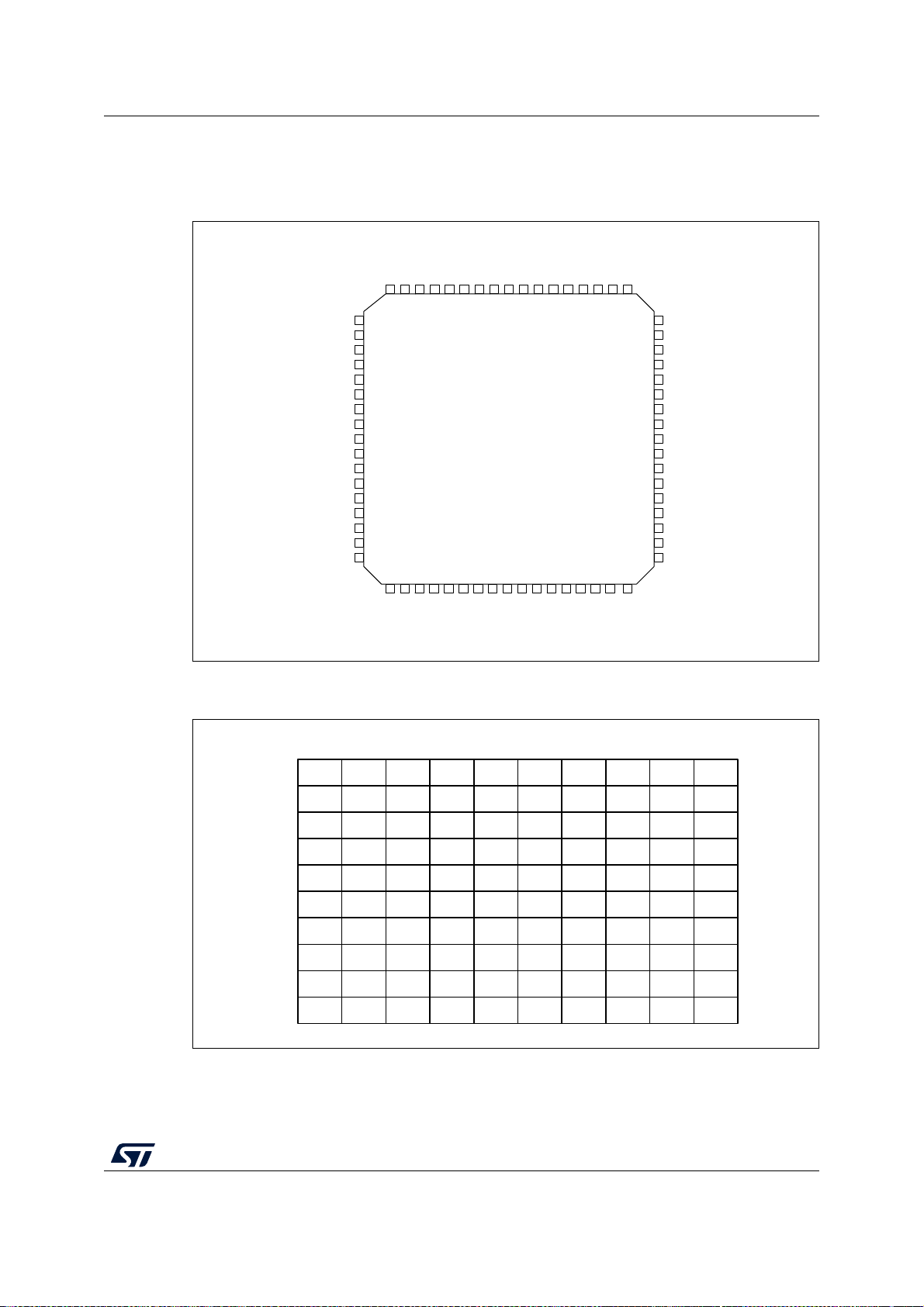
STM32H725xE/G Pinouts, pin descriptions and alternate functions
MSv52556V1.
VFQFPN68
48
46
45
44
43
42
41
40
39
38
37
36
35
47
55
53
52
56
54
61
59
57
646362
60
58
34
VBAT 1
3
4
5
6
7
8
9
10
11
12
13
14
15
16
2
17
26
2829303132
25
27
20
22
24
18
19
21
23
33
49
50
51
VDD
65
66
67
68
PC14-OSC32_IN
PC15-OSC32_OUT
VSSSMPS
VDDSMPS
VSS
PH0-OSC_IN
NRST
PC1
VDDA
VLXSMPS
VFBSMPS
VDD
PH1-OSC_OUT
PC0
VSSA
PA0
VSS
VCAP
PA13
PA11
PA9
PC9
PC6
PB14
PB12
PA12
PA10
PA8
PC7
PB15
PB13
VDD
VDD
VSS
VCAP
PB9
BOOT0
PB6
PB4
PD2
PC11
PA15
PB8
PB7
PB5
PB3
PC12
PC10
PA14
PA1
PA2
PA3
VSS
PA4
PA6
PC4
PB0
PB2
VCAP
VDD
PA5
PA7
PC5
PB1
PB10
VSS
MSv65396V1
PE6 PE5 PE2 PB8 BOOT0 PB5 PD6 PD3 PD2 PC12
12345678910
A
B
C
D
E
F
G
H
J
K
PC14-
OSC32_IN
PC15-
OSC32_OUT
PE3 PE0 PB7 PB3 PD4 PD1 PC11 PC10
VSS VBAT PE4 PE1 PB4 PA15 PA14 PA13
VSSSMPS VLXSMPS PDR_ON PA11
VDDSMPS VFBSMPS PB9 PA10
PC1 NRST
PH0-OSC_IN
PH1-
OSC_OUT
VDDA VSSA PA2 PD13
VREF+ PA1 PA6 PD10
PA4 PA5 PA 7 PB0 PB1 PB12 PB14 PB15
PB6 VSS VDD PD5
PD7 PD0
VCAP PA12
PC13 VDD VDDLDO VSS VDD33USB PA 9
PC0 PC2_C VSS VDD VDD50USB PC6 PC9
PA0 PC3_C PA3 VCAP PD14 PD15 PC7
PA8
PC8
PC4 PE7 PE10 PD11 PD9 PD12
PC5 PB2 PE8 PB11 PB13 PD8
PE9 PB10
5 Pinouts, pin descriptions and alternate functions
Figure 4. VFQFPN68 pinout
1. The above figure shows the package top view.
Figure 5. TFBGA100 pinout
1. The above figure shows the package top view.
DS13311 Rev 2 57/276
113
Pinouts, pin descriptions and alternate functions STM32H725xE/G
MSv52555V1.
LQFP100
10
12
13
14
15
16
17
18
19
20
21
22
23
24
25
9
11
4
6
8
1
2
3
5
7
66
64
63
62
61
60
59
58
57
56
55
54
53
52
51
67
65
72
70
68
75
74
73
71
69
91
89888786858483828180797877
76
92
90
97
95
93
100
99
98
96
94
35
37383940414243444546474849
50
34
36
29
31
33
262728
30
32
PE2
PE4
PE5
VBAT
PC14-OSC32_IN
VSSSMPS
VDDSMPS
PH1-OSC_OUT
PC1
VDD
PC13
PC15-OSC32_OUT
VLXSMPS
PH0-OSC_IN
PC0
PC3_C
VSSA
VDDA
VFBSMPS
NRST
PC2_C
VDD
VREF+
PA0
VSS
VDD
VDDLDO
VSS
PA13
PA11
PA9
PC9
PC6
VDD
VCAP
PA12
PA10
PA8
PC7
PD14
PD13
PD10
PD8
PC8
PD15
VSS
PD12
PD9
PB15
PD11
PA1
PA2
PA3
VDD
PA5
PA7
PC5
PB2
PB10
VSS
PA4
PA6
PC4
PB1
PE8
VCAP
VDD
PB13
PB0
PE7
PB11
VSS
PB12
PB14
VDDLDO
VDD
VDDLDO
VSS
PB9
BOOT0
PB6
PB4
PD5
PD2
VCAP
PB8
PB7
PB5
VDD
PD3
PD0
PC10
PA14
PB3
PD4
PD1
PC12
PA15
VDD33USB
PC11
Figure 6. LQFP100 pinout
1. The above figure shows the package top view.
58/276 DS13311 Rev 2

STM32H725xE/G Pinouts, pin descriptions and alternate functions
MSv52557V1
VSS
VDD
1234567891011
A
B
C
D
E
F
G
H
J
K
L
M
VCAP
VDDLDO
VDD
PA11
PC6
VSS
VDD50USB
VDD33USB
VDD
PD14
VSS
PD15
PD12
PD11
VDD
VSS
VDD
VDDLDO
VSS
N
P
R
T
U
V
W
Y
AA
VDD
PA14
PA12
PA8
PC7
PD13
PD10
PD8
PB15
VCAP
PD3
PD1
PC12
PA15
PA10
PC9
PB13
PB10
PE8
VSS
VSS
PB5
PB4
PB3
PB6
PB7
PA3
PA6
VSS
VDD
VCAP
VDDLDO
PE4
PC13
VBAT
PC0
PC1
VSSA
PA2
PA4
PE2
PC14-
OSC32_IN
VSS
VSSSMPS
VDDSMPS
VSS
PH0-OSC_IN
PH1-
OSC_OUT
VDD
VDDA
PD2
VSS
PC10
PA13
PA9
PC8
PD9
PB14
PB12
PB11
VDD
VDD
VSS
PD5
PD4
PD0
PC11
PE7
PA7
PB0
PB1
PB2
VDD
BOOT0
PB8
PB9
PE0
PDR_ON
PA0
PA1
PA5
PC4
PC5
VSS
VDD
PC15-
OSC32_OUT
VDD
VLXSMPS
VFBSMPS
VDD
NRST
VSS
VREF+
VDD
Figure 7. WLCSP115 ballout
1. The above figure shows the package top view.
DS13311 Rev 2 59/276
113

Pinouts, pin descriptions and alternate functions STM32H725xE/G
MSv52554V1.
LQFP144
23
24
25
26
27
28
29
30
31
32
33
34
35
36
20
22
15
17
19
13
14
16
18
88
86
85
84
83
82
81
80
79
78
77
76
75
74
73
89
87
94
92
90
97
96
95
93
91
135
133
132
131
130
129
128
127
126
125
124
123
122
121
136
134
141
139
137
144
143
142
140
138
47495051525354555657585960
61
72
46
48
41
43
45
383940
42
44
120
119
118
117
116
115
114
113
112
111
110
109
108 PA15
104
107
106
105
103
99
98
101
100
102
686970
71
646566
67
62
63
37
12
11
6
8
10
4
5
7
9
3
2
1PE2
21
VDD
PC13
PC15-OSC32_OUT
VDD
VLXSMPS
VFBSMPS
VDD
PF7
PF9
PH0-OSC_IN
NRST
PC1
PC3_C
VSS
VREF+
PE3
PE5
VBAT
PC14-OSC32_IN
VSS
VSSSMPS
VDDSMPS
VSS
PF6
PF8
PF10
PH1-OSC_OUT
PC0
PC2_C
VDD
VSSA
VDDA
PE4
VSS
PE6
PA13
PA11
PA9
PC9
PC7
VDD
VDD50USB
PG8
PG6
PD14
PD12
VSS
PD10
PD8
PB14
PA14
VDDLDO
PA12
PA10
PA8
PC8
PC6
VDD33USB
VSS
PG7
PD15
PD13
PD11
VDD
PD9
PB15
PB13
VDD
VCAP
VSS
VDD
PE0
PB8
PB7
PB5
PB3
VSS
PG13
PG11
PG9
PD6
VSS
PD4
PD2
PD0
PC11
VDDLDO
VSS
PB9
BOOT0
PB6
PB4
VDD
PG14
PG12
PG10
PD7
VDD
PD5
PD3
PD1
PC12
PC10
PDR_ON
PE1
VCAP
PA0
PA4
PA6
PC4
PB0
PB2
PF14
VSS
PE7
PE9
PE11
PE13
PE15
PB11
VSS
VDD
PA1
PA3
PA5
PA7
PC5
PB1
PF11
PF15
VDD
PE8
PE10
PE12
PE14
PB10
VCAP
VDDLDO
PB12
PA2
VDD
VSS
Figure 8. LQFP144 pinout
1. The above figure shows the package top view.
60/276 DS13311 Rev 2
STM32H725xE/G Pinouts, pin descriptions and alternate functions
MSv52553V1.
LQFP176
8382818079
78
777675
74
73
89
94
92
90
97
96
95
93
91
135
133
132
131
130
129
128
127
126
125
124
123
122
121
136
134
141
139
137
144
143
142
140
138
47495051525354555657585960
61
72
464845
120
119
118
117
116
115
114
113
112
111
110
109
108 PK1
104
107
106
105
103
99
98
101
100
102
686970
71
646566
67
62
63
1PE2
VDD
PC13
PC15-OSC32_OUT
VDD
VLXSMPS
VFBSMPS
PF1
PF3
PF5
VDD
PF7
PF9
PH0-OSC_IN
NRST
PC1
PE3
PE5
VBAT
PC14-OSC32_IN
VSS
VSSSMPS
VDDSMPS
PF0
PF2
PF4
VSS
PF6
PF8
PF10
PH1-OSC_OUT
PC0
PC2_C
PE4
VSS
PE6
PJ9
VSS
PD15
PD13
PD11
VDD
PD9
PB15
PB13
VDD
VDDLDO
VCAP
PB10
PE14
PE12
PK0
VDD
PJ8
VDD
PD14
PD12
VSS
PD10
PD8
PB14
PB12
VSS
VSS
PB11
PE15
PE13
PE11
VSS
PJ10
PJ11
PD1
PA14
VDD
VSS
PA13
PA11
PA9
VDD
PC8
PC6
VDD50USB
PG8
PG6
PG4
VSS
PG2
PD0
PC11
VSS
VDDLDO
VCAP
PA12
PA10
PA8
PC9
PC7
VDD33USB
VSS
PG7
PG5
VDD
PG3
PK2
PC12
PA15
PC10
VSS
VSS
PA4
PA6
PC4
PB0
PB2
PF12
PF14
PG0
VDD
PE7
PE9
VDD
PA3
VDD
PA5
PA7
PC5
PB1
PF11
PF13
PF15
VSS
PG1
PE8
VSS
PE10
PC3_C
PA2
VSSA
VDDA
VDD
VREF+
PA1
PA0
23
24
25
26
27
28
29
30
31
32
33
34
35
36
20
22
15
17
19
13
14
16
18
12
11
6
8
10
4
5
7
9
3
2
21
41
43
38
39
40
42
44
37
8488878685
147
145
148
146
153
151
149
156
155
154
152
150
159
157
160
158
165
163
161
168
167
166
164
162
171
169
172
170
175
173
176
174
PG12
PD7
PD5
PD3
PG11
PG9
PD6
PD4
PD2
PG10
VSS
VDD
PB8
PB3
VDD
PG14
BOOT0
PB6
PG15
VSS
PG13
PB7
PB4
PB5
PDR_ON
VCAP
PE0
VSS
PE1
PB9
VDDLDO
VDD
Figure 9. LQFP176 pinout
1. The above figure shows the package top view.
DS13311 Rev 2 61/276
113
Pinouts, pin descriptions and alternate functions STM32H725xE/G
MSv52551V1.
PE4 PE2 VDD VCAP PB6 VDD VDD PG10 PD5 VDD PC12 PC10
123456789101112
A
B
C
D
E
F
G
H
J
K
L
M
PC15-
OSC32_OUT
PE3 VSS VDDLDO PB8 PB4 VSS PG11 PD6 VSS PC11 PA14
PC14-
OSC32_IN
PE6 PE5 PDR_ON PB9 PG9 PD4 PD1 PA15 VSS
VDD VSS PC13 PD0 PA13 VDDLDO
VLXSMPS VSSSMPS VBAT PA10 PA9 PA8
VDDSMPS VFBSMPS PC9 PC8
VDD VSS PG8 VDD50USB
PH0-OSC_IN
PH1-
OSC_OUT
PF10 PG3 PG5 VSS
PC0 PC1 VSSA PD11 PD13 PD15
PC3_C PC2_C PA1 PA6 PE13 PH10 PH12 PD9 PD10
VDDA VREF+ PA1_C PA 5 PB1 PB2 PG1 PE12 PB10 PH11 PB13 VSS
VDD VSS PH3 VSS PB0 PF11 VSS PE10 PB11 VDDLDO VSS PD8
PE1 PE0 PB7 PG13
PB5 PG14
PD7 PD3
PG12 PD2BOOT0 PG15PF1 PF3
PF0 PC7PG4 PC6PF7 PB3PF2 PF5
PF4 PG7PE7 PG6NRST PF13PF6 PF9
PE8 PG2PA4 PF14PF8
PE9 PE14PA 7 PF15PC3 PA0
PC4 PG0
PH14
13
PH13
VDD
VCAP
PA12
PA11
VDD33USB
VDD
PD14
PD12
VDD
PB15
N
PA2 PH2 PA3 VDD PC5 PF12 VDD PE11 PE15 VCAP VDD PB12 PB14
PA0_C
PC2
MSv52552V1.
VSS PB8 VDDLDO VCAP PB6 PB3 PG11 PG9 PD3 PD1 PA15 PA14
123456789101112
A
B
C
D
E
F
G
H
J
K
L
M
PE4 PE3 PB9 PE0 PB7 PB4 PG13 PD7 PD5 PD2 PC12 PH14
PC13 VSS PE2 PE1 BOOT0 PG10 PD4 PD0 PC11 PC10
PC15-
OSC32_OUT
PC14-
OSC32_IN
PE5 VSS VDD PH15
VSS VBAT PE6 VDD
VLXSMPS VSSSMPS VSS
VDDSMPS VFBSMPS PG8
PF6 PF4 PF5 VSS VDD
PH0-OSC_IN PF8 PF7 VSS PD15
PH1-
OSC_OUT
VSS VDD VSS VSS VSS VSS
NRST PC0 PC1 VREF- VDD
PC2 PC3 VREF+ VDDA PE14
PDR_ON VDD VSS PG15
PB5 PG14
PG12 PD6
VDD
PF1 VSSVSS VSSVSS VSSPF0
PF2 VSSVSS VSSVSS VSSVDD
VSS VSSVSS VSSPF3
VSS VSSVSS VSSPF9
VSS VSS
VDDLDO
13
PA13
PH13
PA9
PC9
VDD33USB
PG7
PG3
PD11
PD9
PD10
PH11
N
PC2_C PC3_C VSSA PH2 PA3 PA 7 PF11 PE8 PG1 PF15 PF13 PB10 PH8
PF10
VCAP
14
PA8
PA10
PC8
PC6
PG6
PG4
PD14
VSS
PB15
PD8
PH9
PH10
VSS
15
PA12
PA11
PC7
VDD50USB
PG5
PG2
PD13
PD12
PB14
PB13
PB12
PH12
P
PA0 PA1 PA1_C PH4 PA4 PA5 PB2 PG0 PE7 PB11 PF12 PE12 PE13 PE15 PH6
R
VSS PA2 PA0_C PH3 PH5 PC4 PA6 PB0 PE10 PF14 PE9 PE11 VCAP VDDLDO VSS
VDD VSS PC5 PB1 VDD VSS PH7
Figure 10. UFBGA169 ballout
1. The above figure shows the package top view.
Figure 11. UFBGA176+25 ballout
1. The above figure shows the package top view.
62/276 DS13311 Rev 2
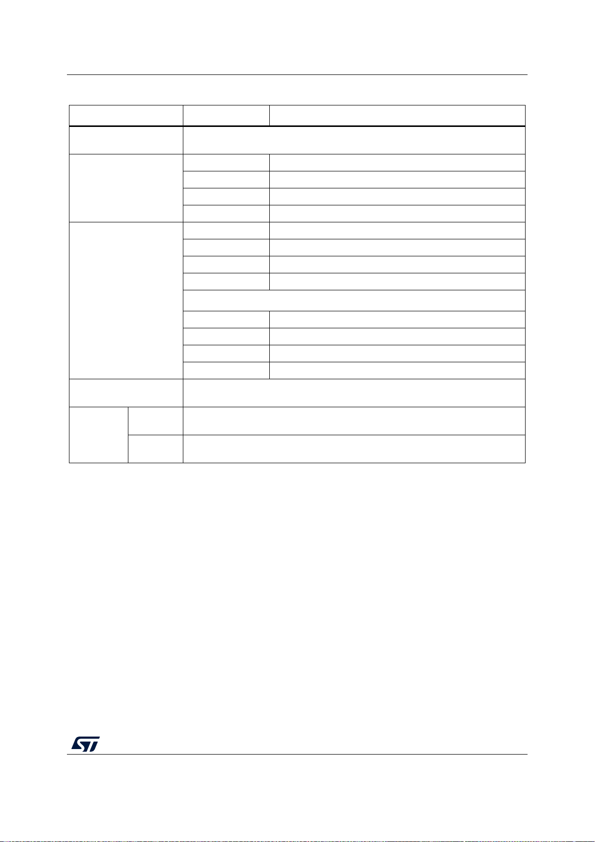
STM32H725xE/G Pinouts, pin descriptions and alternate functions
Table 7. Legend/abbreviations used in the pinout table
Name Abbreviation Definition
Pin name
Unless otherwise specified in brackets below the pin name, the pin function during
and after reset is the same as the actual pin name
S Supply pin
I Input only pin
Pin type
I/O Input / output pin
ANA Analog-only Input
FT 5 V tolerant I/O
TT 3.3 V tolerant I/O
B Dedicated BOOT0 pin
RST Bidirectional reset pin with embedded weak pull-up resistor
I/O structure
Option for TT and FT I/Os
_f I2C FM+ option
_a analog option (supplied by V
_u USB option (supplied by V
)
DDA
DD33USB
)
_h High-speed low-voltage I/O
Notes
Pin functions
Alternate
functions
Additional
functions
Unless otherwise specified by a note, all I/Os are set as floating inputs during and
after reset.
Functions selected through GPIOx_AFR registers
Functions directly selected/enabled through peripheral registers
DS13311 Rev 2 63/276
113

Pinouts, pin descriptions and alternate functions STM32H725xE/G
Table 8. STM32H725 pin and ball descriptions
Pin number
Pin type
I/O structure
LQFP100 SMPS
VFQFPN68 SMPS
TFBGA100 SMPS
LQFP144 SMPS
WLCSP115 SMPS
UFBGA169 SMPS
UFBGA176+25 SMPS
LQFP176 SMPS
Pin name (function after reset)
- 1 A3 1 B11 A2 C3 1 PE2 I/O FT_h -
- - B3 2 - B2 B2 2 PE3 I/O FT_h -
- 2 C3 3 F9 A1 B1 3 PE4 I/O FT_h -
- 3 A2 4 - C3 D3 4 PE5 I/O FT_h -
Notes
Alternate functions
TRACECLK,
SAI1_CK1,
USART10_RX,
SPI4_SCK,
SAI1_MCLK_A,
SAI4_MCLK_A,
OCTOSPIM_P1_IO2,
SAI4_CK1,
ETH_MII_TXD3,
FMC_A23,
EVENTOUT
TRACED0,
TIM15_BKIN,
SAI1_SD_B,
SAI4_SD_B,
USART10_TX,
FMC_A19,
EVENTOUT
TRACED1, SAI1_D2,
DFSDM1_DATIN3,
TIM15_CH1N,
SPI4_NSS,
SAI1_FS_A,
SAI4_FS_A, SAI4_D2,
FMC_A20,
DCMI_D4/PSSI_D4,
LCD_B0, EVENTOUT
TRACED2, SAI1_CK2,
DFSDM1_CKIN3,
TIM15_CH1,
SPI4_MISO,
SAI1_SCK_A,
SAI4_SCK_A,
SAI4_CK2, FMC_A21,
DCMI_D6/PSSI_D6,
LCD_G0, EVENTOUT
Additional functions
-
-
-
-
64/276 DS13311 Rev 2
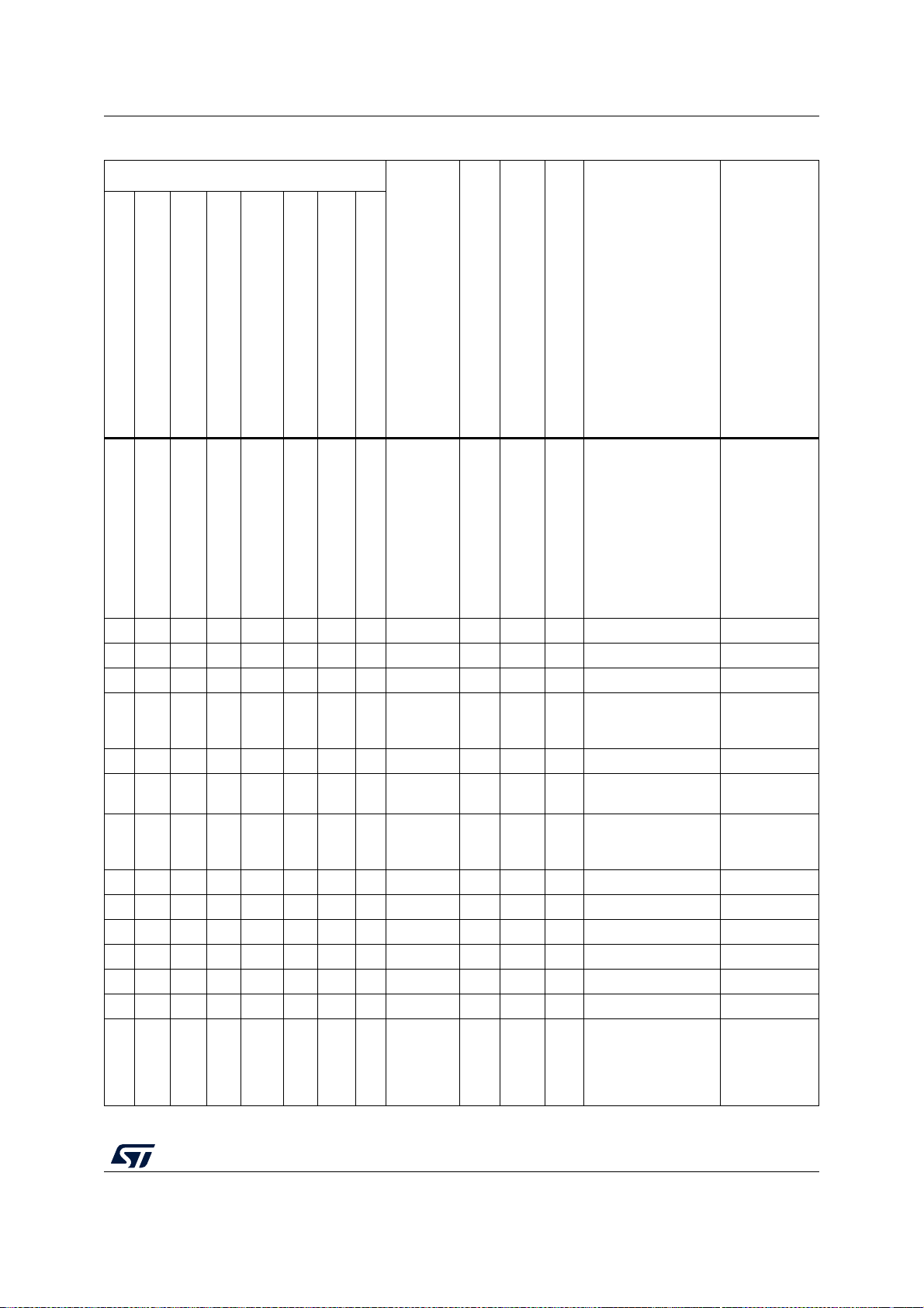
STM32H725xE/G Pinouts, pin descriptions and alternate functions
Table 8. STM32H725 pin and ball descriptions (continued)
Pin number
Pin type
LQFP100 SMPS
VFQFPN68 SMPS
- - A1 5 - C2 E3 5 PE6 I/O FT_h -
- - - 6 - - - 6 VSS S - - - -
-4 - 7 - - -7 VDD S - - - -
1 5 C2 8 K9 E3 E2 8 VBAT S - - - -
- 6 E4 9 H9 D3 C1 9 PC13 I/O FT - EVENTOUT
- - - - F11 - - - VSS S - - - -
27B110D11C1D210
3 8 B2 11 E10 B1 D1 11
- - - 12 F11 - - 12 VSS S - - - -
- - - 13 G10 - - 13 VDD S - - - -
4 9 D1 14 H11 E2 F2 14 VSSSMPS S - - - -
5 10 D2 15 J10 E1 F1 15 VLXSMPS S - - - -
611E116K11F1G116VDDSMPSS - - - -
7 12 E2 17 L10 F2 G2 17 VFBSMPS S - - - -
- - - - - F3 F4 18 PF0 I/O FT_fh -
LQFP144 SMPS
TFBGA100 SMPS
WLCSP115 SMPS
UFBGA169 SMPS
LQFP176 SMPS
UFBGA176+25 SMPS
Pin name (function after reset)
PC14-
OSC32_IN
PC15-
OSC32_
OUT
I/O FT - EVENTOUT OSC32_IN
I/O FT - EVENTOUT OSC32_OUT
Notes
I/O structure
Alternate functions
TRACED3,
TIM1_BKIN2,
SAI1_D1, TIM15_CH2,
SPI4_MOSI,
SAI1_SD_A,
SAI4_SD_A, SAI4_D1,
SAI4_MCLK_B,
TIM1_BKIN2_COMP1
2, FMC_A22,
DCMI_D7/PSSI_D7,
LCD_G1, EVENTOUT
I2C2_SDA(boot),
I2C5_SDA,
OCTOSPIM_P2_IO0,
FMC_A0, TIM23_CH1,
EVENTOUT
Additional functions
-
RTC_TAMP1/
RTC_TS,
WKUP4
-
DS13311 Rev 2 65/276
113

Pinouts, pin descriptions and alternate functions STM32H725xE/G
Table 8. STM32H725 pin and ball descriptions (continued)
Pin number
Pin type
LQFP100 SMPS
VFQFPN68 SMPS
- - - - - E4 F3 19 PF1 I/O FT_fh -
- - - - - F4 G3 20 PF2 I/O FT_h -
- - - - - E5 H4 21 PF3 I/O FT_ha -
- - - - - G3 H2 22 PF4 I/O FT_ha -
- - - - - F5 H3 23 PF5 I/O FT_ha -
8 - - 18 M11 - - 24 VSS S - - - -
9 - - 19 N10 - - 25 VDD S - - - -
- - - 20 - G4 H1 26 PF6 I/O FT_ha -
- - - 21 - F6 J3 27 PF7 I/O FT_ha -
LQFP144 SMPS
TFBGA100 SMPS
WLCSP115 SMPS
UFBGA169 SMPS
LQFP176 SMPS
UFBGA176+25 SMPS
Pin name (function after reset)
Notes
I/O structure
Alternate functions
I2C2_SCL(boot),
I2C5_SCL,
OCTOSPIM_P2_IO1,
FMC_A1, TIM23_CH2,
EVENTOUT
I2C2_SMBA,
I2C5_SMBA,
OCTOSPIM_P2_IO2,
FMC_A2, TIM23_CH3,
EVENTOUT
OCTOSPIM_P2_IO3,
FMC_A3, TIM23_CH4,
EVENTOUT
OCTOSPIM_P2_CLK,
FMC_A4, EVENTOUT
OCTOSPIM_P2_NCL
K, FMC_A5,
EVENTOUT
TIM16_CH1,
FDCAN3_RX,
SPI5_NSS,
SAI1_SD_B,
UART7_RX,
SAI4_SD_B,
OCTOSPIM_P1_IO3,
TIM23_CH1,
EVENTOUT
TIM17_CH1,
FDCAN3_TX,
SPI5_SCK,
SAI1_MCLK_B,
UART7_TX,
SAI4_MCLK_B,
OCTOSPIM_P1_IO2,
TIM23_CH2,
EVENTOUT
ADC3_INP5
ADC3_INN5,
ADC3_INP9
ADC3_INP4
ADC3_INN4,
ADC3_INP8
ADC3_INP3
Additional functions
-
-
66/276 DS13311 Rev 2

STM32H725xE/G Pinouts, pin descriptions and alternate functions
Table 8. STM32H725 pin and ball descriptions (continued)
Pin number
Pin type
LQFP100 SMPS
VFQFPN68 SMPS
- - - 22 - H4 J2 28 PF8 I/O FT_ha -
- - - 23 - G5 J4 29 PF9 I/O FT_ha -
- - - 24 - H3 K3 30 PF10 I/O FT_ha -
10 13 G1 25 P11 H1 J1 31
11 14 G2 26 T11 H2 K1 32
12 15 F2 27 R10 G6 L1 33 NRST I/O RST - - -
13 16 F3 28 M9 J1 L2 34 PC0 I/O FT_ha -
LQFP144 SMPS
TFBGA100 SMPS
WLCSP115 SMPS
UFBGA169 SMPS
LQFP176 SMPS
UFBGA176+25 SMPS
Pin name (function after reset)
PH0-
OSC_IN
PH1-
OSC_OUT
I/O FT - EVENTOUT OSC_IN
I/O FT - EVENTOUT OSC_OUT
Notes
I/O structure
Alternate functions
TIM16_CH1N,
SPI5_MISO,
SAI1_SCK_B,
UART7_RTS/UART7_
DE, SAI4_SCK_B,
TIM13_CH1,
OCTOSPIM_P1_IO0,
TIM23_CH3,
EVENTOUT
TIM17_CH1N,
SPI5_MOSI,
SAI1_FS_B,
UART7_CTS,
SAI4_FS_B,
TIM14_CH1,
OCTOSPIM_P1_IO1,
TIM23_CH4,
EVENTOUT
TIM16_BKIN,
SAI1_D3, PSSI_D15,
OCTOSPIM_P1_CLK,
SAI4_D3,
DCMI_D11/PSSI_D11,
LCD_DE, EVENTOUT
FMC_D12/FMC_AD12
, DFSDM1_CKIN0,
DFSDM1_DATIN4,
SAI4_FS_B,
FMC_A25,
OTG_HS_ULPI_STP,
LCD_G2,
FMC_SDNWE,
LCD_R5, EVENTOUT
ADC3_INN3,
ADC3_INP7
ADC3_INP2
ADC3_INN2,
ADC3_INP6
ADC123_INP10
Additional functions
DS13311 Rev 2 67/276
113

Pinouts, pin descriptions and alternate functions STM32H725xE/G
Table 8. STM32H725 pin and ball descriptions (continued)
Pin number
Pin type
LQFP100 SMPS
VFQFPN68 SMPS
14 17 F1 29 P9 J2 L3 35 PC1 I/O FT_ha -
- - - - - H5 M1 - PC2 I/O FT_a -
- 18 F4 30 - K2 N1 36 PC2_C ANA TT_a - -
- - - - - J4 M2 - PC3 I/O FT_a -
- 19 G4 31 - K1 N2 37 PC3_C ANA TT_a - - ADC3_INP1
- 20 - 32 V11 - - - VDD S - - - -
- 21 - 33 U10 - - - VSS S - - - -
15 22 H2 34 T9 J3 N3 38 VSSA S - - - -
LQFP144 SMPS
TFBGA100 SMPS
WLCSP115 SMPS
UFBGA169 SMPS
LQFP176 SMPS
UFBGA176+25 SMPS
Pin name (function after reset)
Notes
I/O structure
Alternate functions
TRACED0, SAI4_D1,
SAI1_D1,
DFSDM1_DATIN0,
DFSDM1_CKIN4,
SPI2_MOSI/I2S2_SD
O, SAI1_SD_A,
SAI4_SD_A,
SDMMC2_CK,
OCTOSPIM_P1_IO4,
ETH_MDC,
MDIOS_MDC,
LCD_G5, EVENTOUT
PWR_DEEPSLEEP,
DFSDM1_CKIN1,
OCTOSPIM_P1_IO5,
SPI2_MISO/I2S2_SDI,
DFSDM1_CKOUT,
OCTOSPIM_P1_IO2,
OTG_HS_ULPI_DIR,
ETH_MII_TXD2,
FMC_SDNE0,
EVENTOUT
PWR_SLEEP,
DFSDM1_DATIN1,
OCTOSPIM_P1_IO6,
SPI2_MOSI/
I2S2_SDO,
OCTOSPIM_P1_IO0,
OTG_HS_ULPI_NXT,
ETH_MII_TX_CLK,
FMC_SDCKE0,
EVENTOUT
ADC123_INN10
ADC123_INP11
ADC123_INN11
ADC123_INP12
ADC12_INN12,
Additional functions
,
, RTC_TAMP3,
WKUP6
,
ADC3_INN1,
ADC3_INP0
ADC12_INP13
68/276 DS13311 Rev 2

STM32H725xE/G Pinouts, pin descriptions and alternate functions
Table 8. STM32H725 pin and ball descriptions (continued)
Pin number
Pin type
LQFP100 SMPS
VFQFPN68 SMPS
-- - - - -L4- VREF- S - - - -
- 23 J1 35 W10 L2 M3 39 VREF+ S - - - -
16 24 H1 36 Y11 L1 M4 40 VDDA S - - - -
17 25 G3 37 N8 J5 P1 41 PA0 I/O FT_ha -
- - - - - K3 R3 - PA0_C ANA TT_a - -
18 26 J2 38 R8 K4 P2 42 PA1 I/O FT_ha -
- - - - - L3 P3 - PA1_C ANA TT_a - - ADC12_INP1
LQFP144 SMPS
TFBGA100 SMPS
WLCSP115 SMPS
UFBGA169 SMPS
LQFP176 SMPS
UFBGA176+25 SMPS
Pin name (function after reset)
Notes
I/O structure
Alternate functions
TIM2_CH1/TIM2_ETR,
TIM5_CH1,
TIM8_ETR,
TIM15_BKIN,
SPI6_NSS/I2S6_WS,
USART2_CTS/USART
2_NSS, UART4_TX,
SDMMC2_CMD,
SAI4_SD_B,
ETH_MII_CRS,
FMC_A19,
EVENTOUT
TIM2_CH2,
TIM5_CH2,
LPTIM3_OUT,
TIM15_CH1N,
USART2_RTS/USART
2_DE, UART4_RX,
OCTOSPIM_P1_IO3,
SAI4_MCLK_B,
ETH_MII_RX_CLK/ET
H_RMII_REF_CLK,
OCTOSPIM_P1_DQS,
LCD_R2, EVENTOUT
Additional functions
ADC1_INP16,
WKUP1
ADC12_INN1,
ADC12_INP0
ADC1_INN16,
ADC1_INP17
DS13311 Rev 2 69/276
113

Pinouts, pin descriptions and alternate functions STM32H725xE/G
Table 8. STM32H725 pin and ball descriptions (continued)
Pin number
Pin type
LQFP100 SMPS
VFQFPN68 SMPS
19 27 H3 39 V9 N1 R2 43 PA2 I/O FT_ha -
- - - - - N2 N4 - PH2 I/O FT_ha -
- - - - AA10 - - 44 VDD S - - - -
- - - - - - - 45 VSS S - - - -
- - - - - M3 R4 - PH3 I/O FT_ha -
- - - - - - P4 - PH4 I/O FT_fa -
- - - - - - R5 - PH5 I/O
LQFP144 SMPS
TFBGA100 SMPS
WLCSP115 SMPS
UFBGA169 SMPS
LQFP176 SMPS
UFBGA176+25 SMPS
Pin name (function after reset)
FT_fh
a
Notes
I/O structure
Alternate functions
TIM2_CH3,
TIM5_CH3,
LPTIM4_OUT,
TIM15_CH1,
OCTOSPIM_P1_IO0,
USART2_TX(boot),
SAI4_SCK_B,
ETH_MDIO,
MDIOS_MDIO,
LCD_R1, EVENTOUT
LPTIM1_IN2,
OCTOSPIM_P1_IO4,
SAI4_SCK_B,
ETH_MII_CRS,
FMC_SDCKE0,
LCD_R0, EVENTOUT
OCTOSPIM_P1_IO5,
SAI4_MCLK_B,
ETH_MII_COL,
FMC_SDNE0,
LCD_R1, EVENTOUT
I2C2_SCL, LCD_G5,
OTG_HS_ULPI_NXT,
PSSI_D14, LCD_G4,
EVENTOUT
I2C2_SDA,
-
SPI5_NSS,
FMC_SDNWE,
EVENTOUT
ADC12_INP14,
WKUP2
ADC3_INP13
ADC3_INN13,
ADC3_INP14
ADC3_INN14,
ADC3_INP15
ADC3_INN15,
ADC3_INP16
Additional functions
70/276 DS13311 Rev 2

STM32H725xE/G Pinouts, pin descriptions and alternate functions
Table 8. STM32H725 pin and ball descriptions (continued)
Pin number
Pin type
LQFP100 SMPS
VFQFPN68 SMPS
20 28 G5 40 P7 N3 N5 46 PA3 I/O FT_ha -
21 29 - 41 - - - 47 VSS S - - - -
22 30 - 42 - - - 48 VDD S - - - -
23 31 K1 43 Y9 H6 P5 49 PA4 I/O TT_ha -
24 32 K2 44 U8 L4 P6 50 PA5 I/O TT_ha -
LQFP144 SMPS
TFBGA100 SMPS
WLCSP115 SMPS
UFBGA169 SMPS
LQFP176 SMPS
UFBGA176+25 SMPS
Pin name (function after reset)
Notes
I/O structure
Alternate functions
TIM2_CH4,
TIM5_CH4,
LPTIM5_OUT,
TIM15_CH2,
I2S6_MCK,
OCTOSPIM_P1_IO2,
USART2_RX(boot),
LCD_B2,
OTG_HS_ULPI_D0,
ETH_MII_COL,
OCTOSPIM_P1_CLK,
LCD_B5, EVENTOUT
D1PWREN,
TIM5_ETR,
SPI1_NSS(boot)/I2S1
_WS,
SPI3_NSS/I2S3_WS,
USART2_CK,
SPI6_NSS/I2S6_WS,
FMC_D8/FMC_AD8,
DCMI_HSYNC/PSSI_
DE, LCD_VSYNC,
EVENTOUT
D2PWREN,
TIM2_CH1/TIM2_ETR,
TIM8_CH1N,
SPI1_SCK(boot)/I2S1
_CK,
SPI6_SCK/I2S6_CK,
OTG_HS_ULPI_CK,
FMC_D9/FMC_AD9,
PSSI_D14, LCD_R4,
EVENTOUT
ADC12_INP15
ADC12_INP18,
DAC1_OUT1
ADC12_INN18,
ADC12_INP19,
DAC1_OUT2
Additional functions
DS13311 Rev 2 71/276
113

Pinouts, pin descriptions and alternate functions STM32H725xE/G
Table 8. STM32H725 pin and ball descriptions (continued)
Pin number
Pin type
I/O structure
LQFP100 SMPS
VFQFPN68 SMPS
25 33 J3 45 T7 K5 R7 51 PA6 I/O FT_ha -
26 34 K3 46 R6 J6 N6 52 PA7 I/O TT_ha -
27 35 H4 47 W8 K6 R6 53 PC4 I/O TT_ha -
LQFP144 SMPS
TFBGA100 SMPS
WLCSP115 SMPS
UFBGA169 SMPS
LQFP176 SMPS
UFBGA176+25 SMPS
Pin name (function after reset)
Notes
Alternate functions
TIM1_BKIN,
TIM3_CH1,
TIM8_BKIN,
SPI1_MISO(boot)/I2S1
_SDI,
OCTOSPIM_P1_IO3,
SPI6_MISO/I2S6_SDI,
TIM13_CH1,
TIM8_BKIN_COMP12,
MDIOS_MDC,
TIM1_BKIN_COMP12,
DCMI_PIXCLK/PSSI_
PDCK, LCD_G2,
EVENTOUT
TIM1_CH1N,
TIM3_CH2,
TIM8_CH1N,
SPI1_MOSI(boot)/I2S1
_SDO,
SPI6_MOSI/I2S6_SD
O, TIM14_CH1,
OCTOSPIM_P1_IO2,
ETH_MII_RX_DV/ETH
_RMII_CRS_DV,
FMC_SDNWE,
LCD_VSYNC,
EVENTOUT
PWR_DEEPSLEEP,
FMC_A22,
DFSDM1_CKIN2,
I2S1_MCK,
SPDIFRX1_IN3,
SDMMC2_CKIN,
ETH_MII_RXD0/ETH_
RMII_RXD0,
FMC_SDNE0,
LCD_R7, EVENTOUT
Additional functions
ADC12_INP3
ADC12_INN3,
ADC12_INP7,
OPAMP1_VINM
ADC12_INP4,
OPAMP1_
VOUT,
COMP1_INM
72/276 DS13311 Rev 2

STM32H725xE/G Pinouts, pin descriptions and alternate functions
Table 8. STM32H725 pin and ball descriptions (continued)
Pin number
Pin type
LQFP100 SMPS
VFQFPN68 SMPS
28 36 J4 48 AA8 N5 M7 54 PC5 I/O TT_ha -
- - - - V7 - - - VSS S - - - -
-- - -Y7- -- VDD S - - - -
29 37 K4 49 U6 M5 R8 55 PB0 I/O TT_ha -
30 38 K5 50 W6 L5 M8 56 PB1 I/O FT_ha -
LQFP144 SMPS
TFBGA100 SMPS
WLCSP115 SMPS
UFBGA169 SMPS
LQFP176 SMPS
UFBGA176+25 SMPS
Pin name (function after reset)
Notes
I/O structure
Alternate functions
PWR_SLEEP,
SAI4_D3, SAI1_D3,
DFSDM1_DATIN2,
PSSI_D15,
SPDIFRX1_IN4,
OCTOSPIM_P1_DQS,
ETH_MII_RXD1/ETH_
RMII_RXD1,
FMC_SDCKE0,
COMP1_OUT,
LCD_DE, EVENTOUT
TIM1_CH2N,
TIM3_CH3,
TIM8_CH2N,
OCTOSPIM_P1_IO1,
DFSDM1_CKOUT,
UART4_CTS,
LCD_R3,
OTG_HS_ULPI_D1,
ETH_MII_RXD2,
LCD_G1, EVENTOUT
TIM1_CH3N,
TIM3_CH4,
TIM8_CH3N,
OCTOSPIM_P1_IO0,
DFSDM1_DATIN1,
LCD_R6,
OTG_HS_ULPI_D2,
ETH_MII_RXD3,
LCD_G0, EVENTOUT
OPAMP1_VINM
OPAMP1_VINP,
Additional functions
ADC12_INN4,
ADC12_INP8,
ADC12_INN5,
ADC12_INP9,
COMP1_INP
ADC12_INP5,
COMP1_INM
DS13311 Rev 2 73/276
113

Pinouts, pin descriptions and alternate functions STM32H725xE/G
Table 8. STM32H725 pin and ball descriptions (continued)
Pin number
Pin type
LQFP100 SMPS
VFQFPN68 SMPS
31 39 J5 51 AA6 L6 P7 57 PB2 I/O FT_ha -
- - - 52 - M6 N7 58 PF11 I/O FT_ha -
- - - - - N6 P11 59 PF12 I/O FT_ha -
- - - - - G7 N11 60 PF13 I/O FT_ha -
- - - 53 - H7 R10 61 PF14 I/O
- - - 54 - J7 N10 62 PF15 I/O FT_fh -
- - - - - K7 P8 63 PG0 I/O FT_h -
- - - 55 - - - 64 VSS S - - - -
-- -56- - -65 VDD S - - - -
LQFP144 SMPS
TFBGA100 SMPS
WLCSP115 SMPS
UFBGA169 SMPS
LQFP176 SMPS
UFBGA176+25 SMPS
Pin name (function after reset)
FT_fh
a
Notes
I/O structure
RTC_OUT, SAI4_D1,
SAI1_D1,
DFSDM1_CKIN1,
SAI1_SD_A,
SPI3_MOSI/I2S3_SD
O, SAI4_SD_A,
OCTOSPIM_P1_CLK,
OCTOSPIM_P1_DQS,
ETH_TX_ER,
TIM23_ETR,
EVENTOUT
SPI5_MOSI,
OCTOSPIM_P1_NCL
K, SAI4_SD_B,
FMC_NRAS,
DCMI_D12/PSSI_D12,
TIM24_CH1,
EVENTOUT
OCTOSPIM_P2_DQS,
FMC_A6, TIM24_CH2,
EVENTOUT
DFSDM1_DATIN6,
I2C4_SMBA, FMC_A7,
TIM24_CH3,
EVENTOUT
DFSDM1_CKIN6,
I2C4_SCL, FMC_A8,
TIM24_CH4,
EVENTOUT
I2C4_SDA, FMC_A9,
EVENTOUT
OCTOSPIM_P2_IO4,
UART9_RX,
FMC_A10,
EVENTOUT
Alternate functions
Additional functions
COMP1_INP
ADC1_INP2
ADC1_INN2,
ADC1_INP6
ADC2_INP2
ADC2_INN2,
ADC2_INP6
-
-
74/276 DS13311 Rev 2
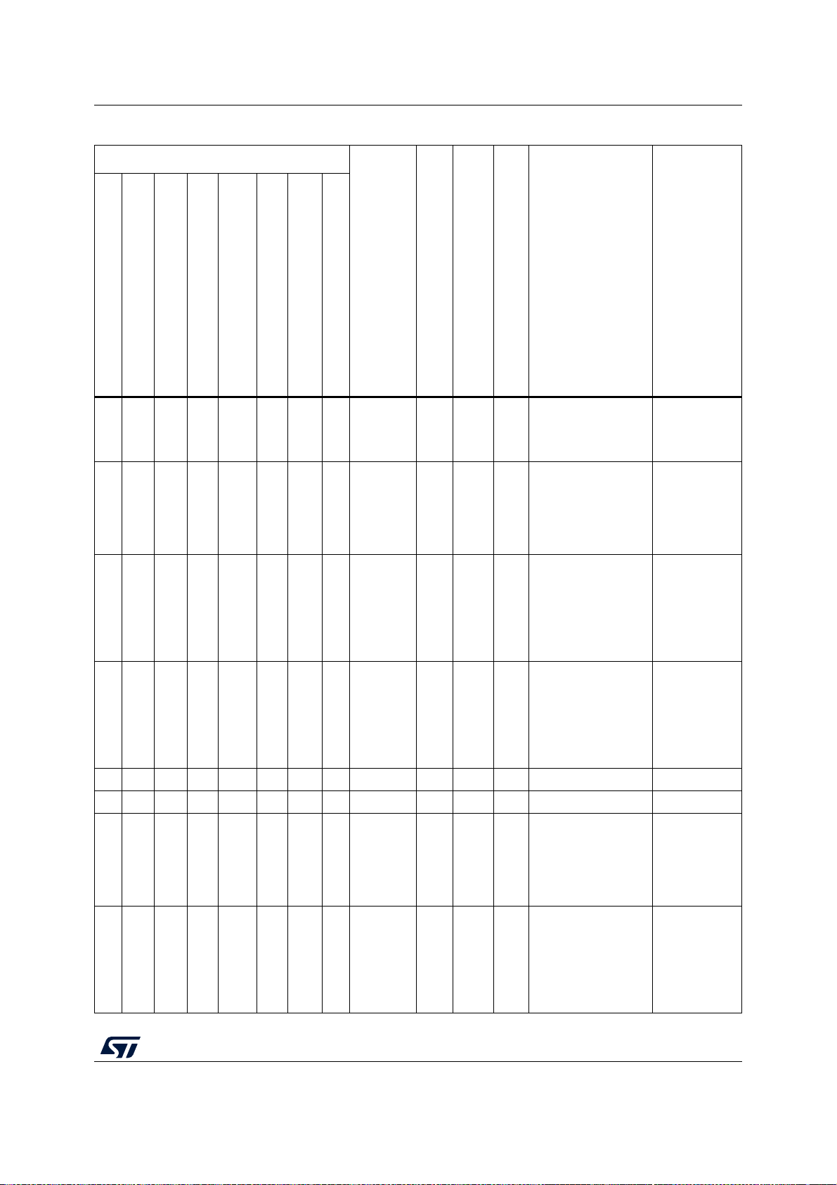
STM32H725xE/G Pinouts, pin descriptions and alternate functions
Table 8. STM32H725 pin and ball descriptions (continued)
Pin number
Pin type
LQFP100 SMPS
VFQFPN68 SMPS
- - - - - L7 N9 66 PG1 I/O TT_h -
- 40 H5 57 N6 G8 P9 67 PE7 I/O TT_ha -
- 41 J6 58 V5 H8 N8 68 PE8 I/O TT_ha -
- - K6 59 - J8 R11 69 PE9 I/O TT_ha -
- - - - Y5 - - 70 VSS S - - - -
-- - -AA4- -71 VDD S - - - -
- - H6 60 - M8 R9 72 PE10 I/O FT_ha -
- - - 61 - N8 R12 73 PE11 I/O FT_ha -
LQFP144 SMPS
TFBGA100 SMPS
WLCSP115 SMPS
UFBGA169 SMPS
LQFP176 SMPS
UFBGA176+25 SMPS
Pin name (function after reset)
Notes
I/O structure
Alternate functions
OCTOSPIM_P2_IO5,
UART9_TX,
FMC_A11,
EVENTOUT
TIM1_ETR,
DFSDM1_DATIN2,
UART7_RX,
OCTOSPIM_P1_IO4,
FMC_D4/FMC_AD4,
EVENTOUT
TIM1_CH1N,
DFSDM1_CKIN2,
UART7_TX,
OCTOSPIM_P1_IO5,
FMC_D5/FMC_AD5,
COMP2_OUT,
EVENTOUT
TIM1_CH1,
DFSDM1_CKOUT,
UART7_RTS/UART7_
DE,
OCTOSPIM_P1_IO6,
FMC_D6/FMC_AD6,
EVENTOUT
TIM1_CH2N,
DFSDM1_DATIN4,
UART7_CTS,
OCTOSPIM_P1_IO7,
FMC_D7/FMC_AD7,
EVENTOUT
TIM1_CH2,
DFSDM1_CKIN4,
SPI4_NSS(boot),
SAI4_SD_B,
OCTOSPIM_P1_NCS,
FMC_D8/FMC_AD8,
LCD_G3, EVENTOUT
OPAMP2_VINM
OPAMP2_VINM
OPAMP2_VINP,
Additional functions
OPAMP2_
VOUT,
COMP2_INM
COMP2_INP
COMP2_INM
COMP2_INP
DS13311 Rev 2 75/276
113

Pinouts, pin descriptions and alternate functions STM32H725xE/G
Table 8. STM32H725 pin and ball descriptions (continued)
Pin number
Pin type
I/O structure
LQFP100 SMPS
VFQFPN68 SMPS
- - - 62 - L8 P12 74 PE12 I/O FT_h -
- - - 63 - K8 P13 75 PE13 I/O FT_h -
- - - 64 - J9 M12 76 PE14 I/O FT_h -
- - - 65 - N9 P14 77 PE15 I/O FT_h -
32 42 K7 66 T5 L9 N12 78 PB10 I/O FT_fh -
LQFP144 SMPS
TFBGA100 SMPS
WLCSP115 SMPS
UFBGA169 SMPS
LQFP176 SMPS
UFBGA176+25 SMPS
Pin name (function after reset)
Notes
Alternate functions
TIM1_CH3N,
DFSDM1_DATIN5,
SPI4_SCK(boot),
SAI4_SCK_B,
FMC_D9/FMC_AD9,
COMP1_OUT,
LCD_B4, EVENTOUT
TIM1_CH3,
DFSDM1_CKIN5,
SPI4_MISO(boot),
SAI4_FS_B,
FMC_D10/FMC_AD10
, COMP2_OUT,
LCD_DE, EVENTOUT
TIM1_CH4,
SPI4_MOSI(boot),
SAI4_MCLK_B,
FMC_D11/FMC_AD11,
LCD_CLK,
EVENTOUT
TIM1_BKIN,
USART10_CK,
FMC_D12/FMC_AD12
,
TIM1_BKIN_COMP12,
LCD_R7, EVENTOUT
TIM2_CH3,
LPTIM2_IN1,
I2C2_SCL,
SPI2_SCK/I2S2_CK,
DFSDM1_DATIN7,
USART3_TX(boot),
OCTOSPIM_P1_NCS,
OTG_HS_ULPI_D3,
ETH_MII_RX_ER,
LCD_G4, EVENTOUT
Additional functions
-
-
-
-
-
76/276 DS13311 Rev 2
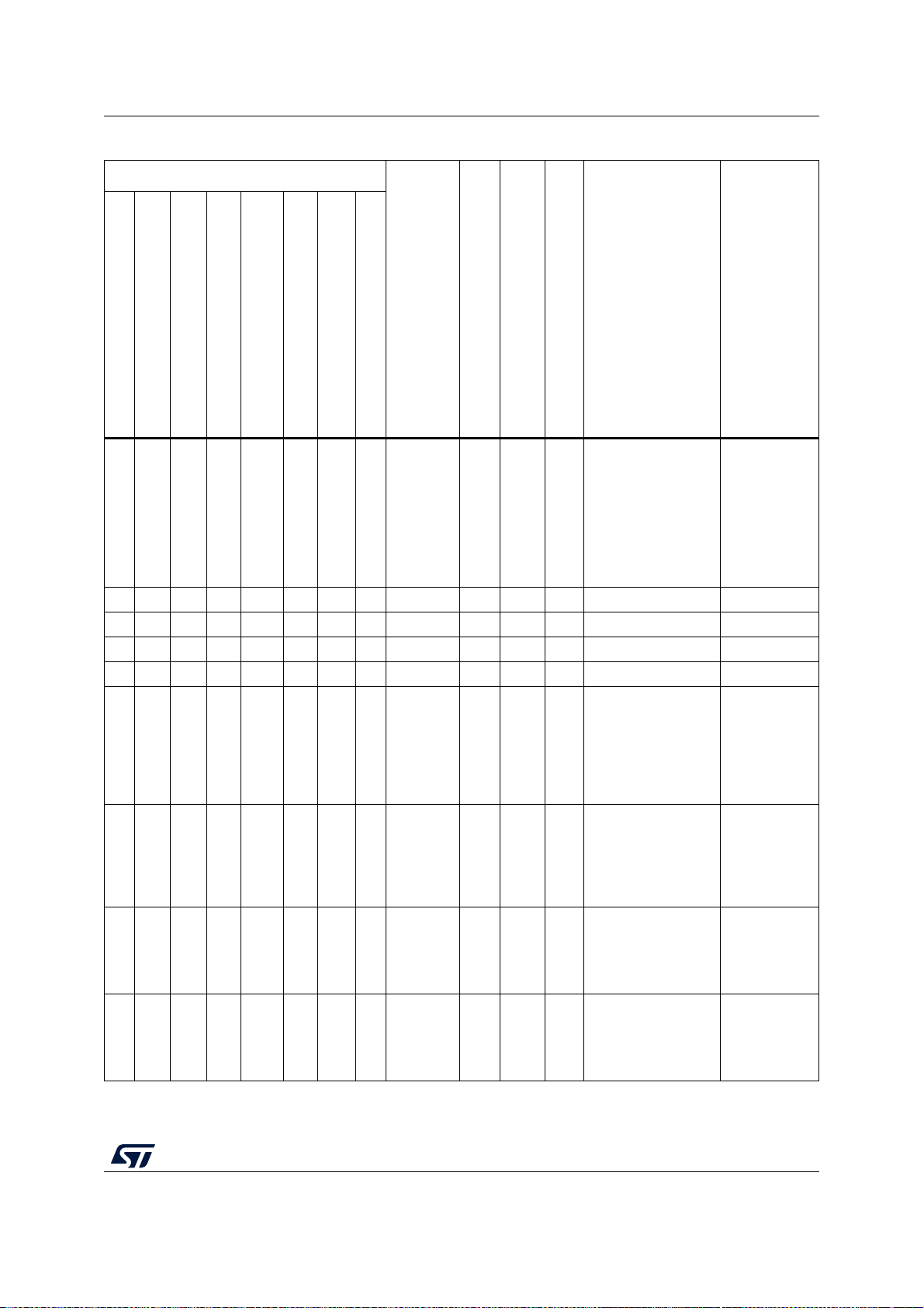
STM32H725xE/G Pinouts, pin descriptions and alternate functions
Table 8. STM32H725 pin and ball descriptions (continued)
Pin number
Pin type
LQFP100 SMPS
VFQFPN68 SMPS
- 43 J7 67 W4 M9 P10 79 PB11 I/O FT_f -
33 44 G6 68 Y3 N10 R13 80 VCAP S - - - -
34 45 - 69 AA2 - - 81 VSS S - - - -
- 46 F7 70 W2 M10 R14 82 VDDLDO S - - - -
35 47 - 71 Y1 - - - VDD S - - - -
- - - - - - P15 - PH6 I/O FT_h -
- - - - - - M11 - PH7 I/O FT_fh -
- - - - - - N13 - PH8 I/O FT_fh -
- - - - - - M14 - PH9 I/O FT_h -
LQFP144 SMPS
TFBGA100 SMPS
WLCSP115 SMPS
UFBGA169 SMPS
LQFP176 SMPS
UFBGA176+25 SMPS
Pin name (function after reset)
Notes
I/O structure
Alternate functions
TIM2_CH4,
LPTIM2_ETR,
I2C2_SDA,
DFSDM1_CKIN7,
USART3_RX(boot),
OTG_HS_ULPI_D4,
ETH_MII_TX_EN/ETH
_RMII_TX_EN,
LCD_G5, EVENTOUT
TIM12_CH1,
I2C2_SMBA,
SPI5_SCK,
ETH_MII_RXD2,
FMC_SDNE1,
DCMI_D8/PSSI_D8,
EVENTOUT
I2C3_SCL,
SPI5_MISO,
ETH_MII_RXD3,
FMC_SDCKE1,
DCMI_D9/PSSI_D9,
EVENTOUT
TIM5_ETR,
I2C3_SDA, FMC_D16,
DCMI_HSYNC/PSSI_
DE, LCD_R2,
EVENTOUT
TIM12_CH2,
I2C3_SMBA,
FMC_D17,
DCMI_D0/PSSI_D0,
LCD_R3, EVENTOUT
Additional functions
-
-
-
-
-
DS13311 Rev 2 77/276
113
Pinouts, pin descriptions and alternate functions STM32H725xE/G
Table 8. STM32H725 pin and ball descriptions (continued)
Pin number
Pin type
LQFP100 SMPS
VFQFPN68 SMPS
- - - - - K9 N14 - PH10 I/O FT_h -
- - - - - L10 M13 - PH11 I/O FT_fh -
- - - - - - - 83 VSS S - - - -
- - - - Y1 - - 84 VDD S - - - -
- - - - - K10 N15 - PH12 I/O FT_fh -
36 48 K8 72 U4 N12 M15 85 PB12 I/O FT_h -
LQFP144 SMPS
TFBGA100 SMPS
WLCSP115 SMPS
UFBGA169 SMPS
LQFP176 SMPS
UFBGA176+25 SMPS
Pin name (function after reset)
Notes
I/O structure
Alternate functions
TIM5_CH1,
I2C4_SMBA,
FMC_D18,
DCMI_D1/PSSI_D1,
LCD_R4, EVENTOUT
TIM5_CH2, I2C4_SCL,
FMC_D19,
DCMI_D2/PSSI_D2,
LCD_R5, EVENTOUT
TIM5_CH3,
I2C4_SDA, FMC_D20,
DCMI_D3/PSSI_D3,
LCD_R6, EVENTOUT
TIM1_BKIN,
OCTOSPIM_P1_NCL
K, I2C2_SMBA,
SPI2_NSS/I2S2_WS,
DFSDM1_DATIN1,
USART3_CK,
FDCAN2_RX,
OTG_HS_ULPI_D5,
ETH_MII_TXD0/ETH_
RMII_TXD0,
OCTOSPIM_P1_IO0,
TIM1_BKIN_COMP12,
UART5_RX,
EVENTOUT
Additional functions
-
-
-
-
78/276 DS13311 Rev 2
STM32H725xE/G Pinouts, pin descriptions and alternate functions
Table 8. STM32H725 pin and ball descriptions (continued)
Pin number
Pin type
I/O structure
LQFP100 SMPS
VFQFPN68 SMPS
37 49 J8 73 P5 L11 L15 86 PB13 I/O FT_h -
38 50 K9 74 R4 N13 K15 87 PB14 I/O FT_h -
39 51 K10 75 V3 M13 K14 88 PB15 I/O FT_h -
LQFP144 SMPS
TFBGA100 SMPS
WLCSP115 SMPS
UFBGA169 SMPS
LQFP176 SMPS
UFBGA176+25 SMPS
Pin name (function after reset)
Notes
Alternate functions
TIM1_CH1N,
LPTIM2_OUT,
OCTOSPIM_P1_IO2,
SPI2_SCK/I2S2_CK,
DFSDM1_CKIN1,
USART3_CTS/USART
3_NSS, FDCAN2_TX,
OTG_HS_ULPI_D6,
ETH_MII_TXD1/ETH_
RMII_TXD1,
SDMMC1_D0,
DCMI_D2/PSSI_D2,
UART5_TX,
EVENTOUT
TIM1_CH2N,
TIM12_CH1,
TIM8_CH2N,
USART1_TX,
SPI2_MISO/I2S2_SDI,
DFSDM1_DATIN2,
USART3_RTS/USART
3_DE,
UART4_RTS/UART4_
DE, SDMMC2_D0,
FMC_D10/FMC_AD10
, LCD_CLK,
EVENTOUT
RTC_REFIN,
TIM1_CH3N,
TIM12_CH2,
TIM8_CH3N,
USART1_RX,
SPI2_MOSI/I2S2_SD
O, DFSDM1_CKIN2,
UART4_CTS,
SDMMC2_D1,
FMC_D11/FMC_AD11,
LCD_G7, EVENTOUT
Additional functions
-
-
-
DS13311 Rev 2 79/276
113

Pinouts, pin descriptions and alternate functions STM32H725xE/G
Table 8. STM32H725 pin and ball descriptions (continued)
Pin number
Pin type
LQFP100 SMPS
VFQFPN68 SMPS
- 52 J9 76 T3 M12 L14 89 PD8 I/O FT_h -
- 53 H8 77 N4 K11 K13 90 PD9 I/O FT_h -
- 54 J10 78 P3 K12 L13 91 PD10 I/O FT_h -
-- -79V1- -92 VDD S - - - -
- - - 80 U2 - - 93 VSS S - - - -
- 55 H7 81 R2 J10 J13 94 PD11 I/O FT_h -
- 56 H9 82 T1 K13 J15 95 PD12 I/O FT_fh -
LQFP144 SMPS
TFBGA100 SMPS
WLCSP115 SMPS
UFBGA169 SMPS
LQFP176 SMPS
UFBGA176+25 SMPS
Pin name (function after reset)
Notes
I/O structure
Alternate functions
DFSDM1_CKIN3,
USART3_TX(boot),
SPDIFRX1_IN2,
FMC_D13/FMC_AD13
, EVENTOUT
DFSDM1_DATIN3,
USART3_RX(boot),
FMC_D14/FMC_AD14
, EVENTOUT
DFSDM1_CKOUT,
USART3_CK,
FMC_D15/FMC_AD15
, LCD_B3, EVENTOUT
LPTIM2_IN2,
I2C4_SMBA,
USART3_CTS/USART
3_NSS,
OCTOSPIM_P1_IO0,
SAI4_SD_A,
FMC_A16/FMC_CLE,
EVENTOUT
LPTIM1_IN1,
TIM4_CH1,
LPTIM2_IN1,
I2C4_SCL,
FDCAN3_RX,
USART3_RTS/USART
3_DE,
OCTOSPIM_P1_IO1,
SAI4_FS_A,
FMC_A17/FMC_ALE,
DCMI_D12/PSSI_D12,
EVENTOUT
Additional functions
-
-
-
-
-
80/276 DS13311 Rev 2

STM32H725xE/G Pinouts, pin descriptions and alternate functions
Table 8. STM32H725 pin and ball descriptions (continued)
Pin number
Pin type
LQFP100 SMPS
VFQFPN68 SMPS
- 57 H10 83 M3 J11 H15 96 PD13 I/O FT_fh -
- 58 - - - - - - VSS S - - - -
-59 - - - - - - VDD S - - - -
- 60 G7 84 L2 J13 H14 97 PD14 I/O FT_h -
- 61 G8 85 N2 J12 J12 98 PD15 I/O FT_h -
-- - - - - -99 VDD S - - - -
- - - - P1 - - 100 VSS S - - - -
- - - - - - - 101 PJ8 I/O FT -
- - - - - - - 102 PJ9 I/O FT -
- - - - - - - 103 PJ10 I/O FT -
LQFP144 SMPS
TFBGA100 SMPS
WLCSP115 SMPS
UFBGA169 SMPS
LQFP176 SMPS
UFBGA176+25 SMPS
Pin name (function after reset)
Notes
I/O structure
Alternate functions
LPTIM1_OUT,
TIM4_CH2,
I2C4_SDA,
FDCAN3_TX,
OCTOSPIM_P1_IO3,
SAI4_SCK_A,
UART9_RTS/UART9_
DE, FMC_A18,
DCMI_D13/PSSI_D13,
EVENTOUT
TIM4_CH3,
UART8_CTS,
UART9_RX,
FMC_D0/FMC_AD0,
EVENTOUT
TIM4_CH4,
UART8_RTS/UART8_
DE, UART9_TX,
FMC_D1/FMC_AD1,
EVENTOUT
TIM1_CH3N,
TIM8_CH1,
UART8_TX, LCD_G1,
EVENTOUT
TIM1_CH3,
TIM8_CH1N,
UART8_RX, LCD_G2,
EVENTOUT
TIM1_CH2N,
TIM8_CH2,
SPI5_MOSI, LCD_G3,
EVENTOUT
Additional functions
-
-
-
-
-
-
DS13311 Rev 2 81/276
113

Pinouts, pin descriptions and alternate functions STM32H725xE/G
Table 8. STM32H725 pin and ball descriptions (continued)
Pin number
Pin type
LQFP100 SMPS
VFQFPN68 SMPS
- - - - - - - 104 PJ11 I/O FT -
- - - - M1 - - 105 VDD S - - - -
- - - - - - - 106 VSS S - - - -
- - - - - - - 107 PK0 I/O FT -
- - - - - - - 108 PK1 I/O FT -
- - - - - - - 109 PK2 I/O FT -
- - - - - H9 G15 110 PG2 I/O FT_h -
- - - - - H10 H13 111 PG3 I/O FT_h -
- - - - - - - 112 VSS S - - - -
-- - -M1- -113VDD S - - - -
- - - - - F8 G14 114 PG4 I/O FT_h -
LQFP144 SMPS
TFBGA100 SMPS
WLCSP115 SMPS
UFBGA169 SMPS
LQFP176 SMPS
UFBGA176+25 SMPS
Pin name (function after reset)
Notes
I/O structure
Alternate functions
TIM1_CH2,
TIM8_CH2N,
SPI5_MISO, LCD_G4,
EVENTOUT
TIM1_CH1N,
TIM8_CH3,
SPI5_SCK, LCD_G5,
EVENTOUT
TIM1_CH1,
TIM8_CH3N,
SPI5_NSS, LCD_G6,
EVENTOUT
TIM1_BKIN,
TIM8_BKIN,
TIM8_BKIN_COMP12,
TIM1_BKIN_COMP12,
LCD_G7, EVENTOUT
TIM8_BKIN,
TIM8_BKIN_COMP12,
FMC_A12,
TIM24_ETR,
EVENTOUT
TIM8_BKIN2,
TIM8_BKIN2_COMP1
2, FMC_A13,
TIM23_ETR,
EVENTOUT
TIM1_BKIN2,
TIM1_BKIN2_COMP1
2,
FMC_A14/FMC_BA0,
EVENTOUT
Additional functions
-
-
-
-
-
-
-
82/276 DS13311 Rev 2

STM32H725xE/G Pinouts, pin descriptions and alternate functions
Table 8. STM32H725 pin and ball descriptions (continued)
Pin number
Pin type
LQFP100 SMPS
VFQFPN68 SMPS
- - - - - H11 F15 115 PG5 I/O FT_h -
- - - 86 - G9 F14 116 PG6 I/O FT_h -
- - - 87 - G10 G13 117 PG7 I/O FT_h -
- - - 88 - G11 G12 118 PG8 I/O FT_h -
- - - 89 P1 - - 119 VSS S - - - -
- - - 90 K1 G12 E15 120
- - E8 91 J2 G13 F13 121
-- -92- - - - VDD S - - - -
LQFP144 SMPS
TFBGA100 SMPS
WLCSP115 SMPS
UFBGA169 SMPS
LQFP176 SMPS
UFBGA176+25 SMPS
Pin name (function after reset)
VDD50US
B
VDD33US
B
S-- - -
S-- - -
Notes
I/O structure
Alternate functions
TIM1_ETR,
FMC_A15/FMC_BA1,
EVENTOUT
TIM17_BKIN,
OCTOSPIM_P1_NCS,
FMC_NE3,
DCMI_D12/PSSI_D12,
LCD_R7, EVENTOUT
SAI1_MCLK_A,
USART6_CK,
OCTOSPIM_P2_DQS,
FMC_INT,
DCMI_D13/PSSI_D13,
LCD_CLK,
EVENTOUT
TIM8_ETR,
SPI6_NSS/I2S6_WS,
USART6_RTS/USART
6_DE,
SPDIFRX1_IN3,
ETH_PPS_OUT,
FMC_SDCLK,
LCD_G7, EVENTOUT
Additional functions
-
-
-
-
DS13311 Rev 2 83/276
113

Pinouts, pin descriptions and alternate functions STM32H725xE/G
Table 8. STM32H725 pin and ball descriptions (continued)
Pin number
Pin type
I/O structure
LQFP100 SMPS
VFQFPN68 SMPS
40 62 F8 93 H1 F9 E14 122 PC6 I/O FT_h -
41 63 G9 94 K3 F10 D15 123 PC7 I/O FT_h -
- 64 G10 95 L4 F12 D14 124 PC8 I/O FT_h -
LQFP144 SMPS
TFBGA100 SMPS
WLCSP115 SMPS
UFBGA169 SMPS
LQFP176 SMPS
UFBGA176+25 SMPS
Pin name (function after reset)
Notes
Alternate functions
TIM3_CH1,
TIM8_CH1,
DFSDM1_CKIN3,
I2S2_MCK,
USART6_TX,
SDMMC1_D0DIR,
FMC_NWAIT,
SDMMC2_D6,
SDMMC1_D6,
DCMI_D0/PSSI_D0,
LCD_HSYNC,
EVENTOUT
DBTRGIO, TIM3_CH2,
TIM8_CH2,
DFSDM1_DATIN3,
I2S3_MCK,
USART6_RX,
SDMMC1_D123DIR,
FMC_NE1,
SDMMC2_D7,
SWPMI_TX,
SDMMC1_D7,
DCMI_D1/PSSI_D1,
LCD_G6, EVENTOUT
TRACED1,
TIM3_CH3,
TIM8_CH3,
USART6_CK,
UART5_RTS/UART5_
DE,
FMC_NE2/FMC_NCE,
FMC_INT,
SWPMI_RX,
SDMMC1_D0,
DCMI_D2/PSSI_D2,
EVENTOUT
Additional functions
SWPMI_IO
-
-
84/276 DS13311 Rev 2
STM32H725xE/G Pinouts, pin descriptions and alternate functions
Table 8. STM32H725 pin and ball descriptions (continued)
Pin number
Pin type
LQFP100 SMPS
VFQFPN68 SMPS
42 65 F9 96 M5 F11 E13 125 PC9 I/O FT_fh -
- - - - G2 - - - VSS S - - - -
- - - - F1 - - 126 VDD S - - - -
43 66 F10 97 H3 E12 B14 127 PA8 I/O FT_fh -
44 67 E9 98 J4 E11 D13 128 PA9 I/O FT_u -
45 68 E10 99 K5 E10 C14 129 PA10 I/O FT_u -
LQFP144 SMPS
TFBGA100 SMPS
WLCSP115 SMPS
UFBGA169 SMPS
LQFP176 SMPS
UFBGA176+25 SMPS
Pin name (function after reset)
Notes
I/O structure
Alternate functions
MCO2, TIM3_CH4,
TIM8_CH4,
I2C3_SDA(boot),
I2S_CKIN, I2C5_SDA,
UART5_CTS,
OCTOSPIM_P1_IO0,
LCD_G3,
SWPMI_SUSPEND,
SDMMC1_D1,
DCMI_D3/PSSI_D3,
LCD_B2, EVENTOUT
MCO1, TIM1_CH1,
TIM8_BKIN2,
I2C3_SCL(boot),
I2C5_SCL,
USART1_CK,
OTG_HS_SOF,
UART7_RX,
TIM8_BKIN2_COMP1
2, LCD_B3, LCD_R6,
EVENTOUT
TIM1_CH2,
LPUART1_TX,
I2C3_SMBA,
SPI2_SCK/I2S2_CK,
I2C5_SMBA,
USART1_TX(boot),
ETH_TX_ER,
DCMI_D0/PSSI_D0,
LCD_R5, EVENTOUT
TIM1_CH3,
LPUART1_RX,
USART1_RX(boot),
OTG_HS_ID,
MDIOS_MDIO,
LCD_B4,
DCMI_D1/PSSI_D1,
LCD_B1, EVENTOUT
OTG_HS_
Additional functions
-
-
VBUS
-
DS13311 Rev 2 85/276
113

Pinouts, pin descriptions and alternate functions STM32H725xE/G
Table 8. STM32H725 pin and ball descriptions (continued)
Pin number
Pin type
LQFP100 SMPS
VFQFPN68 SMPS
46 69 D10 100 E2 F13 C15 130 PA11 I/O FT_u -
47 70 D9 101 F3 E13 B15 131 PA12 I/O FT_u -
48 71 C10 102 G4 D11 B13 132
49 72 D8 103 D1 D13 A14 133 VCAP S - - - -
50 73 - 104 B1 - - 134 VSS S - - - -
- 74 E6 105 C2 D12 A13 135 VDDLDO S - - - -
51 75 - 106 A2 - - 136 VDD S - - - -
-76 - - - - - -
- - - - - B13 C13 - PH13 I/O FT_h -
- - - - - A13 B12 - PH14 I/O FT_h -
LQFP144 SMPS
TFBGA100 SMPS
WLCSP115 SMPS
UFBGA169 SMPS
LQFP176 SMPS
UFBGA176+25 SMPS
Pin name (function after reset)
PA13(JTM
S/
SWDIO)
VDD33US
B
I/O FT -
S-- - -
Notes
I/O structure
Alternate functions
TIM1_CH4,
LPUART1_CTS,
SPI2_NSS/I2S2_WS,
UART4_RX,
USART1_CTS/USART
1_NSS, FDCAN1_RX,
LCD_R4, EVENTOUT
TIM1_ETR,
LPUART1_RTS/LPUA
RT1_DE,
SPI2_SCK/I2S2_CK,
UART4_TX,
USART1_RTS/USART
1_DE, SAI4_FS_B,
FDCAN1_TX,
TIM1_BKIN2,
LCD_R5, EVENTOUT
JTMS/SWDIO,
EVENTOUT
TIM8_CH1N,
UART4_TX,
FDCAN1_TX(boot),
FMC_D21, LCD_G2,
EVENTOUT
TIM8_CH2N,
UART4_RX,
FDCAN1_RX(boot),
FMC_D22,
DCMI_D4/PSSI_D4,
LCD_G3, EVENTOUT
OTG_HS_DM
(boot)
OTG_HS_DP
(boot)
Additional functions
-
-
-
86/276 DS13311 Rev 2

STM32H725xE/G Pinouts, pin descriptions and alternate functions
Table 8. STM32H725 pin and ball descriptions (continued)
Pin number
Pin type
LQFP100 SMPS
VFQFPN68 SMPS
- - - - - - D12 - PH15 I/O FT_h -
- - - - - - - 137 VSS S - - - -
-- - -A2- -- VDD S - - - -
52 77 C9 107 D3 B12 A12 138
53 78 C8 108 H5 C11 A11 139 PA15(JTDI) I/O FT -
54 79 B10 109 E4 A12 C12 140 PC10 I/O FT_fh -
55 80 B9 110 L6 B11 C11 141 PC11 I/O FT_fh -
LQFP144 SMPS
TFBGA100 SMPS
WLCSP115 SMPS
UFBGA169 SMPS
LQFP176 SMPS
UFBGA176+25 SMPS
Pin name (function after reset)
PA14(JTC
K/SWCLK)
I/O FT -
Notes
I/O structure
Alternate functions
TIM8_CH3N,
FMC_D23,
DCMI_D11/PSSI_D11,
LCD_G4, EVENTOUT
JTCK/SWCLK,
EVENTOUT
JTDI,
TIM2_CH1/TIM2_ETR,
CEC,
SPI1_NSS/I2S1_WS,
SPI3_NSS/I2S3_WS,
SPI6_NSS/I2S6_WS,
UART4_RTS/UART4_
DE, LCD_R3,
UART7_TX, LCD_B6,
EVENTOUT
DFSDM1_CKIN5,
I2C5_SDA,
SPI3_SCK(boot)/I2S3
_CK, USART3_TX,
UART4_TX,
OCTOSPIM_P1_IO1,
LCD_B1, SWPMI_RX,
SDMMC1_D2,
DCMI_D8/PSSI_D8,
LCD_R2, EVENTOUT
DFSDM1_DATIN5,
I2C5_SCL,
SPI3_MISO(boot)/I2S3
_SDI, USART3_RX,
UART4_RX,
OCTOSPIM_P1_NCS,
SDMMC1_D3,
DCMI_D4/PSSI_D4,
LCD_B4, EVENTOUT
Additional functions
-
-
-
-
-
DS13311 Rev 2 87/276
113

Pinouts, pin descriptions and alternate functions STM32H725xE/G
Table 8. STM32H725 pin and ball descriptions (continued)
Pin number
Pin type
LQFP100 SMPS
VFQFPN68 SMPS
56 81 A10 111 F5 A11 B11 142 PC12 I/O FT_h -
-- - -B3- -- VDD S - - - -
- - - - C4 - - - VSS S - - - -
- 82 C7 112 J6 D10 C10 143 PD0 I/O FT_h -
- 83 B8 113 D5 C10 A10 144 PD1 I/O FT_h -
57 84 A9 114 A4 E9 B10 145 PD2 I/O FT_h -
- 85 A8 115 B5 D9 A9 146 PD3 I/O FT_h -
LQFP144 SMPS
TFBGA100 SMPS
WLCSP115 SMPS
UFBGA169 SMPS
LQFP176 SMPS
UFBGA176+25 SMPS
Pin name (function after reset)
Notes
I/O structure
Alternate functions
TRACED3,
FMC_D6/FMC_AD6,
TIM15_CH1,
I2C5_SMBA,
SPI6_SCK/I2S6_CK,
SPI3_MOSI(boot)/I2S3
_SDO, USART3_CK,
UART5_TX,
SDMMC1_CK,
DCMI_D9/PSSI_D9,
LCD_R6, EVENTOUT
DFSDM1_CKIN6,
UART4_RX,
FDCAN1_RX(boot),
UART9_CTS,
FMC_D2/FMC_AD2,
LCD_B1, EVENTOUT
DFSDM1_DATIN6,
UART4_TX,
FDCAN1_TX(boot),
FMC_D3/FMC_AD3,
EVENTOUT
TRACED2,
FMC_D7/FMC_AD7,
TIM3_ETR,
TIM15_BKIN,
UART5_RX, LCD_B7,
SDMMC1_CMD,
DCMI_D11/PSSI_D11,
LCD_B2, EVENTOUT
DFSDM1_CKOUT,
SPI2_SCK/I2S2_CK,
USART2_CTS/USART
2_NSS, FMC_CLK,
DCMI_D5/PSSI_D5,
LCD_G7, EVENTOUT
Additional functions
-
-
-
-
-
88/276 DS13311 Rev 2

STM32H725xE/G Pinouts, pin descriptions and alternate functions
Table 8. STM32H725 pin and ball descriptions (continued)
Pin number
Pin type
LQFP100 SMPS
VFQFPN68 SMPS
- 86 B7 116 G6 C9 C9 147 PD4 I/O FT_h -
- 87 D7 117 E6 A9 B9 148 PD5 I/O FT_h -
- - - 118 - - - - VSS S - - - -
-88 -119 - - - - VDD S - - - -
- - A7 120 - B9 D9 149 PD6 I/O FT_h -
- - C6 121 - D8 B8 150 PD7 I/O FT_h -
- - - - C6 - - 151 VSS S - - - -
- - - - A6 - - 152 VDD S - - - -
LQFP144 SMPS
TFBGA100 SMPS
WLCSP115 SMPS
UFBGA169 SMPS
LQFP176 SMPS
UFBGA176+25 SMPS
Pin name (function after reset)
Notes
I/O structure
Alternate functions
USART2_RTS/USART
2_DE,
OCTOSPIM_P1_IO4,
FMC_NOE,
EVENTOUT
USART2_TX,
OCTOSPIM_P1_IO5,
FMC_NWE,
EVENTOUT
SAI4_D1, SAI1_D1,
DFSDM1_CKIN4,
DFSDM1_DATIN1,
SPI3_MOSI/I2S3_SD
O, SAI1_SD_A,
USART2_RX,
SAI4_SD_A,
OCTOSPIM_P1_IO6,
SDMMC2_CK,
FMC_NWAIT,
DCMI_D10/PSSI_D10,
LCD_B2, EVENTOUT
DFSDM1_DATIN4,
SPI1_MOSI/I2S1_SD
O, DFSDM1_CKIN1,
USART2_CK,
SPDIFRX1_IN1,
OCTOSPIM_P1_IO7,
SDMMC2_CMD,
FMC_NE1,
EVENTOUT
Additional functions
-
-
-
-
DS13311 Rev 2 89/276
113
Pinouts, pin descriptions and alternate functions STM32H725xE/G
Table 8. STM32H725 pin and ball descriptions (continued)
Pin number
Pin type
I/O structure
LQFP100 SMPS
VFQFPN68 SMPS
- - - 122 - C8 A8 153 PG9 I/O FT_h -
- - - 123 - A8 C8 154 PG10 I/O FT_h -
- - - 124 - B8 A7 155 PG11 I/O FT_h -
LQFP144 SMPS
TFBGA100 SMPS
WLCSP115 SMPS
UFBGA169 SMPS
LQFP176 SMPS
UFBGA176+25 SMPS
Pin name (function after reset)
Notes
Alternate functions
FDCAN3_TX,
SPI1_MISO/I2S1_SDI,
USART6_RX,
SPDIFRX1_IN4,
OCTOSPIM_P1_IO6,
SAI4_FS_B,
SDMMC2_D0,
FMC_NE2/FMC_NCE,
DCMI_VSYNC/PSSI_
RDY, EVENTOUT
FDCAN3_RX,
OCTOSPIM_P2_IO6,
SPI1_NSS/I2S1_WS,
LCD_G3, SAI4_SD_B,
SDMMC2_D1,
FMC_NE3,
DCMI_D2/PSSI_D2,
LCD_B2, EVENTOUT
LPTIM1_IN2,
USART10_RX,
SPI1_SCK/I2S1_CK,
SPDIFRX1_IN1,
OCTOSPIM_P2_IO7,
SDMMC2_D2,
ETH_MII_TX_EN/ETH
_RMII_TX_EN,
DCMI_D3/PSSI_D3,
LCD_B3, EVENTOUT
Additional functions
-
-
-
90/276 DS13311 Rev 2

STM32H725xE/G Pinouts, pin descriptions and alternate functions
Table 8. STM32H725 pin and ball descriptions (continued)
Pin number
Pin type
LQFP100 SMPS
VFQFPN68 SMPS
- - - 125 - E8 D8 156 PG12 I/O FT_h -
- - - 126 - D7 B7 157 PG13 I/O FT_h -
- - - 127 - C7 C7 158 PG14 I/O FT_h -
- - - 128 - - - 159 VSS S - - - -
- - - 129 A6 - - 160 VDD S - - - -
LQFP144 SMPS
TFBGA100 SMPS
WLCSP115 SMPS
UFBGA169 SMPS
LQFP176 SMPS
UFBGA176+25 SMPS
Pin name (function after reset)
Notes
I/O structure
Alternate functions
LPTIM1_IN1,
OCTOSPIM_P2_NCS,
USART10_TX,
SPI6_MISO/I2S6_SDI,
USART6_RTS/USART
6_DE,
SPDIFRX1_IN2,
LCD_B4,
SDMMC2_D3,
ETH_MII_TXD1/ETH_
RMII_TXD1,
FMC_NE4,
TIM23_CH1, LCD_B1,
EVENTOUT
TRACED0,
LPTIM1_OUT,
USART10_CTS/USAR
T10_NSS,
SPI6_SCK/I2S6_CK,
USART6_CTS/USART
6_NSS, SDMMC2_D6,
ETH_MII_TXD0/ETH_
RMII_TXD0,
FMC_A24,
TIM23_CH2, LCD_R0,
EVENTOUT
TRACED1,
LPTIM1_ETR,
USART10_RTS/USAR
T10_DE,
SPI6_MOSI/I2S6_SD
O, USART6_TX,
OCTOSPIM_P1_IO7,
SDMMC2_D7,
ETH_MII_TXD1/ETH_
RMII_TXD1,
FMC_A25,
TIM23_CH3, LCD_B0,
EVENTOUT
Additional functions
-
-
-
DS13311 Rev 2 91/276
113

Pinouts, pin descriptions and alternate functions STM32H725xE/G
Table 8. STM32H725 pin and ball descriptions (continued)
Pin number
Pin type
I/O structure
LQFP100 SMPS
VFQFPN68 SMPS
- - - - - E7 D7 161 PG15 I/O FT_h -
58 89 B6 130 H7 F7 A6 162
59 90 C5 131 F7 B6 B6 163
60 91 A6 132 D7 C6 C6 164 PB5 I/O FT_h -
LQFP144 SMPS
TFBGA100 SMPS
WLCSP115 SMPS
UFBGA169 SMPS
LQFP176 SMPS
UFBGA176+25 SMPS
Pin name (function after reset)
PB3(JTDO/
TRACES
WO)
PB4(NJTR
ST)
I/O FT_h -
I/O FT_h -
Notes
Alternate functions
USART6_CTS/USART
6_NSS,
OCTOSPIM_P2_DQS,
USART10_CK,
FMC_NCAS,
DCMI_D13/PSSI_D13,
EVENTOUT
JTDO/TRACESWO,
TIM2_CH2,
SPI1_SCK/I2S1_CK,
SPI3_SCK/I2S3_CK,
SPI6_SCK/I2S6_CK,
SDMMC2_D2,
CRS_SYNC,
UART7_RX,
TIM24_ETR,
EVENTOUT
NJTRST, TIM16_BKIN,
TIM3_CH1,
SPI1_MISO/I2S1_SDI,
SPI3_MISO/I2S3_SDI,
SPI2_NSS/I2S2_WS,
SPI6_MISO/I2S6_SDI,
SDMMC2_D3,
UART7_TX,
EVENTOUT
TIM17_BKIN,
TIM3_CH2, LCD_B5,
I2C1_SMBA,
SPI1_MOSI/I2S1_SD
O, I2C4_SMBA,
SPI3_MOSI/I2S3_SD
O,
SPI6_MOSI/I2S6_SD
O, FDCAN2_RX,
OTG_HS_ULPI_D7,
ETH_PPS_OUT,
FMC_SDCKE1,
DCMI_D10/PSSI_D10,
UART5_RX,
EVENTOUT
Additional functions
-
-
-
-
92/276 DS13311 Rev 2
STM32H725xE/G Pinouts, pin descriptions and alternate functions
Table 8. STM32H725 pin and ball descriptions (continued)
Pin number
Pin type
LQFP100 SMPS
VFQFPN68 SMPS
61 92 D4 133 K7 A5 A5 165 PB6 I/O FT_fh -
- - - - B7 - - - VSS S - - - -
-- - -A8- -- VDD S - - - -
62 93 B5 134 M7 D6 B5 166 PB7 I/O FT_fa -
63 94 A5 135 C8 E6 C5 167 BOOT0 I B - - VPP
64 95 A4 136 E8 B5 A2 168 PB8 I/O FT_fh -
LQFP144 SMPS
TFBGA100 SMPS
WLCSP115 SMPS
UFBGA169 SMPS
LQFP176 SMPS
UFBGA176+25 SMPS
Pin name (function after reset)
Notes
I/O structure
Alternate functions
TIM16_CH1N,
TIM4_CH1,
I2C1_SCL(boot), CEC,
I2C4_SCL,
USART1_TX,
LPUART1_TX,
FDCAN2_TX,
OCTOSPIM_P1_NCS,
DFSDM1_DATIN5,
FMC_SDNE1,
DCMI_D5/PSSI_D5,
UART5_TX,
EVENTOUT
TIM17_CH1N,
TIM4_CH2,
I2C1_SDA, I2C4_SDA,
USART1_RX,
LPUART1_RX,
DFSDM1_CKIN5,
FMC_NL,
DCMI_VSYNC/PSSI_
RDY, EVENTOUT
TIM16_CH1,
TIM4_CH3,
DFSDM1_CKIN7,
I2C1_SCL, I2C4_SCL,
SDMMC1_CKIN,
UART4_RX,
FDCAN1_RX,
SDMMC2_D4,
ETH_MII_TXD3,
SDMMC1_D4,
DCMI_D6/PSSI_D6,
LCD_B6, EVENTOUT
Additional functions
-
PVD_IN
-
DS13311 Rev 2 93/276
113

Pinouts, pin descriptions and alternate functions STM32H725xE/G
Table 8. STM32H725 pin and ball descriptions (continued)
Pin number
Pin type
LQFP100 SMPS
VFQFPN68 SMPS
65 96 E3 137 G8 C5 B3 169 PB9 I/O FT_fh -
- - B4 138 J8 D5 B4 170 PE0 I/O FT_h -
- - C4 139 - D4 C4 171 PE1 I/O FT_h -
66 97 D8 140 B9 A4 A4 172 VCAP S - - - -
67 98 - 141 A10 - - 173 VSS S - - - -
- - D3 142 L8 C4 D4 174 PDR_ON S - - - -
- 99 E6 143 D9 B4 A3 175 VDDLDO S - - - -
68 100 - - C10 - - - VDD S - - - -
- - - 144 C10 - - 176 VDD S - - - -
- - C1 - - B3 A1 - VSS S - - - -
- - D5 - - B7 A15 - VSS S - - - -
- - E7 - - B10 C2 - VSS S - - - -
LQFP144 SMPS
TFBGA100 SMPS
WLCSP115 SMPS
UFBGA169 SMPS
LQFP176 SMPS
UFBGA176+25 SMPS
Pin name (function after reset)
Notes
I/O structure
Alternate functions
TIM17_CH1,
TIM4_CH4,
DFSDM1_DATIN7,
I2C1_SDA(boot),
SPI2_NSS/I2S2_WS,
I2C4_SDA,
SDMMC1_CDIR,
UART4_TX,
FDCAN1_TX,
SDMMC2_D5,
I2C4_SMBA,
SDMMC1_D5,
DCMI_D7/PSSI_D7,
LCD_B7, EVENTOUT
LPTIM1_ETR,
TIM4_ETR,
LPTIM2_ETR,
UART8_RX,
SAI4_MCLK_A,
FMC_NBL0,
DCMI_D2/PSSI_D2,
LCD_R0, EVENTOUT
LPTIM1_IN2,
UART8_TX,
FMC_NBL1,
DCMI_D3/PSSI_D3,
LCD_R6, EVENTOUT
Additional functions
-
-
-
94/276 DS13311 Rev 2
STM32H725xE/G Pinouts, pin descriptions and alternate functions
Table 8. STM32H725 pin and ball descriptions (continued)
Pin number
Pin type
LQFP100 SMPS
VFQFPN68 SMPS
- - F5 - - C12 D10 - VSS S - - - -
- - - - - D2 D6 - VSS S - - - -
- - - - - G2 E1 - VSS S - - - -
- - - - - H12 F10 - VSS S - - - -
- - - - - L12 F12 - VSS S - - - -
- - - - - M2 F6 - VSS S - - - -
- - - - - M4 F7 - VSS S - - - -
- - - - - M7 F8 - VSS S - - - -
- - - - - M11 F9 - VSS S - - - -
- - - - - - G10 - VSS S - - - -
- - - - - - G6 - VSS S - - - -
- - - - - - G7 - VSS S - - - -
- - - - - - G8 - VSS S - - - -
- - - - - - G9 - VSS S - - - -
- - - - - - H10 - VSS S - - - -
- - - - - - H6 - VSS S - - - -
- - - - - - H7 - VSS S - - - -
- - - - - - H8 - VSS S - - - -
- - - - - - H9 - VSS S - - - -
- - - - - - J10 - VSS S - - - -
- - - - - - J14 - VSS S - - - -
- - - - - - J6 - VSS S - - - -
- - - - - - J7 - VSS S - - - -
- - - - - - J8 - VSS S - - - -
- - - - - - J9 - VSS S - - - -
- - - - - - K10 - VSS S - - - -
- - - - - - K12 - VSS S - - - -
LQFP144 SMPS
TFBGA100 SMPS
WLCSP115 SMPS
UFBGA169 SMPS
LQFP176 SMPS
UFBGA176+25 SMPS
Pin name (function after reset)
Notes
I/O structure
Alternate functions
Additional functions
DS13311 Rev 2 95/276
113

Pinouts, pin descriptions and alternate functions STM32H725xE/G
Table 8. STM32H725 pin and ball descriptions (continued)
Pin number
Pin type
LQFP100 SMPS
VFQFPN68 SMPS
- - - - - - K2 - VSS S - - - -
- - - - - - K6 - VSS S - - - -
- - - - - - K7 - VSS S - - - -
- - - - - - K8 - VSS S - - - -
- - - - - - K9 - VSS S - - - -
- - - - - - M10 - VSS S - - - -
- - - - - - M6 - VSS S - - - -
- - - - - - R1 - VSS S - - - -
- - - - - - R15 - VSS S - - - -
- - D6 - - A3 D5 - VDD S - - - -
- - E5 - - A6 D11 - VDD S - - - -
- - F6 - - A7 E4 - VDD S - - - -
- - - - - A10 E12 - VDD S - - - -
-- - - -C13G4- VDD S - - - -
-- - - -D1H12- VDD S - - - -
-- - - -G1K4- VDD S - - - -
- - - - - H13 L12 - VDD S - - - -
-- - - -L13M5- VDD S - - - -
-- - - -M1M9- VDD S - - - -
-- - - -N4- - VDD S - - - -
-- - - -N7- - VDD S - - - -
-- - - -N11-- VDD S - - - -
LQFP144 SMPS
TFBGA100 SMPS
WLCSP115 SMPS
UFBGA169 SMPS
LQFP176 SMPS
UFBGA176+25 SMPS
Pin name (function after reset)
Notes
I/O structure
Alternate functions
Additional functions
96/276 DS13311 Rev 2
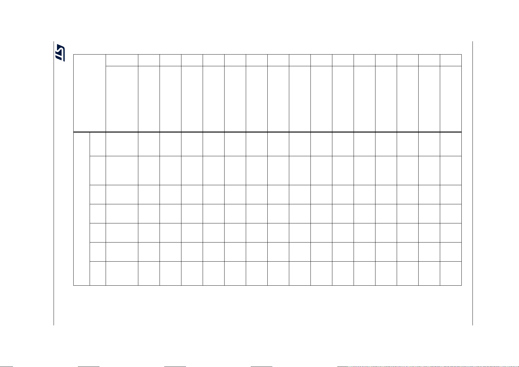
Table 9. STM32H725 pin alternate functions
AF0 AF1 AF2 AF3 AF4 AF5 AF6 AF7 AF8 AF9 AF10 AF11 AF12 AF13 AF14 AF15
STM32H725xE/G Pinouts, pin descriptions and alternate functions
DS13311 Rev 2 97/276
Port
PA0 -
PA1 -
PA2 -
Port A
PA3 -
PA4 D1 PWRE N -
PA5 D2 PWRE N
PA6 -
SYS
DFSDM1
FMC/LP
TIM1/SA
I4/TIM16
/17/TIM1
x/TIM2x
TIM2_C
H1/TIM2
_ETR
TIM2_CH2TIM5_CH2LPTIM3_
TIM2_CH3TIM5_CH3LPTIM4_
TIM2_CH4TIM5_CH4LPTIM5_
TIM2_C
H1/TIM2
_ETR
TIM1_B
FDCAN3
/PDM_S
AI1/TIM3
/4/5/12/1
TIM5_CH1TIM8_ETRTIM15_B
TIM5_ET
TIM3_CH1TIM8_B
KIN
/LCD/LP
TIM2/3/4
/5/LPUA
RT1/OC
TOSPIM
5
_P1/2/TI
M8
OUT
OUT
OUT
R
-
--
TIM8_C
H1N
KIN
CEC/DC
MI/PSSI/
DFSDM1
/I2C1/2/3
/4/5/LPTI
M2/OCT
OSPIM_
P1/TIM1
5/USAR
T1/10
TIM15_C
TIM15_C
TIM15_CH2I2S6_M
KIN
H1N
H1
CEC/FD
CAN3/S
PI1/I2S1/
SPI2/I2S
2/SPI3/I2
S3/SPI4/
5/6
SPI6_NS
S/I2S6_
WS
--
-
CK
SPI1_NS
S/I2S1_
WS
SPI1_SC
-
K/I2S1_
CK
SPI1_MI
-
SO/I2S1
_SDI
DFSDM1
/I2C4/5/
OCTOS
PIM_P1/
SAI1/SPI
3/I2S3/U
ART4
OCTOS
PIM_P1_
OCTOS
PIM_P1_
SPI3_NS
S/I2S3_
OCTOS
PIM_P1_
SDMMC
1/SPI2/I2
S2/SPI3/
I2S3/SPI
6/UART
7/USAR
T1/2/3/6
USART2
_CTS/U
SART2_
NSS
USART2
_RTS/U
SART2_
DE
USART2
IO0
IO2
WS
IO3
_TX
USART2
_RX
USART2
_CK
--
-
FDCAN1
LPUART
1/SAI4/S
DMMC1/
SPDIFR
X1/SPI6/
UART4/
UART4_TXSDMMC
UART4_
SAI4_SC
SPI6_NS
S/I2S6_
SPI6_SC
K/I2S6_
SPI6_MI
SO/I2S6
/2/FMC/
LCD/OC
TOSPIM
_P1/2/S
AI4/SDM
MC2/SP
DIFRX1/
5/8
TIM13/1
2_CMD
OCTOS
PIM_P1_
RX
K_B
- LCD_B2
WS
CK
TIM13_C
_SDI
4
IO3
--
---
-
H1
DFSDM1
TIM8
0
MP12
/ETH/I2C
4/LCD/M
DIOS/O
CTOSPI
M_P1/S
DMMC2/
SWPMI1
/TIM1x/T
IM8/UAR
T7/9/US
ART10
_CRS
ETH_MII
_RX_CL
K/ETH_
RMII_RE
F_CLK
ETH_MDIOMDIOS_
ETH_MII
_COL
MDIOS_
MDC
CRS/FM
C/LCD/O
CTOSPI
M_P1/O
TG1_FS/
OTG1_H
S/SAI4/S
DMMC2/
SAI4_SD_BETH_MII
SAI4_M
CLK_B
OTG_HS
_ULPI_D
OTG_HS
_ULPI_CK-
TIM8_B
KIN_CO
FMC/LC
D/MDIO
S/OCTO
SPIM_P
1/SDMM
C1/TIM1
x/TIM8
FMC_A1
9
OCTOS
PIM_P1_
DQS
MDIO
OCTOS
PIM_P1_
CLK
FMC_D8
/FMC_A
D8
FMC_D9
/FMC_A
D9
TIM1_B
KIN_CO
MP12
COMP/D
CMI/PSS
I/LCD/TI
M1x/TIM
DCMI_H
SYNC/P
SSI_DE
PSSI_D1
DCMI_PI
XCLK/P
SSI_PD
LCD/TIM
24/UART5SYS
23
--
- LCD_R2
- LCD_R1
- LCD_B5
LCD_VS
YNC
LCD_R4
4
LCD_G2
CK
EVENTO
UT
EVENTO
UT
EVENTO
UT
EVENTO
UT
EVENTO
UT
EVENTO
UT
EVENTO
UT

98/276 DS13311 Rev 2
Table 9. STM32H725 pin alternate functions (continued)
AF0 AF1 AF2 AF3 AF4 AF5 AF6 AF7 AF8 AF9 AF10 AF11 AF12 AF13 AF14 AF15
Pinouts, pin descriptions and alternate functions STM32H725xE/G
DFSDM1
/ETH/I2C
4/LCD/M
DIOS/O
CTOSPI
M_P1/S
DMMC2/
SWPMI1
/TIM1x/T
IM8/UAR
TIM8
T7/9/US
ART10
ETH_MII
_RX_DV
/ETH_R
IO2
MII_CRS
_SOF
UART7_
ETH_TX
MDIOS_
_ID
MDIO
- - - - LCD_R4
--
UART7_
_DV
RX
_ER
TX
FMC/LC
D/MDIO
S/OCTO
SPIM_P
1/SDMM
C1/TIM1
x/TIM8
FMC_SD
TIM8_B
KIN2_C
OMP12
LCD_B4
TIM1_B
COMP/D
CMI/PSS
I/LCD/TI
M1x/TIM
23
NWE
-
KIN2
- - LCD_B6
-
LCD_B3 LCD_R6
DCMI_D
0/PSSI_D0LCD_R5
DCMI_D
1/PSSI_D1LCD_B1
- LCD_R5
M8
H1N
KIN2
_DE
CEC/DC
MI/PSSI/
DFSDM1
/I2C1/2/3
/4/5/LPTI
M2/OCT
OSPIM_
P1/TIM1
5/USAR
T1/10
I2C3_SC
I2C3_S
CEC/FD
CAN3/S
PI1/I2S1/
SPI2/I2S
2/SPI3/I2
S3/SPI4/
SPI1_M
-
OSI/I2S1
L
SPI2_SC
MBA
K/I2S2_
---
SPI2_NS
-
S/I2S2_
SPI2_SC
-
K/I2S2_
SPI1_NS
S/I2S1_
5/6
_SDO
-
CK
WS
CK
WS
DFSDM1
/I2C4/5/
OCTOS
PIM_P1/
SAI1/SPI
3/I2S3/U
ART4
--
I2C5_SCLUSART1
I2C5_S
MBA
UART4_
RX
UART4_
TX
SPI3_NS
S/I2S3_
WS
SDMMC
1/SPI2/I2
S2/SPI3/
I2S3/SPI
6/UART
7/USAR
T1/2/3/6
_CK
USART1
_TX
USART1
_RX
USART1
_CTS/U
SART1_
NSS
USART1
_RTS/U
SART1_
DE
SPI6_NS
S/I2S6_
WS
LPUART
1/SAI4/S
DMMC1/
SPDIFR
X1/SPI6/
UART4/
SPI6_M
OSI/I2S6
_SDO
SAI4_FS_BFDCAN1
UART4_
RTS/UA
RT4_DE
DFSDM1
Port
SYS
PA7 -
PA8 M CO1
PA9 -
PA1 0 -
Port A
PA11 -
PA1 2 -
PA13JTMS/SWDIO--------------
PA14JTCK/SWCLK--------------
PA1 5 JTD I
FMC/LP
TIM1/SA
I4/TIM16
/17/TIM1
x/TIM2x
TIM1_C
TIM1_C
TIM1_C
TIM1_C
TIM1_C
TIM1_ET
TIM2_C
H1/TIM2
H1N
H1
H2
H3
H4
R
_ETR
FDCAN3
/PDM_S
AI1/TIM3
/4/5/12/1
TIM3_CH2TIM8_C
/LCD/LP
TIM2/3/4
/5/LPUA
RT1/OC
TOSPIM
5
_P1/2/TI
TIM8_B
-
LPUART
1_TX
LPUART
1_RX
LPUART
-
1_CTS
LPUART
1_RTS/L
-
PUART1
--CEC
FDCAN1
/2/FMC/
LCD/OC
TOSPIM
_P1/2/S
AI4/SDM
MC2/SP
DIFRX1/
5/8
TIM13/1
TIM14_C
--
---
--
FDCAN1
-
LCD_R3 -
4
H1
_RX
_TX
CRS/FM
C/LCD/O
CTOSPI
M_P1/O
TG1_FS/
OTG1_H
S/SAI4/S
DMMC2/
OCTOS
PIM_P1_
OTG_HS
OTG_HS
LCD/TIM
24/UART5SYS
LCD_VS
YNC
EVENTO
UT
EVENTO
UT
EVENTO
UT
EVENTO
UT
EVENTO
UT
EVENTO
UT
EVENTO
UT
EVENTO
UT
EVENTO
UT

Table 9. STM32H725 pin alternate functions (continued)
AF0 AF1 AF2 AF3 AF4 AF5 AF6 AF7 AF8 AF9 AF10 AF11 AF12 AF13 AF14 AF15
STM32H725xE/G Pinouts, pin descriptions and alternate functions
DS13311 Rev 2 99/276
Port B
Port
PB0 -
PB1 -
PB2 RTC_OUT SAI4_D1 SAI1_D1 -
PB3
PB4 NJTRST
PB5 -
PB6 -
PB7 -
PB8 -
SYS
JTDO/TRACE
SWO
FMC/LP
TIM1/SA
I4/TIM16
/17/TIM1
x/TIM2x
TIM1_C
TIM1_C
TIM2_C
TIM16_B
TIM17_B
TIM16_C
TIM17_C
TIM16_CH1TIM4_CH3DFSDM1
H2N
H3N
H2
KIN
KIN
H1N
H1N
FDCAN3
/PDM_S
AI1/TIM3
/4/5/12/1
5
TIM3_CH3TIM8_C
TIM3_CH4TIM8_C
---
TIM3_C
H1
TIM3_C
H2
TIM4_C
H1
TIM4_C
H2
DFSDM1
/LCD/LP
TIM2/3/4
/5/LPUA
RT1/OC
TOSPIM
_P1/2/TI
LCD_B5
_CKIN7
CEC/DC
MI/PSSI/
DFSDM1
/I2C1/2/3
/4/5/LPTI
M2/OCT
OSPIM_
P1/TIM1
M8
5/USAR
T1/10
OCTOS
PIM_P1_
H2N
H3N
--
-
-
IO1
OCTOS
PIM_P1_
IO0
DFSDM1
_CKIN1
I2C1_S
MBA
I2C1_SC
L
I2C1_SD
A
I2C1_SC
L
CEC/FD
CAN3/S
PI1/I2S1/
SPI2/I2S
2/SPI3/I2
S3/SPI4/
5/6
-
-
-
SPI1_SC
K/I2S1_
CK
SPI1_MI
SO/I2S1
_SDI
SPI1_M
OSI/I2S1
_SDO
CEC
-
-
DFSDM1
/I2C4/5/
OCTOS
PIM_P1/
SAI1/SPI
3/I2S3/U
DFSDM1
_CKOUT
DFSDM1
_DATIN1
SAI1_SD
SPI3_SC
K/I2S3_
SPI3_MI
SO/I2S3
I2C4_S
I2C4_SCLUSART1
I2C4_SD
I2C4_SCLSDMMC
ART4
_A
CK
_SDI
MBA
A
SDMMC
1/SPI2/I2
S2/SPI3/
I2S3/SPI
6/UART
7/USAR
T1/2/3/6
-
- - LCD_R6
SPI3_M
OSI/I2S3
_SDO
-
SPI2_NS
S/I2S2_
WS
SPI3_M
OSI/I2S3
_SDO
_TX
USART1
_RX
1_CKIN
FDCAN1
5/8
CTS
_A
CK
_SDI
/2/FMC/
LCD/OC
TOSPIM
_P1/2/S
AI4/SDM
MC2/SP
DIFRX1/
TIM13/1
4
LCD_R3
OCTOS
PIM_P1_
CLK
SDMMC
2_D2
SDMMC
2_D3
FDCAN2
_RX
FDCAN2
_TX
--
_RX
LPUART
1/SAI4/S
DMMC1/
SPDIFR
X1/SPI6/
UART4/
UART4_
SAI4_SD
SPI6_SC
K/I2S6_
SPI6_MI
SO/I2S6
SPI6_M
OSI/I2S6
_SDO
LPUART
1_TX
LPUART
1_RX
UART4_RXFDCAN1
DFSDM1
TIM8
1
2
DQS
-
7
NCS
2_D4
/ETH/I2C
4/LCD/M
DIOS/O
CTOSPI
M_P1/S
DMMC2/
SWPMI1
/TIM1x/T
IM8/UAR
T7/9/US
ART10
ETH_MII
_RXD2
ETH_MII
_RXD3
ETH_TX
_ER
RX
UART7_
TX
ETH_PP
S_OUT
DFSDM1
_DATIN5
DFSDM1
_CKIN5
ETH_MII
_TXD3
CRS/FM
C/LCD/O
CTOSPI
M_P1/O
TG1_FS/
OTG1_H
S/SAI4/S
DMMC2/
OTG_HS
_ULPI_D
OTG_HS
_ULPI_D
OCTOS
PIM_P1_
CRS_SYNCUART7_
OTG_HS
_ULPI_D
OCTOS
PIM_P1_
SDMMC
FMC/LC
D/MDIO
S/OCTO
SPIM_P
1/SDMM
C1/TIM1
x/TIM8
FMC_SD
CKE1
FMC_SD
FMC_NL
SDMMC
COMP/D
CMI/PSS
I/LCD/TI
M1x/TIM
- - LCD_G1
- - LCD_G0
TIM23_E
-
--
---
DCMI_D
10/PSSI
DCMI_D
5/PSSI_
NE1
DCMI_V
SYNC/P
SSI_RD
DCMI_D
1_D4
6/PSSI_D6LCD_B6
23
TR
_D10
D5
Y
LCD/TIM
24/UART5SYS
-
TIM24_ETREVENTO
UART5_RXEVENTO
UART5_TXEVENTO
-
EVENTO
UT
EVENTO
UT
EVENTO
UT
UT
EVENTO
UT
UT
UT
EVENTO
UT
EVENTO
UT
PB9 -
TIM17_CH1TIM4_CH4DFSDM1
_DATIN7
I2C1_SD
A
SPI2_NS
S/I2S2_
WS
I2C4_SDASDMMC
1_CDIR
UART4_TXFDCAN1
_TX
SDMMC
2_D5
I2C4_S
MBA
SDMMC
1_D5
DCMI_D
7/PSSI_D7LCD_B7
EVENTO
UT

100/276 DS13311 Rev 2
Table 9. STM32H725 pin alternate functions (continued)
AF0 AF1 AF2 AF3 AF4 AF5 AF6 AF7 AF8 AF9 AF10 AF11 AF12 AF13 AF14 AF15
Pinouts, pin descriptions and alternate functions STM32H725xE/G
Port
PB10 -
PB11 -
PB12 -
Port B
PB13 -
PB14 -
PB15 RTC_REFIN
SYS
FMC/LP
TIM1/SA
I4/TIM16
/17/TIM1
x/TIM2x
TIM2_C
H3
TIM2_C
H4
TIM1_B
KIN
TIM1_C
H1N
TIM1_C
H2N
TIM1_C
H3N
DFSDM1
FDCAN3
/PDM_S
AI1/TIM3
/4/5/12/1
TIM12_CH1TIM8_C
TIM12_CH2TIM8_C
/LCD/LP
TIM2/3/4
/5/LPUA
RT1/OC
TOSPIM
5
_P1/2/TI
M8
LPTIM2_
-
-
-
-
IN1
LPTIM2_
ETR
OCTOS
PIM_P1_
NCLK
LPTIM2_
OUT
H2N
H3N
CEC/DC
MI/PSSI/
DFSDM1
/I2C1/2/3
/4/5/LPTI
M2/OCT
OSPIM_
P1/TIM1
5/USAR
T1/10
I2C2_SC
L
I2C2_SD
A
I2C2_S
MBA
OCTOS
PIM_P1_
IO2
USART1
_TX
USART1
_RX
CEC/FD
CAN3/S
PI1/I2S1/
SPI2/I2S
2/SPI3/I2
S3/SPI4/
5/6
SPI2_SC
K/I2S2_
CK
-
SPI2_NS
S/I2S2_
WS
SPI2_SC
K/I2S2_
CK
SPI2_MI
SO/I2S2
_SDI
SPI2_M
OSI/I2S2
_SDO
DFSDM1
/I2C4/5/
OCTOS
PIM_P1/
SAI1/SPI
3/I2S3/U
ART4
DFSDM1
_DATIN7
DFSDM1
_CKIN7
DFSDM1
_DATIN1
DFSDM1
_CKIN1
DFSDM1
_DATIN2
DFSDM1
_CKIN2
SDMMC
1/SPI2/I2
S2/SPI3/
I2S3/SPI
6/UART
7/USAR
T1/2/3/6
USART3
_TX
USART3
_RX
USART3
_CK
USART3
_CTS/U
SART3_
NSS
USART3
_RTS/U
SART3_
DE
-
FDCAN1
LPUART
1/SAI4/S
DMMC1/
SPDIFR
X1/SPI6/
UART4/
UART4_
RTS/UA
RT4_DE
UART4_
/2/FMC/
LCD/OC
TOSPIM
_P1/2/S
AI4/SDM
MC2/SP
DIFRX1/
5/8
TIM13/1
4
OCTOS
-
PIM_P1_
NCS
--
FDCAN2
_RX
FDCAN2
_TX
SDMMC
2_D0
SDMMC
CTS
2_D1
DFSDM1
CRS/FM
C/LCD/O
CTOSPI
M_P1/O
TG1_FS/
OTG1_H
S/SAI4/S
DMMC2/
OTG_HS
_ULPI_D
OTG_HS
_ULPI_D
OTG_HS
_ULPI_D
OTG_HS
_ULPI_D
/ETH/I2C
4/LCD/M
DIOS/O
CTOSPI
M_P1/S
DMMC2/
SWPMI1
/TIM1x/T
IM8/UAR
TIM8
T7/9/US
ART10
ETH_MII
_RX_ER
3
ETH_MII
_TX_EN/
ETH_RM
4
II_TX_E
N
ETH_MII
_TXD0/E
TH_RMII
5
_TXD0
ETH_MII
_TXD1/E
TH_RMII
6
_TXD1
--
--
FMC/LC
D/MDIO
S/OCTO
SPIM_P
1/SDMM
C1/TIM1
x/TIM8
OCTOS
PIM_P1_
SDMMC
FMC_D1
0/FMC_
AD10
FMC_D1
1/FMC_
AD11
COMP/D
CMI/PSS
I/LCD/TI
M1x/TIM
23
- - LCD_G4
- - LCD_G5
TIM1_B
KIN_CO
IO0
1_D0
MP12
DCMI_D
2/PSSI_
D2
-
- LCD_G7
LCD/TIM
24/UART5SYS
EVENTO
UT
EVENTO
UT
UART5_RXEVENTO
UART5_TXEVENTO
LCD_CLKEVENTO
UT
UT
UT
EVENTO
UT
 Loading...