

STMicroelectronics STM32G0C1CC, STM32G0C1KC, STM32G0C1MC, STM32G0C1RC, STM32G0C1VC Datasheet
...
STM32G0C1xC/xE
Errata sheet
STM32G0C1xC/xE device errata
Applicability
This document applies to the part numbers of STM32G0C1xC/xE devices and the device variants as stated in this page.
It gives a summary and a description of the device errata, with respect to the device datasheet and reference manual RM0444.
Deviation of the real device behavior from the intended device behavior is considered to be a device limitation. Deviation of the
description in the reference manual or the datasheet from the intended device behavior is considered to be a documentation
erratum. The term “errata” applies both to limitations and documentation errata.
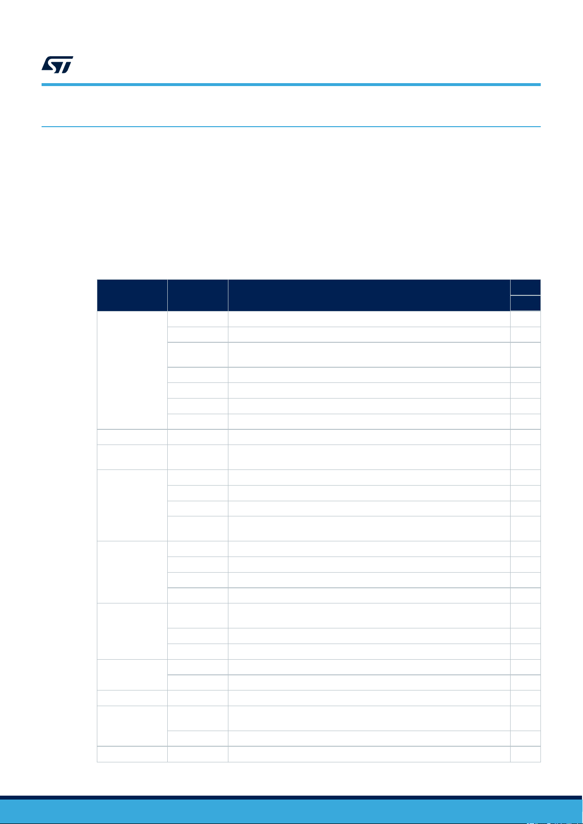
Table 1. Device summary
Reference Part numbers
STM32G0C1xC STM32G0C1CC, STM32G0C1KC, STM32G0C1MC, STM32G0C1RC ,STM32G0C1VC
STM32G0C1xE STM32G0C1CE, STM32G0C1KE, STM32G0C1ME, STM32G0C1NE, STM32G0C1RE, STM32G0C1VE
Table 2. Device variants
Reference
STM32G0C1xC/xE
1. Refer to the device datasheet for how to identify this code on different types of package.
2. REV_ID[15:0] bitfield of DBGMCU_IDCODE register.
Device marking
A 0x1000
Silicon revision codes
(1)
REV_ID
(2)
ES0549 - Rev 1 - January 2021
For further information contact your local STMicroelectronics sales office.
www.st.com
1 Summary of device errata
The following table gives a quick reference to the STM32G0C1xC/xE device limitations and their status:
A = workaround available
N = no workaround available
P = partial workaround available
Applicability of a workaround may depend on specific conditions of target application. Adoption of a workaround
may cause restrictions to target application. Workaround for a limitation is deemed partial if it only reduces the
rate of occurrence and/or consequences of the limitation, or if it is fully effective for only a subset of instances on
the device or in only a subset of operating modes, of the function concerned.
Table 3. Summary of device limitations
STM32G0C1xC/xE
Summary of device errata
Function
System
GPIO 2.3.1 Wakeup capability-enabled GPIOs not configurable after wakeup from Standby P
DMA 2.4.1
DMAMUX
ADC
TIM
LPTIM
RTC and TAMP 2.9.1 Calendar initialization may fail in case of consecutive INIT mode entry A
I2C
SPI
Section Limitation
2.2.1 Unstable LSI when it clocks RTC or CSS on LSE
2.2.2 WUFx wakeup flag wrongly set during configuration A
2.2.3
2.2.4 Wakeup from Stop not effective under certain conditions N
2.2.5 Flash memory PCROP area weakness N
2.2.6 PC13 signal transitions disturb LSE N
2.2.7 SRAM contents corrupted upon entry in Standby N
2.5.1 SOFx not asserted when writing into DMAMUX_CFR register N
2.5.2 OFx not asserted for trigger event coinciding with last DMAMUX request N
2.5.3 OFx not asserted when writing into DMAMUX_RGCFR register N
2.5.4
2.6.1 Overrun flag is not set if EOC reset coincides with new conversion end P
2.6.2 Writing ADC_CFGR1 register while ADEN bit is set resets RES[1:0] bitfield A
2.6.3 Out-of-threshold value is not detected in AWD1 Single mode A
2.6.4 ADC sampling time might be one cycle longer N
2.7.1
2.7.2 Consecutive compare event missed in specific conditions N
2.7.3 Output compare clear not working with external counter reset P
2.8.1 Device may remain stuck in LPTIM interrupt when entering Stop mode A
2.8.2 Device may remain stuck in LPTIM interrupt when clearing event flag P
2.10.1
2.10.2 Spurious bus error detection in master mode A
2.12.1 BSY bit may stay high when SPI is disabled A
Overwriting with all zeros a Flash memory location previously programmed with
all ones fails
DMA disable failure and error flag omission upon simultaneous transfer error
and global flag clear
Wrong input DMA request routed upon specific DMAMUX_CxCR register write
coinciding with synchronization event
One-pulse mode trigger not detected in master-slave reset + trigger
configuration
Wrong data sampling when data setup time (tSU;DAT) is shorter than one I2C
kernel clock period
Status
Rev. A
P
N
A
A
P
P
ES0549 - Rev 1
page 2/18
STM32G0C1xC/xE
Summary of device errata
Function Section Limitation
SPI
USART 2.11.1 Data corruption due to noisy receive line N
FDCAN
UCPD 2.14.1 UCPD transmitter output marginality at low temperature N
2.12.2 BSY bit may stay high at the end of data transfer in slave mode
2.13.1 Desynchronization under specific condition with edge filtering enabled A
2.13.2 Tx FIFO messages inverted under specific buffer usage and priority setting A
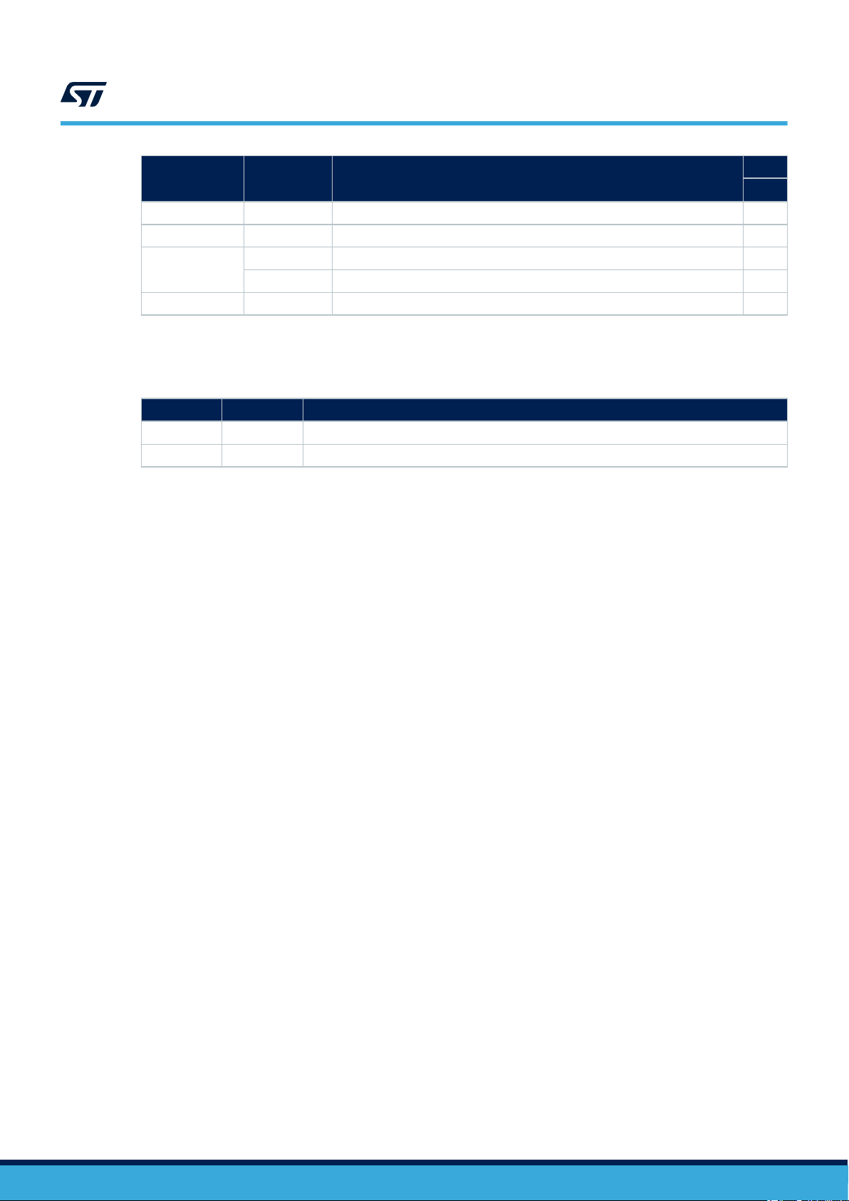
The following table gives a quick reference to the documentation errata.
Table 4. Summary of device documentation errata
Function Section Documentation erratum
System 2.2.8 Boot select after debug interface connection
USART 2.11.2 USART prescaler feature missing in USART implementation section
Status
Rev. A
A
ES0549 - Rev 1
page 3/18

STM32G0C1xC/xE
Description of device errata
2 Description of device errata
The following sections describe limitations of the applicable devices with Arm® core and provide workarounds if
available. They are grouped by device functions.
Note: Arm is a registered trademark of Arm Limited (or its subsidiaries) in the US and/or elsewhere.
2.1 Core
Reference manual and errata notice for the Arm® Cortex®-M0+ core revision r0p1 is available from http://
infocenter.arm.com.
2.2 System
2.2.1 Unstable LSI when it clocks RTC or CSS on LSE
Description
The LSI clock can become unstable (duty cycle different from 50 %) and its maximum frequency can become
significantly higher than 32 kHz, when:
• LSI clocks the RTC, or it clocks the clock security system (CSS) on LSE (which holds when the LSECSSON
bit set), and
• the VDD power domain is reset while the backup domain is not reset, which happens:
– upon exiting Shutdown mode
– if V
– if V
Workaround
Apply one of the following measures:
• Clock the RTC with LSE or HSE/32, without using the CSS on LSE
• If LSI clocks the RTC or when the LSECSSON bit is set, reset the backup domain upon each VDD power up
(when the BORRSTF flag is set). If V
registers and anti-tampering configuration.
is separate from VDD and VDD goes off then on
BAT
is tied to VDD (internally in the package for products not featuring the VBAT pin, or externally)
BAT
and a short (< 1 ms) VDD drop under VDD(min) occurs
is separate from VDD, also restore the RTC configuration, backup
BAT
2.2.2 WUFx wakeup flag wrongly set during configuration
Description
Upon configuring a wakeup pin (WKUPx), the corresponding wakeup flag (WUFx) might spuriously go high
depending on the state and configuration of the wakeup pin.
Workaround
After configuring a wakeup pin, clear its corresponding WUFx flag.
2.2.3 Overwriting with all zeros a Flash memory location previously programmed with all ones fails
Description
Any attempt to re-program with all zeros (0x0000 0000 0000 0000) a Flash memory location previously
programmed with 0xFFFF FFFF FFFF FFFF fails and the PROGERR flag of the FLASH_SR register is set.
ES0549 - Rev 1
page 4/18

Workaround
None.
2.2.4 Wakeup from Stop not effective under certain conditions
Description
With the HSI clock divider bitfield HSIDIV[2:0] set to a value different from 000, the device fails to enter Stop mode
when SYSCLK is set to HSE clock.
With the HSI clock divider bitfield HSIDIV[2:0] set to a value different from 000, peripherals with clock request
capability fail to wake the device up from Stop modes.
Workaround
None.
2.2.5 Flash memory PCROP area weakness
Description
When the CPU accesses PCROP-protected Flash memory areas:
• Fetch requests are allowed and are responded to normally.
• Read access are properly discarded. However, the bus holds and returns the value read during previous
successful access.
STM32G0C1xC/xE
System
Workaround
None.
Note: We recommend to use the PCROP protection in the following RDP and PCROP_RDP configurations:
• RDP = Level 1 and PCROP_RDP = 1
• RDP = Level 2
2.2.6 PC13 signal transitions disturb LSE
Description
The PC13 port toggling disturbs the LSE clock.
Workaround
None.
2.2.7 SRAM contents corrupted upon entry in Standby
Description
Entry of the device in Standby mode causes the SRAM content corruption.
Workaround
None.
2.2.8 Boot select after debug interface connection
Description
Some revisions of the reference manual may omit the following information.
ES0549 - Rev 1
page 5/18

STM32G0C1xC/xE
GPIO
After connecting the debug interface and until the device power-down, the boot source upon reset or wakeup from
a low-power mode is determined by the PA14-BOOT0 pin level before connecting the debug interface (stored by
the device), as opposed to the actual PA14-BOOT0 pin level. The device power-up restores the operation of the
PA14-BOOT0 pin as direct boot source selector.
This is a documentation issue rather than a device limitation.
Workaround
No application workaround is required or applicable.
2.3
GPIO
2.3.1 Wakeup capability-enabled GPIOs not configurable after wakeup from Standby
Description
After the devices wakes up from Standby mode, GPIOs with the wakeup capability enabled cannot further be
configured through the GPIO registers.
Workaround
Disable the wakeup capability of the GPIOs that must remain configurable through the GPIO registers after the
wakeup from Standby.
2.4
DMA
2.4.1 DMA disable failure and error flag omission upon simultaneous transfer error and global flag
clear
Description
Upon a data transfer error in a DMA channel x, both the specific TEIFx and the global GIFx flags are raised and
the channel x is normally automatically disabled. However, if in the same clock cycle the software clears the GIFx
flag (by setting the CGIFx bit of the DMA_IFCR register), the automatic channel disable fails and the TEIFx flag is
not raised.
This issue does not occur with ST's HAL software that does not use and clear the GIFx flag when the channel is
active.
Workaround
Do not clear GIFx flags when the channel is active. Instead, use HTIFx, TCIFx, and TEIFx specific event flags and
their corresponding clear bits.
2.5 DMAMUX
2.5.1 SOFx not asserted when writing into DMAMUX_CFR register
Description
The SOFx flag of the DMAMUX_CSR status register is not asserted if overrun from another DMAMUX channel
occurs when the software writes into the DMAMUX_CFR register.
This can happen when multiple DMA channels operate in synchronization mode, and when overrun can occur
from more than one channel. As the SOFx flag clear requires a write into the DMAMUX_CFR register (to set
the corresponding CSOFx bit), overrun occurring from another DMAMUX channel operating during that write
operation fails to raise its corresponding SOFx flag.
ES0549 - Rev 1
page 6/18
 Loading...