

STMicroelectronics STM32F722IC, STM32F722IE, STM32F722RC, STM32F722RE, STM32F722VC Datasheet
...
STM32F722xx
LQFP64 (10 × 10 mm)
UFBGA144 (7 x 7 mm)
UFBGA176 (10 x 10 mm)
LQFP176 (24 x 24 mm)
WLCSP100
(0.4 mm pitch)
LQFP144 (20 × 20 mm)
LQFP100 (14 × 14 mm)
STM32F723xx
Arm® Cortex®-M7 32b MCU+FPU, 462DMIPS, up to 512KB Flash
/256+16+4KB RAM, USB OTG HS/FS, 18 TIMs, 3 ADCs, 21 com IF
Datasheet - production data
Features
• Core: Arm® 32-bit Cortex®-M7 CPU with FPU,
adaptive real-time accelerator (ART
Accelerator) and L1-cache: 8 Kbytes of data
cache and 8 Kbytes of instruction cache,
allowing 0-wait state execution from embedded
Flash memory and external memories,
frequency up to 216 MHz, MPU,
462 DMIPS/2.14 DMIPS/MHz (Dhrystone 2.1)
and DSP instructions.
• Memories
– Up to 512 Kbytes of Flash memory with
protection mechanisms (read and write
protections, proprietary code readout
protection (PCROP))
– 528 bytes of OTP memory
– SRAM: 256 Kbytes (including 64 Kbytes of
data TCM RAM for critical real-time data) +
16 Kbytes of instruction TCM RAM (for
critical real-time routines) + 4 Kbytes of
backup SRAM (available in the lowest
power modes)
– Flexible external memory controller with up
to 32-bit data bus: SRAM, PSRAM,
SDRAM/LPSDR SDRAM, NOR/NAND
memories
• Dual mode Quad-SPI
• Clock, reset and supply management
– 1.7 V to 3.6 V application supply and I/Os
– POR, PDR, PVD and BOR
– Dedicated USB power
– 4-to-26 MHz crystal oscillator
– Internal 16 MHz factory-trimmed RC (1%
accuracy)
– 32 kHz oscillator for RTC with calibration
– Internal 32 kHz RC with calibration
• Low-power
– Sleep, Stop and Standby modes
–V
supply for RTC, 32×32 bit backup
BAT
registers + 4 Kbytes of backup SRAM
• 3×12-bit, 2.4 MSPS ADC: up to 24 channels
and 7.2 MSPS in triple interleaved mode
• 2×12-bit D/A converters
• Up to 18 timers: up to thirteen 16-bit (1x low-
power 16-bit timer available in Stop mode) and
two 32-bit timers, each with up to 4
IC/OC/PWMs or pulse counter and quadrature
(incremental) encoder inputs. All 15 timers
running up to 216 MHz. 2x watchdogs, SysTick
timer
• General-purpose DMA: 16-stream DMA
controller with FIFOs and burst support
• Debug mode
– SWD and JTAG interfaces
–Cortex
®
-M7 Trace Macrocell™
• Up to 140 I/O ports with interrupt capability
– Up to 136 fast I/Os up to 108 MHz
– Up to 138 5 V-tolerant I/Os
• Up to 21 communication interfaces
– Up to 3× I
2
C interfaces (SMBus/PMBus)
– Up to 4 USARTs/4 UARTs (27 Mbit/s,
ISO7816 interface, LIN, IrDA, modem
control)
– Up to 5 SPIs (up to 54 Mbit/s), 3 with
muxed simplex I
2
Ss for audio class
accuracy via internal audio PLL or external
clock
– 2 x SAIs (serial audio interface)
November 2020 DS11853 Rev 7 1/230
This is information on a product in full production.
www.st.com

STM32F722xx STM32F723xx
– 1 x CAN (2.0B active)
– 2 x SDMMCs
• Advanced connectivity
– USB 2.0 full-speed device/host/OTG
controller with on-chip PHY
– USB 2.0 high-speed/full-speed
device/host/OTG controller with
dedicated DMA, on-chip full-speed
PHY and on-chip Hi-speed PHY or
ULPI depending on the part number
• True random number generator
Table 1. Device summary
Reference Part number
STM32F722xx
STM32F723xx
STM32F722IC, STM32F722IE, STM32F722RC, STM32F722RE, STM32F722VC,
STM32F722VE, STM32F722ZC, STM32F722ZE
STM32F723IC, STM32F723IE, STM32F723VC, STM32F723VE, STM32F723ZC,
STM32F723ZE
• CRC calculation unit
• RTC: subsecond accuracy, hardware
calendar
• 96-bit unique ID
2/230 DS11853 Rev 7

STM32F722xx STM32F723xx Contents
Contents
1 Introduction . . . . . . . . . . . . . . . . . . . . . . . . . . . . . . . . . . . . . . . . . . . . . . . 13
2 Description . . . . . . . . . . . . . . . . . . . . . . . . . . . . . . . . . . . . . . . . . . . . . . . . 14
2.1 Full compatibility throughout the family . . . . . . . . . . . . . . . . . . . . . . . . . . 17
2.2 STM32F723xx versus STM32F722xx LQFP100/ LQFP144/
LQFP176 packages . . . . . . . . . . . . . . . . . . . . . . . . . . . . . . . . . . . . . . . . . 19
3 Functional overview . . . . . . . . . . . . . . . . . . . . . . . . . . . . . . . . . . . . . . . . 22
3.1 Arm® Cortex®-M7 with FPU . . . . . . . . . . . . . . . . . . . . . . . . . . . . . . . . . . . 22
3.2 Memory protection unit . . . . . . . . . . . . . . . . . . . . . . . . . . . . . . . . . . . . . . . 22
3.3 Embedded Flash memory . . . . . . . . . . . . . . . . . . . . . . . . . . . . . . . . . . . . 23
3.4 CRC (cyclic redundancy check) calculation unit . . . . . . . . . . . . . . . . . . . 23
3.5 Embedded SRAM . . . . . . . . . . . . . . . . . . . . . . . . . . . . . . . . . . . . . . . . . . . 23
3.6 AXI-AHB bus matrix . . . . . . . . . . . . . . . . . . . . . . . . . . . . . . . . . . . . . . . . . 24
3.7 DMA controller (DMA) . . . . . . . . . . . . . . . . . . . . . . . . . . . . . . . . . . . . . . . 25
3.8 Flexible memory controller (FMC) . . . . . . . . . . . . . . . . . . . . . . . . . . . . . . 26
3.9 Quad-SPI memory interface (QUADSPI) . . . . . . . . . . . . . . . . . . . . . . . . . 26
3.10 Nested vectored interrupt controller (NVIC) . . . . . . . . . . . . . . . . . . . . . . . 27
3.11 External interrupt/event controller (EXTI) . . . . . . . . . . . . . . . . . . . . . . . . . 27
3.12 Clocks and startup . . . . . . . . . . . . . . . . . . . . . . . . . . . . . . . . . . . . . . . . . . 27
3.13 Boot modes . . . . . . . . . . . . . . . . . . . . . . . . . . . . . . . . . . . . . . . . . . . . . . . 28
3.14 Power supply schemes . . . . . . . . . . . . . . . . . . . . . . . . . . . . . . . . . . . . . . 28
3.15 Power supply supervisor . . . . . . . . . . . . . . . . . . . . . . . . . . . . . . . . . . . . . 30
3.15.1 Internal reset ON . . . . . . . . . . . . . . . . . . . . . . . . . . . . . . . . . . . . . . . . . . 30
3.15.2 Internal reset OFF . . . . . . . . . . . . . . . . . . . . . . . . . . . . . . . . . . . . . . . . . 30
3.16 Voltage regulator . . . . . . . . . . . . . . . . . . . . . . . . . . . . . . . . . . . . . . . . . . . 32
3.16.1 Regulator ON . . . . . . . . . . . . . . . . . . . . . . . . . . . . . . . . . . . . . . . . . . . . . 32
3.16.2 Regulator OFF . . . . . . . . . . . . . . . . . . . . . . . . . . . . . . . . . . . . . . . . . . . . 33
3.16.3 Regulator ON/OFF and internal reset ON/OFF availability . . . . . . . . . . 36
3.17 Real-time clock (RTC), backup SRAM and backup registers . . . . . . . . . . 36
3.18 Low-power modes . . . . . . . . . . . . . . . . . . . . . . . . . . . . . . . . . . . . . . . . . . 37
3.19 V
operation . . . . . . . . . . . . . . . . . . . . . . . . . . . . . . . . . . . . . . . . . . . . . 38
BAT
DS11853 Rev 7 3/230
6

Contents STM32F722xx STM32F723xx
3.20 Timers and watchdogs . . . . . . . . . . . . . . . . . . . . . . . . . . . . . . . . . . . . . . . 38
3.20.1 Advanced-control timers (TIM1, TIM8) . . . . . . . . . . . . . . . . . . . . . . . . . 40
3.20.2 General-purpose timers (TIMx) . . . . . . . . . . . . . . . . . . . . . . . . . . . . . . . 40
3.20.3 Basic timers TIM6 and TIM7 . . . . . . . . . . . . . . . . . . . . . . . . . . . . . . . . . 40
3.20.4 Low-power timer (LPTIM1) . . . . . . . . . . . . . . . . . . . . . . . . . . . . . . . . . . 41
3.20.5 Independent watchdog . . . . . . . . . . . . . . . . . . . . . . . . . . . . . . . . . . . . . 41
3.20.6 Window watchdog . . . . . . . . . . . . . . . . . . . . . . . . . . . . . . . . . . . . . . . . . 41
3.20.7 SysTick timer . . . . . . . . . . . . . . . . . . . . . . . . . . . . . . . . . . . . . . . . . . . . . 41
3.21 Inter-integrated circuit interface (I2C) . . . . . . . . . . . . . . . . . . . . . . . . . . . . 42
3.22 Universal synchronous/asynchronous receiver transmitters (USART) . . 43
3.23 Serial peripheral interface (SPI)/inter- integrated sound interfaces (I2S) . 44
3.24 Serial audio interface (SAI) . . . . . . . . . . . . . . . . . . . . . . . . . . . . . . . . . . . 44
3.25 Audio PLL (PLLI2S) . . . . . . . . . . . . . . . . . . . . . . . . . . . . . . . . . . . . . . . . . 45
3.26 Audio PLL (PLLSAI) . . . . . . . . . . . . . . . . . . . . . . . . . . . . . . . . . . . . . . . . . 45
3.27 SD/SDIO/MMC card host interface (SDMMC) . . . . . . . . . . . . . . . . . . . . . 45
3.28 Controller area network (bxCAN) . . . . . . . . . . . . . . . . . . . . . . . . . . . . . . . 45
3.29 Universal serial bus on-the-go full-speed (OTG_FS) . . . . . . . . . . . . . . . . 46
3.30 Universal serial bus on-the-go high-speed (OTG_HS) . . . . . . . . . . . . . . . 46
3.31 Random number generator (RNG) . . . . . . . . . . . . . . . . . . . . . . . . . . . . . . 47
3.32 General-purpose input/outputs (GPIOs) . . . . . . . . . . . . . . . . . . . . . . . . . . 47
3.33 Analog-to-digital converters (ADCs) . . . . . . . . . . . . . . . . . . . . . . . . . . . . . 47
3.34 Temperature sensor . . . . . . . . . . . . . . . . . . . . . . . . . . . . . . . . . . . . . . . . . 48
3.35 Digital-to-analog converter (DAC) . . . . . . . . . . . . . . . . . . . . . . . . . . . . . . 48
3.36 Serial wire JTAG debug port (SWJ-DP) . . . . . . . . . . . . . . . . . . . . . . . . . . 48
3.37 Embedded Trace Macrocell™ . . . . . . . . . . . . . . . . . . . . . . . . . . . . . . . . . 49
4 Pinouts and pin description . . . . . . . . . . . . . . . . . . . . . . . . . . . . . . . . . . 50
5 Memory mapping . . . . . . . . . . . . . . . . . . . . . . . . . . . . . . . . . . . . . . . . . . 100
6 Electrical characteristics . . . . . . . . . . . . . . . . . . . . . . . . . . . . . . . . . . . 101
6.1 Parameter conditions . . . . . . . . . . . . . . . . . . . . . . . . . . . . . . . . . . . . . . . 101
6.1.1 Minimum and maximum values . . . . . . . . . . . . . . . . . . . . . . . . . . . . . . 101
6.1.2 Typical values . . . . . . . . . . . . . . . . . . . . . . . . . . . . . . . . . . . . . . . . . . . 101
6.1.3 Typical curves . . . . . . . . . . . . . . . . . . . . . . . . . . . . . . . . . . . . . . . . . . . 101
4/230 DS11853 Rev 7

STM32F722xx STM32F723xx Contents
6.1.4 Loading capacitor . . . . . . . . . . . . . . . . . . . . . . . . . . . . . . . . . . . . . . . . 101
6.1.5 Pin input voltage . . . . . . . . . . . . . . . . . . . . . . . . . . . . . . . . . . . . . . . . . 101
6.1.6 Power supply scheme . . . . . . . . . . . . . . . . . . . . . . . . . . . . . . . . . . . . . 102
6.1.7 Current consumption measurement . . . . . . . . . . . . . . . . . . . . . . . . . . 104
6.2 Absolute maximum ratings . . . . . . . . . . . . . . . . . . . . . . . . . . . . . . . . . . . 104
6.3 Operating conditions . . . . . . . . . . . . . . . . . . . . . . . . . . . . . . . . . . . . . . . 106
6.3.1 General operating conditions . . . . . . . . . . . . . . . . . . . . . . . . . . . . . . . . 106
6.3.2 VCAP1/VCAP2 external capacitor . . . . . . . . . . . . . . . . . . . . . . . . . . . . 109
6.3.3 Operating conditions at power-up / power-down (regulator ON) . . . . . 110
6.3.4 Operating conditions at power-up / power-down (regulator OFF) . . . . 110
6.3.5 Reset and power control block characteristics . . . . . . . . . . . . . . . . . . 110
6.3.6 Over-drive switching characteristics . . . . . . . . . . . . . . . . . . . . . . . . . . 112
6.3.7 Supply current characteristics . . . . . . . . . . . . . . . . . . . . . . . . . . . . . . . 112
6.3.8 Wakeup time from low-power modes . . . . . . . . . . . . . . . . . . . . . . . . . . 130
6.3.9 External clock source characteristics . . . . . . . . . . . . . . . . . . . . . . . . . . 131
6.3.10 Internal clock source characteristics . . . . . . . . . . . . . . . . . . . . . . . . . . 136
6.3.11 PLL characteristics . . . . . . . . . . . . . . . . . . . . . . . . . . . . . . . . . . . . . . . . 137
6.3.12 PLL spread spectrum clock generation (SSCG) characteristics . . . . . 140
6.3.13 USB OTG HS PHY PLLs characteristics (on STM32F723xx devices) 142
6.3.14 USB OTG HS PHY regulator characteristics . . . . . . . . . . . . . . . . . . . 142
6.3.15 USB HS PHY external resistor characteristics
(on STM32F723xx devices) . . . . . . . . . . . . . . . . . . . . . . . . . . . . . . . . . 143
6.3.16 Memory characteristics . . . . . . . . . . . . . . . . . . . . . . . . . . . . . . . . . . . . 143
6.3.17 EMC characteristics . . . . . . . . . . . . . . . . . . . . . . . . . . . . . . . . . . . . . . . 145
6.3.18 Absolute maximum ratings (electrical sensitivity) . . . . . . . . . . . . . . . . 146
6.3.19 I/O current injection characteristics . . . . . . . . . . . . . . . . . . . . . . . . . . . 147
6.3.20 I/O port characteristics . . . . . . . . . . . . . . . . . . . . . . . . . . . . . . . . . . . . . 148
6.3.21 NRST pin characteristics . . . . . . . . . . . . . . . . . . . . . . . . . . . . . . . . . . . 154
6.3.22 TIM timer characteristics . . . . . . . . . . . . . . . . . . . . . . . . . . . . . . . . . . . 155
6.3.23 RTC characteristics . . . . . . . . . . . . . . . . . . . . . . . . . . . . . . . . . . . . . . . 155
6.3.24 12-bit ADC characteristics . . . . . . . . . . . . . . . . . . . . . . . . . . . . . . . . . . 155
6.3.25 Temperature sensor characteristics . . . . . . . . . . . . . . . . . . . . . . . . . . . 161
6.3.26 V
monitoring characteristics . . . . . . . . . . . . . . . . . . . . . . . . . . . . . . 161
BAT
6.3.27 Reference voltage . . . . . . . . . . . . . . . . . . . . . . . . . . . . . . . . . . . . . . . . 161
6.3.28 DAC electrical characteristics . . . . . . . . . . . . . . . . . . . . . . . . . . . . . . . 162
6.3.29 Communications interfaces . . . . . . . . . . . . . . . . . . . . . . . . . . . . . . . . . 164
6.3.30 FMC characteristics . . . . . . . . . . . . . . . . . . . . . . . . . . . . . . . . . . . . . . . 177
DS11853 Rev 7 5/230
6

Contents STM32F722xx STM32F723xx
6.3.31 Quad-SPI interface characteristics . . . . . . . . . . . . . . . . . . . . . . . . . . . 197
6.3.32 SD/SDIO MMC card host interface (SDMMC) characteristics . . . . . . . 199
7 Package information . . . . . . . . . . . . . . . . . . . . . . . . . . . . . . . . . . . . . . . 202
7.1 LQFP64 – 10 x 10 mm, low-profile quad flat package information . . . . . 202
7.2 LQFP100, 14 x 14 mm low-profile quad flat package information . . . . . 205
7.3 LQFP144, 20 x 20 mm low-profile quad flat package information . . . . . 208
7.4 LQFP176 24 x 24 mm low-profile quad flat package information . . . . . . .211
7.5 UFBGA144 package information . . . . . . . . . . . . . . . . . . . . . . . . . . . . . . 215
7.6 UFBGA176+25, 10 x 10, 0.65 mm ultra thin-pitch ball grid
array package information . . . . . . . . . . . . . . . . . . . . . . . . . . . . . . . . . . . 218
7.7 WLCSP100 - 0.4 mm pitch wafer level chip scale package information 221
7.8 Thermal characteristics . . . . . . . . . . . . . . . . . . . . . . . . . . . . . . . . . . . . . 225
8 Ordering information . . . . . . . . . . . . . . . . . . . . . . . . . . . . . . . . . . . . . . 226
Appendix A Recommendations when using internal reset OFF . . . . . . . . . . . 227
A.1 Operating conditions . . . . . . . . . . . . . . . . . . . . . . . . . . . . . . . . . . . . . . . . 227
Revision history . . . . . . . . . . . . . . . . . . . . . . . . . . . . . . . . . . . . . . . . . . . . . . . . . . . 228
6/230 DS11853 Rev 7

STM32F722xx STM32F723xx List of tables
List of tables
Table 1. Device summary . . . . . . . . . . . . . . . . . . . . . . . . . . . . . . . . . . . . . . . . . . . . . . . . . . . . . . . . . . 2
Table 2. STM32F722xx and STM32F723xx features and peripheral counts . . . . . . . . . . . . . . . . . . 15
Table 3. Voltage regulator configuration mode versus device operating mode . . . . . . . . . . . . . . . . 33
Table 4. Regulator ON/OFF and internal reset ON/OFF availability. . . . . . . . . . . . . . . . . . . . . . . . . 36
Table 5. Voltage regulator modes in stop mode . . . . . . . . . . . . . . . . . . . . . . . . . . . . . . . . . . . . . . . . 37
Table 6. Timer feature comparison . . . . . . . . . . . . . . . . . . . . . . . . . . . . . . . . . . . . . . . . . . . . . . . . . . 39
Table 7. I2C implementation . . . . . . . . . . . . . . . . . . . . . . . . . . . . . . . . . . . . . . . . . . . . . . . . . . . . . . . 42
Table 8. USART implementation . . . . . . . . . . . . . . . . . . . . . . . . . . . . . . . . . . . . . . . . . . . . . . . . . . . 43
Table 9. Legend/abbreviations used in the pinout table . . . . . . . . . . . . . . . . . . . . . . . . . . . . . . . . . . 61
Table 10. STM32F722xx and STM32F723xx pin and ball definition . . . . . . . . . . . . . . . . . . . . . . . . . 62
Table 11. FMC pin definition. . . . . . . . . . . . . . . . . . . . . . . . . . . . . . . . . . . . . . . . . . . . . . . . . . . . . . . . 86
Table 12. STM32F722xx and STM32F723xx alternate function mapping. . . . . . . . . . . . . . . . . . . . . 89
Table 13. Voltage characteristics . . . . . . . . . . . . . . . . . . . . . . . . . . . . . . . . . . . . . . . . . . . . . . . . . . . 104
Table 14. Current characteristics . . . . . . . . . . . . . . . . . . . . . . . . . . . . . . . . . . . . . . . . . . . . . . . . . . . 105
Table 15. Thermal characteristics. . . . . . . . . . . . . . . . . . . . . . . . . . . . . . . . . . . . . . . . . . . . . . . . . . . 106
Table 16. General operating conditions . . . . . . . . . . . . . . . . . . . . . . . . . . . . . . . . . . . . . . . . . . . . . . 106
Table 17. Limitations depending on the operating power supply range . . . . . . . . . . . . . . . . . . . . . . 108
Table 18. VCAP1/VCAP2 operating conditions . . . . . . . . . . . . . . . . . . . . . . . . . . . . . . . . . . . . . . . . 109
Table 19. VCAP1 operating conditions in the LQFP64 package . . . . . . . . . . . . . . . . . . . . . . . . . . . 110
Table 20. Operating conditions at power-up / power-down (regulator ON) . . . . . . . . . . . . . . . . . . . 110
Table 21. Operating conditions at power-up / power-down (regulator OFF). . . . . . . . . . . . . . . . . . . 110
Table 22. reset and power control block characteristics . . . . . . . . . . . . . . . . . . . . . . . . . . . . . . . . . 111
Table 23. Over-drive switching characteristics . . . . . . . . . . . . . . . . . . . . . . . . . . . . . . . . . . . . . . . . . 112
Table 24. Typical and maximum current consumption in Run mode, code with data processing
running from ITCM RAM, regulator ON . . . . . . . . . . . . . . . . . . . . . . . . . . . . . . . . . . . . . . 113
Table 25. Typical and maximum current consumption in Run mode, code with data processing
running from Flash memory (ART ON except prefetch / L1-cache ON)
or SRAM on AXI (L1-cache ON), regulator ON . . . . . . . . . . . . . . . . . . . . . . . . . . . . . . . . 114
Table 26. Typical and maximum current consumption in Run mode, code with data processing
running from Flash memory or SRAM on AXI (L1-cache disabled), regulator ON . . . . . 115
Table 27. Typical and maximum current consumption in Run mode, code with data processing
running from Flash memory on ITCM interface (ART disabled), regulator ON . . . . . . . . 116
Table 28. Typical and maximum current consumption in Run mode, code with data processing
running from Flash memory (ART ON except prefetch / L1-cache ON)
or SRAM on AXI (L1-cache ON), regulator OFF. . . . . . . . . . . . . . . . . . . . . . . . . . . . . . . . 117
Table 29. Typical and maximum current consumption in Sleep mode, regulator ON. . . . . . . . . . . . 118
Table 30. Typical and maximum current consumption in Sleep mode, regulator OFF . . . . . . . . . . . 118
Table 31. Typical and maximum current consumptions in Stop mode . . . . . . . . . . . . . . . . . . . . . . . 119
Table 32. Typical and maximum current consumptions in Standby mode . . . . . . . . . . . . . . . . . . . . 120
Table 33. Typical and maximum current consumptions in V
Table 34. Switching output I/O current consumption . . . . . . . . . . . . . . . . . . . . . . . . . . . . . . . . . . . . 125
Table 35. Peripheral current consumption . . . . . . . . . . . . . . . . . . . . . . . . . . . . . . . . . . . . . . . . . . . . 127
Table 36. USB OTG HS and USB OTG PHY HS current consumption . . . . . . . . . . . . . . . . . . . . . . 130
Table 37. Low-power mode wakeup timings . . . . . . . . . . . . . . . . . . . . . . . . . . . . . . . . . . . . . . . . . . 130
Table 38. High-speed external user clock characteristics. . . . . . . . . . . . . . . . . . . . . . . . . . . . . . . . . 131
Table 39. Low-speed external user clock characteristics . . . . . . . . . . . . . . . . . . . . . . . . . . . . . . . . . 132
Table 40. HSE 4-26 MHz oscillator characteristics. . . . . . . . . . . . . . . . . . . . . . . . . . . . . . . . . . . . . . 133
Table 41. LSE oscillator characteristics (f
= 32.768 kHz) . . . . . . . . . . . . . . . . . . . . . . . . . . . . . . 134
LSE
mode. . . . . . . . . . . . . . . . . . . . . . . 121
BAT
DS11853 Rev 7 7/230
9

List of tables STM32F722xx STM32F723xx
Table 42. HSI oscillator characteristics . . . . . . . . . . . . . . . . . . . . . . . . . . . . . . . . . . . . . . . . . . . . . . 136
Table 43. LSI oscillator characteristics . . . . . . . . . . . . . . . . . . . . . . . . . . . . . . . . . . . . . . . . . . . . . . 137
Table 44. Main PLL characteristics. . . . . . . . . . . . . . . . . . . . . . . . . . . . . . . . . . . . . . . . . . . . . . . . . . 137
Table 45. PLLI2S characteristics . . . . . . . . . . . . . . . . . . . . . . . . . . . . . . . . . . . . . . . . . . . . . . . . . . . 138
Table 46. PLLISAI characteristics. . . . . . . . . . . . . . . . . . . . . . . . . . . . . . . . . . . . . . . . . . . . . . . . . . . 139
Table 47. SSCG parameters constraint . . . . . . . . . . . . . . . . . . . . . . . . . . . . . . . . . . . . . . . . . . . . . . 140
Table 48. USB OTG HS PLL1 characteristics . . . . . . . . . . . . . . . . . . . . . . . . . . . . . . . . . . . . . . . . . 142
Table 49. USB OTG HS PLL2 characteristics . . . . . . . . . . . . . . . . . . . . . . . . . . . . . . . . . . . . . . . . . 142
Table 50. USB OTG HS PHY regulator characteristics . . . . . . . . . . . . . . . . . . . . . . . . . . . . . . . . . . 142
Table 51. USB HS PHY external resistor characteristics (on STM32F723xx devices). . . . . . . . . . . 143
Table 52. Flash memory characteristics . . . . . . . . . . . . . . . . . . . . . . . . . . . . . . . . . . . . . . . . . . . . . . 143
Table 53. Flash memory programming. . . . . . . . . . . . . . . . . . . . . . . . . . . . . . . . . . . . . . . . . . . . . . . 143
Table 54. Flash memory programming with VPP . . . . . . . . . . . . . . . . . . . . . . . . . . . . . . . . . . . . . . . 144
Table 55. Flash memory endurance and data retention. . . . . . . . . . . . . . . . . . . . . . . . . . . . . . . . . . 144
Table 56. EMS characteristics . . . . . . . . . . . . . . . . . . . . . . . . . . . . . . . . . . . . . . . . . . . . . . . . . . . . . 145
Table 57. EMI characteristics . . . . . . . . . . . . . . . . . . . . . . . . . . . . . . . . . . . . . . . . . . . . . . . . . . . . . . 146
Table 58. ESD absolute maximum ratings . . . . . . . . . . . . . . . . . . . . . . . . . . . . . . . . . . . . . . . . . . . . 147
Table 59. Electrical sensitivities . . . . . . . . . . . . . . . . . . . . . . . . . . . . . . . . . . . . . . . . . . . . . . . . . . . . 147
Table 60. I/O current injection susceptibility . . . . . . . . . . . . . . . . . . . . . . . . . . . . . . . . . . . . . . . . . . . 148
Table 61. I/O static characteristics . . . . . . . . . . . . . . . . . . . . . . . . . . . . . . . . . . . . . . . . . . . . . . . . . . 148
Table 62. Output voltage characteristics . . . . . . . . . . . . . . . . . . . . . . . . . . . . . . . . . . . . . . . . . . . . . 151
Table 63. I/O AC characteristics . . . . . . . . . . . . . . . . . . . . . . . . . . . . . . . . . . . . . . . . . . . . . . . . . . . . 152
Table 64. NRST pin characteristics . . . . . . . . . . . . . . . . . . . . . . . . . . . . . . . . . . . . . . . . . . . . . . . . . 154
Table 65. TIMx characteristics . . . . . . . . . . . . . . . . . . . . . . . . . . . . . . . . . . . . . . . . . . . . . . . . . . . . . 155
Table 66. RTC characteristics . . . . . . . . . . . . . . . . . . . . . . . . . . . . . . . . . . . . . . . . . . . . . . . . . . . . . 155
Table 67. ADC characteristics . . . . . . . . . . . . . . . . . . . . . . . . . . . . . . . . . . . . . . . . . . . . . . . . . . . . . 155
Table 68. ADC static accuracy at f
Table 69. ADC static accuracy at f
Table 70. ADC static accuracy at f
Table 71. ADC dynamic accuracy at f
Table 72. ADC dynamic accuracy at f
= 18 MHz . . . . . . . . . . . . . . . . . . . . . . . . . . . . . . . . . . . . . . . 157
ADC
= 30 MHz . . . . . . . . . . . . . . . . . . . . . . . . . . . . . . . . . . . . . . . 157
ADC
= 36 MHz . . . . . . . . . . . . . . . . . . . . . . . . . . . . . . . . . . . . . . . 158
ADC
= 18 MHz - limited test conditions . . . . . . . . . . . . . . . . . 158
ADC
= 36 MHz - limited test conditions . . . . . . . . . . . . . . . . . 158
ADC
Table 73. Temperature sensor characteristics . . . . . . . . . . . . . . . . . . . . . . . . . . . . . . . . . . . . . . . . . 161
Table 74. Temperature sensor calibration values. . . . . . . . . . . . . . . . . . . . . . . . . . . . . . . . . . . . . . . 161
Table 75. V
monitoring characteristics . . . . . . . . . . . . . . . . . . . . . . . . . . . . . . . . . . . . . . . . . . . . 161
BAT
Table 76. internal reference voltage . . . . . . . . . . . . . . . . . . . . . . . . . . . . . . . . . . . . . . . . . . . . . . . . 161
Table 77. Internal reference voltage calibration values . . . . . . . . . . . . . . . . . . . . . . . . . . . . . . . . . . 162
Table 78. DAC characteristics . . . . . . . . . . . . . . . . . . . . . . . . . . . . . . . . . . . . . . . . . . . . . . . . . . . . . 162
Table 79. Minimum I2CCLK frequency in all I2C modes . . . . . . . . . . . . . . . . . . . . . . . . . . . . . . . . . 165
Table 80. I2C analog filter characteristics. . . . . . . . . . . . . . . . . . . . . . . . . . . . . . . . . . . . . . . . . . . . . 165
Table 81. SPI dynamic characteristics . . . . . . . . . . . . . . . . . . . . . . . . . . . . . . . . . . . . . . . . . . . . . . . 166
Table 82. I
2
S dynamic characteristics . . . . . . . . . . . . . . . . . . . . . . . . . . . . . . . . . . . . . . . . . . . . . . . 169
Table 83. SAI characteristics . . . . . . . . . . . . . . . . . . . . . . . . . . . . . . . . . . . . . . . . . . . . . . . . . . . . . . 171
Table 84. USB OTG full speed startup time . . . . . . . . . . . . . . . . . . . . . . . . . . . . . . . . . . . . . . . . . . . 173
Table 85. USB OTG full speed DC electrical characteristics . . . . . . . . . . . . . . . . . . . . . . . . . . . . . . 173
Table 86. USB OTG full speed electrical characteristics . . . . . . . . . . . . . . . . . . . . . . . . . . . . . . . . . 174
Table 87. USB HS DC electrical characteristics . . . . . . . . . . . . . . . . . . . . . . . . . . . . . . . . . . . . . . . . 174
Table 88. USB HS clock timing parameters . . . . . . . . . . . . . . . . . . . . . . . . . . . . . . . . . . . . . . . . . . . 175
Table 89. Dynamic characteristics: USB ULPI . . . . . . . . . . . . . . . . . . . . . . . . . . . . . . . . . . . . . . . . . 176
Table 90. USB OTG high speed DC electrical characteristics . . . . . . . . . . . . . . . . . . . . . . . . . . . . . 176
Table 91. USB OTG high speed electrical characteristics . . . . . . . . . . . . . . . . . . . . . . . . . . . . . . . . 176
Table 92. USB FS PHY BCD electrical characteristics. . . . . . . . . . . . . . . . . . . . . . . . . . . . . . . . . . . 177
Table 93. Asynchronous non-multiplexed SRAM/PSRAM/NOR read timings . . . . . . . . . . . . . . . . . 179
8/230 DS11853 Rev 7

STM32F722xx STM32F723xx List of tables
Table 94. Asynchronous non-multiplexed SRAM/PSRAM/NOR read - NWAIT timings . . . . . . . . . . 179
Table 95. Asynchronous non-multiplexed SRAM/PSRAM/NOR write timings . . . . . . . . . . . . . . . . . 180
Table 96. Asynchronous non-multiplexed SRAM/PSRAM/NOR write - NWAIT timings. . . . . . . . . . 181
Table 97. Asynchronous multiplexed PSRAM/NOR read timings. . . . . . . . . . . . . . . . . . . . . . . . . . . 182
Table 98. Asynchronous multiplexed PSRAM/NOR read-NWAIT timings . . . . . . . . . . . . . . . . . . . . 182
Table 99. Asynchronous multiplexed PSRAM/NOR write timings . . . . . . . . . . . . . . . . . . . . . . . . . . 183
Table 100. Asynchronous multiplexed PSRAM/NOR write-NWAIT timings . . . . . . . . . . . . . . . . . . . . 184
Table 101. Synchronous multiplexed NOR/PSRAM read timings . . . . . . . . . . . . . . . . . . . . . . . . . . . 186
Table 102. Synchronous multiplexed PSRAM write timings . . . . . . . . . . . . . . . . . . . . . . . . . . . . . . . . 188
Table 103. Synchronous non-multiplexed NOR/PSRAM read timings . . . . . . . . . . . . . . . . . . . . . . . . 189
Table 104. Synchronous non-multiplexed PSRAM write timings . . . . . . . . . . . . . . . . . . . . . . . . . . . . 191
Table 105. Switching characteristics for NAND Flash read cycles . . . . . . . . . . . . . . . . . . . . . . . . . . . 193
Table 106. Switching characteristics for NAND Flash write cycles. . . . . . . . . . . . . . . . . . . . . . . . . . . 193
Table 107. SDRAM read timings . . . . . . . . . . . . . . . . . . . . . . . . . . . . . . . . . . . . . . . . . . . . . . . . . . . . 195
Table 108. LPSDR SDRAM read timings . . . . . . . . . . . . . . . . . . . . . . . . . . . . . . . . . . . . . . . . . . . . . . 195
Table 109. SDRAM write timings . . . . . . . . . . . . . . . . . . . . . . . . . . . . . . . . . . . . . . . . . . . . . . . . . . . . 196
Table 110. LPSDR SDRAM write timings . . . . . . . . . . . . . . . . . . . . . . . . . . . . . . . . . . . . . . . . . . . . . . 197
Table 111. Quad-SPI characteristics in SDR mode . . . . . . . . . . . . . . . . . . . . . . . . . . . . . . . . . . . . . . 197
Table 112. Quad-SPI characteristics in DDR mode . . . . . . . . . . . . . . . . . . . . . . . . . . . . . . . . . . . . . . 198
Table 113. Dynamic characteristics: SD / MMC characteristics, VDD=2.7V to 3.6V . . . . . . . . . . . . . 200
Table 114. Dynamic characteristics: eMMC characteristics, VDD=1.71V to 1.9V . . . . . . . . . . . . . . . 201
Table 115. LQFP64 mechanical data . . . . . . . . . . . . . . . . . . . . . . . . . . . . . . . . . . . . . . . . . . . . . . . . . 202
Table 116. LQPF100 mechanical data . . . . . . . . . . . . . . . . . . . . . . . . . . . . . . . . . . . . . . . . . . . . . . . . 205
Table 117. LQFP144 mechanical data . . . . . . . . . . . . . . . . . . . . . . . . . . . . . . . . . . . . . . . . . . . . . . . . 208
Table 118. LQFP176 mechanical data . . . . . . . . . . . . . . . . . . . . . . . . . . . . . . . . . . . . . . . . . . . . . . . . 211
Table 119. UFBGA144 mechanical data . . . . . . . . . . . . . . . . . . . . . . . . . . . . . . . . . . . . . . . . . . . . . . 215
Table 120. UFBGA144 recommended PCB design rules (0.50 mm pitch BGA) . . . . . . . . . . . . . . . . 216
Table 121. UFBGA176+25 mechanical data . . . . . . . . . . . . . . . . . . . . . . . . . . . . . . . . . . . . . . . . . . . 218
Table 122. UFBGA176+25 recommended PCB design rules (0.65 mm pitch BGA) . . . . . . . . . . . . . 219
Table 123. WLCSP100 mechanical data . . . . . . . . . . . . . . . . . . . . . . . . . . . . . . . . . . . . . . . . . . . . . . 222
Table 124. WLCSP100 recommended PCB design rules (0.4 mm pitch) . . . . . . . . . . . . . . . . . . . . . 223
Table 125. Package thermal characteristics . . . . . . . . . . . . . . . . . . . . . . . . . . . . . . . . . . . . . . . . . . . . 225
Table 126. Ordering information scheme . . . . . . . . . . . . . . . . . . . . . . . . . . . . . . . . . . . . . . . . . . . . . . 226
Table 127. Limitations depending on the operating power supply range . . . . . . . . . . . . . . . . . . . . . . 227
Table 128. Document revision history . . . . . . . . . . . . . . . . . . . . . . . . . . . . . . . . . . . . . . . . . . . . . . . . 228
DS11853 Rev 7 9/230
9

List of figures STM32F722xx STM32F723xx
List of figures
Figure 1. Compatible board design for LQFP100 package . . . . . . . . . . . . . . . . . . . . . . . . . . . . . . . 17
Figure 2. Compatible board design for LQFP64 package . . . . . . . . . . . . . . . . . . . . . . . . . . . . . . . . 18
Figure 3. Compatible board design for LQFP100 package . . . . . . . . . . . . . . . . . . . . . . . . . . . . . . . . 19
Figure 4. Compatible board design for LQFP144 package . . . . . . . . . . . . . . . . . . . . . . . . . . . . . . . 19
Figure 5. Compatible board design for LQFP176 package . . . . . . . . . . . . . . . . . . . . . . . . . . . . . . . . 20
Figure 6. STM32F722xx and STM32F723xx block diagram . . . . . . . . . . . . . . . . . . . . . . . . . . . . . . 21
Figure 7. STM32F722xx and STM32F723xx AXI-AHB bus matrix architecture
Figure 8. VDDUSB connected to VDD power supply . . . . . . . . . . . . . . . . . . . . . . . . . . . . . . . . . . . . 29
Figure 9. VDDUSB connected to external power supply . . . . . . . . . . . . . . . . . . . . . . . . . . . . . . . . . . 29
Figure 10. Power supply supervisor interconnection with internal reset OFF . . . . . . . . . . . . . . . . . . . 31
Figure 11. PDR_ON control with internal reset OFF . . . . . . . . . . . . . . . . . . . . . . . . . . . . . . . . . . . . . . 31
Figure 12. Regulator OFF . . . . . . . . . . . . . . . . . . . . . . . . . . . . . . . . . . . . . . . . . . . . . . . . . . . . . . . . . . 34
Figure 13. Startup in regulator OFF: slow V
- power-down reset risen after V
Figure 14. Startup in regulator OFF mode: fast V
- power-down reset risen before V
slope
DD
CAP_1/VCAP_2
slope
DD
CAP_1/VCAP_2
stabilization . . . . . . . . . . . . . . . . . . . . . . . . 35
stabilization . . . . . . . . . . . . . . . . . . . . . . 35
Figure 15. STM32F722xx LQFP64 pinout . . . . . . . . . . . . . . . . . . . . . . . . . . . . . . . . . . . . . . . . . . . . . . 50
Figure 16. STM32F722xx LQFP100 pinout . . . . . . . . . . . . . . . . . . . . . . . . . . . . . . . . . . . . . . . . . . . . 51
Figure 17. STM32F723xx LQFP100 pinout . . . . . . . . . . . . . . . . . . . . . . . . . . . . . . . . . . . . . . . . . . . . . 52
Figure 18. STM32F723xx WLCSP100 ballout (with OTG PHY HS) . . . . . . . . . . . . . . . . . . . . . . . . . . 53
Figure 19. STM32F722xx LQFP144 pinout . . . . . . . . . . . . . . . . . . . . . . . . . . . . . . . . . . . . . . . . . . . . 54
Figure 20. STM32F723xx LQFP144 pinout . . . . . . . . . . . . . . . . . . . . . . . . . . . . . . . . . . . . . . . . . . . . 55
Figure 21. STM32F723xx UFBGA144 ballout (with OTG PHY HS). . . . . . . . . . . . . . . . . . . . . . . . . . . 56
Figure 22. STM32F722xx LQFP176 pinout . . . . . . . . . . . . . . . . . . . . . . . . . . . . . . . . . . . . . . . . . . . . . 57
Figure 23. STM32F723xx LQFP176 pinout . . . . . . . . . . . . . . . . . . . . . . . . . . . . . . . . . . . . . . . . . . . . . 58
Figure 24. STM32F723xx UFBGA176 ballout . . . . . . . . . . . . . . . . . . . . . . . . . . . . . . . . . . . . . . . . . . . 59
Figure 25. STM32F723xx UFBGA176 ballout (with OTG PHY HS). . . . . . . . . . . . . . . . . . . . . . . . . . . 60
Figure 26. Pin loading conditions . . . . . . . . . . . . . . . . . . . . . . . . . . . . . . . . . . . . . . . . . . . . . . . . . . . . 101
Figure 27. Pin input voltage . . . . . . . . . . . . . . . . . . . . . . . . . . . . . . . . . . . . . . . . . . . . . . . . . . . . . . . . 101
Figure 28. STM32F722xx power supply scheme. . . . . . . . . . . . . . . . . . . . . . . . . . . . . . . . . . . . . . . . 102
Figure 29. STM32F723xx power supply scheme. . . . . . . . . . . . . . . . . . . . . . . . . . . . . . . . . . . . . . . . 103
Figure 30. Current consumption measurement scheme . . . . . . . . . . . . . . . . . . . . . . . . . . . . . . . . . . 104
Figure 31. External capacitor C
Figure 32. Typical V
current consumption (RTC ON/BKP SRAM OFF and
BAT
. . . . . . . . . . . . . . . . . . . . . . . . . . . . . . . . . . . . . . . . . . . . . . . . . . 109
EXT
LSE in low drive mode) . . . . . . . . . . . . . . . . . . . . . . . . . . . . . . . . . . . . . . . . . . . . . . . . . . . 122
Figure 33. Typical V
current consumption (RTC ON/BKP SRAM OFF and
BAT
LSE in medium low drive mode) . . . . . . . . . . . . . . . . . . . . . . . . . . . . . . . . . . . . . . . . . . . . 122
Figure 34. Typical V
current consumption (RTC ON/BKP SRAM OFF and
BAT
LSE in medium high drive mode) . . . . . . . . . . . . . . . . . . . . . . . . . . . . . . . . . . . . . . . . . . . 123
Figure 35. Typical V
current consumption (RTC ON/BKP SRAM OFF and
BAT
LSE in high drive mode) . . . . . . . . . . . . . . . . . . . . . . . . . . . . . . . . . . . . . . . . . . . . . . . . . . 123
Figure 36. Typical V
current consumption (RTC ON/BKP SRAM OFF and
BAT
LSE in high medium drive mode) . . . . . . . . . . . . . . . . . . . . . . . . . . . . . . . . . . . . . . . . . . . 124
Figure 37. High-speed external clock source AC timing diagram . . . . . . . . . . . . . . . . . . . . . . . . . . . 132
Figure 38. Low-speed external clock source AC timing diagram. . . . . . . . . . . . . . . . . . . . . . . . . . . . 133
Figure 39. Typical application with an 8 MHz crystal . . . . . . . . . . . . . . . . . . . . . . . . . . . . . . . . . . . . . 134
Figure 40. Typical application with a 32.768 kHz crystal . . . . . . . . . . . . . . . . . . . . . . . . . . . . . . . . . . 135
Figure 41. ACCHSI versus temperature . . . . . . . . . . . . . . . . . . . . . . . . . . . . . . . . . . . . . . . . . . . . . . 136
(1)
. . . . . . . . . . . . . . 24
10/230 DS11853 Rev 7

STM32F722xx STM32F723xx List of figures
Figure 42. LSI deviation versus temperature . . . . . . . . . . . . . . . . . . . . . . . . . . . . . . . . . . . . . . . . . . . 137
Figure 43. PLL output clock waveforms in center spread mode . . . . . . . . . . . . . . . . . . . . . . . . . . . . 141
Figure 44. PLL output clock waveforms in down spread mode . . . . . . . . . . . . . . . . . . . . . . . . . . . . . 141
Figure 45. FT I/O input characteristics . . . . . . . . . . . . . . . . . . . . . . . . . . . . . . . . . . . . . . . . . . . . . . . . 150
Figure 46. I/O AC characteristics definition . . . . . . . . . . . . . . . . . . . . . . . . . . . . . . . . . . . . . . . . . . . . 153
Figure 47. Recommended NRST pin protection . . . . . . . . . . . . . . . . . . . . . . . . . . . . . . . . . . . . . . . . 154
Figure 48. ADC accuracy characteristics . . . . . . . . . . . . . . . . . . . . . . . . . . . . . . . . . . . . . . . . . . . . . . 159
Figure 49. Typical connection diagram using the ADC . . . . . . . . . . . . . . . . . . . . . . . . . . . . . . . . . . . 159
Figure 50. Power supply and reference decoupling (V
Figure 51. Power supply and reference decoupling (V
not connected to V
REF+
connected to V
REF+
). . . . . . . . . . . . . 160
DDA
). . . . . . . . . . . . . . . . 160
DDA
Figure 52. 12-bit buffered /non-buffered DAC . . . . . . . . . . . . . . . . . . . . . . . . . . . . . . . . . . . . . . . . . . 164
Figure 53. SPI timing diagram - slave mode and CPHA = 0 . . . . . . . . . . . . . . . . . . . . . . . . . . . . . . . 167
Figure 54. SPI timing diagram - slave mode and CPHA = 1 . . . . . . . . . . . . . . . . . . . . . . . . . . . . . . . 168
Figure 55. SPI timing diagram - master mode . . . . . . . . . . . . . . . . . . . . . . . . . . . . . . . . . . . . . . . . . . 168
Figure 56. I
Figure 57. I
2
S slave timing diagram (Philips protocol)
2
S master timing diagram (Philips protocol)
(1)
. . . . . . . . . . . . . . . . . . . . . . . . . . . . . . . . . . 170
(1)
. . . . . . . . . . . . . . . . . . . . . . . . . . . . . . . . . 170
Figure 58. SAI master timing waveforms . . . . . . . . . . . . . . . . . . . . . . . . . . . . . . . . . . . . . . . . . . . . . . 172
Figure 59. SAI slave timing waveforms . . . . . . . . . . . . . . . . . . . . . . . . . . . . . . . . . . . . . . . . . . . . . . . 172
Figure 60. USB OTG full speed timings: definition of data signal rise and fall time . . . . . . . . . . . . . . 174
Figure 61. ULPI timing diagram . . . . . . . . . . . . . . . . . . . . . . . . . . . . . . . . . . . . . . . . . . . . . . . . . . . . . 175
Figure 62. Asynchronous non-multiplexed SRAM/PSRAM/NOR read waveforms . . . . . . . . . . . . . . 178
Figure 63. Asynchronous non-multiplexed SRAM/PSRAM/NOR write waveforms . . . . . . . . . . . . . . 180
Figure 64. Asynchronous multiplexed PSRAM/NOR read waveforms. . . . . . . . . . . . . . . . . . . . . . . . 181
Figure 65. Asynchronous multiplexed PSRAM/NOR write waveforms . . . . . . . . . . . . . . . . . . . . . . . 183
Figure 66. Synchronous multiplexed NOR/PSRAM read timings . . . . . . . . . . . . . . . . . . . . . . . . . . . 185
Figure 67. Synchronous multiplexed PSRAM write timings . . . . . . . . . . . . . . . . . . . . . . . . . . . . . . . . 187
Figure 68. Synchronous non-multiplexed NOR/PSRAM read timings . . . . . . . . . . . . . . . . . . . . . . . . 189
Figure 69. Synchronous non-multiplexed PSRAM write timings . . . . . . . . . . . . . . . . . . . . . . . . . . . . 190
Figure 70. NAND controller waveforms for read access . . . . . . . . . . . . . . . . . . . . . . . . . . . . . . . . . . 192
Figure 71. NAND controller waveforms for write access . . . . . . . . . . . . . . . . . . . . . . . . . . . . . . . . . . 192
Figure 72. NAND controller waveforms for common memory read access . . . . . . . . . . . . . . . . . . . . 192
Figure 73. NAND controller waveforms for common memory write access. . . . . . . . . . . . . . . . . . . . 193
Figure 74. SDRAM read access waveforms (CL = 1) . . . . . . . . . . . . . . . . . . . . . . . . . . . . . . . . . . . . 194
Figure 75. SDRAM write access waveforms . . . . . . . . . . . . . . . . . . . . . . . . . . . . . . . . . . . . . . . . . . . 196
Figure 76. Quad-SPI timing diagram - SDR mode. . . . . . . . . . . . . . . . . . . . . . . . . . . . . . . . . . . . . . . 199
Figure 77. Quad-SPI timing diagram - DDR mode . . . . . . . . . . . . . . . . . . . . . . . . . . . . . . . . . . . . . . 199
Figure 78. SDIO high-speed mode . . . . . . . . . . . . . . . . . . . . . . . . . . . . . . . . . . . . . . . . . . . . . . . . . . 200
Figure 79. SD default mode . . . . . . . . . . . . . . . . . . . . . . . . . . . . . . . . . . . . . . . . . . . . . . . . . . . . . . . . 200
Figure 80. LQFP64 outline . . . . . . . . . . . . . . . . . . . . . . . . . . . . . . . . . . . . . . . . . . . . . . . . . . . . . . . . . 202
Figure 81. LQFP64 recommended footprint . . . . . . . . . . . . . . . . . . . . . . . . . . . . . . . . . . . . . . . . . . . 203
Figure 82. LQFP64 top view example . . . . . . . . . . . . . . . . . . . . . . . . . . . . . . . . . . . . . . . . . . . . . . . . 204
Figure 83. LQFP100 outline . . . . . . . . . . . . . . . . . . . . . . . . . . . . . . . . . . . . . . . . . . . . . . . . . . . . . . . . 205
Figure 84. LQFP100 recommended footprint . . . . . . . . . . . . . . . . . . . . . . . . . . . . . . . . . . . . . . . . . . 206
Figure 85. LQFP100 top view example . . . . . . . . . . . . . . . . . . . . . . . . . . . . . . . . . . . . . . . . . . . . . . . 207
Figure 86. LQFP144 outline . . . . . . . . . . . . . . . . . . . . . . . . . . . . . . . . . . . . . . . . . . . . . . . . . . . . . . . . 208
Figure 87. LQFP144 recommended footprint . . . . . . . . . . . . . . . . . . . . . . . . . . . . . . . . . . . . . . . . . . 209
Figure 88. LQFP144 top view example . . . . . . . . . . . . . . . . . . . . . . . . . . . . . . . . . . . . . . . . . . . . . . 210
Figure 89. LQFP176 outline . . . . . . . . . . . . . . . . . . . . . . . . . . . . . . . . . . . . . . . . . . . . . . . . . . . . . . . . 211
Figure 90. LQFP176 recommended footprint . . . . . . . . . . . . . . . . . . . . . . . . . . . . . . . . . . . . . . . . . . 213
Figure 91. LQFP176 top view example . . . . . . . . . . . . . . . . . . . . . . . . . . . . . . . . . . . . . . . . . . . . . . 214
Figure 92. UFBGA144 outline . . . . . . . . . . . . . . . . . . . . . . . . . . . . . . . . . . . . . . . . . . . . . . . . . . . . . . 215
Figure 93. UFBGA144 recommended footprint . . . . . . . . . . . . . . . . . . . . . . . . . . . . . . . . . . . . . . . . . 216
DS11853 Rev 7 11/230
12

List of figures STM32F722xx STM32F723xx
Figure 94. UFBGA144 top view example . . . . . . . . . . . . . . . . . . . . . . . . . . . . . . . . . . . . . . . . . . . . . 217
Figure 95. UFBGA176 outline . . . . . . . . . . . . . . . . . . . . . . . . . . . . . . . . . . . . . . . . . . . . . . . . . . . . . . 218
Figure 96. UFBGA176+25 recommended footprint . . . . . . . . . . . . . . . . . . . . . . . . . . . . . . . . . . . . . . 219
Figure 97. UFBGA176 top view example. . . . . . . . . . . . . . . . . . . . . . . . . . . . . . . . . . . . . . . . . . . . . . 220
Figure 98. WLCSP100 outline . . . . . . . . . . . . . . . . . . . . . . . . . . . . . . . . . . . . . . . . . . . . . . . . . . . . . . 221
Figure 99. WLCSP100 recommended footprint . . . . . . . . . . . . . . . . . . . . . . . . . . . . . . . . . . . . . . . . . 222
Figure 100. WLCSP100 top view example . . . . . . . . . . . . . . . . . . . . . . . . . . . . . . . . . . . . . . . . . . . . 224
12/230 DS11853 Rev 7

STM32F722xx STM32F723xx Introduction
1 Introduction
This datasheet provides the ordering information and mechanical device characteristics of
the STM32F722xx and STM32F723xx microcontrollers.
This document should be ready in conjunction with the STM32F72xxx and STM32F73xxx
advanced Arm
®
-based 32-bit MCUs reference manual (RM0431). The reference manual is
available from the STMicroelectronics website www.st.com.
For information on the Arm
®(a)
Cortex®-M7 core, refer to the Cortex®-M7 technical
reference manual available from the http://www.arm.com website.
a. Arm is a registered trademark of Arm Limited (or its subsidiaries) in the US and/or elsewhere.
DS11853 Rev 7 13/230
49

Description STM32F722xx STM32F723xx
2 Description
The STM32F722xx and STM32F723xx devices are based on the high-performance Arm®
®
Cortex
features a single floating point unit (SFPU) precision which supports Arm
data-processing instructions and data types. It also implements a full set of DSP instructions
and a memory protection unit (MPU) which enhances the application security.
The STM32F722xx and STM32F723xx devices incorporate high-speed embedded
memories with a Flash memory up to 512 Kbytes, 256 Kbytes of SRAM (including
64 Kbytes of data TCM RAM for critical real-time data), 16 Kbytes of instruction TCM RAM
(for critical real-time routines), 4 Kbytes of backup SRAM available in the lowest power
modes, and an extensive range of enhanced I/Os and peripherals connected to two APB
buses, two AHB buses, a 32-bit multi-AHB bus matrix and a multi layer AXI interconnect
supporting internal and external memories access.
All the devices offer three 12-bit ADCs, two DACs, a low-power RTC, thirteen generalpurpose 16-bit timers including two PWM timers for motor control, two general-purpose 32bit timers, a true random number generator (RNG). They also feature standard and
advanced communication interfaces.
• Up to three I
• Five SPIs, three I
• Four USARTs plus four UARTs
• An USB OTG full-speed and a USB OTG high-speed with full-speed capability (with the
• One CAN
• Two SAI serial audio interfaces
• Two SDMMC host interfaces
Advanced peripherals include two SDMMC interfaces, a flexible memory control (FMC)
interface, a Quad-SPI Flash memory interface.
-M7 32-bit RISC core operating at up to 216 MHz frequency. The Cortex®-M7 core
2
Cs
2
Ss in half duplex mode. To achieve the audio class accuracy, the I2S
®
single-precision
peripherals can be clocked via a dedicated internal audio PLL or via an external clock
to allow synchronization.
ULPI or with the integrated HS PHY depending on the part number)
The STM32F722xx and STM32F723xx devices operate in the –40 to +105 °C temperature
range from a 1.7 to 3.6 V power supply. Dedicated supply inputs for the USB (OTG_FS and
OTG_HS) and the SDMMC2 (clock, command and 4-bit data) are available on all the
packages except LQFP100 and LQFP64 for a greater power supply choice.
The supply voltage can drop to 1.7 V with the use of an external power supply supervisor. A
comprehensive set of power-saving mode allows the design of low-power applications.
The STM32F722xx and STM32F723xx devices offer devices in 7 packages ranging from 64
pins to 176 pins. The set of included peripherals changes with the device chosen.
14/230 DS11853 Rev 7

STM32F722xx STM32F723xx Description
These features make the STM32F722xx and STM32F723xx microcontrollers suitable for a
wide range of applications:
• Motor drive and application control,
• Medical equipment,
• Industrial applications: PLC, inverters, circuit breakers,
• Printers, and scanners,
• Alarm systems, video intercom, and HVAC,
• Home audio appliances,
• Mobile applications, Internet of Things,
• Wearable devices: smartwatches.
The following table lists the peripherals available on each part number.
Table 2. STM32F722xx and STM32F723xx features and peripheral counts
Peripherals STM32F72xRx STM32F72xVx STM32F72xZx STM32F72xIx
Flash memory in Kbytes 256 512 256 512 256 512 256 512
System 256(176+16+64)
SRAM in Kbytes
FMC memory controller No Yes
Quad-SPI Yes
Timers
Random number generator Yes
Communication
interfaces
GPIOs 50
12-bit ADC
Number of channels
12-bit DAC
Number of channels
Maximum CPU frequency 216 MHz
Instruction 16
Backup 4
(1)
General-purpose 10
Advanced-control 2
Basic 2
Low-power No 1
2
S 3/3 (simplex)
SPI / I
I2C3
USART/UART 4/2 4/4
USB OTG FS Yes
USB OTG HS
USB OTG PHY HS
controller (USBPHYC)
CAN 1
SAI 2
SDMMC1 Yes
SDMMC2 No Yes
(4)
(3)
No Yes
4/3 (simplex)
82 in STM32F722xx
79 in STM32F723xx
16 24
(2)
(3)
Yes
114 in STM32F722xx
112 in STM32F723xx
3
Yes
2
5/3 (simplex)
(10)
(5)(6)
(7)
(3)
140 in STM32F722xx
138 in STM32F723xx
DS11853 Rev 7 15/230
49

Description STM32F722xx STM32F723xx
Table 2. STM32F722xx and STM32F723xx features and peripheral counts (continued)
Peripherals STM32F72xRx STM32F72xVx STM32F72xZx STM32F72xIx
Operating voltage 1.7 to 3.6 V
Operating temperatures
Package LQFP64
1. For the LQFP100 package, only FMC Bank1 is available. Bank1 can only support a multiplexed NOR/PSRAM memory
using the NE1 Chip Select.
2. On the STM32F723xx device packages, except the 176-pin ones, the TIM12 is not available, so there are 9 generalpurpose timers.
3. The SPI1, SPI2 and SPI3 interfaces give the flexibility to work in an exclusive way in either the SPI mode or the I
mode.
Ambient temperatures: –40 to +85 °C /–40 to +105 °C
Junction temperature: –40 to + 125 °C
(9)
LQFP100
WLCSP100
(10)
4. USB OTG HS with the ULPI on the STM32F722xx devices and with integrated HS PHY on the STM32F723xx devices.
5. The SDMMC2 supports a dedicated power rail for clock, command and data 0..4 lines, feature available starting from 144
pin package.
6. The SDMMC2 is not available on the STM32F723Vx devices.
7. 216 MHz maximum frequency for - 40°C to + 85°C ambient temperature range (200 MHz maximum frequency for - 40°C to
+ 105°C ambient temperature range).
8. V
DD/VDDA
minimum value of 1.7 V is obtained when the internal reset is OFF (refer to Section 3.15.2: Internal reset OFF).
9. Available only on the STM32F722xx devices.
10. Available only on the STM32F723xx devices.
(8)
LQFP144
UFBGA144
(10)
UFBGA176
LQFP176
2
S audio
16/230 DS11853 Rev 7

STM32F722xx STM32F723xx Description
MSv41001V2
18
19
20
21
22
23
24
25
PC3
VDD
VSSA
VREF+
VDDA
26 27 28 29 30 31 32 33 34 35 36 37 38 39 40 41 42 43 44 45 46 47 48 49 50
PA3
VSS
VDD
PA4
PA5
PA6
PA7
PC5
PB0
PB1
PB2
PE7
PE8
PE9
PE10
PE11
PE12
PE13
PE14
PC4
PB10
PB11
VCAP1
VDD
PE15
STM32F427xx / STM32F437xx
STM32F429xx / STM32F439xx
STM32F415xx / STM32F417xx
STM32F405xx / STM32F407xx
STM32F72xxx
18
19
20
21
22
23
24
25
26 27 28 29 30 31 32 33 34 35 36 37 38 39 40 41 42 43 44 45 46 47 48 49 50
VSS
VDD
VSS
PA4
PA5
PA6
PA7
PC5
PB0
PB1
PB2
PE7
PE8
PE9
PE10
PE11
PE12
PE13
PE14
PC4
PB10
PB11
VCAP1
VDD
PE15
PC3
VSSA
VREF+
VDDA
Pins 19 to 49 are not compatible
PA0-WKUP
PA1
PA2
PA3
PA0-WKUP
PA1
PA2
2.1 Full compatibility throughout the family
The STM32F722xx devices are fully pin-to-pin, compatible with the STM32F7x5xx,
STM32F7x6xx, STM32F7x7xx devices.
The STM32F722xx devices are partially pin-to-pin, compatible with the STM32F4xxxx
devices, allowing the user to try different peripherals, and reaching higher performances
(higher frequency) for a greater degree of freedom during the development cycle.
Figure 1 and Figure 2 give compatible board designs between the STM32F722xx, with
LQFP64 and LQFP100 packages, and STM32F4xx families.
Figure 1. Compatible board design for LQFP100 package
DS11853 Rev 7 17/230
49

Description STM32F722xx STM32F723xx
MSv41007V3
PB11 not available anymore
STM32F4x1
Replaced by V
CAP_1
53 52 51 50 49
48
47
46
45
44
43
42
41
40
39
38
37
36
35
34
33
29 30
31
32
28
PC12
PC11
PC10
PA15
PA14
VDD
VSS
PA13
PA12
PA11
PA10
PA9
PA8
PC9
PC8
PC7
PC6
PB15
PB14
PB13
PB12
PB2
PB10
VCAP_1
VDD
VSS
STM32F405/
STM32F415 line
PC12
PC11
PC10
PA15
PA14
VSS
VSS
VDD
VDD
53 52 51 50 49
48
47
46
45
44
43
42
41
40
39
38
37
36
35
34
33
29 30 31 3228
VDD
VCAP_2
PA13
PA12
PA11
PA10
PA9
PA8
PC9
PC8
PC7
PC6
PB15
PB14
PB13
PB12
PB2
PB10
VCAP_1
VDD
PB11
V increased to 4.7 μf
ESR 1 ohm or below 1 ohm
CAP
VDD
VSS
VDD
PC12
PC10
PB5
PB4
PB3
A15
A14
PD2
PC5 not available anymore
V increased to 4.7 μf
VDD
STM32F722xx
57 56 55 54 53 52 51 50 49
48
47
46
45
44
43
42
41
40
39
38
37
36
35
34
33
24 29 30 31 3225 26 27 28
PC 11
VDD
VSS
PC8
PC7
PC6
PB12
PC4
PB2
PB10
PB11
VSS
VDD
PA13
PA12
PA11
PA10
PA9
PA8
PC9
PB15
PB14
PB13
PB0
PB1
P
P
VCAP_1
ESR between 0.1 ohm and 0.2 ohm
CAP
VDD
VSS
Replaced by V
CAP_1
21 22 2317 18 19 20
VDD
PA4
PA6
PA7
PA3
VSS
PA5
Not compatible STM32F722xx pins with either
STM32F4x1 or STM32F405/F415 or both
VSS
VSS
Figure 2. Compatible board design for LQFP64 package
The STM32F722xx LQFP144, UFBGA176 and LQFP176 packages are fully pin to pin
compatible with the STM32F4xx devices.
18/230 DS11853 Rev 7

STM32F722xx STM32F723xx Description
MSv63473V1
STM32F722xx
58
57
56
55
54
53
52
51
50
PD11
PD10
PD9
PD8
PB15
PB14
PB13
PB12
VDD
STM32F723xx
58
57
56
55
54
53
52
51
50
PD11
PB15
PB14
VDD12OTGHS
VDDPHYHS
OTG_HS_REXT
PB13
PB12
VDD
Not compatible pins
MSv41098V1
STM32F722xx
80
79
78
77
76
75
74
73
72
PD11
PD10
PD9
PD8
PB15
PB14
PB13
PB12
VDD
STM32F723xx
PG6, PG7 removed on the STM32F723xx
88
87
86
85
84
83
82
81
PG3
PG2
PD15
PD14
VDD
VSS
PD13
PD12
89
PG4
93
92
91
90
PG8
PG7
PG6
PG5
80
79
78
77
76
75
74
73
72
PD9
PD8
PB15
PB14
VDD12OTGHS
OTG_HS_REXT
PB13
PB12
VDD
88
87
86
85
84
83
82
81
PD15
PD14
VDD
VSS
PD13
PD12
PD11
PD10
89
PG2
93
92
91
90
PG8
PG5
PG4
PG3
Not compatible pins
2.2 STM32F723xx versus STM32F722xx LQFP100/ LQFP144/ LQFP176 packages
Figure 3. Compatible board design for LQFP100 package
Figure 4. Compatible board design for LQFP144 package
DS11853 Rev 7 19/230
49

Description STM32F722xx STM32F723xx
MSv41099V1
STM32F722xx
96
95
94
93
92
91
90
89
88
PD8
PB15
PB14
PB13
PB12
VDD
VSS
PH12
PH11
STM32F723xx
PG6, PG7 removed on the STM32F723xx
104
103
102
101
100
99
98
97
PD14
VDD
VSS
PD13
PD12
PD11
PD10
PD9
105
PD15
109
108
107
106
PG5
PG4
PG3
PG2
88
PB14
VDD12OTGHS
OTG_HS_REXT
PB13
PB12
VDD
VSS
PH12
PH11
PD13
PD12
PD11
PD10
PD9
PD8
PB15
VSS
PG2
PD15
PD14
VDD
112
111
110
PG8
PG7
PG6
96
95
94
93
92
91
90
89
104
103
102
101
100
99
98
97
105
109
108
107
106
112
111
110
PG3
PG4
PG8
PG5
Not compatible pins
Figure 5. Compatible board design for LQFP176 package
20/230 DS11853 Rev 7
Figure 6 shows the general block diagram of the device family.

STM32F722xx STM32F723xx Description
MSv41012V4
GPIO PORT A
AHB/APB2
EXT IT. WKUP
168 AF
PA[15:0]
TIM1 / PWM
4 compl. chan. (TIM1_CH1[1:4]N),
4 chan. (TIM1_CH1[1:4]ETR, BKIN as AF
USART1
RX, TX, SCK,
CTS, RTS as AF
SPI1/I2S1
APB1 30MHz
8 analog inputs common
to the 3 ADCs
VDDREF_ADC
UART4
MOSI, MISO, SCK
NSS as AF
SPI3/I2S3
DAC1
as AF
ITF
WWDG
4 KB BKPRAM
OSC32_IN
OSC32_OUT
VDDA, VSSA
NRESET
smcard
irDA
16b
SDMMC1
D[7:0]
CMD, CK as AF
VBAT = 1.8 to 3.6 V
GPDMA2
SCL, SDA, SMBAL as AF
I2C3/SMBUS
GP-DMA2
8 Streams
FIFO
ACCEL/
CACHE
SRAM1 176KB
CLK, NE [3:0], A[23:0],
D[31:0], NOEN, NWEN,
NBL[3:0], SDCLKE[1:0]
SDNE[1:0], SDNWE, NL
NWAIT, INTN
DP
DM
SCL, SDA, INT, ID, VBUS
AHB1 216 MHz
FIFO
US
AR T 2M B ps
Temperature sensor
ADC1
ADC2
ADC3
IF
IF
POR/PDR
BOR
SUPPLY
SUPERVISION
PVD
Int
POR
reset
XTAL 32 kHz
MGT
RTC
RC HS
RC LS
Standby
interface
@VDDA
AWU
RCC
Reset & control
PLL1+PLL2+PLL3
AHB1PCLK
VDDUSB33 = 3.0 to 3.6 V
VSS
VCAP1
VOLT. REG
3.3V TO 1.2V
VDD12
BBgen + POWER MNGT
Backup register
AHB bus-matrix 8S7M
APB2 108 MHz (max)
LS
TIM14
TIM9
2 channels as AF
DAC1
TIM6
TIM7
TIM2
TIM3
TIM4
TIM5
TIM12
APB1 54 MHz (max)
SRAM2 16KB
AHB2 216 MHz
GP-DMA1
8 Streams
FIFO
PB[15:0]
PC[15:0]
PD[15:0]
PE[15:0]
PF[15:0]
PG[15:0]
PH[15:0]
PI[11:0]
GPIO PORT B
GPIO PORT C
GPIO PORT D
GPIO PORT E
GPIO PORT F
GPIO PORT G
GPIO PORT H
GPIO PORT I
TIM8 / PWM
16b
16b
TIM10
16b
TIM11
16b
smcard
irDA
USART6
4 compl. chan.(TIM8_CH1[1:4]N),
4 chan. (TIM8_CH1[1:4], ETR, BKIN as AF
1 channel as AF
1 channel as AF
RX, TX, SCK,
CTS, RTS as AF
8 analog inputs common
to the ADC1 & 2
8 analog inputs for ADC3
DAC2
as AF
16b
16b
bxCAN1
I2C2/SMBUS
I2C1/SMBUS
SCL, SDA, SMBAL as AF
SCL, SDA, SMBAL as AF
SPI2/I2S2
MOSI, MISO, SCK
NSS as AF
TX, RX
RX, TX as AF
RX, TX as AF
RX, TX, SCK
CTS, RTS as AF
RX, TX, SCK
CTS, RTS as AF
1 channel as AF
UART5
USART3
USART2
smcard
irDA
smcard
irDA
16b
16b
16b
1 channel as AF
TIM13
2 channels as AF
32b
16b
16b
32b
4 channels
4 channels, ETR as AF
4 channels, ETR as AF
4 channels, ETR as AF
GPDMA1
AHB/
APB1
LS
OSC_IN
OSC_OUT
AHB2PCLK
XTAL OSC
4- 16MHz
SPI4
SCK, NSS as AF
SPI5
SCK, NSS as AF
MOSI, MISO,
MOSI, MISO,
RX, TX as AF
UART7
RX, TX as AF
UART8
SAI1
SD, SCK, FS, MCLK as AF
FIFO
NRAS, NCAS, NADV
RTC_TS
RTC_TAMPx
RTC_OUT
Arm CPU
Cortex-M7
AXIM
AHBP
AHBS
DTCM
ICTM
TRACECK
TRACED[3:0]
JTRST, JTDI,
JTCK/SWCLK
JTDO/SWD, JTDO
JTAG & SW
NVIC
ETM
MPU FPU
DTCM RAM 64KB
ITCM RAM 16KB
Quad-SPI
CLK, CS,D[7:0]
AHB BUS-MATRIX 11S8M
VDDMMC33 = 3.0 to 3.6V
WKUP[4:0]
LPTIM1
16b
SAI2
SD, SCK, FS, MCLK as AF
FIFO
EXT MEM CTL (FMC)
SRAM, SDRAM, NOR-Flash,
NAND-Flash, SDRAM
216MHz
I-Cache
8KB
D-Cache
8KB
AHB2AXI
@VDDA
@VDD33
@VDD33
@VSW
Digital filter
@VDDA
@VDDA
FLASH 512KB
SDMMC2
D[7:0]
CMD, CK as AF
DAC2
SYSCFG
FIFO
WDG32K
VDD = 1.8 to 3.6 V
PWRCTRL
FCLK
HCLK
APBP2CLK
APBP1CLK
CRC
SCK, NSS as AF
MOSI, MISO,
FIFO
RNG
USB HS
PHY
PLL
LDO
PHY
USB
OTG FS
FIFO
SCL, SDA, INT, ID, VBUS
OTG HS PHY
CONTROLLER
(2)
DP, DM
ULPI:CK, D[7:0], DIR, STP, NXT
SCL/SDA, INT, ID, VBUS
USB OTG HS
FS PHY
PLL1
LDO
DMA/
FIFO
PLL2
(2)
ULPI:CK, D[7:0], DIR, STP, NXT
BGR
VDDPHYHS = 3.0 to 3.6V
(3)
Figure 6. STM32F722xx and STM32F723xx block diagram
1. The timers connected to APB2 are clocked from TIMxCLK up to 216 MHz, while the timers connected to APB1 are clocked
2. Available only on the STM32F723xx devices.
3. Available only on the STM32F723xx LQFP100 package.
from TIMxCLK either up to 108 MHz or 216 MHz depending on TIMPRE bit configuration in the RCC_DCKCFGR register.
DS11853 Rev 7 21/230
49

Functional overview STM32F722xx STM32F723xx
3 Functional overview
3.1 Arm® Cortex®-M7 with FPU
The Arm® Cortex®-M7 with FPU processor is the latest generation of Arm processors for
embedded systems. It was developed to provide a low-cost platform that meets the needs of
MCU implementation, with a reduced pin count and low-power consumption, while
delivering outstanding computational performance and low interrupt latency.
The Cortex
The processor supports the following memory interfaces:
• Tightly Coupled Memory (TCM) interface.
• Harvard instruction and data caches and AXI master (AXIM) interface.
• Dedicated low-latency AHB-Lite peripheral (AHBP) interface.
®
-M7 processor is a highly efficient high-performance featuring:
– Six-stage dual-issue pipeline
– Dynamic branch prediction
– Harvard caches (8 Kbytes of I-cache and 8 Kbytes of D-cache)
– 64-bit AXI4 interface
– 64-bit ITCM interface
– 2x32-bit DTCM interfaces
The processor supports a set of DSP instructions which allow efficient signal processing and
complex algorithm execution.
It supports single precision FPU (floating point unit), speeds up software development by
using metalanguage development tools, while avoiding saturation.
Figure 6 shows the general block diagram of the STM32F722xx and STM32F723xx family.
Note: Cortex
®
-M7 with FPU core is binary compatible with the Cortex®-M4 core.
3.2 Memory protection unit
The memory protection unit (MPU) is used to manage the CPU accesses to memory to
prevent one task to accidentally corrupt the memory or resources used by any other active
task. This memory area is organized into up to 8 protected areas that can in turn be divided
up into 8 subareas. The protection area sizes are between 32 bytes and the whole 4
gigabytes of addressable memory.
The MPU is especially helpful for applications where some critical or certified code has to be
protected against the misbehavior of other tasks. It is usually managed by an RTOS (realtime operating system). If a program accesses a memory location that is prohibited by the
MPU, the RTOS can detect it and take action. In an RTOS environment, the kernel can
dynamically update the MPU area setting, based on the process to be executed.
The MPU is optional and can be bypassed for applications that do not need it.
22/230 DS11853 Rev 7

STM32F722xx STM32F723xx Functional overview
3.3 Embedded Flash memory
The STM32F722xx and STM32F723xx devices embed a Flash memory of up to 512 Kbytes
available for storing programs and data.
The flexible protections can be configured thanks to option bytes:
• Readout protection (RDP) to protect the whole memory. Three levels are available:
– Level 0: no readout protection
– Level 1: No access (read, erase, program) to the Flash memory or backup SRAM
can be performed while the debug feature is connected or while booting from RAM
or system memory bootloader
– Level 2: debug/chip read protection disabled.
• Write protection (WRP): the protected area is protected against erasing and
programming.
• Proprietary code readout protection (PCROP): Flash memory user sectors (0 to 7) can
be protected against D-bus read accesses by using the proprietary readout protection
(PCROP). The protected area is execute-only.
3.4 CRC (cyclic redundancy check) calculation unit
The CRC (cyclic redundancy check) calculation unit is used to get a CRC code using a
configurable generator polynomial value and size.
Among other applications, CRC-based techniques are used to verify data transmission or
storage integrity. In the scope of the EN/IEC 60335-1 standard, they offer a means of
verifying the Flash memory integrity. The CRC calculation unit helps compute a signature of
the software during runtime, to be compared with a reference signature generated at linktime and stored at a given memory location.
3.5 Embedded SRAM
All the devices feature:
• System SRAM up to 256 Kbytes:
– SRAM1 on AHB bus Matrix: 176 Kbytes
– SRAM2 on AHB bus Matrix: 16 Kbytes
– DTCM-RAM on TCM interface (Tighly Coupled Memory interface): 64 Kbytes for
critical real-time data.
• Instruction RAM (ITCM-RAM) 16 Kbytes:
– It is mapped on TCM interface and reserved only for CPU Execution/Instruction
useful for critical real-time routines.
The Data TCM RAM is accessible by the GP-DMAs and peripheral DMAs through the
specific AHB slave of the CPU.The instruction TCM RAM is reserved only for CPU. It is
accessed at CPU clock speed with 0 wait states.
• 4 Kbytes of backup SRAM
This area is accessible only from the CPU. Its content is protected against possible
unwanted write accesses, and is retained in Standby or V
BAT mode.
DS11853 Rev 7 23/230
49

Functional overview STM32F722xx STM32F723xx
MSv41005V1
Arm Cortex-M7
32-bit Bus Matrix - S
ART
FLASH
512KB
SRAM1
176KB
SRAM2
16KB
AHB
periph2
FMC external
MemCtl
Quad-SPI
AHBP
AXI to
multi-AHB
AHB
Periph1
DTCM RAM
ITCM RAM
DTCM
ITCM
AXIM
16KB
64KB
64-bit AHB
64-bit BuS Matrix
ITCM
APB1
APB2
AHBS
I/D Cache
8KB
GP
DMA1
GP
DMA2
USB OTG
HS
DMA_PI
DMA_MEM1
DMA_MEM2
DMA_P2
USB_HS_M
3.6 AXI-AHB bus matrix
The STM32F722xx and STM32F723xx system architecture is based on 2 sub-systems:
• An AXI to multi AHB bridge converting AXI4 protocol to AHB-Lite protocol:
– 3x AXI to 32-bit AHB bridges connected to AHB bus matrix
– 1x AXI to 64-bit AHB bridge connected to the embedded Flash memory
• A multi-AHB Bus-Matrix
– The 32-bit multi-AHB bus matrix interconnects all the masters (CPU, DMAs, USB
HS) and the slaves (Flash memory, RAM, FMC, Quad-SPI, AHB and APB
peripherals) and ensures a seamless and efficient operation even when several
high-speed peripherals work simultaneously.
Figure 7. STM32F722xx and STM32F723xx AXI-AHB bus matrix architecture
(1)
1. The above figure has large wires for 64-bits bus and thin wires for 32-bits bus.
24/230 DS11853 Rev 7

STM32F722xx STM32F723xx Functional overview
3.7 DMA controller (DMA)
The devices feature two general-purpose dual-port DMAs (DMA1 and DMA2) with 8
streams each. They are able to manage memory-to-memory, peripheral-to-memory and
memory-to-peripheral transfers. They feature dedicated FIFOs for APB/AHB peripherals,
support burst transfer and are designed to provide the maximum peripheral bandwidth
(AHB/APB).
The two DMA controllers support a circular buffer management, so that no specific code is
needed when the controller reaches the end of the buffer. The two DMA controllers also
have a double buffering feature, which automates the use and switching of two memory
buffers without requiring any special code.
Each stream is connected to dedicated hardware DMA requests, with support for software
trigger on each stream. The configuration is made by software and transfer sizes between
source and destination are independent.
The DMA can be used with the main peripherals:
• SPI and I
2
• I
C
• USART
• General-purpose, basic and advanced-control timers TIMx
• DAC
• SDMMC
• ADC
• SAI
• Quad-SPI
2
S
DS11853 Rev 7 25/230
49

Functional overview STM32F722xx STM32F723xx
3.8 Flexible memory controller (FMC)
The Flexible memory controller (FMC) includes three memory controllers:
• The NOR/PSRAM memory controller
• The NAND/memory controller
• The Synchronous DRAM (SDRAM/Mobile LPSDR SDRAM) controller
The main features of the FMC controller are the following:
• Interface with static-memory mapped devices including:
– Static random access memory (SRAM)
– NOR Flash memory/OneNAND Flash memory
– PSRAM (4 memory banks)
– NAND Flash memory with ECC hardware to check up to 8 Kbytes of data
• Interface with synchronous DRAM (SDRAM/Mobile LPSDR SDRAM) memories
• 8-, 16-, 32-bit data bus width
• Independent Chip Select control for each memory bank
• Independent configuration for each memory bank
• Write FIFO
• Read FIFO for SDRAM controller
• The maximum FMC_CLK/FMC_SDCLK frequency for synchronous accesses is
HCLK/2
LCD parallel interface
The FMC can be configured to interface seamlessly with most graphic LCD controllers. It
supports the Intel 8080 and Motorola 6800 modes, and is flexible enough to adapt to
specific LCD interfaces. This LCD parallel interface capability makes it easy to build costeffective graphic applications using LCD modules with embedded controllers or high
performance solutions using external controllers with dedicated acceleration.
3.9 Quad-SPI memory interface (QUADSPI)
All the devices embed a Quad-SPI memory interface, which is a specialized communication
interface targetting Single, Dual or Quad-SPI Flash memories. It can work in:
• Direct mode through registers
• External Flash status register polling mode
• Memory mapped mode.
Up to 256 Mbytes of external Flash are memory mapped, supporting 8, 16 and 32-bit
access. The code execution is supported.
The opcode and the frame format are fully programmable. The communication can be either
in Single Data Rate or Dual Data Rate.
26/230 DS11853 Rev 7

STM32F722xx STM32F723xx Functional overview
3.10 Nested vectored interrupt controller (NVIC)
The devices embed a nested vectored interrupt controller able to manage 16 priority levels,
and handle up to 110 maskable interrupt channels plus the 16 interrupt lines of the Cortex
M7 with FPU core.
• Closely coupled NVIC gives low-latency interrupt processing
• Interrupt entry vector table address passed directly to the core
• Allows early processing of interrupts
• Processing of late arriving, higher-priority interrupts
• Support tail chaining
• Processor state automatically saved
• Interrupt entry restored on interrupt exit with no instruction overhead
This hardware block provides flexible interrupt management features with a minimum
interrupt latency.
3.11 External interrupt/event controller (EXTI)
The external interrupt/event controller consists of 24 edge-detector lines used to generate
interrupt/event requests. Each line can be independently configured to select the trigger
event (rising edge, falling edge, both) and can be masked independently. A pending register
maintains the status of the interrupt requests. The EXTI can detect an external line with a
pulse width shorter than the Internal APB2 clock period. Up to 140 GPIOs in the
STM32F722xx devices (138 GPIOs in the STM32F723xx devices) can be connected to the
16 external interrupt lines.
®
-
3.12 Clocks and startup
On reset the 16 MHz internal HSI RC oscillator is selected as the default CPU clock. The
16 MHz internal RC oscillator is factory-trimmed to offer 1% accuracy. The application can
then select as system clock either the RC oscillator or an external 4-26 MHz clock source.
This clock can be monitored for failure. If a failure is detected, the system automatically
switches back to the internal RC oscillator and a software interrupt is generated (if enabled).
This clock source is input to a PLL thus allowing to increase the frequency up to 216 MHz.
Similarly, a full interrupt management of the PLL clock entry is available when necessary
(for example if an indirectly used external oscillator fails).
Several prescalers allow the configuration of the two AHB buses, the high-speed APB
(APB2) and the low-speed APB (APB1) domains. The maximum frequency of the two AHB
buses is 216 MHz while the maximum frequency of the high-speed APB domains is
108 MHz. The maximum allowed frequency of the low-speed APB domain is 54 MHz.
The devices embed two dedicated PLLs (PLLI2S and PLLSAI) which allow to achieve audio
class performance. In this case, the I
sampling frequencies from 8 kHz to 192 kHz.
The STM32F723xx devices embed two PLLs inside the PHY HS controller: PLL1 and PLL2.
The PLL1 allows to output 60 MHz used as an input for PLL2 which itself allows to generate
the 480 Mbps in the USB OTG High Speed mode.
The PLL1 has as input HSE clock.
2
S and SAI master clock can generate all standard
DS11853 Rev 7 27/230
49

Functional overview STM32F722xx STM32F723xx
3.13 Boot modes
At startup, the boot memory space is selected by the BOOT pin and BOOT_ADDx option
bytes, allowing to program any boot memory address from 0x0000 0000 to 0x3FFF FFFF
which includes:
• All Flash address space mapped on ITCM or AXIM interface
• All RAM address space: ITCM, DTCM RAMs and SRAMs mapped on AXIM interface
• The System memory bootloader
The boot loader is located in system memory. It is used to reprogram the Flash memory
through a serial interface.
3.14 Power supply schemes
• VDD = 1.7 to 3.6 V: external power supply for I/Os and the internal regulator (when
• V
• V
Note: The V
Section 3.15.2: Internal reset OFF). Refer to Table 3: Voltage regulator configuration mode
versus device operating mode to identify the packages supporting this option.
• The V
• The V
enabled), provided externally through V
, V
SSA
blocks, RCs and PLL. V
= 1.65 to 3.6 V: power supply for RTC, external clock 32 kHz oscillator and
BAT
= 1.7 to 3.6 V: external analog power supplies for ADC, DAC, Reset
DDA
DDA
and V
SSA
backup registers (through power switch) when V
DD/VDDA
minimum value of 1.7 V is obtained when the internal reset is OFF (refer to
DDSDMMC
can be connected either to VDD or an external independent power
supply (1.8 to 3.6V) for the SDMMC2 pins (clock, command, and 4-bit data). For
example, when the device is powered at 1.8V, an independent power supply 2.7V can
be connected to V
DDSDMMC
supply, it is independent from V
.When the V
or V
DD
and the first to disappear. The following conditions V
– During the power-on phase (V
than V
DD
DD
– During the power-down phase (V
lower than V
–The V
DD
DDSDMMC
rising and falling time rate specifications must be respected
– In the operating mode phase, V
All associated GPIOs powered by V
V
DDSDMMC_MIN
can be connected either to VDD or an external independent power supply
DDUSB
and V
DDSDMMC_MAX.
(3.0 to 3.6V) for USB transceivers (refer to Figure 8 and Figure 9). For example, when
the device is powered at 1.8V, an independent power supply 3.3V can be connected to
the V
independent from V
DDUSB
. When the V
or V
DD
is connected to a separated power supply, it is
DDUSB
but it must be the last supply to be provided and the first
DDA
to disappear. The following conditions V
– During the power-on phase (V
than V
DD
DD
– During the power-down phase (V
than V
DD
pins.
DD
must be connected to VDD and VSS, respectively.
is not present.
DD
DDSDMMC
but it must be the last supply to be provided
DDA
< V
DD_MIN
< V
DD
DDSDMMC
DDSDMMC
DDUSB
< V
DD_MIN
< V
DD
is connected to a separated power
must be respected:
should be always lower
should be always
), V
DD_MIN
DDSDMMC
DDSDMMC
), V
DDSDMMC
could be lower or higher than V
are operating between
must be respected:
), V
DD_MIN
), V
should be always lower
DDUSB
should be always lower
DDUSB
DD:
28/230 DS11853 Rev 7

STM32F722xx STM32F723xx Functional overview
MS37590V1
V
DDUSB_MIN
V
DD_MIN
time
V
DDUSB_MAX
USB functional area
VDD=V
DDA
USB non
functional
area
V
DDUSB
Power-on
Power-down
Operating mode
USB non
functional
area
–The V
rising and falling time rate specifications must be respected
DDUSB
– In the operating mode phase, V
- If the USB (USB OTG_HS/OTG_FS) is used, the associated GPIOs powered by
V
DDUSB
- The V
are operating between V
supplies both USB transceiver (USB OTG_HS and USB OTG_FS).
DDUSB
If only one USB transceiver is used in the application, the GPIOs associated to the
other USB transceiver are still supplied by V
- If the USB (USB OTG_HS/OTG_FS) is not used, the associated GPIOs powered
V
DD_MAX
V
DD_MIN
VDD
by V
DDUSB
are operating between V
Figure 8. V
DDUSB
could be lower or higher than V
DDUSB
DDUSB_MIN
DD_MIN
and V
DDUSB
and V
DDUSB_MAX
.
DD_MAX
.
connected to VDD power supply
VDD= V
DDA
= V
DDUSB
DD:
.
Power-on
Figure 9. V
Operating mode
connected to external power supply
DDUSB
Power-down
DS11853 Rev 7 29/230
time
MS37591V1
49

Functional overview STM32F722xx STM32F723xx
On the STM32F7x3xx devices, the USB OTG HS sub-system uses one or two additional
power supply pins depending on the package:
• The VDD12OTGHS pin is the output of PHY HS regulator (1.2V). An external capacitor
of 2.2 µF must be connected on the VDD12OTGHS pin.
• On the LQFP100 only, a second power pin VDDPHYHS is used to supply the USB
OTG PHY HS and associated GPIOs.The VDDPHYHS follows the same rules provided
for the VDDUSB power pin.
3.15 Power supply supervisor
3.15.1 Internal reset ON
On packages embedding the PDR_ON pin, the power supply supervisor is enabled by
holding PDR_ON high. On the other packages, the power supply supervisor is always
enabled.
The device has an integrated power-on reset (POR)/ power-down reset (PDR) circuitry
coupled with a Brownout reset (BOR) circuitry. At power-on, POR/PDR is always active and
ensures proper operation starting from 1.8 V. After the 1.8 V POR threshold level is
reached, the option byte loading process starts, either to confirm or modify default BOR
thresholds, or to disable BOR permanently. Three BOR thresholds are available through
option bytes. The device remains in reset mode when V
V
POR/PDR
or V
, without the need for an external reset circuit.
BOR
The device also features an embedded programmable voltage detector (PVD) that monitors
the V
DD/VDDA
generated when V
higher than the V
power supply and compares it to the V
DD/VDDA
PVD
drops below the V
threshold. The interrupt service routine can then generate a warning
threshold and/or when VDD/V
PVD
message and/or put the MCU into a safe state. The PVD is enabled by software.
is below a specified threshold,
DD
threshold. An interrupt can be
PVD
DDA
is
3.15.2 Internal reset OFF
This feature is available only on packages featuring the PDR_ON pin. The internal power-on
reset (POR) / power-down reset (PDR) circuitry is disabled through the PDR_ON pin.
An external power supply supervisor should monitor V
the device in reset mode as long as V
connected to V
. Refer to Figure 10: Power supply supervisor interconnection with internal
SS
reset OFF.
30/230 DS11853 Rev 7
is below a specified threshold. PDR_ON should be
DD
and NRST and should maintain
DD

STM32F722xx STM32F723xx Functional overview
MS31383V4
NRST
V
DD
PDR_ON
External V
DD
power supply supervisor
Ext. reset controller active when
V
DD
< 1.7 V
V
DD
Application reset
signal
V
SS
MS19009V7
V
DD
time
PDR = 1.7 V
time
NRST
PDR_ON
PDR_ON
Reset by other source than
power supply supervisor
Figure 10. Power supply supervisor interconnection with internal reset OFF
The V
specified threshold, below which the device must be maintained under reset, is
DD
1.7 V (see Figure 11).
A comprehensive set of power-saving mode allows to design low-power applications.
When the internal reset is OFF, the following integrated features are no more supported:
• The integrated power-on reset (POR) / power-down reset (PDR) circuitry is disabled
• The brownout reset (BOR) circuitry must be disabled
• The embedded programmable voltage detector (PVD) is disabled
• V
functionality is no more available and V
BAT
pin should be connected to VDD.
BAT
All packages, except for the LQFP100, allow to disable the internal reset through the
PDR_ON signal when connected to V
SS
.
Figure 11. PDR_ON control with internal reset OFF
DS11853 Rev 7 31/230
49

Functional overview STM32F722xx STM32F723xx
3.16 Voltage regulator
The regulator has four operating modes:
• Regulator ON
– Main regulator mode (MR)
– Low power regulator (LPR)
– Power-down
• Regulator OFF
3.16.1 Regulator ON
On packages embedding the BYPASS_REG pin, the regulator is enabled by holding
BYPASS_REG low. On all other packages, the regulator is always enabled.
There are three power modes configured by software when the regulator is ON:
• MR mode used in Run/sleep modes or in Stop modes
– In Run/Sleep modes
The MR mode is used either in the normal mode (default mode) or the over-drive
mode (enabled by software). A different voltage scaling is provided to reach the
best compromise between maximum frequency and dynamic power consumption.
The over-drive mode allows operating at a higher frequency than the normal mode
for a given voltage scaling.
– In Stop modes
The MR can be configured in two ways during stop mode:
MR operates in normal mode (default mode of MR in stop mode)
MR operates in under-drive mode (reduced leakage mode).
• LPR is used in the Stop modes:
The LP regulator mode is configured by software when entering Stop mode.
Like the MR mode, the LPR can be configured in two ways during stop mode:
– LPR operates in normal mode (default mode when LPR is ON)
– LPR operates in under-drive mode (reduced leakage mode).
• Power-down is used in Standby mode.
The Power-down mode is activated only when entering in Standby mode. The regulator
output is in high impedance and the kernel circuitry is powered down, inducing zero
consumption. The contents of the registers and SRAM are lost.
Refer to Tab le 3 for a summary of voltage regulator modes versus device operating modes.
The V
between 0.1
CAP_1
and V
Ω and 0.2 Ω if only the V
pins must be connected to 2*2.2 µF, ESR < 2 Ω (or 1*4.7 µF, ESR
CAP_2
pin is provided (on LQFP64 package)).
CAP_1
All the packages have the regulator ON feature.
32/230 DS11853 Rev 7

STM32F722xx STM32F723xx Functional overview
Table 3. Voltage regulator configuration mode versus device operating mode
Voltage regulator
configuration
Normal mode MR MR MR or LPR -
Over-drive
(2)
mode
Under-drive mode - - MR or LPR -
Power-down
mode
1. ‘-’ means that the corresponding configuration is not available.
2. The over-drive mode is not available when VDD = 1.7 to 2.1 V.
3.16.2 Regulator OFF
This feature is available only on packages featuring the BYPASS_REG pin. The regulator is
disabled by holding BYPASS_REG high. The regulator OFF mode allows to supply
externally a V
Since the internal voltage scaling is not managed internally, the external voltage value must
be aligned with the targeted maximum frequency.The two 2.2 µF ceramic capacitors should
be replaced by two 100 nF decoupling capacitors.
voltage source through V
12
(1)
Run mode Sleep mode Stop mode Standby mode
MR MR - -
---Yes
CAP_1
and V
CAP_2
pins.
When the regulator is OFF, there is no more internal monitoring on V
supply supervisor should be used to monitor the V
of the logic power domain. The PA0 pin
12
should be used for this purpose, and act as power-on reset on V
. An external power
12
power domain.
12
In regulator OFF mode, the following features are no more supported:
• PA0 cannot be used as a GPIO pin since it allows to reset a part of the V
logic power
12
domain which is not reset by the NRST pin.
• As long as PA0 is kept low, the debug mode cannot be used under power-on reset. As
a consequence, PA0 and NRST pins must be managed separately if the debug
connection under reset or pre-reset is required.
• The over-drive and under-drive modes are not available.
• The Standby mode is not available.
DS11853 Rev 7 33/230
49
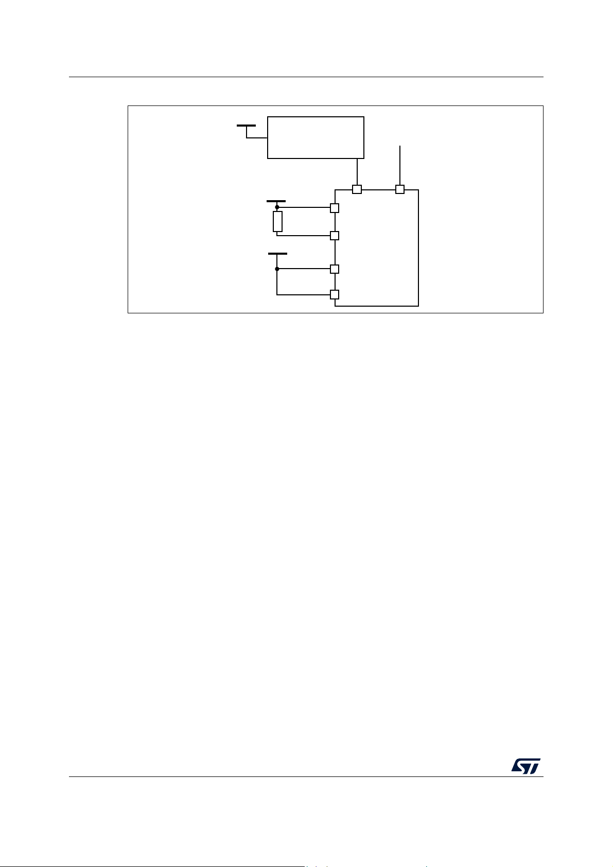
Functional overview STM32F722xx STM32F723xx
ai18498V3
BYPASS_REG
V
CAP_1
V
CAP_2
PA0
V12
V
DD
NRST
V
DD
Application reset
signal (optional)
External V
CAP_1/2
power
supply supervisor
Ext. reset controller active
when V
CAP_1/2
< Min V
12
V12
Figure 12. Regulator OFF
The following conditions must be respected:
• V
should always be higher than V
DD
CAP_1
and V
to avoid current injection
CAP_2
between power domains.
• If the time for V
V
to reach 1.7 V, then PA0 should be kept low to cover both conditions: until V
DD
and V
CAP_2
reach V
• Otherwise, if the time for V
than the time for V
and V
CAP_1
minimum value and until V
12
to reach 1.7 V, then PA0 could be asserted low externally (see
DD
CAP_2
CAP_1
to reach V
and V
CAP_2
minimum value is faster than the time for
12
reaches 1.7 V (see Figure 13).
DD
to reach V
minimum value is slower
12
CAP_1
Figure 14).
• If V
CAP_1
and V
CAP_2
go below V
minimum value and VDD is higher than 1.7 V, then a
12
reset must be asserted on PA0 pin.
Note: The minimum value of V
Note: On the LQFP64 pin package, the V
depends on the maximum frequency targeted in the application.
12
is not available.
CAP_2
34/230 DS11853 Rev 7
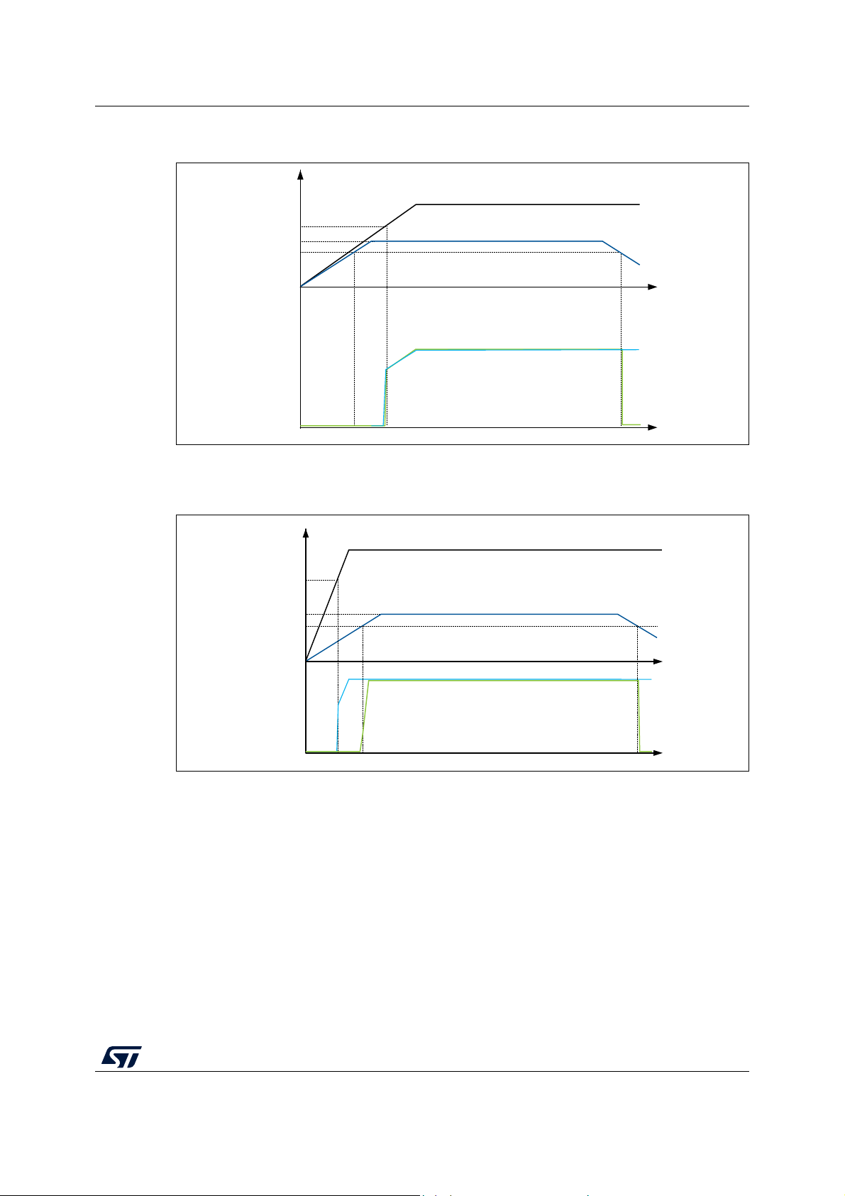
STM32F722xx STM32F723xx Functional overview
ai18491f
V
DD
time
Min V
12
PDR = 1.7 V or 1.8 V
V
CAP_1
/ V
CAP_2
V
12
NRST
time
V
DD
time
Min V
12
V
CAP_1
/ V
CAP_2
V
12
PA0 asserted externally
NRST
time
ai18492e
PDR = 1.7 V or 1.8 V
Figure 13. Startup in regulator OFF: slow VDD slope
- power-down reset risen after V
CAP_1/VCAP_2
1. This figure is valid whatever the internal reset mode (ON or OFF).
stabilization
Figure 14. Startup in regulator OFF mode: fast VDD slope
- power-down reset risen before V
CAP_1/VCAP_2
stabilization
1. This figure is valid whatever the internal reset mode (ON or OFF).
DS11853 Rev 7 35/230
49
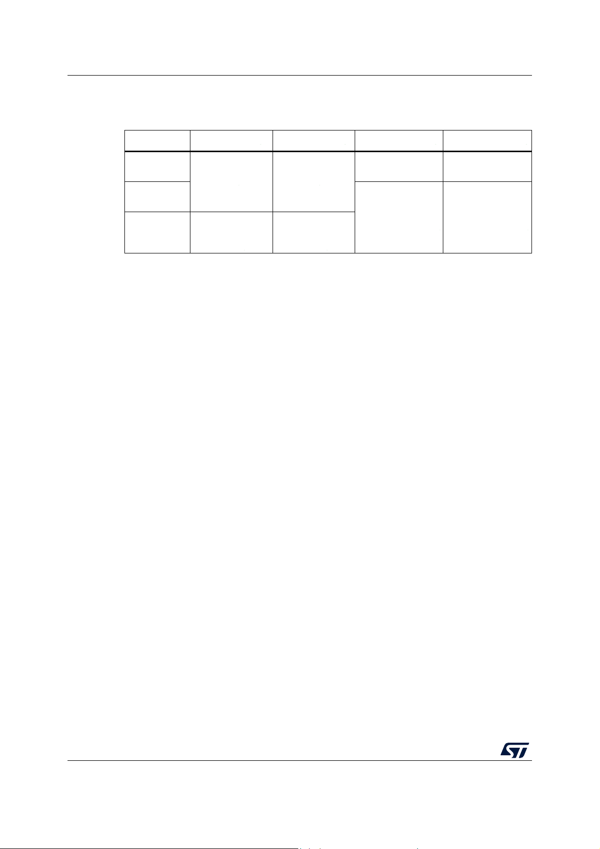
Functional overview STM32F722xx STM32F723xx
3.16.3 Regulator ON/OFF and internal reset ON/OFF availability
Package Regulator ON Regulator OFF Internal reset ON Internal reset OFF
LQFP64,
LQFP100
LQFP144
LQFP176,
UFBGA144,
UFBGA176
Table 4. Regulator ON/OFF and internal reset ON/OFF availability
Yes N o
Yes
Yes
BYPASS_REG set
to V
SS
BYPASS_REG set
No
Yes
to V
DD
Yes
PDR_ON set to V
PDR_ON set to V
DD
Yes
3.17 Real-time clock (RTC), backup SRAM and backup registers
The RTC is an independent BCD timer/counter. It supports the following features:
• Calendar with subsecond, seconds, minutes, hours (12 or 24 format), week day, date,
month, year, in BCD (binary-coded decimal) format.
• Automatic correction for 28, 29 (leap year), 30, and 31 days of the month.
• Two programmable alarms.
• On-the-fly correction from 1 to 32767 RTC clock pulses. This can be used to
synchronize it with a master clock.
• Reference clock detection: a more precise second source clock (50 or 60 Hz) can be
used to enhance the calendar precision.
• Digital calibration circuit with 0.95 ppm resolution, to compensate for quartz crystal
inaccuracy.
• Three anti-tamper detection pins with programmable filter.
• Timestamp feature which can be used to save the calendar content. This function can
be triggered by an event on the timestamp pin, or by a tamper event, or by a switch to
V
mode.
BAT
• 17-bit auto-reload wakeup timer (WUT) for periodic events with programmable
resolution and period.
SS
The RTC and the 32 backup registers are supplied through a switch that takes power either
from the V
supply when present or from the V
DD
The backup registers are 32-bit registers used to store 128 bytes of user application data
when V
DD power is not present. They are not reset by a system or power reset, or when the
device wakes up from Standby mode.
The RTC clock sources can be:
• A 32.768 kHz external crystal (LSE)
• An external resonator or oscillator(LSE)
• The internal low power RC oscillator (LSI, with typical frequency of 32 kHz)
• The high-speed external clock (HSE) divided by 32
The RTC is functional in V
mode and in all low-power modes when it is clocked by the
BAT
LSE. When clocked by the LSI, the RTC is not functional in V
all low-power modes.
36/230 DS11853 Rev 7
BAT
pin.
mode, but is functional in
BAT
STM32F722xx STM32F723xx Functional overview
All the RTC events (Alarm, WakeUp Timer, Timestamp or Tamper) can generate an interrupt
and wakeup the device from the low-power modes.
3.18 Low-power modes
The devices support three low-power modes to achieve the best compromise between low
power consumption, short startup time and available wakeup sources:
• Sleep mode
In Sleep mode, only the CPU is stopped. All peripherals continue to operate and can
wake up the CPU when an interrupt/event occurs.
• Stop mode
The Stop mode achieves the lowest power consumption while retaining the contents of
SRAM and registers. All clocks in the 1.2 V domain are stopped, the PLL, the HSI RC
and the HSE crystal oscillators are disabled.
The voltage regulator can be put either in main regulator mode (MR) or in low-power
mode (LPR). Both modes can be configured as follows (see Table 5: Voltage regulator
modes in stop mode):
– Normal mode (default mode when MR or LPR is enabled)
– Under-drive mode.
The device can be woken up from the Stop mode by any of the EXTI line (the EXTI line
source can be one of the 16 external lines, the PVD output, the RTC alarm / wakeup /
tamper / time stamp events, the USB OTG FS/HS wakeup and the LPTIM1
asynchronous interrupt).
Table 5. Voltage regulator modes in stop mode
Voltage regulator
configuration
Normal mode MR ON LPR ON
Under-drive mode MR in under-drive mode LPR in under-drive mode
Main regulator (MR) Low-power regulator (LPR)
• Standby mode
The Standby mode is used to achieve the lowest power consumption. The internal
voltage regulator is switched off so that the entire 1.2 V domain is powered off. The
PLL, the HSI RC and the HSE crystal oscillators are also switched off. After entering
Standby mode, the SRAM and register contents are lost except for registers in the
backup domain and the backup SRAM when selected.
The device exits the Standby mode when an external reset (NRST pin), an IWDG reset,
a rising or falling edge on one of the 6 WKUP pins (PA0, PA2, PC1, PC13, PI8, PI11),
or an RTC alarm / wakeup / tamper /time stamp event occurs.
The Standby mode is not supported when the embedded voltage regulator is bypassed
and the 1.2 V domain is controlled by an external power.
DS11853 Rev 7 37/230
49

Functional overview STM32F722xx STM32F723xx
3.19 V
The V
supercapacitor, or from V
operation
BAT
pin allows to power the device V
BAT
when no external battery and an external supercapacitor are
DD
present.
The V
The V
operation is activated when VDD is not present.
BAT
pin supplies the RTC, the backup registers and the backup SRAM.
BAT
Note: When the microcontroller is supplied from V
do not exit it from V
When the PDR_ON pin is connected to V
no more available and the V
operation.
BAT
pin should be connected to VDD.
BAT
SS
3.20 Timers and watchdogs
The devices include two advanced-control timers, eight general-purpose timers, two basic
timers and two watchdog timers.
All timer counters can be frozen in debug mode.
Tab le 6 compares the features of the advanced-control, general-purpose and basic timers.
domain from an external battery, an external
BAT
, external interrupts and RTC alarm/events
BAT
(Internal Reset OFF), the V
functionality is
BAT
38/230 DS11853 Rev 7

STM32F722xx STM32F723xx Functional overview
Timer
type
Advanced
-control
General
purpose
Timer
TIM1,
TIM8
TIM2,
TIM5
TIM3,
TIM4
Counter
resolution
16-bit
32-bit
16-bit
Counter
Down,
Up/down
Down,
Up/down
Down,
Up/down
TIM9 16-bit Up
TIM10,
TIM11
16-bit Up
Table 6. Timer feature comparison
type
Up,
Up,
Up,
Prescaler
factor
Any
integer
between 1
and 65536
Any
integer
between 1
and 65536
Any
integer
between 1
and 65536
Any
integer
between 1
and 65536
Any
integer
between 1
and 65536
DMA
request
generation
Yes 4 Yes 1 08 2 16
Yes 4 No 54 108/216
Yes 4 No 54 108/216
No 2 No 108 216
No 1 No 108 216
Capture/
compare
channels
Complem
entary
output
Max
interface
clock
(MHz)
Max
timer
clock
(MHz)
(1)
Any
TIM12 16-bit Up
integer
between 1
No 2 No 54 108/216
and 65536
Any
TIM13,
TIM14
16-bit Up
integer
between 1
No 1 No 54 108/216
and 65536
Any
Basic
TIM6,
TIM7
16-bit Up
integer
between 1
Yes 0 No 54 108/216
and 65536
1. The maximum timer clock is either 108 or 216 MHz depending on TIMPRE bit configuration in the RCC_DCKCFGR
register.
DS11853 Rev 7 39/230
49

Functional overview STM32F722xx STM32F723xx
3.20.1 Advanced-control timers (TIM1, TIM8)
The advanced-control timers (TIM1, TIM8) can be seen as three-phase PWM generators
multiplexed on 6 channels. They have complementary PWM outputs with programmable
inserted dead times. They can also be considered as complete general-purpose timers.
Their 4 independent channels can be used for:
• Input capture
• Output compare
• PWM generation (edge- or center-aligned modes)
• One-pulse mode output
If configured as standard 16-bit timers, they have the same features as the general-purpose
TIMx timers. If configured as 16-bit PWM generators, they have full modulation capability (0100%).
The advanced-control timer can work together with the TIMx timers via the Timer Link
feature for synchronization or event chaining.
The TIM1 and TIM8 support independent DMA request generation.
3.20.2 General-purpose timers (TIMx)
There are ten synchronizable general-purpose timers embedded in the STM32F722xx and
STM32F723xx devices (see Tabl e 6 for differences).
• TIM2, TIM3, TIM4, TIM5
The STM32F722xx and STM32F723xx include 4 full-featured general-purpose timers:
TIM2, TIM5, TIM3, and TIM4.The TIM2 and TIM5 timers are based on a 32-bit autoreload up/downcounter and a 16-bit prescaler. The TIM3 and TIM4 timers are based on
a 16-bit auto-reload up/downcounter and a 16-bit prescaler. They all feature 4
independent channels for input capture/output compare, PWM or one-pulse mode
output. This gives up to 16 input capture/output compare/PWMs on the largest
packages.
The TIM2, TIM3, TIM4, TIM5 general-purpose timers can work together, or with the
other general-purpose timers and the advanced-control timers TIM1 and TIM8 via the
Timer Link feature for synchronization or event chaining.
Any of these general-purpose timers can be used to generate PWM outputs.
TIM2, TIM3, TIM4, TIM5 all have independent DMA request generation. They are
capable of handling quadrature (incremental) encoder signals and the digital outputs
from 1 to 4 hall-effect sensors.
• TIM9, TIM10, TIM11, TIM12, TIM13, and TIM14
These timers are based on a 16-bit auto-reload upcounter and a 16-bit prescaler.
TIM10, TIM11, TIM13, and TIM14 feature one independent channel, whereas TIM9
and TIM12 have two independent channels for input capture/output compare, PWM or
one-pulse mode output. They can be synchronized with the TIM2, TIM3, TIM4, TIM5
full-featured general-purpose timers. They can also be used as simple time bases.
3.20.3 Basic timers TIM6 and TIM7
These timers are mainly used for the DAC trigger and waveform generation. They can also
be used as a generic 16-bit time base.
The TIM6 and TIM7 support independent DMA request generation.
40/230 DS11853 Rev 7

STM32F722xx STM32F723xx Functional overview
3.20.4 Low-power timer (LPTIM1)
The low-power timer has an independent clock and is running also in Stop mode if it is
clocked by LSE, LSI or an external clock. It is able to wakeup the devices from Stop mode.
This low-power timer supports the following features:
• 16-bit up counter with 16-bit autoreload register
• 16-bit compare register
• Configurable output: pulse, PWM
• Continuous / one-shot mode
• Selectable software / hardware input trigger
• Selectable clock source:
• Internal clock source: LSE, LSI, HSI or APB clock
• External clock source over LPTIM input (working even with no internal clock source
running, used by the Pulse Counter Application)
• Programmable digital glitch filter
• Encoder mode
3.20.5 Independent watchdog
The independent watchdog is based on a 12-bit downcounter and 8-bit prescaler. It is
clocked from an independent 32 kHz internal RC and as it operates independently from the
main clock, it can operate in Stop and Standby modes. It can be used either as a watchdog
to reset the device when a problem occurs, or as a free-running timer for application timeout
management. It is hardware- or software-configurable through the option bytes.
3.20.6 Window watchdog
The window watchdog is based on a 7-bit downcounter that can be set as free-running. It
can be used as a watchdog to reset the device when a problem occurs. It is clocked from
the main clock. It has an early warning interrupt capability and the counter can be frozen in
debug mode.
3.20.7 SysTick timer
This timer is dedicated to real-time operating systems, but could also be used as a standard
downcounter. It features:
• A 24-bit downcounter
• Autoreload capability
• Maskable system interrupt generation when the counter reaches 0
• Programmable clock source
DS11853 Rev 7 41/230
49

Functional overview STM32F722xx STM32F723xx
3.21 Inter-integrated circuit interface (I2C)
The devices embed 3 I2Cs. Refer to Table 7: I2C implementation for the features
implementation.
2
The I
C bus interface handles communications between the microcontroller and the serial
2
I
C bus. It controls all I2C bus-specific sequencing, protocol, arbitration and timing.
The I2C peripheral supports:
2
• I
C-bus specification and user manual rev. 5 compatibility:
– Slave and master modes, multimaster capability
– Standard-mode (Sm), with a bitrate up to 100 kbit/s
– Fast-mode (Fm), with a bitrate up to 400 kbit/s
– Fast-mode Plus (Fm+), with a bitrate up to 1 Mbit/s and 20 mA output drive I/Os
– 7-bit and 10-bit addressing mode, multiple 7-bit slave addresses
– Programmable setup and hold times
– Optional clock stretching
• System Management Bus (SMBus) specification rev 2.0 compatibility:
– Hardware PEC (Packet Error Checking) generation and verification with ACK
control
– Address resolution protocol (ARP) support
– SMBus alert
• Power System Management Protocol (PMBus
• Independent clock: a choice of independent clock sources allowing the I
communication speed to be independent from the PCLK reprogramming.
• Programmable analog and digital noise filters
• 1-byte buffer with DMA capability
Table 7. I2C implementation
I2C features
(1)
TM
) specification rev 1.1 compatibility
2
C
I2C1 I2C2 I2C3
Standard-mode (up to 100 kbit/s) X X X
Fast-mode (up to 400 kbit/s) X X X
Fast-mode Plus with 20 mA output drive I/Os (up to 1 Mbit/s) X X X
Programmable analog and digital noise filters X X X
SMBus/PMBus hardware support X X X
Independent clock X X X
1. X: supported.
42/230 DS11853 Rev 7

STM32F722xx STM32F723xx Functional overview
3.22 Universal synchronous/asynchronous receiver transmitters
(USART)
The devices embed USARTs. Refer to Table 8: USART implementation for the features
implementation.
The universal synchronous asynchronous receiver transmitter (USART) offers a flexible
means of full-duplex data exchange with external equipment requiring an industry standard
NRZ asynchronous serial data format.
The USART peripheral supports:
• Full-duplex asynchronous communications
• Configurable oversampling method by 16 or 8 to give flexibility between speed and
clock tolerance
• Dual clock domain allowing convenient baud rate programming independent from the
PCLK reprogramming
• A common programmable transmit and receive baud rate of up to 27 Mbit/s when
USART clock source is system clock frequency (max is 216 MHz) and oversampling by
8 is used.
• Auto baud rate detection
• Programmable data word length (7 or 8 or 9 bits) word length
• Programmable data order with MSB-first or LSB-first shifting
• Progarmmable parity (odd, even, no parity)
• Configurable stop bits (1 or 1.5 or 2 stop bits)
• Synchronous mode and clock output for synchronous communications
• Single-wire half-duplex communications
• Separate signal polarity control for transmission and reception
• Swappable Tx/Rx pin configuration
• Hardware flow control for modem and RS-485 transceiver
• Multiprocessor communications
• LIN master synchronous break send capability and LIN slave break detection capability
• IrDA SIR encoder decoder supporting 3/16 bit duration for normal mode
• Smartcard mode ( T=0 and T=1 asynchronous protocols for Smartcards as defined in
the ISO/IEC 7816-3 standard)
• Support for Modbus communication
Tab le 8 summarizes the implementation of all U(S)ARTs instances
Data Length 7, 8 and 9 bits
Hardware flow control for modem X X
Continuous communication using DMA X X
Multiprocessor communication X X
Synchronous mode X -
Table 8. USART implementation
features
(1)
DS11853 Rev 7 43/230
USART1/2/3/6 UART4/5/7/8
49

Functional overview STM32F722xx STM32F723xx
Table 8. USART implementation (continued)
features
Smartcard mode X -
Single-wire half-duplex communication X X
IrDA SIR ENDEC block X X
LIN mode X X
Dual clock domain X X
Receiver timeout interrupt X X
Modbus communication X X
Auto baud rate detection X X
Driver Enable X X
1. X: supported.
(1)
USART1/2/3/6 UART4/5/7/8
3.23 Serial peripheral interface (SPI)/inter- integrated sound
interfaces (I
2
S)
The devices feature up to five SPIs in slave and master modes in full-duplex and simplex
communication modes. SPI1, SPI4, and SPI5 can communicate at up to 50 Mbit/s, SPI2
and SPI3 can communicate at up to 25 Mbit/s. The 3-bit prescaler gives 8 master mode
frequencies and the frame is configurable from 4 to 16 bits. The SPI interfaces support the
NSS pulse mode, TI mode and Hardware CRC calculation. All the SPIs can be served by
the DMA controller.
Three standard I
2
S interfaces (multiplexed with SPI1, SPI2 and SPI3) are available. They
can be operated in master or slave mode, in simplex communication modes, and can be
configured to operate with a 16-/32-bit resolution as an input or output channel. Audio
sampling frequencies from 8 kHz up to 192 kHz are supported. When either or both of the
2
I
S interfaces is/are configured in master mode, the master clock can be output to the
external DAC/CODEC at 256 times the sampling frequency.
2
All I
Sx can be served by the DMA controller.
3.24 Serial audio interface (SAI)
The devices embed two serial audio interfaces.
The serial audio interface is based on two independent audio subblocks which can operate
as transmitter or receiver with their FIFO. Many audio protocols are supported by each
block: I
supporting audio sampling frequencies from 8 kHz up to 192 kHz. Both subblocks can be
configured in master or in slave mode.
2
S standards, LSB or MSB-justified, PCM/DSP, TDM, AC’97 and SPDIF output,
In master mode, the master clock can be output to the external DAC/CODEC at 256 times of
the sampling frequency.
The two sub-blocks can be configured in synchronous mode when full-duplex mode is
required.
44/230 DS11853 Rev 7

STM32F722xx STM32F723xx Functional overview
SAI1 and SAI2 can be served by the DMA controller
3.25 Audio PLL (PLLI2S)
The devices feature an additional dedicated PLL for audio I2S and SAI applications. It allows
to achieve an error-free I
performance, while using USB peripherals.
The PLLI2S configuration can be modified to manage an I
without disabling the main PLL (PLL) used for CPU and USB interfaces.
The audio PLL can be programmed with very low error to obtain sampling rates ranging
from 8 KHz to 192 KHz.
In addition to the audio PLL, a master clock input pin can be used to synchronize the
2
I
S/SAI flow with an external PLL (or Codec output).
2
S sampling clock accuracy without compromising on the CPU
2
S/SAI sample rate change
3.26 Audio PLL (PLLSAI)
An additional PLL dedicated to audio is used for the SAI1 peripheral in case the PLLI2S is
programmed to achieve another audio sampling frequency (49.152 MHz or 11.2896 MHz)
and the audio application requires both sampling frequencies simultaneously.
3.27 SD/SDIO/MMC card host interface (SDMMC)
SDMMC host interfaces are available, that support MultiMediaCard System Specification
Version 4.2 in three different databus modes: 1-bit (default), 4-bit and 8-bit.
The interface allows data transfer at up to 50 MHz, and is compliant with the SD Memory
Card Specification Version 2.0.
The SDMMC Card Specification Version 2.0 is also supported with two different databus
modes: 1-bit (default) and 4-bit.
The current version supports only one SD/SDMMC/MMC4.2 card at any one time and a
stack of MMC4.1 or previous.
The SDMMC can be served by the DMA controller
3.28 Controller area network (bxCAN)
The CAN is compliant with the 2.0A and B (active) specifications with a bit rate up to 1
Mbit/s. It can receive and transmit standard frames with 11-bit identifiers as well as
extended frames with 29-bit identifiers. The CAN has three transmit mailboxes, two receive
FIFOs with 3 stages and 28 shared scalable filter banks (all of them can be used even if one
CAN is used). 256 bytes of SRAM are allocated to the CAN.
DS11853 Rev 7 45/230
49

Functional overview STM32F722xx STM32F723xx
3.29 Universal serial bus on-the-go full-speed (OTG_FS)
The devices embed an USB OTG full-speed device/host/OTG peripheral with integrated
transceivers. The USB OTG FS peripheral is compliant with the USB 2.0 specification and
with the OTG 2.0 specification. It has software-configurable endpoint setting and supports
suspend/resume. The USB OTG controller requires a dedicated 48 MHz clock that is
generated by a PLL connected to the HSE oscillator.
The major features are:
• Combined Rx and Tx FIFO size of 1.28 Kbytes with dynamic FIFO sizing
• Supports the session request protocol (SRP) and host negotiation protocol (HNP)
• 1 bidirectional control endpoint + 5 IN endpoints + 5 OUT endpoints
• 12 host channels with periodic OUT support
• Software configurable to OTG1.3 and OTG2.0 modes of operation
• USB 2.0 LPM (Link Power Management) support
• Internal FS OTG PHY support
• HNP/SNP/IP inside (no need for any external resistor)
• BCD support
For the OTG/Host modes, a power switch is needed in case bus-powered devices are
connected
3.30 Universal serial bus on-the-go high-speed (OTG_HS)
The devices embed an USB OTG high-speed (up to 480 Mbit/s) device/host/OTG
peripheral. The USB OTG HS supports both full-speed and high-speed operations. It
integrates the transceivers for full-speed operation (12 Mbit/s).
The STM32F722xx devices feature a UTMI low-pin interface (ULPI) for high-speed
operation (480 Mbit/s). When using the USB OTG HS in HS mode, an external PHY device
connected to the ULPI is required.
The STM32F723xx devices feature an integrated PHY HS.
The USB OTG HS peripheral is compliant with the USB 2.0 specification and with the OTG
2.0 specification. It has a software-configurable endpoint setting and supports
suspend/resume. The USB OTG controller requires a dedicated 48 MHz clock that is
generated by a PLL connected to the HSE oscillator.
The major features are:
• Combined Rx and Tx FIFO size of 4 Kbytes with dynamic FIFO sizing
• Supports the session request protocol (SRP) and host negotiation protocol (HNP)
• 8 bidirectional endpoints
• 16 host channels with periodic OUT support
• Software configurable to OTG1.3 and OTG2.0 modes of operation
• USB 2.0 LPM (Link Power Management) support
• For the STM32F722xx devices: External HS or HS OTG operation supporting ULPI in
SDR mode. The OTG PHY is connected to the microcontroller ULPI port through 12
signals. It can be clocked using the 60 MHz output.
• For the STM32F723xx devices: Internal HS OTG PHY support.
46/230 DS11853 Rev 7

STM32F722xx STM32F723xx Functional overview
• Internal USB DMA
• HNP/SNP/IP inside (no need for any external resistor)
• For OTG/Host modes, a power switch is needed in case bus-powered devices are
connected
Universal Serial Bus controller on-the-go High-Speed PHY controller
(USBPHYC) only on STM32F723xx devices.
The USB HS PHY controller:
– Sets the PHYPLL1/2 values for the PHY HS
– Sets the other controls on the PHY HS
– Controls and monitors the USB PHY’s LDO
3.31 Random number generator (RNG)
All the devices embed an RNG that delivers 32-bit random numbers generated by an
integrated analog circuit.
3.32 General-purpose input/outputs (GPIOs)
Each of the GPIO pins can be configured by software as output (push-pull or open-drain,
with or without pull-up or pull-down), as input (floating, with or without pull-up or pull-down)
or as peripheral alternate function. Most of the GPIO pins are shared with digital or analog
alternate functions. All GPIOs are high-current-capable and have speed selection to better
manage internal noise, power consumption and electromagnetic emission.
The I/O configuration can be locked if needed by following a specific sequence in order to
avoid spurious writing to the I/Os registers.
A Fast I/O handling allows a maximum I/O toggling up to 108 MHz.
3.33 Analog-to-digital converters (ADCs)
Three 12-bit analog-to-digital converters are embedded and each ADC shares up to 16
external channels, performing conversions in the single-shot or scan mode. In the scan
mode, an automatic conversion is performed on a selected group of analog inputs.
Additional logic functions embedded in the ADC interface allow:
• Simultaneous sample and hold
• Interleaved sample and hold
The ADC can be served by the DMA controller. An analog watchdog feature allows very
precise monitoring of the converted voltage of one, some or all selected channels. An
interrupt is generated when the converted voltage is outside the programmed thresholds.
To synchronize A/D conversion and timers, the ADCs could be triggered by any of TIM1,
TIM2, TIM3, TIM4, TIM5, or TIM8 timer.
DS11853 Rev 7 47/230
49

Functional overview STM32F722xx STM32F723xx
3.34 Temperature sensor
The temperature sensor has to generate a voltage that varies linearly with the temperature.
The conversion range is between 1.7 V and 3.6 V. The temperature sensor is internally
connected to the same input channel as V
sensor output voltage into a digital value. When the temperature sensor and V
conversion are enabled at the same time, only V
As the offset of the temperature sensor varies from chip to chip due to process variation, the
internal temperature sensor is mainly suitable for applications that detect temperature
changes instead of absolute temperatures. If an accurate temperature reading is needed,
then an external temperature sensor part should be used.
, ADC1_IN18, which is used to convert the
BAT
conversion is performed.
BAT
BAT
3.35 Digital-to-analog converter (DAC)
The two 12-bit buffered DAC channels can be used to convert two digital signals into two
analog voltage signal outputs.
This dual digital Interface supports the following features:
• Two DAC converters: one for each output channel
• 8-bit or 12-bit monotonic output
• Left or right data alignment in 12-bit mode
• Synchronized update capability
• Noise-wave generation
• Triangular-wave generation
• Dual DAC channel independent or simultaneous conversions
• DMA capability for each channel
• External triggers for conversion
• Input voltage reference V
Eight DAC trigger inputs are used in the device. The DAC channels are triggered through
the timer update outputs that are also connected to different DMA streams.
REF+
3.36 Serial wire JTAG debug port (SWJ-DP)
The Arm SWJ-DP interface is embedded, and is a combined JTAG and serial wire debug
port that enables either a serial wire debug or a JTAG probe to be connected to the target.
The debug is performed using 2 pins only instead of 5 required by the JTAG (JTAG pins
could be re-used as GPIO with alternate function): the JTAG TMS and TCK pins are shared
with SWDIO and SWCLK, respectively, and a specific sequence on the TMS pin is used to
switch between JTAG-DP and SW-DP.
48/230 DS11853 Rev 7

STM32F722xx STM32F723xx Functional overview
3.37 Embedded Trace Macrocell™
The Arm Embedded Trace Macrocell provides a greater visibility of the instruction and data
flow inside the CPU core by streaming compressed data at a very high rate from the
STM32F722xx and STM32F723xx device through a small number of ETM pins to an
external hardware trace port analyzer (TPA) device. The TPA is connected to a host
computer using the USB or any other high-speed channel. The real-time instruction and
data flow activity can be recorded and then formatted for display on the host computer that
runs the debugger software. The TPA hardware is commercially available from common
development tool vendors.
The Embedded Trace Macrocell operates with third party debugger software tools.
DS11853 Rev 7 49/230
49
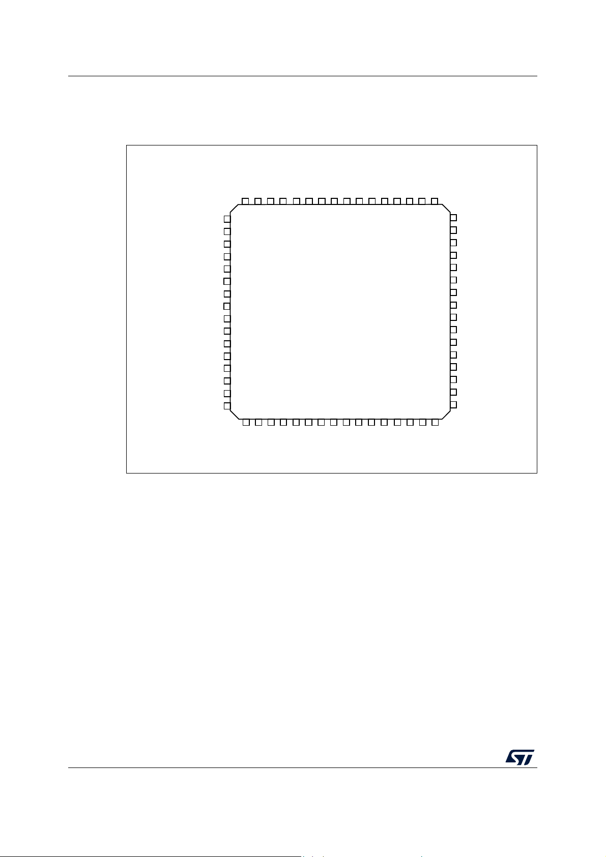
Pinouts and pin description STM32F722xx STM32F723xx
64 63 62 61 60 59 58 57 56 55 54 53 52 51 50 49
48
47
46
45
44
43
42
41
40
39
38
37
36
35
34
33
17 18 19 20 21 22 23 24 29 30 31 3225 26 27 28
1
2
3
4
5
6
7
8
9
10
11
12
13
14
15
16
VBAT
PC14-OSC32_IN
PC15-OSC32_OUT
NRST
PC0
PC1
PC2
PC3
VSSA
VDDA
PA0-WKUP
PA1
PA2
VDD
PD2
PC12
PC11
PC10
VDD
VSS
PC8
PC7
PC6
PB12
VSS
PA3
VDD
PC4
PB2
PB10
PH1-OSC_OUT
PH0-OSC_IN
PC13
VSS
PB11
VSS
VDD
LQFP64
MS40455V3
PA13
PA12
PA11
PA10
PA9
PA8
PC9
PB15
PB14
PB13
PA4
PA5
PA6
PA7
PB0
PB1
PB9
PB8
BOOT0
PB7
PB6
PB5
PB4
PB3
PA15
PA14
VCAP_1
4 Pinouts and pin description
Figure 15. STM32F722xx LQFP64 pinout
50/230 DS11853 Rev 7
1. The above figure shows the package top view.
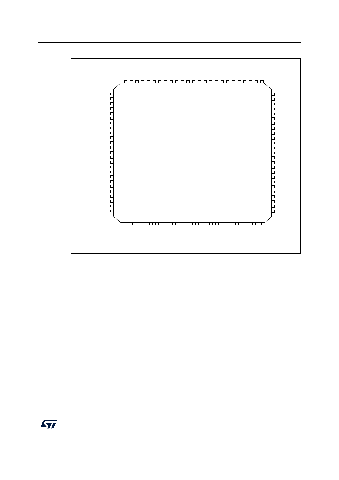
STM32F722xx STM32F723xx Pinouts and pin description
100999897969594939291908988878685848382818079787776
1
2
3
4
5
6
7
8
9
10
11
12
13
14
15
16
17
18
19
20
21
22
23
24
25
75
74
73
72
71
70
69
68
67
66
65
64
63
62
61
60
59
58
57
56
55
54
53
52
51
PE2
PE3
PE4
PE5
PE6
PC14-OSC32_IN
PC15-OSC32_OUT
VSS
VDD
PH0-OSC_IN
PC0
PC1
PC2
PC3
VSSA
VREF+
VDDA
VDD
VSS
VCAP_2
PC9
PC8
PC7
PC6
VSS
VDD
PA4
PB1
PB2
PE7
PE8
PE9
VCAP_1
VDD
VDD
VSS
PD7
PD6
PD5
PD4
PD3
PD2
PD1
PD0
PC12
PC11
PC10
26272829303132333435363738394041424344454647484950
MSv40457V1
LQFP100
PC13
PH1-OSC_OUT
PA0-WKUP
PA1
PA2
PA3
PA5
PA6
PA7
PC4
PB0
PC5
PE13
PE14
PE15
PB10
PB11
PE10
PE12
PE11
VSS
PD12
PD11
PD8
PB15
PB14
PB13
PB12
PD9
PD10
PD13
PD14
PD15
PA9
PA8
PA10
PA11
PA12
PA13
PA15
PA14
PE1
PE0
PB9
PB8
BOOT0
PB7
PB6
PB5
PB4
PB3
VBAT
NRST
Figure 16. STM32F722xx LQFP100 pinout
1. The above figure shows the package top view.
DS11853 Rev 7 51/230
99
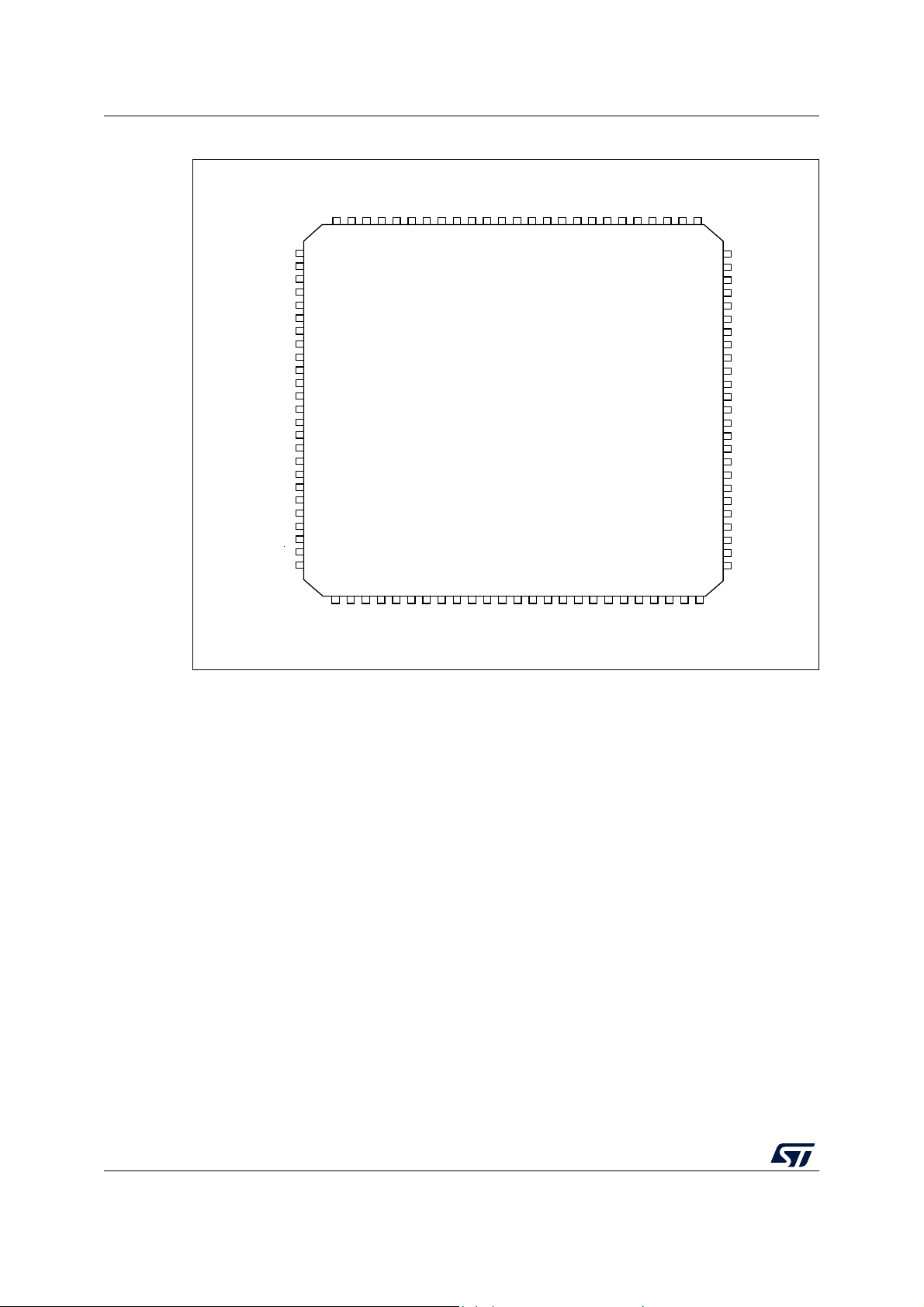
Pinouts and pin description STM32F722xx STM32F723xx
100999897969594939291908988878685848382818079787776
1
2
3
4
5
6
7
8
9
10
11
12
13
14
15
16
17
18
19
20
21
22
23
24
25
75
74
73
72
71
70
69
68
67
66
65
64
63
62
61
60
59
58
57
56
55
54
53
52
51
PE2
PE3
PE4
PE5
PE6
PC14-OSC32_IN
PC15-OSC32_OUT
VSS
VDD
PH0-OSC_IN
PC0
PC1
PC2
PC3
VSSA
VREF+
VDDA
VDD
VSS
VCAP_2
PC9
PC8
PC7
PC6
VSS
VDD
PA4
PB1
PB2
PE7
PE8
PE9
VCAP_1
VDD
VDD
VSS
PD7
PD6
PD5
PD4
PD3
PD2
PD1
PD0
PC12
PC11
PC10
26272829303132333435363738394041424344454647484950
MSv63474V1
LQFP100
PC13
PH1-OSC_OUT
PA0-WKUP
PA1
PA2
PA3
PA5
PA6
PA7
PC4
PB0
PC5
PE13
PE14
PE15
PB10
PB11
PE10
PE12
PE11
VSS
PD12
PD11
VDD12OTGHS
VDDPHYHS
OTG_HS_REXT
PB13
PB12
PB14
PB15
PD13
PD14
PD15
PA9
PA8
PA10
PA11
PA12
PA13
PA15
PA14
PE1
PE0
PB9
PB8
BOOT0
PB7
PB6
PB5
PB4
PB3
VBAT
NRST
Figure 17. STM32F723xx LQFP100 pinout
1. The above figure shows the package top view.
52/230 DS11853 Rev 7

STM32F722xx STM32F723xx Pinouts and pin description
MSv42002V2
A
B
C
D
E
F
G
H
J
K
PC3
PA4
PA3
VDD
PA7
7
BOOT0
PB4
PB5
PB6
PE0
PB0
PB1
PE8
PE7
PE9
5
PD5
PD0
PC11
PC12
PD2
PA5
PA6
PC4
PC5
PB2
6
PB3
PD4
PD3
PD6
PD7
PE15
PE11
PE12
PE13
PE14
4
PD1
PA15
PA14
PC7
PE10
PC10
PD13
PD11
PB10
PB11
VCAP_1
VSS
3
VCAP_2
PA9
PA8
PD12
OTG_HS
_REXT
PB13
PB12
VDD
2
VSS
PA12
PA10
PC8
PD15
PD14
VDD12
OTGHS
PB15
PB14
VDD
USB
1
VDD
PA13
PA11
PC9
PC6
PA0
PA1
VSS
PC0
8
VSS
PB7
PB8
PB9
PE5
VDD
PH0
PH1
PC2
VSSA
10
PE3
PE6
VBAT
PC13
PC15
PE2
PE4
PC14
NRST
PC1
VREF+
VDDA
VSS
9
VDD
PE1
PA2
Figure 18. STM32F723xx WLCSP100 ballout (with OTG PHY HS)
1. The above figure shows the package top view.
DS11853 Rev 7 53/230
99
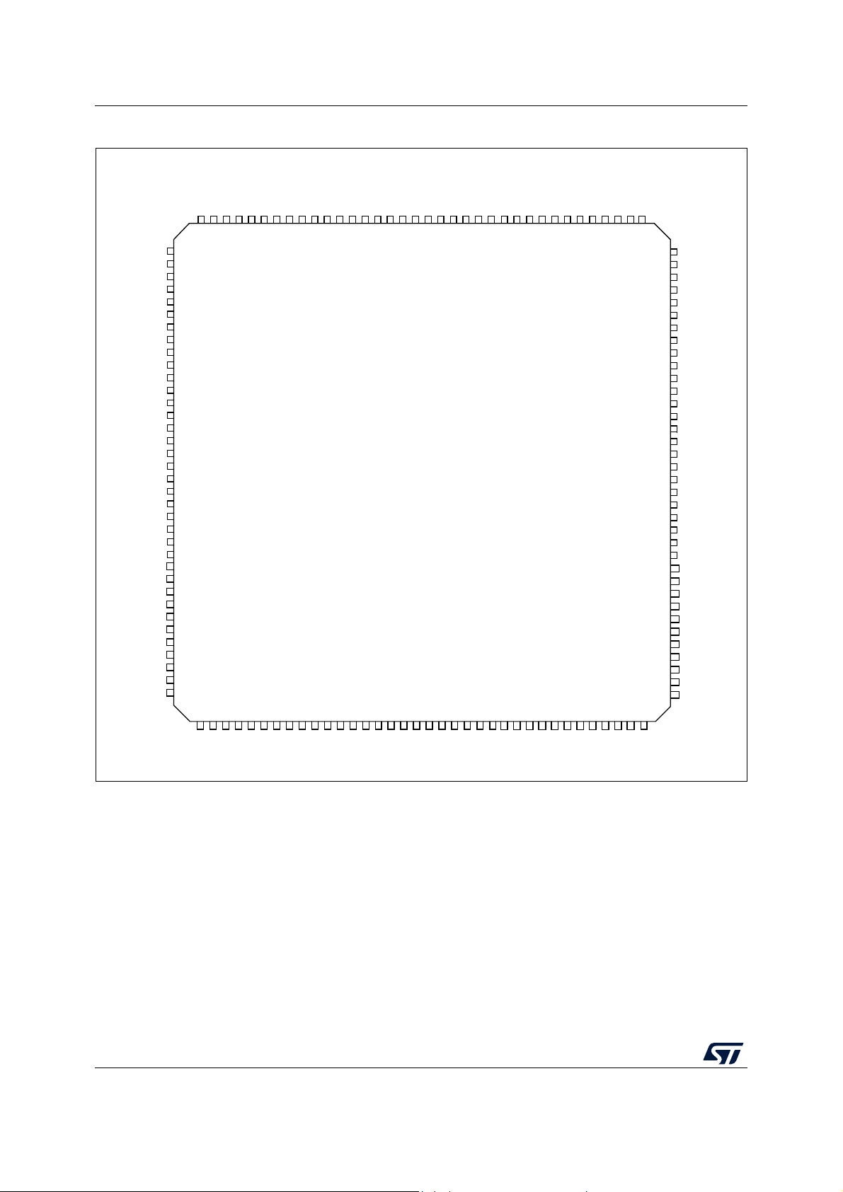
Pinouts and pin description STM32F722xx STM32F723xx
VDDPDR_ON
PE1
PE0
PB9
PB8
BOOT0
PB7
PB6
PB5
PB4
PB3
PG15
VDDVSSPG14
PG13
PG12
PG11
PG10
PG9
PD7
PD6
V
DDSDMMC
VSSPD5
PD4
PD3
PD2
PD1
PD0
PC12
PC11
PC10
PA 15
PA 14
PE2
V
DD
PE3
V
SS
PE4
PE5
PA 13
PE6
PA 12
VBAT
PA 11
PC13
PA 10
PC14
PA 9
PC15
PA 8
PF0
PC9
PF1
PC8
PF2
PC7
PF3
PC6
PF4
V
DDUSB
PF5
V
SS
V
SS
PG8
V
DD
PG7
PF6
PG6
PF7
PG5
PF8
PG4
PF9
PG3
PF10
PG2
PH0
PD15
PH1
PD14
NRST
V
DD
PC0
V
SS
PC1
PD13
PC2
PD12
PC3
PD11
V
SSA
PD10
V
DD
PD9
V
REF+
PD8
V
DDA
PB15
PA 0
PB14
PA 1
PB13
PA 2
PB12
PA 3
V
SS
V
DD
PA 4
PA 5
PA 6
PA 7
PC4
PC5
PB0
PB1
PB2
PF11
PF12
V
DD
PF13
PF14
PF15
PG0
PG1
PE7
PE8
PE9
V
SS
V
DD
PE10
PE11
PE12
PE13
PE14
PE15
PB10
PB11
V
DD
144
143
142
141
140
139
138
137
136
135
134
133
132
131
130
129
128
127
126
125
124
123
122
121
109
1
2
3
4
5
6
7
8
9
10
11
12
13
14
15
16
17
18
19
20
21
22
23
24
25
108
107
106
105
104
103
102
101
100
99
98
97
96
95
94
93
92
91
90
89
88
87
86
85
84
3738394041424344454647484950515253545556575859
60
72
LQFP144
120
119
118
117
116
115
114
113
112
111
110
6162636465666768697071
26
27
28
29
30
31
32
33
34
35
36
83
82
81
80
79
78
77
76
75
74
73
V
CAP_2
V
SS
MS39132V1
V
CAP_1
Figure 19. STM32F722xx LQFP144 pinout
1. The above figure shows the package top view.
54/230 DS11853 Rev 7
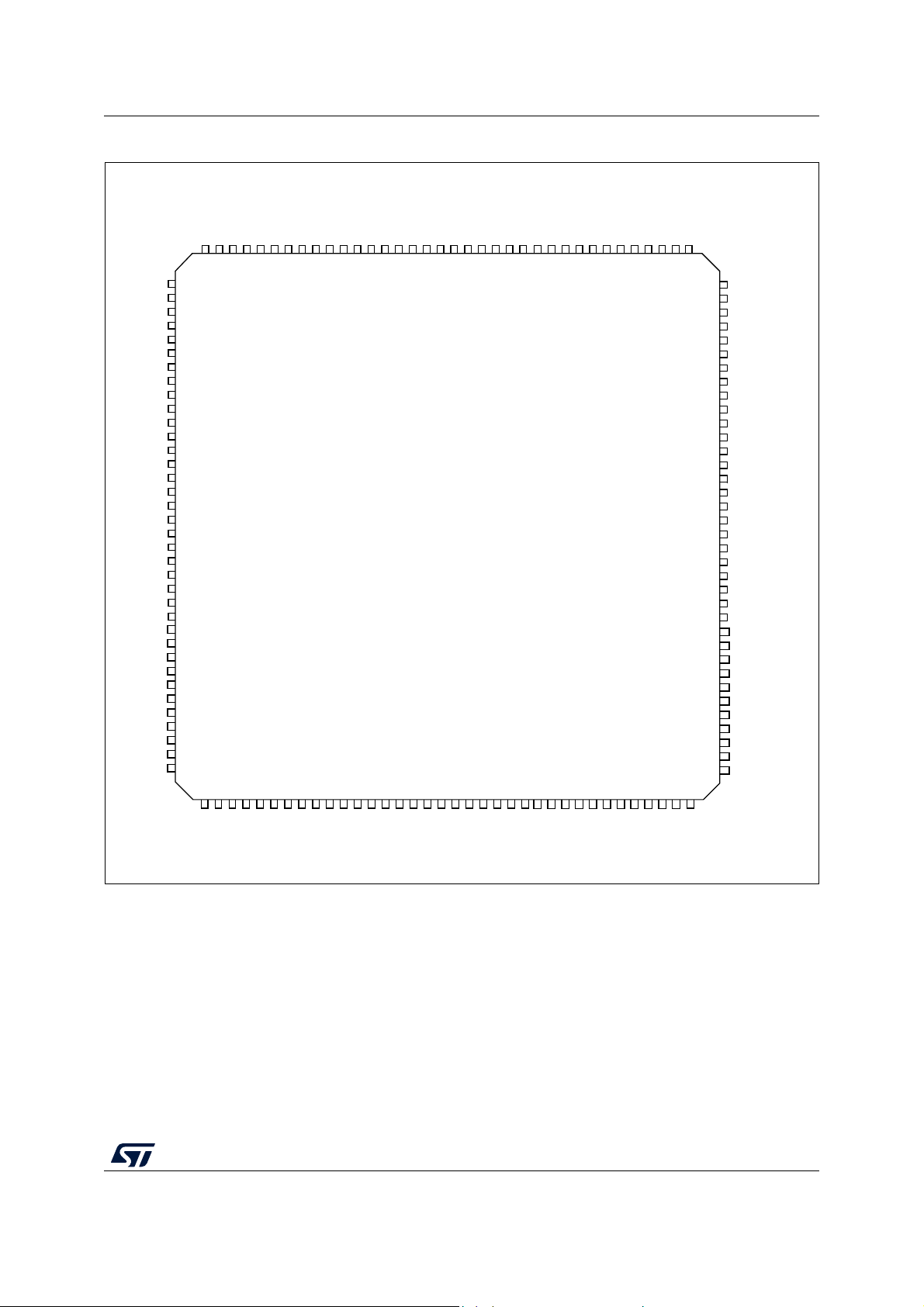
STM32F722xx STM32F723xx Pinouts and pin description
VDDPDR_ON
PE1
PE0
PB9
PB8
BOOT0
PB7
PB6
PB5
PB4
PB3
PG15
VDDVSSPG14
PG13
PG12
PG11
PG10
PG9
PD7
PD6
V
DDSDMMC
VSSPD5
PD4
PD3
PD2
PD1
PD0
PC12
PC11
PC10
PA 15
PA 14
PE2
V
DD
PE3
V
SS
PE4
PE5
PA13
PE6
PA12
VBAT
PA11
PC13
PA10
PC14
PA 9
PC15
PA 8
PF0
PC9
PF1
PC8
PF2
PC7
PF3
PC6
PF4
V
DDUSB
PF5
V
SS
V
SS
PG8
V
DD
PG5
PF6
PG4
PF7
PG3
PF8
PG2
PF9
PD15
PF10
PD14
PH0
PH1
NRST
V
DD
PC0
V
SS
PC1
PD13
PC2
PD12
PC3
PD11
V
SSA
PD10
V
DD
V
REF+
V
DDA
PB15
PA 0
PB14
PA 1
PB13
PA 2
PB12
PA 3
V
SS
V
DD
PA 4
PA 5
PA 6
PA 7
PC4
PC5
PB0
PB1
PB2
PF11
PF12
V
DD
PF13
PF14
PF15
PG0
PG1
PE7
PE8
PE9
V
SS
V
DD
PE10
PE11
PE12
PE13
PE14
PE15
PB10
PB11
V
DD
144
143
142
141
140
139
138
137
136
135
134
133
132
131
130
129
128
127
126
125
124
123
122
121
109
1
2
3
4
5
6
7
8
9
10
11
12
13
14
15
16
17
18
19
20
21
22
23
24
25
108
107
106
105
104
103
102
101
100
99
98
97
96
95
94
93
92
91
90
89
88
87
86
85
84
3738394041424344454647484950515253545556575859
60
72
LQFP144
with HS PHY
120
119
118
117
116
115
114
113
112
111
110
6162636465666768697071
26
27
28
29
30
31
32
33
34
35
36
83
82
81
80
79
78
77
76
75
74
73
V
CAP_2
V
SS
MS41014V1
V
CAP_1
PD9
PD8
VDD12OTGHS
OTG_HS_REXT
Figure 20. STM32F723xx LQFP144 pinout
1. The above figure shows the package top view.
DS11853 Rev 7 55/230
99
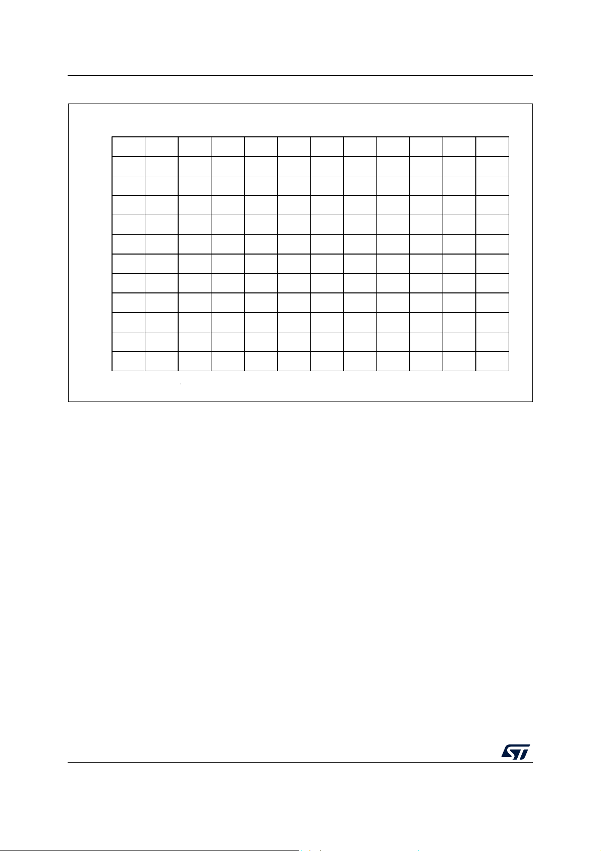
Pinouts and pin description STM32F722xx STM32F723xx
MSv42000V1
PC13 PE3 PE2 PE1 PE0 PB4 PB3 PD6 PD7 PA15 PA14 PA13
123456789101112
A
B
C
D
E
F
G
H
J
K
L
M
PC14-
OSC32_IN
PE4 PE5 PE6 PB9 PB5 PG15 PG12 PD5 PC11 PC10 PA12
PC15-
OSC32_OUT
VBAT PF0 PF1 PB8 PG11 PD4 PC12 VDDUSB PA 11
PH0 -
OSC_IN
VSS VDD PD1 PA10 PA 9
PH1 -
OSC_OUT
PF3 PF4 PD0 PC9 PA8
NRST PF7 PC8 PC7
PF10 PF9 PG8 PC6
PC0 PC1 PC2
VDD12OTG
HS
OTG_HS
_REXT
PG5
VSSA PA0 PA4 PG4 PG3 PG2
VREF- PA1 PA5 PC5 PF13 PE13 PD9 PD13 PD14 PD15
VREF+ PA2 PA6 PB0 PF12 PF15 PE8 PE14 PD8 PD12 PB14 PB15
VDDA PA 3 PA7 PB1 PF11 PF14 PE7 PE15 PB10 PB11 PB12 PB13
PF2 BOOT0 PB7 PG13
PB6 PG14
PG10 PD3
PG9 PD2VSS VSSPF5 PDR_ON
PF6 VDDVDD VDDVDD VDDVDD VDD
PF8 VSSVSS VCAP_2VDD VDDVSS VDD
PE11 PD11VSS VCAP_1PC3
BYPASS_
REG
PE12 PD10PG1 PE10PC4 PB2
PG0 PE9
Figure 21. STM32F723xx UFBGA144 ballout (with OTG PHY HS)
1. The above figure shows the package top view.
56/230 DS11853 Rev 7

STM32F722xx STM32F723xx Pinouts and pin description
MS41015V1
PDR_ON
V
DD
PE1
PE0
PB9
PB8
BOOT0
PB7
PB6
PB5
PB4
PB3
PG15
VDDVSSPG14
PG13
PG12
PG11
PG10
PG9
PD7
PD6
V
DDSDMMCVSS
PD5
PD4
PD3
PD2
PD1
PD0
PC12
PC11
PC10
PI7
PI6
PE2
V
DD
PE3
V
SS
PE4
PE5
PA13
PE6
PA12
VBAT
PA11
PI8
PA10
PC14
PA9
PC15
PA8
PF0
PC9
PF1
PC8
PF2
PC7
PF3
PC6
PF4
V
DDUSB
PF5
V
SS
PG8
PG7
PF6
PG6
PF7
PG5
PF8
PG4
PF9
PG3
PF10
PG2
PH0
PD15
PH1
PD14
NRST
V
DD
PC0
V
SS
PC1
PD13
PC2
PD12
PC3
PD11
PD10
PD9
VREF+
PD8
PB15
PA0
PB14
PA1
PB13
PA2
PB12
PA3
BYPASS_REG
V
DD
PA4
PA5
PA6
PA7
PC4
PC5
PB0
PB1
PB2
PF11
PF12
VSS
V
DD
PF13
PF14
PF15
PG0
PG1
PE7
PE8
PE9
V
SS
V
DD
PE10
PE11
PE12
PE13
PE14
PE15
PB10
PB11
V
CAP_1
V
DD
176
175
174
173
172
171
170
169
168
167
166
165
164
163
162
161
160
159
158
157
156
155
154
153
141
1
2
3
4
5
6
7
8
9
10
11
12
13
14
15
16
17
18
19
20
21
22
23
24
25
132
131
130
129
128
127
126
125
124
123
122
121
120
119
118
117
116
115
114
113
112
111
110
109
108
4546474849505152535455565758596061626364656667
68
80
LQFP176
152
151
150
149
148
147
146
145
144
143
142
6970717273747576777879
26
27
28
29
30
31
32
33
34
35
36
107
106
105
104
103
102
101
100
99
98
89
V
CAP_2
PI4
PA15
PA14
VDDVSSPI3
PI2
PI5
140
139
138
137
136
135
134
133
PH4
PH5
PH6
PH7
PH8
PH9
PH10
PH11
88
81828384858687
PI1
PI0
PH15
PH14
PH13
V
DD
V
SS
PH12
96
95
94
93
92
91
90
97
37
38
39
40
41
42
43
44
PC13
PI9
PI10
PI11
VSS
PH2
PH3
VDD
VSS
VDD
VDD
VSSA
VDDA
Figure 22. STM32F722xx LQFP176 pinout
1. The above figure shows the package top view.
DS11853 Rev 7 57/230
99

Pinouts and pin description STM32F722xx STM32F723xx
MS41082V1
PDR_ON
V
DD
PE1
PE0
PB9
PB8
BOOT0
PB7
PB6
PB5
PB4
PB3
PG15
VDDVSSPG14
PG13
PG12
PG11
PG10
PG9
PD7
PD6
V
DDSDMMCVSS
PD5
PD4
PD3
PD2
PD1
PD0
PC12
PC11
PC10
PI7
PI6
PE2
V
DD
PE3
V
SS
PE4
PE5
PA13
PE6
PA12
VBAT
PA11
PI8
PA10
PC14
PA9
PC15
PA8
PF0
PC9
PF1
PC8
PF2
PC7
PF3
PC6
PF4
V
DDUSB
PF5
V
SS
PG8
PF6
PF7
PG5
PF8
PG4
PF9
PG3
PF10
PG2
PH0
PD15
PH1
PD14
NRST
V
DD
PC0
V
SS
PC1
PD11
PC2
PD10
PC3
PD9
PD8
PB15
VREF+
PB14
VDD12OTGHS
PA0
OTG_HS_REXT
PA1
PB13
PA2
PB12
PA3
BYPASS_REG
V
DD
PA4
PA5
PA6
PA7
PC4
PC5
PB0
PB1
PB2
PF11
PF12
VSS
V
DD
PF13
PF14
PF15
PG0
PG1
PE7
PE8
PE9
V
SS
V
DD
PE10
PE11
PE12
PE13
PE14
PE15
PB10
PB11
V
CAP_1
V
DD
176
175
174
173
172
171
170
169
168
167
166
165
164
163
162
161
160
159
158
157
156
155
154
153
141
1
2
3
4
5
6
7
8
9
10
11
12
13
14
15
16
17
18
19
20
21
22
23
24
25
132
131
130
129
128
127
126
125
124
123
122
121
120
119
118
117
116
115
114
113
112
111
110
109
108
4546474849505152535455565758596061626364656667
68
80
LQFP176
with HS PHY
152
151
150
149
148
147
146
145
144
143
142
6970717273747576777879
26
27
28
29
30
31
32
33
34
35
36
107
106
105
104
103
102
101
100
99
98
89
V
CAP_2
PI4
PA15
PA14
VDDVSSPI3
PI2
PI5
140
139
138
137
136
135
134
133
PH4
PH5
PH6
PH7
PH8
PH9
PH10
PH11
88
81828384858687
PI1
PI0
PH15
PH14
PH13
V
DD
V
SS
PH12
96
95
94
93
92
91
90
97
37
38
39
40
41
42
43
44
PC13
PI9
PI10
PI11
VSS
PH2
PH3
VDD
VSS
VDD
VDD
VSSA
VDDA
PD12
PD13
Figure 23. STM32F723xx LQFP176 pinout
1. The above figure shows the package top view.
58/230 DS11853 Rev 7

STM32F722xx STM32F723xx Pinouts and pin description
MS39130V1
1 2 3 9 10 11 12 13 14 15
APE3PE2
PE1 PE0 PB8
PB5
PG14 PG13 PB4 PB3 PD7 PC12 P A15 PA1 4 PA13
BPE4PE5
PE6
PB9 PB7
PB6
PG15 PG12 PG11 PG10 PD6 PD0 PC11 PC10 P A12
C
VBAT
PI7 PI6 PI5
PDR_ON
VDD
VDD
VDD
SDMMC
VDD PG9 PD5 PD1 PI3 PI2 PA11
D
PC13 PI8
PI9 PI4 BOOT0
VSS VSS VSS PD4 PD3 PD2 PH15 P I1 PA10
E
PC14
PF0 PI10
PI11
PH13 PH14 P I0 PA9
FPC15
VSS
VDD
PH2
VSS
VSS VSS VSS VS S VSS VCAP2 PC9 PA8
G
PH0 VSS VDD PH3
VSS
VSS VSS VSS VSS VSS VDD PC8 PC7
H
PH1
PF2
PF1
PH4 VSS
VSS VSS VSS VSS VSS VDDUSB PG8 PC6
J
NRST PF3 PH5 VSS
VSS VSS VSS VS S VDD VD D PG7 PG6
K
PF7
PF6
PF4
VDD
VSS
VSS VSS VSS VSS PH12 PG5 PG4 PG3
L
PF10
PF9
PF5
BYPASS_
REG
PH11 PH10 PD15 PG2
MVSSAPC0
PF8
PC1 PC2 PC3
PB2
PG1 VSS VSS VCAP_1 PH6 PH8 PH9 PD14 PD13
NVREF-
PA0
PA4
PC4
PF13
PG0 VDD VDD VDD PE13 PH7 PD12 PD11 PD10
PVREF+
PA2 PA6 PA5
PC5
PF12
PF15 PE8 PE9 PE11 PE14 PB12 PB13 PD9 PD8
R VDDA PA3 PA7 PB1
PB0
PF11
PF14 PE7 PE10 PE12 PE15 PB10 PB11 PB14 PB15
VSS
45678
PA1
Figure 24. STM32F723xx UFBGA176 ballout
1. The above figure shows the package top view.
DS11853 Rev 7 59/230
99

Pinouts and pin description STM32F722xx STM32F723xx
Figure 25. STM32F723xx UFBGA176 ballout (with OTG PHY HS)
1 2 3 9 10 11 12 13 14 15
APE3PE2
BPE4PE5
PI7 PI6 PI5
VBAT
C
PC13 PI8
D
PF0 PI10
PC14
E
FPC15
G
H
J
K
L
MVSSAPC0
NVREF-
VSS
PH0 VSS VDD PH3
PF2
PH1
NRST PF3 PH5 VSS
PF6
PF7
PF9
PF10
PA1
45678
PE1 PE0 PB8
PB9 PB7
PE6
PI9 PI4 BOOT0
PI11
PH2
VDD
PF1
PH4 VSS
PF4
PF5
VDD
BYPASS_
PF8
REG
PC1 PC2 PC3
PA4
PA0
VDD
VSS
PC4
PB5
PB6
PDR_ON
VSS
VSS
VSS
PB2
PF13
PG14 PG13 PB4 PB3 PD7 PC12 P A15 PA1 4 PA13
PG15 PG12 PG11 PG10 PD6 PD0 PC11 PC10 P A12
VDD
VDD
VSS VSS VSS PD4 PD3 PD2 PH15 P I1 PA10
VSS VSS VSS VS S VSS VCAP2 PC9 PA8
VSS VSS VSS VSS VSS VDD PC8 PC7
VSS VSS VSS VSS VSS VDDUSB PG8 PC6
VSS VSS VSS VS S VDD VD D
VSS VSS VSS VSS PH12 PG5 PG4 PG3
PG1 VSS VSS VCAP_1 PH6 PH8 PH9 PD14 PD13
PG0 VDD VDD VDD PE13 PH7 PD12 PD11 PD10
VDD PG9 PD5 PD1 PI3 PI2 PA11
SDMMC
PH13 PH14 P I0 PA9
PH11 PH10 PD15 PG2
VDD12
OTGHS
OTG_HS
_REXT
PVREF+
R VDDA PA3 PA7 PB1
PA2 PA6 PA5
PC5
PB0
1. The above figure shows the package top view.
PF12
PF15 PE8 PE9 PE11 PE14 PB12 PB13 PD9 PD8
PF14 PE7 PE10 PE12 PE15 PB10 PB11 PB14 PB15
PF11
MS42001V1
60/230 DS11853 Rev 7

STM32F722xx STM32F723xx Pinouts and pin description
Table 9. Legend/abbreviations used in the pinout table
Name Abbreviation Definition
Pin name
Unless otherwise specified in brackets below the pin name, the pin function during and after
reset is the same as the actual pin name
S Supply pin
Pin type
I Input only pin
I/O Input / output pin
FT 5 V tolerant I/O
FTf 5V tolerant I/O, I2C Fm+ option.
I/O structure
TTa 3.3 V tolerant I/O directly connected to ADC
B Dedicated BOOT pin
RST Bidirectional reset pin with weak pull-up resistor
Notes Unless otherwise specified by a note, all I/Os are set as floating inputs during and after reset
Alternate
functions
Additional
functions
Functions selected through GPIOx_AFR registers
Functions directly selected/enabled through peripheral registers
DS11853 Rev 7 61/230
99

62/230 DS11853 Rev 7
Table 10. STM32F722xx and STM32F723xx pin and ball definition
Pin Number
STM32F722xx STM32F723xx
Pinouts and pin description STM32F722xx STM32F723xx
Pin name
(function after
reset)
(1)
Pin type
I/O structure
LQFP64
LQFP100
LQFP144
UFBGA176
LQFP176
LQFP100
WLCSP100
UFBGA176
UFBGA144
LQFP144
LQFP176
- 1 1 A2 1 1 C9 A2 A3 1 1 PE2 I/O FT -
- 2 2 A1 2 2 A10 A1 A2 2 2 PE3 I/O FT -
- 3 3 B1 3 3 D9 B1 B2 3 3 PE4 I/O FT -
- 4 4 B2 4 4 E8 B2 B3 4 4 PE5 I/O FT -
Notes
Alternate functions
TRACECLK, SPI4_SCK,
SAI1_MCLK_A,
QUADSPI_BK1_IO2, FMC_A23,
EVENTOUT
TRACED0, SAI1_SD_B,
FMC_A19, EVENTOUT
TRACED1, SPI4_NSS,
SAI1_FS_A, FMC_A20,
EVENTOUT
TRACED2, TIM9_CH1,
SPI4_MISO, SAI1_SCK_A,
FMC_A21, EVENTOUT
Additional
functions
-
-
-
-
TRACED3, TIM1_BKIN2,
- 5 5 B3 5 5 B10 B3 B4 5 5 PE6 I/O FT -
TIM9_CH2, SPI4_MOSI,
SAI1_SD_A, SAI2_MCK_B,
FMC_A22, EVENTOUT
1 6 6 C1 6 6 C10 C1 C2 6 6 VBAT S - - - -
-

Table 10. STM32F722xx and STM32F723xx pin and ball definition (continued)
Pin Number
STM32F722xx STM32F723xx
STM32F722xx STM32F723xx Pinouts and pin description
DS11853 Rev 7 63/230
Pin name
(function after
reset)
(1)
Pin type
I/O structure
LQFP64
LQFP100
LQFP144
UFBGA176
LQFP176
LQFP100
WLCSP100
UFBGA176
UFBGA144
LQFP144
LQFP176
- - - D2 7 - - D2 - - 7 PI8 I/O FT
2 7 7 D1 8 7 D10 D1 A1 7 8 PC13 I/O FT
PC14-
388E19 8 E9E1B18 9
OSC32_IN(PC14)I/O FT
PC15-
499F1109E10F1C1910
OSC32_OUT(P
I/O FT
C15)
- - - D3 11 - - D3 - - 11 PI9 I/O FT -
Notes
(2)
(3)
(2)
(3)
(2)
(3)
(5)
(2)
(3)
(5)
Alternate functions
EVENTOUT
EVENTOUT
EVENTOUT OSC32_IN
EVENTOUT OSC32_OUT
UART4_RX, CAN1_RX,
FMC_D30, EVENTOUT
Additional
functions
RTC_TAMP2/
RTC_TS,
WKUP5
RTC_TAMP1/
RTC_TS/
RTC_OUT,
WKUP4
-
- - - E3 12 - - E3 - - 12 PI10 I/O FT - FMC_D31, EVENTOUT -
---E413- -E4- -13 PI11 I/OFT
(4)
OTG_HS_ULPI_DIR,
EVENTOUT
WKUP6
- - - F2 14 - - F2 - - 14 VSS S - - - -
---F315- -F3- -15 VDD S-- - -
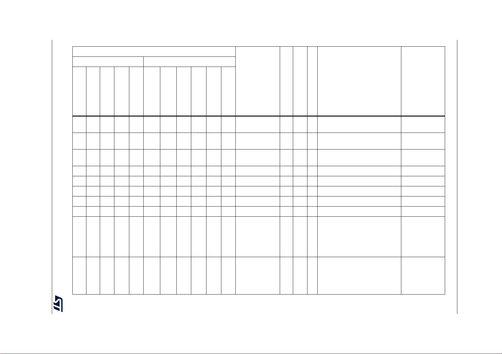
64/230 DS11853 Rev 7
Table 10. STM32F722xx and STM32F723xx pin and ball definition (continued)
Pin Number
STM32F722xx STM32F723xx
Pinouts and pin description STM32F722xx STM32F723xx
Pin name
(function after
LQFP64
LQFP100
LQFP144
UFBGA176
LQFP176
LQFP100
WLCSP100
UFBGA176
UFBGA144
LQFP144
LQFP176
- - 10 E2 16 - - E2 C3 10 16 PF0 I/O FTf -
- - 11 H3 17 - - H3 C4 11 17 PF1 I/O FTf -
- - 12 H2 18 - - H2 D4 12 18 PF2 I/O FT -
- - 13 J2 19 - - J2 E2 13 19 PF3 I/O FT - FMC_A3, EVENTOUT ADC3_IN9
- - 14 J3 20 - - J3 E3 14 20 PF4 I/O FT - FMC_A4, EVENTOUT ADC3_IN14
- - 15 K3 21 - - K3 E4 15 21 PF5 I/O FT - FMC_A5, EVENTOUT ADC3_IN15
- 1016G222 10 F9G2D21622 VSS S - - - -
- 11 17 G3 23 11 F10 G3 D3 17 23 VDD S - - - -
- - 18 K2 24 - - K2 F3 18 24 PF6 I/O FT -
reset)
(1)
Pin type
Notes
I/O structure
Alternate functions
I2C2_SDA, FMC_A0,
EVENTOUT
I2C2_SCL, FMC_A1,
EVENTOUT
I2C2_SMBA, FMC_A2,
EVENTOUT
TIM10_CH1, SPI5_NSS,
SAI1_SD_B, UART7_RX,
QUADSPI_BK1_IO3,
EVENTOUT
Additional
functions
-
-
-
ADC3_IN4
- - 19 K1 25 - - K1 F2 19 25 PF7 I/O FT -
TIM11_CH1, SPI5_SCK,
SAI1_MCLK_B, UART7_TX,
QUADSPI_BK1_IO2,
EVENTOUT
ADC3_IN5

Table 10. STM32F722xx and STM32F723xx pin and ball definition (continued)
Pin Number
STM32F722xx STM32F723xx
STM32F722xx STM32F723xx Pinouts and pin description
DS11853 Rev 7 65/230
Pin name
(function after
reset)
(1)
Pin type
Alternate functions
Notes
Additional
functions
I/O structure
LQFP64
LQFP100
LQFP144
UFBGA176
LQFP176
LQFP100
WLCSP100
UFBGA176
UFBGA144
LQFP144
LQFP176
SPI5_MISO, SAI1_SCK_B,
- - 20 L3 26 - - L3 G3 20 26 PF8 I/O FT -
UART7_RTS, TIM13_CH1,
QUADSPI_BK1_IO0,
ADC3_IN6
EVENTOUT
SPI5_MOSI, SAI1_FS_B,
- - 21 L2 27 - - L2 G2 21 27 PF9 I/O FT -
UART7_CTS, TIM14_CH1,
QUADSPI_BK1_IO1,
ADC3_IN7
EVENTOUT
- - 22 L1 28 - - L1 G1 22 28 PF10 I/O FT - EVENTOUT ADC3_IN8
5 12 23 G1 29 12 G10 G1 D1 23 29 PH0-OSC_IN I/O FT
6 13 24 H1 30 13 H10 H1 E1 24 30 PH1-OSC_OUT I/O FT
71425J131 14 G9J1F12531 NRST I/O
RS
T
8 1526M232 15 F8M2H12632 PC0 I/OFT
(5)
(5)
-- -
(4)
FMC_SDNWE, EVENTOUT
EVENTOUT OSC_IN
EVENTOUT OSC_OUT
SAI2_FS_B,
OTG_HS_ULPI_STP,
ADC1_IN10,
ADC2_IN10,
ADC3_IN10
9 1627M333 16 H9M3H22733 PC1 I/OFT-
TRACED0,
SPI2_MOSI/I2S2_SD,
SAI1_SD_A, EVENTOUT
ADC1_IN11,
ADC2_IN11,
ADC3_IN11,
RTC_TAMP3,
WKUP3
66/230 DS11853 Rev 7
Table 10. STM32F722xx and STM32F723xx pin and ball definition (continued)
Pin Number
STM32F722xx STM32F723xx
Pinouts and pin description STM32F722xx STM32F723xx
Pin name
(function after
reset)
(1)
Pin type
Alternate functions
Notes
Additional
functions
I/O structure
LQFP64
LQFP100
LQFP144
UFBGA176
LQFP176
LQFP100
WLCSP100
UFBGA176
UFBGA144
LQFP144
LQFP176
10 17 28 M4 34 17 J10 M4 H3 28 34 PC2 I/O FT
11 18 29 M5 35 18 F7 M5 H4 29 35 PC3 I/O FT
(4)
SPI2_MISO,
OTG_HS_ULPI_DIR,
FMC_SDNE0, EVENTOUT
(4)
SPI2_MOSI/I2S2_SD,
OTG_HS_ULPI_NXT,
FMC_SDCKE0, EVENTOUT
ADC1_IN12,
ADC2_IN12,
ADC3_IN12
ADC1_IN13,
ADC2_IN13,
ADC3_IN13
- - 30 - 36 - J7 - F10 30 36 VDD S - - - -
12 19 31 M1 37 19 K10 M1 J1 31 37 VSSA S - - - -
- - - N1 - - - N1 K1 - - VREF- S - - - -
13 20 32 P1 38 20 J9 P1 L1 32 38 VREF+ S - - - -
-2133R13921 K9R1M13339 VDDA S -- - -
14 22 34 N3 40 22 G8 N3 J2 34 40 PA0-WKUP I/O FT
TIM2_CH1/TIM2_ETR,
(5)
TIM5_CH1, TIM8_ETR,
USART2_CTS, UART4_TX,
SAI2_SD_B, EVENTOUT
ADC1_IN0,
ADC2_IN0,
ADC3_IN0,
WKUP1
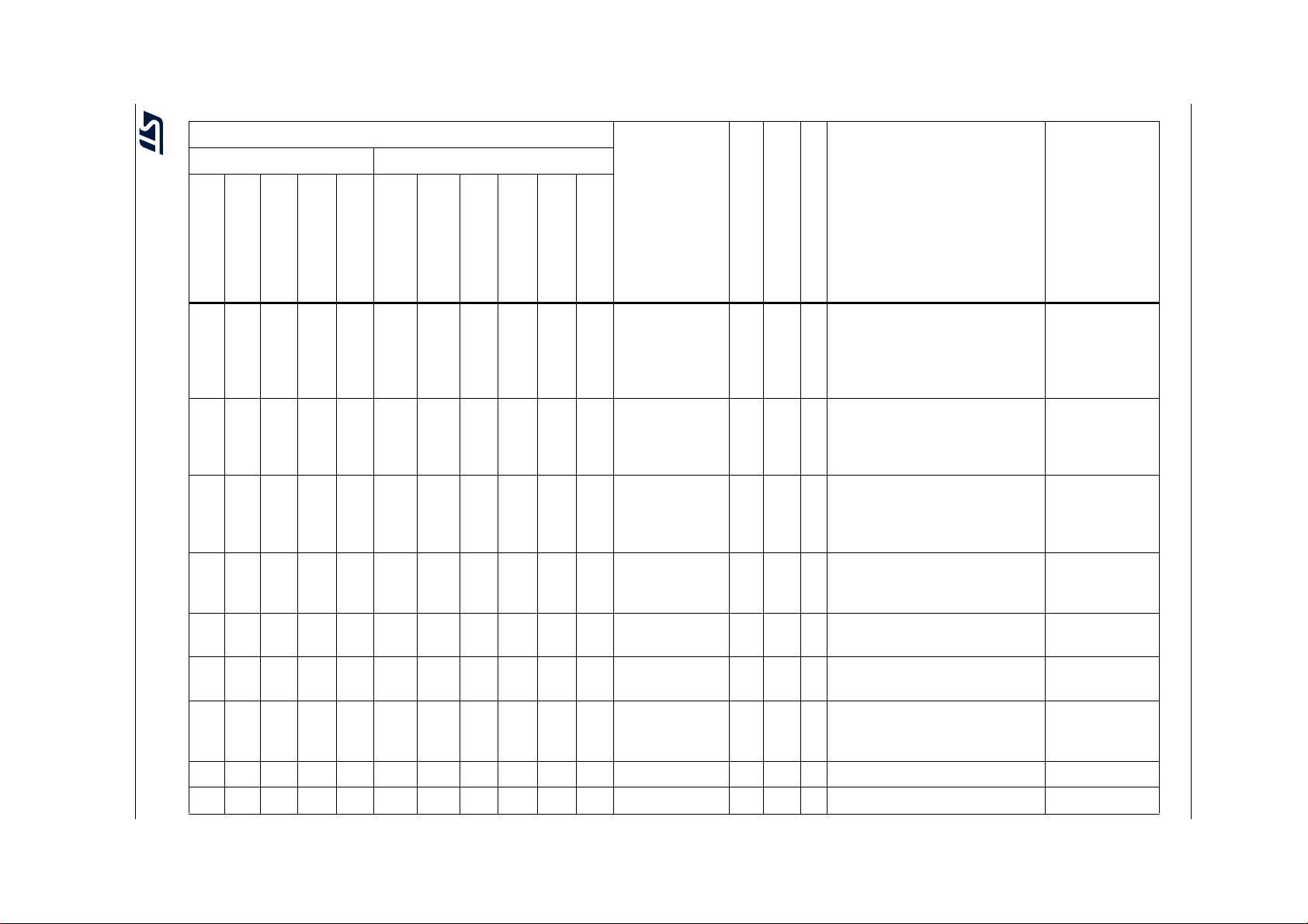
Table 10. STM32F722xx and STM32F723xx pin and ball definition (continued)
Pin Number
STM32F722xx STM32F723xx
STM32F722xx STM32F723xx Pinouts and pin description
DS11853 Rev 7 67/230
Pin name
(function after
reset)
(1)
Pin type
Notes
I/O structure
LQFP64
LQFP100
LQFP144
UFBGA176
LQFP176
LQFP100
WLCSP100
UFBGA176
UFBGA144
LQFP144
LQFP176
15 23 35 N2 41 23 J8 N2 K2 35 41 PA1 I/O FT -
16 24 36 P2 42 24 H8 P2 L2 36 42 PA2 I/O FT -
---F443- -F4- -43 PH2 I/OFT-
---G444- -G4- -44 PH3 I/OFT-
---H445- -H4- -45 PH4 I/OFTf
(4)
Alternate functions
TIM2_CH2, TIM5_CH2,
USART2_RTS, UART4_RX,
QUADSPI_BK1_IO3,
SAI2_MCK_B, EVENTOUT
TIM2_CH3, TIM5_CH3,
TIM9_CH1, USART2_TX,
SAI2_SCK_B, EVENTOUT
LPTIM1_IN2,
QUADSPI_BK2_IO0,
SAI2_SCK_B, FMC_SDCKE0,
EVENTOUT
QUADSPI_BK2_IO1,
SAI2_MCK_B, FMC_SDNE0,
EVENTOUT
I2C2_SCL, OTG_HS_ULPI_NXT,
EVENTOUT
Additional
functions
ADC1_IN1,
ADC2_IN1,
ADC3_IN1
ADC1_IN2,
ADC2_IN2,
ADC3_IN2,
WKUP2
-
-
-
---J446- -J4- -46 PH5 I/OFTf-
17 25 37 R2 47 25 H7 R2 M2 37 47 PA3 I/O FT
(4)
I2C2_SDA, SPI5_NSS,
FMC_SDNWE, EVENTOUT
TIM2_CH4, TIM5_CH4,
TIM9_CH2, USART2_RX,
OTG_HS_ULPI_D0, EVENTOUT
ADC1_IN3,
ADC2_IN3,
ADC3_IN3
18 26 38 - - 26 K8 - G4 38 - VSS S - - - -
- - - L4 48 - - L4 H5 - 48 BYPASS_REG I FT - - -
-
68/230 DS11853 Rev 7
Table 10. STM32F722xx and STM32F723xx pin and ball definition (continued)
Pin Number
STM32F722xx STM32F723xx
Pinouts and pin description STM32F722xx STM32F723xx
Pin name
(function after
reset)
(1)
Pin type
Alternate functions
Notes
Additional
functions
I/O structure
LQFP64
LQFP100
LQFP144
UFBGA176
LQFP176
LQFP100
WLCSP100
UFBGA176
UFBGA144
LQFP144
LQFP176
19 27 39 K4 49 27 - K4 F4 39 49 VDD S - - - -
20 28 40 N4 50 28 G7 N4 J3 40 50 PA4 I/O TTa -
21 29 41 P4 51 29 F6 P4 K3 41 51 PA5 I/O TTa
22 30 42 P3 52 30 G6 P3 L3 42 52 PA6 I/O FT -
SPI1_NSS/I2S1_WS,
SPI3_NSS/I2S3_WS,
USART2_CK, OTG_HS_SOF,
EVENTOUT
TIM2_CH1/TIM2_ETR,
(4)
TIM8_CH1N,
SPI1_SCK/I2S1_CK,
OTG_HS_ULPI_CK, EVENTOUT
TIM1_BKIN, TIM3_CH1,
TIM8_BKIN, SPI1_MISO,
TIM13_CH1, EVENTOUT
ADC1_IN4,
ADC2_IN4,
DAC_OUT1
ADC1_IN5,
ADC2_IN5,
DAC_OUT2
ADC1_IN6,
ADC2_IN6
TIM1_CH1N, TIM3_CH2,
23 31 43 R3 53 31 K7 R3 M3 43 53 PA7 I/O FT -
TIM8_CH1N,
SPI1_MOSI/I2S1_SD,
TIM14_CH1, FMC_SDNWE,
ADC1_IN7,
ADC2_IN7
EVENTOUT
24 32 44 N5 54 32 H6 N5 J4 44 54 PC4 I/O FT -
I2S1_MCK, FMC_SDNE0,
EVENTOUT
- 33 45 P5 55 33 J6 P5 K4 45 55 PC5 I/O FT - FMC_SDCKE0, EVENTOUT
ADC1_IN14,
ADC2_IN14
ADC1_IN15,
ADC2_IN15

Table 10. STM32F722xx and STM32F723xx pin and ball definition (continued)
Pin Number
STM32F722xx STM32F723xx
STM32F722xx STM32F723xx Pinouts and pin description
DS11853 Rev 7 69/230
Pin name
(function after
reset)
(1)
Pin type
Alternate functions
Notes
Additional
functions
I/O structure
LQFP64
LQFP100
LQFP144
UFBGA176
LQFP176
LQFP100
WLCSP100
UFBGA176
UFBGA144
LQFP144
LQFP176
25 34 46 R5 56 34 F5 R5 L4 46 56 PB0 I/O FT
26 35 47 R4 57 35 G5 R4 M4 47 57 PB1 I/O FT
(4)
TIM1_CH2N, TIM3_CH3,
TIM8_CH2N, UART4_CTS,
OTG_HS_ULPI_D1, EVENTOUT
(4)
TIM1_CH3N, TIM3_CH4,
TIM8_CH3N,
OTG_HS_ULPI_D2, EVENTOUT
ADC1_IN8,
ADC2_IN8
ADC1_IN9,
ADC2_IN9
SAI1_SD_A,
27 36 48 M6 58 36 K6 M6 J5 48 58 PB2 I/O FT -
SPI3_MOSI/I2S3_SD,
QUADSPI_CLK, EVENTOUT
- - 49 R6 59 - - R6 M5 49 59 PF11 I/O FT -
SPI5_MOSI, SAI2_SD_B,
FMC_SDNRAS, EVENTOUT
- - 50 P6 60 - - P6 L5 50 60 PF12 I/O FT - FMC_A6, EVENTOUT -
- - 51 M8 61 - - M8 - 51 61 VSS S - - - -
- - 52 N8 62 - - N8 G5 52 62 VDD S - - - -
-
-
- - 53 N6 63 - - N6 K5 53 63 PF13 I/O FT - FMC_A7, EVENTOUT -
- - 54 R7 64 - - R7 M6 54 64 PF14 I/O FT - FMC_A8, EVENTOUT -
- - 55 P7 65 - - P7 L6 55 65 PF15 I/O FT - FMC_A9, EVENTOUT -
- - 56 N7 66 - - N7 K6 56 66 PG0 I/O FT - FMC_A10, EVENTOUT -
- - 57 M7 67 - - M7 J6 57 67 PG1 I/O FT - FMC_A11, EVENTOUT -
70/230 DS11853 Rev 7
Table 10. STM32F722xx and STM32F723xx pin and ball definition (continued)
Pin Number
STM32F722xx STM32F723xx
Pinouts and pin description STM32F722xx STM32F723xx
Pin name
(function after
LQFP64
LQFP100
LQFP144
UFBGA176
LQFP176
LQFP100
WLCSP100
UFBGA176
UFBGA144
LQFP144
LQFP176
- 37 58 R8 68 37 J5 R8 M7 58 68 PE7 I/O FT -
- 3859P869 38 H5P8L75969 PE8 I/OFT-
- 3960P970 39 K5 P9K76070 PE9 I/OFT-
- - 61 M9 71 - - M9 H6 61 71 VSS S - - - -
- - 62 N9 72 - - N9 G6 62 72 VDD S - - - -
- 40 63 R9 73 40 E4 R9 J7 63 73 PE10 I/O FT -
- 41 64 P10 74 41 G4 P10 H8 64 74 PE11 I/O FT -
reset)
(1)
Pin type
Notes
I/O structure
Alternate functions
TIM1_ETR, UART7_Rx,
QUADSPI_BK2_IO0, FMC_D4,
EVENTOUT
TIM1_CH1N, UART7_Tx,
QUADSPI_BK2_IO1, FMC_D5,
EVENTOUT
TIM1_CH1, UART7_RTS,
QUADSPI_BK2_IO2, FMC_D6,
EVENTOUT
TIM1_CH2N, UART7_CTS,
QUADSPI_BK2_IO3, FMC_D7,
EVENTOUT
TIM1_CH2, SPI4_NSS,
SAI2_SD_B, FMC_D8,
EVENTOUT
Additional
functions
-
-
-
-
-
- 42 65 R10 75 42 H4 R10 J8 65 75 PE12 I/O FT -
- 43 66 N11 76 43 J4 N11 K8 66 76 PE13 I/O FT -
TIM1_CH3N, SPI4_SCK,
SAI2_SCK_B, FMC_D9,
EVENTOUT
TIM1_CH3, SPI4_MISO,
SAI2_FS_B, FMC_D10,
EVENTOUT
-
-
Table 10. STM32F722xx and STM32F723xx pin and ball definition (continued)
Pin Number
STM32F722xx STM32F723xx
STM32F722xx STM32F723xx Pinouts and pin description
DS11853 Rev 7 71/230
Pin name
(function after
reset)
(1)
Pin type
Alternate functions
Notes
Additional
functions
I/O structure
LQFP64
LQFP100
LQFP144
UFBGA176
LQFP176
LQFP100
WLCSP100
UFBGA176
UFBGA144
LQFP144
LQFP176
TIM1_CH4, SPI4_MOSI,
- 44 67 P11 77 44 K4 P11 L8 67 77 PE14 I/O FT -
SAI2_MCK_B, FMC_D11,,
EVENTOUT
- 45 68 R11 78 45 F4 R11 M8 68 78 PE15 I/O FT -
TIM1_BKIN, FMC_D12,
EVENTOUT
TIM2_CH3, I2C2_SCL,
28 46 69 R12 79 46 G3 R12 M9 69 79 PB10 I/O FTf
(4)
SPI2_SCK/I2S2_CK,
USART3_TX,
OTG_HS_ULPI_D3, EVENTOUT
TIM2_CH4, I2C2_SDA,
USART3_RX,
29 47 70 R13 80 47 H3 R13 M10 70 80 PB11 I/O FTf
(4)
OTG_HS_ULPI_D4, EVENTOUT
30 48 71 M10 81 48 J3 M10 H7 71 81 VCAP_1 S - - - -
31 49 - - - 49 K3 - - - - VSS S - - - -
32 50 72 N10 82 50 K2 N10 G7 72 82 VDD S - - - -
I2C2_SMBA, SPI5_SCK,
---M1183- -M11- -83 PH6 I/OFT-
TIM12_CH1, FMC_SDNE1,
EVENTOUT
-
-
-
-
-
- - - N12 84 - - N12 - - 84 PH7 I/O FTf -
- - - M12 85 - - M12 - - 85 PH8 I/O FTf -
I2C3_SCL, SPI5_MISO,
FMC_SDCKE1, EVENTOUT
I2C3_SDA, FMC_D16,
EVENTOUT
-
-
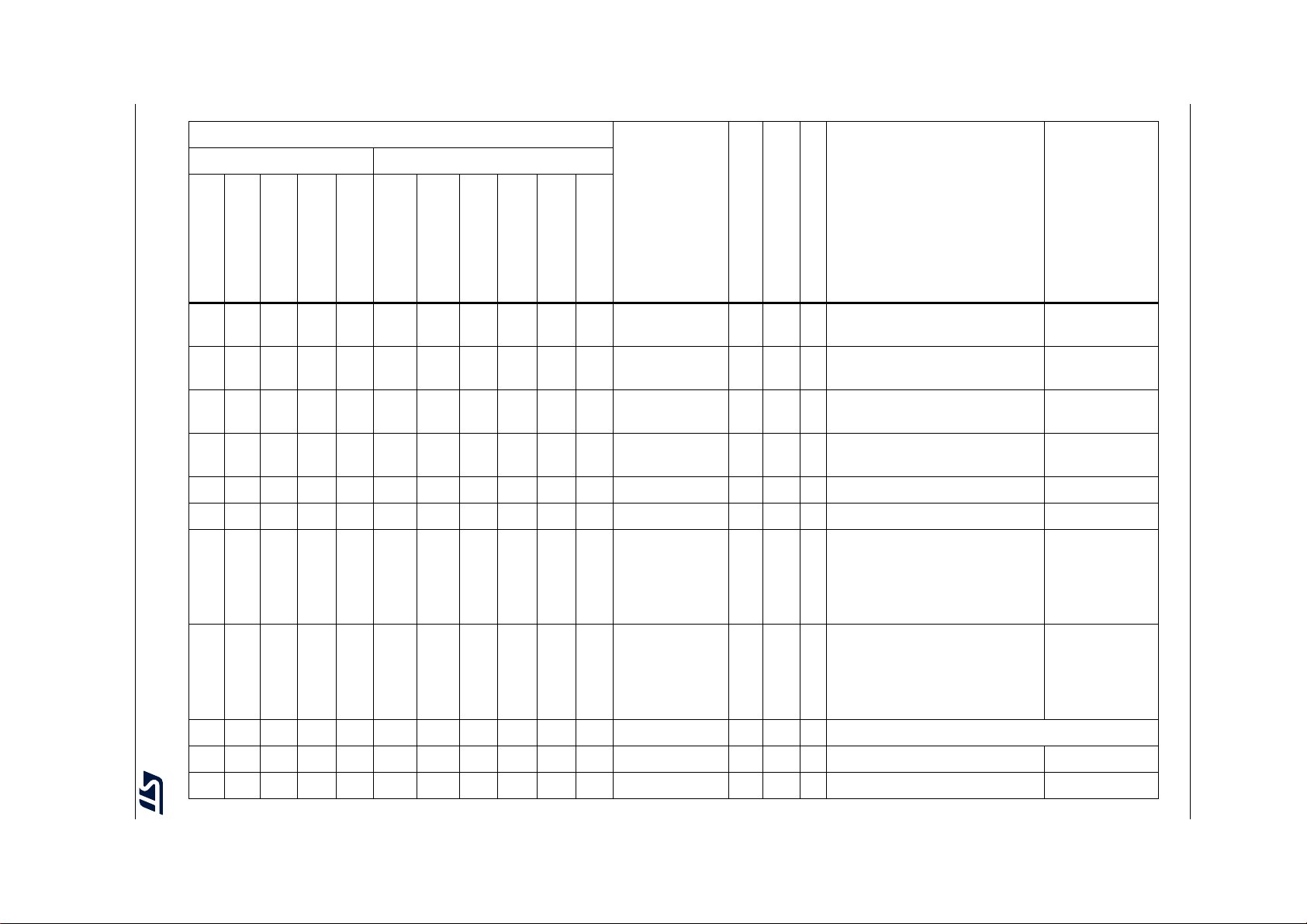
72/230 DS11853 Rev 7
Table 10. STM32F722xx and STM32F723xx pin and ball definition (continued)
Pin Number
STM32F722xx STM32F723xx
Pinouts and pin description STM32F722xx STM32F723xx
Pin name
(function after
reset)
(1)
Pin type
Alternate functions
Notes
Additional
functions
I/O structure
LQFP64
LQFP100
LQFP144
UFBGA176
LQFP176
LQFP100
WLCSP100
UFBGA176
UFBGA144
LQFP144
LQFP176
- - - M13 86 - - M13 - - 86 PH9 I/O FT -
- - - L13 87 - - L13 - - 87 PH10 I/O FT -
- - - L12 88 - - L12 - - 88 PH11 I/O FT -
- - - K12 89 - - K12 - - 89 PH12 I/O FT -
I2C3_SMBA, TIM12_CH2,
FMC_D17, EVENTOUT
TIM5_CH1, FMC_D18,
EVENTOUT
TIM5_CH2, FMC_D19,
EVENTOUT
TIM5_CH3, FMC_D20,
EVENTOUT
- - - H12 90 - - H12 - - 90 VSS S - - - -
- - - J12 91 - K2 J12 - - 91 VDD S - - - -
TIM1_BKIN, I2C2_SMBA,
SPI2_NSS/I2S2_WS,
USART3_CK,
33 51 73 P12 92 51 J2 P12 M11 73 92 PB12 I/O FT
(4)
OTG_HS_ULPI_D5,
OTG_HS_ID, EVENTOUT
-
-
-
-
-
TIM1_CH1N,
34 52 74 P13 93 52 H2 P13 M12 74 93 PB13 I/O FT
(4)
SPI2_SCK/I2S2_CK,
USART3_CTS,
OTG_HS_VBUS
OTG_HS_ULPI_D6, EVENTOUT
- - - - - 53 G2 J15 H11 75 94 OTG_HS_REXT - - - USB HS OTG PHY calibration resistor
- - - - - 54 - - - - - VDDPHYHS - - - - -
- - - - - 55 G1 J14 H10 76 95 VDD12OTGHS - - - - -

Table 10. STM32F722xx and STM32F723xx pin and ball definition (continued)
Pin Number
STM32F722xx STM32F723xx
STM32F722xx STM32F723xx Pinouts and pin description
DS11853 Rev 7 73/230
Pin name
(function after
LQFP64
LQFP100
LQFP144
UFBGA176
LQFP176
LQFP100
WLCSP100
UFBGA176
UFBGA144
LQFP144
LQFP176
35 53 75 R14 94 - - - - - - PB14 I/O FT -
- - - - - 56 J1 R14 L11 77 96 PB14 I/O FT - OTG_HS_DM -
36 54 76 R15 95 - - - - - - PB15 I/O FT -
- - - - - 57 H1 R15 L12 78 97 PB15 I/O FT - OTG_HS_DP -
- 55 77 P15 96 - - P15 L9 79 98 PD8 I/O FT -
reset)
(1)
Pin type
Notes
I/O structure
Alternate functions
TIM1_CH2N, TIM8_CH2N,
SPI2_MISO, USART3_RTS,
TIM12_CH1, SDMMC2_D0,
OTG_HS_DM, EVENTOUT
RTC_REFIN, TIM1_CH3N,
TIM8_CH3N,
SPI2_MOSI/I2S2_SD,
TIM12_CH2, SDMMC2_D1,
OTG_HS_DP, EVENTOUT
USART3_TX, FMC_D13,
EVENTOUT
Additional
functions
-
-
-
- 56 78 P14 97 - - P14 K9 80 99 PD9 I/O FT -
- 57 79 N15 98 - - N15 J9 81 100 PD10 I/O FT -
USART3_RX, FMC_D14,
EVENTOUT
USART3_CK, FMC_D15,
EVENTOUT
-
-

74/230 DS11853 Rev 7
Table 10. STM32F722xx and STM32F723xx pin and ball definition (continued)
Pin Number
STM32F722xx STM32F723xx
Pinouts and pin description STM32F722xx STM32F723xx
Pin name
(function after
LQFP64
LQFP100
LQFP144
UFBGA176
LQFP176
LQFP100
WLCSP100
UFBGA176
UFBGA144
LQFP144
LQFP176
- 58 80 N14 99 58 F3 N14 H9 82 101 PD11 I/O FT -
- 59 81 N13 100 59 F2 N13 L10 83 102 PD12 I/O FT -
- 60 82 M15 101 60 E3 M15 K10 84 103 PD13 I/O FT -
- - 83 - 102 - - - G8 85 104 VSS S - - - -
- - 84 J13 103 - - J13 F8 86 105 VDD S - - - -
reset)
(1)
Pin type
Notes
I/O structure
Alternate functions
USART3_CTS,
QUADSPI_BK1_IO0,
SAI2_SD_A,
FMC_A16/FMC_CLE,
EVENTOUT
TIM4_CH1, LPTIM1_IN1,
USART3_RTS,
QUADSPI_BK1_IO1,
SAI2_FS_A,
FMC_A17/FMC_ALE,
EVENTOUT
TIM4_CH2, LPTIM1_OUT,
QUADSPI_BK1_IO3,
SAI2_SCK_A, FMC_A18,
EVENTOUT
Additional
functions
-
-
-
- 61 85 M14 104 61 F1 M14 K11 87 106 PD14 I/O FT -
- 62 86 L14 105 62 E2 L14 K12 88 107 PD15 I/O FT -
- - 87 L15 106 - - L15 J12 89 108 PG2 I/O FT - FMC_A12, EVENTOUT -
- - 88 K15 107 - - K15 J11 90 109 PG3 I/O FT - FMC_A13, EVENTOUT -
TIM4_CH3, UART8_CTS,
FMC_D0, EVENTOUT
TIM4_CH4, UART8_RTS,
FMC_D1, EVENTOUT
-
-

Table 10. STM32F722xx and STM32F723xx pin and ball definition (continued)
Pin Number
STM32F722xx STM32F723xx
STM32F722xx STM32F723xx Pinouts and pin description
DS11853 Rev 7 75/230
Pin name
(function after
LQFP64
LQFP100
LQFP144
UFBGA176
LQFP176
LQFP100
WLCSP100
UFBGA176
UFBGA144
LQFP144
LQFP176
- - 89 K14 108 - - K14 J10 91 110 PG4 I/O FT -
- - 90 K13 109 - - K13 H12 92 111 PG5 I/O FT -
- - 91 J15 110 - - - - - - PG6 I/O FT - EVENTOUT -
- - 92 J14 111 - - - - - - PG7 I/O FT -
- - 93 H14 112 - - H14 G11 93 112 PG8 I/O FT -
- - 94 G12 113 - - G12 - 94 113 VSS S - - - -
--- - - - - -F10- - VDD --- - -
- - 95 H13 114 - K1 H13 C11 95 114 VDDUSB S - - - -
37 63 96 H15 115 63 E1 H15 G12 96 115 PC6 I/O FT -
reset)
(1)
Pin type
Notes
I/O structure
Alternate functions
FMC_A14/FMC_BA0,
EVENTOUT
FMC_A15/FMC_BA1,
EVENTOUT
USART6_CK, FMC_INT,
EVENTOUT
USART6_RTS, FMC_SDCLK,
EVENTOUT
TIM3_CH1, TIM8_CH1,
I2S2_MCK, USART6_TX,
SDMMC2_D6, SDMMC1_D6,
EVENTOUT
Additional
functions
-
-
-
-
-
38 64 97 G15 116 64 D4 G15 F12 97 116 PC7 I/O FT -
TIM3_CH2, TIM8_CH2,
I2S3_MCK, USART6_RX,
SDMMC2_D7, SDMMC1_D7,
EVENTOUT
-

76/230 DS11853 Rev 7
Table 10. STM32F722xx and STM32F723xx pin and ball definition (continued)
Pin Number
STM32F722xx STM32F723xx
Pinouts and pin description STM32F722xx STM32F723xx
Pin name
(function after
LQFP64
LQFP100
LQFP144
UFBGA176
LQFP176
LQFP100
WLCSP100
UFBGA176
UFBGA144
LQFP144
LQFP176
39 65 98 G14 117 65 D2 G14 F11 98 117 PC8 I/O FT -
40 66 99 F14 118 66 D1 F14 E11 99 118 PC9 I/O FTf -
41 67 100 F15 119 67 D3 F15 E12 100 119 PA8 I/O FTf -
42 68 101 E15 120 68 C3 E15 D12 101 120 PA9 I/O FT -
43 69 102 D15 121 69 C2 D15 D11 102 121 PA10 I/O FT -
reset)
(1)
Pin type
I/O structure
Alternate functions
Notes
TRACED1, TIM3_CH3,
TIM8_CH3, UART5_RTS,
USART6_CK, SDMMC1_D0,
EVENTOUT
MCO2, TIM3_CH4, TIM8_CH4,
I2C3_SDA, I2S_CKIN,
UART5_CTS,
QUADSPI_BK1_IO0,
SDMMC1_D1, EVENTOUT
MCO1, TIM1_CH1, TIM8_BKIN2,
I2C3_SCL, USART1_CK,
OTG_FS_SOF, EVENTOUT
TIM1_CH2, I2C3_SMBA,
SPI2_SCK/I2S2_CK,
USART1_TX, EVENTOUT
TIM1_CH3, USART1_RX,
OTG_FS_ID, EVENTOUT
Additional
functions
-
-
-
OTG_FS_VBUS
-
44 70 103 C15 122 70 C1 C15 C12 103 122 PA11 I/O FT -
45 71 104 B15 123 71 B2 B15 B12 104 123 PA12 I/O FT -
46 72 105 A15 124 72 B1 A15 A12 105 124
PA13(JTMS-
SWDIO)
I/O FT - JTMS-SWDIO, EVENTOUT -
TIM1_CH4, USART1_CTS,
CAN1_RX, OTG_FS_DM,
EVENTOUT
TIM1_ETR, USART1_RTS,
SAI2_FS_B, CAN1_TX,
OTG_FS_DP, EVENTOUT
-
-

Table 10. STM32F722xx and STM32F723xx pin and ball definition (continued)
Pin Number
STM32F722xx STM32F723xx
STM32F722xx STM32F723xx Pinouts and pin description
DS11853 Rev 7 77/230
Pin name
(function after
LQFP64
LQFP100
LQFP144
UFBGA176
LQFP176
LQFP100
WLCSP100
UFBGA176
UFBGA144
LQFP144
LQFP176
- 73 106 F13 125 73 B3 F13 G9 106 125 VCAP_2 S - - - -
47 74 107 F12 126 74 A2 F12 G10 107 126 VSS S - - - -
48 75 108 G13 127 75 A1 G13 F9 108 127 VDD S - - - -
- - - E12 128 - - E12 - - 128 PH13 I/O FT -
- - - E13 129 - - E13 - - 129 PH14 I/O FT -
- - - D13 130 - - D13 - - 130 PH15 I/O FT -
- - - E14 131 - - E14 - - 131 PI0 I/O FT -
- - - D14 132 - - D14 - - 132 PI1 I/O FT -
reset)
(1)
Pin type
Notes
I/O structure
Alternate functions
TIM8_CH1N, UART4_TX,
CAN1_TX, FMC_D21,
EVENTOUT
TIM8_CH2N, UART4_RX,
CAN1_RX, FMC_D22,
EVENTOUT
TIM8_CH3N, FMC_D23,
EVENTOUT
TIM5_CH4, SPI2_NSS/I2S2_WS,
FMC_D24, EVENTOUT
TIM8_BKIN2,
SPI2_SCK/I2S2_CK, FMC_D25,
EVENTOUT
Additional
functions
-
-
-
-
-
- - - C14 133 - - C14 - - 133 PI2 I/O FT -
- - - C13 134 - - C13 - - 134 PI3 I/O FT -
- - - D9 135 - - D9 - - 135 VSS S - - - -
TIM8_CH4, SPI2_MISO,
FMC_D26, EVENTOUT
TIM8_ETR,
SPI2_MOSI/I2S2_SD, FMC_D27,
EVENTOUT
-
-

78/230 DS11853 Rev 7
Table 10. STM32F722xx and STM32F723xx pin and ball definition (continued)
Pin Number
STM32F722xx STM32F723xx
Pinouts and pin description STM32F722xx STM32F723xx
Pin name
(function after
LQFP64
LQFP100
LQFP144
UFBGA176
LQFP176
LQFP100
WLCSP100
UFBGA176
UFBGA144
LQFP144
LQFP176
- - - C9 136 - - C9 - - 136 VDD S - - - -
49 76 109 A14 137 76 C4 A14 A11 109 137
50 77 110 A13 138 77 B4 A13 A10 110 138 PA15(JTDI) I/O FT -
51 78 111 B14 139 78 A3 B14 B11 111 139 PC10 I/O FT -
52 79 112 B13 140 79 C5 B13 B10 112 140 PC11 I/O FT -
53 80 113 A12 141 80 D5 A12 C10 113 141 PC12 I/O FT -
PA14(JTCK-
(1)
reset)
SWCLK)
Pin type
I/O FT - JTCK-SWCLK, EVENTOUT -
Notes
I/O structure
Alternate functions
JTDI, TIM2_CH1/TIM2_ETR,
SPI1_NSS/I2S1_WS,
SPI3_NSS/I2S3_WS,
UART4_RTS, EVENTOUT
SPI3_SCK/I2S3_CK,
USART3_TX, UART4_TX,
QUADSPI_BK1_IO1,
SDMMC1_D2, EVENTOUT
SPI3_MISO, USART3_RX,
UART4_RX,
QUADSPI_BK2_NCS,
SDMMC1_D3, EVENTOUT
TRACED3,
SPI3_MOSI/I2S3_SD,
USART3_CK, UART5_TX,
SDMMC1_CK, EVENTOUT
Additional
functions
-
-
-
-
- 81 114 B12 142 81 B5 B12 E10 114 142 PD0 I/O FT -
- 82 115 C12 143 82 A4 C12 D10 115 143 PD1 I/O FT -
CAN1_RX, FMC_D2,
EVENTOUT
CAN1_TX, FMC_D3,
EVENTOUT
-
-

Table 10. STM32F722xx and STM32F723xx pin and ball definition (continued)
Pin Number
STM32F722xx STM32F723xx
STM32F722xx STM32F723xx Pinouts and pin description
DS11853 Rev 7 79/230
Pin name
(function after
LQFP64
LQFP100
LQFP144
UFBGA176
LQFP176
LQFP100
WLCSP100
UFBGA176
UFBGA144
LQFP144
LQFP176
54 83 116 D12 144 83 E5 D12 E9 116 144 PD2 I/O FT -
- 84 117 D11 145 84 C6 D11 D9 117 145 PD3 I/O FT -
- 85 118 D10 146 85 B6 D10 C9 118 146 PD4 I/O FT -
- 86 119 C11 147 86 A5 C11 B9 119 147 PD5 I/O FT -
- - 120 D8 148 - - D8 E7 120 148 VSS S - - - -
- - 121 C8 149 - - C8 F7 121 149 VDDSDMMC S - - - -
- 87 122 B11 150 87 D6 B11 A8 122 150 PD6 I/O FT -
reset)
(1)
Pin type
Notes
I/O structure
Alternate functions
TRACED2, TIM3_ETR,
UART5_RX, SDMMC1_CMD,
EVENTOUT
SPI2_SCK/I2S2_CK,
USART2_CTS, FMC_CLK,
EVENTOUT
USART2_RTS, FMC_NOE,
EVENTOUT
USART2_TX, FMC_NWE,
EVENTOUT
SPI3_MOSI/I2S3_SD,
SAI1_SD_A, USART2_RX,
SDMMC2_CK, FMC_NWAIT,
EVENTOUT
Additional
functions
-
-
-
-
-
- 88 123 A11 151 88 E6 A11 A9 123 151 PD7 I/O FT -
- - 124 C10 152 - - C10 E8 124 152 PG9 I/O FT -
USART2_CK SDMMC2_CMD,
FMC_NE1, EVENTOUT
USART6_RX,
QUADSPI_BK2_IO2,
SAI2_FS_B, SDMMC2_D0,
FMC_NE2/FMC_NCE,
EVENTOUT
-
-
80/230 DS11853 Rev 7
Table 10. STM32F722xx and STM32F723xx pin and ball definition (continued)
Pin Number
STM32F722xx STM32F723xx
Pinouts and pin description STM32F722xx STM32F723xx
Pin name
(function after
LQFP64
LQFP100
LQFP144
UFBGA176
LQFP176
LQFP100
WLCSP100
UFBGA176
UFBGA144
LQFP144
LQFP176
- - 125 B10 153 - - B10 D8 125 153 PG10 I/O FT -
- - 126 B9 154 - - B9 C8 126 154 PG11 I/O FT -
- - 127 B8 155 - - B8 B8 127 155 PG12 I/O FT -
- - 128 A8 156 - - A8 D7 128 156 PG13 I/O FT -
reset)
(1)
Pin type
I/O structure
Alternate functions
Notes
SAI2_SD_B, SDMMC2_D1,
FMC_NE3, EVENTOUT
SDMMC2_D2, FMC_INT,
EVENTOUT
LPTIM1_IN1, USART6_RTS,
SDMMC2_D3, FMC_NE4,
EVENTOUT
TRACED0, LPTIM1_OUT,
USART6_CTS, FMC_A24,
EVENTOUT
Additional
functions
-
-
-
-
TRACED1, LPTIM1_ETR,
- - 129 A7 157 - - A7 C7 129 157 PG14 I/O FT -
- - 130 D7 158 - - D7 - 130 158 VSS S - - - -
QUADSPI_BK2_IO3, FMC_A25,
USART6_TX,
EVENTOUT
-
Table 10. STM32F722xx and STM32F723xx pin and ball definition (continued)
Pin Number
STM32F722xx STM32F723xx
STM32F722xx STM32F723xx Pinouts and pin description
DS11853 Rev 7 81/230
Pin name
(function after
reset)
(1)
Pin type
Alternate functions
Notes
Additional
functions
I/O structure
LQFP64
LQFP100
LQFP144
UFBGA176
LQFP176
LQFP100
WLCSP100
UFBGA176
UFBGA144
LQFP144
LQFP176
- - 131 C7 159 - - C7 F6 131 159 VDD S - - - -
- - 132 B7 160 - - B7 B7 132 160 PG15 I/O FT -
USART6_CTS, FMC_SDNCAS,
EVENTOUT
JTDO/TRACESWO, TIM2_CH2,
55 89 133 A10 161 89 A6 A10 A7 133 161
PB3(JTDO/TRA
CESWO)
I/O FT -
SPI1_SCK/I2S1_CK,
SPI3_SCK/I2S3_CK,
SDMMC2_D2, EVENTOUT
NJTRST, TIM3_CH1,
56 90 134 A9 162 90 B7 A9 A6 134 162 PB4(NJTRST) I/O FT -
SPI1_MISO, SPI3_MISO,
SPI2_NSS/I2S2_WS,
SDMMC2_D3, EVENTOUT
TIM3_CH2, I2C1_SMBA,
SPI1_MOSI/I2S1_SD,
SPI3_MOSI/I2S3_SD,
57 91 135 A6 163 91 C7 A6 B6 135 163 PB5 I/O FT
(4)
OTG_HS_ULPI_D7,
FMC_SDCKE1, EVENTOUT
-
-
-
-
58 92 136 B6 164 92 D7 B6 C6 136 164 PB6 I/O FTf -
TIM4_CH1, I2C1_SCL,
USART1_TX,
QUAD SPI_BK1_NCS,
FMC_SDNE1, EVENTOUT
-

82/230 DS11853 Rev 7
Table 10. STM32F722xx and STM32F723xx pin and ball definition (continued)
Pin Number
STM32F722xx STM32F723xx
Pinouts and pin description STM32F722xx STM32F723xx
Pin name
(function after
LQFP64
LQFP100
LQFP144
UFBGA176
LQFP176
LQFP100
WLCSP100
UFBGA176
UFBGA144
LQFP144
LQFP176
59 93 137 B5 165 93 B8 B5 D6 137 165 PB7 I/O FTf -
60 94 138 D6 166 94 A7 D6 D5 138 166 BOOT I B - - VPP
61 95 139 A5 167 95 C8 A5 C5 139 167 PB8 I/O FTf -
62 96 140 B4 168 96 D8 B4 B5 140 168 PB9 I/O FTf -
reset)
(1)
Pin type
Notes
I/O structure
Alternate functions
TIM4_CH2, I2C1_SDA,
USART1_RX, FMC_NL,
EVENTOUT
TIM4_CH3, TIM10_CH1,
I2C1_SCL, CAN1_RX,
SDMMC2_D4, SDMMC1_D4,
EVENTOUT
TIM4_CH4, TIM11_CH1,
I2C1_SDA, SPI2_NSS/I2S2_WS,
CAN1_TX, SDMMC2_D5,
SDMMC1_D5, EVENTOUT
Additional
functions
-
-
-
TIM4_ETR, LPTIM1_ETR,
- 97 141 A4 169 97 E7 A4 A5 141 169 PE0 I/O FT -
- 98 142 A3 170 98 B9 A3 A4 142 170 PE1 I/O FT -
63 99 - D5 - 99 A8 D5 E6 - - VSS S - - - -
UART8_Rx, SAI2_MCK_A,
FMC_NBL0, EVENTOUT
LPTIM1_IN2, UART8_Tx,
FMC_NBL1, EVENTOUT
-
-
Table 10. STM32F722xx and STM32F723xx pin and ball definition (continued)
Pin Number
STM32F722xx STM32F723xx
STM32F722xx STM32F723xx Pinouts and pin description
DS11853 Rev 7 83/230
Pin name
(function after
LQFP64
LQFP100
LQFP144
UFBGA176
LQFP176
LQFP100
WLCSP100
UFBGA176
UFBGA144
LQFP144
LQFP176
- - 143 C6 171 - - C6 E5 143 171 PDR_ON S - - - -
64 100 144 C5 172 100 A9 C5 F5 144 172 VDD S - - - -
- - - D4 173 - - D4 - - 173 PI4 I/O FT -
- - - C4 174 - - C4 - - 174 PI5 I/O FT -
- - - C3 175 - - C3 - - 175 PI6 I/O FT -
- - - C2 176 - - C2 - - 176 PI7 I/O FT -
reset)
(1)
Pin type
Notes
I/O structure
Alternate functions
TIM8_BKIN, SAI2_MCK_A,
FMC_NBL2, EVENTOUT
TIM8_CH1, SAI2_SCK_A,
FMC_NBL3, EVENTOUT
TIM8_CH2, SAI2_SD_A,
FMC_D28, EVENTOUT
TIM8_CH3, SAI2_FS_A,
FMC_D29, EVENTOUT
Additional
functions
-
-
-
-
- - - F6 - - - F6 - - - VSS S - - - -
- - - F7 - - - F7 - - - VSS S - - - -
- - - F8 - - - F8 - - - VSS S - - - -
- - - F9 - - - F9 - - - VSS S - - - -
- - - F10 - - - F10 - - - VSS S - - - -
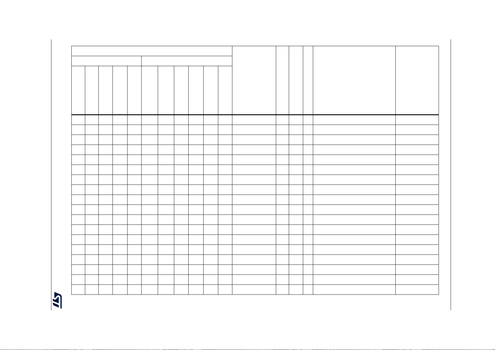
84/230 DS11853 Rev 7
Table 10. STM32F722xx and STM32F723xx pin and ball definition (continued)
Pin Number
STM32F722xx STM32F723xx
Pinouts and pin description STM32F722xx STM32F723xx
Pin name
(function after
LQFP64
LQFP100
LQFP144
UFBGA176
LQFP176
LQFP100
WLCSP100
UFBGA176
UFBGA144
LQFP144
LQFP176
- - - G6 - - - G6 - - - VSS S - - - -
- - - G7 - - - G7 - - - VSS S - - - -
- - - G8 - - - G8 - - - VSS S - - - -
- - - G9 - - - G9 - - - VSS S - - - -
- - - G10 - - - G10 - - - VSS S - - - -
- - - H6 - - - H6 - - - VSS S - - - -
- - - H7 - - - H7 - - - VSS S - - - -
- - - H8 - - - H8 - - - VSS S - - - -
- - - H9 - - - H9 - - - VSS S - - - -
- - - H10 - - - H10 - - - VSS S - - - -
- - - J6 - - - J6 - - - VSS S - - - -
- - - J7 - - - J7 - - - VSS S - - - -
- - - J8 - - - J8 - - - VSS S - - - -
reset)
(1)
Pin type
Notes
I/O structure
Alternate functions
Additional
functions
- - - J9 - - - J9 - - - VSS S - - - -
- - - J10 - - - J10 - - - VSS S - - - -
- - - K6 - - - K6 - - - VSS S - - - -
- - - K7 - - - K7 - - - VSS S - - - -
- - - K8 - - - K8 - - - VSS S - - - -

Table 10. STM32F722xx and STM32F723xx pin and ball definition (continued)
Pin Number
STM32F722xx STM32F723xx
STM32F722xx STM32F723xx Pinouts and pin description
DS11853 Rev 7 85/230
Pin name
(function after
reset)
(1)
Pin type
Alternate functions
Notes
Additional
functions
I/O structure
LQFP64
LQFP100
LQFP144
UFBGA176
LQFP176
LQFP100
WLCSP100
UFBGA176
UFBGA144
LQFP144
LQFP176
- - - K9 - - - K9 - - - VSS S - - - -
- - - K10 - - - K10 - - - VSS S - - - -
1. Function availability depends on the chosen device.
2. PC13, PC14, PC15 and PI8 are supplied through the power switch. Since the switch only sinks a limited amount of current (3 mA), the use of GPIOs PC13 to PC15 and
PI8 in output mode is limited:
- The speed should not exceed 2 MHz with a maximum load of 30 pF.
- These I/Os must not be used as a current source (e.g. to drive an LED).
3. Main function after the first backup domain power-up. Later on, it depends on the contents of the RTC registers even after reset (because these registers are not reset by
the main reset).
4. ULPI signals not available on the STM32F723xx devices.
5. If the device is in regulator OFF/internal reset ON mode (BYPASS_REG pin is set to VDD), then PA0 is used as an internal reset (active low).
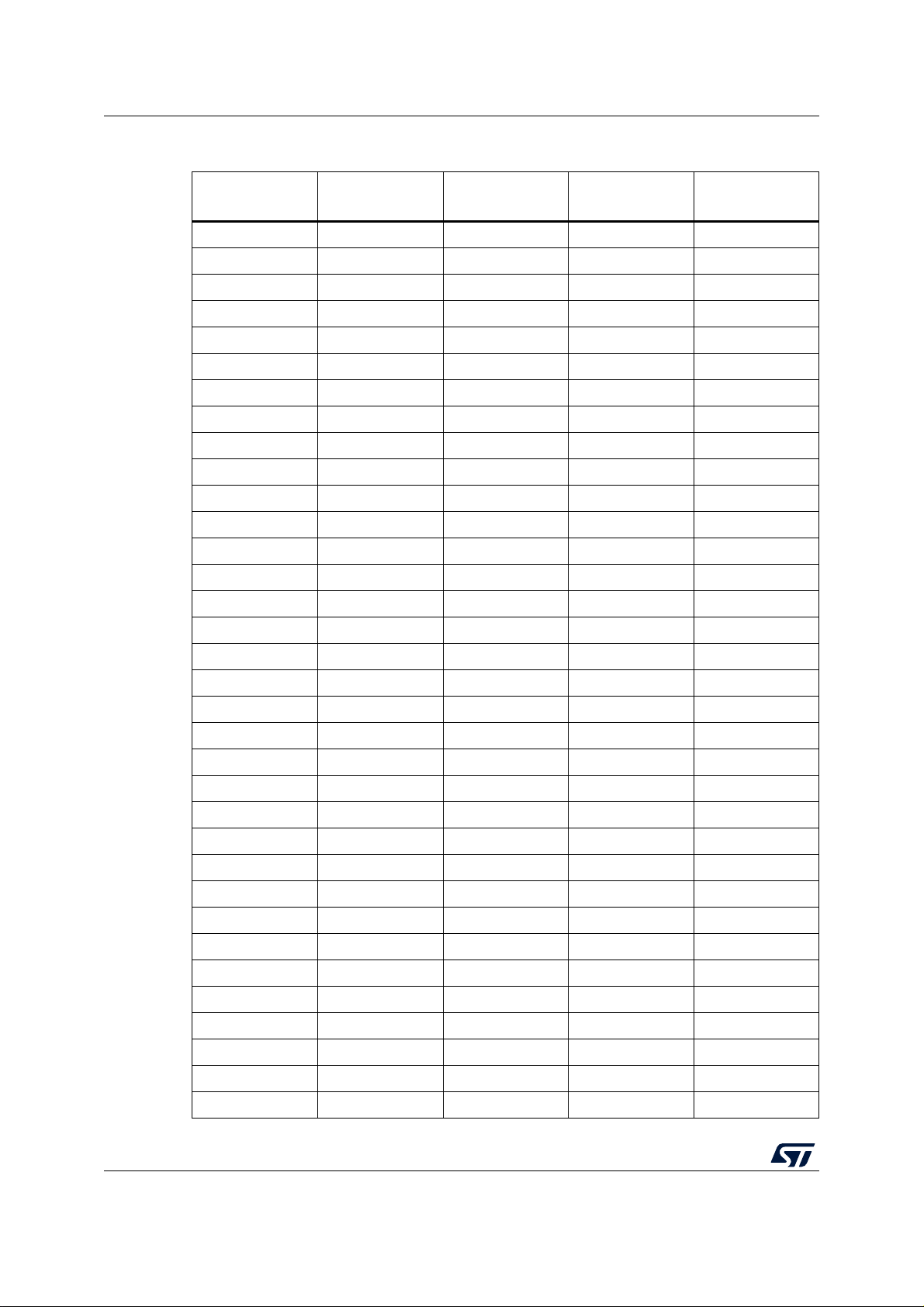
Pinouts and pin description STM32F722xx STM32F723xx
Pin name
NOR/PSRAM/SRAMNOR/PSRAM
Table 11. FMC pin definition
Mux
NAND16 SDRAM
PF0 A0 - - A0
PF1 A1 - - A1
PF2 A2 - - A2
PF3 A3 - - A3
PF4 A4 - - A4
PF5 A5 - - A5
PF12 A6 - - A6
PF13 A7 - - A7
PF14 A8 - - A8
PF15 A9 - - A9
PG0 A10 - - A10
PG1 A11 - - A11
PG2 A12 - - A12
PG3 A13 - - -
PG4 A14 - - BA0
PG5 A15 - - BA1
PD11 A16 A16 CLE -
PD12 A17 A17 ALE -
PD13 A18 A18 - -
PE3 A19 A19 - -
PE4 A20 A20 - -
PE5 A21 A21 - -
PE6 A22 A22 - -
PE2 A23 A23 - -
PG13 A24 A24 - -
PG14 A25 A25 - -
PD14 D0 DA0 D0 D0
PD15 D1 DA1 D1 D1
PD0 D2 DA2 D2 D2
PD1 D3 DA3 D3 D3
PE7 D4 DA4 D4 D4
PE8 D5 DA5 D5 D5
PE9 D6 DA6 D6 D6
PE10 D7 DA7 D7 D7
86/230 DS11853 Rev 7

STM32F722xx STM32F723xx Pinouts and pin description
Table 11. FMC pin definition (continued)
Pin name
NOR/PSRAM/SRAMNOR/PSRAM
Mux
NAND16 SDRAM
PE11 D8 DA8 D8 D8
PE12 D9 DA9 D9 D9
PE13 D10 DA10 D10 D10
PE14 D11 DA11 D11 D11
PE15 D12 DA12 D12 D12
PD8 D13 DA13 D13 D13
PD9 D14 DA14 D14 D14
PD10 D15 DA15 D15 D15
PH8 D16 - - D16
PH9 D17 - - D17
PH10 D18 - - D18
PH11 D19 - - D19
PH12 D20 - - D20
PH13 D21 - - D21
PH14 D22 - - D22
PH15 D23 - - D23
PI0 D24 - - D24
PI1 D25 - - D25
PI2 D26 - - D26
PI3 D27 - - D27
PI6 D28 - - D28
PI7 D29 - - D29
PI9 D30 - - D30
PI10 D31 - - D31
PD7 NE1 NE1 - -
PG9 NE2 NE2 NCE -
PG10 NE3 NE3 - -
PG11----
PG12 NE4 NE4 - -
PD3 CLK CLK - -
PD4 NOE NOE NOE -
PD5 NWE NWE NWE -
PD6 NWAIT NWAIT NWAIT -
PB7 NADV NADV - -
DS11853 Rev 7 87/230
99

Pinouts and pin description STM32F722xx STM32F723xx
Table 11. FMC pin definition (continued)
Pin name
PF6 - - - -
PF7 - - - -
PF8 - - - -
PF9 - - - -
PF10----
PG6 - - - -
PG7 - - INT -
PE0 NBL0 NBL0 - NBL0
PE1 NBL1 NBL1 - NBL1
PI4 NBL2 - - NBL2
PI5 NBL3 - - NBL3
PG8 - - - SDCLK
PC0 - - - SDNWE
PF11 - - - SDNRAS
PG15 - - - SDNCAS
PH2 - - - SDCKE0
PH3 - - - SDNE0
NOR/PSRAM/SRAMNOR/PSRAM
Mux
NAND16 SDRAM
PH6 - - - SDNE1
PH7 - - - SDCKE1
PH5 - - - SDNWE
PC2 - - - SDNE0
PC3 - - - SDCKE0
PB5 - - - SDCKE1
PB6 - - - SDNE1
88/230 DS11853 Rev 7
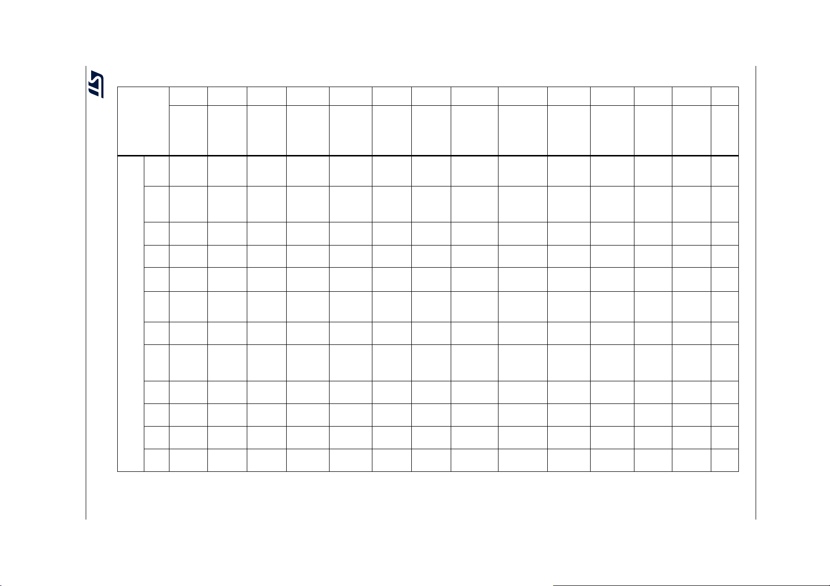
Table 12. STM32F722xx and STM32F723xx alternate function mapping
AF0 AF1 AF2 AF3 AF4 AF5 AF6 AF7 AF8 AF9 AF10 AF11 AF12 AF15
STM32F722xx STM32F723xx Pinouts and pin description
DS11853 Rev 7 89/230
O
D
SPI2/I2S2/
SPI3/I2S3/
SPI3/I2S3/
SAI1/
UART4
SPI3_NSS
/I2S3_WS
SPI2/I2S2/S
PI3/I2S3/US
ART1/2/3/UA
RT5
USART2_CT
S
USART2_RT
S
USART2_CK - - - -
-- - -
- - - TIM13_CH1 - - -
- - - TIM14_CH1 - -
- USART1_TX - - - - -
USART1_CT
S
SAI2/USART
6/UART4/5/7/
8/OTG1_FS
UART4_ TX - SAI2_SD_B - -
UART4_RX
-
-
SPI1/I2S1/
SPI2/I2S2/
SPI3/I2S3/
SPI4/5
SPI1_NSS
/I2S1_WS
SPI1_SCK
/I2S1_CK
SPI1_MIS
SPI1_MO
SI/I2S1_S
/I2S2_CK
Port
PA0 -
PA1 - TIM2_CH2 TIM5_CH2 - - - -
PA2 - TIM2_CH3 TIM5_CH3 TIM9_CH1 - - - USART2_TX SAI2_SCK_B - - - -
PA3 - TIM2_CH4 TIM5_CH4 TIM9_CH2 - - - USART2_RX - -
PA4 - - - - -
PA5 -
Port A
PA6 -
PA7 -
PA8 MCO1 TIM1_CH1 -
PA9 - TI M1_ CH2 - -
PA10 - TIM1_CH3 - - - - - USART1_RX - -
PA11 - TI M1 _CH 4 - - - - -
SYS TIM1/2 TIM3/4/5
TIM2_CH1
/TIM2_ETRTIM5_CH1 TIM8_ETR - - -
TIM2_CH1
/TIM2_ET
R
TIM1_BKI
TIM1_CH1
TIM3_CH1 TIM8_BKIN -
N
TIM3_CH2
N
-
TIM8/9/10/1
1/LPTIM1
TIM8_CH1
N
TIM8_CH1
N
TIM8_BKIN
2
I2C1/2/3/U
SART1
I2C3_SCL - - USART1_CK - -
I2C3_SMBASPI2_SCK
CAN1/TIM1
2/13/14/QU
ADSPI/
FMC/
OTG2_HS
QUADSPI_
BK1_IO3
- CAN1_RX
SAI2/QUAD
SPI/SDMM
C2/OTG2_
HS/OTG1_
FS
SAI2_MCK
_B
OTG_HS_U
LPI_D0
OTG_HS_U
LPI_CK
OTG_FS_S
OF
OTG_FS_I
D
OTG_FS_D
M
UART7/F
SDMMC2
MC/SDM
MC1/
OTG2_FS
--
--
OTG_HS_
SOF
--
FMC_SDNWEEVEN
--
--
--
SYS
EVEN
TOUT
EVEN
TOUT
EVEN
TOUT
EVEN
TOUT
EVEN
TOUT
EVEN
TOUT
EVEN
TOUT
TOUT
EVEN
TOUT
EVEN
TOUT
EVEN
TOUT
EVEN
TOUT

90/230 DS11853 Rev 7
Table 12. STM32F722xx and STM32F723xx alternate function mapping (continued)
AF0 AF1 AF2 AF3 AF4 AF5 AF6 AF7 AF8 AF9 AF10 AF11 AF12 AF15
Pinouts and pin description STM32F722xx STM32F723xx
Port
PA12 - TIM1_ETR - - - - -
PA1 3
Port A
PA1 4
PA1 5 JT DI
PB0 -
PB1 -
PB2 - - - - - -
PB3
PB4 NJTRST - TIM3_CH1 - -
Port B
PB5 - - TIM3_CH2 -
PB6 - - TIM4_CH1 - I2C1_SCL - - USART1_TX - -
PB7 - - TIM4_CH2 - I2C1_SDA - - USART1_RX - - - - FMC_NL
PB8 - - TIM4_CH3
SYS TIM1/2 TIM3/4/5
JTMS-
SWDIO
JTCK-
SWCLK
JTDO/TR
ACESWO
-- - - -- - - - - --
-- - - -- - - - - --
TIM2_CH1
/TIM2_ET
R
TIM1_CH2
TIM1_CH3
TIM2_CH2 - - -
N
N
TIM3_CH3
TIM3_CH4
TIM8/9/10/1
1/LPTIM1
-- -
TIM8_CH2
TIM8_CH3
TIM10_CH
I2C1/2/3/U
SART1
N
N
I2C1_SMB
I2C1_SCL - - - - CAN1_RX
1
SPI1/I2S1/
SPI2/I2S2/
SPI3/I2S3/
SPI4/5
SPI1_NSS
/I2S1_WS
- - - - UART4_CTS
--- - -
SPI1_SCK
/I2S1_CK
SPI1_MISOSPI3_MISOSPI2_NSS/I2
SPI1_MO
SI/I2S1_S
A
SPI2/I2S2/
SPI3/I2S3/
SPI3/I2S3/
SAI1/
UART4
SPI3_NSS
/I2S3_WS
SAI1_SD_ASPI3_MOSI/I
SPI3_SCK
/I2S3_CK
SPI3_MO
SI/I2S3_S
D
D
SPI2/I2S2/S
PI3/I2S3/US
ART1/2/3/UA
RT5
USART1_RT
S
2S3_SD
S2_WS
SAI2/USART
6/UART4/5/7/
8/OTG1_FS
SAI2_FS_B CAN1_TX
- UART4_RTS - - - -
---
---
CAN1/TIM1
2/13/14/QU
ADSPI/
FMC/
OTG2_HS
-
--
QUADSPI_
CLK
-
-
SAI2/QUAD
SPI/SDMM
C2/OTG2_
HS/OTG1_
OTG_FS_D
OTG_HS_U
LPI_D1
OTG_HS_U
LPI_D2
SDMMC2_
SDMMC2_
OTG_HS_U
LPI_D7
QUADSPI_
BK1_NCS
SDMMC2_
SDMMC2
FS
P
---
D2
D3
D4
UART7/F
MC/SDM
MC1/
OTG2_FS
--
--
--
--
--
FMC_SDC
-
-
-
KE1
FMC_SDNE1EVEN
SDMMC1
_D4
SYS
EVEN
TOUT
EVEN
TOUT
EVEN
TOUT
EVEN
TOUT
EVEN
TOUT
EVEN
TOUT
EVEN
TOUT
EVEN
TOUT
EVEN
TOUT
EVEN
TOUT
TOUT
EVEN
TOUT
EVEN
TOUT
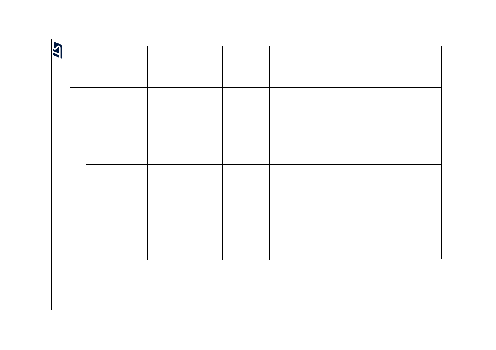
Table 12. STM32F722xx and STM32F723xx alternate function mapping (continued)
AF0 AF1 AF2 AF3 AF4 AF5 AF6 AF7 AF8 AF9 AF10 AF11 AF12 AF15
STM32F722xx STM32F723xx Pinouts and pin description
DS11853 Rev 7 91/230
-
-
SPI1/I2S1/
SPI2/I2S2/
SPI3/I2S3/
SPI4/5
SPI2_NSS
/I2S2_WS
SPI2_SCK
/I2S2_CK
/I2S2_WS
SPI2_SCK
/I2S2_CK
SPI2_MIS
SPI2_MO
SI/I2S2_S
SPI2_MO
SI/I2S2_S
SPI2_MIS
SPI2_MO
SI/I2S2_S
Port
PB9 - - TIM4_CH4 TIM11_CH1 I2C1_SDA
PB10 - TIM2_CH3 - - I2C2_SCL
PB11 - TIM2_CH4 - - I2C2_SDA - - USART3_RX - -
Port B
PB12 -
PB13 -
PB14 -
PB15
PC0--- - - -- -SAI2_FS_B-
PC1 TRACED0 - - - -
Port C
PC2 - - - - -
PC3 - - - - -
SYS TIM1/2 TIM3/4/5
TIM1_BKI
N
TIM1_CH1
N
TIM1_CH2
N
RTC_REFINTIM1_CH3
N
TIM8/9/10/1
1/LPTIM1
--
-- -
TIM8_CH2
-
TIM8_CH3
-
I2C1/2/3/U
SART1
I2C2_SMBASPI2_NSS
N
N
O
D
D
O
D
SPI2/I2S2/
SPI3/I2S3/
SPI3/I2S3/
SAI1/
UART4
SAI1_SD_
SPI2/I2S2/S
PI3/I2S3/US
ART1/2/3/UA
RT5
- - - CAN1_TX
- USART3_TX - -
- USART3_CK - -
USART3_CT
-
-
- - - TIM12_CH2
A
-- - -
-- - -
S
USART3_RT
S
SAI2/USART
6/UART4/5/7/
8/OTG1_FS
--
- TIM12_CH1
------
CAN1/TIM1
2/13/14/QU
ADSPI/
FMC/
OTG2_HS
SAI2/QUAD
SPI/SDMM
C2/OTG2_
HS/OTG1_
FS
SDMMC2_
D5
OTG_HS_U
LPI_D3
OTG_HS_U
LPI_D4
OTG_HS_U
LPI_D5
OTG_HS_U
LPI_D6
SDMMC2_
D0
SDMMC2_
D1
OTG_HS_U
LPI_STP
OTG_HS_U
LPI_DIR
OTG_HS_U
LPI_NXT
UART7/F
SDMMC2
MC/SDM
MC1/
OTG2_FS
SDMMC1
-
--
--
-
--
-
-
-
-
-
_D5
OTG_HS_IDEVEN
OTG_HS_DMEVEN
OTG_HS_DPEVEN
FMC_SDNWEEVEN
FMC_SDNE0EVEN
FMC_SDC
KE0
SYS
EVEN
TOUT
EVEN
TOUT
EVEN
TOUT
TOUT
EVEN
TOUT
TOUT
TOUT
TOUT
EVEN
TOUT
TOUT
EVEN
TOUT

92/230 DS11853 Rev 7
Table 12. STM32F722xx and STM32F723xx alternate function mapping (continued)
AF0 AF1 AF2 AF3 AF4 AF5 AF6 AF7 AF8 AF9 AF10 AF11 AF12 AF15
Pinouts and pin description STM32F722xx STM32F723xx
Port
SYS TIM1/2 TIM3/4/5
PC4 - - - - - I2S1_MCK - - - - - -
PC5--- - - -- - - - - -
PC6 - - TIM3_CH1 TIM8_CH1 - I2S2_MCK - - USART6_TX -
PC7 - - TIM3_CH2 TIM8_CH2 - - I2S3_MCK - USART6_RX -
PC8 TRACED1 - TIM3_CH3 TIM8_CH3 - - - UART5_RTS USART6_CK - - -
PC9 MCO2 - TIM3_CH4 TIM8_CH4 I2C3_SDA I2S_CKIN - UART5_CTS -
Port C
PC10---- --
PC11---- --
PC12 TRACED3 - - - - -
PC13---- --- - - - ---
PC14---- --- - - - ---
PC15---- --- - - - ---
TIM8/9/10/1
1/LPTIM1
I2C1/2/3/U
SART1
SPI1/I2S1/
SPI2/I2S2/
SPI3/I2S3/
SPI4/5
SPI2/I2S2/
SPI3/I2S3/
SPI3/I2S3/
SAI1/
UART4
SPI3_SCK
/I2S3_CK
SPI3_MIS
SPI3_MO
SI/I2S3_SDUSART3_CK UART5_TX - - -
SPI2/I2S2/S
PI3/I2S3/US
ART1/2/3/UA
RT5
USART3_TX UART4_TX
USART3_RX UART4_RX
O
SAI2/USART
6/UART4/5/7/
8/OTG1_FS
CAN1/TIM1
2/13/14/QU
ADSPI/
FMC/
OTG2_HS
QUADSPI_
BK1_IO0
QUADSPI_
BK1_IO1
QUADSPI_
BK2_NCS
SAI2/QUAD
SPI/SDMM
C2/OTG2_
HS/OTG1_
FS
SDMMC2_
D6
SDMMC2_
D7
SDMMC2
--
--
--
-
-
UART7/F
MC/SDM
MC1/
OTG2_FS
FMC_SDNE0EVEN
FMC_SDC
KE0
SDMMC1
_D6
SDMMC1
_D7
SDMMC1
_D0
SDMMC1
_D1
SDMMC1
_D2
SDMMC1
_D3
SDMMC1
_CK
SYS
TOUT
EVEN
TOUT
EVEN
TOUT
EVEN
TOUT
EVEN
TOUT
EVEN
TOUT
EVEN
TOUT
EVEN
TOUT
EVEN
TOUT
EVEN
TOUT
EVEN
TOUT
EVEN
TOUT

Table 12. STM32F722xx and STM32F723xx alternate function mapping (continued)
AF0 AF1 AF2 AF3 AF4 AF5 AF6 AF7 AF8 AF9 AF10 AF11 AF12 AF15
STM32F722xx STM32F723xx Pinouts and pin description
DS11853 Rev 7 93/230
D
SPI2/I2S2/
SPI3/I2S3/
SPI3/I2S3/
SAI1/
UART4
-
SAI1_SD_
A
SPI2/I2S2/S
PI3/I2S3/US
ART1/2/3/UA
RT5
USART2_CT
S
USART2_RT
S
USART2_RX - - -
USART3_CT
S
USART3_RT
S
SAI2/USART
6/UART4/5/7/
8/OTG1_FS
Port
SYS TIM1/2 TIM3/4/5
PD0--- - - -- - -CAN1_RX- -FMC_D2
PD1--- - - -- - -CAN1_TX- -FMC_D3
PD2 TRACED2 - TIM3_ETR - - - - - UART5_RX - - -
PD3 - - - - -
PD4--- - - --
PD5--- - - --USART2_TX- - - -
PD6 - - - - -
Port D
PD7--- - - --USART2_CK- - -
PD8 - - - - - - - USART3_TX - - - - FMC_D13
PD9--- - - --USART3_RX- - - -FMC_D14
PD10 - - - - - - - USART3_CK - - - - FMC_D15
PD11---- ---
PD12 - - TIM4_CH1
PD13 - - TIM4_CH2
PD14 - - TIM4_CH3 - - - - - UART8_CTS - - - FMC_D0
Port D
PD15 - - TIM4_CH4 - - - - - UART8_RTS - - - FMC_D1
TIM8/9/10/1
1/LPTIM1
LPTIM1_IN
1
LPTIM1_O
UT
I2C1/2/3/U
SART1
SPI1/I2S1/
SPI2/I2S2/
SPI3/I2S3/
SPI4/5
SPI2_SCK
/I2S2_CK
SPI3_MO
SI/I2S3_S
---
--- - -
CAN1/TIM1
2/13/14/QU
ADSPI/
FMC/
OTG2_HS
- - - - FMC_CLK
----
-
-
QUADSPI_
BK1_IO0
QUADSPI_
BK1_IO1
QUADSPI_
BK1_IO3
SAI2/QUAD
SPI/SDMM
C2/OTG2_
HS/OTG1_
FS
SAI2_SD_A -
SAI2_FS_A -
SAI2_SCK_
SDMMC2
SDMMC2
SDMMC2
_CMD
A
UART7/F
MC/SDM
OTG2_FS
SDMMC1
FMC_NOEEVEN
FMC_NWEEVEN
_CK
FMC_NW
FMC_NE1
FMC_A16/
FMC_CLE
FMC_A17/
FMC_ALE
-FMC_A18
MC1/
_CMD
AIT
SYS
EVEN
TOUT
EVEN
TOUT
EVEN
TOUT
EVEN
TOUT
TOUT
TOUT
EVEN
TOUT
EVEN
TOUT
EVEN
TOUT
EVEN
TOUT
EVEN
TOUT
EVEN
TOUT
EVEN
TOUT
EVEN
TOUT
EVEN
TOUT
EVEN
TOUT

94/230 DS11853 Rev 7
Table 12. STM32F722xx and STM32F723xx alternate function mapping (continued)
AF0 AF1 AF2 AF3 AF4 AF5 AF6 AF7 AF8 AF9 AF10 AF11 AF12 AF15
Pinouts and pin description STM32F722xx STM32F723xx
Port
PE0 - - TIM4_ETR
PE1 - - -
PE2
PE3 TRACED0 - - - - -
PE4 TRACED1 - - - - SPI4_NSS
PE5 TRACED2 - - TIM9_CH1 -
PE6 TRACED3
Port E
PE7 - TIM1_ETR - - - - - - UART7_Rx -
PE8 -
PE9-TIM1_CH1-- --- -UART7_RTS-
PE10 -
PE11 - TIM1_CH2 - - - SPI4_NSS - - - - SAI2_SD_B - FMC_D8
PE12 -
PE13 - TIM1_CH3 - - -
PE14 - TIM1_CH4 - - -
Port E
PE15 -
SYS TIM1/2 TIM3/4/5
TRACECL
K
- - - - SPI4_SCK
TIM1_BKI
N2
TIM1_CH1
N
TIM1_CH2
N
TIM1_CH3
N
TIM1_BKI
N
TIM8/9/10/1
1/LPTIM1
LPTIM1_ET
LPTIM1_IN
-TIM9_CH2 -
-- --- -UART7_Tx-
-- --- -UART7_CTS-
- - - SPI4_SCK - - - -
-- --- - - - --FMC_D12
I2C1/2/3/U
SART1
R
2
SPI1/I2S1/
SPI2/I2S2/
SPI3/I2S3/
SPI4/5
- - - - UART8_Rx -
- - - - UART8_Tx - - -
SPI4_MISOSAI1_SCK
SPI4_MOSISAI1_SD_
SPI4_MIS
SPI4_MO
SPI2/I2S2/
SPI3/I2S3/
SPI3/I2S3/
SAI1/
UART4
SAI1_MCL
K_A
SAI1_SD_
SAI1_FS_
O
SI
SPI2/I2S2/S
PI3/I2S3/US
ART1/2/3/UA
RT5
B
A
_A
A
- - - - SAI2_FS_B - FMC_D10
-- - -
SAI2/USART
6/UART4/5/7/
8/OTG1_FS
--
-----FMC_A19
-----FMC_A20
-----FMC_A21
---
CAN1/TIM1
2/13/14/QU
ADSPI/
FMC/
OTG2_HS
QUADSPI_
BK1_IO2
SAI2/QUAD
SPI/SDMM
C2/OTG2_
HS/OTG1_
FS
SAI2_MCK
_A
SAI2_MCK
_B
QUADSPI_
BK2_IO0
QUADSPI_
BK2_IO1
QUADSPI_
BK2_IO2
QUADSPI_
BK2_IO3
SAI2_SCK_
SAI2_MCK
_B
SDMMC2
--FMC_A23
B
UART7/F
MC/SDM
MC1/
OTG2_FS
FMC_NBL0EVEN
-
FMC_NBL1EVEN
-FMC_A22
-FMC_D4
-FMC_D5
-FMC_D6
-FMC_D7
-FMC_D9
-FMC_D11
SYS
TOUT
TOUT
EVEN
TOUT
EVEN
TOUT
EVEN
TOUT
EVEN
TOUT
EVEN
TOUT
EVEN
TOUT
EVEN
TOUT
EVEN
TOUT
EVEN
TOUT
EVEN
TOUT
EVEN
TOUT
EVEN
TOUT
EVEN
TOUT
EVEN
TOUT

Table 12. STM32F722xx and STM32F723xx alternate function mapping (continued)
AF0 AF1 AF2 AF3 AF4 AF5 AF6 AF7 AF8 AF9 AF10 AF11 AF12 AF15
STM32F722xx STM32F723xx Pinouts and pin description
DS11853 Rev 7 95/230
Port
PF0 - - - - I2C2_SDA - - - - - - - FMC_A0
PF1 - - - - I2C2_SCL - - - - - - - FMC_A1
PF2 - - - -
PF3--- - - -- - - - - -FMC_A3
PF4--- - - -- - - - - -FMC_A4
PF5--- - - -- - - - - -FMC_A5
Port F
PF6 - - -
PF7 - - - TIM11_CH1 - SPI5_SCK
PF8 - - - - -
PF9 - - - - -
PF10---- --- - - - ---
PF11 - - - - -
PF12---- --- - - - --FMC_A6
PF13---- --- - - - --FMC_A7
Port F
PF14---- --- - - - --FMC_A8
PF15---- --- - - - --FMC_A9
SYS TIM1/2 TIM3/4/5
TIM8/9/10/1
1/LPTIM1
TIM10_CH
1
I2C1/2/3/U
SART1
I2C2_SMB
SPI1/I2S1/
SPI2/I2S2/
SPI3/I2S3/
SPI4/5
A
- SPI5_NSS
SPI5_MISOSAI1_SCK
SPI5_MOSISAI1_FS_
SPI5_MO
SPI2/I2S2/
SPI3/I2S3/
SPI3/I2S3/
SAI1/
UART4
-- - - - - -FMC_A2
SAI1_SD_
SAI1_MCL
K_B
SI
SPI2/I2S2/S
PI3/I2S3/US
ART1/2/3/UA
RT5
B
_B
B
-- - -SAI2_SD_B-
SAI2/USART
6/UART4/5/7/
8/OTG1_FS
-UART7_Rx
- UART7_Tx
- UART7_RTS TIM13_CH1
- UART7_CTS TIM14_CH1
CAN1/TIM1
2/13/14/QU
ADSPI/
FMC/
OTG2_HS
QUADSPI_
BK1_IO3
QUADSPI_
BK1_IO2
SAI2/QUAD
SPI/SDMM
C2/OTG2_
HS/OTG1_
FS
QUADSPI_
BK1_IO0
QUADSPI_
BK1_IO1
SDMMC2
---
---
UART7/F
MC/SDM
OTG2_FS
--
--
FMC_SDN
MC1/
RAS
SYS
EVEN
TOUT
EVEN
TOUT
EVEN
TOUT
EVEN
TOUT
EVEN
TOUT
EVEN
TOUT
EVEN
TOUT
EVEN
TOUT
EVEN
TOUT
EVEN
TOUT
EVEN
TOUT
EVEN
TOUT
EVEN
TOUT
EVEN
TOUT
EVEN
TOUT
EVEN
TOUT
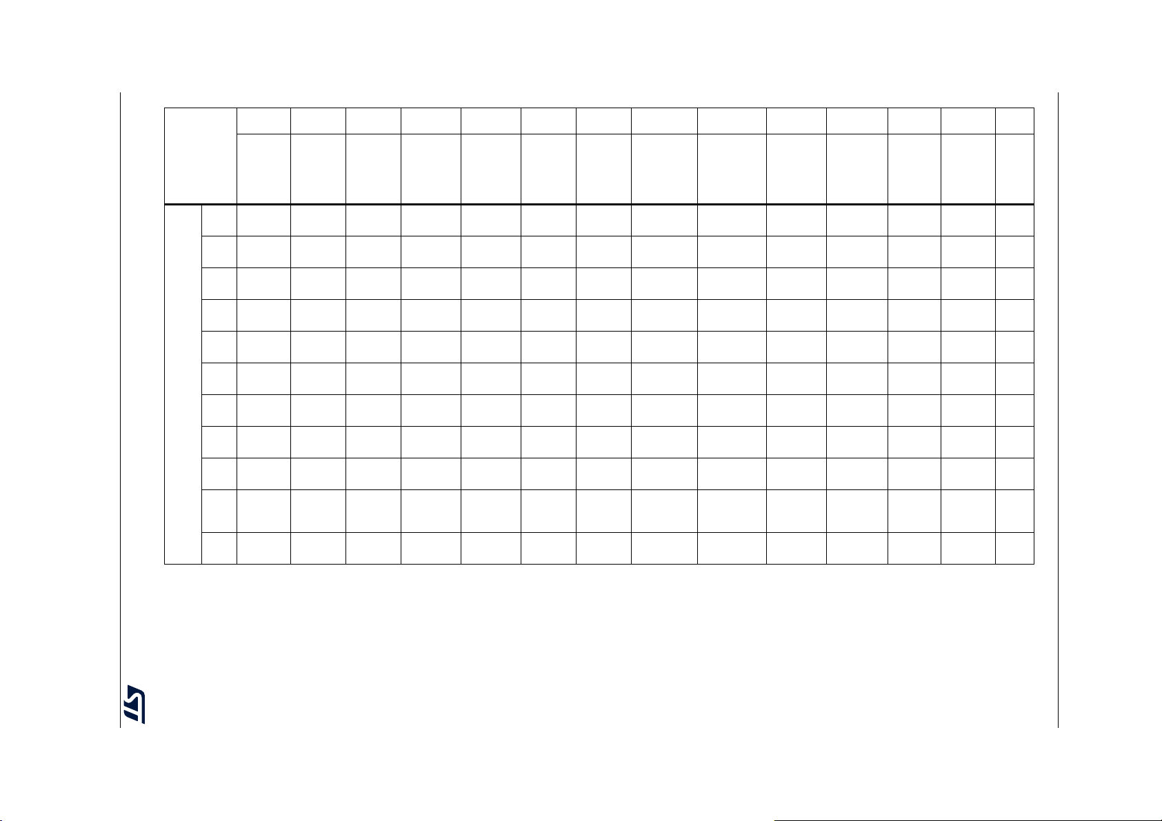
96/230 DS11853 Rev 7
Table 12. STM32F722xx and STM32F723xx alternate function mapping (continued)
AF0 AF1 AF2 AF3 AF4 AF5 AF6 AF7 AF8 AF9 AF10 AF11 AF12 AF15
Pinouts and pin description STM32F722xx STM32F723xx
Port
PG0--- - - -- - - - - -FMC_A10
PG1--- - - -- - - - - -FMC_A11
PG2--- - - -- - - - - -FMC_A12
PG3--- - - -- - - - - -FMC_A13
PG4--- - - -- - - - - -
PG5--- - - -- - - - - -
Port G
PG6--- - - -- - - - - --
PG7 - - - - - - - - USART6_CK - - - FMC_INT
PG8--- - - -- -
PG9 - - - - - - - - USART6_RX
PG10---- --- - - -SAI2_SD_B
SYS TIM1/2 TIM3/4/5
TIM8/9/10/1
1/LPTIM1
I2C1/2/3/U
SART1
SPI1/I2S1/
SPI2/I2S2/
SPI3/I2S3/
SPI4/5
SPI2/I2S2/
SPI3/I2S3/
SPI3/I2S3/
SAI1/
UART4
SPI2/I2S2/S
PI3/I2S3/US
ART1/2/3/UA
RT5
SAI2/USART
6/UART4/5/7/
8/OTG1_FS
USART6_RT
S
CAN1/TIM1
2/13/14/QU
ADSPI/
FMC/
OTG2_HS
QUADSPI_
BK2_IO2
SAI2/QUAD
SPI/SDMM
C2/OTG2_
HS/OTG1_
FS
---
SAI2_FS_B
SDMMC2
SDMMC2
_D0
SDMMC2
_D1
UART7/F
MC/SDM
OTG2_FS
FMC_A14/
FMC_BA0
FMC_A15/
FMC_BA1
FMC_SDCLKEVEN
FMC_NE2
/FMC_NC
FMC_NE3
MC1/
E
SYS
EVEN
TOUT
EVEN
TOUT
EVEN
TOUT
EVEN
TOUT
EVEN
TOUT
EVEN
TOUT
EVEN
TOUT
EVEN
TOUT
TOUT
EVEN
TOUT
EVEN
TOUT
Table 12. STM32F722xx and STM32F723xx alternate function mapping (continued)
AF0 AF1 AF2 AF3 AF4 AF5 AF6 AF7 AF8 AF9 AF10 AF11 AF12 AF15
STM32F722xx STM32F723xx Pinouts and pin description
DS11853 Rev 7 97/230
O
SPI2/I2S2/
SPI3/I2S3/
SPI3/I2S3/
SAI1/
UART4
SPI2/I2S2/S
PI3/I2S3/US
ART1/2/3/UA
RT5
-- - ---
SAI2/USART
6/UART4/5/7/
8/OTG1_FS
USART6_RT
S
USART6_CT
S
USART6_CT
S
Port
PG11---- --- - - -
PG12 - - -
Port G
PG13 TRACED0 - -
PG14 TRACED1 - -
PG15---- --- -
PH0--- - - -- - - - - --
PH1--- - - -- - - - - --
PH2 - - -
PH3--- - - -- - -
Port H
PH4 - - - - I2C2_SCL - - - - -
PH5 - - - - I2C2_SDA SPI5_NSS - - - - - -
PH6 - - - -
PH7 - - - - I2C3_SCL
SYS TIM1/2 TIM3/4/5
TIM8/9/10/1
1/LPTIM1
LPTIM1_IN
1
LPTIM1_O
UT
LPTIM1_ET
R
LPTIM1_IN
2
I2C1/2/3/U
SART1
I2C2_SMB
SPI1/I2S1/
SPI2/I2S2/
SPI3/I2S3/
SPI4/5
--- -
--- -
- - - - USART6_TX
--- - -
SPI5_SCK - - - TIM12_CH1 - -
A
SPI5_MIS
CAN1/TIM1
2/13/14/QU
ADSPI/
FMC/
OTG2_HS
QUADSPI_
BK2_IO3
QUADSPI_
BK2_IO0
QUADSPI_
BK2_IO1
SAI2/QUAD
SPI/SDMM
C2/OTG2_
HS/OTG1_
FS
SDMMC2_
D2
--
---FMC_A24
---
SAI2_SCK_
SAI2_MCK
_B
OTG_HS_U
LPI_NXT
SDMMC2
--
SDMMC2
_D3
--FMC_A25
B
-
-
--
UART7/F
MC/SDM
MC1/
OTG2_FS
FMC_NE4
FMC_SDN
CAS
FMC_SDC
KE0
FMC_SDNE0EVEN
FMC_SDNWEEVEN
FMC_SDNE1EVEN
FMC_SDC
KE1
SYS
EVEN
TOUT
EVEN
TOUT
EVEN
TOUT
EVEN
TOUT
EVEN
TOUT
EVEN
TOUT
EVEN
TOUT
EVEN
TOUT
TOUT
EVEN
TOUT
TOUT
TOUT
EVEN
TOUT
98/230 DS11853 Rev 7
Table 12. STM32F722xx and STM32F723xx alternate function mapping (continued)
AF0 AF1 AF2 AF3 AF4 AF5 AF6 AF7 AF8 AF9 AF10 AF11 AF12 AF15
Pinouts and pin description STM32F722xx STM32F723xx
Port
PH8 - - - - I2C3_SDA - - - - - - - FMC_D16
PH9 - - - -
PH10 - - TIM5_CH1 - - - - - - - - - FMC_D18
PH11 - - TIM5_CH2 - - - - - - - - - FMC_D19
Port H
PH12 - - TIM5_CH3 - - - - - - - - - FMC_D20
PH13 - - -
PH14 - - -
PH15 - - -
PI0 - - TIM5_CH4 - -
PI1 - - -
PI2 - - - TIM8_CH4 -
PI3 - - - TIM8_ETR -
Port I
PI4---TIM8_BKIN- -- - - -
PI5 - - - TIM8_CH1 - - - - - -
PI6 - - - TIM8_CH2 - - - - - - SAI2_SD_A - FMC_D28
SYS TIM1/2 TIM3/4/5
TIM8/9/10/1
1/LPTIM1
TIM8_CH1
N
TIM8_CH2
N
TIM8_CH3
N
TIM8_BKIN
2
I2C1/2/3/U
SART1
I2C3_SMB
SPI1/I2S1/
SPI2/I2S2/
SPI3/I2S3/
SPI4/5
A
- - - - UART4_TX CAN1_TX - - FMC_D21
- - - - UART4_RX CAN1_RX - - FMC_D22
- - - - - - - - FMC_D23
SPI2_NSS
/I2S2_WS
SPI2_SCK
/I2S2_CK
SPI2_MIS
SPI2_MO
SI/I2S2_S
SPI2/I2S2/
SPI3/I2S3/
SPI3/I2S3/
SAI1/
UART4
- - - - TIM12_CH2 - - FMC_D17
O
D
SPI2/I2S2/S
PI3/I2S3/US
ART1/2/3/UA
RT5
- - - - - - FMC_D24
- - - - - - FMC_D25
- - - - - - FMC_D26
- - - - - - FMC_D27
SAI2/USART
6/UART4/5/7/
8/OTG1_FS
CAN1/TIM1
2/13/14/QU
ADSPI/
FMC/
OTG2_HS
SAI2/QUAD
SPI/SDMM
C2/OTG2_
HS/OTG1_
FS
SAI2_MCK
_A
SAI2_SCK_
A
SDMMC2
UART7/F
MC/SDM
OTG2_FS
FMC_NBL2EVEN
-
FMC_NBL3EVEN
-
MC1/
SYS
EVEN
TOUT
EVEN
TOUT
EVEN
TOUT
EVEN
TOUT
EVEN
TOUT
EVEN
TOUT
EVEN
TOUT
EVEN
TOUT
EVEN
TOUT
EVEN
TOUT
EVEN
TOUT
EVEN
TOUT
TOUT
TOUT
EVEN
TOUT
Table 12. STM32F722xx and STM32F723xx alternate function mapping (continued)
AF0 AF1 AF2 AF3 AF4 AF5 AF6 AF7 AF8 AF9 AF10 AF11 AF12 AF15
STM32F722xx STM32F723xx Pinouts and pin description
DS11853 Rev 7 99/230
Port
PI7 - - - TIM8_CH3 - - - - - - SAI2_FS_A - FMC_D29
PI8--- - - -- - - - - --
PI9 - - - - - - - - UART4_RX CAN1_RX - - FMC_D30
PI10---- --- - - - --FMC_D31
Port I
PI11---- --- - - -
PI12---- --- - - - ---
PI13---- --- - - - ---
PI14---- --- - - - ---
PI15---- --- - - - ---
SYS TIM1/2 TIM3/4/5
TIM8/9/10/1
1/LPTIM1
I2C1/2/3/U
SART1
SPI1/I2S1/
SPI2/I2S2/
SPI3/I2S3/
SPI4/5
SPI2/I2S2/
SPI3/I2S3/
SPI3/I2S3/
SAI1/
UART4
SPI2/I2S2/S
PI3/I2S3/US
ART1/2/3/UA
RT5
SAI2/USART
6/UART4/5/7/
8/OTG1_FS
CAN1/TIM1
2/13/14/QU
ADSPI/
FMC/
OTG2_HS
SAI2/QUAD
SPI/SDMM
C2/OTG2_
HS/OTG1_
FS
OTG_HS_U
LPI_DIR
UART7/F
SDMMC2
MC/SDM
OTG2_FS
--
MC1/
SYS
EVEN
TOUT
EVEN
TOUT
EVEN
TOUT
EVEN
TOUT
EVEN
TOUT
EVEN
TOUT
EVEN
TOUT
EVEN
TOUT
EVEN
TOUT

Memory mapping STM32F722xx STM32F723xx
5 Memory mapping
Refer to the product line reference manual for details on the memory mapping as well as the
boundary addresses for all peripherals.
100/230 DS11853 Rev 7
 Loading...