

Datasheet STM32F479AI, STM32F479AG, STM32F479BI, STM32F479BG, STM32F479II Datasheet (STMicroelectronics)
...Page 1
STM32F479xx
WLCSP168
UFBGA176 (10 x 10 mm)
TFBGA216 (13 x 13 mm)
LQFP100 (14 × 14 mm)
LQFP144 (20 × 20 mm)
LQFP176 (24 × 24 mm)
LQFP208 (28 × 28 mm)
UFBGA169 (7 × 7 mm)
Arm®Cortex®-M4 32b MCU+FPU, 225DMIPS, up to 2MB Flash/384+4KB RAM, USB OTG HS/FS,
Ethernet, FMC, dual Quad-SPI, Crypto, Graphical accelerator, Camera IF, LCD-TFT & MIPI DSI
Datasheet - production data
Features
Core: Arm® 32-bit Cortex®-M4 CPU with FPU,
Adaptive real-time accelerator (ART
Accelerator™) allowing 0-wait state execution
from Flash memory, frequency up to 180 MHz,
MPU, 225 DMIPS/1.25 DMIPS/MHz (Dhrystone
2.1), and DSP instructions
Memories
– Up to 2 MB of Flash memory organized into
two banks allowing read-while-write
– Up to 384+4 KB of SRAM including 64 KB of
CCM (core coupled memory) data RAM
– Flexible external memory controller with up
to 32-bit data bus: SRAM, PSRAM,
SDRAM/LPSDR, SDRAM, Flash
NOR/NAND memories
– Dual-flash mode Quad-SPI interface
Graphics:
– Chrom-ART Accelerator™ (DMA2D),
graphical hardware accelerator enabling
enhanced graphical user interface with
minimum CPU load
– LCD parallel interface, 8080/6800 modes
– LCD TFT controller supporting up to XGA
resolution
–MIPI
®
DSI host controller supporting up to
720p 30Hz resolution
Clock, reset and supply management
– 1.7 V to 3.6 V application supply and I/Os
– POR, PDR, PVD and BOR
– 4-to-26 MHz crystal oscillator
– Internal 16 MHz factory-trimmed RC (1%
accuracy)
– 32 kHz oscillator for RTC with calibration
– Internal 32 kHz RC with calibration
Low power
– Sleep, Stop and Standby modes
–V
supply for RTC, 20×32 bit backup
BAT
registers + optional 4 KB backup SRAM
3×12-bit, 2.4 MSPS ADC: up to 24 channels and
7.2 MSPS in triple interleaved mode
2×12-bit D/A converters
General-purpose DMA: 16-stream DMA
controller with FIFOs and burst support
Up to 17 timers: up to twelve 16-bit and two 32-
bit timers up to 180 MHz, each with up to 4
IC/OC/PWM or pulse counter and quadrature
(incremental) encoder input. 2x watchdogs and
SysTick timer
Debug mode
– SWD & JTAG interfaces
–Cortex
®
-M4 Trace Macrocell™
Up to 161 I/O ports with interrupt capability
– Up to 157 fast I/Os up to 90 MHz
– Up to 159 5 V-tolerant I/Os
Up to 21 communication interfaces
– Up to 3 × I
2
C interfaces (SMBus/PMBus)
– Up to 4 USARTs and 4 UARTs (11.25 Mbit/s,
ISO7816 interface, LIN, IrDA, modem
control)
– Up to 6 SPIs (45 Mbits/s), 2 with muxed full-
duplex I
2
S for audio class accuracy via
internal audio PLL or external clock
– 1 x SAI (serial audio interface)
– 2 × CAN (2.0B Active)
–SDIO interface
Advanced connectivity
– USB 2.0 full-speed device/host/OTG
controller with on-chip PHY
– USB 2.0 high-speed/full-speed
device/host/OTG controller with dedicated
DMA, on-chip full-speed PHY and ULPI
– Dedicated USB power rail enabling on-chip
PHYs operation throughout the entire MCU
power supply range
– 10/100 Ethernet MAC with dedicated DMA:
supports IEEE 1588v2 hardware, MII/RMII
8- to 14-bit parallel camera interface up to
54 Mbytes/s
Cryptographic accelerator
– HW accelerator for AES 128, 192, 256,
Triple DES, HASH (MD5, SHA-1, SHA-2)
and HMAC
True random number generator
CRC calculation unit
RTC: subsecond accuracy, hardware calendar
96-bit unique ID
Reference Part numbers
STM32F479xx
Table 1. Device summary
STM32F479AI, STM32F479AG, STM32F479BI,
STM32F479BG, STM32F479II, STM32F479IG,
STM32F479NI, STM32F479NG, STM32479VG,
STM32479VI, STM32479ZG, STM32479ZI
Jan u ar y 2 021 DS 1111 8 Rev 6 1/ 220
This is information on a product in full production.
www.st.com
Page 2

Contents STM32F479xx
Contents
1 Description . . . . . . . . . . . . . . . . . . . . . . . . . . . . . . . . . . . . . . . . . . . . . . . . 12
1.1 Compatibility throughout the family . . . . . . . . . . . . . . . . . . . . . . . . . . . . . 15
1.1.1 LQFP176 package . . . . . . . . . . . . . . . . . . . . . . . . . . . . . . . . . . . . . . . . . 16
1.1.2 LQFP208 package . . . . . . . . . . . . . . . . . . . . . . . . . . . . . . . . . . . . . . . . . 17
1.1.3 UFBGA176 package . . . . . . . . . . . . . . . . . . . . . . . . . . . . . . . . . . . . . . . 18
1.1.4 TFBGA216 package . . . . . . . . . . . . . . . . . . . . . . . . . . . . . . . . . . . . . . . 19
2 Functional overview . . . . . . . . . . . . . . . . . . . . . . . . . . . . . . . . . . . . . . . . 21
2.1 Arm® Cortex®-M4 with FPU and embedded Flash and SRAM . . . . . . . . 21
2.2 Adaptive real-time memory accelerator (ART Accelerator™) . . . . . . . . . 21
2.3 Memory protection unit . . . . . . . . . . . . . . . . . . . . . . . . . . . . . . . . . . . . . . . 21
2.4 Embedded Flash memory . . . . . . . . . . . . . . . . . . . . . . . . . . . . . . . . . . . . 22
2.5 CRC (cyclic redundancy check) calculation unit . . . . . . . . . . . . . . . . . . . 22
2.6 Embedded SRAM . . . . . . . . . . . . . . . . . . . . . . . . . . . . . . . . . . . . . . . . . . . 22
2.7 Multi-AHB bus matrix . . . . . . . . . . . . . . . . . . . . . . . . . . . . . . . . . . . . . . . . 22
2.8 DMA controller (DMA) . . . . . . . . . . . . . . . . . . . . . . . . . . . . . . . . . . . . . . . 23
2.9 Flexible memory controller (FMC) . . . . . . . . . . . . . . . . . . . . . . . . . . . . . . 24
2.10 Quad-SPI memory interface (QUADSPI) . . . . . . . . . . . . . . . . . . . . . . . . . 25
2.11 LCD-TFT controller . . . . . . . . . . . . . . . . . . . . . . . . . . . . . . . . . . . . . . . . . . 25
2.12 DSI Host (DSIHOST) . . . . . . . . . . . . . . . . . . . . . . . . . . . . . . . . . . . . . . . . 25
2.13 Chrom-ART Accelerator™ (DMA2D) . . . . . . . . . . . . . . . . . . . . . . . . . . . . 27
2.14 Nested vectored interrupt controller (NVIC) . . . . . . . . . . . . . . . . . . . . . . . 27
2.15 External interrupt/event controller (EXTI) . . . . . . . . . . . . . . . . . . . . . . . . . 27
2.16 Clocks and startup . . . . . . . . . . . . . . . . . . . . . . . . . . . . . . . . . . . . . . . . . . 28
2.17 Boot modes . . . . . . . . . . . . . . . . . . . . . . . . . . . . . . . . . . . . . . . . . . . . . . . 28
2.18 Power supply schemes . . . . . . . . . . . . . . . . . . . . . . . . . . . . . . . . . . . . . . 28
2.19 Power supply supervisor . . . . . . . . . . . . . . . . . . . . . . . . . . . . . . . . . . . . . 30
2.19.1 Internal reset ON . . . . . . . . . . . . . . . . . . . . . . . . . . . . . . . . . . . . . . . . . . 30
2.19.2 Internal reset OFF . . . . . . . . . . . . . . . . . . . . . . . . . . . . . . . . . . . . . . . . . 30
2.20 Voltage regulator . . . . . . . . . . . . . . . . . . . . . . . . . . . . . . . . . . . . . . . . . . . 31
2.20.1 Regulator ON . . . . . . . . . . . . . . . . . . . . . . . . . . . . . . . . . . . . . . . . . . . . . 32
2.20.2 Regulator OFF . . . . . . . . . . . . . . . . . . . . . . . . . . . . . . . . . . . . . . . . . . . . 33
2/22 0 D S 1111 8 R e v 6
Page 3

STM32F479xx Contents
2.20.3 Regulator ON/OFF and internal reset ON/OFF availability . . . . . . . . . . 35
2.21 Real-time clock (RTC), backup SRAM and backup registers . . . . . . . . . . 35
2.22 Low-power modes . . . . . . . . . . . . . . . . . . . . . . . . . . . . . . . . . . . . . . . . . . 36
2.23 V
operation . . . . . . . . . . . . . . . . . . . . . . . . . . . . . . . . . . . . . . . . . . . . . 37
BAT
2.24 Timers and watchdogs . . . . . . . . . . . . . . . . . . . . . . . . . . . . . . . . . . . . . . . 37
2.24.1 Advanced-control timers (TIM1, TIM8) . . . . . . . . . . . . . . . . . . . . . . . . . 38
2.24.2 General-purpose timers (TIMx) . . . . . . . . . . . . . . . . . . . . . . . . . . . . . . . 39
2.24.3 Basic timers TIM6 and TIM7 . . . . . . . . . . . . . . . . . . . . . . . . . . . . . . . . . 39
2.24.4 Independent watchdog . . . . . . . . . . . . . . . . . . . . . . . . . . . . . . . . . . . . . 39
2.24.5 Window watchdog . . . . . . . . . . . . . . . . . . . . . . . . . . . . . . . . . . . . . . . . . 39
2.24.6 SysTick timer . . . . . . . . . . . . . . . . . . . . . . . . . . . . . . . . . . . . . . . . . . . . . 40
2.25 Inter-integrated circuit interface (I2C) . . . . . . . . . . . . . . . . . . . . . . . . . . . . 40
2.26 Universal synchronous/asynchronous receiver transmitters (USART) . . 40
2.27 Serial peripheral interface (SPI) . . . . . . . . . . . . . . . . . . . . . . . . . . . . . . . . 41
2.28 Inter-integrated sound (I
2
S) . . . . . . . . . . . . . . . . . . . . . . . . . . . . . . . . . . . 41
2.29 Serial Audio interface (SAI1) . . . . . . . . . . . . . . . . . . . . . . . . . . . . . . . . . . 42
2.30 Audio PLL (PLLI2S) . . . . . . . . . . . . . . . . . . . . . . . . . . . . . . . . . . . . . . . . . 42
2.31 Audio and LCD PLL(PLLSAI) . . . . . . . . . . . . . . . . . . . . . . . . . . . . . . . . . . 42
2.32 Secure digital input/output interface (SDIO) . . . . . . . . . . . . . . . . . . . . . . . 42
2.33 Ethernet MAC interface with dedicated DMA and IEEE 1588 support . . . 43
2.34 Controller area network (bxCAN) . . . . . . . . . . . . . . . . . . . . . . . . . . . . . . . 43
2.35 Universal serial bus on-the-go full-speed (OTG_FS) . . . . . . . . . . . . . . . . 44
2.36 Universal serial bus on-the-go high-speed (OTG_HS) . . . . . . . . . . . . . . . 44
2.37 Digital camera interface (DCMI) . . . . . . . . . . . . . . . . . . . . . . . . . . . . . . . . 45
2.38 Cryptographic accelerator . . . . . . . . . . . . . . . . . . . . . . . . . . . . . . . . . . . . 45
2.39 Random number generator (RNG) . . . . . . . . . . . . . . . . . . . . . . . . . . . . . . 45
2.40 General-purpose input/outputs (GPIOs) . . . . . . . . . . . . . . . . . . . . . . . . . . 45
2.41 Analog-to-digital converters (ADCs) . . . . . . . . . . . . . . . . . . . . . . . . . . . . . 46
2.42 Temperature sensor . . . . . . . . . . . . . . . . . . . . . . . . . . . . . . . . . . . . . . . . . 46
2.43 Digital-to-analog converter (DAC) . . . . . . . . . . . . . . . . . . . . . . . . . . . . . . 46
2.44 Serial wire JTAG debug port (SWJ-DP) . . . . . . . . . . . . . . . . . . . . . . . . . . 47
2.45 Embedded Trace Macrocell™ . . . . . . . . . . . . . . . . . . . . . . . . . . . . . . . . . 47
3 Pinouts and pin description . . . . . . . . . . . . . . . . . . . . . . . . . . . . . . . . . . 48
DS 1111 8 Rev 6 3/ 2 2 0
5
Page 4

Contents STM32F479xx
4 Memory mapping . . . . . . . . . . . . . . . . . . . . . . . . . . . . . . . . . . . . . . . . . . . 84
5 Electrical characteristics . . . . . . . . . . . . . . . . . . . . . . . . . . . . . . . . . . . . 89
5.1 Parameter conditions . . . . . . . . . . . . . . . . . . . . . . . . . . . . . . . . . . . . . . . . 89
5.1.1 Minimum and maximum values . . . . . . . . . . . . . . . . . . . . . . . . . . . . . . . 89
5.1.2 Typical values . . . . . . . . . . . . . . . . . . . . . . . . . . . . . . . . . . . . . . . . . . . . 89
5.1.3 Typical curves . . . . . . . . . . . . . . . . . . . . . . . . . . . . . . . . . . . . . . . . . . . . 89
5.1.4 Loading capacitor . . . . . . . . . . . . . . . . . . . . . . . . . . . . . . . . . . . . . . . . . 89
5.1.5 Pin input voltage . . . . . . . . . . . . . . . . . . . . . . . . . . . . . . . . . . . . . . . . . . 89
5.1.6 Power supply scheme . . . . . . . . . . . . . . . . . . . . . . . . . . . . . . . . . . . . . . 90
5.1.7 Current consumption measurement . . . . . . . . . . . . . . . . . . . . . . . . . . . 91
5.2 Absolute maximum ratings . . . . . . . . . . . . . . . . . . . . . . . . . . . . . . . . . . . . 91
5.3 Operating conditions . . . . . . . . . . . . . . . . . . . . . . . . . . . . . . . . . . . . . . . . 93
5.3.1 General operating conditions . . . . . . . . . . . . . . . . . . . . . . . . . . . . . . . . . 93
5.3.2 VCAP1/VCAP2 external capacitor . . . . . . . . . . . . . . . . . . . . . . . . . . . . . 95
5.3.3 Operating conditions at power-up / power-down (regulator ON) . . . . . . 96
5.3.4 Operating conditions at power-up / power-down (regulator OFF) . . . . . 96
5.3.5 Reset and power control block characteristics . . . . . . . . . . . . . . . . . . . 96
5.3.6 Over-drive switching characteristics . . . . . . . . . . . . . . . . . . . . . . . . . . . 98
5.3.7 Supply current characteristics . . . . . . . . . . . . . . . . . . . . . . . . . . . . . . . . 98
5.3.8 Wakeup time from low-power modes . . . . . . . . . . . . . . . . . . . . . . . . . . 114
5.3.9 External clock source characteristics . . . . . . . . . . . . . . . . . . . . . . . . . . 115
5.3.10 Internal clock source characteristics . . . . . . . . . . . . . . . . . . . . . . . . . . 119
5.3.11 PLL characteristics . . . . . . . . . . . . . . . . . . . . . . . . . . . . . . . . . . . . . . . . 120
5.3.12 PLL spread spectrum clock generation (SSCG) characteristics . . . . . 123
5.3.13 MIPI D-PHY characteristics . . . . . . . . . . . . . . . . . . . . . . . . . . . . . . . . . 124
5.3.14 MIPI D-PHY PLL characteristics . . . . . . . . . . . . . . . . . . . . . . . . . . . . . 127
5.3.15 MIPI D-PHY regulator characteristics . . . . . . . . . . . . . . . . . . . . . . . . . 128
5.3.16 Memory characteristics . . . . . . . . . . . . . . . . . . . . . . . . . . . . . . . . . . . . 129
5.3.17 EMC characteristics . . . . . . . . . . . . . . . . . . . . . . . . . . . . . . . . . . . . . . . 131
5.3.18 Absolute maximum ratings (electrical sensitivity) . . . . . . . . . . . . . . . . 132
5.3.19 I/O current injection characteristics . . . . . . . . . . . . . . . . . . . . . . . . . . . 133
5.3.20 I/O port characteristics . . . . . . . . . . . . . . . . . . . . . . . . . . . . . . . . . . . . . 134
5.3.21 NRST pin characteristics . . . . . . . . . . . . . . . . . . . . . . . . . . . . . . . . . . . 140
5.3.22 TIM timer characteristics . . . . . . . . . . . . . . . . . . . . . . . . . . . . . . . . . . . 141
5.3.23 Communications interfaces . . . . . . . . . . . . . . . . . . . . . . . . . . . . . . . . . 141
5.3.24 12-bit ADC characteristics . . . . . . . . . . . . . . . . . . . . . . . . . . . . . . . . . . 156
4/22 0 D S 1111 8 R e v 6
Page 5

STM32F479xx Contents
5.3.25 Temperature sensor characteristics . . . . . . . . . . . . . . . . . . . . . . . . . . . 162
5.3.26 V
5.3.27 Reference voltage . . . . . . . . . . . . . . . . . . . . . . . . . . . . . . . . . . . . . . . . 162
5.3.28 DAC electrical characteristics . . . . . . . . . . . . . . . . . . . . . . . . . . . . . . . 163
5.3.29 FMC characteristics . . . . . . . . . . . . . . . . . . . . . . . . . . . . . . . . . . . . . . . 165
5.3.30 Quad-SPI interface characteristics . . . . . . . . . . . . . . . . . . . . . . . . . . . 185
5.3.31 Camera interface (DCMI) timing specifications . . . . . . . . . . . . . . . . . . 186
5.3.32 LCD-TFT controller (LTDC) characteristics . . . . . . . . . . . . . . . . . . . . . 187
5.3.33 SD/SDIO MMC card host interface (SDIO) characteristics . . . . . . . . . 189
5.3.34 RTC characteristics . . . . . . . . . . . . . . . . . . . . . . . . . . . . . . . . . . . . . . . 191
monitoring characteristics . . . . . . . . . . . . . . . . . . . . . . . . . . . . . . 162
BAT
6 Package information . . . . . . . . . . . . . . . . . . . . . . . . . . . . . . . . . . . . . . . 192
6.1 LQFP100 package information . . . . . . . . . . . . . . . . . . . . . . . . . . . . . . . . 192
6.2 LQFP144 package information . . . . . . . . . . . . . . . . . . . . . . . . . . . . . . . . 195
6.3 WLCSP168 package information . . . . . . . . . . . . . . . . . . . . . . . . . . . . . . 198
6.4 UFBGA169 package information . . . . . . . . . . . . . . . . . . . . . . . . . . . . . . 200
6.5 LQFP176 package information . . . . . . . . . . . . . . . . . . . . . . . . . . . . . . . . 203
6.6 UFBGA(176+25) package information . . . . . . . . . . . . . . . . . . . . . . . . . . 207
6.7 LQFP208 package information . . . . . . . . . . . . . . . . . . . . . . . . . . . . . . . . 208
6.8 TFBGA216 package information . . . . . . . . . . . . . . . . . . . . . . . . . . . . . . 212
6.9 Thermal characteristics . . . . . . . . . . . . . . . . . . . . . . . . . . . . . . . . . . . . . 215
7 Part numbering . . . . . . . . . . . . . . . . . . . . . . . . . . . . . . . . . . . . . . . . . . . 216
Appendix A Recommendations when using internal reset OFF . . . . . . . . . . . 217
A.1 Operating conditions . . . . . . . . . . . . . . . . . . . . . . . . . . . . . . . . . . . . . . . . 217
Revision history . . . . . . . . . . . . . . . . . . . . . . . . . . . . . . . . . . . . . . . . . . . . . . . . . . . 218
DS 1111 8 Rev 6 5/ 2 2 0
5
Page 6

List of tables STM32F479xx
List of tables
Table 1. Device summary . . . . . . . . . . . . . . . . . . . . . . . . . . . . . . . . . . . . . . . . . . . . . . . . . . . . . . . . . . 1
Table 2. STM32F479xx features and peripheral counts. . . . . . . . . . . . . . . . . . . . . . . . . . . . . . . . . . 13
Table 3. Voltage regulator configuration mode versus device operating mode . . . . . . . . . . . . . . . . 32
Table 4. Regulator ON/OFF and internal reset ON/OFF availability. . . . . . . . . . . . . . . . . . . . . . . . . 35
Table 5. Voltage regulator modes in stop mode . . . . . . . . . . . . . . . . . . . . . . . . . . . . . . . . . . . . . . . . 36
Table 6. Timer feature comparison . . . . . . . . . . . . . . . . . . . . . . . . . . . . . . . . . . . . . . . . . . . . . . . . . . 38
Table 7. Comparison of I2C analog and digital filters . . . . . . . . . . . . . . . . . . . . . . . . . . . . . . . . . . . . 40
Table 8. USART feature comparison . . . . . . . . . . . . . . . . . . . . . . . . . . . . . . . . . . . . . . . . . . . . . . . . 41
Table 9. Legend/abbreviations used in the pinout table . . . . . . . . . . . . . . . . . . . . . . . . . . . . . . . . . . 56
Table 10. STM32F479xx pin and ball definitions . . . . . . . . . . . . . . . . . . . . . . . . . . . . . . . . . . . . . . . . 57
Table 11. FMC pin definition . . . . . . . . . . . . . . . . . . . . . . . . . . . . . . . . . . . . . . . . . . . . . . . . . . . . . . . . 71
Table 12. Alternate function . . . . . . . . . . . . . . . . . . . . . . . . . . . . . . . . . . . . . . . . . . . . . . . . . . . . . . . . 74
Table 13. STM32F479xx register boundary addresses . . . . . . . . . . . . . . . . . . . . . . . . . . . . . . . . . . . 85
Table 14. Voltage characteristics . . . . . . . . . . . . . . . . . . . . . . . . . . . . . . . . . . . . . . . . . . . . . . . . . . . . 91
Table 15. Current characteristics . . . . . . . . . . . . . . . . . . . . . . . . . . . . . . . . . . . . . . . . . . . . . . . . . . . . 92
Table 16. Thermal characteristics. . . . . . . . . . . . . . . . . . . . . . . . . . . . . . . . . . . . . . . . . . . . . . . . . . . . 92
Table 17. General operating conditions . . . . . . . . . . . . . . . . . . . . . . . . . . . . . . . . . . . . . . . . . . . . . . . 93
Table 18. Limitations depending on the operating power supply range . . . . . . . . . . . . . . . . . . . . . . . 95
Table 19. VCAP1/VCAP2 operating conditions . . . . . . . . . . . . . . . . . . . . . . . . . . . . . . . . . . . . . . . . . 96
Table 20. Operating conditions at power-up / power-down (regulator ON) . . . . . . . . . . . . . . . . . . . . 96
Table 21. Operating conditions at power-up / power-down (regulator OFF). . . . . . . . . . . . . . . . . . . . 96
Table 22. Reset and power control block characteristics . . . . . . . . . . . . . . . . . . . . . . . . . . . . . . . . . 97
Table 23. Over-drive switching characteristics . . . . . . . . . . . . . . . . . . . . . . . . . . . . . . . . . . . . . . . . . . 98
Table 24. Typical and maximum current consumption in Run mode, code with data processing
running from Flash memory (ART accelerator enabled except prefetch) or RAM,
regulator ON . . . . . . . . . . . . . . . . . . . . . . . . . . . . . . . . . . . . . . . . . . . . . . . . . . . . . . . . . . . 100
Table 25. Typical and maximum current consumption in Run mode, code with data processing
running from Flash memory (ART accelerator disabled), regulator ON . . . . . . . . . . . . . . 101
Table 26. Typical and maximum current consumption in Run mode, code with data
processing running from Flash memory (ART accelerator enabled except prefetch),
regulator OFF . . . . . . . . . . . . . . . . . . . . . . . . . . . . . . . . . . . . . . . . . . . . . . . . . . . . . . . . . . 102
Table 27. Typical and maximum current consumption in Sleep mode, regulator ON . . . . . . . . . . . . 103
Table 28. Typical and maximum current consumption in Sleep mode, regulator OFF . . . . . . . . . . . 104
Table 29. Typical and maximum current consumption in Stop mode . . . . . . . . . . . . . . . . . . . . . . . . 105
Table 30. Typical and maximum current consumption in Standby mode . . . . . . . . . . . . . . . . . . . . . 106
Table 31. Typical and maximum current consumption in V
Table 32. Switching output I/O current consumption . . . . . . . . . . . . . . . . . . . . . . . . . . . . . . . . . . . . 109
Table 33. Peripheral current consumption . . . . . . . . . . . . . . . . . . . . . . . . . . . . . . . . . . . . . . . . . . . . 111
Table 34. Low-power mode wakeup timings . . . . . . . . . . . . . . . . . . . . . . . . . . . . . . . . . . . . . . . . . . 114
Table 35. High-speed external user clock characteristics. . . . . . . . . . . . . . . . . . . . . . . . . . . . . . . . . 115
Table 36. Low-speed external user clock characteristics . . . . . . . . . . . . . . . . . . . . . . . . . . . . . . . . . 115
Table 37. HSE 4-26 MHz oscillator characteristics . . . . . . . . . . . . . . . . . . . . . . . . . . . . . . . . . . . . . 117
Table 38. LSE oscillator characteristics (f
Table 39. HSI oscillator characteristics . . . . . . . . . . . . . . . . . . . . . . . . . . . . . . . . . . . . . . . . . . . . . . 119
Table 40. LSI oscillator characteristics . . . . . . . . . . . . . . . . . . . . . . . . . . . . . . . . . . . . . . . . . . . . . . 120
Table 41. Main PLL characteristics. . . . . . . . . . . . . . . . . . . . . . . . . . . . . . . . . . . . . . . . . . . . . . . . . . 120
Table 42. PLLI2S (audio PLL) characteristics . . . . . . . . . . . . . . . . . . . . . . . . . . . . . . . . . . . . . . . . . 121
Table 43. PLLSAI (audio and LCD-TFT PLL) characteristics . . . . . . . . . . . . . . . . . . . . . . . . . . . . . . 122
= 32.768 kHz) . . . . . . . . . . . . . . . . . . . . . . . . . . . . . . 118
LSE
mode. . . . . . . . . . . . . . . . . . . . . . . . 107
BAT
6/22 0 D S 1111 8 R e v 6
Page 7

STM32F479xx List of tables
Table 44. SSCG parameters constraint . . . . . . . . . . . . . . . . . . . . . . . . . . . . . . . . . . . . . . . . . . . . . . 123
Table 45. MIPI D-PHY characteristics . . . . . . . . . . . . . . . . . . . . . . . . . . . . . . . . . . . . . . . . . . . . . . . 124
Table 46. MIPI D-PHY AC characteristics LP mode and HS/LP transitions . . . . . . . . . . . . . . . . . . . 126
Table 47. DSI-PLL characteristics . . . . . . . . . . . . . . . . . . . . . . . . . . . . . . . . . . . . . . . . . . . . . . . . . . 127
Table 48. DSI regulator characteristics. . . . . . . . . . . . . . . . . . . . . . . . . . . . . . . . . . . . . . . . . . . . . . . 128
Table 49. Flash memory characteristics . . . . . . . . . . . . . . . . . . . . . . . . . . . . . . . . . . . . . . . . . . . . . . 129
Table 50. Flash memory programming . . . . . . . . . . . . . . . . . . . . . . . . . . . . . . . . . . . . . . . . . . . . . . . 129
Table 51. Flash memory programming with V
PP . . . . . . . . . . . . . . . . . . . . . . . . . . . . . . . . . . . . . . . . . . . . . . . . . . 130
Table 52. Flash memory endurance and data retention . . . . . . . . . . . . . . . . . . . . . . . . . . . . . . . . . . 131
Table 53. EMS characteristics . . . . . . . . . . . . . . . . . . . . . . . . . . . . . . . . . . . . . . . . . . . . . . . . . . . . . 131
Table 54. EMI characteristics . . . . . . . . . . . . . . . . . . . . . . . . . . . . . . . . . . . . . . . . . . . . . . . . . . . . . . 132
Table 55. ESD absolute maximum ratings . . . . . . . . . . . . . . . . . . . . . . . . . . . . . . . . . . . . . . . . . . . . 133
Table 56. Electrical sensitivities . . . . . . . . . . . . . . . . . . . . . . . . . . . . . . . . . . . . . . . . . . . . . . . . . . . . 133
Table 57. I/O current injection susceptibility . . . . . . . . . . . . . . . . . . . . . . . . . . . . . . . . . . . . . . . . . . . 134
Table 58. I/O static characteristics . . . . . . . . . . . . . . . . . . . . . . . . . . . . . . . . . . . . . . . . . . . . . . . . . . 134
Table 59. Output voltage characteristics . . . . . . . . . . . . . . . . . . . . . . . . . . . . . . . . . . . . . . . . . . . . . 137
Table 60. I/O AC characteristics . . . . . . . . . . . . . . . . . . . . . . . . . . . . . . . . . . . . . . . . . . . . . . . . . . . . 138
Table 61. NRST pin characteristics . . . . . . . . . . . . . . . . . . . . . . . . . . . . . . . . . . . . . . . . . . . . . . . . . 140
Table 62. TIMx characteristics . . . . . . . . . . . . . . . . . . . . . . . . . . . . . . . . . . . . . . . . . . . . . . . . . . . . . 141
Table 63. I2C analog filter characteristics. . . . . . . . . . . . . . . . . . . . . . . . . . . . . . . . . . . . . . . . . . . . . 141
Table 64. SPI dynamic characteristics . . . . . . . . . . . . . . . . . . . . . . . . . . . . . . . . . . . . . . . . . . . . . . . 142
Table 65. I
2
S dynamic characteristics . . . . . . . . . . . . . . . . . . . . . . . . . . . . . . . . . . . . . . . . . . . . . . . 146
Table 66. SAI characteristics . . . . . . . . . . . . . . . . . . . . . . . . . . . . . . . . . . . . . . . . . . . . . . . . . . . . . . 148
Table 67. USB OTG full speed startup time . . . . . . . . . . . . . . . . . . . . . . . . . . . . . . . . . . . . . . . . . . . 150
Table 68. USB OTG full speed DC electrical characteristics . . . . . . . . . . . . . . . . . . . . . . . . . . . . . . 150
Table 69. USB OTG full speed electrical characteristics . . . . . . . . . . . . . . . . . . . . . . . . . . . . . . . . . 151
Table 70. USB HS DC electrical characteristics . . . . . . . . . . . . . . . . . . . . . . . . . . . . . . . . . . . . . . . . 151
Table 71. USB HS clock timing parameters . . . . . . . . . . . . . . . . . . . . . . . . . . . . . . . . . . . . . . . . . . . 152
Table 72. Dynamic characteristics: USB ULPI . . . . . . . . . . . . . . . . . . . . . . . . . . . . . . . . . . . . . . . . . 153
Table 73. Dynamics characteristics: Ethernet MAC signals for SMI. . . . . . . . . . . . . . . . . . . . . . . . . 154
Table 74. Dynamics characteristics: Ethernet MAC signals for RMII . . . . . . . . . . . . . . . . . . . . . . . . 155
Table 75. Dynamics characteristics: Ethernet MAC signals for MII . . . . . . . . . . . . . . . . . . . . . . . . . 155
Table 76. ADC characteristics . . . . . . . . . . . . . . . . . . . . . . . . . . . . . . . . . . . . . . . . . . . . . . . . . . . . . 156
Table 77. ADC static accuracy at f
Table 78. ADC static accuracy at f
Table 79. ADC static accuracy at f
Table 80. ADC dynamic accuracy at f
Table 81. ADC dynamic accuracy at f
= 18 MHz . . . . . . . . . . . . . . . . . . . . . . . . . . . . . . . . . . . . . . . 158
ADC
= 30 MHz . . . . . . . . . . . . . . . . . . . . . . . . . . . . . . . . . . . . . . . 158
ADC
= 36 MHz . . . . . . . . . . . . . . . . . . . . . . . . . . . . . . . . . . . . . . . 158
ADC
= 18 MHz - limited test conditions . . . . . . . . . . . . . . . . . 159
ADC
= 36 MHz - limited test conditions . . . . . . . . . . . . . . . . . 159
ADC
Table 82. Temperature sensor characteristics . . . . . . . . . . . . . . . . . . . . . . . . . . . . . . . . . . . . . . . . . 162
Table 83. Temperature sensor calibration values. . . . . . . . . . . . . . . . . . . . . . . . . . . . . . . . . . . . . . . 162
Table 84. V
monitoring characteristics . . . . . . . . . . . . . . . . . . . . . . . . . . . . . . . . . . . . . . . . . . . . 162
BAT
Table 85. internal reference voltage . . . . . . . . . . . . . . . . . . . . . . . . . . . . . . . . . . . . . . . . . . . . . . . . 162
Table 86. Internal reference voltage calibration values . . . . . . . . . . . . . . . . . . . . . . . . . . . . . . . . . . 163
Table 87. DAC characteristics . . . . . . . . . . . . . . . . . . . . . . . . . . . . . . . . . . . . . . . . . . . . . . . . . . . . . 163
Table 88. Asynchronous non-multiplexed SRAM/PSRAM/NOR - read timings . . . . . . . . . . . . . . . . 167
Table 89. Asynchronous non-multiplexed SRAM/PSRAM/NOR read - NWAIT timings . . . . . . . . . . 167
Table 90. Asynchronous non-multiplexed SRAM/PSRAM/NOR write timings . . . . . . . . . . . . . . . . . 168
Table 91. Asynchronous non-multiplexed SRAM/PSRAM/NOR write - NWAIT timings . . . . . . . . . . 169
Table 92. Asynchronous multiplexed PSRAM/NOR read timings. . . . . . . . . . . . . . . . . . . . . . . . . . . 170
Table 93. Asynchronous multiplexed PSRAM/NOR read-NWAIT timings . . . . . . . . . . . . . . . . . . . . 170
Table 94. Asynchronous multiplexed PSRAM/NOR write timings . . . . . . . . . . . . . . . . . . . . . . . . . . 171
Table 95. Asynchronous multiplexed PSRAM/NOR write-NWAIT timings . . . . . . . . . . . . . . . . . . . . 172
DS 1111 8 Rev 6 7/ 2 2 0
8
Page 8

List of tables STM32F479xx
Table 96. Synchronous multiplexed NOR/PSRAM read timings . . . . . . . . . . . . . . . . . . . . . . . . . . . 174
Table 97. Synchronous multiplexed PSRAM write timings . . . . . . . . . . . . . . . . . . . . . . . . . . . . . . . . 176
Table 98. Synchronous non-multiplexed NOR/PSRAM read timings . . . . . . . . . . . . . . . . . . . . . . . . 177
Table 99. Synchronous non-multiplexed PSRAM write timings . . . . . . . . . . . . . . . . . . . . . . . . . . . . 178
Table 100. Switching characteristics for NAND Flash read cycles . . . . . . . . . . . . . . . . . . . . . . . . . . . 181
Table 101. Switching characteristics for NAND Flash write cycles. . . . . . . . . . . . . . . . . . . . . . . . . . . 181
Table 102. SDRAM read timings . . . . . . . . . . . . . . . . . . . . . . . . . . . . . . . . . . . . . . . . . . . . . . . . . . . . 182
Table 103. LPSDR SDRAM read timings . . . . . . . . . . . . . . . . . . . . . . . . . . . . . . . . . . . . . . . . . . . . . . 183
Table 104. SDRAM write timings . . . . . . . . . . . . . . . . . . . . . . . . . . . . . . . . . . . . . . . . . . . . . . . . . . . . 184
Table 105. LPSDR SDRAM write timings . . . . . . . . . . . . . . . . . . . . . . . . . . . . . . . . . . . . . . . . . . . . . . 184
Table 106. Quad-SPI characteristics in SDR mode . . . . . . . . . . . . . . . . . . . . . . . . . . . . . . . . . . . . . . 185
Table 107. Quad-SPI characteristics in DDR mode . . . . . . . . . . . . . . . . . . . . . . . . . . . . . . . . . . . . . . 186
Table 108. DCMI characteristics. . . . . . . . . . . . . . . . . . . . . . . . . . . . . . . . . . . . . . . . . . . . . . . . . . . . . 187
Table 109. LTDC characteristics . . . . . . . . . . . . . . . . . . . . . . . . . . . . . . . . . . . . . . . . . . . . . . . . . . . . 188
Table 110. Dynamic characteristics: SD / MMC characteristics, VDD = 2.7 to 3.6 V . . . . . . . . . . . . . 190
Table 111. Dynamic characteristics: SD / MMC characteristics, VDD = 1.71 to 1.9 V . . . . . . . . . . . . 191
Table 112. RTC characteristics . . . . . . . . . . . . . . . . . . . . . . . . . . . . . . . . . . . . . . . . . . . . . . . . . . . . . 191
Table 113. LQFP100 - Mechanical data . . . . . . . . . . . . . . . . . . . . . . . . . . . . . . . . . . . . . . . . . . . . . . . 192
Table 114. LQFP144 - Mechanical data . . . . . . . . . . . . . . . . . . . . . . . . . . . . . . . . . . . . . . . . . . . . . . . 196
Table 115. WLCSP168 - Mechanical data . . . . . . . . . . . . . . . . . . . . . . . . . . . . . . . . . . . . . . . . . . . . . 199
Table 116. UFBGA169 - Mechanical data . . . . . . . . . . . . . . . . . . . . . . . . . . . . . . . . . . . . . . . . . . . . . 200
Table 117. UFBGA169 - Recommended PCB design rules (0.5 mm pitch BGA). . . . . . . . . . . . . . . . 201
Table 118. LQFP176 - Mechanical data . . . . . . . . . . . . . . . . . . . . . . . . . . . . . . . . . . . . . . . . . . . . . . . 203
Table 119. UFBGA(176+25) - Mechanical data . . . . . . . . . . . . . . . . . . . . . . . . . . . . . . . . . . . . . . . . . 207
Table 120. UFBGA(176+25) - Recommended PCB design rules (0.65 mm pitch BGA) . . . . . . . . . . 208
Table 121. LQFP208 - Mechanical data . . . . . . . . . . . . . . . . . . . . . . . . . . . . . . . . . . . . . . . . . . . . . . . 209
Table 122. TFBGA216 - Mechanical data . . . . . . . . . . . . . . . . . . . . . . . . . . . . . . . . . . . . . . . . . . . . . 212
Table 123. TFBGA216 - Recommended PCB design rules (0.8 mm pitch) . . . . . . . . . . . . . . . . . . . . 213
Table 124. Package thermal characteristics. . . . . . . . . . . . . . . . . . . . . . . . . . . . . . . . . . . . . . . . . . . . 215
Table 125. Ordering information scheme . . . . . . . . . . . . . . . . . . . . . . . . . . . . . . . . . . . . . . . . . . . . . . 216
Table 126. Limitations depending on the operating power supply range . . . . . . . . . . . . . . . . . . . . . . 217
Table 127. Document revision history . . . . . . . . . . . . . . . . . . . . . . . . . . . . . . . . . . . . . . . . . . . . . . . . 218
8/22 0 D S 1111 8 R e v 6
Page 9

STM32F479xx List of figures
List of figures
Figure 1. Incompatible board design for LQFP176 package . . . . . . . . . . . . . . . . . . . . . . . . . . . . . . . 16
Figure 2. Incompatible board design for LQFP208 package . . . . . . . . . . . . . . . . . . . . . . . . . . . . . . . 17
Figure 3. UFBGA176 port-to-terminal assignment differences . . . . . . . . . . . . . . . . . . . . . . . . . . . . . 18
Figure 4. TFBGA216 port-to-terminal assignment differences. . . . . . . . . . . . . . . . . . . . . . . . . . . . . . 19
Figure 5. STM32F479xx block diagram . . . . . . . . . . . . . . . . . . . . . . . . . . . . . . . . . . . . . . . . . . . . . . 20
Figure 6. STM32F479xx Multi-AHB matrix . . . . . . . . . . . . . . . . . . . . . . . . . . . . . . . . . . . . . . . . . . . . 23
Figure 7. VDDUSB connected to an external independent power supply . . . . . . . . . . . . . . . . . . . . . 29
Figure 8. Power supply supervisor interconnection with internal reset OFF . . . . . . . . . . . . . . . . . . . 30
Figure 9. PDR_ON control with internal reset OFF . . . . . . . . . . . . . . . . . . . . . . . . . . . . . . . . . . . . . . 31
Figure 10. Regulator OFF . . . . . . . . . . . . . . . . . . . . . . . . . . . . . . . . . . . . . . . . . . . . . . . . . . . . . . . . . . 33
Figure 11. Startup in regulator OFF: slow V
- power-down reset risen after V
Figure 12. Startup in regulator OFF mode: fast V
- power-down reset risen before V
Figure 13. STM32F47x LQFP100 pinout . . . . . . . . . . . . . . . . . . . . . . . . . . . . . . . . . . . . . . . . . . . . . . . 48
Figure 14. STM32F47x LQFP144 pinout . . . . . . . . . . . . . . . . . . . . . . . . . . . . . . . . . . . . . . . . . . . . . . . 49
Figure 15. STM32F47x WLCSP168 pinout . . . . . . . . . . . . . . . . . . . . . . . . . . . . . . . . . . . . . . . . . . . . . 50
Figure 16. STM32F47x UFBGA169 ballout . . . . . . . . . . . . . . . . . . . . . . . . . . . . . . . . . . . . . . . . . . . . . 51
Figure 17. STM32F47x UFBGA176 ballout . . . . . . . . . . . . . . . . . . . . . . . . . . . . . . . . . . . . . . . . . . . . . 52
Figure 18. STM32F47x LQFP176 pinout . . . . . . . . . . . . . . . . . . . . . . . . . . . . . . . . . . . . . . . . . . . . . . . 53
Figure 19. STM32F47x LQFP208 pinout . . . . . . . . . . . . . . . . . . . . . . . . . . . . . . . . . . . . . . . . . . . . . . . 54
Figure 20. STM32F47x TFBGA216 ballout . . . . . . . . . . . . . . . . . . . . . . . . . . . . . . . . . . . . . . . . . . . . . 55
Figure 21. Memory map . . . . . . . . . . . . . . . . . . . . . . . . . . . . . . . . . . . . . . . . . . . . . . . . . . . . . . . . . . . . 84
Figure 22. Pin loading conditions . . . . . . . . . . . . . . . . . . . . . . . . . . . . . . . . . . . . . . . . . . . . . . . . . . . . . 89
Figure 23. Pin input voltage . . . . . . . . . . . . . . . . . . . . . . . . . . . . . . . . . . . . . . . . . . . . . . . . . . . . . . . . . 89
Figure 24. Power supply scheme . . . . . . . . . . . . . . . . . . . . . . . . . . . . . . . . . . . . . . . . . . . . . . . . . . . . 90
Figure 25. Current consumption measurement scheme . . . . . . . . . . . . . . . . . . . . . . . . . . . . . . . . . . . 91
Figure 26. External capacitor C
Figure 27. Typical V
current consumption
BAT
. . . . . . . . . . . . . . . . . . . . . . . . . . . . . . . . . . . . . . . . . . . . . . . . . . . 95
EXT
(RTC ON / backup SRAM ON and LSE in Low drive mode) . . . . . . . . . . . . . . . . . . . . . . 107
Figure 28. Typical V
current consumption
BAT
(RTC ON / backup SRAM ON and LSE in High drive mode) . . . . . . . . . . . . . . . . . . . . . . 108
Figure 29. High-speed external clock source AC timing diagram . . . . . . . . . . . . . . . . . . . . . . . . . . . 116
Figure 30. Low-speed external clock source AC timing diagram. . . . . . . . . . . . . . . . . . . . . . . . . . . . 116
Figure 31. Typical application with an 8 MHz crystal . . . . . . . . . . . . . . . . . . . . . . . . . . . . . . . . . . . . . 117
Figure 32. Typical application with a 32.768 kHz crystal . . . . . . . . . . . . . . . . . . . . . . . . . . . . . . . . . . 118
Figure 33. ACCHSI vs. temperature . . . . . . . . . . . . . . . . . . . . . . . . . . . . . . . . . . . . . . . . . . . . . . . . . 119
Figure 34. ACC
versus temperature . . . . . . . . . . . . . . . . . . . . . . . . . . . . . . . . . . . . . . . . . . . . . . . 120
LSI
Figure 35. PLL output clock waveforms in center spread mode . . . . . . . . . . . . . . . . . . . . . . . . . . . . 124
Figure 36. PLL output clock waveforms in down spread mode . . . . . . . . . . . . . . . . . . . . . . . . . . . . . 124
Figure 37. MIPI D-PHY HS/LP clock lane transition timing diagram . . . . . . . . . . . . . . . . . . . . . . . . . 127
Figure 38. MIPI D-PHY HS/LP data lane transition timing diagram . . . . . . . . . . . . . . . . . . . . . . . . . . 127
Figure 39. FT I/O input characteristics . . . . . . . . . . . . . . . . . . . . . . . . . . . . . . . . . . . . . . . . . . . . . . . . 136
Figure 40. I/O AC characteristics definition . . . . . . . . . . . . . . . . . . . . . . . . . . . . . . . . . . . . . . . . . . . . 139
Figure 41. Recommended NRST pin protection . . . . . . . . . . . . . . . . . . . . . . . . . . . . . . . . . . . . . . . . 140
Figure 42. SPI timing diagram - slave mode and CPHA = 0 . . . . . . . . . . . . . . . . . . . . . . . . . . . . . . . 144
Figure 43. SPI timing diagram - slave mode and CPHA = 1
Figure 44. SPI timing diagram - master mode
slope
DD
CAP_1 , VCAP_2
slope
DD
CAP_1 , VCAP_2
(1)
. . . . . . . . . . . . . . . . . . . . . . . . . . . . . . . . . . . . . . . . 145
stabilization . . . . . . . . . . . . . . . . . . . . . . . 34
stabilization . . . . . . . . . . . . . . . . . . . . . . 35
(1)
. . . . . . . . . . . . . . . . . . . . . . . . . . . . . 144
DS 1111 8 Rev 6 9/ 2 2 0
11
Page 10

List of figures STM32F479xx
Figure 45. I2S slave timing diagram (Philips protocol)
Figure 46. I
2
S master timing diagram (Philips protocol)
(1)
. . . . . . . . . . . . . . . . . . . . . . . . . . . . . . . . . . 147
(1)
. . . . . . . . . . . . . . . . . . . . . . . . . . . . . . . . . 147
Figure 47. SAI master timing waveforms . . . . . . . . . . . . . . . . . . . . . . . . . . . . . . . . . . . . . . . . . . . . . . 149
Figure 48. SAI slave timing waveforms . . . . . . . . . . . . . . . . . . . . . . . . . . . . . . . . . . . . . . . . . . . . . . . 149
Figure 49. USB OTG full speed timings: definition of data signal rise and fall time . . . . . . . . . . . . . . 151
Figure 50. ULPI timing diagram . . . . . . . . . . . . . . . . . . . . . . . . . . . . . . . . . . . . . . . . . . . . . . . . . . . . . 152
Figure 51. Ethernet SMI timing diagram . . . . . . . . . . . . . . . . . . . . . . . . . . . . . . . . . . . . . . . . . . . . . . 153
Figure 52. Ethernet RMII timing diagram . . . . . . . . . . . . . . . . . . . . . . . . . . . . . . . . . . . . . . . . . . . . . . 154
Figure 53. Ethernet MII timing diagram . . . . . . . . . . . . . . . . . . . . . . . . . . . . . . . . . . . . . . . . . . . . . . . 155
Figure 54. ADC accuracy characteristics . . . . . . . . . . . . . . . . . . . . . . . . . . . . . . . . . . . . . . . . . . . . . . 160
Figure 55. Typical connection diagram using the ADC . . . . . . . . . . . . . . . . . . . . . . . . . . . . . . . . . . . 160
Figure 56. Power supply and reference decoupling (V
Figure 57. Power supply and reference decoupling (V
not connected to V
REF+
connected to V
REF+
). . . . . . . . . . . . . 161
DDA
). . . . . . . . . . . . . . . . 161
DDA
Figure 58. 12-bit buffered/non-buffered DAC. . . . . . . . . . . . . . . . . . . . . . . . . . . . . . . . . . . . . . . . . . . 165
Figure 59. Asynchronous non-multiplexed SRAM/PSRAM/NOR read waveforms . . . . . . . . . . . . . . 166
Figure 60. Asynchronous non-multiplexed SRAM/PSRAM/NOR write waveforms . . . . . . . . . . . . . . 168
Figure 61. Asynchronous multiplexed PSRAM/NOR read waveforms. . . . . . . . . . . . . . . . . . . . . . . . 169
Figure 62. Asynchronous multiplexed PSRAM/NOR write waveforms . . . . . . . . . . . . . . . . . . . . . . . 171
Figure 63. Synchronous multiplexed NOR/PSRAM read timings . . . . . . . . . . . . . . . . . . . . . . . . . . . 173
Figure 64. Synchronous multiplexed PSRAM write timings . . . . . . . . . . . . . . . . . . . . . . . . . . . . . . . . 175
Figure 65. Synchronous non-multiplexed NOR/PSRAM read timings . . . . . . . . . . . . . . . . . . . . . . . . 177
Figure 66. Synchronous non-multiplexed PSRAM write timings . . . . . . . . . . . . . . . . . . . . . . . . . . . . 178
Figure 67. NAND controller waveforms for read access . . . . . . . . . . . . . . . . . . . . . . . . . . . . . . . . . . 179
Figure 68. NAND controller waveforms for write access . . . . . . . . . . . . . . . . . . . . . . . . . . . . . . . . . . 180
Figure 69. NAND controller waveforms for common memory read access . . . . . . . . . . . . . . . . . . . . 180
Figure 70. NAND controller waveforms for common memory write access. . . . . . . . . . . . . . . . . . . . 181
Figure 71. SDRAM read access waveforms (CL = 1) . . . . . . . . . . . . . . . . . . . . . . . . . . . . . . . . . . . . 182
Figure 72. SDRAM write access waveforms . . . . . . . . . . . . . . . . . . . . . . . . . . . . . . . . . . . . . . . . . . . 183
Figure 73. Quad-SPI SDR timing diagram . . . . . . . . . . . . . . . . . . . . . . . . . . . . . . . . . . . . . . . . . . . . . 185
Figure 74. Quad-SPI DDR timing diagram. . . . . . . . . . . . . . . . . . . . . . . . . . . . . . . . . . . . . . . . . . . . . 186
Figure 75. DCMI timing diagram . . . . . . . . . . . . . . . . . . . . . . . . . . . . . . . . . . . . . . . . . . . . . . . . . . . . 187
Figure 76. LCD-TFT horizontal timing diagram . . . . . . . . . . . . . . . . . . . . . . . . . . . . . . . . . . . . . . . . . 188
Figure 77. LCD-TFT vertical timing diagram . . . . . . . . . . . . . . . . . . . . . . . . . . . . . . . . . . . . . . . . . . . 189
Figure 78. SDIO high-speed mode . . . . . . . . . . . . . . . . . . . . . . . . . . . . . . . . . . . . . . . . . . . . . . . . . . 189
Figure 79. SD default mode . . . . . . . . . . . . . . . . . . . . . . . . . . . . . . . . . . . . . . . . . . . . . . . . . . . . . . . . 190
Figure 80. LQFP100 - Outline . . . . . . . . . . . . . . . . . . . . . . . . . . . . . . . . . . . . . . . . . . . . . . . . . . . . . . 192
Figure 81. LQFP100 - Recommended footprint. . . . . . . . . . . . . . . . . . . . . . . . . . . . . . . . . . . . . . . . . 193
Figure 82. LQFP100 marking example (package top view). . . . . . . . . . . . . . . . . . . . . . . . . . . . . . . . 194
Figure 83. LQFP144 - Outline . . . . . . . . . . . . . . . . . . . . . . . . . . . . . . . . . . . . . . . . . . . . . . . . . . . . . . 195
Figure 84. LQFP144 - Recommended footprint. . . . . . . . . . . . . . . . . . . . . . . . . . . . . . . . . . . . . . . . . 197
Figure 85. LQFP144 marking example (package top view). . . . . . . . . . . . . . . . . . . . . . . . . . . . . . . . 197
Figure 86. WLCSP168 - Outline . . . . . . . . . . . . . . . . . . . . . . . . . . . . . . . . . . . . . . . . . . . . . . . . . . . . 198
Figure 87. UFBGA169 - Outline . . . . . . . . . . . . . . . . . . . . . . . . . . . . . . . . . . . . . . . . . . . . . . . . . . . . . 200
Figure 88. UFBGA169 - Recommended footprint . . . . . . . . . . . . . . . . . . . . . . . . . . . . . . . . . . . . . . . 201
Figure 89. UFBGA169 marking example (package top view) . . . . . . . . . . . . . . . . . . . . . . . . . . . . . . 202
Figure 90. LQFP176 - Outline . . . . . . . . . . . . . . . . . . . . . . . . . . . . . . . . . . . . . . . . . . . . . . . . . . . . . . 203
Figure 91. LQFP176 - Recommended footprint. . . . . . . . . . . . . . . . . . . . . . . . . . . . . . . . . . . . . . . . . 205
Figure 92. LQFP176 marking example (package top view). . . . . . . . . . . . . . . . . . . . . . . . . . . . . . . . 206
Figure 93. UFBGA(176+25) - Outline . . . . . . . . . . . . . . . . . . . . . . . . . . . . . . . . . . . . . . . . . . . . . . . . 207
Figure 94. UFBGA(176+25) - Recommended footprint . . . . . . . . . . . . . . . . . . . . . . . . . . . . . . . . . . . 208
Figure 95. LQFP208 - Outline . . . . . . . . . . . . . . . . . . . . . . . . . . . . . . . . . . . . . . . . . . . . . . . . . . . . . . 209
Figure 96. LQFP208 - Recommended footprint. . . . . . . . . . . . . . . . . . . . . . . . . . . . . . . . . . . . . . . . . 210
10 /22 0 DS 1111 8 Rev 6
Page 11

STM32F479xx List of figures
Figure 97. LQFP208 marking example (package top view). . . . . . . . . . . . . . . . . . . . . . . . . . . . . . . . 211
Figure 98. TFBGA216 - Outline . . . . . . . . . . . . . . . . . . . . . . . . . . . . . . . . . . . . . . . . . . . . . . . . . . . . . 212
Figure 99. TFBGA216 - Recommended footprint . . . . . . . . . . . . . . . . . . . . . . . . . . . . . . . . . . . . . . . 213
Figure 100. TFBGA216 marking example (package top view) . . . . . . . . . . . . . . . . . . . . . . . . . . . . . . 214
DS 1111 8 Rev 6 11/ 2 2 0
11
Page 12

Description STM32F479xx
1 Description
The STM32F479xx devices are based on the high-performance Arm
RISC core operating at a frequency of up to 180 MHz. The Cortex
Floating point unit (FPU) single precision which supports all Arm
®(a)
Cortex®-M4 32-bit
®
-M4 core features a
®
single-precision dataprocessing instructions and data types. It also implements a full set of DSP instructions and
a memory protection unit (MPU) which enhances application security.
The STM32F479xx devices incorporate high-speed embedded memories (Flash memory
up to 2 Mbytes, up to 384 Kbytes of SRAM), up to 4 Kbytes of backup SRAM, and an
extensive range of enhanced I/Os and peripherals connected to two APB buses, two AHB
buses and a 32-bit multi-AHB bus matrix.
All devices offer three 12-bit ADCs, two DACs, a low-power RTC, twelve general-purpose
16-bit timers including two PWM timers for motor control, two general-purpose 32-bit timers,
a true random number generator (RNG), and a cryptographic acceleration cell. They also
feature standard and advanced communication interfaces:
Up to three I
Six SPIs, two I
2
Cs
2
Ss full duplex. To achieve audio class accuracy, the I2S peripherals can
be clocked via a dedicated internal audio PLL or via an external clock to allow
synchronization.
Four USARTs plus four UARTs
An USB OTG full-speed and a USB OTG high-speed with full-speed capability (with the
ULPI)
Two CANs
One SAI serial audio interface
An SDMMC host interface
Ethernet and camera interface
LCD-TFT display controller
Chrom-ART Accelerator™
DSI Host.
Advanced peripherals include an SDMMC interface, a flexible memory control (FMC)
interface, a Quad-SPI Flash memory, camera interface for CMOS sensors and a
cryptographic acceleration cell. Refer to Ta bl e 2 for the list of peripherals available on each
part number.
The STM32F479xx devices operate in the –40 to +105 °C temperature range from a 1.7 to
3.6 V power supply. A dedicated supply input for USB (OTG_FS and OTG_HS) only in full
speed mode, is available on all packages.
The supply voltage can drop to 1.7 V (refer to Section 2.19.2). A comprehensive set of
power-saving mode allows the design of low-power applications.
a. Arm is a registered trademark of Arm Limited (or its subsidiaries) in the US and/or elsewhere.
12 /22 0 DS 1111 8 Rev 6
Page 13

STM32F479xx Description
The STM32F479xx devices are offered in eight packages, ranging from 100 to 216 pins.
The set of included peripherals changes with the device chosen, according to Tab le 2.
These features make the STM32F479xx microcontrollers suitable for a wide range of
applications:
Motor drive and application control
Medical equipment
Industrial applications: PLC, inverters, circuit breakers
Printers, and scanners
Alarm systems, video intercom, and HVAC
Home audio appliances
Figure 5 shows the general block diagram of the device family.
Peripherals
Table 2. STM32F479xx features and peripheral counts
STM32F479Vx
STM32F479Zx
STM32F479Ax
STM32F479Ix
STM32F479Bx
STM32F479Nx
Flash memory in Kbytes 1024 2048 1024 2048 1024 2048 1024 2048 1024 2048 1024 2048
SRAM in
Kbytes
System 384(160+32+128+64)
Backup 4
FMC memory controller Yes
Quad-SPI Yes
Ethernet Yes
Timers
Generalpurpose
Advancedcontrol
10
2
Basic 2
Random number generator Yes
2
S 4/2(full duplex)
SPI / I
(1)
6/2(full duplex)
(1)
I2C3
USART/UART 4/3 4/4
Communication
interfaces
USB OTG FS Yes
USB OTG HS Yes
CAN 2
SAI 1
SDIO Yes
Camera interface Yes
DS 1111 8 Rev 6 13/ 2 2 0
47
Page 14

Description STM32F479xx
Table 2. STM32F479xx features and peripheral counts (continued)
Peripherals
STM32F479Vx
STM32F479Zx
STM32F479Ax
STM32F479Ix
STM32F479Bx
STM32F479Nx
MIPI-DSI Host Yes
LCD-TFT Yes
Chrom-ART Accelerator™
(DMA2D)
Yes
Cryptography Yes
GPIOs 71 131 114 131 161 161
12-bit ADC
Number of channels
12-bit DAC
Number of channels
14 20 24
3
Yes
2
Maximum CPU frequency 180 MHz
Operating voltage 1.7 to 3.6V
Operating temperatures
Package LQFP100 LQFP144
1. The SPI2 and SPI3 interfaces give the flexibility to work in an exclusive way in either the SPI mode or the I2S audio mode.
2. VDD/VDDA minimum value of 1.7 V is obtained when the internal reset is OFF (refer to Section 2.19.2).
Ambient operating temperature: −40 to 85 °C / −40 to 105 °C
Junction temperature: −40 to 105 °C / −40 to 125 °C
UFBGA169
WLCSP168
(2)
LQFP176
UFBGA176
LQFP208 TFBGA216
14 /22 0 DS 1111 8 Rev 6
Page 15

STM32F479xx Description
1.1 Compatibility throughout the family
STM32F479xx devices are not compatible with other STM32F4xx devices.
Figure 1 and Figure 2 show incompatible board designs, respectively, for LQFP176 and
LQFP208 packages (highlighted pins).
The UFBGA176 and TFBGA216 ballouts are compatible with other STM32F4xx devices,
only few IO port pins are substituted, as shown in Figure 3 and Figure 4.
The LQFP100, LQFP144 and UFBGA169 packages are incompatible with other
STM32F4xx devices.
DS 1111 8 Rev 6 15/ 2 2 0
47
Page 16

Description STM32F479xx
MS38294V2
VSS
PI3
PI1
135 134 133
132
PI0
131
VDD
130
VSS
129
VCAP2
128
PA13
127
PA12
126
PA11
125
PA10
124
PA9
123
PA8
122
PC9
121
PC8
120
PC7
119
PC6
VDDUSB
117
VSS
116
PG8
115
PG7
114
PG6
113
PG5
112
PG4
111
PG3
110
PG2
109
VSSDSI
108
DSIHOST_D1N
107
DSIHOST_D1P
106
VDD12DSI
105
DSIHOST_CKN
104
DSIHOST_CKP
103
VSSDSI
102
DSIHOST_D0N
101
DSIHOST_D0P
100
VCAPDSI
99
VDDSI
98
PD15
97
PD14
96
VDD
95
VSS
94
PD13
93
PD12
92
PD11
91
PD10
90
PD9
89
PD8
84 85
86 87
88
STM32F469xx/479xx
LQFP176
PH7
PB12
PB13
PB14
PB15
118
VSS
PI3
PI2
135 134
133
132
PI1
131 PI0
130
PH15
129
PH14
128
PH13
127
VDD
126
VSS
125
VCAP2
124
PA13
123
PA12
122
PA11
121
PA10
120
PA9
119
PA8
118
PC9
117
PC8
116
PC7
115
PC6
114
VDD
113
VSS
112
PG8
111
PG7
110
PG6
109
PG5
108
PG4
107
PG3
106
PG2
105
PD15
104
PD14
103
VDD
102
VSS
101
PD13
100
PD12
99
PD11
98
PD10
97
PD9
96
PD8
95
PB15
94
PB14
93
PB13
92
PB12
91
VDD
90
VSS
89
PH12
84
85
86
87
88
PH8
PH9
PH10
PH11
STM32F4xx
LQFP176
PH7
1.1.1 LQFP176 package
Figure 1. Incompatible board design for LQFP176 package
16 /22 0 DS 1111 8 Rev 6
1. Pins from 85 to 133 are not compatible.
Page 17

STM32F479xx Description
MS38295V1
138
PC6
PC6
137 VDDUSB
VDD
136
VSS
VSS
135
PG8
PG8
134
PG7
PG7
133
PG6
PG6
132
PG5
PG5
131
PG4
PG4
130
PG3
PG3
129
PG2
PG2
128
VSSDSI
PK2
127
DSIHOST_D1N
PK1
126
DSIHOST_D1P
PK0
125
VDD12DSI
VSS
124
DSIHOST_CKN
VDD
123
DSIHOST_CKP
PJ11
122
VSSDSI
PJ10
121
DSIHOST_D0N
PJ9
120
DSIHOST_D0P
PJ8
119
VCAPDSI
PJ7
118
VDDDSI
PJ6
117
PD15
PD15
116
PD14
PD14
STM32F42x/STM32F43x
LQFP208
STM32F469xx/479xx
LQFP208
138
137
136
135
134
133
132
131
130
129
128
127
126
125
124
123
122
121
120
119
118
117
116
1.1.2 LQFP208 package
Figure 2. Incompatible board design for LQFP208 package
1. Pins from 118 to 128 and pin 137 are not compatible
DS 1111 8 Rev 6 17/ 2 2 0
47
Page 18

Description STM32F479xx
DSI
HOST_
D0P
DSI
HOST_
D0N
DSI
HOST_
CKN
DSI
HOST_
CKP
VCAP
DSI
VDD
DSI
VDD_
USB
VSS
DSI
DSI
HOST_
D1P
DSI
HOST_
D1N
VDD12
DSI
NC
MS39403V1
1 2 3 9 10 11 12 13 14 15
APE3PE2
PE1 PE 0 PB 8
PB5
PG1 4 PG1 3 PB 4 P B3 PD7 P C12 PA15 PA 14 PA 13
BPE4PE5
PE6
PB9 PB7
PB6
PG15 PG12 PG11 PG10 PD6 PD0 PC 11 PC10 PA12
C
VBAT
PI7 PI6 PI5
PDR
_ON
VDD
PG9 PD5 PD1 PI3 PA11
D
PC13
PI8
PI9 PI4 BOOT0
VSS VSS VSS PD4 PD3 PD2
PI1
PA10
E
PC14
PF0 PI10
PI11
PI0 PA9
FPC15
VSS
VDD
PH2
VSS VCAP2 PC9 PA8
G
PH0
VSS V DD PH 3
VSS VDD PC8 PC7
H
PH1
PF2
PF1
PH4
PG8 PC6
J
NRS T P F3 PH 5
PG7 PG6
K
PF7
PF6
PF4
VDD
VSS
PG5 PG4 PG 3
L
PF10
BYPASS
_REG
PD15 PG2
MVSSAPC0
PF8
PC1 PC2 PC 3
PB2
PG1
VCAP
_1
PH6 PD14 PD13
NVREF-
PA0
PA4
PC4
PF13
PG0 V DD VDD VDD PE 13 P H7 PD1 2 PD 11 PD10
P
PA2 PA6 P A5
PC5
PF12
PF15 PE8 PE9 PE11 PE14 PB12 PB13 PD9 PD8
R
PA3
PB1
PF11 PE7
PE1 2 PE15 PB 10 PB11 PB 14 PB15
VSS
45678
PA1
VDD
VDD
VDD
VDD
VREF+
VDDA
PA7
PB0
PF14
PF10
VSS VSS VSS VSS
VSSVSSVSS VSS VSS
VSSVSSVSS VSS VSS
VSSVSSVSS VSS VSS
VSSVSSVSS VSS VSS
VSS VSS
PF9
PF5
PD1 PI3
PI2
PD2
PI1
PH13
PI0
VSS VCAP2 PC9
VSS VDD PC8
VSS VDD
PG8
PG7
PG5 PG4
PD15
PD14
PH15
PH14
VDD
PH12
PH11
PH8 PH9
PH10
VDD
PD1 PI3
NC
PD2
PI1
DSI
HOST_
D1P
PI0
VSS VCAP2 PC9
VSS VDD PC8
VSS
DSI
VDD_
USB
PG8
PG7
PG5 PG4
PD15
PD14
VDD12
DSI
DSI
HOST_
D1N
VDD
DSI
VCAP
DSI
DSI
HOST_
CKP
DSI
HOST_
D0P
DSI
HOST_
D0N
DSI
HOST_
CKN
VDD
STM32F42xx/3xx
STM32F40xx/41xx
STM32F469xx
STM32F479xx
1.1.3 UFBGA176 package
Figure 3. UFBGA176 port-to-terminal assignment differences
18 /22 0 DS 1111 8 Rev 6
1. The highlighted pins are substituted with dedicated DSI IO pins on STM32F469xx/479xx devices.
Page 19

STM32F479xx Description
MSv39404V1
123 4 5678 9101112131415
A
PG14
PE1
PE0
PB8
PB5
PB4
PB3
PD7
PC12 PA15
PA14 PA13
B
PE5 PE6 PG13 PB9
PB7
PB6
PG15
PG11 PJ13
PJ12 PD6
PD0
PC11 PC10
PA12
C
VBAT PI8
PI4
PK7 PK6 PK5
PG12
PG10 PJ14 PD5
PD1
PI3
PI2
PA11
D
PC13 PF0 PI5 PI7 PI10 PI6 PK4 PK3 PG9 PJ15 PD4 PD2 PH15 PI1 PA10
E
PC14 PF1 PI12 PI9 BOOT0 VDD
VDD
VDD VDD
VCAP2
PH13
PH14 PI0 PA 9
F
PC15 VSS PI11
VDD
PC9
PA8
G
PH0
PF2
PI13
PI15
VDD
PC8 PC7
H
PH1 PI14
PH4
VSS PG8
PC6
J
NRST PF4 PH5
PH3
VSS
VDD
PG7
PG6
K
PF7
PF6
PF5
PH2
VDD
VSS
VSS VSS VSS VSS VDD
PD15
PB13
PD10
L
PF10
PC3
BYPASS
-REG
PB12
PD9 PD8
M
VSSA
PG1
PD12 PD13 PG3 PG2 PJ5 PH12
N
VREF- PA1
PA0
PA4
PC4
PF13
PG0 PJ3
PE8
PD11 PG5
PG4
PH7
PH9
PH11
VREF+
PA2
PA6 PA5 PC5 PF14 PJ2 PF11 PE9
PE11
PE14
PB10 PH6 PH8 PH10
PA3 PA7 PB1
PB0 PJ0
PJ1
PE7 PE10 PE12
PE15 PE13
PB11 PB14
PB15
PF3
P
R
VDDA
PDR
ON
PE4
PE3
PE2
VDD
VDD
VSS
VSS
VSS
VSS VSS VSS VSS VSS
VSS
VDD
PJ4PF15
VDD VDD VDD VCAP1 PD14
VDD
PF8
PF9
PC0
PC1 PC2 PB2 PF12
VDD
VSS
PD3
STM32F42xx/3xx
STM32F40xx/41xx
STM32F469xx
STM32F479xx
VDD
VDD
PD15
VDD
VDD
VDD
PD15
VDD
VDD
DSI
DSI
HOST_
CKP
VDDD
USB
VSS
DSI
VDD12
DSI
DSI
HOST_
CKN
DSI
HOST_
D0P
VCAP
DSI
DSI
HOST_
D0N
DSI
HOST_
D1P
DSI
HOST_
D1N
PJ8
VDD
PJ11
PK0
PJ10
PJ7
PJ6
PJ9
PK1
PL2
VDD
1.1.4 TFBGA216 package
Figure 4. TFBGA216 port-to-terminal assignment differences
1. The highlighted pins are substituted with dedicated DSI IO pins on STM32F469xx/479xx devices.
DS 1111 8 Rev 6 19/ 2 2 0
47
Page 20

Description STM32F479xx
MS38297V1
USART 2MBpsGPIO PORT A
AHB/APB2
USART 2MBps
EXT IT. WKUP
168 AF
PA[15:0]
USART 2MBps
GPIO PORT B
PB[15:0]
USART 2MBps
TIMER 1 / PWM
4 compl. chan. (TIM1_CH1[1:4]N),
4 chan. (TIM8_CH1[1:4]ETR),
BKIN as AF
USART 2MBpsTIMER 8 / PWM
USART 2MBps
GPIO PORT C
PC[15:0]
USART 2MBps
USART 1
RX, TX, SCK,
CTS, RTS as AF
USART 2MBpsGPIO PORT D
PD[15:0]
USART 2MBpsGPIO PORT E
PE[15:0]
USART 2MBps
GPIO PORT F
PF[15:0]
USART 2MBpsGPIO PORT G
PG[15:0]
USART 2MBps
SPI1/I2S
APB 2 60 M H z
8 analog inputs common
to the 3 ADCs
8 analog inputs common
to the ADC1 & 2
V
DDREF_ADC
8 analog inputs to ADC3
4 Channels, ETR as AF
TIM2
TIM3
TIM4
4 Channels
TIM5
RX, TX, SCK,
USART2
RX, TX, SCK
USART3
RX, TX as AF
UART4
RX, TX as AF
UART5
MOSI, MISO, SCK
NSS/WS, MCK as AF
SPI2/I2S
MOSI, MISO, SCK
SPI3/I2S
NSS/WS, MCK as AF
SCL, SDA, SMBA as AF
I2C1/SMBUS
SCL, SDA, SMBA as AF
I2C2/SMBUS
TX, RX
bxCAN1
TX, RX
bxCAN2
DAC1 as AF
DAC1
DAC2 as AF
DAC2
ITF
TIMER6
TIMER7
WWDG
4KB BKPRAM
RTC_TAMP1
RTC_TAMP2
RTC_OUT
RTC_REFIN
RTC_TS
OSC32_IN
OSC32_OUT
OSCIN
OSCOUT
VDDA, VSSA,
NRST
USART 2MBpsUSART 6
RX, TX, SCK,
CTS, RTS as AF
smcard
irDA
smcard
irDA
smcard
irDA
smcard
irDA
16b
16b
32b
16b
16b
32b
16b
16b
CTS, RTS as AF
CTS, RTS as AF
SDIO / MMC
D[7:0]
CMD, CK as AF
VBAT = 1.8 to 3.6 V
DMA1
AHB/APB1
DMA2
SCL, SDA, SMBA as AF
I2C3/SMBUS
USART 2MBpsGPIO PORT H
PH[15:0]
JTAG & SW
ARM
Cortex M4
180 MHz
I-BUS
S-BUS
D-BUS
NVICETM
MPUFPU
JTRST, JTDI,
JTCK/SWCLK
JTDO/SWD, JTDO
TRACECK
TRACED(3:0)
USB
DMA/
FIFO
OTG HS
D+, D-
VDDUSB = 3.0 to 3.6 V
ULPI : CLK, D(7:0),
DIR, STP, NXT
SCL/SDA, INT, ID, VBUS
GP-DMA2
8 Streams
FIFO
GP-DMA1
8 Streams
FIFO
Flash 1MB
ACCEL/
CACHE
SRAM1 160KB
SRAM2 32KB
EXT MEM CTRL (FMC)
SRAM, PSRAM, NOR Flash
NAND Flash, SDRAM
CLK, NE[3:0], A[23:0], D[31:0],
NOE, NWEN, NBL[3:0],
SDCLKE[1:0], SDNE[1:0],
NRAS, NCAS, NADV,
NWAIT, INTR
CAMERA
HSYNC, VSYNC
PIXCK, D(13:0)
ITF
USB
PHY
OTG FS
D+, D-,
VDDUSB = 3.0 to 3.6 V,
SCL, SDA, INT, ID, VBUS
FIFO
PHY
FIFO
USART 2MBps
TEMP SENSOR
ADC1
ADC2
ADC 3
IF
IF
@VDDA
@VDDA
POR/PDR/
SUPPLY
SUPERVISION
PVD
Reset
Int
POR
XTAL OSC
4-26MHz
XTAL 32kHz
MANAGT
RTC
RC HS
RC LS
Standbyinterface
IWDG
@VBAT
@VDDA
AWU
RESET&
CLOCK
CTRL
PLL1,2,3
@VDDA @VDD
Backup Register
AHB2 180MHz
LS
LS
2 Channels as AF
TIM12
1 Channels as AF
TIM13
1 CH as AF
TIM14
16b
16b
16b
USART 2MBpsTIMER 9
2 channels as AF
USART 2MBps
TIMER10
1 channel as AF
16b
16b
USART 2MBps
TIMER11
1 channel as AF
16b
BOR
FIFO
UART7
UART8
USART 2MBpsSPI 4
SD, SCK, FS
MCLK as AF
CRC
USART 2MBps
SAI 1
Dig. Filter
FIFO
QuadSPI
CLK,
BK1_NCS, BK2_NCS,
D[7:0]
USART 2MBps
SPI6
FIFO
Flash 1MB
SRAM3 128KB
3DES,
AES256
HASH
FIFO
FIFO
RNG
AHB2 180 MHz
4 Channels, ETR as AF
4 Channels, ETR as AF
USART 2MBpsGPIO PORT I
PI[15:0]
USART 2MBpsGPIO PORT J
PJ[15:0]
USART 2MBpsGPIO PORT K
PK[7:0]
AHB1 180 MHz
HCLKx
PCLKx
USART 2MBps
SPI5
MOSI, MISO, SCK,
NSS as AF
MOSI, MISO, SCK,
NSS as AF
MOSI, MISO, SCK,
NSS as AF
MOSI, MISO, SCK,
NSS as AF
CCM data RAM 64 KB
LCD-TFT
FIFO
DMA-2D
FIFO
DSI Host
DSI
PHI
DSIHOST_D0 P/N
DSIHOST_D1 P/N
DSIHOST_CK P/N
VDD12DSI, VDDSI, VSSDSI
VCAPDSI
DSIHOST_TE
4 compl. chan. (TIM1_CH1[1:4]N),
4 chan. (TIM8_CH1[1:4]ETR),
BKIN as AF
RX, TX as AF
RX, TX as AF
AHB BUS MATRIX
APB1 45 MHz
APB2 90 MHz
Figure 5. STM32F479xx block diagram
20 /22 0 DS 1111 8 Rev 6
1. The timers connected to APB2 are clocked from TIMxCLK up to 180 MHz, while the timers connected to
APB1 are clocked from TIMxCLK either up to 90 MHz or 180 MHz depending on TIMPRE bit configuration
in the RCC_DCKCFGR register.
Page 21

STM32F479xx Functional overview
2 Functional overview
2.1 Arm® Cortex®-M4 with FPU and embedded Flash and SRAM
The Arm® Cortex®-M4 with FPU processor is the latest generation of Arm® processors for
embedded systems, developed to provide a low-cost platform that meets the needs of MCU
implementation, with a reduced pin count and low-power consumption, while delivering
outstanding computational performance and an advanced response to interrupts.
The Arm
code-efficiency, delivering the high-performance expected from an Arm
memory size usually associated with 8- and 16-bit devices.
The processor supports a set of DSP instructions that allow efficient signal processing and
complex algorithm execution. Its single precision FPU (floating point unit) speeds up
software development by using metalanguage development tools, while avoiding saturation.
The STM32F47x line is compatible with all Arm
Figure 5 shows the general block diagram of the STM32F47x line.
Note: Cortex
®
Cortex®-M4 with FPU core is a 32-bit RISC processor that features exceptional
®
tools and software.
®
-M4 with FPU core is binary compatible with the Cortex®-M3 core.
®
core in the
2.2 Adaptive real-time memory accelerator (ART Accelerator™)
The ART Accelerator™ is a memory accelerator optimized for STM32 industry-standard
®
Arm
Cortex®-M4 with FPU processors. It balances the inherent performance advantage of
the Arm
the processor to wait for the Flash memory at higher frequencies.
To release the processor full 225 DMIPS performance at this frequency, the accelerator
implements an instruction prefetch queue and branch cache, which increases program
execution speed from the 128-bit Flash memory. Based on CoreMark
performance achieved thanks to the ART Accelerator is equivalent to 0 wait state program
execution from Flash memory at a CPU frequency up to 180 MHz.
®
Cortex®-M4 with FPU over Flash memory technologies, which normally require
®
benchmark, the
2.3 Memory protection unit
The memory protection unit (MPU) is used to manage the CPU accesses to memory to
prevent one task to accidentally corrupt the memory or resources used by any other active
task. This memory area is organized into up to 8 protected areas that can in turn be divided
up into 8 subareas. The protection area sizes are between 32 bytes and the whole 4 Gbytes
of addressable memory.
The MPU is especially helpful for applications where some critical or certified code has to be
protected against the misbehavior of other tasks. It is usually managed by an RTOS (realtime operating system). If a program accesses a memory location that is prohibited by the
MPU, the RTOS can detect it and take action. In an RTOS environment, the kernel can
dynamically update the MPU area setting, based on the process to be executed.
The MPU is optional and can be bypassed for applications that do not need it.
DS 1111 8 Rev 6 21/ 2 2 0
47
Page 22

Functional overview STM32F479xx
2.4 Embedded Flash memory
The devices embed a Flash memory of up to 2 Mbytes available for storing programs and
data.
2.5 CRC (cyclic redundancy check) calculation unit
The CRC (cyclic redundancy check) calculation unit is used to get a CRC code from a 32-bit
data word and a fixed generator polynomial.
Among other applications, CRC-based techniques are used to verify data transmission or
storage integrity. In the scope of the EN/IEC 60335-1 standard, they offer a means of
verifying the Flash memory integrity. The CRC calculation unit helps compute a software
signature during runtime, to be compared with a reference signature generated at link-time
and stored at a given memory location.
2.6 Embedded SRAM
All devices embed:
Up to 384Kbytes of system SRAM including 64 Kbytes of CCM (core coupled memory)
data RAM
RAM is accessed (read/write) at CPU clock speed with 0 wait states.
4 Kbytes of backup SRAM
This area is accessible only from the CPU. Its content is protected against possible
unwanted write accesses, and is retained in Standby or V
BAT mode.
2.7 Multi-AHB bus matrix
The 32-bit multi-AHB bus matrix interconnects all the masters (CPU, DMAs, Ethernet, USB
HS, LCD-TFT, and DMA2D) and the slaves (Flash memory, RAM, FMC, QUADSPI, AHB
and APB peripherals) and ensures a seamless and efficient operation even when several
high-speed peripherals work simultaneously.
22 /22 0 DS 1111 8 Rev 6
Page 23

STM32F479xx Functional overview
ARM
Cortex-M4
GP
DMA1
GP
DMA2
MAC
Ethernet
USB OTG
HS
Bus matrix-S
ICODE
DCODE
ACCEL
Flash
memory
SRAM1
160 Kbyte
SRAM2
32 Kbyte
AHB2
peripherals
AHB1
peripherals
FMC external
MemCtl
I-bus
D-bus
S-bus
DMA_PI
DMA_MEM1
DMA_MEM2
DMA_P2
ETHERNET_M
USB_HS_M
MS33862V1
CCM data RAM
64-Kbyte
APB1
APB2
SRAM3
128 Kbyte
LCD-TFT
Chrom ART
Accelerator(DMA2D)
LCD-TFT_M
DMA2D
QuadSPI
Figure 6. STM32F479xx Multi-AHB matrix
2.8 DMA controller (DMA)
The devices feature two general-purpose dual-port DMAs (DMA1 and DMA2) with 8
streams each. They are able to manage memory-to-memory, peripheral-to-memory and
memory-to-peripheral transfers. They feature dedicated FIFOs for APB/AHB peripherals,
support burst transfer and are designed to provide the maximum peripheral bandwidth
(AHB/APB).
The two DMA controllers support circular buffer management, so that no specific code is
needed when the controller reaches the end of the buffer. The two DMA controllers also
have a double buffering feature, which automates the use and switching of two memory
buffers without requiring any special code.
Each stream is connected to dedicated hardware DMA requests, with support for software
trigger on each stream. Configuration is made by software and transfer sizes between
source and destination are independent.
DS 1111 8 Rev 6 23/ 2 2 0
47
Page 24

Functional overview STM32F479xx
The DMA can be used with the main peripherals:
SPI and I
2
I
C
USART
General-purpose, basic and advanced-control timers TIMx
DAC
SDIO
Camera interface (DCMI)
ADC
SAI1
QUADSPI.
2
S
2.9 Flexible memory controller (FMC)
The Flexible memory controller (FMC) includes three memory controllers:
The NOR/PSRAM memory controller
The NAND/memory controller
The Synchronous DRAM (SDRAM/Mobile LPSDR SDRAM) controller
The main features of the FMC controller are the following:
Interface with static-memory mapped devices including:
– Static random access memory (SRAM)
– NOR Flash memory/OneNAND Flash memory
– PSRAM
– NAND Flash memory with ECC hardware to check up to 8 Kbytes of data
Interface with synchronous DRAM (SDRAM/Mobile LPSDR SDRAM) memories
8-,16-,32-bit data bus width
Independent Chip Select control for each memory bank
Independent configuration for each memory bank
Write FIFO
Read FIFO for SDRAM controller
The Maximum FMC_CLK/FMC_SDCLK frequency for synchronous accesses is
HCLK/2.
LCD parallel interface
The FMC can be configured to interface seamlessly with most graphic LCD controllers. It
supports the Intel 8080 and Motorola 6800 modes, and is flexible enough to adapt to
specific LCD interfaces. This LCD parallel interface capability makes it easy to build cost
effective graphic applications using LCD modules with embedded controllers or high
performance solutions using external controllers with dedicated acceleration.
24 /22 0 DS 1111 8 Rev 6
Page 25

STM32F479xx Functional overview
2.10 Quad-SPI memory interface (QUADSPI)
All STM32F479xx devices embed a Quad-SPI memory interface, which is a specialized
communication interface targeting Single, Dual, Quad or Dual-flash SPI memories. It can
work in direct mode through registers, external flash status register polling mode and
memory mapped mode. Up to 256 Mbytes external Flash memory are mapped, supporting
8, 16 and 32-bit access. Code execution is supported.
The opcode and the frame format are fully programmable. Communication can be either in
Single Data Rate or Dual Data Rate.
2.11 LCD-TFT controller
The LCD-TFT display controller provides a 24-bit parallel digital RGB (Red, Green, Blue)
and delivers all signals to interface directly to a broad range of LCD and TFT panels up to
XGA (1024x768) resolution with the following features:
2 displays layers with dedicated FIFO (64x32-bit)
Color Look-Up table (CLUT) up to 256 colors (256x24-bit) per layer
Up to 8 Input color formats selectable per layer
Flexible blending between two layers using alpha value (per pixel or constant)
Flexible programmable parameters for each layer
Color keying (transparency color)
Up to 4 programmable interrupt events.
2.12 DSI Host (DSIHOST)
The DSI Host is a dedicated peripheral for interfacing with MIPI DSI compliant displays. It
includes a dedicated video interface internally connected to the LTDC and a generic APB
interface that can be used to transmit information to the display.
These interfaces are as follows:
LTDC interface:
– Used to transmit information in Video Mode, in which the transfers from the host
processor to the peripheral take the form of a real-time pixel stream (DPI).
– Through a customized for mode, this interface can be used to transmit information
in full bandwidth in the Adapted Command Mode (DBI).
APB slave interface:
– Allows the transmission of generic information in Command mode, and follows a
proprietary register interface.
– Can operate concurrently with either LTDC interface in either Video Mode or
Adapted Command Mode.
Video mode pattern generator:
– Allows the transmission of horizontal/vertical color bar and D-PHY BER testing
pattern without any kind of stimuli.
DS 1111 8 Rev 6 25/ 2 2 0
47
Page 26

Functional overview STM32F479xx
The DSI Host main features:
Compliant with MIPI
Interface with MIPI
Supports all commands defined in the MIPI
– Transmission of all Command mode packets through the APB interface
– Transmission of commands in low-power and high-speed during Video Mode
Supports up to two D-PHY data lanes
Bidirectional communication and escape mode support through data lane 0
Supports non-continuous clock in D-PHY clock lane for additional power saving
Supports Ultra Low-Power mode with PLL disabled
ECC and Checksum capabilities
Support for End of Transmission Packet (EoTp)
Fault recovery schemes
3D transmission support
Configurable selection of system interfaces:
– AMBA APB for control and optional support for Generic and DCS commands
– Video Mode interface through LTDC
– Adapted Command Mode interface through LTDC
Independently programmable Virtual Channel ID in
– Video Mode
– Adapted Command Mode
– APB Slave
Alliance standards
D-PHY
Alliance specification for DCS:
Video Mode interfaces features
LTDC interface color coding mappings into 24-bit interface:
– 16-bit RGB, configurations 1, 2, and 3
– 18-bit RGB, configurations 1 and 2
– 24-bit RGB
Programmable polarity of all LTDC interface signals
Maximum resolution is limited by available DSI physical link bandwidth:
– Number of lanes: 2
– Maximum speed per lane: 500 Mbps
Adapted interface features
Support for sending large amounts of data through the memory_write_start (WMS) and
memory_write_continue (WMC) DCS commands
LTDC interface color coding mappings into 24-bit interface:
– 16-bit RGB, configurations 1, 2, and 3
– 18-bit RGB, configurations 1 and 2
– 24-bit RGB
26 /22 0 DS 1111 8 Rev 6
Page 27

STM32F479xx Functional overview
Video mode pattern generator
Vertical and horizontal color bar generation without LTDC stimuli
BER pattern without LTDC stimuli
2.13 Chrom-ART Accelerator™ (DMA2D)
The Chrom-Art Accelerator™ (DMA2D) is a graphic accelerator which offers advanced bit
blitting, row data copy and pixel format conversion. It supports the following functions:
Rectangle filling with a fixed color
Rectangle copy
Rectangle copy with pixel format conversion
Rectangle composition with blending and pixel format conversion.
Various image format coding are supported, from indirect 4bpp color mode up to 32bpp
direct color. It embeds dedicated memory to store color lookup tables.
An interrupt can be generated when an operation is complete or at a programmed
watermark.
All the operations are fully automatized and are running independently from the CPU or the
DMAs.
2.14 Nested vectored interrupt controller (NVIC)
The devices embed a nested vectored interrupt controller able to manage 16 priority levels,
and handle up to 93 maskable interrupt channels plus the 16 interrupt lines of the Cortex
M4 with FPU core.
Closely coupled NVIC gives low-latency interrupt processing
Interrupt entry vector table address passed directly to the core
Allows early processing of interrupts
Processing of late arriving, higher-priority interrupts
Support tail chaining
Processor state automatically saved on interrupt entry, and restored on interrupt exit,
with no instruction overhead
This hardware block provides flexible interrupt management features with minimum interrupt
latency.
2.15 External interrupt/event controller (EXTI)
The external interrupt/event controller consists of 23 edge-detector lines used to generate
interrupt/event requests. Each line can be independently configured to select the trigger
event (rising edge, falling edge, both) and can be masked independently. A pending register
maintains the status of the interrupt requests. The EXTI can detect an external line with a
pulse width shorter than the Internal APB2 clock period. Up to 159 GPIOs can be connected
to the 16 external interrupt lines.
®
-
DS 1111 8 Rev 6 27/ 2 2 0
47
Page 28

Functional overview STM32F479xx
2.16 Clocks and startup
On reset the 16 MHz internal RC oscillator is selected as the default CPU clock. The
16 MHz internal RC oscillator is factory-trimmed to offer 1% accuracy over the full
temperature range. The application can then select as system clock either the RC oscillator
or an external 4-26 MHz clock source. This clock can be monitored for failure. If a failure is
detected, the system automatically switches back to the internal RC oscillator and a
software interrupt is generated (if enabled). This clock source is input to a PLL thus allowing
to increase the frequency up to 180 MHz. Similarly, full interrupt management of the PLL
clock entry is available when necessary (for example if an indirectly used external oscillator
fails).
Several prescalers allow the configuration of the two AHB buses, the high-speed APB
(APB2) and the low-speed APB (APB1) domains. The maximum frequency of the two AHB
buses is 180 MHz while the maximum frequency of the high-speed APB domains is
90 MHz. The maximum allowed frequency of the low-speed APB domain is 45 MHz.
The devices embed a dedicated PLL (PLLI2S) and PLLSAI which allows to achieve audio
class performance. In this case, the I
frequencies from 8 kHz to 192 kHz.
2.17 Boot modes
At startup, boot pins are used to select one out of three boot options:
Boot from user Flash
Boot from system memory
Boot from embedded SRAM
The boot loader is located in system memory. It is used to reprogram the Flash memory
through a serial interface. Refer to application note AN2606 for details.
2.18 Power supply schemes
VDD = 1.7 to 3.6 V: external power supply for I/Os and the internal regulator (when
enabled), provided externally through V
Note: V
V
DD/VDDA
Section 2.19.2). Refer to Ta bl e 3 to identify the packages supporting this option.
V
V
, V
SSA
blocks, RCs and PLL. V
BAT
= 1.7 to 3.6 V: external analog power supplies for ADC, DAC, Reset
DDA
minimum value of 1.7 V is obtained when the internal reset is OFF (refer to
DDA
and V
= 1.65 to 3.6 V: power supply for RTC, external clock 32 kHz oscillator and
backup registers (through power switch) when V
can be connected either to VDD or an external independent power supply (3.0
DDUSB
to 3.6 V) for USB transceivers.
For example, when device is powered at 1.8V, an independent power supply 3.3 V can
be connected to V
it is independent from V
DDUSB
. When the V
or V
DD
first to disappear.
2
S master clock can generate all standard sampling
pins.
DD
must be connected to VDD and VSS, respectively.
SSA
is not present.
DD
is connected to a separated power supply,
DDUSB
but it must be the last supply to be provided and the
DDA
28 /22 0 DS 1111 8 Rev 6
Page 29

STM32F479xx Functional overview
MS37590V1
V
DDUSB_MIN
V
DD_MIN
time
V
DDUSB_MAX
USB functional area
VDD=V
DDA
USB non
functional
area
V
DDUSB
Power-on
Power-down
Operating mode
USB non
functional
area
The following conditions must be respected:
– During power-on phase (V
V
DD
– During power-down phase (VDD < V
V
DD
–V
rising and falling time rate specifications must be respected.
DDUSB
– In operating mode phase, V
< V
DD
DDUSB
DD_MIN
DD_MIN
), V
), V
should be always lower than
DDUSB
should be always lower than
DDUSB
could be lower or higher than VDD:
– If USB (USB OTG_HS/OTG_FS) is used, the associated GPIOs powered by
V
are operating between V
DDUSB
DDUSB_MIN
and V
DDUSB_MAX
.The V
DDUSB
supplies both USB transceivers (USB OTG_HS and USB OTG_FS).
– If only one USB transceiver is used in the application, the GPIOs associated to
the other USB transceiver are still supplied by V
DDUSB
.
– If USB (USB OTG_HS/OTG_FS) is not used, the associated GPIOs powered
by V
are operating between V
DDUSB
DD_MIN
and V
DD_MAX
.
– If USB (USB OTG_HS/OTG_FS) is not used and the associated GPIOs
powered by V
(V
must not be floating).
DDUSB
are not used, then V
DDUSB
should be tied to VSS or VDD
DDUSB
Figure 7. V
connected to an external independent power supply
DDUSB
The DSI (Display Serial Interface) sub-system uses several power supply pins that are
independent from the other supply pins:
VDDDSI is an independent DSI power supply dedicated for DSI Regulator and MIPI
D-PHY. This supply must be connected to global VDD.
VCAPDSI pin is the output of DSI Regulator (1.2 V), which must be connected
externally to VDD12DSI.
VDD12DSI pin is used to supply the MIPI D-PHY, and to supply clock and data lanes
pins. An external capacitor of 2.2 µF must be connected on VDD12DSI pin.
VSSDSI pin is an isolated supply ground used for DSI sub-system.
If DSI functionality is not used at all, then:
– VDDDSI pin must be connected to global VDD.
DS 1111 8 Rev 6 29/ 2 2 0
47
Page 30

Functional overview STM32F479xx
PDR_ON
STM32F479xx
VSS
PDR not active : 1.7 V < VDD < 3.6 V
VBAT
VDD
Application reset
signal (optional)
MSv36589V1
– VCAPDSI pin must be connected externally to VDD12DSI but the external
capacitor is no more needed.
– VSSDSI pin must be grounded.
2.19 Power supply supervisor
2.19.1 Internal reset ON
On packages embedding the PDR_ON pin, the power supply supervisor is enabled by
holding PDR_ON high. On other packages the power supply supervisor is always enabled.
The device has an integrated power-on reset (POR)/ power-down reset (PDR) circuitry
coupled with a Brownout reset (BOR) circuitry. At power-on, POR/PDR is always active and
ensures proper operation starting from 1.8 V. After the 1.8 V POR threshold level is
reached, the option byte loading process starts, either to confirm or modify default BOR
thresholds, or to disable BOR permanently. Three BOR thresholds are available through
option bytes. The device remains in reset mode when V
V
POR/PDR
or V
, without the need for an external reset circuit.
BOR
The device also features an embedded programmable voltage detector (PVD) that monitors
the V
DD/VDDA
generated when V
higher than the V
power supply and compares it to the V
DD/VDDA
PVD
drops below the V
threshold. The interrupt service routine can then generate a warning
threshold and/or when VDD/V
PVD
message and/or put the MCU into a safe state. The PVD is enabled by software.
is below a specified threshold,
DD
threshold. An interrupt can be
PVD
DDA
is
2.19.2 Internal reset OFF
This feature is available only on packages featuring the PDR_ON pin. The internal power-on
reset (POR) / power-down reset (PDR) circuitry is disabled through the PDR_ON pin.
An external power supply supervisor should monitor V
the device in reset mode as long as V
connected to VSS, as shown in Figure 8.
Figure 8. Power supply supervisor interconnection with internal reset OFF
is below a specified threshold. PDR_ON must be
DD
and NRST and should maintain
DD
30 /22 0 DS 1111 8 Rev 6
Page 31

STM32F479xx Functional overview
MS19009V7
V
DD
time
PDR = 1.7 V
time
NRST
PDR_ON
PDR_ON
Reset by other source than
power supply supervisor
The VDD specified threshold, below which the device must be maintained under reset, is
1.7 V (see Figure 9).
A comprehensive set of power-saving mode allows to design low-power applications.
When the internal reset is OFF, the following integrated features are no more supported:
The integrated power-on reset (POR) / power-down reset (PDR) circuitry is disabled
The brownout reset (BOR) circuitry must be disabled
The embedded programmable voltage detector (PVD) is disabled
V
functionality is no more available and V
BAT
pin should be connected to VDD.
BAT
All packages allow to disable the internal reset through the PDR_ON signal when connected
to V
.
SS
Figure 9. PDR_ON control with internal reset OFF
1. PDR_ON signal to be kept always low.
2.20 Voltage regulator
The regulator has four operating modes:
Regulator ON
– Main regulator mode (MR)
– Low power regulator (LPR)
– Power-down
Regulator OFF
DS 1111 8 Rev 6 31/ 2 2 0
47
Page 32

Functional overview STM32F479xx
2.20.1 Regulator ON
On packages embedding the BYPASS_REG pin, the regulator is enabled by holding
BYPASS_REG low. On all other packages, the regulator is always enabled.
There are three power modes configured by software when the regulator is ON:
MR mode used in Run/sleep modes or in Stop modes
– In Run/Sleep mode
The MR mode is used either in the normal mode (default mode) or the over-drive
mode (enabled by software). Different voltages scaling are provided to reach the
best compromise between maximum frequency and dynamic power consumption.
The over-drive mode allows operating at a higher frequency than the normal mode
for a given voltage scaling.
– In Stop modes
The MR can be configured in two ways during stop mode:
MR operates in normal mode (default mode of MR in stop mode)
MR operates in under-drive mode (reduced leakage mode).
LPR is used in the Stop modes:
The LP regulator mode is configured by software when entering Stop mode.
Like the MR mode, the LPR can be configured in two ways during stop mode:
– LPR operates in normal mode (default mode when LPR is ON)
– LPR operates in under-drive mode (reduced leakage mode).
Power-down is used in Standby mode.
The Power-down mode is activated only when entering in Standby mode. The regulator
output is in high impedance and the kernel circuitry is powered down, inducing zero
consumption. The contents of the registers and SRAM are lost.
Refer to Tab le 3 for a summary of voltage regulator modes versus device operating modes.
Two external ceramic capacitors should be connected on V
CAP_1
and V
CAP_2
Section 2.18 and Table 126.
All packages have the regulator ON feature.
Table 3. Voltage regulator configuration mode versus device operating mode
Voltage regulator
configuration
Normal mode MR MR MR or LPR -
Over-drive mode
Under-drive mode - - MR or LPR -
Power-down mode - - - Yes
1. ‘-’ means that the corresponding configuration is not available.
2. The over-drive mode is not available when V
(2)
Run mode Sleep mode Stop mode Standby mode
MR MR - -
= 1.7 to 2.1 V.
DD
pin. Refer to
(1)
32 /22 0 DS 1111 8 Rev 6
Page 33

STM32F479xx Functional overview
ai18498V3
BYPASS_REG
V
CAP_1
V
CAP_2
PA0
V12
V
DD
NRST
V
DD
Application reset
signal (optional)
External V
CAP_1/2
power
supply supervisor
Ext. reset controller active
when V
CAP_1/2
< Min V
12
V12
2.20.2 Regulator OFF
This feature is available only on packages featuring the BYPASS_REG pin. The regulator is
disabled by holding BYPASS_REG high. The regulator OFF mode allows to supply
externally a V
Since the internal voltage scaling is not managed internally, the external voltage value must
be aligned with the targeted maximum frequency. Refer to Operating conditions.The two
2.2 µF ceramic capacitors should be replaced by two 100 nF decoupling capacitors. Refer
to Section 2.18.
voltage source through V
12
CAP_1
and V
CAP_2
pins.
When the regulator is OFF, there is no more internal monitoring on V
supply supervisor should be used to monitor the V
of the logic power domain. PA0 pin
12
should be used for this purpose, and act as power-on reset on V
. An external power
12
power domain.
12
In regulator OFF mode, the following features are no more supported:
PA0 cannot be used as a GPIO pin since it allows to reset a part of the V
logic power
12
domain which is not reset by the NRST pin.
As long as PA0 is kept low, the debug mode cannot be used under power-on reset. As
a consequence, PA0 and NRST pins must be managed separately if the debug
connection under reset or pre-reset is required.
The over-drive and under-drive modes are not available.
The Standby mode is not available.
Figure 10. Regulator OFF
DS 1111 8 Rev 6 33/ 2 2 0
47
Page 34
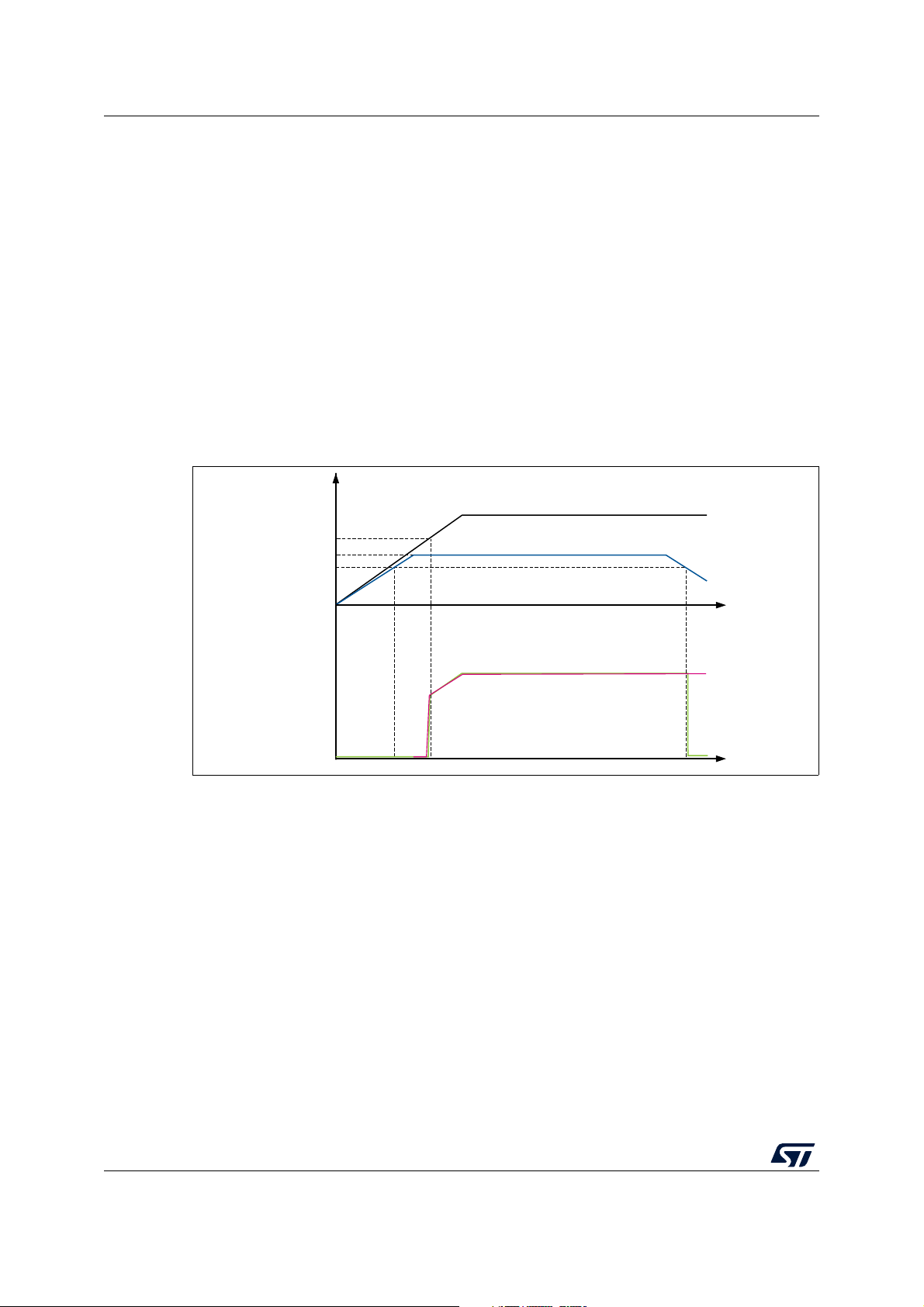
Functional overview STM32F479xx
ai18491g
V
DD
time
Min V
12
PDR = 1.7 or 1.8 V
V
CAP_1
,
V
CAP_2
V
12
NRST
time
PA0
The following conditions must be respected:
V
must always be higher than V
DD
CAP_1
and V
to avoid current injection between
CAP_2
power domains.
If the time for V
V
to reach 1.7 V, then PA0 must be kept low to cover both conditions: until V
DD
and V
CAP_2
reach V
Otherwise, if the time for V
than the time for V
and V
CAP_1
minimum value and until V
12
CAP_1
to reach 1.7 V, then PA0 can be asserted low externally (see
DD
CAP_2
to reach V
and V
CAP_2
minimum value is faster than the time for
12
reaches 1.7 V (see Figure 11).
DD
to reach V
minimum value is slower
12
CAP_1
Figure 12).
If V
CAP_1
and V
CAP_2
go below V
minimum value and VDD is higher than 1.7 V, then a
12
reset must be asserted on PA0 pin.
Note: The minimum value of V
(see Operating conditions).
Figure 11. Startup in regulator OFF: slow V
- power-down reset risen after V
1. This figure is valid whatever the internal reset mode (ON or OFF).
depends on the maximum frequency targeted in the application
12
slope
CAP_1
, V
CAP_2
DD
stabilization
34 /22 0 DS 1111 8 Rev 6
Page 35

STM32F479xx Functional overview
V
DD
time
Min V
12
V
CAP_1
, V
CAP_2
V
12
PA0
NRST
time
ai18492f
PDR = 1.7 or 1.8 V
(2)
Figure 12. Startup in regulator OFF mode: fast VDD slope
- power-down reset risen before V
1. This figure is valid whatever the internal reset mode (ON or OFF).
CAP_1
, V
CAP_2
stabilization
2.20.3 Regulator ON/OFF and internal reset ON/OFF availability
Table 4. Regulator ON/OFF and internal reset ON/OFF availability
Package Regulator ON Regulator OFF Internal reset ON Internal reset OFF
WLCSP168
UFBGA169
LQFP208
LQFP176
UFBGA176
TFBGA216
Yes No
Yes
BYPASS_REG set
to V
SS
Yes
BYPASS_REG set
to V
DD
Yes
PDR_ON set to V
PDR_ON set to V
DD
Yes
2.21 Real-time clock (RTC), backup SRAM and backup registers
The backup domain includes:
The real-time clock (RTC)
4 Kbytes of backup SRAM
20 backup registers
The real-time clock (RTC) is an independent BCD timer/counter. Dedicated registers contain
the second, minute, hour (in 12/24 hour), week day, date, month, year, in BCD (binarycoded decimal) format. Correction for 28, 29 (leap year), 30, and 31 day of the month are
performed automatically. The RTC provides a programmable alarm and programmable
periodic interrupts with wakeup from Stop and Standby modes. The sub-seconds value is
also available in binary format.
SS
It is clocked by a 32.768 kHz external crystal, resonator or oscillator, the internal low-power
RC oscillator or the high-speed external clock divided by 128. The internal low-speed RC
has a typical frequency of 32 kHz. The RTC can be calibrated using an external 512 Hz
output to compensate for any natural quartz deviation.
DS 1111 8 Rev 6 35/ 2 2 0
47
Page 36

Functional overview STM32F479xx
Two alarm registers are used to generate an alarm at a specific time and calendar fields can
be independently masked for alarm comparison. To generate a periodic interrupt, a 16-bit
programmable binary auto-reload downcounter with programmable resolution is available
and allows automatic wakeup and periodic alarms from every 120 µs to every 36 hours.
A 20-bit prescaler is used for the time base clock. It is by default configured to generate a
time base of 1 second from a clock at 32.768 kHz.
The 4-Kbyte backup SRAM is an EEPROM-like memory area. It can be used to store data
which need to be retained in VBAT and standby mode. This memory area is disabled by
default to minimize power consumption (see Section 2.22). It can be enabled by software.
The backup registers are 32-bit registers used to store 80 bytes of user application data
when V
power is not present. Backup registers are not reset by a system, a power reset,
DD
or when the device wakes up from the Standby mode (see Section 2.22).
Additional 32-bit registers contain the programmable alarm subseconds, seconds, minutes,
hours, day, and date.
Like backup SRAM, the RTC and backup registers are supplied through a switch that is
powered either from the V
supply when present or from the V
DD
BAT
pin.
2.22 Low-power modes
The devices support three low-power modes to achieve the best compromise between low
power consumption, short startup time and available wakeup sources:
Sleep mode
In Sleep mode, only the CPU is stopped. All peripherals continue to operate and can
wake up the CPU when an interrupt/event occurs.
Stop mode
The Stop mode achieves the lowest power consumption while retaining the contents of
SRAM and registers. All clocks in the 1.2 V domain are stopped, the PLL, the HSI RC
and the HSE crystal oscillators are disabled.
The voltage regulator can be put either in main regulator mode (MR) or in low-power
mode (LPR). Both modes can be configured as follows (see Tab le 5):
– Normal mode (default mode when MR or LPR is enabled)
– Under-drive mode.
The device can be woken up from the Stop mode by any of the EXTI line (the EXTI line
source can be one of the 16 external lines, the PVD output, the RTC alarm / wakeup /
tamper / time stamp events, the USB OTG FS/HS wakeup or the Ethernet wakeup).
Voltage regulator
configuration
Normal mode MR ON LPR ON
Table 5. Voltage regulator modes in stop mode
Main regulator (MR) Low-power regulator (LPR)
Under-drive mode MR in under-drive mode LPR in under-drive mode
Standby mode
The Standby mode is used to achieve the lowest power consumption. The internal
voltage regulator is switched off so that the entire 1.2 V domain is powered off. The
36 /22 0 DS 1111 8 Rev 6
Page 37

STM32F479xx Functional overview
PLL, the HSI RC and the HSE crystal oscillators are also switched off. After entering
Standby mode, the SRAM and register contents are lost except for registers in the
backup domain and the backup SRAM when selected.
The device exits the Standby mode when an external reset (NRST pin), an IWDG reset,
a rising edge on the WKUP pin, or an RTC alarm / wakeup / tamper /time stamp event
occurs.
The standby mode is not supported when the embedded voltage regulator is bypassed
and the 1.2 V domain is controlled by an external power.
2.23 V
The V
supercapacitor, or from V
operation
BAT
pin allows to power the device V
BAT
when no external battery neither an external supercapacitor are
DD
present.
V
operation is activated when VDD is not present.
BAT
The V
pin supplies the RTC, the backup registers and the backup SRAM.
BAT
Note: When the microcontroller is supplied from V
do not exit it from V
When PDR_ON pin is connected to V
more available and V
operation.
BAT
(Internal Reset OFF), the V
pin should be connected to VDD.
BAT
SS
2.24 Timers and watchdogs
The devices include two advanced-control timers, eight general-purpose timers, two basic
timers and two watchdog timers.
All timer counters can be frozen in debug mode.
Tab le 6 compares the features of the advanced-control, general-purpose and basic timers.
domain from an external battery, an external
BAT
, external interrupts and RTC alarm/events
BAT
functionality is no
BAT
DS 1111 8 Rev 6 37/ 2 2 0
47
Page 38

Functional overview STM32F479xx
Timer
type
Advanced
control
General
purpose
Basic
,
,
Counter
resolution
16-bit
32-bit
16-bit
16-bit Up
16-bit Up
16-bit Up
Timer
TIM1,
TIM8
TIM2,
TIM5
TIM3,
TIM4
TIM9 16-bit Up
TIM10
TIM11
TIM12 16-bit Up
TIM13
TIM14
TIM6,
TIM7
Counter
type
Up,
Down,
Up/down
Up,
Down,
Up/down
Up,
Down,
Up/down
Table 6. Timer feature comparison
Prescaler
factor
Any integer
between 1
and 65536
Any integer
between 1
and 65536
Any integer
between 1
and 65536
Any integer
between 1
and 65536
Any integer
between 1
and 65536
Any integer
between 1
and 65536
Any integer
between 1
and 65536
Any integer
between 1
and 65536
DMA
request
generation
Yes 4 Yes 90 180
Yes 4 No 45 90/180
Yes 4 No 45 90/180
No 2 No 90 180
No 1 No 90 180
No 2 No 45 90/180
No 1 No 45 90/180
Yes 0 No 45 90/180
Capture/
compare
channels
Complementary
output
Max
interface
clock
(MHz)
Max
timer
clock
(MHz)
(1)
1. The maximum timer clock is either 90 or 180 MHz depending on TIMPRE bit configuration in the
RCC_DCKCFGR register.
2.24.1 Advanced-control timers (TIM1, TIM8)
The advanced-control timers (TIM1, TIM8) can be seen as three-phase PWM generators
multiplexed on 6 channels. They have complementary PWM outputs with programmable
inserted dead times. They can also be considered as complete general-purpose timers.
Their 4 independent channels can be used for:
Input capture
Output compare
PWM generation (edge- or center-aligned modes)
One-pulse mode output
If configured as standard 16-bit timers, they have the same features as the general-purpose
TIMx timers. If configured as 16-bit PWM generators, they have full modulation capability (0100%).
The advanced-control timer can work together with the TIMx timers via the Timer Link
feature for synchronization or event chaining.
TIM1 and TIM8 support independent DMA request generation.
38 /22 0 DS 1111 8 Rev 6
Page 39

STM32F479xx Functional overview
2.24.2 General-purpose timers (TIMx)
There are ten synchronizable general-purpose timers embedded in the STM32F47x devices
(see Tab l e 6 for differences).
TIM2, TIM3, TIM4, TIM5
The STM32F47x include 4 full-featured general-purpose timers: TIM2, TIM5, TIM3,
and TIM4.The TIM2 and TIM5 timers are based on a 32-bit auto-reload up/down
counter and a 16-bit prescaler. The TIM3 and TIM4 timers are based on a 16-bit autoreload up/down counter and a 16-bit prescaler. They all feature 4 independent
channels for input capture/output compare, PWM or one-pulse mode output. This gives
up to 16 input capture/output compare/PWMs on the largest packages.
The TIM2, TIM3, TIM4, TIM5 general-purpose timers can work together, or with the
other general-purpose timers and the advanced-control timers TIM1 and TIM8 via the
Timer Link feature for synchronization or event chaining.
Any of these general-purpose timers can be used to generate PWM outputs.
TIM2, TIM3, TIM4, TIM5 all have independent DMA request generation. They are
capable of handling quadrature (incremental) encoder signals and the digital outputs
from 1 to 4 hall-effect sensors.
TIM9, TIM10, TIM11, TIM12, TIM13, and TIM14
These timers are based on a 16-bit auto-reload upcounter and a 16-bit prescaler.
TIM10, TIM11, TIM13, and TIM14 feature one independent channel, whereas TIM9
and TIM12 have two independent channels for input capture/output compare, PWM or
one-pulse mode output. They can be synchronized with the TIM2, TIM3, TIM4, TIM5
full-featured general-purpose timers. They can also be used as simple time bases.
2.24.3 Basic timers TIM6 and TIM7
These timers are mainly used for DAC trigger and waveform generation. They can also be
used as a generic 16-bit time base.
TIM6 and TIM7 support independent DMA request generation.
2.24.4 Independent watchdog
The independent watchdog is based on a 12-bit downcounter and 8-bit prescaler. It is
clocked from an independent 32 kHz internal RC and as it operates independently from the
main clock, it can operate in Stop and Standby modes. It can be used either as a watchdog
to reset the device when a problem occurs, or as a free-running timer for application timeout
management. It is hardware- or software-configurable through the option bytes.
2.24.5 Window watchdog
The window watchdog is based on a 7-bit downcounter that can be set as free-running. It
can be used as a watchdog to reset the device when a problem occurs. It is clocked from
the main clock. It has an early warning interrupt capability and the counter can be frozen in
debug mode.
DS 1111 8 Rev 6 39/ 2 2 0
47
Page 40

Functional overview STM32F479xx
2.24.6 SysTick timer
This timer is dedicated to real-time operating systems, but could also be used as a standard
downcounter. It features:
a 24-bit downcounter
autoreload capability
maskable system interrupt generation when the counter reaches 0
programmable clock source.
2.25 Inter-integrated circuit interface (I2C)
Up to three I²C bus interfaces can operate in multimaster and slave modes. They can
support the standard (up to 100 KHz), and fast (up to 400 KHz) modes. They support the
7/10-bit addressing mode and the 7-bit dual addressing mode (as slave). A hardware CRC
generation/verification is embedded.
The I²C bus interfaces can be served by DMA and support SMBus 2.0/PMBus.
The devices also include programmable analog and digital noise filters (see Tabl e 7).
Table 7. Comparison of I2C analog and digital filters
Filter Analog Digital
Pulse width of suppressed spikes 50 ns Programmable length, from one to fifteen I2C peripheral clocks
2.26 Universal synchronous/asynchronous receiver transmitters
(USART)
The devices embed four universal synchronous/asynchronous receiver transmitters
(USART1, USART2, USART3 and USART6) and four universal asynchronous receiver
transmitters (UART4, UART5, UART7, and UART8).
These six interfaces provide asynchronous communication, IrDA SIR ENDEC support,
multiprocessor communication mode, single-wire half-duplex communication mode and
have LIN Master/Slave capability. The USART1 and USART6 interfaces are able to
communicate at speeds of up to 11.25 Mbit/s. The other available interfaces communicate
at up to 5.62 bit/s.
USART1, USART2, USART3 and USART6 also provide hardware management of the CTS
and RTS signals, Smart Card mode (ISO 7816 compliant) and SPI-like communication
capability. All interfaces can be served by the DMA controller.
40 /22 0 DS 1111 8 Rev 6
Page 41

STM32F479xx Functional overview
Name
USART1 X X X X X X 5.62 11.25
USART2 X X X X X X 2.81 5.62
USART3 X X X X X X 2.81 5.62
UART4 X - X - X - 2.81 5.62
UART5 X - X - X - 2.81 5.62
USART6 X X X X X X 5.62 11.25
UART7 X - X - X - 2.81 5.62
UART8 X - X - X - 2.81 5.62
1. X = feature supported.
Standard
features
Modem
(RTS/CTS)
Table 8. USART feature comparison
LIN
SPI
master
irDA
Smartcard
(ISO 7816)
(1)
Max. baud rate in Mbit/s
Oversampling
by 16
Oversampling
by 8
APB
mapping
APB2
(max.
90 MHz)
APB1
(max.
45 MHz)
APB1
(max.
45 MHz)
APB1
(max.
45 MHz)
APB1
(max.
45 MHz)
APB2
(max.
90 MHz)
APB1
(max.
45 MHz)
APB1
(max.
45 MHz)
2.27 Serial peripheral interface (SPI)
The devices feature up to six SPIs in slave and master modes in full-duplex and simplex
communication modes. SPI1, SPI4, SPI5, and SPI6 can communicate at up to 45 Mbits/s,
SPI2 and SPI3 can communicate at up to 22.5 Mbit/s. The 3-bit prescaler gives 8 master
mode frequencies and the frame is configurable to 8 bits or 16 bits. The hardware CRC
generation/verification supports basic SD Card/MMC modes. All SPIs can be served by the
DMA controller.
The SPI interface can be configured to operate in TI mode for communications in master
mode and slave mode.
2.28 Inter-integrated sound (I2S)
Two standard I2S interfaces (multiplexed with SPI2 and SPI3) are available. They can be
operated in master or slave mode, in full duplex and simplex communication modes, and
can be configured to operate with a 16-/32-bit resolution as an input or output channel.
DS 1111 8 Rev 6 41/ 2 2 0
47
Page 42

Functional overview STM32F479xx
Audio sampling frequencies from 8 kHz up to 192 kHz are supported. When either or both of
2
the I
S interfaces is/are configured in master mode, the master clock can be output to the
external DAC/CODEC at 256 times the sampling frequency.
All I2Sx can be served by the DMA controller.
Note: For I2S2 full-duplex mode, I2S2_CK and I2S2_WS signals can be used only on GPIO Port
B and GPIO Port D.
2.29 Serial Audio interface (SAI1)
The serial audio interface (SAI1) is based on two independent audio sub-blocks which can
operate as transmitter or receiver with their FIFO. Many audio protocols are supported by
each block: I2S standards, LSB or MSB-justified, PCM/DSP, TDM, AC’97 and SPDIF
output, supporting audio sampling frequencies from 8 kHz up to 192 kHz. Both sub-blocks
can be configured in master or in slave mode.
In master mode, the master clock can be output to the external DAC/CODEC at 256 times of
the sampling frequency.
The two sub-blocks can be configured in synchronous mode when full-duplex mode is
required.
SAI1 can be served by the DMA controller.
2.30 Audio PLL (PLLI2S)
The devices feature an additional dedicated PLL for audio I2S and SAI applications. It allows
to achieve error-free I
performance, while using USB peripherals.
The PLLI2S configuration can be modified to manage an I
without disabling the main PLL (PLL) used for CPU, USB and Ethernet interfaces.
The audio PLL can be programmed with very low error to obtain sampling rates ranging
from 8 KHz to 192 KHz.
In addition to the audio PLL, a master clock input pin can be used to synchronize the
2
I
S/SAI flow with an external PLL (or Codec output).
2
S sampling clock accuracy without compromising on the CPU
2
S/SAI sample rate change
2.31 Audio and LCD PLL(PLLSAI)
An additional PLL dedicated to audio and LCD-TFT is used for SAI1 peripheral in case the
PLLI2S is programmed to achieve another audio sampling frequency (49.152 MHz or
11.2896 MHz) and the audio application requires both sampling frequencies simultaneously.
The PLLSAI is also used to generate the LCD-TFT clock.
2.32 Secure digital input/output interface (SDIO)
An SD/SDIO/MMC host interface is available, that supports MultiMediaCard System
Specification Version 4.2 in three different databus modes: 1-bit (default), 4-bit and 8-bit.
42 /22 0 DS 1111 8 Rev 6
Page 43

STM32F479xx Functional overview
The interface allows data transfer at up to 48 MHz, and is compliant with the SD Memory
Card Specification Version 2.0.
The SDIO Card Specification Version 2.0 is also supported with two different databus
modes: 1-bit (default) and 4-bit.
The current version supports only one SD/SDIO/MMC4.2 card at any one time and a stack
of MMC4.1 or previous.
In addition to SD/SDIO/MMC, this interface is fully compliant with the CE-ATA digital
protocol Rev1.1.
2.33 Ethernet MAC interface with dedicated DMA and IEEE 1588
support
The devices provide an IEEE-802.3-2002-compliant media access controller (MAC) for
ethernet LAN communications through an industry-standard medium-independent interface
(MII) or a reduced medium-independent interface (RMII). The microcontroller requires an
external physical interface device (PHY) to connect to the physical LAN bus (twisted-pair,
fiber, etc.). The PHY is connected to the device MII port using 17 signals for MII or 9 signals
for RMII, and can be clocked using the 25 MHz (MII) from the microcontroller.
The devices include the following features:
Supports 10 and 100 Mbit/s rates
Dedicated DMA controller allowing high-speed transfers between the dedicated SRAM
and the descriptors (see the STM32F4xx reference manual for details)
Tagged MAC frame support (VLAN support)
Half-duplex (CSMA/CD) and full-duplex operation
MAC control sublayer (control frames) support
32-bit CRC generation and removal
Several address filtering modes for physical and multicast address (multicast and
group addresses)
32-bit status code for each transmitted or received frame
Internal FIFOs to buffer transmit and receive frames. The transmit FIFO and the
receive FIFO are both 2 Kbytes.
Supports hardware PTP (precision time protocol) in accordance with IEEE 1588 2008
(PTP V2) with the time stamp comparator connected to the TIM2 input
Triggers interrupt when system time becomes greater than target time
2.34 Controller area network (bxCAN)
The two CANs are compliant with the 2.0A and B (active) specifications with a bitrate up to 1
Mbit/s. They can receive and transmit standard frames with 11-bit identifiers as well as
extended frames with 29-bit identifiers. Each CAN has three transmit mailboxes, two receive
FIFOS with 3 stages and 28 shared scalable filter banks (all of them can be used even if one
CAN is used). 256 bytes of SRAM are allocated for each CAN.
DS 1111 8 Rev 6 43/ 2 2 0
47
Page 44

Functional overview STM32F479xx
2.35 Universal serial bus on-the-go full-speed (OTG_FS)
The device embeds an USB OTG full-speed device/host/OTG peripheral with integrated
transceivers. The USB OTG FS peripheral is compliant with the USB 2.0 specification and
with the OTG 2.0 specification. It has software-configurable endpoint setting and supports
suspend/resume. The USB OTG controller requires a dedicated 48 MHz clock that is
generated by a PLL connected to the HSE oscillator.
The main features are:
Combined Rx and Tx FIFO size of 1.28 KB with dynamic FIFO sizing
Supports the session request protocol (SRP) and host negotiation protocol (HNP)
1 bidirectional control endpoint + 5 IN endpoints + 5 OUT endpoints
12 host channels with periodic OUT support
Software configurable to OTG1.3 and OTG2.0 modes of operation
USB 2.0 LPM (Link Power Management) support
Internal FS OTG PHY support
HNP/SNP/IP inside (no need for any external resistor)
For OTG/Host modes, a power switch is needed in case bus-powered devices are
connected
2.36 Universal serial bus on-the-go high-speed (OTG_HS)
The device embeds a USB OTG high-speed (up to 480 Mb/s) device/host/OTG peripheral.
The USB OTG HS supports both full-speed and high-speed operations. It integrates the
transceivers for full-speed operation (12 MB/s) and features a UTMI low-pin interface (ULPI)
for high-speed operation (480 MB/s). When using the USB OTG HS in HS mode, an
external PHY device connected to the ULPI is required.
The USB OTG HS peripheral is compliant with the USB 2.0 specification and with the OTG
2.0 specification. It has software-configurable endpoint setting and supports
suspend/resume. The USB OTG controller requires a dedicated 48 MHz clock that is
generated by a PLL connected to the HSE oscillator.
The main features are:
Combined Rx and Tx FIFO size of 4 KB with dynamic FIFO sizing
Supports the session request protocol (SRP) and host negotiation protocol (HNP)
8 bidirectional endpoints
16 host channels with periodic OUT support
Software configurable to OTG1.3 and OTG2.0 modes of operation
USB 2.0 LPM (Link Power Management) support
Internal FS OTG PHY support
External HS or HS OTG operation supporting ULPI in SDR mode. The OTG PHY is
connected to the microcontroller ULPI port through 12 signals. It can be clocked using
the 60 MHz output.
Internal USB DMA
HNP/SNP/IP inside (no need for any external resistor)
for OTG/Host modes, a power switch is needed in case bus-powered devices are
connected
44 /22 0 DS 1111 8 Rev 6
Page 45

STM32F479xx Functional overview
2.37 Digital camera interface (DCMI)
The devices embed a camera interface that can connect with camera modules and CMOS
sensors through an 8-bit to 14-bit parallel interface, to receive video data. The camera
interface can sustain a data transfer rate up to 54 Mbyte/s at 54 MHz. It features:
Programmable polarity for the input pixel clock and synchronization signals
Parallel data communication can be 8-, 10-, 12- or 14-bit
Supports 8-bit progressive video monochrome or raw bayer format, YCbCr 4:2:2
progressive video, RGB 565 progressive video or compressed data (like JPEG)
Supports continuous mode or snapshot (a single frame) mode
Capability to automatically crop the image black & white.
2.38 Cryptographic accelerator
The devices embed a cryptographic accelerator. This cryptographic accelerator provides a
set of hardware acceleration for the advanced cryptographic algorithms usually needed to
provide confidentiality, authentication, data integrity and non repudiation when exchanging
messages with a peer.
These algorithms consists of:
Encryption/Decryption
– DES/TDES (data encryption standard/triple data encryption standard): ECB
(electronic codebook) and CBC (cipher block chaining) chaining algorithms, 64,128- or 192-bit key
– AES (advanced encryption standard): ECB, CBC, GCM, CCM, and CTR (counter
mode) chaining algorithms, 128, 192 or 256-bit key
Universal hash
– SHA-1 and SHA-2 (secure hash algorithms)
–MD5
–HMAC
The cryptographic accelerator supports DMA request generation.
2.39 Random number generator (RNG)
All devices embed an RNG that delivers 32-bit random numbers generated by an integrated
analog circuit.
2.40 General-purpose input/outputs (GPIOs)
Each of the GPIO pins can be configured by software as output (push-pull or open-drain,
with or without pull-up or pull-down), as input (floating, with or without pull-up or pull-down)
or as peripheral alternate function. Most of the GPIO pins are shared with digital or analog
alternate functions. All GPIOs are high-current-capable and have speed selection to better
manage internal noise, power consumption and electromagnetic emission.
DS 1111 8 Rev 6 45/ 2 2 0
47
Page 46

Functional overview STM32F479xx
The I/O configuration can be locked if needed by following a specific sequence in order to
avoid spurious writing to the I/Os registers.
Fast I/O handling allowing maximum I/O toggling up to 90 MHz.
2.41 Analog-to-digital converters (ADCs)
Three 12-bit analog-to-digital converters are embedded and each ADC shares up to 16
external channels, performing conversions in the single-shot or scan mode. In scan mode,
automatic conversion is performed on a selected group of analog inputs.
Additional logic functions embedded in the ADC interface allow:
Simultaneous sample and hold
Interleaved sample and hold
The ADC can be served by the DMA controller. An analog watchdog feature allows very
precise monitoring of the converted voltage of one, some or all selected channels. An
interrupt is generated when the converted voltage is outside the programmed thresholds.
To synchronize A/D conversion and timers, the ADCs could be triggered by any of TIM1,
TIM2, TIM3, TIM4, TIM5, or TIM8 timer.
2.42 Temperature sensor
The temperature sensor has to generate a voltage that varies linearly with temperature. The
conversion range is between 1.7 V and 3.6 V. The temperature sensor is internally
connected to the same input channel as V
sensor output voltage into a digital value. When the temperature sensor and V
conversion are enabled at the same time, only V
As the offset of the temperature sensor varies from chip to chip due to process variation, the
internal temperature sensor is mainly suitable for applications that detect temperature
changes instead of absolute temperatures. If an accurate temperature reading is needed,
then an external temperature sensor part should be used.
, ADC1_IN18, which is used to convert the
BAT
2.43 Digital-to-analog converter (DAC)
The two 12-bit buffered DAC channels can be used to convert two digital signals into two
analog voltage signal outputs.
conversion is performed.
BAT
BAT
46 /22 0 DS 1111 8 Rev 6
Page 47

STM32F479xx Functional overview
This dual digital Interface supports the following features:
two DAC converters: one for each output channel
8-bit or 10-bit monotonic output
left or right data alignment in 12-bit mode
synchronized update capability
noise-wave generation
triangular-wave generation
dual DAC channel independent or simultaneous conversions
DMA capability for each channel
external triggers for conversion
input voltage reference V
Eight DAC trigger inputs are used in the device. The DAC channels are triggered through
the timer update outputs that are also connected to different DMA streams.
REF+
2.44 Serial wire JTAG debug port (SWJ-DP)
The Arm SWJ-DP interface is embedded, and is a combined JTAG and serial wire debug
port that enables either a serial wire debug or a JTAG probe to be connected to the target.
Debug is performed using 2 pins only instead of 5 required by the JTAG (JTAG pins could
be re-use as GPIO with alternate function): the JTAG TMS and TCK pins are shared with
SWDIO and SWCLK, respectively, and a specific sequence on the TMS pin is used to
switch between JTAG-DP and SW-DP.
2.45 Embedded Trace Macrocell™
The Arm Embedded Trace Macrocell provides a greater visibility of the instruction and data
flow inside the CPU core by streaming compressed data at a very high rate from the
STM32F47x through a small number of ETM pins to an external hardware trace port
analyzer (TPA) device. The TPA is connected to a host computer using USB, Ethernet, or
any other high-speed channel. Real-time instruction and data flow activity can be recorded
and then formatted for display on the host computer that runs the debugger software. TPA
hardware is commercially available from common development tool vendors.
The Embedded Trace Macrocell operates with third party debugger software tools.
DS 1111 8 Rev 6 47/ 2 2 0
47
Page 48

Pinouts and pin description STM32F479xx
MS40560V1
LQFP100
10
12
13
14
15
16
17
18
19
20
21
22
23
24
25
9
11
4
6
8
1
2
3
5
7
PH1
PC0
PC1
PC2
PC3
VSSA
VREF+
VDDA
PA0
PA1
PA2
PA3
VSS
VDD
PA4
PH0
NRST
PC13
PC15
VDD
PE2
VSS
VBAT
PC14
VSS
66
64
63
62
61
60
59
58
57
56
55
54
53
52
51
67
65
72
70
68
75
74
73
71
69
91
89888786858483828180797877
76
92
90
97
95
93
100
99
98
96
94
35
37383940414243444546474849
50
34
36
29
31
33
262728
30
32
PA5
PA6
PB1
PE8
PE12
PA7
PB0
PE9
PE14
PB11
PB2
PE7
PE15
VCAP1
PB12
PE10
PE11
VSS
PB13
PB15
PE13
PB10
VDD
PB14
PD8
PC6
DSIHOST_D1N
DSIHOST_D1P
VDD12DSI
DSIHOST_CKN
DSIHOST_CKP
VSSDSI
DSIHOST_D0N
DSIHOST_D0P
VCAPDSI
VDDDSI
PD15
PD14
PD10
PD9
PC7
VDDUSB
PA10
PA8
PC8
PA13
PA12
PA11
PA9
PC9
VDD
PB9
PB7
PB4
PD5
PB8
BOOT0
PB3
PD3
PD0
PB6
PB5
PD2
PC12
PA15
PD7
PD6
PC11
PA14
VDD
PD4
PD1
PC10
VSS
VCAP2
3 Pinouts and pin description
Figure 13. STM32F47x LQFP100 pinout
1. The above figure shows the package top view.
48 /22 0 DS 1111 8 Rev 6
Page 49

STM32F479xx Pinouts and pin description
MS40561V2
LQFP144
21
23
24
25
26
27
28
29
30
31
32
33
34
35
36
20
22
15
17
19
13
14
16
18
PC0
PC2
PC3
VDD
VSSA
VREF+
VDDA
PA0
PA1
PA2
PA3
VSS
VDD
PA4
PA5
NRST
PC1
VSS
PF10
PH1
PF4
PF5
VDD
PH0
88
86
85
84
83
82
81
80
79
78
77
76
75
74
73
89
87
94
92
90
97
96
95
93
91
135
133
132
131
130
129
128
127
126
125
124
123
122
121
136
134
141
139
137
144
143
142
140
138
47
49505152535455565758596061
72
46
48
41
43
45
383940
42
44
PA7
PC4
PB1
PF12
PF15
PC5
PB0
VDD
PG1
PE9
PB2
PF11
PE7
VSS
PE11
PF13
PF14
VDD
PE12
PE14
PG0
PE8
PE10
PE13
PD9
DSIHOST_D1P
DSIHOST_CKN
DSIHOST_CKP
VSSDSI
DSIHOST_D0N
DSIHOST_D0P
VCAPDSI
VDDDSI
PD15
PD14
VDD
VSS
PD12
PD11
PD10
DSIHOST_D1N
VDD12DSI
PG6
PG4
PG2
VDDUSB
PG8
PG7
PG5
PG3
PE2
VDD
PE0
BOOT0
PB4
PDR_ON
PE1
PB7
PG15
PG12
PB9
PB8
VDD
PG11
PD6
PB6
PB5
PG10
VDD
PD5
PB3
VSS
PG9
VSS
120 PD4
119 PD3
118 PD2
117 PD1
116 PD0
115 PC12
114 PC11
113 PC10
112 PA15
111 PA14
110 VDD
109 VSS
108 VCAP2
104
107
106
105
103
PA10
PA13
PA12
PA11
PA9
9998PC7
PC6
101
100
PC9
PC8
102 PA8
686970
71
PB13
PB14
PD8
PB15
646566
67
PB11
VCAP1
PB12
VDD
62
63
PE15
PB10
37
PA6
12
11
6
8
10
4
5
7
9
PF3
PF2
PC13
PC15
PF1
PE6
VBAT
PC14
PF0
3PE5
2PE4
1PE3
Figure 14. STM32F47x LQFP144 pinout
1. The above figure shows the package top view.
DS 1111 8 Rev 6 49/ 2 2 0
83
Page 50

Pinouts and pin description STM32F479xx
MSv35729V2
121110987654321
PI7 VDD PE0 PB7 PB3 VDD PG12 PD7 VSS PD1 PA15 PI2
PE5
A
B
C
D
E
F
G
H
J
K
L
M
N
P
PI6
VSS
PB8
PB5
VSS
PG11
VDD
PD4
PC11
PI3
PH13
VBAT
PE4
PI5
PE1
PB4
PG10
PD5
PD2
PC12
PI1
VDD
VSS
PC13
PE6
PI4
PDR_
ON
PG15
PG9
PD3
PC10
PA14
PH14
VCAP2
PA13
PC15
PC14
PE3
PB9
PG13
PD6
PD0
PI0
PH15
PA10
PA9
PA8
VSS
PI11
PI10
PE2
BOOT0
PA11
PA12
PC9
PC8
PC6
VSS
VDD
USB
PF2
VDD
PF0
PI9
PB6
PC7
PG8
PG2
PG3
PG6
PG4
PG5
PF5
PF3
PF1
NRST
PF15
VSS
PG7
PB12
PD13
DSI
HOST
_D1P
DSI
HOST
_D1N
VSS
DSI
VDD
VSS
PF4
PC0
PA7
PF13
PG0
PE14
PD11
DSI
HOST
_D0N
DSI
HOST
_CKN
DSI
HOST
_CKP
PH1
PH0
PF10
PA1
PH5
PF11
PE9
PB11
PB13
DSI
HOST
_D0P
VDD12
DSI
VCAP
DSI
PC1
VSSA
PA0
PA2
PA5
PF14
PE13
PH9
PD8
PD14
PD15
VDD
DSI
VDDA
PH2
PH4
PA4
PF12
PE8
PE12
PH8
PH10
PD10
PD12
VSS
PH3
VSS
PA3
PB1
VSS
PE7
PE11
VCAP1
PH11
PB15
PD9
PB10
VDD
PA6
PB0
PB2
VDD
PG1
PE10
PE15
VSS
VDD
PH12
PB14
Figure 15. STM32F47x WLCSP168 pinout
1. The above figure shows the package bottom view.
50 /22 0 DS 1111 8 Rev 6
Page 51
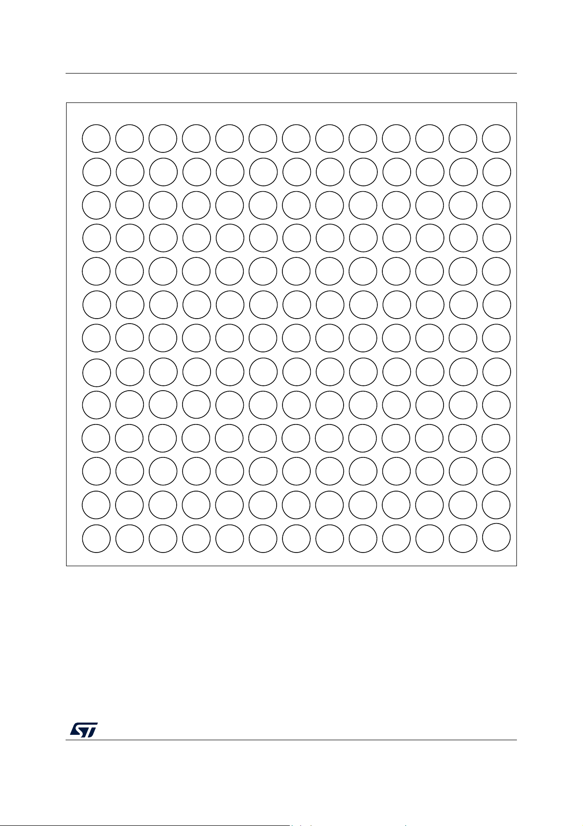
STM32F479xx Pinouts and pin description
MSv35730V2
PI6 PA11
A
PI5 BOOT0 PG12 PC12 PG13
PD7
PA14PE1 PE0 PA13 PA12
PI7 PI0
B
PE2 PB3 PD5 PC11PG11 PD2 PAI3PI4 PB7 PA15 PI2
PE3 PH14
C
PE4 PB6 PD1 PD0PD4 PD3 PC10
PDR_
ON
PB9 PI1 PH15
PE5 PG8
D
PE6 PB5 PD6 PH13PB4 PA8 VDDVDD PB8 VSS VCAP2
PC14 PG4
E
PI9 VBAT PG10 PA10PG9 PA9 PC8VSS PI10 PG7 PG5
PC15 PG2
F
PI11 VSS VDD PC6PG15
VSS
PC7PF0 VDD PG6 PG3
PH1
DSI
HOST_
D1N
G
PH0 PF2 VSS VSSPE8
VDD
PC9PF1 PC13
VDD
USB
DSI
HOST_
D1P
DSI_
HOST
CKN
H
NRST
PF14
PE10 PH9PE9
PH8
PH12
PF5
PF3
VSSDSI
DSI
HOST_
CKP
PF10
VSS
DSI
HOST_
D0N
VSSA PA0 VSS PH10VSS
PE13
VSSVDDA VDD
VDD12
DSI
DSI
HOST_
D0P
PA1
VDD
DSI
K
PA2 PB1 PE11 PH11VDD
PE14
VDDPA3 PA7 VSSDSI
VCAP
DSI
PH3 PD15
L
PH2 PB2 PE12 VDDVDD
PE15
PD8PH5 PF4 PD10 PD14
PC1 PB15
N
PA4 PF12 PE7 VCAP1PG0
PB11
PB12PA6 PB0 PB13 PB14
PC0 PD12
M
PH4 PF11 PG1 VSSPF15
PB10
PD9PA5 PF13 PD11 PD13
J
12345678910111213
Figure 16. STM32F47x UFBGA169 ballout
1. The above figure shows the package top view.
DS 1111 8 Rev 6 51/ 2 2 0
83
Page 52

Pinouts and pin description STM32F479xx
MS39400V2
123 910 11121314 15
APE3PE2
PE 1 P E 0 P B 8
PB5
PG14 PG13 PB4 PB3 PD7 PC12 PA15 PA14 PA13
BPE4PE5
PE6
PB9 PB7 PB6
PG15 PG 12 PG 11 PG 10 PD6 P D0 PC 11 PC10 P A12
C
VBAT
PI7 PI6 PI5
PDR
_ON
PG9 PD5 PD1 P I3
NC
D
PC13
PI8
PI9 PI4
BOOT0
VSS VSS VSS PD4 PD3 PD2
PI1
PA10
E
PC14
P F0 PI10
PI11
DSI
HOST_
D1P
PI0 PA 9
FPC15
VSS
VDD
PH2
V SS VCAP2 P C 9 PA 8
G
PH0 VSS VDD PH3
VSS VDD PC8 PC7
H
PH1
PF2
PF1
PH4
VSS
DSI
VDD_
USB
PG8 PC 6
J
NRST
PF3 PH5
PG7 PG 6
K
PF7
PF6
PF4
VDD
VSS
PG5 PG4 PG3
L
PF10
BYPASS
_REG
PG2
MVSSAPC0
PF8
PC1 P C 2 P C 3
PB2
PG1
VCAP
_1
PH6
PD14
NVREF-
PA0
PA4
PC4
PF13
P G 0 VDD V DD V DD P H 7 P D 12 P D 1 1 P D 10
P
P A2 PA6 P A5
PC5
PF12
PF15 PE8 PE 9 PE11 PB 12 PB 13 PD9 PD 8
R
PA3
PB1
PF11
PE7
PE12
P B 11 P B 14 P B 15
VSS
45678
PA1
VDD12
DSI
DSI
HOST_
D1N
VDD
DSI
VCAP
DSI
DSI
HOST_
CKP
DSI
HOST_
D0P
DSI
HOST_
D0N
DSI
HOST_
CKN
VDD
VDD
VDD
VDD
VREF+
VDDA
PA7
PB0
PF14
PE10
VSS VSS VSS VSS
VSSVSSVSS VSS VSS
VSSVSSVSS VSS VSS
VSSVSSVSS VSS VSS
VSSVSSVSS VSS VSS
VSS VSS
PF9
PF5
PD13
PD15
VDD PA11
PE13
PE14
PE15 PB10
Figure 17. STM32F47x UFBGA176 ballout
1. The above figure shows the package top view.
52 /22 0 DS 1111 8 Rev 6
Page 53

STM32F479xx Pinouts and pin description
MS33870V4
PDR_ON
VDD
PE1
PE0
PB9
PB8
BOOT0
PB7
PB6
PB5
PB4
PB3
PG15
VDD
VSS
PG14
PG13
PG12
PG11
PG10
PG9
PD7
PD6
VDD
VSS
PD5
PD4
PD3
PD2
PD1
PD0
PC12
PC11
PC10
PI7
PI6
PE2
PA12
PE3
PA11
PE4
PE5
PA9
PE6
PA8
VBAT
PC9
PI8
PC8
PC14
PC7
PC15
PC6
PF0
VDDUSB
PF1
VSS
PF2
PG8
PF3
PG7
PF4
PG6
PF5
PG5
PG4
PG3
PF6
PG2
PF7
VSSDSI
PF8
DSIHOST_D1N
PF9
DSIHOST_D1P
PF10
VDD12DSI
PH0
DSIHOST_CKN
PH1
DSIHOST_CKP
NRST
VSSDSI
PC0
DSIHOST_D0N
PC1
DSIHOST_D0P
PC2
VCAPDSI
PC3
VDDDSI
PD15
PD14
VREF+
VDD
VSS
PA0
PD13
PA1
PD12
PA2
PD11
PA3
BYPASS_REG
V
DD
PA4
PA5
PA6
PA7
PC4
PC5
PB0
PB1
PB2
PF11
PF12
VSS
PF13
PF14
PF15
PG0
PG1
PE7
PE8
PE9
PE10
PE11
PE12
PE13
PE14
PE15
PB10
PB11
VCAP_1
176
175
174
173
172
171
170
169
168
167
166
165
164
163
162
161
160
159
158
157
156
155
154
153
141
1
2
3
4
5
6
7
8
9
10
11
12
13
14
15
16
17
18
19
20
21
22
23
24
25
132
131
130
129
128
127
126
125
124
123
122
121
120
119
118
117
116
115
114
113
112
111
110
109
108
4546474849505152535455565758596061626364656667
68
80
LQFP176
152
151
150
149
148
147
146
145
144
143
142
6970717273747576777879
26
27
28
29
30
31
32
33
34
35
36
107
106
105
104
103
102
101
100
99
98
89
PA10
PI4
PA15
PA14
VDD
VSS
PI3
PI1
PI5
140
139
138
137
136
135
134
133
PH4
PH5
PH6
PH7
PB12
PB13
PB14
PB15
88
81828384858687
PI0
VDD
VSS
VCAP2
PA13
PD10
PD9
PD8
96
95
94
93
92
91
90
97
37
38
39
40
41
42
43
44
PC13
PI9
PI10
PI11
VSS
PH2
PH3
VDD
VSS
VDD
VDD
VSSA
VDDA
VDD
VSS
VDD
VDD
Figure 18. STM32F47x LQFP176 pinout
1. The above figure shows the package top view.
DS 1111 8 Rev 6 53/ 2 2 0
83
Page 54

Pinouts and pin description STM32F479xx
MSv33876V5
LQFP208
PI7
PI6
PI5
PI4
VDD
PDR_ON
VSS
PE1
PE0
PB9
PB8
BOOT0
PB7
PB6
PB5
PB4
PB3
PG15
PK7
PK6
PK5
PK4
PK3
VDD
VSS
PG14
PG13
PG12
PG11
PG10
PG9
PJ15
PJ14
PJ13
PJ12
PD7
PD6
VDD
VSS
PD5
PD4
PD3
PD2
PD1
PD0
PC12
PC11
PC10
PA15
PA14
VDD
PI3
208
207
206
205
204
203
202
201
200
199
198
197
196
195
194
193
192
191
190
189
188
187
186
185
184
183
182
181
180
179
178
177
176
175
174
173
172
171
170
169
168
167
166
165
164
163
162
161
160
159
158
157
PE2
1
156
PI2
PE3 2 155
PI1
PE4 3 154
PI0
PE5 4 153
PH15
PE6 5 152
PH14
VBAT 6 151
PH13
PI8 7 150
VDD
PC13 8 149
VSS
PC14 9 148
VCAP2
PC15 10 147
PA13
PI9 11 146
PA12
PI10 12 145
PA11
PI11 13 144
PA10
VSS 14 143
PA9
VDD 15 142
PA8
PF0 16 141
PC9
PF1 17 140
PC8
PF2 18 139
PC7
PI12 19 138
PC6
PI13 20 137
VDDUSB
PI14 21 136
VSS
PF3 22 135
PG8
PF4 23 134
PG7
PF5 24 133
PG6
VSS 25 132
PG5
VDD 26 131
PG4
PF6 27 130
PG3
PF7 28 129
PG2
PF8 29 128
VSSDSI
PF9 30 127
DSIHOST_D1N
PF10 31 126
DSIHOST_D1P
PH0 32 125
VDD12DSI
PH1 33 124
DSIHOST_CKN
NRST 34
123
DSIHOST_CKP
PC0 35 122
VSSDSI
PC1 36 121
DSIHOST_D0N
PC2 37 120
DSIHOST_D0P
PC3 38 119
VCAPDSI
VDD 39 11 8
VDDDSI
VSSA 40 11 7
PD15
VREF+ 41 116
PD14
VDDA 42 11 5
VDD
PA0 43 11 4
VSS
PA1 44 11 3
PD13
PA2 45 11 2
PD12
PH2 46 111
PD11
PH3 47 11 0
PD10
PH4 48 109
PD9
PH5 49 108
PD8
PA3 50 107
PB15
VSS 51 106
PB14
VDD
52
105 PB13
5354555657585960616263646566676869707172737475767778798081828384858687888990919293949596979899
100
101
102
103
104
PA4
PA5
PA6
PA7
PC4
PC5
VDD
VSS
PB0
PB1
PB2
PI15
PJ0
PJ1
PJ2
PJ3
PJ4
PF11
PF12
VSS
VDD
PF13
PF14
PF15
PG0
PG1
PE7
PE8
PE9
VSS
VDD
PE10
PE11
PE12
PE13
PE14
PE15
PB10
PB11
VCAP1
VSS
VDD
PJ5
PH6
PH7
PH8
PH9
PH10
PH11
PH12
VDD
PB12
Figure 19. STM32F47x LQFP208 pinout
54 /22 0 DS 1111 8 Rev 6
1. The above figure shows the package top view.
Page 55

STM32F479xx Pinouts and pin description
MSv33871V4
123 4 5678 910 1112131415
A
PG14
PE1
PE0
PB8
PB5
PB4
PB3
PD7
PC12 PA15
PA14 PA13
B
PE5 PE6 PG13 PB9
PB7
PB6
PG15
PG11 PJ13
PJ12 PD6
PD0
PC11 PC10
PA12
C
VBAT PI8
PI4
PK7 PK6 PK5
PG12
PG10 PJ14 PD5
PD1
PI3
PI2
PA11
D
PC13 PF0 PI5 PI7 PI10 PI6 PK4 PK3 PG9 PJ15 PD4 PD2 PH15 PI1 PA10
E
PC14 PF1 PI12 PI9 BOOT0 VDD
VDD
VDD VDD
VCAP2
PH13
PH14 PI0 PA9
F
PC15 VSS PI11
VDD
PC9
PA8
G
PH0
PF2
PI13
PI15
VDD
PC8 PC7
H
PH1 PI14
PH4
VSS PG8
PC6
J
NRST PF4 PH5
PH3
VSS
VDD
PG7
PG6
K
PF7
PF6
PF5
PH2
VDD
VSS
VSS VSS VSS VSS VDD
PD15
PB13
PD10
L
PF10
PC3
BYPASS-
REG
PB12
PD9 PD8
M
VSSA
PG1
PD12 PD13 PG3 PG2 PJ5 PH12
N
VREF- PA1
PA0
PA4
PC4
PF13
PG0 PJ3
PE8
PD11 PG5
PG4
PH7
PH9
PH11
VREF+
PA2
PA6 PA5 PC5 PF14 PJ2 PF11 PE9
PE11
PE14
PB10 PH6 PH8 PH10
PA3 PA7 PB1
PB0 PJ0
PJ1
PE7 PE10 PE12
PE15 PE13
PB11 PB14
PB15
PF3
P
R
VDDA
VDD
DSI
DSI
HOST_
CKP
VDDD
USB
VSS
DSI
VDD12
DSI
DSI
HOST_
CKN
DSI
HOST_
D0P
PDR
ON
VCAP
DSI
DSI
HOST_
D0N
DSI
HOST_
D1P
DSI
HOST_
D1N
PE4
PE3
PE2
VDD
VDD
VSS
VSS
VSS
VSS VSS VSS VSS VSS
VSS
VDD
PJ4PF15
VDD VDD VDD VCAP1 PD14
VDD
PF8
PF9
PC0
PC1 PC2 PB2 PF12
VDD
VSS
PD3
Figure 20. STM32F47x TFBGA216 ballout
1. The above figure shows the package top view.
DS 1111 8 Rev 6 55/ 2 2 0
83
Page 56

Pinouts and pin description STM32F479xx
Table 9. Legend/abbreviations used in the pinout table
Name Abbreviation Definition
Pin name
Unless otherwise specified in brackets below the pin name, the pin function during and after
reset is the same as the actual pin name
S Supply pin
Pin type
I Input only pin
I/O Input / output pin
FT 5 V tolerant I/O
TTa 3.3 V tolerant I/O directly connected to analog parts
I/O structure
B Dedicated BOOT0 pin
RST Bidirectional reset pin with weak pull-up resistor
Notes Unless otherwise specified by a note, all I/Os are set as floating inputs during and after reset
Alternate
functions
Additional
functions
Functions selected through GPIOx_AFR registers
Functions directly selected/enabled through peripheral registers
56 /22 0 DS 1111 8 Rev 6
Page 57
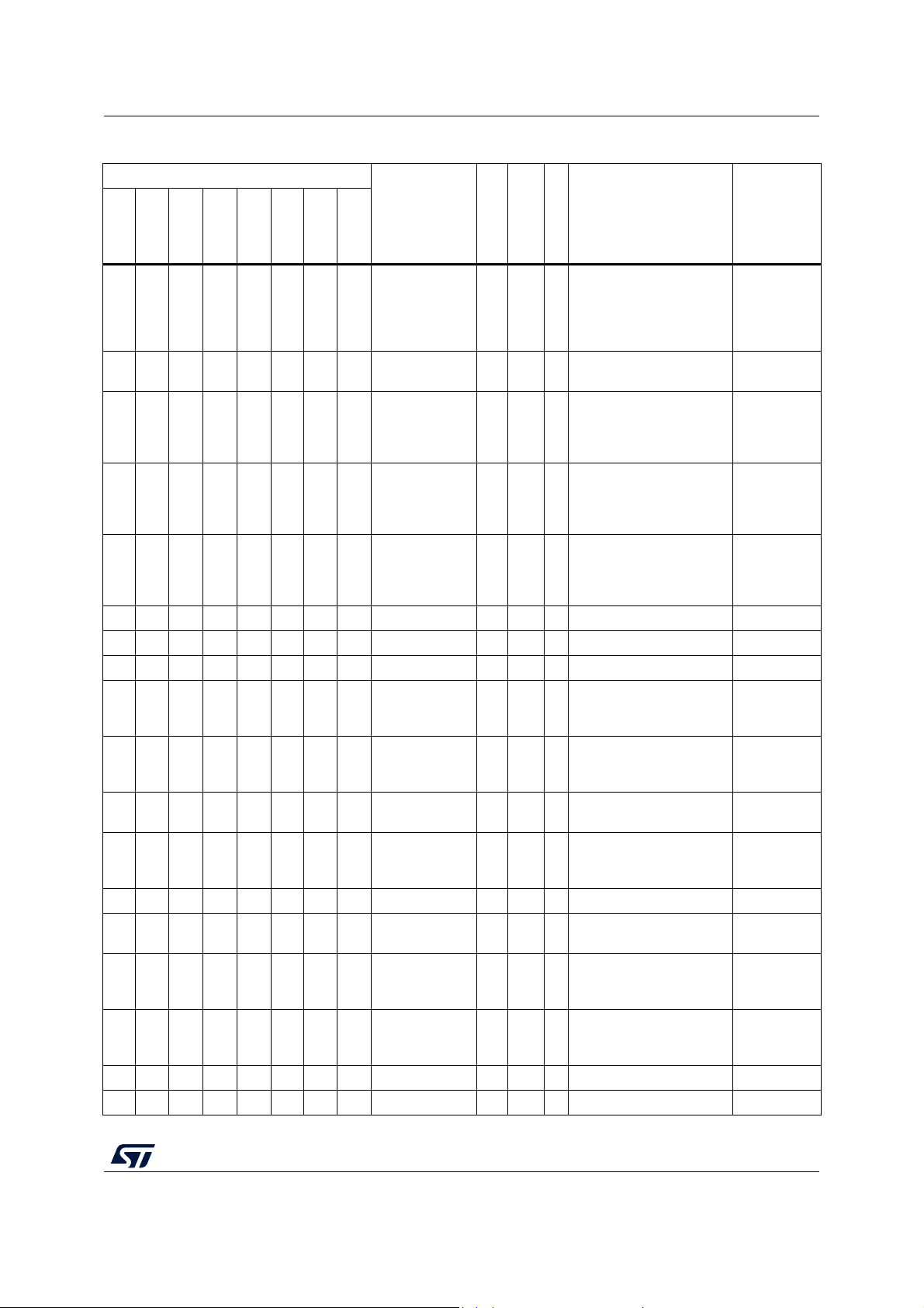
STM32F479xx Pinouts and pin description
Table 10. STM32F479xx pin and ball definitions
Pin number
LQFP100
LQFP144
UFBGA169
UFBGA176
WLCSP168
LQFP176
LQFP208
Pin name
(function after
reset)
TFBGA216
(1)
Pin types
Alternate functions
Notes
I/O structures
Additional
functions
TRACECLK, SPI4_SCK,
SAI1_MCLK_A,
1 144 B2 F9 A2 1 1 A3 PE2 I/O FT -
QUADSPI_BK1_IO2,
-
ETH_MII_TXD3, FMC_A23,
EVENTOUT
NC
1 C1 E10 A1 2 2 A2 PE3 I/O FT -
(2)
TRACED0, SAI1_SD_B,
FMC_A19, EVENTOUT
-
TRACED1, SPI4_NSS,
NC
2 C2 C11 B1 3 3 A1 PE4 I/O FT -
(2)
SAI1_FS_A, FMC_A20,
DCMI_D4, LCD_B0,
-
EVENTOUT
TRACED2, TIM9_CH1,
NC
3 D1 B12 B2 4 4 B1 PE5 I/O FT -
(2)
SPI4_MISO, SAI1_SCK_A,
FMC_A21, DCMI_D6,
-
LCD_G0, EVENTOUT
TRACED3, TIM9_CH2,
NC
4 D2 D11 B3 5 5 B2 PE6 I/O FT -
(2)
SPI4_MOSI, SAI1_SD_A,
FMC_A22, DCMI_D7,
-
LCD_G1, EVENTOUT
2------G6 VSS S-- - -
--- - ---F5 VDD S-- - -
3 5 E5 C12 C1 6 6 C1 VBAT S - - - -
- - - - D2 7 7 C2 PI8 I/O FT
(3)
(4)
EVENTOUT
RTC_TAMP1/
RTC_TAMP2/
RTC_TS
RTC_TAMP1/
RTC_TS/
4 6G4D12D18 8D1 PC13 I/OFT
(3)
(4)
EVENTOUT
RTC_OUT
5 7 E1 E11 E1 9 9 E1
68F1E12F11010F1
PC14-OSC32_IN
(PC14)
PC15-
OSC32_OUT
I/O FT
I/O FT
(3)
(4)
(3)
(4)
EVENTOUT OSC32_IN
EVENTOUT OSC32_OUT
(PC15)
--- - ---G5 VDD S-- - -
- - E2 G9 D3 11 11 E4 PI9 I/O FT
CAN1_RX, FMC_D30,
LCD_VSYNC, EVENTOUT
-
ETH_MII_RX_ER,
- - E4 F10 E3 12 12 D5 PI10 I/O FT
FMC_D31, LCD_HSYNC,
-
EVENTOUT
LCD_G6,
- - F2 F11 E4 13 13 F3 PI11 I/O FT
OTG_HS_ULPI_DIR,
-
EVENTOUT
- - F5 F12 F2 14 14 F2 VSS S - - - -
--F4G11F31515F4 VDD S-- - -
DS 1111 8 Rev 6 57/ 2 2 0
83
Page 58

Pinouts and pin description STM32F479xx
Table 10. STM32F479xx pin and ball definitions (continued)
Pin number
Pin name
(function after
LQFP100
LQFP144
UFBGA169
WLCSP168
UFBGA176
LQFP176
LQFP208
TFBGA216
reset)
(1)
Pin types
- 9 F3 G10 E2 16 16 D2 PF0 I/O FT
- 10 G3 H10 H3 17 17 E2 PF1 I/O FT
- 11 G5 G12 H2 18 18 G2 PF2 I/O FT
I/O structures
Alternate functions
Notes
I2C2_SDA, FMC_A0,
EVENTOUT
I2C2_SCL, FMC_A1,
EVENTOUT
I2C2_SMBA, FMC_A2,
EVENTOUT
- - - - - - 19 E3 PI12 I/O FT LCD_HSYNC, EVENTOUT -
- - - - - - 20 G3 PI13 I/O FT LCD_VSYNC, EVENTOUT -
- - - - - - 21 H3 PI14 I/O FT LCD_CLK, EVENTOUT -
- 12 H4 H11 J2 19 22 H2 PF3 I/O FT
- 13 L4 J10 J3 20 23 J2 PF4 I/O FT
- 14 H3 H12 K3 21 24 K3 PF5 I/O FT
(5)
FMC_A3, EVENTOUT ADC3_IN9
(5)
FMC_A4, EVENTOUT ADC3_IN14
(5)
FMC_A5, EVENTOUT ADC3_IN15
7 15 G7 J11 G2 22 25 H6 VSS S - - - -
8 16 G8 J12 G3 23 26 H5 VDD S - - - -
TIM10_CH1, SPI5_NSS,
SAI1_SD_B, UART7_Rx,
- - - - K2 24 27 K2 PF6 I/O FT
(5)
QUADSPI_BK1_IO3,
EVENTOUT
TIM11_CH1, SPI5_SCK,
SAI1_MCLK_B, UART7_Tx,
- - - - K1 25 28 K1 PF7 I/O FT
(5)
QUADSPI_BK1_IO2,
EVENTOUT
SPI5_MISO, SAI1_SCK_B,
- - - - L3 26 29 L3 PF8 I/O FT
(5)
TIM13_CH1,
QUADSPI_BK1_IO0,
EVENTOUT
SPI5_MOSI, SAI1_FS_B,
- - - - L2 27 30 L2 PF9 I/O FT
(5)
TIM14_CH1,
QUADSPI_BK1_IO1,
EVENTOUT
QUADSPI_CLK,
DCMI_D11, LCD_DE,
- 17 H1 K10 L1 28 31 L1 PF10 I/O FT
(5)
EVENTOUT
9 18 G2 K11 G1 29 32 G1
10 19 G1 K12 H1 30 33 H1
PH0-OSC_IN
(PH0)
PH1-OSC_OUT
(PH1)
I/O FT - EVENTOUT OSC_IN
I/O FT - EVENTOUT OSC_OUT
11 20 H2 H9 J1 31 34 J1 NRST I/O RST -
OTG_HS_ULPI_STP,
12 21 M1 J9 M2 32 35 M2 PC0 I/O FT
(5)
FMC_SDNWE, LCD_R5,
EVENTOUT
Additional
functions
-
-
-
ADC3_IN4
ADC3_IN5
ADC3_IN6
ADC3_IN7
ADC3_IN8
ADC123_
IN10
58 /22 0 DS 1111 8 Rev 6
Page 59

STM32F479xx Pinouts and pin description
Table 10. STM32F479xx pin and ball definitions (continued)
Pin number
Pin name
(function after
LQFP100
LQFP144
UFBGA169
WLCSP168
UFBGA176
LQFP176
LQFP208
TFBGA216
reset)
(1)
Pin types
I/O structures
Alternate functions
Notes
TRACED0,
SPI2_MOSI/I2S2_SD,
13 22 N1 L12 M3 33 36 M3 PC1 I/O FT
(5)
SAI1_SD_A, ETH_MDC,
EVENTOUT
SPI2_MISO, I2S2ext_SD,
OTG_HS_ULPI_DIR,
14 23 - - M4 34 37 M4 PC2 I/O FT
(5)
ETH_MII_TXD2,
FMC_SDNE0, EVENTOUT
SPI2_MOSI/I2S2_SD,
OTG_HS_ULPI_NXT,
15 24 - - M5 35 38 L4 PC3 I/O FT
(5)
ETH_MII_TX_CLK,
FMC_SDCKE0,
EVENTOUT
- 25 - - - 36 39 J5 VDD S - - - -
--- - ---J6 VSS S-- - -
16 26 J2 L11 M1 37 40 M1 VSSA S - - - -
--- -N1--N1 VREF- S-- - -
17 27 - - P1 38 41 P1 VREF+ S - - - -
18 28 J3 M12 R1 39 42 R1 VDDA S - - - -
TIM2_CH1/TIM2_ETR,
TIM5_CH1, TIM8_ETR,
19 29 J5 L10 N3 40 43 N3 PA0-WKUP(PA0) I/O FT
(6)
USART2_CTS, UART4_TX,
ETH_MII_CRS,
EVENTOUT
TIM2_CH2, TIM5_CH2,
USART2_RTS, UART4_RX,
QUADSPI_BK1_IO3,
20 30 K1 K9 N2 41 44 N2 PA1 I/O FT
(5)
ETH_MII_RX_CLK/ETH_R
MII_REF_CLK, LCD_R2,
EVENTOUT
TIM2_CH3, TIM5_CH3,
TIM9_CH1, USART2_TX,
21 31 K2 L9 P2 42 45 P2 PA2 I/O FT
(5)
ETH_MDIO, LCD_R1,
EVENTOUT
QUADSPI_BK2_IO0,
- - L2 M11 F4 43 46 K4 PH2 I/O FT -
ETH_MII_CRS,
FMC_SDCKE0, LCD_R0,
EVENTOUT
QUADSPI_BK2_IO1,
- - L1 N12 G4 44 47 J4 PH3 I/O FT -
ETH_MII_COL,
FMC_SDNE0, LCD_R1,
EVENTOUT
I2C2_SCL, LCD_G5,
- - M2 M10 H4 45 48 H4 PH4 I/O FT -
OTG_HS_ULPI_NXT,
LCD_G4, EVENTOUT
Additional
functions
ADC123_
IN11
ADC123_
IN12
ADC123_
IN13
ADC123_IN0,
WKUP
ADC123_IN1
ADC123_IN2
-
-
-
DS 1111 8 Rev 6 59/ 2 2 0
83
Page 60

Pinouts and pin description STM32F479xx
Table 10. STM32F479xx pin and ball definitions (continued)
Pin number
Pin name
(function after
LQFP100
LQFP144
UFBGA169
WLCSP168
UFBGA176
LQFP176
LQFP208
TFBGA216
reset)
(1)
Pin types
I/O structures
- - L3 K8 J4 46 49 J3 PH5 I/O FT -
Alternate functions
Notes
I2C2_SDA, SPI5_NSS,
FMC_SDNWE, EVENTOUT
TIM2_CH4, TIM5_CH4,
TIM9_CH2, USART2_RX,
22 32 K3 N10 R2 47 50 R2 PA3 I/O FT
(5)
LCD_B2,
OTG_HS_ULPI_D0,
ETH_MII_COL, LCD_B5,
EVENTOUT
23 33 J1 N11 - - 51 K6 VSS S - - - -
- - - - L4 48 - L5 BYPASS_REG I FT - - -
24 34 J4 P12 K4 49 52 K5 VDD S - - - -
SPI1_NSS,
SPI3_NSS/I2S3_WS,
25 35 N2 M9 N4 50 53 N4 PA4 I/O TTa -
USART2_CK,
OTG_HS_SOF,
DCMI_HSYNC,
LCD_VSYNC, EVENTOUT
TIM2_CH1/TIM2_ETR,
26 36 M3 L8 P4 51 54 P4 PA5 I/O TTa -
TIM8_CH1N, SPI1_SCK,
OTG_HS_ULPI_CK,
LCD_R4, EVENTOUT
TIM1_BKIN, TIM3_CH1,
TIM8_BKIN, SPI1_MISO,
27 37 N3 P11 P3 52 55 P3 PA6 I/O FT
(5)
TIM13_CH1,
DCMI_PIXCLK, LCD_G2,
EVENTOUT
TIM1_CH1N, TIM3_CH2,
TIM8_CH1N, SPI1_MOSI,
28 38 K4 J8 R3 53 56 R3 PA7 I/O FT
(5)
TIM14_CH1,
QUADSPI_CLK,
ETH_MII_RX_DV/ETH_RMI
I_CRS_DV, FMC_SDNWE,
EVENTOUT
NC
39 - - N5 54 57 N5 PC4 I/O FT
(2)
ETH_MII_RXD0/ETH_RMII
(5)
_RXD0, FMC_SDNE0,
EVENTOUT
NC
40 - - P5 55 58 P5 PC5 I/O FT
(2)
ETH_MII_RXD1/ETH_RMII
(5)
_RXD1, FMC_SDCKE0,
EVENTOUT
------59L7 VDD S-- - -
------60L6 VSS S-- - -
TIM1_CH2N, TIM3_CH3,
TIM8_CH2N, LCD_R3,
(5)
29 41 N4 P10 R5 56 61 R5 PB0 I/O FT
OTG_HS_ULPI_D1,
ETH_MII_RXD2, LCD_G1,
EVENTOUT
Additional
functions
-
ADC123_IN3
ADC12_IN4,
DAC_OUT1
ADC12_IN5,
DAC_OUT2
ADC12_IN6
ADC12_IN7
ADC12_IN14
ADC12_IN15
ADC12_IN8
60 /22 0 DS 1111 8 Rev 6
Page 61

STM32F479xx Pinouts and pin description
Table 10. STM32F479xx pin and ball definitions (continued)
Pin number
Pin name
(function after
LQFP100
LQFP144
UFBGA169
WLCSP168
30 42 K5 N9 R4 57 62 R4 PB1 I/O FT
31 43 L5 P9 M6 58 63 M5
- - - - - - 64 G4 PI15 I/O FT -
------65R6 PJ0 I/OFT-
- - - - - - 66 R7 PJ1 I/O FT - LCD_R2, EVENTOUT -
------67P7 PJ2 I/OFT-
- - - - - - 68 N8 PJ3 I/O FT - LCD_R4, EVENTOUT -
- - - - - - 69 M9 PJ4 I/O FT - LCD_R5, EVENTOUT -
- 44M5K7R65970P8 PF11 I/OFT -
- 45 N5 M8 P6 60 71 M6 PF12 I/O FT - FMC_A6, EVENTOUT -
- - J6 N8 M8 61 72 K7 VSS S - - - -
- 46K6P8N86273L8 VDD S - - - -
- 47M4J7N66374N6 PF13 I/OFT - FMC_A7, EVENTOUT -
- 48H5L7R76475P6 PF14 I/OFT - FMC_A8, EVENTOUT -
- 49M6H8P7 65 76M8 PF15 I/OFT - FMC_A9, EVENTOUT -
- 50N6J6N76677N7 PG0 I/OFT - FMC_A10, EVENTOUT -
- 51M7P7M767 78M7 PG1 I/OFT - FMC_A11, EVENTOUT -
32 52 N7 N7 R8 68 79 R8 PE7 I/O FT -
33 53 G6 M7 P8 69 80 N9 PE8 I/O FT -
34 54 H6 K6 P9 70 81 P9 PE9 I/O FT -
- 55 J7 - M9 71 82 K8 VSS S - - - -
- 56 L6 - N9 72 83 L9 VDD S - - - -
35 57 H7 P6 R9 73 84 R9 PE10 I/O FT -
UFBGA176
LQFP176
LQFP208
TFBGA216
BOOT1(PB2)
reset)
PB2-
(1)
Pin types
I/O structures
I/O FT - EVENTOUT -
Alternate functions
Notes
TIM1_CH3N, TIM3_CH4,
TIM8_CH3N, LCD_R6,
(5)
OTG_HS_ULPI_D2,
ETH_MII_RXD3, LCD_G0,
EVENTOUT
LCD_G2, LCD_R0,
EVENTOUT
LCD_R7, LCD_R1,
EVENTOUT
DSIHOST_TE, LCD_R3,
EVENTOUT
SPI5_MOSI,
FMC_SDNRAS,
DCMI_D12, EVENTOUT
TIM1_ETR, UART7_Rx,
QUADSPI_BK2_IO0,
FMC_D4, EVENTOUT
TIM1_CH1N, UART7_Tx,
QUADSPI_BK2_IO1,
FMC_D5, EVENTOUT
TIM1_CH1,
QUADSPI_BK2_IO2,
FMC_D6, EVENTOUT
TIM1_CH2N,
QUADSPI_BK2_IO3,
FMC_D7, EVENTOUT
Additional
functions
ADC12_IN9
-
-
-
-
-
-
-
-
DS 1111 8 Rev 6 61/ 2 2 0
83
Page 62

Pinouts and pin description STM32F479xx
Table 10. STM32F479xx pin and ball definitions (continued)
Pin number
Pin name
(function after
LQFP100
LQFP144
UFBGA169
WLCSP168
36 58 K7 N6 P10 74 85 P10 PE11 I/O FT -
37 59 L7 M6 R10 75 86 R10 PE12 I/O FT -
38 60 J8 L6 N11 76 87 R12 PE13 I/O FT -
39 61 K8 J5 P11 77 88 P11 PE14 I/O FT -
40 62 L8 P5 R11 78 89 R11 PE15 I/O FT -
41 63 M8 N5 R12 79 90 P12 PB10 I/O FT -
42 64 N8 K5 R13 80 91 R13 PB11 I/O FT -
43 65 N9 N4 M10 81 92 L11 VCAP1 S - - - -
44 - M9 P4 - - 93 K9 VSS S - - - -
45 66 L9 P3 N10 82 94 L10 VDD S - - - -
- - - - - - 95 M14 PJ5 I/O FT - LCD_R6, EVENTOUT -
- - - - M11 83 96 P13 PH6 I/O FT -
- - - - N12 84 97 N13 PH7 I/O FT -
- - H8 M5 - - 98 P14 PH8 I/O FT -
- - H9 L5 - - 99 N14 PH9 I/O FT -
UFBGA176
LQFP176
LQFP208
TFBGA216
reset)
(1)
Pin types
I/O structures
Alternate functions
Notes
TIM1_CH2, SPI4_NSS,
FMC_D8, LCD_G3,
EVENTOUT
TIM1_CH3N, SPI4_SCK,
FMC_D9, LCD_B4,
EVENTOUT
TIM1_CH3, SPI4_MISO,
FMC_D10, LCD_DE,
EVENTOUT
TIM1_CH4, SPI4_MOSI,
FMC_D11, LCD_CLK,
EVENTOUT
TIM1_BKIN, FMC_D12,
LCD_R7, EVENTOUT
TIM2_CH3, I2C2_SCL,
SPI2_SCK/I2S2_CK,
USART3_TX,
QUADSPI_BK1_NCS,
OTG_HS_ULPI_D3,
ETH_MII_RX_ER, LCD_G4,
EVENTOUT
TIM2_CH4, I2C2_SDA,
USART3_RX,
OTG_HS_ULPI_D4,
ETH_MII_TX_EN/ETH_RMI
I_TX_EN, DSIHOST_TE,
LCD_G5, EVENTOUT
I2C2_SMBA, SPI5_SCK,
TIM12_CH1,
ETH_MII_RXD2,
FMC_SDNE1, DCMI_D8,
EVENTOUT
I2C3_SCL, SPI5_MISO,
ETH_MII_RXD3,
FMC_SDCKE1, DCMI_D9,
EVENTOUT
I2C3_SDA, FMC_D16,
DCMI_HSYNC, LCD_R2,
EVENTOUT
I2C3_SMBA, TIM12_CH2,
FMC_D17, DCMI_D0,
LCD_R3, EVENTOUT
Additional
functions
-
-
-
-
-
-
-
-
-
-
-
62 /22 0 DS 1111 8 Rev 6
Page 63

STM32F479xx Pinouts and pin description
Table 10. STM32F479xx pin and ball definitions (continued)
Pin number
Pin name
(function after
LQFP100
LQFP144
UFBGA169
WLCSP168
- - J9 M4 - - 100 P15 PH10 I/O FT -
- - K9 N3 - - 101 N15 PH11 I/O FT -
- - H10 P2 - - 102 M15 PH12 I/O FT -
---H7---K10 VSS S-- - -
-66----103K11 VDD S-- - -
46 67 N10 H5 P12 85 104 L13 PB12 I/O FT -
47 68 N11 K4 P13 86 105 K14 PB13 I/O FT -
48 69 N12 P1 R14 87 106 R14 PB14 I/O FT -
49 70 N13 N2 R15 88 107 R15 PB15 I/O FT -
50 71 L10 L4 P15 89 108 L15 PD8 I/O FT -
51 72 M10 N1 P14 90 109 L14 PD9 I/O FT -
52 73 L11 M3 N15 91 110 K15 PD10 I/O FT -
- 74 M11 J4 N14 92 111 N10 PD11 I/O FT -
UFBGA176
LQFP176
LQFP208
TFBGA216
reset)
(1)
Pin types
I/O structures
Alternate functions
Notes
TIM5_CH1, FMC_D18,
DCMI_D1, LCD_R4,
EVENTOUT
TIM5_CH2, FMC_D19,
DCMI_D2, LCD_R5,
EVENTOUT
TIM5_CH3, FMC_D20,
DCMI_D3, LCD_R6,
EVENTOUT
TIM1_BKIN, I2C2_SMBA,
SPI2_NSS/I2S2_WS,
USART3_CK, CAN2_RX,
OTG_HS_ULPI_D5,
ETH_MII_TXD0/ETH_RMII
_TXD0, OTG_HS_ID,
EVENTOUT
TIM1_CH1N,
SPI2_SCK/I2S2_CK,
USART3_CTS, CAN2_TX,
OTG_HS_ULPI_D6,
ETH_MII_TXD1/ETH_RMII
_TXD1, EVENTOUT
TIM1_CH2N, TIM8_CH2N,
SPI2_MISO, I2S2ext_SD,
USART3_RTS,
TIM12_CH1, OTG_HS_DM,
EVENTOUT
RTC_REFIN, TIM1_CH3N,
TIM8_CH3N,
SPI2_MOSI/I2S2_SD,
TIM12_CH2, OTG_HS_DP,
EVENTOUT
USART3_TX, FMC_D13,
EVENTOUT
USART3_RX, FMC_D14,
EVENTOUT
USART3_CK, FMC_D15,
LCD_B3, EVENTOUT
USART3_CTS,
QUADSPI_BK1_IO0,
FMC_A16/FMC_CLE,
EVENTOUT
Additional
functions
-
-
-
-
OTG_HS_
VBUS
-
-
-
-
-
-
DS 1111 8 Rev 6 63/ 2 2 0
83
Page 64

Pinouts and pin description STM32F479xx
Table 10. STM32F479xx pin and ball definitions (continued)
Pin number
Pin name
(function after
LQFP100
LQFP144
UFBGA169
WLCSP168
- 75 M13 M2 N13 93 112 M10 PD12 I/O FT -
- - M12 H4 M15 94 113 M11 PD13 I/O FT -
- 76 J10 M1 - 95 114 J10 VSS S - - - -
- 77 K10 - J13 96 115 J11 VDD S - - - -
53 78 L12 L3 M14 97 116 L12 PD14 I/O FT -
54 79 L13 L2 L14 98 117 K13 PD15 I/O FT -
55 80 K13 L1 J12 99 118 H11 VDDDSI S - - - -
--- - ---H10 VSS S-- - -
56 81 K12 K1 K12 100 119 K12 VCAPDSI S - - - -
- - - K2 D13 - - G13 VDD12DSI S - - - -
57 82 J12 K3 M12 101 120 J12 DSIHOST_D0P I/O - - - -
58 83 J13 J3 M13 102 121 J13 DSIHOST_D0N I/O - - - -
59 84 K11 H1 H12 103 122 G12 VSSDSI S - - - -
60 85 H12 J1 L12 104 123 H12 DSIHOST_CKP I/O - - - -
61 86 H13 J2 L13 105 124 H13 DSIHOST_CKN I/O - - - -
62 87 J11 - D13 106 125 - VDD12DSI S - - - -
63 88 G12 H3 E12 107 126 F12 DSIHOST_D1P I/O - - - -
64 89 G13 H2 E13 108 127 F13 DSIHOST_D1N I/O - - - -
- - H11 - H12 109 128 - VSSDSI S - - - -
- 90 F13 G5 L15 110 129 M13 PG2 I/O FT - FMC_A12, EVENTOUT -
- 91 F12 G4 K15 111 130 M12 PG3 I/O FT - FMC_A13, EVENTOUT -
- 92 E13 G2 K14 112 131 N12 PG4 I/O FT -
- 93 E12 G1 K13 113 132 N11 PG5 I/O FT -
- 94 F11 G3 J15 114 133 J15 PG6 I/O FT -
- 95 E11 H6 J14 115 134 J14 PG7 I/O FT -
UFBGA176
LQFP176
LQFP208
TFBGA216
reset)
(1)
Pin types
I/O structures
Alternate functions
Notes
TIM4_CH1, USART3_RTS,
QUADSPI_BK1_IO1,
FMC_A17/FMC_ALE,
EVENTOUT
TIM4_CH2,
QUADSPI_BK1_IO3,
FMC_A18, EVENTOUT
TIM4_CH3, FMC_D0,
EVENTOUT
TIM4_CH4, FMC_D1,
EVENTOUT
FMC_A14/FMC_BA0,
EVENTOUT
FMC_A15/FMC_BA1,
EVENTOUT
DCMI_D12, LCD_R7,
EVENTOUT
SAI1_MCLK_A,
USART6_CK, FMC_INT,
DCMI_D13, LCD_CLK,
EVENTOUT
Additional
functions
-
-
-
-
-
-
-
-
64 /22 0 DS 1111 8 Rev 6
Page 65
STM32F479xx Pinouts and pin description
Table 10. STM32F479xx pin and ball definitions (continued)
Pin number
Pin name
(function after
LQFP100
LQFP144
UFBGA169
WLCSP168
- 96 D13 G6 H14 116 135 H14 PG8 I/O FT -
- - G9 F2 G12 117 136 G10 VSS S - - - -
65 97 G11 F1 H13 118 137 G11 VDDUSB S - - - -
66 98 F9 F3 H15 119 138 H15 PC6 I/O FT -
67 99 F10 G7 G15 120 139 G15 PC7 I/O FT -
68 100 E10 F4 G14 121 140 G14 PC8 I/O FT -
69 101 G10 F5 F14 122 141 F14 PC9 I/O FT -
70 102 D8 E1 F15 123 142 F15 PA8 I/O FT -
71 103 E8 E2 E15 124 143 E15 PA9 I/O FT -
72 104 E9 E3 D15 125 144 D15 PA10 I/O FT -
73 105 A13 F7 C15 126 145 C15 PA11 I/O FT -
74 106 A12 F6 B15 127 146 B15 PA12 I/O FT -
75 107 A11 D1 A15 128 147 A15
76 108 D12 D2 F13 129 148 E11 VCAP2 S - - - -
- 109 D11 C1 F12 130 149 F10 VSS S - - - -
UFBGA176
LQFP176
LQFP208
TFBGA216
PA13(JTMS-
reset)
SWDIO)
(1)
Pin types
I/O structures
I/O FT - JTMS-SWDIO, EVENTOUT -
Alternate functions
Notes
SPI6_NSS, USART6_RTS,
ETH_PPS_OUT,
FMC_SDCLK, LCD_G7,
EVENTOUT
TIM3_CH1, TIM8_CH1,
I2S2_MCK, USART6_TX,
SDIO_D6, DCMI_D0,
LCD_HSYNC, EVENTOUT
TIM3_CH2, TIM8_CH2,
I2S3_MCK, USART6_RX,
SDIO_D7, DCMI_D1,
LCD_G6, EVENTOUT
TRACED1, TIM3_CH3,
TIM8_CH3, USART6_CK,
SDIO_D0, DCMI_D2,
EVENTOUT
MCO2, TIM3_CH4,
TIM8_CH4, I2C3_SDA,
I2S_CKIN,
QUADSPI_BK1_IO0,
SDIO_D1, DCMI_D3,
EVENTOUT
MCO1, TIM1_CH1,
I2C3_SCL, USART1_CK,
OTG_FS_SOF, LCD_R6,
EVENTOUT
TIM1_CH2, I2C3_SMBA,
SPI2_SCK/I2S2_CK,
USART1_TX, DCMI_D0,
EVENTOUT
TIM1_CH3, USART1_RX,
OTG_FS_ID, DCMI_D1,
EVENTOUT
TIM1_CH4, USART1_CTS,
CAN1_RX, OTG_FS_DM,
LCD_R4, EVENTOUT
TIM1_ETR, USART1_RTS,
CAN1_TX, OTG_FS_DP,
LCD_R5, EVENTOUT
Additional
functions
-
-
-
-
-
-
OTG_FS_
VBUS
-
-
-
DS 1111 8 Rev 6 65/ 2 2 0
83
Page 66

Pinouts and pin description STM32F479xx
Table 10. STM32F479xx pin and ball definitions (continued)
Pin number
Pin name
(function after
LQFP100
LQFP144
UFBGA169
WLCSP168
UFBGA176
LQFP176
LQFP208
TFBGA216
reset)
(1)
Pin types
I/O structures
Alternate functions
Notes
77 110 D10 C2 G13 131 150 F11 VDD S - - - -
TIM8_CH1N, CAN1_TX,
- - D9 B1 - - 151 E12 PH13 I/O FT -
FMC_D21, LCD_G2,
EVENTOUT
TIM8_CH2N, FMC_D22,
- - C13 D3 - - 152 E13 PH14 I/O FT -
DCMI_D4, LCD_G3,
EVENTOUT
TIM8_CH3N, FMC_D23,
- - C12 E4 - - 153 D13 PH15 I/O FT -
DCMI_D11, LCD_G4,
EVENTOUT
TIM5_CH4,
- - B13 E5 E14 132 154 E14 PI0 I/O FT -
SPI2_NSS/I2S2_WS
FMC_D24, DCMI_D13,
LCD_G5, EVENTOUT
(7)
- - C11 C3 D14 133 155 D14 PI1 I/O FT -
SPI2_SCK/I2S2_CK
FMC_D25, DCMI_D8,
LCD_G6, EVENTOUT
TIM8_CH4, SPI2_MISO,
--B12A1-
NC
156 C14 PI2 I/O FT -
(2)
I2S2ext_SD, FMC_D26,
DCMI_D9, LCD_G7,
EVENTOUT
TIM8_ETR,
- - B10 B2 C13 134 157 C13 PI3 I/O FT -
SPI2_MOSI/I2S2_SD,
FMC_D27, DCMI_D10,
EVENTOUT
78 - - - D9 135 - F9 VSS S - - - -
- - - B5 C9 136 158 E10 VDD S - - - -
79 111 A10 D4 A14 137 159 A14
PA14(JTCK-
SWCLK)
I/O FT - JTCK-SWCLK, EVENTOUT -
JTDI,
TIM2_CH1/TIM2_ETR,
80 112 B11 A2 A13 138 160 A13 PA15(JTDI) I/O FT -
SPI1_NSS,
SPI3_NSS/I2S3_WS,
EVENTOUT
SPI3_SCK/I2S3_CK,
USART3_TX, UART4_TX,
81 113 C10 D5 B14 139 161 B14 PC10 I/O FT -
QUADSPI_BK1_IO1,
SDIO_D2, DCMI_D8,
LCD_R2, EVENTOUT
I2S3ext_SD, SPI3_MISO,
USART3_RX, UART4_RX,
82 114 B9 B3 B13 140 162 B13 PC11 I/O FT -
QUADSPI_BK2_NCS,
SDIO_D3, DCMI_D4,
EVENTOUT
(7)
,
,
Additional
functions
-
-
-
-
-
-
-
-
-
-
66 /22 0 DS 1111 8 Rev 6
Page 67

STM32F479xx Pinouts and pin description
Table 10. STM32F479xx pin and ball definitions (continued)
Pin number
Pin name
(function after
LQFP100
LQFP144
UFBGA169
WLCSP168
83 115 A9 C4 A12 141 163 A12 PC12 I/O FT -
84 116 C9 E6 B12 142 164 B12 PD0 I/O FT -
85 117 C7 A3 C12 143 165 C12 PD1 I/O FT -
86 118 B8 C5 D12 144 166 D12 PD2 I/O FT -
87 119 C8 D6 D11 145 167 C11 PD3 I/O FT -
88 120 C6 B4 D10 146 168 D11 PD4 I/O FT -
89 121 B7 C6 C11 147 169 C10 PD5 I/O FT -
- 122 F8 A4 D8 148 170 F8 VSS S - - - -
- 123 F7 - C8 149 171 E9 VDD S - - - -
90 124 D7 E7 B11 150 172 B11 PD6 I/O FT -
91 - A8 A5 A11 151 173 A11 PD7 I/O FT -
------174B10 PJ12 I/OFT-
- - - - - - 175 B9 PJ13 I/O FT -
- - - - - - 176 C9 PJ14 I/O FT - LCD_B2, EVENTOUT -
- - - - - - 177 D10 PJ15 I/O FT - LCD_B3, EVENTOUT -
- 125 E6 D7 C10 152 178 D9 PG9 I/O FT -
- 126 E7 C7 B10 153 179 C8 PG10 I/O FT -
- 127 B6 B6 B9 154 180 B8 PG11 I/O FT -
UFBGA176
LQFP176
LQFP208
TFBGA216
reset)
(1)
Pin types
I/O structures
Alternate functions
Notes
TRACED3,
SPI3_MOSI/I2S3_SD,
USART3_CK, UART5_TX,
SDIO_CK, DCMI_D9,
EVENTOUT
CAN1_RX, FMC_D2,
EVENTOUT
CAN1_TX, FMC_D3,
EVENTOUT
TRACED2, TIM3_ETR,
UART5_RX, SDIO_CMD,
DCMI_D11, EVENTOUT
SPI2_SCK/I2S2_CK,
USART2_CTS, FMC_CLK,
DCMI_D5, LCD_G7,
EVENTOUT
USART2_RTS, FMC_NOE,
EVENTOUT
USART2_TX, FMC_NWE,
EVENTOUT
SPI3_MOSI/I2S3_SD,
SAI1_SD_A, USART2_RX,
FMC_NWAIT, DCMI_D10,
LCD_B2, EVENTOUT
USART2_CK, FMC_NE1,
EVENTOUT
LCD_G3, LCD_B0,
EVENTOUT
LCD_G4, LCD_B1,
EVENTOUT
USART6_RX,
QUADSPI_BK2_IO2,
FMC_NE2/FMC_NCE,
DCMI_VSYNC, EVENTOUT
LCD_G3, FMC_NE3,
DCMI_D2, LCD_B2,
EVENTOUT
ETH_MII_TX_EN/ETH_RMI
I_TX_EN, DCMI_D3,
LCD_B3, EVENTOUT
Additional
functions
-
-
-
-
-
-
-
-
-
-
-
-
-
-
DS 1111 8 Rev 6 67/ 2 2 0
83
Page 68
Pinouts and pin description STM32F479xx
Table 10. STM32F479xx pin and ball definitions (continued)
Pin number
Pin name
(function after
LQFP100
LQFP144
UFBGA169
WLCSP168
- 128 A7 A6 B8 155 181 C7 PG12 I/O FT -
- - A6 E8 A8 156 182 B3 PG13 I/O FT -
- - - - A7 157 183 A4 PG14 I/O FT -
- 129 - B7 D7 158 184 F7 VSS S - - - -
- 130 - A7 C7 159 185 E8 VDD S - - - -
- - - - - - 186 D8 PK3 I/O FT - LCD_B4, EVENTOUT -
- - - - - - 187 D7 PK4 I/O FT - LCD_B5, EVENTOUT -
- - - - - - 188 C6 PK5 I/O FT - LCD_B6, EVENTOUT -
- - - - - - 189 C5 PK6 I/O FT - LCD_B7, EVENTOUT -
- - - - - - 190 C4 PK7 I/O FT - LCD_DE, EVENTOUT -
- 131 F6 D8 B7 160 191 B7 PG15 I/O FT -
92 132 B5 A8 A10 161 192 A10
93 133 D6 C8 A9 162 193 A9 PB4(NJTRST) I/O FT -
94 134 D5 B8 A6 163 194 A8 PB5 I/O FT -
95 135 C5 G8 B6 164 195 B6 PB6 I/O FT -
UFBGA176
LQFP176
LQFP208
TFBGA216
PB3(JTDO/TRA
(1)
reset)
CESWO)
Pin types
I/O structures
I/O FT -
Alternate functions
Notes
SPI6_MISO,
USART6_RTS, LCD_B4,
FMC_NE4, LCD_B1,
EVENTOUT
TRACED0, SPI6_SCK,
USART6_CTS,
ETH_MII_TXD0/ETH_RMII
_TXD0, FMC_A24,
LCD_R0, EVENTOUT
TRACED1, SPI6_MOSI,
USART6_TX,
QUADSPI_BK2_IO3,
ETH_MII_TXD1/ETH_RMII
_TXD1, FMC_A25,
LCD_B0, EVENTOUT
USART6_CTS,
FMC_SDNCAS,
DCMI_D13, EVENTOUT
JTDO/TRACESWO,
TIM2_CH2, SPI1_SCK,
SPI3_SCK/I2S3_CK,
EVENTOUT
NJTRST, TIM3_CH1,
SPI1_MISO, SPI3_MISO,
I2S3ext_SD, EVENTOUT
TIM3_CH2, I2C1_SMBA,
SPI1_MOSI,
SPI3_MOSI/I2S3_SD,
CAN2_RX,
OTG_HS_ULPI_D7,
ETH_PPS_OUT,
FMC_SDCKE1, DCMI_D10,
LCD_G7, EVENTOUT
TIM4_CH1, I2C1_SCL,
USART1_TX, CAN2_TX,
QUADSPI_BK1_NCS,
FMC_SDNE1, DCMI_D5,
EVENTOUT
Additional
functions
-
-
-
-
-
-
-
-
68 /22 0 DS 1111 8 Rev 6
Page 69
STM32F479xx Pinouts and pin description
Table 10. STM32F479xx pin and ball definitions (continued)
Pin number
Pin name
(function after
LQFP100
LQFP144
UFBGA169
WLCSP168
UFBGA176
LQFP176
LQFP208
TFBGA216
reset)
(1)
Pin types
I/O structures
Alternate functions
Notes
TIM4_CH2, I2C1_SDA,
96 136 B4 A9 B5 165 196 B5 PB7 I/O FT -
USART1_RX, FMC_NL,
DCMI_VSYNC, EVENTOUT
97 137 A5 F8 D6 166 197 E6 BOOT0 I B - - VPP
TIM4_CH3, TIM10_CH1,
I2C1_SCL, CAN1_RX,
98 138 D4 B9 A5 167 198 A7 PB8 I/O FT -
ETH_MII_TXD3, SDIO_D4,
DCMI_D6, LCD_B6,
EVENTOUT
TIM4_CH4, TIM11_CH1,
I2C1_SDA,
99 139 C4 E9 B4 168 199 B4 PB9 I/O FT -
SPI2_NSS/I2S2_WS,
CAN1_TX, SDIO_D5,
DCMI_D7, LCD_B7,
EVENTOUT
NC
140 A4 A10 A4 169 200 A6 PE0 I/O FT -
(2)
TIM4_ETR, UART8_Rx,
FMC_NBL0, DCMI_D2,
EVENTOUT
NC
141 A3 C9 A3 170 201 A5 PE1 I/O FT -
(2)
UART8_Tx, FMC_NBL1,
DCMI_D3, EVENTOUT
- - E3 B10 D5 - 202 F6 VSS S - - - -
- 142 C3 D9 C6 171 203 E5 PDR_ON S - - - -
100 143 D3 A11 C5 172 204 E7 VDD S - - - -
TIM8_BKIN, FMC_NBL2,
- - B3 D10 D4 173 205 C3 PI4 I/O FT -
DCMI_D5, LCD_B4,
EVENTOUT
TIM8_CH1, FMC_NBL3,
- - A2 C10 C4 174 206 D3 PI5 I/O FT -
DCMI_VSYNC, LCD_B5,
EVENTOUT
TIM8_CH2, FMC_D28,
- - A1 B11 C3 175 207 D6 PI6 I/O FT -
DCMI_D6, LCD_B6,
EVENTOUT
TIM8_CH3, FMC_D29,
- - B1 A12 C2 176 208 D4 PI7 I/O FT -
DCMI_D7, LCD_B7,
EVENTOUT
1. Function availability depends on the chosen device.
2. NC (not-connected) pins are not bonded. They must be configured by software to output push-pull and forced to “0” in the
output data register to avoid extra current consumption in low power modes.
3. PC13, PC14, PC15 and PI8 are supplied through the power switch. Since the switch only sinks a limited amount of current
(3 mA), the use of GPIOs PC13 to PC15 and PI8 in output mode is limited:
- The speed should not exceed 2 MHz with a maximum load of 30 pF.
- These I/Os must not be used as a current source (e.g. to drive an LED).
4. Main function after the first backup domain power-up. Later on, it depends on the contents of the RTC registers even after
reset (because these registers are not reset by the main reset). For details on how to manage these I/Os, refer to the RTC
register description sections in the STM32F4xx reference manual, available from www.st.com.
5. FT = 5 V tolerant except when in analog mode or oscillator mode (for PC14, PC15, PH0 and PH1).
Additional
functions
-
-
-
-
-
-
-
-
-
DS 1111 8 Rev 6 69/ 2 2 0
83
Page 70

Pinouts and pin description STM32F479xx
6. If the device is delivered in an WLCSP168, UFBGA169, UFBGA176, LQFP176 or TFBGA216 package, and the
BYPASS_REG pin is set to VDD (Regulator OFF/internal reset ON mode), then PA0 is used as an internal Reset (active
low).
7. PI0 and PI1 cannot be used for I2S2 full-duplex mode.
70 /22 0 DS 1111 8 Rev 6
Page 71

STM32F479xx Pinouts and pin description
Table 11. FMC pin definition
Pin name NOR/PSRAM/SRAM NOR/PSRAM Mux NAND16 SDRAM
PF0 A0 - - A0
PF1 A1 - - A1
PF2 A2 - - A2
PF3 A3 - - A3
PF4 A4 - - A4
PF5 A5 - - A5
PF12 A6 - - A6
PF13 A7 - - A7
PF14 A8 - - A8
PF15 A9 - - A9
PG0 A10 - - A10
PG1 A11 - - A11
PG2 A12 - - A12
PG3 A13 - -
PG4 A14 - - BA0
PG5 A15 - - BA1
PD11 A16 A16 CLE -
PD12 A17 A17 ALE -
PD13 A18 A18 - -
PE3 A19 A19 - -
PE4 A20 A20 - -
PE5 A21 A21 - -
PE6 A22 A22 - -
PE2 A23 A23 - -
PG13 A24 A24 - -
PG14 A25 A25 - -
PD14 D0 DA0 D0 D0
PD15 D1 DA1 D1 D1
PD0 D2 DA2 D2 D2
PD1 D3 DA3 D3 D3
PE7 D4 DA4 D4 D4
PE8 D5 DA5 D5 D5
PE9 D6 DA6 D6 D6
PE10 D7 DA7 D7 D7
PE11 D8 DA8 D8 D8
DS 1111 8 Rev 6 71/ 2 2 0
83
Page 72

Pinouts and pin description STM32F479xx
Table 11. FMC pin definition (continued)
Pin name NOR/PSRAM/SRAM NOR/PSRAM Mux NAND16 SDRAM
PE12 D9 DA9 D9 D9
PE13 D10 DA10 D10 D10
PE14 D 11 DA11 D11 D 11
PE15 D12 DA12 D12 D12
PD8 D13 DA13 D13 D13
PD9 D14 DA14 D14 D14
PD10 D15 DA15 D15 D15
PH8 D16 - - D16
PH9 D17 - - D17
PH10 D18 - - D18
PH11 D19 - - D19
PH12 D20 - - D20
PH13 D21 - - D21
PH14 D22 - - D22
PH15 D23 - - D23
PI0 D24 - - D24
PI1 D25 - - D25
PI2 D26 - - D26
PI3 D27 - - D27
PI6 D28 - - D28
PI7 D29 - - D29
PI9 D30 - - D30
PI10 D31 - - D31
PD7 NE1 NE1 - -
PG9 NE2 NE2 NCE -
PG10 NE3 NE3 - -
PG11 - - - -
PG12 NE4 NE4 - -
PD3 CLK CLK - -
PD4 NOE NOE NOE -
PD5 NWE NWE NWE -
PD6 NWAIT NWAIT NWAIT -
PB7 NADV NADV - -
PF6 - - - -
PF7 - - - -
72 /22 0 DS 1111 8 Rev 6
Page 73
STM32F479xx Pinouts and pin description
Table 11. FMC pin definition (continued)
Pin name NOR/PSRAM/SRAM NOR/PSRAM Mux NAND16 SDRAM
PF8 - - - -
PF9 - - - -
PF10 - - - -
PG6 - - - -
PG7 - - INT -
PE0 NBL0 NBL0 - NBL0
PE1 NBL1 NBL1 - NBL1
PI4 NBL2 - - NBL2
PI5 NBL3 - - NBL3
PG8 - - - SDCLK
PC0 - - - SDNWE
PF11 - - - SDNRAS
PG15 - - - SDNCAS
PH2 - - - SDCKE0
PH3 - - - SDNE0
PH6 - - - SDNE1
PH7 - - - SDCKE1
PH5 - - - SDNWE
PC2 - - - SDNE0
PC3 - - - SDCKE0
PB5 - - - SDCKE1
PB6 - - - SDNE1
DS 1111 8 Rev 6 73/ 2 2 0
83
Page 74

74/220 DS11118 Rev 6
Pinouts and pin description STM32F479xx
Table 12. Alternate function
AF0 AF1 AF2 AF3 AF4 AF5 AF6 AF7 AF8 AF9 AF10 AF11 AF12 AF13 AF14 AF15
Port
SYS TIM1/2
PA0 -
PA1
PA2
PA3
PA4
PA5
PA6
Port
PA7
A
PA8 MCO1 TIM1_CH1
PA9
PA1 0
PA11
PA1 2
JTMS-
PA1 3
SWDIO
JTCK-
PA1 4
SWCLK
PA1 5 JTD I
TIM3/4/5TIM8/9/
TIM2_CH1/
TIM2_ETR
TIM2_CH2 TIM5_CH2
-
TIM2_CH3 TIM5_CH3 TIM9_CH1
-
TIM2_CH4 TIM5_CH4 TIM9_CH2
-
TIM5_CH1 TIM8_ETR - - -
10/11
I2C1/2/3
-- --
-- - - -
TIM2_CH1/
-
TIM2_ETR
TIM1_BKIN TIM3_CH1
-
TIM1_
-
CH1N
TIM1_CH2
-
TIM1_CH3
-
TIM1_CH4
-
TIM1_ETR
-
TIM3_CH2
TIM8_CH1
-
--
--
N
TIM8_BKI
N
TIM8_CH1
N
I2C3_SCL -
I2C3_SMBA
-- - - -
-- - - -
-- - - -
SPI1/2/3
---
---
SPI1_NSS
SPI1_SCK
-
-
-
SPI2_SCK/I
---------- - ---
---------- - ---
TIM2_CH1/
TIM2_ETR
--
-SPI1_NSS
/4/5/6
SPI1_
MISO
SPI1_
MOSI
2S2_CK
CAN1/2/
TIM12/
T6/
13/14/
TX
8
QUAD
SPI/LCD
BK1_IO3
4/5/7/
-- -
LCD_B2
-
--
SPI2/3/
SAI1
SPI3_NSS/
I2S3_WS
SPI2/3/
USART
1/2/3
USART2_
CTS
USART2_
RTS
USART2_T
X
USART2_
RX
USART2_
CK
USAR
UART
UART4_
UART4_RXQUADSPI_
----
---
---
USART1_
-
-
SPI3_NSS/
I2S3_WS
CK
USART1_T
X
USART1_
RX
USART1_
CTS
USART1_
RTS
-- - - - - - -
TIM13_CH1 -
TIM14_CH1
--
-- - - -
--
CAN1_RX
-
CAN1_TX
-
QUAD
SPI/OT
G2_HS
ETH
/OTG1
_FS
- - ETH_MII_CRS - - -
ETH_MII_RX_
CLK/ETH_RMI
-
I_REF_CLK
ETH_MDIO
OTG_HS
_ULPI_D0
OTG_HS
_ULPI_C
-
K
ETH_MII_COL
-
-
-
_CLK
SOF
ID
DM
DP
ETH_MII_RX_
DV/ETH_RMII
_CRS_DV
---
--
--
--
QUADSPI
OTG_FS_
OTG_FS_
OTG_FS_
OTG_FS_
FMC/
SDIO/
OTG2_
FS
OTG_HS_SOFDCMI_HS
FMC_SDN
WE
DCMI/
DSI
LCD SYS
HOST
--
--
--
YNC
--LCD_R4
DCMI_PIX
CLK
LCD_R2
LCD_R1
LCD_B5
LCD_VSYNCEVENT
LCD_G2
--
LCD_R6
DCMI_D0
DCMI_D1
-LCD_R4
-LCD_R5
EVENT
OUT
EVENT
OUT
EVENT
OUT
EVENT
OUT
OUT
EVENT
OUT
EVENT
OUT
EVENT
OUT
EVENT
OUT
EVENT
-
OUT
EVENT
-
OUT
EVENT
OUT
EVENT
OUT
EVENT
OUT
EVENT
OUT
EVENT
‘OUT
Page 75

Table 12. Alternate function (continued)
AF0 AF1 AF2 AF3 AF4 AF5 AF6 AF7 AF8 AF9 AF10 AF11 AF12 AF13 AF14 AF15
STM32F479xx Pinouts and pin description
DS11118 Rev 6 75/220
Port
SYS TIM1/2
PB0 - TIM1_CH2N TIM3_CH3
Port
B
PB1
PB2
PB3
TRACESWOTIM2_CH2
PB4 NJTRST
PB5
PB6
PB7
PB8
PB9
PB10
PB11
PB12
PB13
PB14
PB15
TIM1_CH3N TIM3_CH4
-
-- - - - - ----- - - - -
JTDO /
-
--
--
--
--
--
TIM2_CH3
-
TIM2_CH4
-
TIM1_BKIN
-
TIM1_CH1N
-
TIM1_CH2N
-
RTC
TIM1_CH3N
_REFIN
TIM3/4/5TIM8/9/
10/11
TIM8_CH2
TIM8_CH3
I2C1/2/3
N
N
- - - - - LCD_R3
-----
--
TIM3_CH1
TIM3_CH2
TIM4_CH1
TIM4_CH2
TIM4_CH3
TIM4_CH4
--
--
--
--
I2C1_SMBA SPI1_MOSI
-
I2C1_SCL
-
I2C1_SDA
-
TIM10_CH
TIM11_CH
1
1
I2C1_SCL
I2C1_SDA
I2C2_SCL
I2C2_SDA
I2C2_SMBA
-- -
TIM8_CH2
-
-
N
TIM8_CH3
N
-
-
USAR
SPI1/2/3
/4/5/6
SPI2/3/
SAI1
SPI2/3/
USART
1/2/3
T6/
UART
4/5/7/
8
SPI1_SCK
SPI1_MISO
SPI3_SCK/
I2S3_CK
SPI3_MISOI2S3ext
SPI3_MOS
I/I2S3_SD
--
--
USART1
USART1_
-- - - - - - -
_SD
-- - - - - -
-
_TX
RX
-
-
----
SPI2_NSS/I
2S2_WS
SPI2_SCK/I
2S2_CK
SPI2_NSS/I
2S2_WS
SPI2_SCK/I
2S2_CK
SPI2_MISO
SPI2_MOSI
/I2S2_SD
---
USART3
-
-
-
-
I2S2ext_SDUSART3
_TX
USART3
_RX
USART3
_CK
USART3
_CTS
_RTS
-
-
-
-
-
---
CAN1/2/
TIM12/
13/14/
QUAD
SPI/LCD
LCD_R6
CAN2_RX
CAN2_TX
-
CAN1_RX
CAN1_TX
QUADSPI_
BK1_NCS
CAN2_RX
CAN2_TX
TIM12_CH1
TIM12_CH2
QUAD
SPI/OT
G2_HS
ETH
/OTG1
_FS
OTG_HS
_ULPI_D1
OTG_HS
_ULPI_D2
OTG_HS
_ULPI_D7
QUADSPI
_BK1_NC
ETH_MII_
RXD2
ETH_MII_
RXD3
ETH_PPS
OUT
S
-
--
ETH_MII_
-
TXD3
--
OTG_HS
_ULPI_D3
OTG_HS
_ULPI_D4
OTG_HS
_ULPI_D5
OTG_HS
_ULPI_D6
ETH_MII_RX_
ER
ETH_MII_TX_
EN/ETH_RMII
_TX_EN
ETH_MII_TXD
0/ETH_RMII_T
XD0
ETH_MII_TXD
1/ETH_RMII_T
XD1
--
--
FMC/
SDIO/
OTG2_
FS
FMC_
SDCKE1
FMC_
SDNE1
FMC_NL
SDIO_D4 DCMI_D6 LCD_B6
SDIO_D5 DCMI_D7 LCD_B7
OTG_HS_
DCMI/
DSI
LCD SYS
HOST
--LCD_G1
--
DCMI_D10 LCD_G7
DCMI_D5
DCMI_VS
YNC
-
DSIHOST_
-
ID
LCD_G0
-LCD_G4
LCD_G5
TE
--
---
OTG_HS_
‘DM
OTG_HS_
DP
--
--
EVENT
OUT
EVENT
OUT
EVENT
OUT
EVENT
OUT
EVENT
OUT
EVENT
OUT
EVENT
OUT
EVENT
OUT
EVENT
OUT
EVENT
OUT
EVENT
OUT
EVENT
OUT
EVENT
OUT
EVENT
OUT
EVENT
OUT
EVENT
‘OUT
Page 76

76/220 DS11118 Rev 6
Table 12. Alternate function (continued)
AF0 AF1 AF2 AF3 AF4 AF5 AF6 AF7 AF8 AF9 AF10 AF11 AF12 AF13 AF14 AF15
Pinouts and pin description STM32F479xx
Port
SYS TIM1/2
PC0 - - - - - - - - - -
TRACE
PC1
D0
Port
C
PC2
PC3
PC4
PC5
PC6
PC7
PC8
PC9 MCO2
PC10 -
PC11 -
PC12
PC13
PC14
PC15
-- - - -
-- - - -
-- - - - - -----
-- - - - - -----
--
--
TRACE
D1
TRACE
D3
-- - - - - ----- - - - -
-- - - - - ----- - - - -
-- - - - - ----- - - - -
TIM3/4/5TIM8/9/
10/11
I2C1/2/3
----
TIM3_CH1 TIM8_CH1 - I2S2_MCK
TIM3_CH2 TIM8_CH2
TIM3_CH3 TIM8_CH3
-
TIM3_CH4 TIM8_CH4 I2C3_SDA I2S_CKIN
-
-----
----
----
SPI1/2/3
/4/5/6
SPI2_MOSI
/I2S2_SD
SPI2_MISO
SPI2_MOSI
/I2S2_SD
--
SPI2/3/
SAI1
SAI1_SD_
I2S2ext_S
I2S3_MCK
----
SPI3_SCK/
I2S3_CK
I2S3ext_SD
SPI3_MISOUSART3_RXUART4_RXQUADSPI_
SPI3_MOS
I/I2S3_SD
SPI2/3/
USART
1/2/3
A
D
-- -
-- -
----
--
-
---
USART3_TXUART4_TXQUADSPI_
USART3_CKUART5_
USAR
T6/
UART
4/5/7/
8
USART6
_TX
USART6
_RX
USART6
_CK
TX
CAN1/2/
TIM12/
13/14/
QUAD
SPI/LCD
QUAD
SPI/OT
G2_HS
/OTG1
_FS
OTG_HS
_ULPI_ST
P
OTG_HS
_ULPI_DI
R
OTG_HS
_ULPI_N
XT
ETH
ETH_MDC
ETH_MII_TXD2FMC_SDN
ETH_MII_TX_
CLK
ETH_MII_RXD
0/ETH_RMII_R
XD0
ETH_MII_RXD
1/ETH_RMII_R
XD1
-- -
-- -
-- -
QUADSPI_
BK1_IO0
BK1_IO1
BK2_NCS
--
--
--
-- -
FMC/
SDIO/
OTG2_
FS
FMC_SDN
WE
E0
FMC_SDC
KE0
FMC_SDN
E0
FMC_SDC
KE0
SDIO_D6 DCMI_D0
SDIO_D7 DCMI_D1 LCD_G6
SDIO_D0 DCMI_D2
SDIO_D1 DCMI_D3
SDIO_D2 DCMI_D8 LCD_R2
SDIO_D3 DCMI_D4
SDIO_CK DCMI_D9
DCMI/
DSI
LCD SYS
HOST
-LCD_R5
---
--
--
--
--
LCD_HSYNCEVENT
EVENT
OUT
EVENT
OUT
EVENT
OUT
EVENT
OUT
EVENT
OUT
EVENT
OUT
OUT
EVENT
OUT
EVENT
-
OUT
EVENT
-
OUT
EVENT
OUT
EVENT
-
OUT
EVENT
-
OUT
EVENT
OUT
EVENT
OUT
EVENT
‘OUT
Page 77

Table 12. Alternate function (continued)
AF0 AF1 AF2 AF3 AF4 AF5 AF6 AF7 AF8 AF9 AF10 AF11 AF12 AF13 AF14 AF15
STM32F479xx Pinouts and pin description
DS11118 Rev 6 77/220
Port
SYS TIM1/2
PD0 - - - - - - - - - CAN1_RX - - FMC_D2 - -
Port
D
PD1
PD2
PD3
PD4
PD5
PD6
PD7
PD8
PD9
PD10
PD11
PD12
PD13
PD14
PD15
-- - - - - ---
TRACE
D2
-- - - -
-- - - - - -
-- - - - - -
-- - - -
-- - - - - -
-- - - - - -
-- - - - - -
-- - - - - -
-- - - - - -
--
--
--
--
TIM3/4/5TIM8/9/
TIM3_ETR
-
TIM4_CH1
TIM4_CH2
TIM4_CH3
TIM4_CH4
10/11
I2C1/2/3
-- ---
-- --
-- ----
-- ----
-- ----
SPI1/2/3
/4/5/6
SPI2_SCK/I
2S2_CK
SPI3_MOSI
/I2S3_SD
SPI2/3/
SAI1
SAI1_SD_AUSART2_
SPI2/3/
USART
UART
1/2/3
UART5_
USART2_
-
CTS
USART2_
RTS
USART2_T
X
RX
USART2_
CK
USART3_T
X
USART3_
RX
USART3_
CK
USART3_
CTS
USART3_
RTS
USAR
CAN1/2/
TIM12/
T6/
13/14/
RX
8
QUAD
SPI/LCD
CAN1_TX
4/5/7/
-- - -
-- - -
-- - -
-- - -
-- - -
-- - -
-- - -
-- - -
QUADSPI_
-
BK1_IO0
QUADSPI_
-
BK1_IO1
QUADSPI_
BK1_IO3
QUAD
SPI/OT
G2_HS
ETH
/OTG1
_FS
--
-- -
--
--
SDIO_CMD DCMI_D11 -
FMC_NWAI
FMC_A16/F
FMC_A17/F
--
-
-
--
--
FMC/
SDIO/
OTG2_
FS
FMC_D3
FMC_CLK DCMI_D5 LCD_G7
FMC_NOE
FMC_NWE
DCMI_D10 LCD_B2
T
FMC_NE1
FMC_D13
FMC_D14
FMC_D15
MC_CLE
MC_ALE
FMC_A18
FMC_D0
FMC_D1
DCMI/
DSI
LCD SYS
HOST
--
--
--
--
--
--
LCD_B3
-
--
--
--
--
--
EVENT
OUT
EVENT
OUT
EVENT
OUT
EVENT
OUT
EVENT
OUT
EVENT
OUT
EVENT
OUT
EVENT
OUT
EVENT
OUT
EVENT
OUT
EVENT
OUT
EVENT
OUT
EVENT
OUT
EVENT
OUT
EVENT
OUT
EVENT
‘OUT
Page 78

78/220 DS11118 Rev 6
Table 12. Alternate function (continued)
AF0 AF1 AF2 AF3 AF4 AF5 AF6 AF7 AF8 AF9 AF10 AF11 AF12 AF13 AF14 AF15
Pinouts and pin description STM32F479xx
Port
SYS TIM1/2
PE0 - - TIM4_ETR - - - - -
Port
E
PE1
PE2
PE3
PE4
PE5
PE6
PE7
PE8
PE9
PE10
PE11
PE12
PE13
PE14
PE15
-- - - - - --
TRACE
CLK
TRACE
D0
TRACE
D1
TRACE
D2
TRACE
D3
TIM1_ETR
-
TIM1_CH1N
-
TIM1_CH1
-
TIM1_CH2N
-
TIM1_CH2
-
TIM1_CH3N
-
TIM1_CH3
-
TIM1_CH4
-
TIM1_BKIN
-
TIM3/4/5TIM8/9/
10/11
I2C1/2/3
----
----
----
--
--
TIM9_CH1
TIM9_CH2
-- - - --
-- - - --
-- - - ----
-- - - ----
-- -
-- -
-- -
-- -
-- - - ----- -
SPI1/2/3
/4/5/6
SPI4_SCK
-
SPI4_NSS
SPI4_MISO
-
SPI4_MOSI
-
SPI4_NSS
SPI4_SCK
SPI4_MISO
SPI4_MOSI
QUAD
SPI/OT
G2_HS
ETH
/OTG1
_FS
-- -FMC_NBL0DCMI_D2-
-- -
ETH_MII_TXD
-
QUADSPI
-
_BK2_IO0
QUADSPI
-
_BK2_IO1
QUADSPI
_BK2_IO2
QUADSPI
_BK2_IO3
3
-
-
-
-
SPI2/3/
SAI1
SAI1_
MCLK_A
SAI1
_SD_B
SAI1
_FS_A
SAI1
_SCK_A
SAI1
_SD_A
T6/
4/5/7/
8
Rx
Tx
CAN1/2/
TIM12/
13/14/
QUAD
SPI/LCD
QUADSPI_
BK1_IO2
SPI2/3/
USAR
USART
UART
1/2/3
UART8_
UART8_
--
-- - - -
-- - - -
-- - - -
-- - - -
UART7_
Rx
UART7_
Tx
----- -
----- -
----- -
----- -
FMC/
SDIO/
OTG2_
FS
FMC_NBL1 DCMI_D3
FMC_A23
FMC_A19
FMC_A20 DCMI_D4 LCD_B0
FMC_A21 DCMI_D6 LCD_G0
FMC_A22 DCMI_D7 LCD_G1
FMC_D4
FMC_D5
FMC_D6
FMC_D7
FMC_D8
FMC_D9
FMC_D10
FMC_D11
FMC_D12
DCMI/
DSI
LCD SYS
HOST
--
--
--
--
--
--
LCD_G3
-
LCD_B4
-
LCD_DE
-
LCD_CLK
-
LCD_R7
-
EVENT
OUT
EVENT
-
OUT
EVENT
OUT
EVENT
OUT
EVENT
OUT
EVENT
OUT
EVENT
OUT
EVENT
OUT
EVENT
OUT
EVENT
OUT
EVENT
OUT
EVENT
OUT
EVENT
OUT
EVENT
OUT
EVENT
OUT
EVENT
‘OUT
Page 79

Table 12. Alternate function (continued)
AF0 AF1 AF2 AF3 AF4 AF5 AF6 AF7 AF8 AF9 AF10 AF11 AF12 AF13 AF14 AF15
STM32F479xx Pinouts and pin description
DS11118 Rev 6 79/220
QUAD
SPI/OT
G2_HS
ETH
/OTG1
_FS
-- ---
-- ---
QUADSPI
_BK1_IO0
QUADSPI
_BK1_IO1
----
----
- - DCMI_D11 LCD_DE
FMC/
SDIO/
OTG2_
FS
FMC_SDN
RAS
DCMI/
DSI
HOST
DCMI_D12 -
T6/
4/5/7/
8
CAN1/2/
TIM12/
13/14/
QUAD
SPI/LCD
BK1_IO3
BK1_IO2
QUADSPI_
CLK
Port
SYS TIM1/2
PF0 - - - - I2C2_SDA - - - - - - - FMC_A0 - -
PF1 - - - - I2C2_SCL - - - - - - - FMC_A1 - -
PF2 - - - - I2C2_SMBA - - - - - - - FMC_A2 - -
PF3 - - - - - - - - - - - - FMC_A3 - -
PF4 - - - - - - - - - - - - FMC_A4 - -
PF5 - - - - - - - - - - - - FMC_A5 - -
PF6 - - -
PF7 - - -
Port
F
PF8 - - - - - SPI5_MISO
PF9 - - - - - SPI5_MOSI
PF10 - - - - - - - - -
PF11 - - - - - SPI5_M OSI - - - - - -
PF12-- -- - - ----- -FMC_A6--
PF13-- -- - - ----- -FMC_A7--
PF14-- -- - - ----- -FMC_A8--
PF15-- -- - - ----- -FMC_A9--
TIM3/4/5TIM8/9/
10/11
TIM10_CH
1
TIM11_CH
1
I2C1/2/3
SPI1/2/3
/4/5/6
-SPI5_NSS
-SPI5_SCK
SPI2/3/
SAI1
SAI1_
SD_B
SAI1_
MCLK_B
SAI1_
SCK_B
SAI1_
FS_B
SPI2/3/
USART
UART
1/2/3
UART7_RxQUADSPI_
-
UART7_TxQUADSPI_
-
- - TIM13_CH1
- - TIM14_CH1
USAR
LCD SYS
EVENT
OUT
EVENT
OUT
EVENT
OUT
EVENT
OUT
EVENT
OUT
EVENT
OUT
EVENT
OUT
EVENT
OUT
EVENT
OUT
EVENT
OUT
EVENT
OUT
EVENT
OUT
EVENT
OUT
EVENT
OUT
EVENT
OUT
EVENT
‘OUT
Page 80
80/220 DS11118 Rev 6
Table 12. Alternate function (continued)
AF0 AF1 AF2 AF3 AF4 AF5 AF6 AF7 AF8 AF9 AF10 AF11 AF12 AF13 AF14 AF15
Pinouts and pin description STM32F479xx
QUAD
SPI/OT
G2_HS
/OTG1
_FS
ETH
FMC/
SDIO/
OTG2_
FS
DCMI/
DSI
HOST
--
--
--
FMC_A14/F
MC_BA0
FMC_A15/F
MC_BA1
- - - FMC_INT DCMI_D13 LCD_CLK
--
--
-- -
ETH_PPS_OUTFMC_SDCL
--
ETH_MII
_TX_EN /
ETH_RMII
_TX_EN
ETH_MII
_TXD0 /
ETH_RMII
_TXD0
ETH_MII
-
_TXD1 /
ETH_RMII
_TXD1
FMC_NE2/
FMC_NCE
FMC_A24 - LCD_R0
FMC_A25 - LCD_B0
SDNCAS
K
- DCMI_D3 LCD_B3
FMC_
--
--
DCMI_VS
YNC
DCMI_D13 -
T6/
4/5/7/
8
_CK
_RTS
_RX
_RTS
_CTS
_TX
_CTS
CAN1/2/
TIM12/
13/14/
QUAD
SPI/LCD
QUADSPI_
BK2_IO2
LCD_B4 - - FMC_NE4 - LCD_B1
QUADSPI_
BK2_IO3
USAR
SAI1
SPI2/3/
USART
1/2/3
UART
USART6
USART6
USART6
USART6
USART6
USART6
USART6
Port
SYS TIM1/2
PG0 - - - - - - - - - - - - FMC_A10 - -
PG1 - - - - - - - - - - - - FMC_A11
PG2 - - - - - - - - - - - - FMC_A12
PG3 - - - - - - - - - - - - FMC_A13
PG4 - - - - - - - - - - - -
PG5 - - - - - - - - - - - -
PG6 - - - - - - - - - - - - DCMI_D12 LCD_R7
PG7 - - - - -
PG8 - - - - - SPI6_NSS - -
Port
G
PG9 - - - - - - - -
PG10 - - - - - - - - LCD_G3 - - FMC_NE3 DCMI_D2 LCD_B2
PG11 - - - - - - - - - - -
PG12 - - - - - SPI6_MISO - -
TRACE
PG13
D0
TRACE
PG14
D1
PG15 - - - - - - - -
TIM3/4/5TIM8/9/
10/11
----SPI6_SCK--
----SPI6_MOSI--
I2C1/2/3
SPI1/2/3
/4/5/6
SPI2/3/
SAI1
_MCLK_A
LCD SYS
EVENT
EVENT
EVENT
EVENT
EVENT
EVENT
EVENT
EVENT
LCD_G7
EVENT
EVENT
EVENT
EVENT
EVENT
EVENT
EVENT
EVENT
OUT
OUT
OUT
OUT
OUT
OUT
OUT
OUT
OUT
OUT
OUT
OUT
OUT
OUT
OUT
‘OUT
Page 81

Table 12. Alternate function (continued)
AF0 AF1 AF2 AF3 AF4 AF5 AF6 AF7 AF8 AF9 AF10 AF11 AF12 AF13 AF14 AF15
STM32F479xx Pinouts and pin description
DS11118 Rev 6 81/220
QUAD
SPI/OT
G2_HS
/OTG1
_FS
- ETH_MII_CRS
- ETH_MII_COL
OTG_HS
_ULPI_N
XT
ETH_MII_RXD2FMC_SDN
ETH_MII_RXD3FMC_SDC
FMC/
ETH
SDIO/
OTG2_
FS
FMC_SDC
KE0
FMC_SDN
E0
---LCD_G4
FMC_SDN
WE
E1
KE1
DCMI/
DSI
HOST
-LCD_R0
-LCD_R1
--
--
DCMI_D9 -
DCMI_HS
YNC
T6/
4/5/7/
8
CAN1/2/
TIM12/
13/14/
QUAD
SPI/LCD
QUADSPI_
BK2_IO0
QUADSPI_
BK2_IO1
Port
SYS TIM1/2
PH0 - - - - - - - - - - - - - - -
PH1 - - - - - - - - - - - - - -
PH2 - - - - - - - - -
PH3 - - - - - - - - -
PH4 - - - - I2C2_SCL - - - - LCD_G5
PH5 - - - - I2C2_SDA SPI5_NSS - - - - - -
PH6 - - - - I2C2_SMBA SPI5_SCK - - - TIM12_CH1 -
PH7 - - - - I2C3_SCL SPI5_MISO - - - - -
Port
H
PH8 - - - - I2C3_SDA - - - - - - - FMC_D16
PH9 - - - - I2C3_SMBA - - - - TIM12_CH2 - - FMC_D17 DCMI_D0 LCD_R3
PH10 - - TIM5_CH1 - - - - - - - - - FMC_D18 DCMI_D1 LCD_R4
PH11 - - TIM5_CH2 - - - - - - - - - FMC_D19 DCMI_D2 LCD_R5
PH12 - - TIM5_CH3 - - - - - - - - - FMC_D20 DCMI_D3 LCD_R6
PH13 - - -
PH14 - - -
PH15 - - -
TIM3/4/5TIM8/9/
10/11
TIM8_CH1
N
TIM8_CH2
N
TIM8_CH3
N
I2C1/2/3
SPI1/2/3
/4/5/6
- - - - - CAN1_TX - - FMC_D21 - LCD_G2
- - - - - - - - FMC_D22 DCMI_D4 LCD_G3
- - - - - - - - FMC_D23 DCMI_D11 LCD_G4
SPI2/3/
SAI1
SPI2/3/
USART
1/2/3
UART
USAR
LCD SYS
EVENT
EVENT
EVENT
EVENT
EVENT
EVENT
EVENT
EVENT
LCD_R2
EVENT
EVENT
EVENT
EVENT
EVENT
EVENT
EVENT
EVENT
OUT
OUT
OUT
OUT
OUT
OUT
OUT
OUT
OUT
OUT
OUT
OUT
OUT
OUT
OUT
‘OUT
Page 82
82/220 DS11118 Rev 6
Table 12. Alternate function (continued)
AF0 AF1 AF2 AF3 AF4 AF5 AF6 AF7 AF8 AF9 AF10 AF11 AF12 AF13 AF14 AF15
Pinouts and pin description STM32F479xx
QUAD
SPI/OT
G2_HS
/OTG1
_FS
OTG_HS
_ULPI
_DIR
FMC/
ETH
SDIO/
OTG2_
FS
ETH_MII_RX_
ER
----
FMC_D31 -
DCMI/
DSI
HOST
DCMI_VS
YNC
T6/
4/5/7/
8
CAN1/2/
TIM12/
13/14/
QUAD
SPI/LCD
Port
SYS TIM1/2
PI0 - - TIM5_CH4 - -
PI1 - - - - -
PI2 - - - TIM8_CH4 - SPI2_MISO
PI3 - - - TIM8_ETR -
PI4 - - -
PI5 - - - TIM8_CH1 - - - - - - - - FMC_NBL3
PI6 - - - TIM8_CH2 - - - - - - - - FMC_D28 DCMI_D6 LCD_B6
PI7 - - - TIM8_CH3 - - - - - - - - FMC_D29 DCMI_D7 LCD_B7
Port I
PI8 - - - - - - - - - - - - - -
PI9 - - - - - - - - - CAN1_RX - - FMC_D30 -
PI10 - - - - - - - - - - -
PI11 - - - - - - - - - LCD_G6
PI12 - - - - - - - - - - - - - -
PI13 - - - - - - - - - - - - - -
PI14 - - - - - - - - - - - - - - LCD_CLK
PI15 - - - - - - - - - LCD_G2 - - - - LCD_R0
TIM3/4/5TIM8/9/
10/11
TIM8_BKI
N
I2C1/2/3
SPI1/2/3
/4/5/6
SPI2_NSS/I
2S2_WS
SPI2_SCK/I
2S2_CK
SPI2_MOSI
/I2S2_SD
- - - - - - - - FMC_NBL2 DCMI_D5 LCD_B4
SPI2/3/
SAI1
I2S2ext_S
SPI2/3/
USART
UART
1/2/3
- - - - - - FMC_D24 DCMI_D13 LCD_G5
- - - - - - FMC_D25 DCMI_D 8 LCD_G6
D
- - - - - - FMC_D27 DCMI_D10
- - - - - FMC_D26 DCMI_D9 LCD_G7
USAR
LCD SYS
EVENT
OUT
EVENT
OUT
EVENT
OUT
EVENT
OUT
EVENT
OUT
LCD_B5
LCD_VSYNCEVENT
LCD_HSYNCEVENT
LCD_HSYNCEVENT
LCD_VSYNCEVENT
EVENT
OUT
EVENT
OUT
EVENT
OUT
EVENT
OUT
OUT
OUT
EVENT
OUT
OUT
OUT
EVENT
OUT
EVENT
‘OUT
Page 83

Table 12. Alternate function (continued)
AF0 AF1 AF2 AF3 AF4 AF5 AF6 AF7 AF8 AF9 AF10 AF11 AF12 AF13 AF14 AF15
STM32F479xx Pinouts and pin description
DS11118 Rev 6 83/220
QUAD
SPI/OT
G2_HS
/OTG1
_FS
ETH
FMC/
SDIO/
OTG2_
FS
DCMI/
DSI
HOST
DSIHOST
_TE
T6/
4/5/7/
8
CAN1/2/
TIM12/
13/14/
QUAD
SPI/LCD
Port
SYS TIM1/2
PJ0 - - - - - - - - - LCD_R7 - - - - LCD_R1
PJ1 - - - - - - - - - - - - - - LCD_R2
PJ2 - - - - - - - - - - - - -
PJ3 - - - - - - - - - - - - - - LCD_R4
PJ4 - - - - - - - - - - - - - - LCD_R5
Port
J
PJ5 - - - - - - - - - - - - - - LCD_R6
PJ12 - - - - - - - - - LCD_G3 - - - - LCD_ B0
PJ13 - - - - - - - - - LCD_G4 - - - - LCD_ B1
PJ14 - - - - - - - - - - - - - - L CD_B2
PJ15 - - - - - - - - - - - - - - L CD_B3
PK3 - - - - - - - - - - - - - - LCD_B4
PK4 - - - - - - - - - - - - - - LCD_B5
Port
PK5 - - - - - - - - - - - - - - LCD_B6
K
PK6 - - - - - - - - - - - - - - LCD_B7
PK7 - - - - - - - - - - - - - - LCD_DE
TIM3/4/5TIM8/9/
10/11
I2C1/2/3
SPI1/2/3
/4/5/6
SPI2/3/
SAI1
SPI2/3/
USART
1/2/3
UART
USAR
LCD SYS
EVENT
EVENT
LCD_R3
EVENT
EVENT
EVENT
EVENT
EVENT
EVENT
EVENT
EVENT
EVENT
EVENT
EVENT
EVENT
EVENT
OUT
OUT
OUT
OUT
OUT
OUT
OUT
OUT
OUT
OUT
OUT
OUT
OUT
OUT
OUT
Page 84
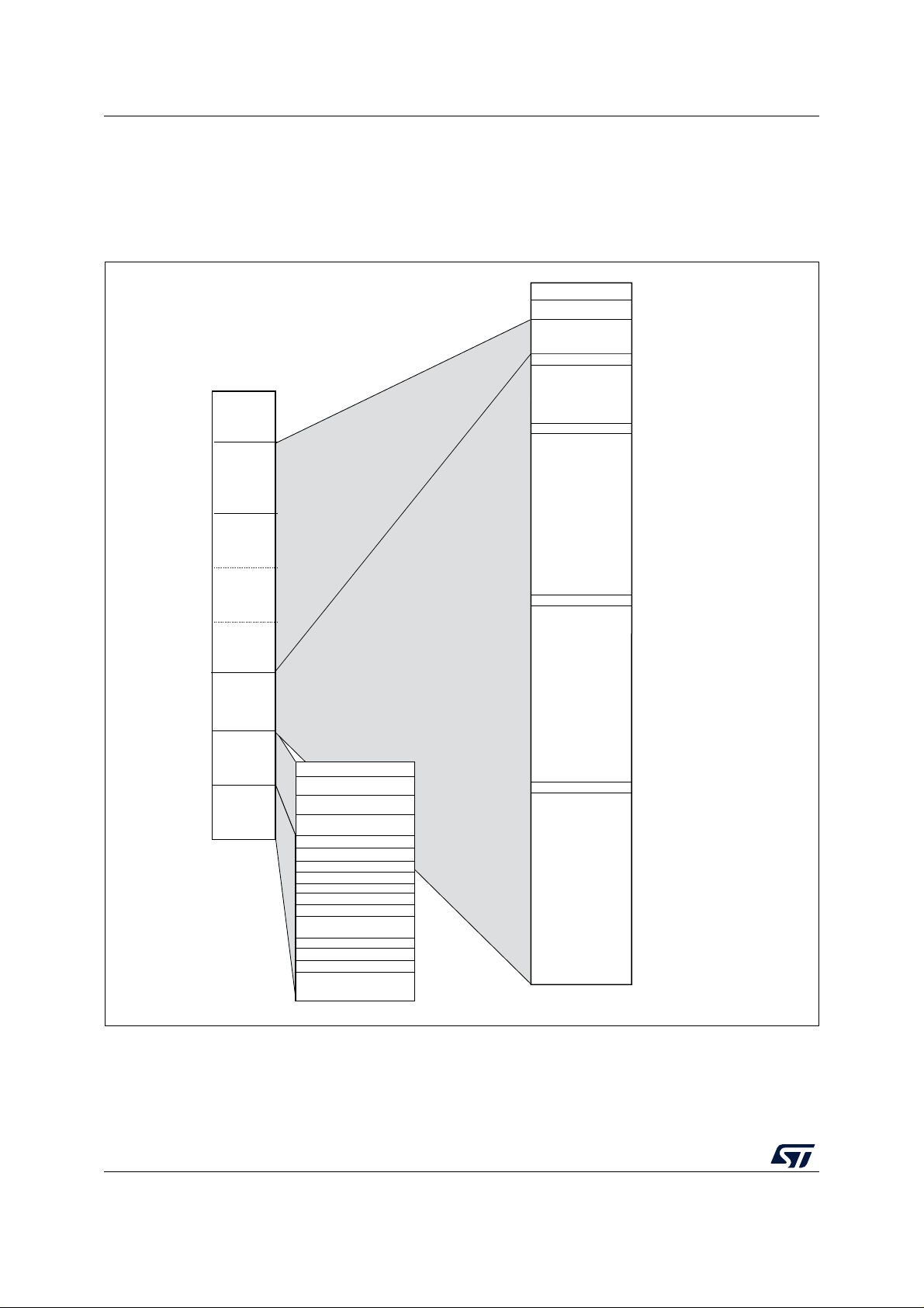
Memory mapping STM32F479xx
MSv33863V2
512-Mbyte
Block 7
Cortex
®
-4
Internal
peripherals
512-Mbyte
Block 6
FMC
0x0000 0000
0x1FFF FFFF
0x2000 0000
0x3FFF FFFF
0x4000 0000
0x5FFF FFFF
0x6000 0000
0x7FFF FFFF
0x8000 0000
0x9FFF FFFF
0xA000 0000
0xCFFF FFFF
0xD000 0000
0xDFFF FFFF
0xE000 0000
0xFFFF FFFF
Reserved
0x2000 0000 - 0x2002 7FFF
0x2002 8000 - 0x2002 FFFF
0x2005 0000 - 0x3FFF FFFF
0x4000 0000
Reserved
0x4000 7FFF
0x4000 8000 - 0x4000 FFFF
0x4001 0000
Reserved
0x5006 0C00 - 0x5FFF FFFF
AHB3
0x6000 0000 - 0xDFFF FFFF
AHB2
0x5006 0BFF
0x5000 0000
SRAM3
(128 KB aliased by bit-banding)
0x2003 0000 - 0x2004 FFFF
APB1
APB2
0x4001 73FF
0x4001 7400 - 0x4001 FFFF
Reserved
0x4008 0000 - 0x4FFF FFFF
0x4007 FFFF
AHB1
Reserved
Flash memory
0x0820 0000 - 0x0FFF FFFF
0x1FFF 0000 - 0x1FFF 7A0F
0x1FFF C000 - 0x1FFF C00 F
0x0800 0000 - 0x081F FFFF
0x0020 0000 - 0x07FF FFFF
0x0000 0000 - 0x001F FFFF
System memory
Reserved
Reserved
Aliased to Flash, system
memory or SRAM depending
on the BOOT pins
0x1FFF C008 - 0x1FFF FFFF
0x1FFF 7A10 - 0x1FFF 7FFF
CCM data RAM
(64 KB data SRAM)
0x1000 0000 - 0x1000 FFFF
0x1001 0000 - 0x1FFE BFFF
0x1FFE C000 - 0x1FFE C00 F
Option bytes
Reserved
0x1FFE C008 - 0x1FFE FFFF
0x4002 0000
Cortex
®
-M4
internal peripheral
0xE000 0000 - 0xE00F FFFF
Reserved
0xE010 0000 - 0xFFFF FFFF
512-Mbyte
Block 5
FMC and
QUADSPI
512-Mbyte
Block 4
FMC bank3 and
QUADSPI bank
512-Mbyte
Block 3
FMC bank1 to
QUADSPI bank 2
512-Mbyte
Block 2
Peripherals
512-Mbyte
Block 1
SRAM
512-Mbyte
Block 0
SRAM
SRAM2
(32 KB aliased by bit-banding)
SRAM1
(160 KB aliased by bit-banding)
Reserved
Option Bytes
Reserved
Reserved
4 Memory mapping
The memory map is shown in Figure 21.
Figure 21. Memory map
84 /22 0 DS 1111 8 Rev 6
Page 85
STM32F479xx Memory mapping
Table 13. STM32F479xx register boundary addresses
(1)
Bus Boundary address Peripheral
- 0xE00F FFFF - 0xFFFF FFFF Reserved
®
Cortex
-M4 0xE000 0000 - 0xE00F FFFF Cortex®-M4 internal peripherals
0xD000 0000 - 0xDFFF FFFF FMC bank 6
0xC000 0000 - 0xCFFF FFFF FMC bank 5
0xA000 1000 - 0xA0001FFF Quad-SPI control register
0xA000 2000 - 0xBFFF FFFF Reserved
AHB3
0xA000 0000- 0xA000 0FFF FMC control register
0x9000 0000 - 0x9FFF FFFF Quad-SPI bank
0x8000 0000 - 0x8FFF FFFF FMC bank 3
0x7000 0000 - 0x7FFF FFFF FMC bank 2 (reserved)
0x6000 0000 - 0x6FFF FFFF FMC bank 1
- 0x5006 0C00- 0x5FFF FFFF Reserved
0x5006 0800 - 0x5006 0BFF RNG
0x5006 0400 - 0x5006 07FF HASH
0x5006 0000 - 0x5006 03FF CRYP
AHB2
0x5005 0400 - 0x5005 FFFF Reserved
0x5005 0000 - 0x5005 03FF DCMI
0x5004 0000- 0x5004 FFFF Reserved
0x5000 0000 - 0x5003 FFFF USB OTG FS
DS 1111 8 Rev 6 85/ 2 2 0
88
Page 86

Memory mapping STM32F479xx
Table 13. STM32F479xx register boundary addresses
Bus Boundary address Peripheral
- 0x4008 0000- 0x4FFF FFFF Reserved
0x4004 0000 - 0x4007 FFFF USB OTG HS
0x4002 BC00- 0x4003 FFFF Reserved
0x4002 B000 - 0x4002 BBFF Chrom (DMA2D)
0x4002 9400 - 0x4002 AFFF Reserved
0x4002 9000 - 0x4002 93FF
0x4002 8C00 - 0x4002 8FFF
0x4002 8800 - 0x4002 8BFF
0x4002 8400 - 0x4002 87FF
0x4002 8000 - 0x4002 83FF
0x4002 6800 - 0x4002 7FFF Reserved
0x4002 6400 - 0x4002 67FF DMA2
0x4002 6000 - 0x4002 63FF DMA1
0x4002 5000 - 0x4002 5FFF Reserved
0x4002 4000 - 0x4002 4FFF BKPSRAM
ETHERNET MAC
(1)
(continued)
AHB1
0x4002 3C00 - 0x4002 3FFF Flash interface register
0x4002 3800 - 0x4002 3BFF RCC
0x4002 3400 - 0x4002 37FF Reserved
0x4002 3000 - 0x4002 33FF CRC
0x4002 2C00 - 0x4002 2FFF Reserved
0x4002 2800 - 0x4002 2BFF GPIOK
0x4002 2400 - 0x4002 27FF GPIOJ
0x4002 2000 - 0x4002 23FF GPIOI
0x4002 1C00 - 0x4002 1FFF GPIOH
0x4002 1800 - 0x4002 1BFF GPIOG
0x4002 1400 - 0x4002 17FF GPIOF
0x4002 1000 - 0x4002 13FF GPIOE
0x4002 0C00 - 0x4002 0FFF GPIOD
0x4002 0800 - 0x4002 0BFF GPIOC
0x4002 0400 - 0x4002 07FF GPIOB
0x4002 0000 - 0x4002 03FF GPIOA
86 /22 0 DS 1111 8 Rev 6
Page 87
STM32F479xx Memory mapping
Table 13. STM32F479xx register boundary addresses
(1)
(continued)
Bus Boundary address Peripheral
0x4001 7400 - 0x4001 FFFF Reserved
0x4001 6C00 - 0x4001 73FF DSI Host
0x4001 6800 - 0x4001 6BFF LCD-TFT
0x4001 5C00 - 0x4001 67FF Reserved
0x4001 5800 - 0x4001 5BFF SAI1
0x4001 5400 - 0x4001 57FF SPI6
0x4001 5000 - 0x4001 53FF SPI5
0x4001 4C00 - 0x4001 4FFF Reserved
0x4001 4800 - 0x4001 4BFF TIM11
0x4001 4400 - 0x4001 47FF TIM10
0x4001 4000 - 0x4001 43FF TIM9
0x4001 3C00 - 0x4001 3FFF EXTI
APB2
0x4001 3800 - 0x4001 3BFF SYSCFG
0x4001 3400 - 0x4001 37FF SPI4
0x4001 3000 - 0x4001 33FF SPI1
0x4001 2C00 - 0x4001 2FFF SDIO
0x4001 2400 - 0x4001 2BFF Reserved
0x4001 2000 - 0x4001 23FF ADC1 - ADC2 - ADC3
0x4001 1800 - 0x4001 1FFF Reserved
0x4001 1400 - 0x4001 17FF USART6
0x4001 1000 - 0x4001 13FF USART1
0x4001 0800 - 0x4001 0FFF Reserved
0x4001 0400 - 0x4001 07FF TIM8
0x4001 0000 - 0x4001 03FF TIM1
DS 1111 8 Rev 6 87/ 2 2 0
88
Page 88
Memory mapping STM32F479xx
Table 13. STM32F479xx register boundary addresses
Bus Boundary address Peripheral
- 0x4000 8000- 0x4000 FFFF Reserved
0x4000 7C00 - 0x4000 7FFF UART8
0x4000 7800 - 0x4000 7BFF UART7
0x4000 7400 - 0x4000 77FF DAC
0x4000 7000 - 0x4000 73FF PWR
0x4000 6C00 - 0x4000 6FFF Reserved
0x4000 6800 - 0x4000 6BFF CAN2
0x4000 6400 - 0x4000 67FF CAN1
0x4000 6000 - 0x4000 63FF Reserved
0x4000 5C00 - 0x4000 5FFF I2C3
0x4000 5800 - 0x4000 5BFF I2C2
0x4000 5400 - 0x4000 57FF I2C1
0x4000 5000 - 0x4000 53FF UART5
0x4000 4C00 - 0x4000 4FFF UART4
0x4000 4800 - 0x4000 4BFF USART3
(1)
(continued)
APB1
0x4000 4400 - 0x4000 47FF USART2
0x4000 4000 - 0x4000 43FF I2S3ext
0x4000 3C00 - 0x4000 3FFF SPI3 / I2S3
0x4000 3800 - 0x4000 3BFF SPI2 / I2S2
0x4000 3400 - 0x4000 37FF I2S2ext
0x4000 3000 - 0x4000 33FF IWDG
0x4000 2C00 - 0x4000 2FFF WWDG
0x4000 2800 - 0x4000 2BFF RTC & BKP Registers
0x4000 2400 - 0x4000 27FF Reserved
0x4000 2000 - 0x4000 23FF TIM14
0x4000 1C00 - 0x4000 1FFF TIM13
0x4000 1800 - 0x4000 1BFF TIM12
0x4000 1400 - 0x4000 17FF TIM7
0x4000 1000 - 0x4000 13FF TIM6
0x4000 0C00 - 0x4000 0FFF TIM5
0x4000 0800 - 0x4000 0BFF TIM4
0x4000 0400 - 0x4000 07FF TIM3
0x4000 0000 - 0x4000 03FF TIM2
1. The reserved boundary address are shown in grayed cells
88 /22 0 DS 1111 8 Rev 6
Page 89

STM32F479xx Electrical characteristics
5 Electrical characteristics
5.1 Parameter conditions
Unless otherwise specified, all voltages are referenced to VSS.
5.1.1 Minimum and maximum values
Unless otherwise specified the minimum and maximum values are guaranteed in the worst
conditions of ambient temperature, supply voltage and frequencies by tests in production on
100% of the devices with an ambient temperature at T
the selected temperature range).
Data based on characterization results, design simulation and/or technology characteristics
are indicated in the table footnotes and are not tested in production. Based on
characterization, the minimum and maximum values refer to sample tests and represent the
mean value plus or minus three times the standard deviation (mean±3σ).
5.1.2 Typical values
Unless otherwise specified, typical data are based on TA = 25 °C, VDD = 3.3 V (for the
1.7 V V
tested.
3.6 V voltage range). They are given only as design guidelines and are not
DD
= 25 °C and TA = TAmax (given by
A
Typical ADC accuracy values are determined by characterization of a batch of samples from
a standard diffusion lot over the full temperature range, where 95% of the devices have an
error less than or equal to the value indicated
5.1.3 Typical curves
Unless otherwise specified, all typical curves are given only as design guidelines and are
not tested.
5.1.4 Loading capacitor
The loading conditions used for pin parameter measurement are shown in Figure 22.
5.1.5 Pin input voltage
The input voltage measurement on a pin of the device is described in Figure 23.
Figure 22. Pin loading conditions Figure 23. Pin input voltage
C = 50 pF
MCU pin
(mean±2σ).
MCU pin
V
IN
MS19011V2
DS 1111 8 Rev 6 89/ 2 2 0
MS19010V2
191
Page 90

Electrical characteristics STM32F479xx
MS38256V1
Backup circuitry
(OSC32K,RTC,
Wakeup logic
Backup registers,
backup RAM)
Kernel logic
(CPU, digital
& RAM)
Analog:
RCs, PLL,..
Power
switch
V
BAT
GPIOs
OUT
IN
20 × 100 nF
+ 1 × 4.7 μF
V
BAT
= 1.65 to 3.6 V
Voltage
regulator
V
DDA
ADC
Level shifter
IO
Logic
V
DD
100 nF
+ 1 μF
Flash memory
V
CAP_1
V
CAP_2
2 × 2.2 μF
BYPASS_REG
PDR_ON
Reset
controller
V
DD
1/2/...19/20
V
SS
1/2/...19/20
V
DD
V
REF+
V
REF-
V
SSA
V
REF
100 nF
+ 1 μF
OTG-FS
PHY
V
DDUSB
100 nF
V
DDUSB
DSI
PHY
DSI
Voltage
regulator
V
DDDSI
V
CAPDSI
V
DD12DSI
V
SSDSI
2.2 μF
5.1.6 Power supply scheme
Figure 24. Power supply scheme
1. To connect BYPASS_REG and PDR_ON pins, refer to Section 2.19 and Section 2.20.
2. The two 2.2 µF ceramic capacitors on V
Caution: Each power supply pair (VDD/VSS, V
capacitors when the voltage regulator is OFF.
3. The 4.7 µF ceramic capacitor must be connected to one of the V
DDA
and V
4. V
capacitors as shown above. These capacitors must be placed as close as possible to, or
must be connected to VDD and VSS, respectively.
SSA
below, the appropriate pins on the underside of the PCB to ensure good operation of the
device. It is not recommended to remove filtering capacitors to reduce PCB size or cost.
This might cause incorrect operation of the device.
CAP_1
DDA/VSSA
and V
should be replaced by two 100 nF decoupling
CAP_2
pin.
DD
...) must be decoupled with filtering ceramic
90 /22 0 DS 1111 8 Rev 6
Page 91

STM32F479xx Electrical characteristics
ai14126
V
BAT
V
DD
V
DDA
IDD_V
BAT
I
DD
5.1.7 Current consumption measurement
Figure 25. Current consumption measurement scheme
5.2 Absolute maximum ratings
Stresses above the absolute maximum ratings listed in Tab le 14 , Table 15, and Tabl e 16
may cause permanent damage to the device. These are stress ratings only and functional
operation of the device at these conditions is not implied. Exposure to maximum rating
conditions for extended periods may affect device reliability.
Table 14. Voltage characteristics
Symbol Ratings Min Max Unit
V
DD–VSS
External main supply voltage
(including V
Input voltage on FT pins
DDA, VDD, VDDUSB, VDDDSI
(2)
and V
BAT
(1)
)
Input voltage on TTa pins V
V
IN
Input voltage on any other pin V
Input voltage on BOOT pin V
| Variations between different VDD power pins - 50
|V
DDx
|V
SSX VSS
V
ESD(HBM)
1. All main power (VDD, V
the external power supply, in the permitted range.
2. VIN maximum value must always be respected. Refer to Ta bl e 1 5 for the values of the maximum allowed
injected current.
3. Including V
| Variations between all the different ground pins
Electrostatic discharge voltage (human body model) see Section 5.3.18
REF-
pin
DDA
, V
DDUSB
, V
) and ground (VSS, V
DDDSI
(3)
) pins must always be connected to
SSA
− 0.3 4.0
VSS− 0.3 VDD+4.0
− 0.3 4.0
SS
− 0.3 4.0
SS
SS
9.0
-50
V
mV
DS 1111 8 Rev 6 91/ 2 2 0
191
Page 92

Electrical characteristics STM32F479xx
Table 15. Current characteristics
Symbol Ratings Max. Unit
(1)
(1)
(1)
(1)
290
− 290
100
− 100
I
I
I
VDDUSB
I
I
VDD
VSS
VDD
VSS
Total current into sum of all V
DD_x
Total current out of sum of all V
Total current into V
Maximum current into each V
power line (source) 25
DDUSB
DD_x
Maximum current out of each V
power lines (source)
ground lines (sink)
SS_x
power line (source)
ground line (sink)
SS_x
Output current sunk by any I/O and control pin 25
I
IO
I
IO
I
INJ(PIN)
I
INJ(PIN)
1. All main power (VDD, V
supply, in the permitted range.
2. This current consumption must be correctly distributed over all I/Os and control pins. The total output
current must not be sunk/sourced between two consecutive power supply pins referring to high pin count
LQFP packages.
3. Negative injection disturbs the analog performance of the device. See note in Section 5.3.24.
4. Positive injection is not possible on these I/Os and does not occur for input voltages lower than the
specified maximum value.
5. A positive injection is induced by VIN>V
never be exceeded. Refer to Table 14 for the values of the maximum allowed input voltage.
6. When several inputs are submitted to a current injection, the maximum ΣI
positive and negative injected currents (instantaneous values).
Output current sourced by any I/Os and control pin − 25
Total output current sunk by sum of all I/O and control pins
(2)
Total output current sunk by sum of all USB I/Os 25
Total output current sourced by sum of all I/Os and control pins
Injected current on FT pins
(3)
Injected current on NRST and BOOT0 pins
Injected current on TTa pins
(5)
Total injected current (sum of all I/O and control pins)
) and ground (VSS, V
DDA
(4)
(4)
(5)
(6)
) pins must always be connected to the external power
SSA
while a negative injection is induced by VIN<VSS. I
DDA
is the absolute sum of the
INJ(PIN)
(2)
120
− 120
− 5/+0
±5
±25
INJ(PIN)
mA
must
Table 16. Thermal characteristics
Symbol Ratings Value Unit
T
STG
T
J
Storage temperature range − 65 to +150 °C
Maximum junction temperature 125 °C
92 /22 0 DS 1111 8 Rev 6
Page 93

STM32F479xx Electrical characteristics
5.3 Operating conditions
5.3.1 General operating conditions
Table 17. General operating conditions
Symbol Parameter Conditions
Power Scale 3 (VOS[1:0] bits in PWR_CR
register = 0x01),
Regulator ON, over-drive OFF
Power Scale 2 (VOS[1:0] bits
in PWR_CR register = 0x10),
f
HCLK
Internal AHB clock frequency
Regulator ON
Power Scale 1 (VOS[1:0] bits
in PWR_CR register= 0x11),
Regulator ON
Over-drive OFF 0 - 42
f
PCLK1
Internal APB1 clock frequency
Over-drive ON 0 - 45
Over-drive OFF 0 - 84
f
PCLK2
V
Internal APB2 clock frequency
Over-drive ON 0 - 90
Standard operating voltage - 1.7
DD
Analog operating voltage
V
DDA
Analog operating voltage
Must be the same potential as V
(ADC limited to 1.2 M samples)
(3)(4)
(ADC limited to 2.4 M samples)
V
DDUSB
V
DDDSI
V
BAT
USB supply voltage
(supply voltage for PA11, PA12,
PB14 and PB15 pins)
DSI system operating voltage - 1.7
Backup operating voltage - 1.65 - 3.6
USB not used 0 3.3 3.6
USB used 3.0 - 3.6
(1)
Over-drive
OFF
Over-drive
ON
Over-drive
OFF
Over-drive
ON
(5)
DD
Min Typ Max Unit
0-120
-144
0
-168
-168
MHz
0
-180
(2)
-3.6
(2)
1.7
-2.4
2.4 - 3.6
(2)
-3.6
V
DS 1111 8 Rev 6 93/ 2 2 0
191
Page 94

Electrical characteristics STM32F479xx
Table 17. General operating conditions (continued)
Symbol Parameter Conditions
Power Scale 3 ((VOS[1:0] bits in
PWR_CR register = 0x01), 120 MHz
HCLK max frequency
Power Scale 2 ((VOS[1:0] bits in
Regulator ON: 1.2 V internal
voltage on V
V
12
CAP_1/VCAP_2
PWR_CR register = 0x10), 144 MHz
HCLK max frequency with over-drive OFF
pins
or 168 MHz with over-drive ON
Power Scale 1 ((VOS[1:0] bits in
PWR_CR register = 0x11), 168 MHz
HCLK max frequency with over-drive OFF
or 180 MHz with over-drive ON
Regulator OFF: 1.2 V external
voltage must be supplied from
external regulator on
V
CAP_1/VCAP_2
Input voltage on RST and FT
(7)
pins
V
IN
Input voltage on TTa pins - − 0.3 -
pins
(6)
Max frequency 120 MHz 1.10 1.14 1.20
Max frequency 144 MHz 1.20 1.26 1.32
Max frequency 168 MHz 1.26 1.32 1.38
2V VDD 3.6 V − 0.3 - 5.5
2V − 0.3 - 5.2
V
DD
(1)
Min Typ Max Unit
1.08 1.14 1.20
1.20 1.26 1.32
V
1.26 1.32 1.40
V
DDA
V
+0.3
Input voltage on BOOT0 pin - 0 - 9
LQFP100 - - 465
LQFP144 - - 500
WLCSP168 - - 645
Power dissipation
P
at T
D
= 85 °C for suffix 6
A
or TA = 105 °C for suffix 7
UFBGA169 - - 385
(8)
LQFP176 - - 526
UFBGA176 - - 513
LQFP208 - - 1053
TFBGA216 - - 690
Ambient temperature for 6
suffix version
T
A
Ambient temperature for 7
suffix version
T
J Junction temperature range
Maximum power dissipation − 40 - 85
Low power dissipation
(9)
Maximum power dissipation − 40 - 105
Low power dissipation
(9)
6 suffix version − 40 - 105
7 suffix version − 40 - 125
1. The over-drive mode is not supported at the voltage ranges from 1.7 to 2.1 V.
2. V
3. When the ADC is used, refer to Table 76.
4. If V
5. It is recommended to power V
V
6. The over-drive mode is not supported when the internal regulator is OFF.
minimum value of 1.7 V is obtained with the use of an external power supply supervisor (refer to Section 2.19.2).
DD/VDDA
pin is present, it must respect the following condition: V
REF+
and V
can be tolerated during power-up and power-down operation.
DDA
DD
from the same source. A maximum difference of 300 mV between V
DDA
DDA-VREF+
< 1.2 V.
− 40 - 105
− 40 - 125
and
DD
mW
°C
94 /22 0 DS 1111 8 Rev 6
Page 95

STM32F479xx Electrical characteristics
MS19044V2
ESR
R
Leak
C
7. To sustain a voltage higher than VDD+0.3, the internal Pull-up and Pull-Down resistors must be disabled
8. If T
9. In low power dissipation state, T
is lower, higher PD values are allowed as long as TJ does not exceed T
A
can be extended to this range as long as TJ does not exceed T
A
Table 18. Limitations depending on the operating power supply range
Jmax
.
.
Jmax
Maximum Flash
Operating
power
supply range
=
V
DD
1.7 to 2.1 V
(3)
ADC
operation
memory access
frequency with
no wait states
(f
Flashmax
20 MHz
)
(4)
Conversion time
up to 1.2 Msps
=
V
DD
2.1 to 2.4 V
=
V
DD
2.4 to 2.7 V
22 MHz
24 MHz
Conversion time
up to 2.4 Msps
=
V
DD
2.7 to 3.6 V
1. Applicable only when the code is executed from Flash memory. When the code is executed from RAM, no wait state is
required.
2. Thanks to the ART accelerator and the 128-bit Flash memory, the number of wait states given here does not impact the
execution speed from Flash memory since the ART accelerator allows to achieve a performance equivalent to 0 wait state
program execution.
3. V
4. Prefetch is not available.
5. When V
electrical characteristics of D- and D+ pins will be degraded between 2.7 and 3 V.
(5)
minimum value of 1.7 V is obtained with the use of an external power supply supervisor (refer to Section 2.19.2).
DD/VDDA
is connected to VDD, the voltage range for USB full speed PHYs can drop down to 2.7 V. However the
DDUSB
30 MHz
Maximum HCLK
frequency
vs.
Flash memory wait
states
(1)(2)
168 MHz
with 8 wait states
and over-drive OFF
180 MHz
with 8 wait states
and over-drive ON
180 MHz
with 7 wait states
and over-drive ON
180 MHz
with 5 wait states
and over-drive ON
I/O operation
No I/O
compensation
I/O compensation
works
Possible Flash
memory
operations
8-bit erase
and program
operations only
16-bit erase
and program
operations
16-bit erase
and program
operations
32-bit erase
and program
operations
5.3.2 VCAP1/VCAP2 external capacitor
Stabilization for the main regulator is achieved by connecting an external capacitor C
the VCAP1/VCAP2 pins. C
1. Legend: ESR is the equivalent series resistance.
is specified in Tab le 1 9.
EXT
Figure 26. External capacitor C
DS 1111 8 Rev 6 95/ 2 2 0
EXT
EXT
to
191
Page 96
Electrical characteristics STM32F479xx
Table 19. VCAP1/VCAP2 operating conditions
(1)
Symbol Parameter Conditions
CEXT Capacitance of external capacitor 2.2 µF
ESR ESR of external capacitor < 2
1. When bypassing the voltage regulator, the two 2.2 µF V
replaced by two 100 nF decoupling capacitors.
capacitors are not required and should be
CAP
5.3.3 Operating conditions at power-up / power-down (regulator ON)
Subject to general operating conditions for TA.
Table 20. Operating conditions at power-up / power-down (regulator ON)
Symbol Parameter Min Max Unit
t
VDD
VDD rise time rate 20
fall time rate 20
V
DD
5.3.4 Operating conditions at power-up / power-down (regulator OFF)
Subject to general operating conditions for TA.
Table 21. Operating conditions at power-up / power-down (regulator OFF)
µs/V
(1)
Symbol Parameter Conditions Min Max Unit
VDD rise time rate Power-up 20
t
VDD
t
VCAP
1. To reset the internal logic at power-down, a reset must be applied on pin PA0 when V
1.08 V.
V
fall time rate Power-down 20
DD
V
CAP_1
V
CAP_1
and V
and V
rise time rate Power-up 20
CAP_2
fall time rate Power-down 20
CAP_2
5.3.5 Reset and power control block characteristics
The parameters given in Tab le 22 are derived from tests performed under ambient
temperature and V
supply voltage conditions summarized in Tabl e 17 .
DD
reach below
DD
µs/V
96 /22 0 DS 1111 8 Rev 6
Page 97
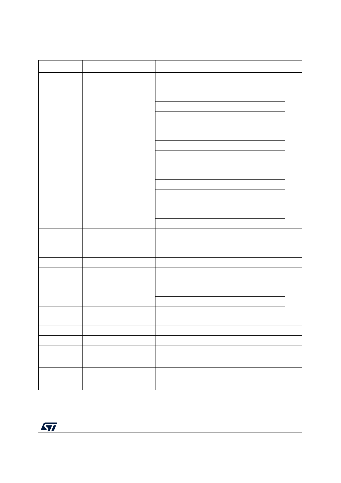
STM32F479xx Electrical characteristics
Table 22. Reset and power control block characteristics
Symbol Parameter Conditions Min Typ Max Unit
PLS[2:0]=000 (rising edge) 2.09 2.14 2.19
PLS[2:0]=000 (falling edge) 1.98 2.04 2.08
PLS[2:0]=001 (rising edge) 2.23 2.30 2.37
PLS[2:0]=001 (falling edge) 2.13 2.19 2.25
PLS[2:0]=010 (rising edge) 2.39 2.45 2.51
PLS[2:0]=010 (falling edge) 2.29 2.35 2.39
PLS[2:0]=011 (rising edge) 2.54 2.60 2.65
V
PVD
Programmable voltage
detector level selection
PLS[2:0]=011 (falling edge) 2.44 2.51 2.56
PLS[2:0]=100 (rising edge) 2.70 2.76 2.82
PLS[2:0]=100 (falling edge) 2.59 2.66 2.71
PLS[2:0]=101 (rising edge) 2.86 2.93 2.99
PLS[2:0]=101 (falling edge) 2.65 2.84 2.92
PLS[2:0]=110 (rising edge) 2.96 3.03 3.10
PLS[2:0]=110 (falling edge) 2.85 2.93 2.99
PLS[2:0]=111 (rising edge) 3.07 3.14 3.21
PLS[2:0]=111 (falling edge) 2.95 3.03 3.09
(1)
V
PVDhyst
V
POR/PDR
V
PDRhyst
PVD hysteresis - - 100 - mV
Power-on/power-down
reset threshold
(1)
PDR hysteresis - - 40 - mV
Falling edge 1.60 1.68 1.76
Rising edge 1.64 1.72 1.80
Falling edge 2.13 2.19 2.24
V
BOR1
Brownout level 1 threshold
Rising edge 2.23 2.29 2.33
Falling edge 2.44 2.50 2.56
V
BOR2
Brownout level 2 threshold
Rising edge 2.53 2.59 2.63
Falling edge 2.75 2.83 2.88
V
BOR3
V
BORhyst
T
RSTTEMPO
I
RUSH
(1)
Brownout level 3 threshold
Rising edge 2.85 2.92 2.97
(1)
BOR hysteresis - - 100 - mV
(1)(2)
POR reset temporization - 0.5 1.5 3.0 ms
InRush current on voltage
regulator power-on (POR or
- - 160 200 mA
wakeup from Standby)
InRush energy on voltage
regulator power-on (POR or
E
RUSH
(1)
wakeup from Standby)
1. Guaranteed by design.
2. The reset temporization is measured from the power-on (POR reset or wakeup from V
instruction is read by the user application code.
= 1.7 V, TA = 105 °C,
V
DD
I
= 171 mA for 31 µs
RUSH
--5.4µC
) to the instant when first
BAT
V
V
V
DS 1111 8 Rev 6 97/ 2 2 0
191
Page 98

Electrical characteristics STM32F479xx
5.3.6 Over-drive switching characteristics
When the over-drive mode switches from enabled to disabled or disabled to enabled, the
system clock is stalled during the internal voltage set-up.
The over-drive switching characteristics are given in Tab le 23 . They are subject to general
operating conditions for T
Symbol Parameter Conditions Min Typ Max Unit
Table 23. Over-drive switching characteristics
.
A
(1)
HSI - 45 -
T
od_swen
T
od_swdis
1. Guaranteed by design.
Over_drive switch
enable time
Over_drive switch
disable time
HSE max for 4 MHz
and min for 26 MHz
External HSE
50 MHz
HSI - 20 -
HSE max for 4 MHz
and min for 26 MHz.
External HSE
50 MHz
5.3.7 Supply current characteristics
The current consumption is a function of several parameters and factors such as the
operating voltage, ambient temperature, I/O pin loading, device software configuration,
operating frequencies, I/O pin switching rate, program location in memory and executed
binary code.
The current consumption is measured as described in Figure 25.
All the run-mode current consumption measurements given in this section are performed
with a reduced code that gives a consumption equivalent to CoreMark
45 - 100
- 40 -
20 - 80
- 15 -
®
code.
µs
98 /22 0 DS 1111 8 Rev 6
Page 99

STM32F479xx Electrical characteristics
Typical and maximum current consumption
The MCU is placed under the following conditions:
All I/O pins are in input mode with a static value at V
All peripherals are disabled except if it is explicitly mentioned.
The Flash memory access time is adjusted both to f
(see Table 18: Limitations depending on the operating power supply range).
When the regulator is OFF, the V
is provided externally, as described in Table 17:
12
General operating conditions.
The voltage scaling and over-drive mode are adjusted to f
– Scale 3 for f
– Scale 2 for 120 MHz < f
– Scale 1 for 144 MHz < f
The system clock is HCLK, f
120 MHz
HCLK
144 MHz
HCLK
180 MHz. The over-drive is only ON at 180 MHz.
HCLK
PCLK1
= f
HCLK
/4, and f
External clock frequency is 25 MHz and PLL is ON when f
The typical current consumption values are obtained for 1.7 V
range and for ambient temperature T
The maximum values are obtained for 1.7 V
maximum ambient temperature (T
For the voltage range 1.7 V
V
= 25 °C unless otherwise specified.
A
V
), unless otherwise specified.
A
2.1 V the maximum frequency is 168 MHz.
DD
or VSS (no load).
DD
frequency and V
HCLK
frequency as follows:
HCLK
= f
PCLK2
3.6 V voltage range and a
DD
/2.
HCLK
is higher than 25 MHz.
HCLK
V
DD
DD
3.6 V voltage
range
DS 1111 8 Rev 6 99/ 2 2 0
191
Page 100

Electrical characteristics STM32F479xx
Table 24. Typical and maximum current consumption in Run mode, code with data processing
running from Flash memory (ART accelerator enabled except prefetch) or RAM,
regulator ON
(1)
Max
Symbol Parameter Conditions f
All
peripherals
enabled
(2)(3)
Supply
I
DD
current in
Run mode
(MHz) Typ
HCLK
180 103 109
T
=
A
25 °C
(4)
TA =
85 °C
105 °C
142 175
TA =
(4)
168 94 99 124 149
150 84 89 114 140
144 77 81 104 127
120 57 60 79 98
90 43 46 64 84
60 30 33 51 70
30 16 19 37 57
25 14 16 34 54
16 7 10 28 48
8472646
4362444
2352343
180 50 56
(4)
89 124
(4)
168 45 51 75 102
150 41 46 70 97
Unit
mA
144 37 42 63 88
120 28 31 49 69
All
peripherals
disabled
(2)
90 21 24 42 63
60 15 17 36 56
30 9 11 29 49
25 7 10 28 48
16 4 7 25 45
8362244
4352343
2252343
1. Guaranteed based on test during characterization.
2. When analog peripheral blocks such as ADCs, DACs, HSE, LSE, HSI, or LSI are ON, an additional power consumption
should be considered.
3. When the ADC is ON (ADON bit set in the ADC_CR2 register), add an additional power consumption of 1.6 mA per ADC
for the analog part.
4. Guaranteed by test in production.
10 0 /220 DS 1111 8 Rev 6
 Loading...