

STMicroelectronics STM32F413H-DISCO Technical documentation - User Manual - A detailed description of board elements

Introduction
UM2135
User manual
Discovery kit with STM32F413ZH MCU
The 32F413HDISCOVERY Discovery kit is a complete demonstration and development
platform for the STMicroelectronics ARM
microcontroller. This microcontroller features up to 18 timers, internal 320-Kbyte SRAM,
1.5-Mbyte Flash memory and the following interfaces: four I2Cs, five I2Ss two of which are
full duplex, one SDIO, four USARTs, six UARTs, three CANs, one 12-bit ADC, two 12-bit
DACs, one SAI, six digital filters for Sigma Delta Modulator, twelve PDMs with stereo
microphone and beamforming support, one USB OTG FS, one FSMC interface, one QuadSPI interface and one SWD debugging support. The 32F413HDISCOVERY Discovery kit
offers everything required for users to get started quickly and develop applications easily.
The full range of hardware features of the 32F413HDISCOVERY Discovery kit helps users
to evaluate almost all peripherals (USB OTG FS, microSD
Audio DAC stereo with audio jack, ST-MEMS digital microphones, PSRAM, Quad-SPI Flash
memory, LCD parallel interface with capacitive multi-touch panel and others) and develop
applications. The Arduino
capabilities with a large choice of specialized add-on boards.The expansion connectors
allow easy connection of a daughterboard for specific customer applications. The integrated
ST-LINK/V2-1 provides an embedded in-circuit debugger and programmer for the STM32.
The 32F413HDISCOVERY Discovery kit comes with the comprehensive free software
libraries and examples available with the STM32Cube package.
Figure 1. 32F413HDISCOVERY board
™
Uno V3 connectivity support provides unlimited expansion
®
Cortex®-M4 core-based STM32F413ZHT6
™
card, Wi-Fi® 802.11 b/g/n, I2S
Figure 2. 32F413HDISCOVERY board
(Top view with LCD)
1. Pictures are not contractual.
April 2017 DocID029965 Rev 1 1/50
(Bottom view with STM32F413ZHT6)
www.st.com
1

Contents UM2135
Contents
1 Features . . . . . . . . . . . . . . . . . . . . . . . . . . . . . . . . . . . . . . . . . . . . . . . . . . . 6
2 Product marking . . . . . . . . . . . . . . . . . . . . . . . . . . . . . . . . . . . . . . . . . . . . 7
3 System requirements . . . . . . . . . . . . . . . . . . . . . . . . . . . . . . . . . . . . . . . . 7
4 Development toolchains . . . . . . . . . . . . . . . . . . . . . . . . . . . . . . . . . . . . . . 7
5 Demonstration software . . . . . . . . . . . . . . . . . . . . . . . . . . . . . . . . . . . . . . 7
6 Ordering information . . . . . . . . . . . . . . . . . . . . . . . . . . . . . . . . . . . . . . . . 8
7 Hardware layout and configuration . . . . . . . . . . . . . . . . . . . . . . . . . . . . . 9
7.1 32F413HDISCOVERY Discovery kit layout . . . . . . . . . . . . . . . . . . . . . . . 10
7.2 Embedded ST-LINK/V2-1 . . . . . . . . . . . . . . . . . . . . . . . . . . . . . . . . . . . . . .11
7.2.1 Drivers . . . . . . . . . . . . . . . . . . . . . . . . . . . . . . . . . . . . . . . . . . . . . . . . . . 12
7.2.2 ST-LINK/V2-1 firmware upgrade . . . . . . . . . . . . . . . . . . . . . . . . . . . . . . 12
7.2.3 Power supply . . . . . . . . . . . . . . . . . . . . . . . . . . . . . . . . . . . . . . . . . . . . . 12
7.3 Programming/debugging when the power supply
is not from ST-LINK/V2-1 . . . . . . . . . . . . . . . . . . . . . . . . . . . . . . . . . . . . . 14
7.4 Clock sources . . . . . . . . . . . . . . . . . . . . . . . . . . . . . . . . . . . . . . . . . . . . . . 15
7.5 Reset sources . . . . . . . . . . . . . . . . . . . . . . . . . . . . . . . . . . . . . . . . . . . . . 15
7.6 Audio . . . . . . . . . . . . . . . . . . . . . . . . . . . . . . . . . . . . . . . . . . . . . . . . . . . . 15
7.7 USB OTG FS . . . . . . . . . . . . . . . . . . . . . . . . . . . . . . . . . . . . . . . . . . . . . . 16
7.8 microSD card . . . . . . . . . . . . . . . . . . . . . . . . . . . . . . . . . . . . . . . . . . . . . . 16
7.9 PSRAM memory . . . . . . . . . . . . . . . . . . . . . . . . . . . . . . . . . . . . . . . . . . . . 16
7.10 Quad-SPI NOR Flash memory . . . . . . . . . . . . . . . . . . . . . . . . . . . . . . . . . 16
7.11 Virtual COM port . . . . . . . . . . . . . . . . . . . . . . . . . . . . . . . . . . . . . . . . . . . . 16
7.12 LCD . . . . . . . . . . . . . . . . . . . . . . . . . . . . . . . . . . . . . . . . . . . . . . . . . . . . . 17
7.13 Capacitive control touch panel . . . . . . . . . . . . . . . . . . . . . . . . . . . . . . . . . 17
7.14 Wi-Fi 802.11 b/g/n module . . . . . . . . . . . . . . . . . . . . . . . . . . . . . . . . . . . . 17
7.15 Buttons and LEDs . . . . . . . . . . . . . . . . . . . . . . . . . . . . . . . . . . . . . . . . . . 18
8 Connectors . . . . . . . . . . . . . . . . . . . . . . . . . . . . . . . . . . . . . . . . . . . . . . . 19
2/50 DocID029965 Rev 1

UM2135 Contents
8.1 Arduino Uno V3 connectors . . . . . . . . . . . . . . . . . . . . . . . . . . . . . . . . . . . 19
8.2 USB OTG FS Micro-AB connector CN17 . . . . . . . . . . . . . . . . . . . . . . . . 21
8.3 LCD FRIDA connector CN16 . . . . . . . . . . . . . . . . . . . . . . . . . . . . . . . . . . 22
8.4 Touch panel connector CN10 . . . . . . . . . . . . . . . . . . . . . . . . . . . . . . . . . . 23
8.5 microSD connector CN1 . . . . . . . . . . . . . . . . . . . . . . . . . . . . . . . . . . . . . . 24
8.6 ST-LINK/V2-1 USB Micro-AB connector CN2 . . . . . . . . . . . . . . . . . . . . . 25
8.7 TAG connector CN11 . . . . . . . . . . . . . . . . . . . . . . . . . . . . . . . . . . . . . . . . 26
8.8 Audio line output (green jack) connector CN5 . . . . . . . . . . . . . . . . . . . . . 27
8.9 Extension microphone connector CN12 . . . . . . . . . . . . . . . . . . . . . . . . . . 27
8.10 Optional audio stereo speakers CN3 and CN4 . . . . . . . . . . . . . . . . . . . . 28
Appendix A 32F413HDISCOVERY I/O assignment . . . . . . . . . . . . . . . . . . . . . . . 29
Appendix B Schematics. . . . . . . . . . . . . . . . . . . . . . . . . . . . . . . . . . . . . . . . . . . . . 34
Appendix C Federal Communications Commission (FCC)
and Industry Canada (IC) Compliance . . . . . . . . . . . . . . . . . . . . . . . 46
C.1 FCC Compliance Statement . . . . . . . . . . . . . . . . . . . . . . . . . . . . . . . . . . . 46
C.1.1 Part 15.19 . . . . . . . . . . . . . . . . . . . . . . . . . . . . . . . . . . . . . . . . . . . . . . . . 46
C.1.2 Part 15.105 . . . . . . . . . . . . . . . . . . . . . . . . . . . . . . . . . . . . . . . . . . . . . . . 46
C.1.3 Part 15.21 . . . . . . . . . . . . . . . . . . . . . . . . . . . . . . . . . . . . . . . . . . . . . . . . 46
C.2 IC Compliance Statement . . . . . . . . . . . . . . . . . . . . . . . . . . . . . . . . . . . . . 46
C.2.1 Compliance Statement . . . . . . . . . . . . . . . . . . . . . . . . . . . . . . . . . . . . . . 46
C.2.2 Déclaration de conformité. . . . . . . . . . . . . . . . . . . . . . . . . . . . . . . . . . . . 47
Appendix D CISPR32 . . . . . . . . . . . . . . . . . . . . . . . . . . . . . . . . . . . . . . . . . . . . . . . 48
D.1 Warning. . . . . . . . . . . . . . . . . . . . . . . . . . . . . . . . . . . . . . . . . . . . . . . . . . . 48
Revision history . . . . . . . . . . . . . . . . . . . . . . . . . . . . . . . . . . . . . . . . . . . . . . . . . . . . 49
DocID029965 Rev 1 3/50
3

List of tables UM2135
List of tables
Table 1. Ordering information . . . . . . . . . . . . . . . . . . . . . . . . . . . . . . . . . . . . . . . . . . . . . . . . . . . . . . . 8
Table 2. Assignment of the control ports to the LED indicators . . . . . . . . . . . . . . . . . . . . . . . . . . . . 18
Table 3. Pinout of the Arduino connector . . . . . . . . . . . . . . . . . . . . . . . . . . . . . . . . . . . . . . . . . . . . . 19
Table 4. USB OTG Micro-AB pinout (front view) . . . . . . . . . . . . . . . . . . . . . . . . . . . . . . . . . . . . . . . 21
Table 5. USB OTG FS power management . . . . . . . . . . . . . . . . . . . . . . . . . . . . . . . . . . . . . . . . . . . 21
Table 6. Pinout of the LCD connector. . . . . . . . . . . . . . . . . . . . . . . . . . . . . . . . . . . . . . . . . . . . . . . . 22
Table 7. Backlight power management . . . . . . . . . . . . . . . . . . . . . . . . . . . . . . . . . . . . . . . . . . . . . . 23
Table 8. Pinout of the touch panel . . . . . . . . . . . . . . . . . . . . . . . . . . . . . . . . . . . . . . . . . . . . . . . . . . 24
Table 9. Pinout of the microSD connector . . . . . . . . . . . . . . . . . . . . . . . . . . . . . . . . . . . . . . . . . . . . 25
Table 10. USB Micro-AB connector . . . . . . . . . . . . . . . . . . . . . . . . . . . . . . . . . . . . . . . . . . . . . . . . . . 26
Table 11. Pinout of the TAG connector . . . . . . . . . . . . . . . . . . . . . . . . . . . . . . . . . . . . . . . . . . . . . . . 26
Table 12. Audio jack connector . . . . . . . . . . . . . . . . . . . . . . . . . . . . . . . . . . . . . . . . . . . . . . . . . . . . . 27
Table 13. Extension microphone connector . . . . . . . . . . . . . . . . . . . . . . . . . . . . . . . . . . . . . . . . . . . . 28
Table 14. 32F413HDISCOVERY I/O assignment. . . . . . . . . . . . . . . . . . . . . . . . . . . . . . . . . . . . . . . . 29
Table 15. Document revision history . . . . . . . . . . . . . . . . . . . . . . . . . . . . . . . . . . . . . . . . . . . . . . . . . 49
4/50 DocID029965 Rev 1

UM2135 List of figures
List of figures
Figure 1. 32F413HDISCOVERY board . . . . . . . . . . . . . . . . . . . . . . . . . . . . . . . . . . . . . . . . . . . . . . . . 1
Figure 2. 32F413HDISCOVERY board . . . . . . . . . . . . . . . . . . . . . . . . . . . . . . . . . . . . . . . . . . . . . . . . 1
Figure 3. Hardware block diagram. . . . . . . . . . . . . . . . . . . . . . . . . . . . . . . . . . . . . . . . . . . . . . . . . . . . 9
Figure 4. 32F413HDISCOVERY Discovery kit (top side). . . . . . . . . . . . . . . . . . . . . . . . . . . . . . . . . . 10
Figure 5. 32F413HDISCOVERY Discovery kit (bottom side). . . . . . . . . . . . . . . . . . . . . . . . . . . . . . . 11
Figure 6. USB composite device . . . . . . . . . . . . . . . . . . . . . . . . . . . . . . . . . . . . . . . . . . . . . . . . . . . . 12
Figure 7. JP3: 5V_ST_LINK selection . . . . . . . . . . . . . . . . . . . . . . . . . . . . . . . . . . . . . . . . . . . . . . . . 13
Figure 8. JP3: 5V_ARD selection from CN7 (VIN_5V_ARD). . . . . . . . . . . . . . . . . . . . . . . . . . . . . . . 13
Figure 9. JP3: 5V_USB_FS . . . . . . . . . . . . . . . . . . . . . . . . . . . . . . . . . . . . . . . . . . . . . . . . . . . . . . . . 13
Figure 10. JP3: 5V_USB_CHARGER selection. . . . . . . . . . . . . . . . . . . . . . . . . . . . . . . . . . . . . . . . . . 14
Figure 11. Wi-Fi module. . . . . . . . . . . . . . . . . . . . . . . . . . . . . . . . . . . . . . . . . . . . . . . . . . . . . . . . . . . . 17
Figure 12. Arduino connector (top view) . . . . . . . . . . . . . . . . . . . . . . . . . . . . . . . . . . . . . . . . . . . . . . . 19
Figure 13. USB OTG FS Micro-AB connector (front view). . . . . . . . . . . . . . . . . . . . . . . . . . . . . . . . . . 21
Figure 14. LCD connector . . . . . . . . . . . . . . . . . . . . . . . . . . . . . . . . . . . . . . . . . . . . . . . . . . . . . . . . . . 22
Figure 15. Touch panel connector pinout . . . . . . . . . . . . . . . . . . . . . . . . . . . . . . . . . . . . . . . . . . . . . . 23
Figure 16. microSD connector (front view) . . . . . . . . . . . . . . . . . . . . . . . . . . . . . . . . . . . . . . . . . . . . . 24
Figure 17. USB Micro-AB connector (front view) . . . . . . . . . . . . . . . . . . . . . . . . . . . . . . . . . . . . . . . . . 25
Figure 18. TAG connector . . . . . . . . . . . . . . . . . . . . . . . . . . . . . . . . . . . . . . . . . . . . . . . . . . . . . . . . . . 26
Figure 19. TC2050-IDC-NL cable . . . . . . . . . . . . . . . . . . . . . . . . . . . . . . . . . . . . . . . . . . . . . . . . . . . . 26
Figure 20. Audio jack connector (front view) . . . . . . . . . . . . . . . . . . . . . . . . . . . . . . . . . . . . . . . . . . . . 27
Figure 21. Extension microphone connector (front view). . . . . . . . . . . . . . . . . . . . . . . . . . . . . . . . . . . 28
Figure 22. Top . . . . . . . . . . . . . . . . . . . . . . . . . . . . . . . . . . . . . . . . . . . . . . . . . . . . . . . . . . . . . . . . . . . 35
Figure 23. MCU . . . . . . . . . . . . . . . . . . . . . . . . . . . . . . . . . . . . . . . . . . . . . . . . . . . . . . . . . . . . . . . . . . 36
Figure 24. PSRAM . . . . . . . . . . . . . . . . . . . . . . . . . . . . . . . . . . . . . . . . . . . . . . . . . . . . . . . . . . . . . . . . 37
Figure 25. Quad-SPI . . . . . . . . . . . . . . . . . . . . . . . . . . . . . . . . . . . . . . . . . . . . . . . . . . . . . . . . . . . . . . 38
Figure 26. Audio. . . . . . . . . . . . . . . . . . . . . . . . . . . . . . . . . . . . . . . . . . . . . . . . . . . . . . . . . . . . . . . . . . 39
Figure 27. LCD. . . . . . . . . . . . . . . . . . . . . . . . . . . . . . . . . . . . . . . . . . . . . . . . . . . . . . . . . . . . . . . . . . . 40
Figure 28. USB OTG FS . . . . . . . . . . . . . . . . . . . . . . . . . . . . . . . . . . . . . . . . . . . . . . . . . . . . . . . . . . . 41
Figure 29. Peripherals . . . . . . . . . . . . . . . . . . . . . . . . . . . . . . . . . . . . . . . . . . . . . . . . . . . . . . . . . . . . . 42
Figure 30. Arduino Uno V3 connector . . . . . . . . . . . . . . . . . . . . . . . . . . . . . . . . . . . . . . . . . . . . . . . . . 43
Figure 31. ST-LINK with support of SWD only. . . . . . . . . . . . . . . . . . . . . . . . . . . . . . . . . . . . . . . . . . . 44
Figure 32. Power . . . . . . . . . . . . . . . . . . . . . . . . . . . . . . . . . . . . . . . . . . . . . . . . . . . . . . . . . . . . . . . . . 45
DocID029965 Rev 1 5/50
5

Features UM2135
1 Features
• STM32F413ZHT6 microcontroller featuring 1.5 Mbytes of Flash memory and 320
Kbytes of
• 240x240-pixel TFT LCD with touch screen
• 8-Mbit PSRAM; 512K word x 16bits
• 128-Mbit Quad-SPI Flash memory
2
• I
S audio codec
• 2 on-board ST-MEMS microphones
• Integrated Wi-Fi
• 2 push-buttons (user and reset)
• 2 user LEDs: one green and one red
• Jack connector for Audio line with microphone input and stereo output
• Connector for microSD
• USB OTG FS with Micro-AB connector
• Expansion connectors:
– Audio daughterboard (5 ST-MEMS microphones)
– Arduino Uno V3
• Flexible power supply options:
–ST
• On-board ST-LINK/V2-1 debugger/programmer with USB re-enumeration capability:
mass storage, virtual COM port, debug port
• Comprehensive free software libraries and examples available with the STM32Cube
package
• Support of wide choice of Integrated Development Environments (IDEs) including
IAR
SRAM, in LQFP144 package
®
module compliant with 802.11 b/g/n
™
card
LI
NK USB V
™
, Keil®, GCC-based IDEs
or external sources
BUS
6/50 DocID029965 Rev 1

UM2135 Product marking
2 Product marking
Evaluation tools marked as "ES" or "E" are not yet qualified and therefore they are not ready
to be used as reference design or in production. Any consequences deriving from such
usage will not be at ST charge. In no event, ST will be liable for any customer usage of these
engineering sample tools as reference design or in production.
"E" or "ES" marking examples of location:
• On the targeted STM32 that is soldered on the board (for illustration of STM32 marking,
refer to the section “Package characteristics” of the STM32 datasheet at www.st.com).
• Next to the evaluation tool ordering part number, that is stuck or silk-screen printed on
the board.
3 System requirements
• Windows® OS (XP, 7, 8 and 10), Linux® or MacOS
• USB Type-A to Micro-B cable
4 Development toolchains
™
• ARM® Keil®: MDK-ARM
• IAR™: EWARM
• GCC-based IDEs: free SW4STM32 from AC6
(a)
(a)
5 Demonstration software
The demonstration software is preloaded in the STM32F413ZH Flash memory for easy
demonstration of the device peripherals in standalone mode. The latest versions of the
demonstration source code and associated documentation can be downloaded from the
www.st.com/stm32f4-discovery webpage.
a. On Windows® only.
DocID029965 Rev 1 7/50
49

Ordering information UM2135
6 Ordering information
To order the 32F413HDISCOVERY Discovery kit, refer to Tab le 1:
Order code Target STM32
STM32F413H-DISCO STM32F413ZHT6
Table 1. Ordering information
8/50 DocID029965 Rev 1
UM2135 Hardware layout and configuration
06Y9
670)=+7
26&B
6:'
93RZHU
6XSSO\
.+]&U\VWDO
67/,1.9
&DSDFLWLYH
7RXFK6FUHHQ
0XOWLSRLQWV
86%27*)60LFUR
$%FRQQHFWRU
27*)6
0ELW365$0
)60&
/&''6,FRQQHFWRU
463,463,)ODVK0E
9&3
8$57
$UGXLQR8QR9
FRQQHFWRUV
*3,2V
:L)LPRGXOH
EJQ
63,
0LFUR6'FDUG
FRQQHFWRU
6'00&
26&B,1
'DWD
$GGUHVV
0+]
FWUO
,&)03
*3,2
8VHU,QWHUIDFH
[/('V
8VHULQWHUIDFH
SXVKEXWWRQ567
DQG:DNHXS
*3,2
,
6
$XGLR'$&DQG
DPSOLILHU
6WHUHR-DFN
/LQH2XW
0LFB,1
')6'0
')6'0
([W670PRGXOH
8SWR
PLFURSKRQHV
6ZLWFK
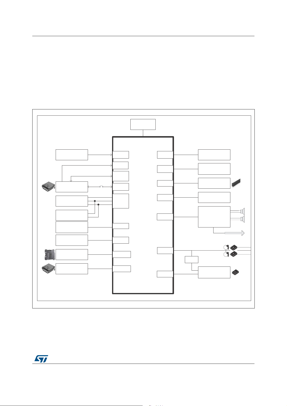
7 Hardware layout and configuration
The 32F413HDISCOVERY Discovery kit is designed around the STM32F413ZH (144-pin in
LQFP package). The hardware block diagram (see
between the STM32 and the peripherals (PSRAM, Quad-SPI Flash memory, LCD
connector, USB OTG connectors, USART, Audio, microSD
and embedded ST-LINK/V2-1). Refer to
Figure 4 and Figure 5 to locate these features on
the 32F413HDISCOVERY board.
Figure 3. Hardware block diagram
Figure 3) illustrates the connection
™
card, Arduino™ Uno V3 shields
DocID029965 Rev 1 9/50
49

Hardware layout and configuration UM2135
Arduino_D[8..15]: CN6
Arduino_D[0..7]: CN8
Arduino_A[0..5]: CN9
Arduino_PWR: CN7
PSRAM: U14
STLINK STM32: U6
Audio Mack: CN5
QSPI: U9
Audio Codec: U11
SD CARD: CN1
USB_STLINK: CN2
MEMS MP23: U1/U2
5V PWR: U3
3V PWR: U4
IDD JP: JP2
MCU_PWR: JP3
STM32F413ZHT6
7.1 32F413HDISCOVERY Discovery kit layout
Figure 4. 32F413HDISCOVERY Discovery kit (top side)
10/50 DocID029965 Rev 1

UM2135 Hardware layout and configuration
Touch screen CN10
MEMS MP34 U16/U17
LCD-PSRAM
Data probing CN15
Ext MEMS module
mb1299
ST-LINK UART CN13
User USB : CN17
CN16: LCD
connector
TAG footprint: CN11
User LED GREEN: LD3
User LED RED: LD4
LCD BackLight fct
LCD 240x240
5V PWR: LD6
ST-LINK LED: LD2
STLINK_DFU: CN14
ARD LED GREEN: LD5
User Elue %utton : B1
RESET black Button : B2
M1: Wi-Fi Module
Figure 5. 32F413HDISCOVERY Discovery kit (bottom side)
7.2 Embedded ST-LINK/V2-1
The ST-LINK/V2-1 programming and debugging tool is integrated on the
32F413HDISCOVERY Discovery kit. The new features supported on ST-LINK/V2-1 and not
present on ST-LINK/V2 are listed below:
• USB software re-enumeration
• Virtual COM port interface on USB
• Mass storage interface on USB
• USB power management request for more than 100 mA power on USB
These features are no more supported on ST-LINK/V2-1:
• SWIM interface
• Application voltage lower than 3 V
For all general information concerning debugging and programming features common
between V2 and V2-1 versions, refer to ST-LINK/V2 in-circuit debugger/programmer for
STM8 and STM32 User manual (UM1075) at the www.st.com website.
DocID029965 Rev 1 11/50
49

Hardware layout and configuration UM2135
7.2.1 Drivers
Before connecting the 32F413HDISCOVERY Discovery kit to a Windows® PC (XP, 7, 8 or
10) through a USB, a driver for the ST-LINK/V2-1 must be installed. It is available at the
www.st.com website.
In case the 32F413HDISCOVERY Discovery kit is connected to the PC before the driver is
installed, some 32F413HDISCOVERY interfaces may be declared as "unknown" in the PC
device manager. To recover from this situation the user must install the driver files, and
update the driver of the connected device from the device manager (see
Note: Prefer using the "USB Composite Device" handle for a full recovery.
Figure 6. USB composite device
Figure 6).
7.2.2 ST-LINK/V2-1 firmware upgrade
The ST-LINK/V2-1 embeds a firmware upgrade mechanism for in-situ upgrade through the
USB port. As the firmware may evolve during the life time of the ST-LINK/V2-1 product (for
example new functionalities, bug fixes, support for new microcontroller families), it is
recommended to visit www.st.com before starting to use the 32F413HDISCOVERY
Discovery kit and periodically, to stay up-to-date with the latest firmware version.
7.2.3 Power supply
The 32F413HDISCOVERY Discovery kit is designed to be powered by 5 V DC power
supply. It is possible to configure the 32F413HDISCOVERY board to use any of the
following four sources for the power supply:
• 5V_ST_LINK: DC power from USB ST-LINK connector.The power source is the USB
Micro-B connector of the ST-LINK/V2-1 (CN2). A jumper needs to be placed on pins 1
and 2 of JP3 (5V_ST_LINK on silkscreen) to enable this power source (see Figure 7). It
is the default setting. In this configuration only the ST-LINK MCU is powered before the
USB enumeration, because the host PC only provides 100 mA to the board at that
time. During the USB enumeration, the 32F413HDISCOVERY board asks for the
500 mA power to the host PC. If the host is able to provide the required power, the
enumeration succeeds and, the power transistor ST890 (U10) is switched ON, the
entire board is powered and the LED LD1 remains turned OFF, thus the
32F413HDISCOVERY board consumes up to 500 mA current, but no more. If the host
is not able to provide the requested current, the enumeration fails. Therefore the ST890
remains OFF and the MCU part including the extension board is not powered. As a
12/50 DocID029965 Rev 1

UM2135 Hardware layout and configuration
consequence the red LED LD1 is turned ON. In this case it is mandatory to use an
external power supply.
Figure 7. JP3: 5V_ST_LINK selection
• 5V_ARD: 7-12V DC power from Arduino Uno V3 connector. The power source is CN7
pin 8 named V
on Arduino connector silkscreen. A jumper needs to be placed on pins
IN
3 and 4 of JP3 (5V_ARD on silkscreen) to enable this power source (see Figure 8).
Figure 8. JP3: 5V_ARD selection from CN7 (VIN_5V_ARD)
• 5V_USB_FS: DC power from USB user connector.The power source is the USB Micro-
AB connector (CN17). In this case, the 32F413HDISCOVERY board is powered by an
external USB host without current limitation on board. A jumper needs to be placed on
pins 5 and 6 of JP3 (5V_USB_FS on silkscreen) to enable this power source (see
Figure 9).
Figure 9. JP3: 5V_USB_FS
DocID029965 Rev 1 13/50
49

Hardware layout and configuration UM2135
• 5V_USB_CHARGER: DC power charger from USB ST-LINK. The power source is the
USB Micro-B connector of the ST-LINK/V2-1 (CN2). In this case, if the
32F413HDISCOVERY Discovery kit is powered by an external USB charger the debug
is not available. If the PC is connected instead of the charger, the limitation is no more
effective, in this case the PC could be damaged. A jumper has to be placed on pins 7
and 8 of JP3 (5V_USB_CHARGER on silkscreen) to enable this power source (see
Figure 10).
Figure 10. JP3: 5V_USB_CHARGER selection
Note: In case the board is powered by a USB charger, there is no USB enumeration, so the led
LD1 remains set to OFF permanently and the board is not powered. In this specific case
only, the jumper JP3 should be set in position 7-8, to allow the board to be powered anyway.
Caution: Do not connect the PC to the ST-LINK (CN2) when R45 is soldered. The PC may be
damaged or the board may not be powered correctly.
STM32F413ZH IDD current measurement: JP2
The STM32F413ZH current measurement can be done on JP2. By default a jumper is
placed on JP2.
For current measurement configuration, the jumper on JP2 should be removed and an amp
meters should be place on JP2.
Note: The 32F413HDISCOVERY Discovery kit must be powered by a power supply unit or by an
auxiliary equipment complying with the standard EN-60950-1: 2006+A11/2009, and must be
Safety Extra Low Voltage (SELV) with limited power capability.
7.3 Programming/debugging when the power supply is not from ST-LINK/V2-1
It is mandatory to power the 32F413HDISCOVERY Discovery kit first using CN7 (VIN) or
CN17 (USB_FS_OTG), then connecting the USB cable to the PC. Proceeding this way
ensures that the enumeration succeeds thanks to the external power source.
The following power sequence procedure must be respected:
1. Connect the jumper JP3 on (5V_ARD) or (5V_USB_FS)
2. Connect the external power source to CN7 in case of an Arduino shield or CN17 in
case of an USB FS host interface
14/50 DocID029965 Rev 1

UM2135 Hardware layout and configuration
3. Check that the GREEN LED LD6 is turned ON
4. Connect the PC to USB connector CN2
If this order is not respected, the board may be powered by V
following risks may be encountered:
1. If more than 500 mA current is needed by the board, the PC may be damaged or
current can be limited by the PC. As a consequence the board is not powered correctly.
2. 500 mA is requested at the enumeration, so there is a risk that the request is rejected
and enumeration does not succeed if the PC cannot provide such current.
7.4 Clock sources
Three clock sources are described below:
• MCO, 8 MHz clock from ST-LINK MCU for the STM32F413ZHT6
• X2, 8 MHz oscillator for the STM32F413ZHT6
• X1, 32.768 KHz crystal for the STM32F413ZHT6 embedded RTC
7.5 Reset sources
The reset signal of the 32F413HDISCOVERY Discovery kit is active low and the reset
sources include:
• Reset button B2
• Arduino Uno V3 shield board from CN7
• Embedded ST-LINK/V2-1
first from ST-LINK, and the
BUS
7.6 Audio
An audio codec WM8994ECS/R from CIRRUS with four DACs and two ADCs is connected
to the I
shared with the touch panel of the FRIDA LCD.
• The analog-line output is connected to the DAC of WM8994ECS/R via audio jack CN5.
• The microphone input is connected from the audio jack to the input line of
• Two optional external speakers can be connected to WM8994ECS/R through CN3 for
• Two digital microphones (ST-MEMS microphone) MP34DT01TR-M are on
• The connector CN12 offers the possibility to connect a microphone module with up to
2
WM8994ECS/R
left speaker and through CN4 for right speaker.
32F413HDISCOVERY Discovery kit. They are connected to the digital input
microphones of the STM32F413ZH and are managed by the DFSDM functionality.
five ST-MEMS microphones (see Figure 26: Audio). They are connected to the digital
input microphones of the STM32F413ZH and are managed by the DFSDM
functionality.
S interface of the STM32F413ZH. It communicates with the STM32 via the I2C bus
DocID029965 Rev 1 15/50
49

Hardware layout and configuration UM2135
7.7 USB OTG FS
The 32F413HDISCOVERY Discovery kit supports the USB OTG FS communication via a
USB Micro-AB connector.
A USB power switch (U15) is also connected on V
green LED LD7 is lit when either:
• Power switch is ON and the 32F413HDISCOVERY works as a USB host
• V
The red LED LD8 is lit when an overcurrent occurs.
Note:1 When the 32F413HDISCOVERY board is powered by the ST-LINK, the OTG function
provides up to 100
Note:2 When the 32F413HDISCOVERY board is powered by an external power supply, the OTG
function can provide more than 100
Note:3 When the 32F413HDISCOVERY board is powered by an external power supply through the
USB FS connector (CN17), in device mode, do not use a PC as power source.
is powered by another USB host when the32F413HDISCOVERY works as a
BUS
USB device.
mA.
mA, according to the external power supply capability.
and provides power to CN17. The
BUS
7.8 microSD card
The 32F413HDISCOVERY Discovery kit supports the microSD card connected to the SDIO
port of the STM32F413ZH.
The microSD card has to be compatible with the MMC 4.1 specification, or with the microSD
card memory specification version 2.0
7.9 PSRAM memory
The 8-Mbit PSRAM (IS66WV51216EBLL-55BLI from ISSI: Integrated Silicon Solution Inc) is
connected to the FSMC interface of the STM32F413ZH. This memory is organize as 512K
words by 16 bits.
7.10 Quad-SPI NOR Flash memory
The 128-Mbit Quad-SPI NOR Flash memory (N25Q128A13EF840F from MICRON) is
connected to the Quad-SPI interface of the STM32F413ZH.
7.11 Virtual COM port
The serial interface USART6 is directly available as a virtual COM port of the PC connected
to the ST-LINK/V2-1 USB connector CN13. The virtual COM port settings are configured as:
• 115200 b/s
• 8 bits data
• no parity
• 1 stop bit
• no flow control
16/50 DocID029965 Rev 1

UM2135 Hardware layout and configuration
7.12 LCD
The 240x240-pixel TFT LCD (FRD154BP2902 from Frida) is connected to the FSMC data
interface of the STM32F413ZH.
It uses the Sitronix ST7789H2 controller for 262K-color and TFT-LCD graphic type. Display
data are stored into the on-chip display data RAM of 240x320x18 bits. It performs display
data RAM read/write operation with no external operation clock, to minimize power
consumption.
An external SRAM is also used to store display data.
LCD_RS signal is used to determine whether the bus is carrying data or control/command
registers.
7.13 Capacitive control touch panel
The Capacitive Control Touch Panel (Frida LS015GF614A) is controlled by the
STM32F413ZH through the I2CFMP shared with audio codec.
7.14 Wi-Fi 802.11 b/g/n module
A Wi-Fi module from INVENTEK Systems ISM43362_M3x_l44 is integrated in the
32F413HDISCOVERY Discovery kit (see
The Inventek ISM43362-M3G-L44 is an embedded (eS-WiFi) wireless Internet Connectivity
device. The Wi-Fi hardware module consists of an ARM
integrated antenna and a Broadcom Wi-Fi device.
The module is driven by an SPI interface enabling the connection to the STM32F413ZH.
The Wi-Fi module requires no operating system and has a completely integrated TCP/IP
stack that only requires AT commands to establish connectivity.
Figure 11. Wi-Fi module
Figure 11).
®
-M3 Cortex® host processor, an
DocID029965 Rev 1 17/50
49

Hardware layout and configuration UM2135
7.15 Buttons and LEDs
The black button B2 located on LCD side, is the reset of the microcontroller STM32F413ZH
(refer to the
When the button is depressed the logic state is "0", otherwise the logic state is "1".
The blue button B1, located on the LCD side, is available to be used as a digital input or as
alternate function Wake-up.
When the button is depressed the logic state is "1", otherwise the logic state is "0".
Two LEDs (LD4 red and LD3 green) located on the LCD side, are available for the user
(refer to the
high logic state "1" should be written in the corresponding GPIO register.
Tab le 2 gives the assignment of the control ports to the LED indicators.
Figure 4: 32F413HDISCOVERY Discovery kit (top side)).
Figure 5: 32F413HDISCOVERY Discovery kit (bottom side)). To light a LED a
Table 2. Assignment of the control ports to the LED indicators
LED Color Name Comment
B1 BLUE USER_B Alternate function Wake-up PA0
B2 BLACK RESET NRST
LD1 RED Fault Power Current upper than 750 mA
LD2 RED/GREEN ST-LINK COM Green when communication
LD3 GREEN LED2_GREEN PC5
LD4 RED LED1_RED PE3
LD5 GREEN ARDUINO PB12
LD6 GREEN 5 V Power 5 V available
LD7 GREEN V
LD8 RED V
OK 5 V USB available
BUS
OCRCR PG7
BUS
18/50 DocID029965 Rev 1

UM2135 Connectors
8 Connectors
8.1 Arduino Uno V3 connectors
CN6, CN7, CN8 and CN9 are female connectors compatible with Arduino Uno V3. Most
shields designed for Arduino Uno V3 are also supported by the 32F413HDISCOVERY
Discovery kit.
Since the I/Os of the STM32F413ZH microcontroller are 5 V tolerant, there is no issue for
Arduino compatibility.
Example for the connector references (see Figure 12):
• CN6: Fisher BL 1-10 G
• CN7: Fisher BL 1-8 G
• CN8: Fisher BL 1-8 G
• CN9: Fisher BL 1-6 G
Figure 12. Arduino connector (top view)
Connector Pin number Pin name Signal name STM32 pin Function
CN7
Table 3. Pinout of the Arduino connector
1NC - -
2 IOREF - 3.3 V reference
3 NRST NRST NRST RESET
4 3.3 V - 3.3 V input/output
5 5 V - 5 V output
6 GND - GND
7 GND - GND
8V
IN
DocID029965 Rev 1 19/50
- Power input
49

Connectors UM2135
Table 3. Pinout of the Arduino connector (continued)
Connector Pin number Pin name Signal name STM32 pin Function
1 A0 ADC PC0 ADC1_IN10
2 A1 ADC PA1 ADC1_IN1
CN9
3 A2 ADC PA2 ADC1_IN2
4 A3 ADC PA5 ADC1_IN5
5 A4 ADC PB1 ADC1_IN9
6 A5 ADC PC4 ADC1_IN14
10 SCL/D15 ARD_D15 PB10 I2C2_SCL
9 SDA/D14 ARD_D14 PB11 I2C2_SDA
CN6
CN8
8A
VDD
V
REF
-V
REF
7 GND - - Ground
6 SCK/D13 ARD_D13 PB12 SPI3_SCK
5 MISO/D12 ARD_D12 PB4 SPI3_MISO
4
PWM/MOSI/
D11
ARD_D11 PB5
3 PWM/CS/D10 ARD_D10 PA15
TIM3_CH2/SPI3_
MOSI
TIM2_CH1/SPI3_N
SS
2 PWM/D9 ARD_D9 PB8 TIM4_CH3
1 D8 ARD_D8 PA4 IO
8 D7 ARD_D7 PC13 IO
7 PWM/D6 ARD_D6 PB0 TIM3_CH3
6 PWM/D5 ARD_D5 PE6 TIM9_CH2
5 D4 ARD_D4 PB6 EXT_IT_6
4 PWM/D3 ARD_D3 PF10 TIM5_CH4
3 D2 ARD_D2 PG13 I/O
2 TX/D1 ARD_D1 PF7 UART7_TX
1 RW/D0 ARD_D0 PF6 UART7_RX
20/50 DocID029965 Rev 1

UM2135 Connectors
8.2 USB OTG FS Micro-AB connector CN17
Example of connector reference (see Figure 13):
• Molex 475900001
Figure 13. USB OTG FS Micro-AB connector (front view)
Connector
Table 4. USB OTG Micro-AB pinout (front view)
Pin
number
1V
Pin names Signal name STM32 pin Function
BUS
USB_OTG_5V_VBUS PA9
5V power and
detection
2 DM (D-) USB_OTG_FS_N PA11 USB diff pair M
CN15
3 DP (D+) USB_OTG_FS_P PA12 USB diff pair P
4 ID USB_OTG_FS_ID PA10 USB Identification
5GND - - GND
Table 5. USB OTG FS power management
Pin number Pin names Signal names STM32 pin Function
U12-3 FAULTn USB_OTG_FS_OVRCR PG7 Over Current IT
U12-4 ENn USB_OTG_FS_PWR_EN PG8 USB Power enable
DocID029965 Rev 1 21/50
49

Connectors UM2135
8.3 LCD FRIDA connector CN16
Example of connector reference (see Figure 14):
• Hirose FH26-29S-0.3SHW
Figure 14. LCD connector
Connector
CN16
Table 6. Pinout of the LCD connector
Pin
number
1 GND - - Ground
2 FMARK LCD_TE PB14 Tearing Effect
3 DB15 LCD-PSRAM_D15 PD10 FSMC_D15
4 DB14 LCD-PSRAM_D14 PD9 FSMC_D14
5 DB13 LCD-PSRAM_D13 PD8 FSMC_D13
6 DB12 LCD-PSRAM_D12 PE15 FSMC_D12
7 DB11 LCD-PSRAM_D11 PE14 FSMC_D11
8 DB10 LCD-PSRAM_D10 PE13 FSMC_D10
9 DB9 LCD-PSRAM_D9 PE12 FSMC_D9
10 DB8 LCD-PSRAM_D8 PE11 FSMC_D8
11 DB7 LCD-PSRAM_D7 PE13 FSMC_D7
12 DB6 LCD-PSRAM_D6 PE9 FSMC_D6
13 DB5 LCD-PSRAM_D5 PE8 FSMC_D5
14 DB4 LCD-PSRAM_D4 PE7 FSMC_D4
15 DB3 LCD-PSRAM_D3 PD1 FSMC_D3
16 DB2 LCD-PSRAM_D2 PD0 FSMC_D2
Pin name Signal name STM32 pin Function
17 DB1 LCD-PSRAM_D1 PD15 FSMC_D1
18 DB0 LCD-PSRAM_D0 PD14 FSMC_D0
19 /RD LCD-PSRAM_NOE PD4 FSMC_NOE
20 /WR LCD-PSRAM_NWE PD5 FSMC_NWE
21 RS LCD-RS_A0 PF0 FSMC_RS
22/50 DocID029965 Rev 1
UM2135 Connectors
Table 6. Pinout of the LCD connector (continued)
Connector
CN16
Pin
number
22 /CS LCD_NE3 PG10 FSMC_NE
23 RESET LCD-CTP_RST PB13 RESET
24 IM - - 8/16 bit mode select
25 IOVCC 3.3 V - Power
26 VCI 3.3 V - Power
27 GND GND - Ground
28 LEDA LEDA - LED anode
29 LEDK LEDK - LED cathode
Pin name Signal name STM32 pin Function
The Tabl e 7 shows LCD connection for Backlight management:
Pin number Pin name Signal name STM32 pin Function
U18-7 EN LCD_BL_CTRL PE5 Backlight enable
Table 7. Backlight power management
8.4 Touch panel connector CN10
Example of connector reference (see Figure 15):
• Hirose DF37NB-10DS-0.4V
Figure 15. Touch panel connector pinout
DocID029965 Rev 1 23/50
49

Connectors UM2135
Connector
CN10
Pin
number
1 GND - - Ground
2 INT CTP_INT PC1 Interrupt
3 GND - - Ground
4 SDA I2CFMP1_SDA PC7 I2CFMP1_SDA
5 SCL I2CFMP1_SCL PC6 I2CFMP1_SDA
6 GND - - Ground
7 RESET LCD-CTP_RST PB13 RESET
8 GND - - Ground/ V
9VDD 3.3 V - Power
10 GND - - Ground
Table 8. Pinout of the touch panel
Pin name Signal name STM32 pin Function
8.5 microSD connector CN1
Example of connector reference (see Figure 16):
• Yamaichi PJS008-2003-1
for rev2
CC
Figure 16. microSD connector (front view)
24/50 DocID029965 Rev 1

UM2135 Connectors
T
Connector
CN1
Pin
number
Table 9. Pinout of the microSD connector
Pin name Signal name STM32 pin Function
1 SDIO_D2 SD_D2 PC10 SD DATA 2
2 SDIO_D3 SD_D3 PC11 SD DATA 3
3 SDIO_CMD SD_CMD PA6 SD CMD
4 3.3 V - POWER
5 SD_CLK SD_CLK PC12 SD CLOCK
6 GND - GND
7 SDIO_D0 SD_D0 PC8 SD DATA 0
8 SDIO_D1 SD_D1 PC9 SD DATA 1
9 SW2 / GND - GND
10 SW1 SD_Dectect PF11 SD CARD DETECT
8.6 ST-LINK/V2-1 USB Micro-AB connector CN2
The USB connector is used to connect the embedded ST-LINK/V2-1 to a PC for
programming and debugging of the STM32F413ZH microcontroller.
Example of connector reference (see Figure 17):
• Molex 1050170001
Figure 17. USB Micro-AB connector (front view)
DocID029965 Rev 1 25/50
49

Connectors UM2135
Connector
CN2
Pin
number
1V
2 DM (D-) USB_STLK_N PA11 USB diff pair M
3 DP (D+) USB_STLK_P PA12 USB diff pair P
4 ID USB_STLK_ID - USB Identification
5GND - - GND
Table 10. USB Micro-AB connector
Pin name Signal name
BUS
8.7 TAG connector CN11
The TAG connector is implemented on the 32F413HDISCOVERY Discovery kit. The TAG
connector is a 10-pin footprint supported by the SWD mode. It shares the same signals with
the ST-LINK (see
The TC2050-IDC-NL cable is used to link ST-LINK and the TAG connector on the
32F413HDISCOVERY, so that users can easily program and debug the STM32F413ZH
(see
Figure 19).
Figure 18).
STM32F103
pin
5V_USB_ST_LINK -
Function
5 V power and
detection
Figure 18. TAG connector Figure 19. TC2050-IDC-NL cable
Connector
CN11
Pin
number
1 3.3 V 3V3_ST_LINK - Power
2 SWD STLINK_JTMS_SWDIO PA13 SW DATA
3 GND - - Ground
4 SWCLK STLINK_JTCK_SWCLK PA14 SW CLOCK
Table 11. Pinout of the TAG connector
Pin name Signal name STM32 pin Function
5 GND - - Ground
6 SWO STLINK_JTDO_SWO PB3 SWO
26/50 DocID029965 Rev 1

UM2135 Connectors
Table 11. Pinout of the TAG connector (continued)
Connector
CN11
Pin
number
7NC - - -
8NC - - -
9NC - - -
10 NRST NRST NRST RESET
Pin name Signal name STM32 pin Function
8.8 Audio line output (green jack) connector CN5
A 3.5 mm stereo audio green jack output is available to support the headphone.
Example of connector reference (see Figure 20):
• PJ3028B-3_4P
Figure 20. Audio jack connector (front view)
Connector Pin number Pin name
1 1 NA NA NA
2 2 MIC_IN MICBIAS1 Microphone
3 3 GND HPOUT1FB/GND GND
CN5
4 4 HP_OUT_R HPOUT1R HP right
5 5 NA NA NA
6 6 HP_OUT_L HPOUT1L HP left
Table 12. Audio jack connector
Signal
name
Audio codec pin Function
8.9 Extension microphone connector CN12
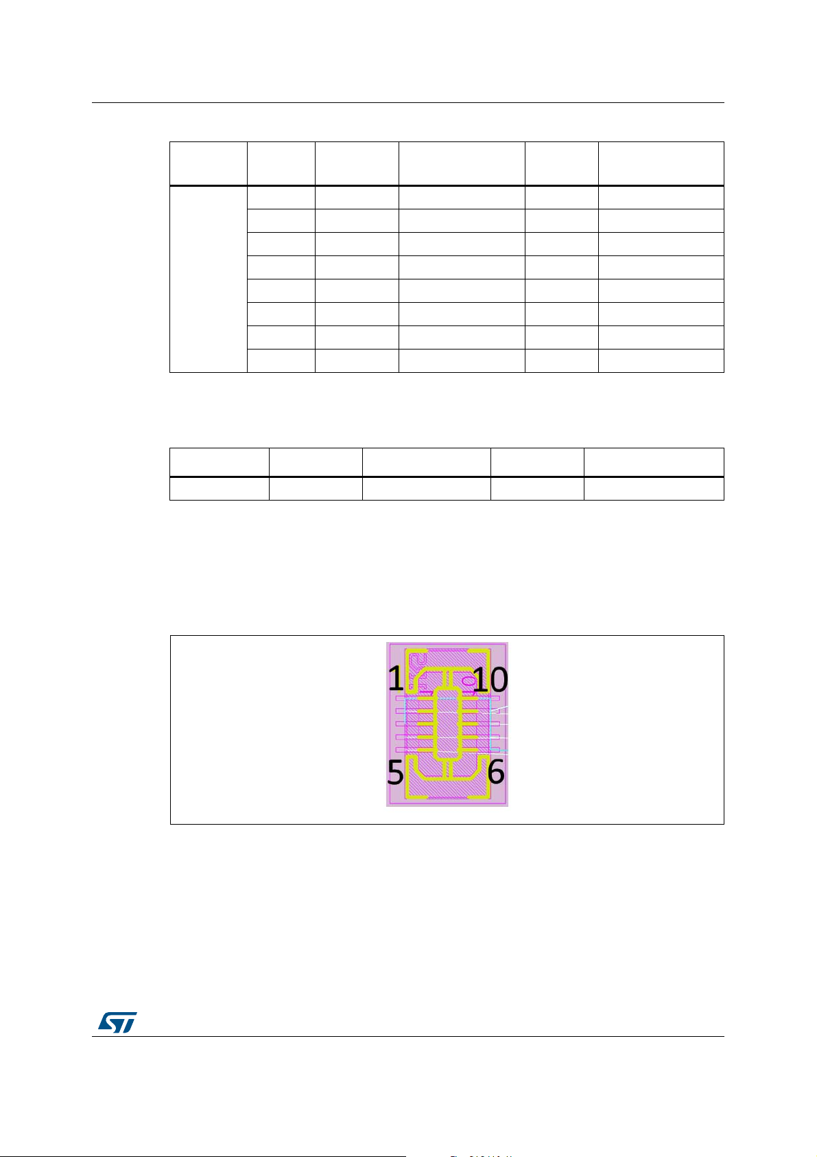
Example of connector reference (see Figure 21):
• Amphemol-FCI 20021311-00020T4LF
DocID029965 Rev 1 27/50
49
Connectors UM2135
Figure 21. Extension microphone connector (front view)
Table 13. Extension microphone connector
Connector Pin number Pin name Signal name STM32 pin Function
1 GND GND - Power
2V
CC_0
3.3 V - Ground
3 CLK_1 EXT_DFSDM2_CKOUT PD2 DFSDM2 CLOCK
4 CLK_0 EXT_DFSDM1_CKOUT PA8 DFSDM1 CLOCK
5 DATA_1 EXT_DFSDM2_DATIN1 PA7 DFSDM2 DATA1
6 DATA_0 EXT_DFSDM1_DATIN1 PD6 DFSDM1 DATA1
CN12
7 DATA_3 EXT_DFSDM2_DATIN7 PB7 DFSDM2 DATA7
8- - -
9- - - -
10 DETECTN DETECTN - -
11 - - - -
12 MEMS_LED MEMS_LED PE4 -
13 - - - -
14 - - - -
15 - - - -
16 - - - -
CN12
17 - - - -
18 - - - -
19 V
CC_1
3.3 V - Power
20 GND GND - Ground
8.10 Optional audio stereo speakers CN3 and CN4
The stereo audio outputs are available to support stereo speakers (CN3 for left channel and
CN4 for right channel).
28/50 DocID029965 Rev 1

UM2135 32F413HDISCOVERY I/O assignment
Appendix A 32F413HDISCOVERY I/O assignment
Table 14. 32F413HDISCOVERY I/O assignment
Pin No. Pin Name Signal or Label Feature / Comment
1 PE2 QSPI_BK1_IO2 QSPI
2 PE3 LED1_RED User LED
3 PE4 MEMS_LED Microphones MEMS Module
4 PE5 LCD_BL_CTRL LCD and CTP
5 PE6 ARD_D5 ARD_TIM9_CH2
6V
BAT
V
BAT
3.3V
7 PC13-ANTI_TAMP ARD_D7 ARD_IO
8 PC14-OSC32_IN OSC_32K_IN RTC CLK
9 PC15-OSC32_OUT OSC_32K_OUT RTC CLK
10 PF0 PSRAM_A0/LCD-RS_A0
Shared between LCD and
PSRAM
11 PF1 PSRAM_A1 PSRAM
12 PF2 PSRAM_A2 PSRAM
13 PF3 PSRAM_A3 PSRAM
14 PF4 PSRAM_A4 PSRAM
15 PF5 PSRAM_A5 PSRAM
16 V
17 V
SS_5
DD_5
V
V
SS_5
DD_5
GND
3.3 V
18 PF6 ARD_D0_URX ARD_UART7
19 PF7 ARD_D1_UTX ARD_UART7
20 PF8 QSPI_BK1_IO0 QSPI
21 PF9 QSPI_BK1_IO1 QSPI
22 PF10 ARD_D3_PWM ARD_TIM5_CH4
23 PH0-OSC_IN HSE_OSC_IN 8 MHz clock
24 PH1-OSC_OUT WIFI_RST Wi-Fi
25 NRST NRST_BUTTON RESET
26 PC0 ARD_A0 ARD_ADC1_IN10
27 PC1 CTP_INT Touch Panel INT
28 PC2 CODEC_I2Sext_SD I2S2
29 PC3 CODEC_I2S_SD I2S2
30 V
31 V
32 V
DD_12
SSA
REF+
V
DD_12
V
V
SSA
REF
3.3 V
GND
3.3 V
DocID029965 Rev 1 29/50
49

32F413HDISCOVERY I/O assignment UM2135
Table 14. 32F413HDISCOVERY I/O assignment (continued)
Pin No. Pin Name Signal or Label Feature / Comment
33 V
DDA
V
DDA
3.3 V
34 PA0-WKUP B_USER USER BUTTON
35 PA1 ARD_A1 ARD_ADC1_IN1
36 PA2 ARD_A2 ARD_ADC1_IN2
37 PA3 CODEC_I2S_MCLK AUDIO_I2S2
38 V
39 V
SS_4
DD_4
V
V
SS_4
DD_4
GND
3.3 V
40 PA4 ARD_D8_IO ARD
41 PA5 ARD_A3 ARD_ADC1_IN5
42 PA6 SD_CMD SD CARD
43 PA7 DFSDM2_DATIN1 ST-MEMS microphones
44 PC4 ARD_A5 ARD_ADC1_IN14
45 PC5 LED2_GREEN User LED
46 PB0 ARD_D6_PWM ARD_TIM3_CH3
47 PB1 ARD_A4 ARD_ADC1_IN9
48 PB2 QSPI_CLK QSPI
49 PF11 SD_Detect SD CARD_IT_11
50 PF12 PSRAM_A6 PSRAM
51 V
52 V
SS_6
DD_6
V
V
SS_6
DD_6
GND
3.3 V
53 PF13 PSRAM_A7 PSRAM
54 PF14 PSRAM_A8 PSRAM
55 PF15 PSRAM_A9 PSRAM
56 PG0 PSRAM_A10 PSRAM
57 PG1 PSRAM_A11 PSRAM
58 PE7 LCD-PSRAM_D4 LCD-PSRAM
59 PE8 LCD-PSRAM_D5 LCD-PSRAM
60 PE9 LCD-PSRAM_D6 LCD-PSRAM
61 V
62 V
SS_7
DD_7
V
V
SS_7
DD_7
GND
3.3 V
63 PE10 LCD-PSRAM_D7 LCD-PSRAM
64 PE11 LCD-PSRAM_D8 LCD-PSRAM
65 PE12 LCD-PSRAM_D9 LCD-PSRAM
66 PE13 LCD-PSRAM_D10 LCD-PSRAM
67 PE14 LCD-PSRAM_D11 LCD-PSRAM
30/50 DocID029965 Rev 1

UM2135 32F413HDISCOVERY I/O assignment
Table 14. 32F413HDISCOVERY I/O assignment (continued)
Pin No. Pin Name Signal or Label Feature / Comment
68 PE15 LCD-PSRAM_D12 LCD-PSRAM
69 PB10 ARD_D15_SCL ARD_I2C2
70 PB11 ARD_D14_SDA ARD_I2C2
71 V
72 V
CAP1_0
DD_1_0
V
CAP1_0
V
DD_1_0
73 PB12 ARD_D13_SCK SPI3 (ARD & WIFI)
74 PB13 LCD-CTP_RST LCD-CTP
75 PB14 LCD_TE LCD
76 PB15 WIFI_WKUP Wi-Fi
77 PD8 LCD-PSRAM_D13 LCD-PSRAM
78 PD9 LCD-PSRAM_D14 LCD-PSRAM
79 PD10 LCD-PSRAM_D15 LCD-PSRAM
80 PD11 PSRAM_A16 PSRAM
81 PD12 PSRAM_A17 PSRAM
82 PD13 QSPI_BK1_IO3 QSPI
PWR
3.3 V
83 V
84 V
SS_8
DD_8
V
V
SS_8
DD_8
GND
3.3 V
85 PD14 LCD-PSRAM_D0 LCD-PSRAM
86 PD15 LCD-PSRAM_D1 LCD-PSRAM
87 PG2 PSRAM_A12 PSRAM
88 PG3 PSRAM_A13 PSRAM
89 PG4 PSRAM_A14 PSRAM
90 PG5 PSRAM_A15 PSRAM
91 PG6 QSPI_BK1_NCS QSPI
92 PG7 USB_OTG_FS_OVRCR USB_INT_7
93 PG8 USB_OTG_FS_PWR_EN USB
94 V
95 V
DD_2_USB33
SS_9
V
SS_9
V
DD_2_USB33
GND
3.3 V
96 PC6 CTP_I2C_SCL CTP_I2CFMP1
97 PC7 CTP_I2C_SDA CTP_I2CFMP1
98 PC8 SD_D0 SD CARD
99 PC9 SD_D1 SD CARD
100 PA8 DFSDM1_CKOUT ST-MEMS microphones
101 PA9 USB_OTG_FS_VBUS USB
102 PA10 USB_OTG_FS_ID USB
DocID029965 Rev 1 31/50
49

32F413HDISCOVERY I/O assignment UM2135
Table 14. 32F413HDISCOVERY I/O assignment (continued)
Pin No. Pin Name Signal or Label Feature / Comment
103 PA11 USB_OTG_FS_DM USB
104 PA12 USB_OTG_FS_DP USB
105 PA13 DBG_SWDIO STLINK
106 V
107 V
108 V
CAP2_0
SS 2_0
DD_2_0
V
CAP2_0
V
SS 2_0
V
DD_2_0
109 PA14 DBG_SWCLK ST-LINK
110 PA15 ARD_D10_PWM_CS ARD_TIM2_CH1_SPI3
111 PC10 SD_D2 SD CARD
112 PC11 SD_D3 SD CARD
113 PC12 SD_CLK SD CARD
114 PD0 LCD-PSRAM_D2 LCD-PSRAM
115 PD1 LCD-PSRAM_D3 LCD-PSRAM
116 PD2 DFSDM2_CKOUT Microphones MEMS
117 PD3 CODEC_I2S_CK AUDIO_I2S2
PWR
GND
3.3 V
118 PD4 LCD-PSRAM_NOE LCD-PSRAM
119 PD5 LCD-PSRAM_NWE LCD-PSRAM
120 V
121 V
SS_10
DD_10
V
SS_10
V
DD_10
GND
3.3 V
122 PD6 DFSDM1_DATIN1 ST-MEMS microphones
123 PD7 PSRAM_NE1 PSRAM
124 PG9 UART_VCP_RX STLINK_UART6
125 PG10 LCD_NE3 LCD
126 PG11 WIFI_SPI_CSN WIFI_SPI_CS
127 PG12 WIFI_DRDY Wi-Fi
128 PG13 ARD_D2_IO ARD
129 PG14 UART_VCP_TX STLINK_UART6
130 VSS_11 V
131 VDD_11 V
SS_11
DD_11
GND
3.3 V
132 PG15 CODEC_INT AUDIO_INT15
133 PB3 DBG_SWO ST-LINK
134 PB4 ARD_D12_MISO SPI3 (ARD & WIFI)
135 PB5 ARD_D11_PWM_MOSI SPI3 (ARD & WIFI)
136 PB6 ARD_D4_INT ARD_INT_6
137 PB7 DFSDM2_DATIN7 ST-MEMS microphones
32/50 DocID029965 Rev 1

UM2135 32F413HDISCOVERY I/O assignment
Table 14. 32F413HDISCOVERY I/O assignment (continued)
Pin No. Pin Name Signal or Label Feature / Comment
138 BOOT0 BOOT0 BOOT
139 PB8 ARD_D9_PWM ARD_TIM4_CH3
140 PB9 CODEC_I2S_WS AUDIO_I2S2
141 PE0 PSRAM_NBL0 PSRAM
142 PE1 PSRAM_NBL1 PSRAM
143 PDR_ON PDR_ON PDR
144 V
DD_3
V
DD_3
3.3 V
DocID029965 Rev 1 33/50
49

Schematics UM2135
Appendix B Schematics
This section provides the design schematics for the 32F413HDISCOVERY Discovery kit:
• Overall schematics for the 32F413HDISCOVERY, see Figure 22
• 32F413HDISCOVERY MCU, see Figure 23
• PSRAM, see Figure 24
• Quad-SPI, see Figure 25
• Audio, see Figure 26
• LCD, see Figure 27
• USB OTG FS, see Figure 28
• Peripherals, see Figure 29
• Arduino Uno V3 connector, see Figure 30
• ST-LINK with support of SWD only, see Figure 31
• Power, see Figure 32
34/50 DocID029965 Rev 1
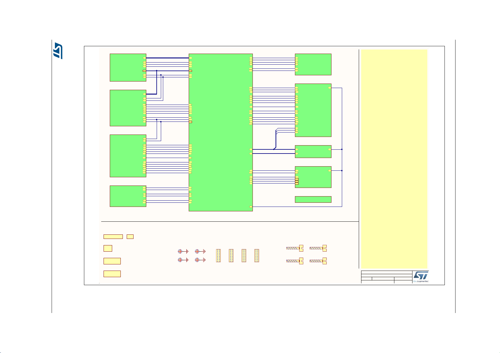
Figure 22. Top
111
MB1274-TOP
MB1274 D-01
12/19/2016
Title:
Size: Reference:
Date: Sheet: of
A3
Revision:
STM32F413H-DISCOProject:
PSRAM_A[0..17]
LCD-PSRAM_D[0..15]
NRST
QSPI_BK1_IO3
QSPI_BK1_IO2
QSPI_BK1_IO0
QSPI_BK1_IO1
QSPI_CLK
QSPI_BK1_NCS
USB_OTG_FS_OVRCR
USB_OTG_FS_PWR_EN
B_USER
STLK_MCO
CODEC_INT
LCD_TE
LCD_BL_CTRL
PSRAM_A[0..17]
LCD-PSRAM_D[0..15]
LCD-PSRAM_NWE
LCD-PSRAM_NOE
PSRAM_NE1
PSRAM_NBL0
PSRAM_NBL1
LCD_NE3
LCD-CTP_RST
CTP_INT
LED1_RED
LED2_GREEN
USB_OTG_FS_VBUS
USB_OTG_FS_ID
I2CFMP1_SDA
I2CFMP1_SCL
USB_OTG_FS_N
USB_OTG_FS_P
STLINK_JTMS_SWDIO
STLINK_JTCK_SWCLK
STLINK_JTDO-SWO
LCD-RS_A0
SD_D2
WIFI_SPI_CSN
DFSDM2_DATIN7
WIFI_DRDY
SD_D3
SD_CLK
DFSDM1_DATIN1
DFSDM2_DATIN1
DFSDM1_CKOUT
SD_Detect
SD_CMD
SD_D0
SD_D1
DFSDM2_CKOUT
CODEC_WS
CODEC_CK
CODEC_SD
CODEC_MCK
CODEC_ext_SD ARD_A[0..5]
ARD_D[0..15]
VCP_TX
VCP_RX
WIFI_WKUP
MEMS_LED
WIFI_RST
U_00_MCU
00_MCU.SchDoc
PSRAM_A[0..17]
LCD-PSRAM_D[0..15]
LCD-PSRAM_NWE
LCD-PSRAM_NOE
PSRAM_NE1
PSRAM_NBL0
PSRAM_NBL1
U_01_PSRAM
01_PSRAM.SchDoc
QSPI_BK1_IO0
QSPI_BK1_IO2
QSPI_BK1_IO1
QSPI_BK1_IO3
QSPI_CLK
QSPI_BK1_NCS
U_02_QSPI
02_QSPI.SchDoc
LCD_BL_CTRL
CTP_INT
LCD_TE
LCD-CTP_RST
LCD_NE3
LCD-PSRAM_D[0..15]
LCD-PSRAM_NWE
LCD-PSRAM_NOE
LCD-RS_A0
I2CFMP1_SDA
I2CFMP1_SCL
U_04_LCD
04_LCD.SchDoc
CODEC_INT
I2CFMP1_SCL
I2CFMP1_SDA
DFSDM1_DATIN1
DFSDM1_CKOUT
DFSDM2_CKOUT
DFSDM2_DATIN1
DFSDM2_DATIN7
CODEC_CK
CODEC_WS
CODEC_SD
CODEC_ext_SD
CODEC_MCK
MEMS_LED
U_03_Audio
03_Audio.SchDoc
USB_OTG_FS_VBUS
USB_OTG_FS_ID
USB_OTG_FS_PWR_EN
USB_OTG_FS_OVRCR
USB_OTG_FS_N
USB_OTG_FS_P
U_05_USB_OTG_FS
05_USB_OTG_FS.SchDoc
LED1_RED
LED2_GREEN
NRST
B_USER
SD_CLK
SD_CMD
SD_D0
SD_D1
SD_D2
SD_D3
SD_Detect
WIFI_SPI_CSN
WIFI_DRDY
WIFI_RST
WIFI_WKUP
ARD_D11
ARD_D12
ARD_D13
U_06_Peripherals
06_Peripherals.SchDoc
NRST
ARD_A[0..5]
ARD_D[0..15]
U_07_Arduino_ Connectors
07_Arduino_ Connectors.SchDoc
NRST
NRST
NRST
NRST
N
COMMENT to give more details about the function, or it is the MCU
port information.
REVISION D01
Add U21 for USB_VBUS ESD protection.
REVISION C01:
Released 22 - November- 2016
- USB ESD: U19 update (rotation).
REVISION B01:
Released 05 - October- 2016
- Update WIFI module with new reference
- Update IO assignment for PA0, PC0, PC1 and PC13.
- Update USB ESD protection.
- LD2: Correction of LD2, LD2 was mirrored on revA
- HW5: Update Capacitive touch Panel to rev B instead of revision A
REVISION A01
Released : 09 - June - 2016
- First version
PCB
HW1
STM32F413H-DISCO PCB 4L
BLISTER
HW2
STM32F413H-DISCO BLISTER
BLISTER CARD
HW3
STM32F413H-DISCO BLISTER CARD
HW PART
NRST
STLINK_JTDO-SWO
STLK_MCO
STLINK_JTMS_SWDIO
STLINK_JTCK_SWCLK
VCP_RX
VCP_TX
U_08_ST_LINK_V2-1
08_ST_LINK_V2-1.SCHDOC
U_09_Power
09_Power.SchDoc
H3 H1
H2 H4
HW8
Spacer 14mm
HW9
Spacer 14mm
HW10
Spacer 14mm
HW11
Spacer 14mm
HW7
Plastic Screw M3x6mm
HW6
Plastic Screw M3x6mm
HW13
Plastic Screw M3x6mm
HW12
Plastic Screw M3x6mm
ARD_D11
ARD_D12
ARD_D13
ARD_D[0..15]
mb1274 B-01
Serial Number
HW17
ES
HW18
UM2135 Schematics
ote: Text in BLUE placed on a wire is not the net name. It just a
DocID029965 Rev 1 35/50

36/50 DocID029965 Rev 1
211
MCU
MB1274 D-01
12/16/2016
Title:
Size: Reference:
Date: Sheet: of
A3
Revision:
STM32F413H-DISCOProject:
SD_D0
SD_D1
SD_D2
SD_D3
SD_CLK
LCD-PSRAM_D13
LCD-PSRAM_D14
LCD-PSRAM_D15
SD_CMD
LCD-PSRAM_D4
LCD-PSRAM_D5
LCD-PSRAM_D6
LCD-PSRAM_D7
LCD-PSRAM_D8
LCD-PSRAM_D9
LCD-PSRAM_D10
LCD-PSRAM_D11
LCD-PSRAM_D12
NRST
BOOT0
VDD_MCU
VREF+
VDD_MCU
Ceramic capacitor (Low ESR)
VDD_MCU
VDD_MCU VDD_MCU
3V3 3V3
VDD_USB33
QSPI_BK1_IO3
CODEC_WS
QSPI_BK1_IO2
QSPI_BK1_IO0
QSPI_BK1_IO1
SD_Detect
QSPI_CLK
CODEC_CKCODEC_SDCODEC_MCK
QSPI_BK1_NCS
USB_OTG_FS_OVRCR
USB_OTG_FS_PWR_EN
VCP_TX
VCP_RX
B_USER
STLK_MCO
One 100nF placed close to each VDD_x pin of MCU
CODEC_ext_SD
CODEC_INT
LCD_TE
LCD_BL_CTRL
Close to MCU
Close to MCU
PDR ON by default
VDD_MCU
INTERRUPTION SOURCES
EXT_IT_0: User Wake-Up Button connected toP A0-WKUP1
EXT_IT_1: CapacitiveTouch Panel: CTP_INT connected to PC1: (WKUP3)
EXT_IT_6: ARD_INT connectedto PB6
EXT_IT_7: USB Overcurrent: USB_OTG_FS_OVRCR connected to PG7:
EXT_IT_11: MicroSDdetection: uSD_Detect connected to PF11:
EXT_IT_12: WIFI DATA RDY connected to PG12
EXT_IT_14: LCD Tearing Effect:LCD_TE connected to PB14:
OSC32_IN
OSC32_OUT
PH0-OSC_IN
PH1-OSC_OUTPDR_ON
PSRAM_A[0..17]
LCD-PSRAM_D[0..15]
LCD-PSRAM_NWE
LCD-PSRAM_NOE
PSRAM_NE1
PSRAM_NBL0
PSRAM_NBL1
PSRAM_A[0..17]
LCD-PSRAM_D[0..15]
LCD-PSRAM_D0
LCD-PSRAM_D1
LCD-PSRAM_D2
LCD-PSRAM_D3
PSRAM_A0
PSRAM_A1
PSRAM_A2
PSRAM_A3
PSRAM_A4
PSRAM_A5
PSRAM_A6
PSRAM_A7
PSRAM_A8
PSRAM_A9
PSRAM_A10
PSRAM_A11
PSRAM_A12
PSRAM_A13
PSRAM_A14
PSRAM_A15
PSRAM_A16
PSRAM_A17
LCD_NE3
LCD-CTP_RST
I2C2_PULL-UP
ARD_D15
ARD_D14
3V3
DECOUPLING CAPACITORS
EXT_IT_1
CTP_INT
EXT_IT_7
EXT_IT_15
EXT_IT_11
MCU GPIO BANK D, E, F, G
STLK_MCO
MCU PWR
I2CFMP1_SDA
I2CFMP1_SCL
X3
NX3215SA-32.768K
R104
2K7
R102
2K7
R56
2K7
R57
2K7
C54
100nF
C53
100nF
C59
100nF
C61
100nF
C63
100nF
C65
100nF
C67
100nF
C66
100nF
C62
100nF
C60
100nF
C56
100nF
C55
4.7uF
I2CFMP1_SCL
I2CFMP1_SDA
FCM1608KF-601T03
L1
100uH
C49
1uF
C52
100nF
C68
100nF
C48
1uF
C70
1uF
C51
100nF
C69
2.2uF
C64
2.2uF
R51
56R
32.768KHz CLOCK
8MHz CLOCK
MCU GPIO BANK A, B, C, and SYSTEM
DFSDM2_CKOUT
3V3
Fitted: NO
R54
10K
VDDA
LED1_RED
LED2_GREEN
USB_OTG_FS_VBUS
USB_OTG_FS_ID
I2CFMP1_SDA
I2CFMP1_SCL
I2CFMP1 shared between
Audio Codec and touch screen
DFSDM1_DATIN1
DFSDM1_CKOUT
I2CFMP1_PULL-UP
USB_OTG_FS_N
USB_OTG_FS_P
STLINK_JTMS_SWDIO
STLINK_JTCK_SWCLK
STLINK_JTDO-SWO
LCD-RS_A0
R55
10K
R52
10K
Fitted: NO
R53
10K
R48 0R
R47 0R
Fitted: NO
R45 0R
Fitted: NO
R44 0R
Fitted: NO
C44 8.2pF
Fitted: NO
C43 8.2pF
PH0-OSC_IN
23
PH1-OSC_OUT
24
NRST
25
PA0-WKUP1
34
PA1
35
PA2
36
PA3
37
PA4
40
PA5
41
PA6
42
PA7
43
PB0
46
PB1
47
PB2-BOOT1
48
PB10
69
PB11
70
PB12
73
PB13
74
PB14
75
PB15
76
PA8
100
PA9
101
PA10
102
PA11
103
PA12
104
PA13
105
PA14
109
PA15
110
PB3
133
PB4
134
PB5
135
PB6
136
PB7
137
BOOT0
138
PB8
139
PB9
140
PC13-ANTI_TAMP
7
PC14-OSC32_IN
8
PC15-OSC32_OUT
9
PC0
26
PC1
27
PC2
28
PC3
29
PC4
44
PC5
45
PC6
96
PC7
97
PC8
98
PC9
99
PC10
111
PC11
112
PC12
113
PDR_ON
143
U13A
STM32F413H
PE2
1
PE3
2
PE4
3
PE5
4
PE6
5
PE7
58
PE8
59
PE9
60
PE10
63
PE11
64
PE12
65
PE13
66
PE14
67
PE15
68
PD8
77
PD9
78
PD10
79
PD11
80
PD12
81
PD13
82
PD14
85
PD15
86
PD0
114
PD1
115
PD2
116
PD3
117
PD4
118
PD5
119
PD6
122
PD7
123
PE0
141
PE1
142
PF2
12
PF3
13
PF4
14
PF5
15
PF6
18
PF7
19
PF8
20
PF9
21
PF10
22
PF11
49
PF12
50
PF13
53
PF14
54
PF15
55
PF0
10
PF1
11
PG2
87
PG3
88
PG4
89
PG5
90
PG6
91
PG7
92
PG8
93
PG9
124
PG10
125
PG11
126
PG12
127
PG13
128
PG14
129
PG15
132
PG0
56
PG1
57
U13B
STM32F413H
Fitted: NO
12
X2
NX3225GD-8.00M
VBAT
6
VSS_5
16
VDD_5
17
VSSA_VREF-
31
VDD_12
30
VREF+
32
VDDA
33
VSS_4
38
VDD_4
39
VCAP1
71
VDD_1
72
VSS_2
107
VDD_2
108
VDD_3
144
VDD_10
121
VDD_USB
95
VDD_6
52
VDD_7
62
VDD_8
84
VDD_11
131
VSS_10
120
VSS_9
94
VSS_6
51
VSS_7
61
VSS_8
83
VSS_11
130
VCAP2
106
U13C
STM32F413H
R58
0R_0603
VDD_MCU
R43
0R_0603
C50
100nF
R46
0R
R50 0R
Should be place closed to the MCU
C47 5.1pF
C46 5.1pF
WIFI_WKUP
DFSDM2_DATIN1
DFSDM2_DATIN7
WIFI_DRDY
WIFI_SPI_CSN
WIFI_RST
ARD_A[0..5]
ARD_A[0..5]
ARD_A0
ARD_A1
ARD_A2
ARD_A3
ARD_A4
ARD_A5
ARD_D[0..15]
ARD_D[0..15]
ARD_D6
ARD_D12
ARD_D11
ARD_D4
ARD_D9
ARD_D15
ARD_D14
ARD_D13
ARD_D7
ARD_D8
ARD_D2
ARD_D0
ARD_D1
ARD_D3
ARD_D5
ARD_D10
EXT_IT_0 / WKUP1
MEMS_LED
NRST
R49 0R
Figure 23. MCU
Schematics UM2135
EXT_IT_15: Audio CODEC interruption: CODEC_INT connected toP G15:

311
PSRAM
MB1274 D-01
12/16/2016
Title:
Size: Reference:
Date: Sheet: of
A4
Revision:
STM32F413H-DISCOProject:
LCD-PSRAM_D[0..15]
PSRAM_A[0..17]
PSRAM
3V3
3V3
Place close to PSRAM
PSRAM_A0
PSRAM_A1
PSRAM_A2
PSRAM_A3
PSRAM_A4
PSRAM_A5
PSRAM_A6
PSRAM_A7
PSRAM_A8
PSRAM_A9
PSRAM_A10
PSRAM_A11
PSRAM_A12
PSRAM_A13
PSRAM_A14
PSRAM_A15
PSRAM_A16
PSRAM_A17
PSRAM_A[0..17]
LCD-PSRAM_D[0..15]
LCD-PSRAM_NWE
LCD-PSRAM_NOE
PSRAM_NE1
PSRAM_NBL0
PSRAM_NBL1
R60
10K
R59 0R
R61 0R
C72
100nF
C71
100nF
LCD-PSRAM_D0
LCD-PSRAM_D1
LCD-PSRAM_D2
LCD-PSRAM_D3
LCD-PSRAM_D4
LCD-PSRAM_D5
LCD-PSRAM_D6
LCD-PSRAM_D7
LCD-PSRAM_D8
LCD-PSRAM_D9
LCD-PSRAM_D10
LCD-PSRAM_D11
LCD-PSRAM_D12
LCD-PSRAM_D13
LCD-PSRAM_D14
LCD-PSRAM_D15
i
PSRAM_D
Matched Net Lengths [Tolerance = 5mm]
Impedance Constraint [Min = 40.00 Max = 60.00 ]
i
PSRAM_A
Matched Net Lengths [Tolerance = 5mm]
Impedance Constraint [Min = 40.00 Max = 60.00 ]
i
PSRAM_A
i
PSRAM_A
i
PSRAM_A
i
PSRAM_A
i
PSRAM_A
PSRAM Data, NWE & NOE shared with LCD
PD7
PD5
PD4
PE0
PE1
A4
B4
A3
B3
A2
A5
A1
A4
A0
A3
CS1
B5
I/O0
B6
I/O1
C5
I/O2
C6
I/O3
D5
VDD
D6
GND
D1
I/O4
E5
I/O5
F5
I/O6
F6
I/O7
G6
WE
G5
A16
E4
A15
F4
A14
F3
A13
G4
A12
G3
A11
H5
A10
H4
A9
H3
A8
H2
I/O8
B1
I/O9
C1
I/O10
C2
I/O11
D2
VDD
E1
I/O12
E2
I/O13
F2
I/O14
F1
I/O15
G1
LB
A1
UB
B2
OE
A2
A7
D4
A6
C4
A5
C3
A17
D3
A18
H1
GND
E6
NC
G2
CS2
A6
NC
H6
NC
E3
U14
IS66WV51216EBLL-55BLI
R62
10K
Figure 24. PSRAM
UM2135 Schematics
DocID029965 Rev 1 37/50

411
QSPI
MB1274 D-01
12/16/2016
Title:
Size: Reference:
Date: Sheet: of
A4
Revision:
STM32F413H-DISCOProject:
QSPI_BK1_IO0
QSPI_BK1_IO2
QSPI_BK1_IO1
QSPI_BK1_IO3
3V3
QSPI_CLK
QSPI_BK1_NCS
Exposed central pad should not be connected to any voltage on PCB
3V3
3V3
Optional PU and PD to set PB2 when use in BOOT1 alternate function
R31
10K
C28
100nF
QSPI
i
QSPI
Matched Net Lengths [Tolerance = 5mm]
i
QSPI
i
QSPI
i
QSPI
i
QSPI
i
QSPI
DQ3/HOLD#
7
VCC
8
S#
1
DQ1
2
C
6
DQ0
5
VSS
4
DQ2/Vpp/W#
3
Q
3
/
O
#
V
CCS#
DQ1
C
Q
0
V
SS
Q
2
/
V
p
p
/
W
#
U9
N25Q128A13EF840F
Fitted: NO
R21 10K
Fitted: NO
R20 10K
PG6
PB2
PF8
PF9
PE2
PD13
QSPI_CLK
TP4
QSPI_BK1_IO0
TP3
QSPI_BK1_IO1
TP6
38/50 DocID029965 Rev 1
Figure 25. Quad-SPI
D
D
D
Schematics UM2135

Figure 26. Audio
511
Audio
MB1274 D-01
12/16/2016
Title:
Size: Reference:
Date: Sheet: of
A3
Revision:
STM32F413H-DISCOProject:
CODEC_CK
ADCDAT1
F2
ADCLRCLK1/GPIO1
G3
AGND
D6
CPVDD
G9
CPVOUTN
H7
CPVOUTP
G7
CS/ADDR
G2
DACDAT1
E4
CPGND
H9
DCVDD
F1
DBVDD
D2
DGND
E2
CPCB
H8
AVDD1
D9
BCLK1
G1
CIFMODE
A4
CPCA
G8
DMICCLK
C6
AGND
E7
AGND
E8
AVDD2
D8
GPIO2/MCLK2
E1
GPIO3/BCLK2
H2
GPIO4/LRCLK2
F4
GPIO5/DACDAT2
H3
GPIO6/ADCLRCLK2
G4
GPIO7/ADCDAT2
E5
GPIO8/DACDAT3
H4
GPIO9/ADCDAT3
F5
GPIO10/LRCLK3
H5
GPIO11/BCLK3
F6
HP2GND
F7
HPOUT1FB
G5
HPOUT1L
H6
HPOUT1R
G6
HPOUT2N
F9
HPOUT2P
F8
IN1LN
D7
IN1LP
C8
IN1RN
B7
IN1RP
C7
IN2LN/DMICDAT1
B9
IN2LP/VRXN
B8
IN2RN/DMICDAT2
A9
IN2RP/VRXP
A8
LDO1ENA
D4
LDO1VDD
E9
LDO2ENA
D5
LDO2VDD
D1
LINEOUT1N
C5
LINEOUT1P
B5
LINEOUT2N
C4
LINEOUT2P
B4
LINEOUTFB
A6
LRCLK1
E3
MCLK1
D3
MICBIAS1
A7
MICBIAS2
B6
REFGND
A5
SCLK
H1
SDA
F3
SPKGND1
A1
SPKGND2
C1
SPKMODE
A3
SPKOUTLN
B1
SPKOUTLP
A2
SPKOUTRN
C3
SPKOUTRP
B3
SPKVDD1
B2
SPKVDD2
C2
VMIDC
C9
VREFC
E6
U11
WM8994ECS/R
1V8
3V3
CODEC_WS
CODEC_SD
CODEC_INT
CODEC_MCK
3V3
3V3
3V3
Operating range: 1.62<VDD<3.6V
GND
21mm distance between a pair of microphones
CODEC_ext_SD
DFSDM1_DATIN1
1V8
3V3
DMIC1_DFSDM1_CKOUT
DMIC1_DFSDM1_DATIN1
DMIC1_DFSDM1_DATIN1
DFSDM1_CKOUT
DMIC1_DFSDM1_CKOUT
SPEAKER OUT RIGHT
CODEC PWR 1V8 / 150mA
CODEC WOLFSON
MEMS
R23 0R_0603
R28 0R_0603
R33 0R_0603
R22 0R_0603
R29 0R_0603
R26 0R_0603
R39 2K2
R12 0R_0603
C45
10nF
WM8994 I2C Address : 0011 0100
3V3
21mm distance between a pair of microphones
51
2
GND
3
4
BYPASS
INH
Vin Vout
U12 LD3985M18R
C35
100nF
C24
4.7uF
C25
100nF
C82
100nF
C26
100nF
I2CFMP1_SDA
I2CFMP1_SCL
Fitted: NO
R25 0R_0603
HP_OUT_L
HP_OUT_R
MIC_IN
C38 4.7uF
C37
4.7uF
C39
4.7uF
C32
4.7uF
C22 1uF
C23
1uF
C41 1uF
C34 1uF
C29
100nF
C31
100nF
C1 100nF
C2 100nF
C80 100nF
C79 100nF
C36 2.2uF
C40 2.2uF
C33 2.2uF
R30 10K
R1 10K
R80 10K
R32
20R
R35
20R
Fitted: NO
GND
3
LR
2
CLK
4
VDD
5
DOUT
1
U1
MP23DB01MMTR
Fitted: NO
GND
3
LR
2
CLK
4
VDD
5
DOUT
1
U2
MP23DB01MMTR
GND
5
LR
2
CLK
3
VDD
1
DOUT
4
U17
MP34DT01TR-M
GND
5
LR
2
CLK
3
VDD
1
DOUT
4
U16
MP34DT01TR-M
PC6
PC7
PG15
PA3
PD3
PB9
PC3
PC2
PA8
PD6
SPEAKER OUT LEFT
Extension microphones module
DMIC1_DFSDM1_CKOUT
DMIC1_DFSDM1_DATIN1
Microphone switch
EXT_DFSDM1_CKOUT
EXT_DFSDM1_DATIN1
EXT_DFSDM1_CKOUT
EXT_DFSDM1_DATIN1
DFSDM2_CKOUT
PD2
DFSDM2_DATIN1
PA7
DFSDM2_DATIN7
DETECTn
3V3
3V3
PB7
COM1
14
COM2
2
IN1-2
16
COM3
6
COM4
10
NC1
15
NO1
13
NC2
3
NO2
1
NC3
7
NO3
5
NC4
11
NO4
9
VCC12GND
4
IN3-4
8
U8
TS3A44159PWR
R13
10K
C16
1uF
3V3
NC = Normally Closed / NO Normally Open
IN = L => COM TO NC / NC TO COM (NO OFF)
DETECTn
Fitted: NO
1
2
CN3
Fitted: NO
1
2
CN4
20021311-00020T4LF
1
3
5
7
9
11
13
15
17
19
2
4
6
8
10
12
14
16
18
20
CN12
Receptacle 10X2 TH VT 1.27mm
CODEC_CK
TP14
CODEC_WS
TP11
CODEC_SD
TP7
CODEC_INT
TP8
CODEC_ext_SD
TP5
TP16TP1
TP10
DFSDM1_CKOUT
TP2
DFSDM1_DATIN1
TP13
DFSDM2_CKOUT
TP15
DFSDM2_DATIN1
TP12
Receptacle connector pin 1 connected to
header connector pin 2
DFSDM2_DATIN7
TP9
DMIC2_DFSDM2_CKOUT
DMIC2_DFSDM2_CKOUT
DMIC2_DFSDM2_DATIN1
DMIC2_DFSDM2_DATIN1
DMIC2_DFSDM2_CKOUT
DMIC2_DFSDM2_DATIN1
EXT_DFSDM2_CKOUT
EXT_DFSDM2_DATIN1
EXT_DFSDM2_CKOUT
EXT_DFSDM2_DATIN1
MEMS_LED
PE4
.
.
..
.
HW16
mb1299_A02
2
6
4
3
PJ3028B-3_4P
CN5
UM2135 Schematics
DocID029965 Rev 1 39/50
IN = H =>COM TO NO / NO TO COM (NC OFF)

40/50 DocID029965 Rev 1
611
LCD
MB1274 D-01
12/16/2016
Title:
Size: Reference:
Date: Sheet: of
A3
Revision:
STM32F413H-DISCOProject:
LCD_BL_CTRL
BLGND
BLGNDBLGND
BLGND
VL
Backlight driver & PFC connector for LCD panel
BLGND
5V
LCD-PSRAM_D8
LCD-PSRAM_D7 LCD-PSRAM_D6
LCD-PSRAM_D5 LCD-PSRAM_D4
LCD-PSRAM_D3
LCD-PSRAM_D1 LCD-PSRAM_D0
LCD-CTP_RST
LEDA
LEDK
LCD_NE3
LCD-PSRAM_NWELCD-PSRAM_NOE
3V3 3V3
Common mode supply filter
LEDA
LEDK
Backlight control: ON/OFF or dimmer by low frequency (1 to 10kHz typ.)
current regulated at 15mA
Layout: parts close to STLD40D and grouped in same area with BLGND as local ground plane
BLGND
3V3
3V3
I2C max clock: 400kHz
CTP_INT
GND1FMARK
2
DB153DB14
4
DB135DB12
6
DB117DB10
8
DB99DB8
10
DB711DB6
12
DB513DB4
14
DB315DB2
16
DB117DB0
18
/RD19/WR
20
RS
21
/CS
22
RESET23IM
24
IOVCC25VCI
26
GND27LEDA
28
LEDK
29
CN16
FH26-29S-0.3SHW
LCD-PSRAM_D9
LCD-PSRAM_D10LCD-PSRAM_D11
LCD-PSRAM_D12LCD-PSRAM_D13
LCD-PSRAM_D14LCD-PSRAM_D15
Top side: layout of CN16
1
29
LCD FRIDA FRD154BP2901
FPC
CN16
HW4
FRIDA LCD FRD154BP2902
HW5
CTP LS015GF614A
LCD_TE
LCD_TE
LCD-CTP_RST
LCD_NE3
3V3
Capacitive Touch Panel
240x240 pixels TFT LCD
pixel (0,0) *
X
Y
*: standard orientation. Rotations by 90, 180 , 270 degrees possible by registers.
3V3
3V3
SB41 open and SB42 closed = IM high: LCD in 16bits mode
SB41 closed and SB42 opened = IM low : LCD in 8bits mode
VDD_MCU operating voltage range: 3V0 to 3V6
LCD-PSRAM_D0 LCD-PSRAM_D1
LCD-PSRAM_D2
LCD-PSRAM_D3
LCD-PSRAM_D4 LCD-PSRAM_D5
LCD-PSRAM_D6 LCD-PSRAM_D7
LCD-PSRAM_D9
LCD-PSRAM_D10 LCD-PSRAM_D11
LCD-PSRAM_D12
LCD-PSRAM_D8
LCD-PSRAM_D13
LCD-PSRAM_D14 LCD-PSRAM_D15
LCD_TE LCD-CTP_RST
LCD-RS_A0
LCD-PSRAM_NWE
LCD-PSRAM_NOELCD_NE3
LCD_BL_CTRL
GND
3V3
LCD signals access (2mm pitch)
LCD-PSRAM_D[0..15]
LCD-PSRAM_NWE
LCD-PSRAM_D[0..15]
LCD-PSRAM_D2
LCD-RS_A0
PWM using TIM9_CH1
LCD RSTand CTP RST share the same PIO for RST. Active LOW
FRIDA LCD
LCD Backlight
LCD-PSRAM_NOE
Solder: NO
SB23
Solder: YES
SB22
R105
100K
R103
100K
Fitted: NO
R88
100K
C81
100nF
FCM1608KF-601T03
Fitted: NO
L8
100uH
FCM1608KF-601T03
L6
100uH
FCM1608KF-601T03
L5
100uH
C87
100nF
FCM1608KF-601T03
L7
100uH
C89
100nF
C85
4.7uF
C86
10nF
L4
4.7uH 1A 180R
FCM1608KF-601T03
L2
100uH
R98
100K
D5
STPS1L40M
Vi
1
Rset
2
GND3FB
4
NC
5
Vo
6
EN
7
SW
8
PGND
9
U18
STLD40DPUR
R100
100K
R101
10R
C84
4.7uF
C83
10nF
FCM1608KF-601T03
L3
100uH
BLGND
LCD-RS_A0
3V3
LCD-CTP_RST
LCD_BL_CTRL
I2CFMP1_SDA
I2CFMP1_SCL
PB14
Fitted: NO
R99
100K
C88
10uF
PD4
PF0
PB13
PD5
PG10
PC1
PC6
PC7
PE5
Fitted: NO
1
3
5
7
9
11
13
15
17
19
2
4
6
8
10
12
14
16
18
20
21
23
25
22
24
26
CN15
TMMH-113-01-F-DV
Solder: YES
SB14
Solder: NO
SB13
3V3
To support CTP rev A
- CN4 PIN8 should be connected to GND
to support CTP rev B
- CN4 PIN8 shoud be conencted to IOVCC
GND
10
VDD
9
GND
8
RESET
7
GND
6
GND
1
INT
2
GND
3
SDA
4
SCL
5
CN10
DF37NB-10DS-0.4V (5x)
Figure 27. LCD
Schematics UM2135

711
USB_OTG_FS
MB1274 D-01
12/16/2016
Title:
Size: Reference:
Date: Sheet: of
A4
Revision:
STM32F413H-DISCOProject:
5V
3V3
USB_OTG_FS_VBUS
5V_USB_FS
USB_OTG_FS_N
USB_OTG_FS_P
USB_OTG_FS_ID
USB_OTG_FS_PWR_EN
3V3
USB Full Speed operating range voltage: 3.0V<VDDUSB<3.6V
GND
2
IN
5
EN
4
OUT
1
FAULT
3
U15
STMPS2141STR
Open Drain
R64
47K
R66
47K
C76
4.7uF
LD8
LED, Red, 0603
R63
0R
VBUS
1
DM
2
DP
3
ID
4
GND
5
Shield
6
USB_Micro-AB receptacle
Shield
7
Shield
8
Shield
9
EXP
10
CN17
475900001
3
1
2
T3
9013-SOT23
LD7
LED, Green, 0603
R107
330R
R69
47K
R70
100K
R67
0R_0603
VBUS OK LED
USB_OTG_FS
3V3
USB_OTG_FS_OVRCR
EXT_IT_7
R65
0R
3V3
VBUS OVRCR LED
VBUS_OVRCR
R108
1K
ESD PROTECTION SHOULD BE CLOSE TO THE CONNECTOR
PG7
PG8
PA9
PA11
PA12
PA10
12
U20
ESDALC6V1-1U2
IO2
3
GND
2
IO11IO_1
6
VBUS
5
IO_2
4
U19
USBLC6-2P6
12
U21
ESDA7P60-1U1M
USB_N
USB_P
Figure 28. USB OTG FS
UM2135 Schematics
DocID029965 Rev 1 41/50

42/50 DocID029965 Rev 1
811
Peripherals
MB1274 D-01
12/16/2016
Title:
Size: Reference:
Date: Sheet: of
A4
Revision:
STM32F413H-DISCOProject:
MICRO SD CARD
SD_CLK
SD_CMD
SD_D0
SD_D1
SD_D2
SD_D3
SD_Detect
LED1_RED
LED2_GREEN
NRST
The 2 LEDs are to p side
3V33V3
3V3
USER LED
RESET BUTTONUSER WAKE-UP Button
B_USER
3V3
Solder: YES
SB7
Solder: YES
SB6
C57
100nF
C58
100nF
R109
100K
R79
0R_0603
R81
47K
R82
47K
R83
47K
R84
47K
R85
47K
1
2
3
4
5
6
7
8
SW2
9
SW1
10
CN1
PJS008-2003-1
LD3
LED, Green, 0603
LD4
LED, Red, 0603
R94
1K
PC10
PC11
PA6
PC12
PC8
PC9
PF11
PA0
PE3
PC5
C90
10pF
C78
10pF
R106
1K
R73
1K
100nF should be place close to the MCU
10pF and 1K should be place close to the button
100nF should be place clos e to the MCU
10pF and 1K should be place clos e to the button
WIFI MODULE
R93
330R
PERIPHERALS
PG12
PG11
WIFI_RST
PB15
R74
10K
R71
10K
3V3
R75
10K
Fitted: NO
R78 10K
Fitted: NO
R77 10K
Fitted: NO
R72
10K
TDO
7
GND
1
VDD
2
TDI
6
TCK
5
GND
3
T
D
O
N
TDI
T
CK
N
TMS
4
TRSTN
8
GPIO0
23
CFG1
29
CFG0
28
GND
35
GPIO4
27
GPIO3
26
GPIO2
25
GPIO1
24
ADC1/SSN
12
ADC2/SCK
11
ADC3/MISO
10
ADC4/MOSI
9
ADC0/DATARDY
13
GND
17
WKUP
16
VBAT
15
VDD
14
DP
18
RX
21
GND
20
DM
19
TX
22
BOOT0
33
RES
32
RES
31
RES
30
RSTN
34
GND40GND38GND37GND36GND
39
GND43GND42GND41GND
44
M1
ISM43362-M3G-L44-E-SPI-Cxx
TP21 TRSTN
TP18 TDO
TP17 TDI
TP19 TCK
TP20 TMS
C77 1 00nFC75 100nF
C74 2.2u FC73 2.2uF
3V3
3V3
3V3
Fitted: NO
R76
10K
Solder: NO
SB11
Solder: NO
SB12
WIFI_SPI_CSN
WIFI_DRDY
R68
47K
Solder: YESSB8
Solder: YES
SB9
PG11 and PG12 can be use as
UART for debug purpose.
WIFI_WKUP
PH1
SPI3_MOSIPB5
PB4
PB12 SPI3_SCK
SPI3_MISO
ARD_D12
ARD_D11
ARD_D13
UART/SPI interface selection
UART: CFG0 = CFG1 = 1 (PU)
SPI: CFG0 = 1 (PU) / CFG1 = 0 (PD)
13
4 2
B2
BLACK_CMS_BUTTON
13
4 2
B1
BLUE_CMS_BUTTON
Solder: NOSB10
NRST
NRST
TP22
WIFI_BOOT0
Figure 29. Peripherals
Schematics UM2135
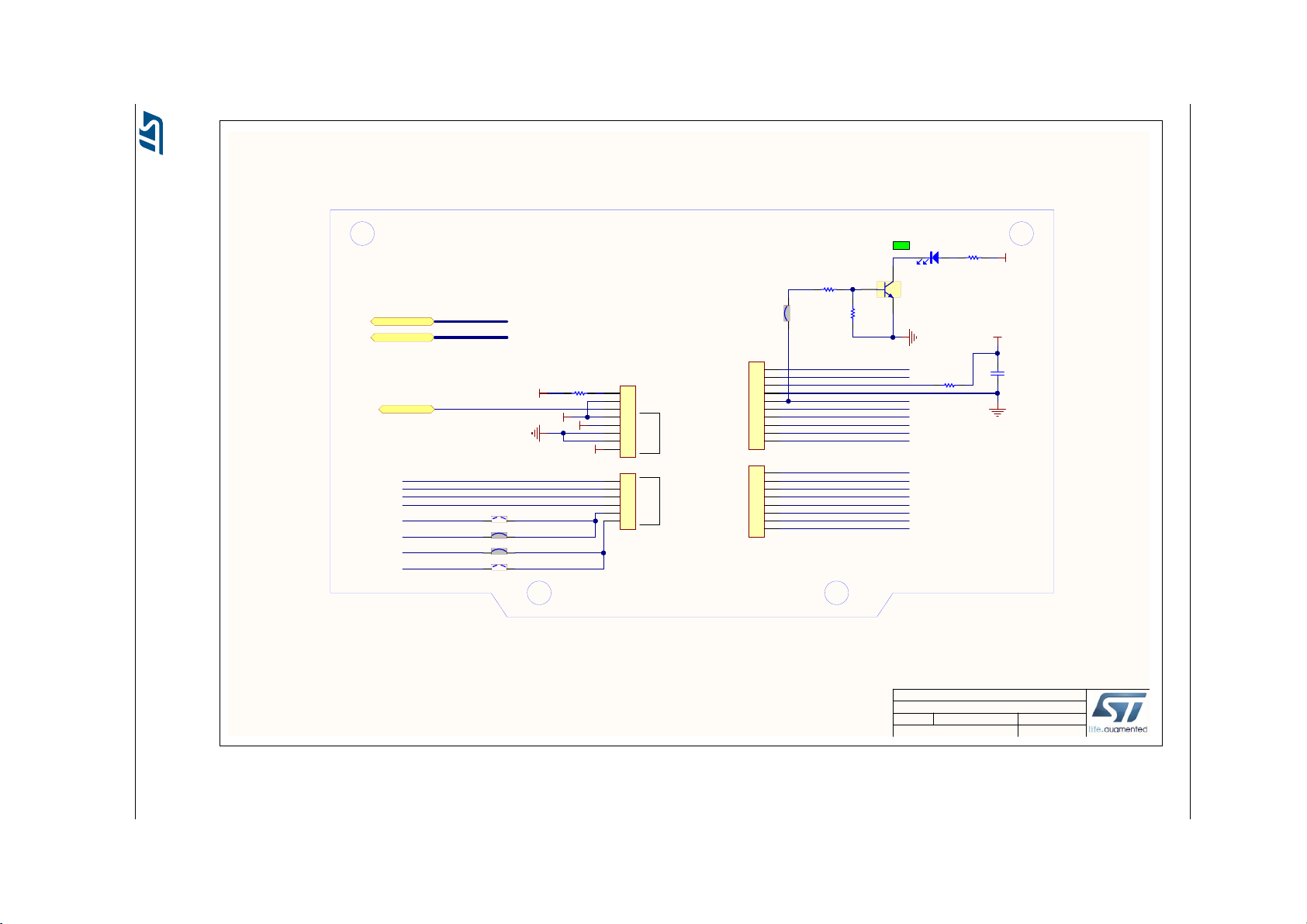
911
Arduino Uno connector
MB1274 D-01
12/16/2016
Title:
Size: Reference:
Date: Sheet: of
A4
Revision:
STM32F413H-DISCOProject:
ARDUINO UNO connector
A0
A1
A2
A3
A4
A5
RX/D0
TX/D1
D2
D4
PWM/D3
PWM/D5
PWM/D6
D7
D8
PWM/D9
PWM/CS/D10
SDA/D14
SCL/D15
VIN
NRST
SCK/D13
MISO/D12
PWM/MOSI/D11
AVDD
GND
VREF+
ADC1_IN5
ADC1_IN2
ADC1_IN1
ADC1_IN10
USART7_RX
USART7_TX
TIM5_CH4
TIM9_CH2
TIM4_CH3
TIM2_CH1, SPI3_NSS
TIM3_CH2, SPI3_MOSI
IOREF
NRST
3V3
5V
GND
GND
VIN
POWERAIN
TIM3_CH3
R96
510R
Solder: YES
SB5
3V3
5V
SDA/D14
SCL/D15
ADC1_IN9
ADC1_IN14
1
2
3
4
5
6
CN9
BL 1-6 G
1
2
3
4
5
6
7
8
CN7
BL 1-8 G
1
2
3
4
5
6
7
8
9
10
CN6
BL 1-10 G
1
2
3
4
5
6
7
8
CN8
BL 1-8 G
WARNING voltage applied to VIN <11.5V
EXT_IT_6
Fitted: NO
C42
100nF
Solder: YES
SB19
Solder: YES
SB21
Solder: NO
SB24
Solder: NO
SB20ARD_D14
ARD_D15
R40 0R
5V_ARD
NRST
PC0
PA1
PA2
PA5
PB1
PC4
PB10
PB11
PF6
PF7
PG13
PF10
PB6
PE6
PB0
PC13
PA4
PB8
PA15
PB5
PB4
PB12
ARD_D15
ARD_D14
IO
IO
IO
R95
1K
ARD_A[0..5]
ARD_A[0..5]
ARD_A0
ARD_A1
ARD_A2
ARD_A3
ARD_A4
ARD_A5
ARD_D[0..15]
ARD_D[0..15]
ARD_D0
ARD_D1
ARD_D2
ARD_D3
ARD_D4
ARD_D5
ARD_D6
ARD_D7
ARD_D8
ARD_D9
ARD_D10
ARD_D11
ARD_D12
ARD_D13SPI3_SCK
SPI3_MISO
I2C_SCL
I2C_SDA
(DAC1_OUT available)
(DAC2_OUT available)
3V3
3
1
2
T2
9013-SOT23
LD5
LED, Green, 0603
R42 47K
R41
100K
DocID029965 Rev 1 43/50
Figure 30. Arduino Uno V3 connector
UM2135 Schematics
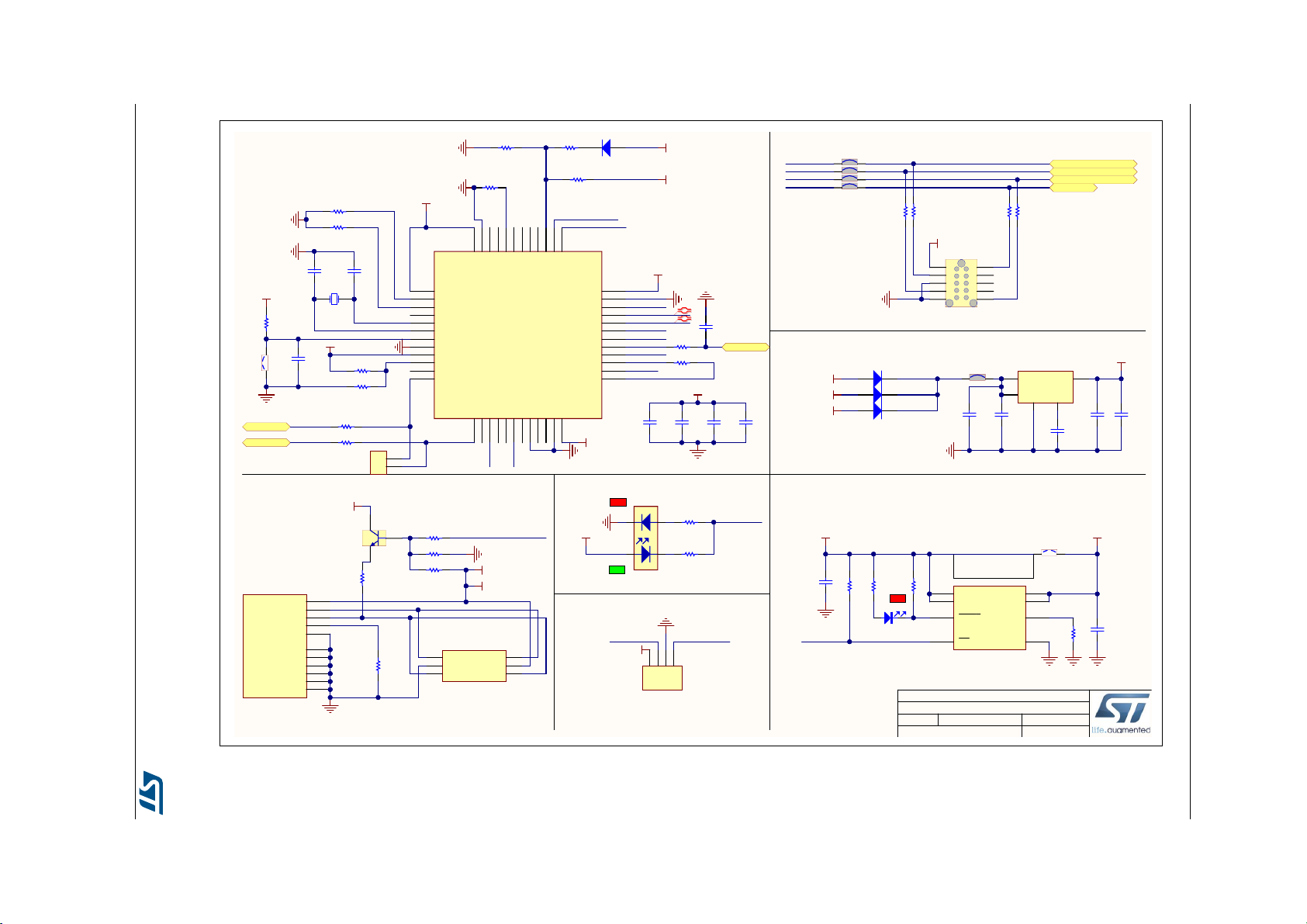
44/50 DocID029965 Rev 1
10 11
ST-LINK/V2-1 with support of SWD only
MB1274 D-01
12/16/2016
Title:
Size: Reference:
Date: Sheet: of
A4
Revision:
STM32F413H-DISCOProject:
STM_RST
T_JTCK
T_JTCK
T_JTMS
STM_JTMS
STM_JTCK
OSC_IN
OSC_OUT
T_NRST
AIN_1
3V3_ST_LINK
3V3_ST_LINK
USB_STLK_N
USB_STLK_P
ST-LINK USB CONNECTOR STLINK_LED
ST-LINK POWER 3V3 / 150mA
3V3_ST_LINK
Board Ident: PC13=0
T_JTCK
T_JTMS
SWD INTERFACE
3V3_ST_LINK
Fitted: NO
123
4
CN14 Header 4 pins
STM_JTMSSTM_JTCK
SWCLK SWDIO
3V3_ST_LINK
T_SWDIO_IN
T_SWO
LED_STLINK
LED_STLINK
3V3_ST_LINK
Red
_Green
21
34
LD2
LD_BICOLOR_CMS
NRST
T_NRST
51
2
GND
3
4
BYPASS
INH
Vin Vout
U7 LD3985M33R
VCP_RX
VCP_TX
STLINK_TX
STLINK_RX
3V3_ST_LINK
USB_RENUMn
PWR_EXT
PWR_ENn
3
1
2
T1
9013-SOT23
3V3_ST_LINK
USB_RENUMn
PWR_ENn
3V3_ST_LINK
3V3_ST_LINK
3V3_ST_LINK
VBAT
1
PA7
17
PC13
2
PA12
33
PC14
3
PB0
18
PC15
4
JTMS/SWDIO
34
OSCIN
5
PB1
19
OSCOUT
6
VSS_2
35
NRST
7
PB2/BOOT1
20
VSSA
8
VDD_2
36
VDDA
9
PB10
21
PA0
10
JTCK/SW CLK
37
PA1
11
PB11
22
PA2
12
PA15/JTDI
38
PA3
13
VSS_1
23
PA4
14
PB3/JTDO
39
PA5
15
VDD_1
24
PA6
16
PB4/JNTRST
40
PB12
25
PB5
41
PB13
26
PB6
42
PB14
27
PB7
43
PB15
28
BOOT0
44
PA8
29
PB8
45
PA9
30
PB9
46
PA10
31
VSS_3
47
PA11
32
VDD_3
48
U6
STM32F103CBT6
5V_USB_ST_LINK
D4
BAT60JFILM
IN
1
IN
2
ON
3
GND
4
SET
5
OUT
6
OUT
7
FAULT
8
U10
ST890CDR
R9
4K7
R14
100K
Fitted: NO
R18
100K
R10
2K7
T_SWO
Solder: YESSB18
Solder: YES
SB15
Solder: YES
SB16
Ilim = 625mA
1.2Ilim = 750mA < Isc
1.5Ilim = 938mA > Isc
Must be on a border or the PCB.
5V_ST_LINK
D1 BAT60JFILM
D2 BAT60JFILM
5V_USB_ST_LINK
5V
Solder: YESSB17
VBUS
1
DM
2
DP
3
ID
4
GND
5
Shield
6
USB_Micro-B receptacle
Shield
7
Shield
8
Shield
9
EXP
10
EXP
11
CN2
1050170001
USB_STLK_N
USB_STLK_P
STLINK_JTDO-SWO
C10
100nFC9100nF
C15
100nF
C19
100nF
R16 10K
Fitted: NO
R17 10K
C21
10pF
C20
10pF
C18
100nF
Solder: NO
SB3
R87 4K7
R86 4K 7
R150R_0603
R190R_0603
R8 100R
Fitted: NO
R11 0R
R38
330R
R34
330R
R3
100K
R4
1K5
5V_USB_ST_LINK
R2 10K
R5 36K
R6 100R
R27
10K
R37
1K
Solder: NO
SB4
C27
100nF
5V_ARD
Solder: YES
SB2
C17
1uF
C11
100nF
C14
10nF
C13
1uF
C12
100nF
ST-LINK MCU
MCO
STLK_MCO
R7 56R
Fitted: NO
C8
20pF
ST LINK USB Power switch 5V / 1.2A
ST-LINK DFU
5V_USB_FS
D3 BAT60JFILM
STLINK_JTMS_SWDIO
STLINK_JTCK_SWCLK
R24
2K2
R36
100K
C30
1uF
LD1
LED, Red, 0603
1 2
X1
NX3225GD-8.00M
USB_STLK_ID
ESD PROTECTION SHOULD BE CLOSE TO THE CONNECTOR
PG9
PG14
PH0
PA14
PA13
PB3
NRST
3V3_ST_LINK
Only footprint with Cable: TC2050-IDC-NL
TAG_NRST
TAG_SWO
TAG_SWCLK
TAG_SWDIO
R89
22R
R90
22R
R92
22R
R91
22R
Fitted: NO
1 10
2 9
3 8
4 7
5 6
CN11
TC2050-IDC-NL
Fitted: NO
1
2
CN13
5V_USB_CHARGER
IO2
3
GND
2
IO11IO_1
6
VBUS
5
IO_2
4
U5
USBLC6-2P6
Figure 31. ST-LINK with support of SWD only
Schematics UM2135

11 11
Power
MB1274 D-01
12/16/2016
Title:
Size: Reference:
Date: Sheet: of
A4
Revision:
STM32F413H-DISCOProject:
5V_ARD
5V
5V 3V3
5V_ARD
5V_ST_LINK
VDD_MCU
VIN
From Arduino power pin
5V_USB_FS
Open solder bridge if Discovery is supplied
from +3V3 of extension connector
Jumper to measure IDD of the MCU
VDD_MCU= supply of MCU Power pin s
IDD
LD6
LED, Green, 0603
Output: 5V / Up to 800mA
Output: 3V3 / Up to 800mA
Solder: YES
SB1
C7
100nF
5V PWR SELECTION FROM EXTERNAL SOURCES
GND PROBE
5V PWR FROM ARDUINO (VIN < 11.5V)
3V3 PWR
1 2
3 4
5 6
7 8
JP3
TSM-104-01-x-DV
PWR TREE
Vin3Vout
2
Gnd
1
Tab
4
U3 LD1117S50TR
Vin3Vout
2
Gnd
1
Tab
4
U4
LD1117S33TR
C3
10uF
C4
10uF
C5
10uF
C6
10uF
Connect only one jumper to supply the DISCO from one of the external 5 V.
If the DK board is connected to an external 220/5V USB Charger, used Jumper on pin 7/8.
5V_USB_CHARGER
JP1
JP2
5V_ARD
5V_USB_ST_LINK
5V_ST_LINK
5V_USB_FS
ARD_VIN ARDUINO5V_ARD
3V3_ST_LINK
5V
JUMPER
LDO 5V/800mA
LDO 3V3/800mA
SWITCH
STM32F103 ST LINK
ST LINK DEBUG
TAG
LED ST LINK
3V3
LCD_BACKLIGHT
USB_FS
SWITCH
5V_USB_FS
JUMPER VDD_MCU
MCU_STM32F413H
VDD
VDDA
VREF+
VBAT
VDD_USB
PSRAM
QSPI
Audio WM8994
Microphones
LCD_FRIDA
CTP
SD-CARD
WIFI ISM43362-M3G-L44
LDO 1V8/150mA
USB_ST_LINK5V_USB_ST_LINK
5V
5V
5V
3V3
3V3
3V3
3V3
3V3
3V3
3V3
3V3
3V3
3V3
3V3
BAT60
LDO_3V3
1V8
R97
330R
5V_USB_CHARGER
HW14
SHUNT_BK
HW15
SHUNT_BK
Figure 32. Power
UM2135 Schematics
DocID029965 Rev 1 45/50

Federal Communications Commission (FCC) and Industry Canada (IC) Compliance UM2135
Appendix C Federal Communications Commission (FCC)
and
C.1 FCC Compliance Statement
Contains FCC ID: O7P-362
C.1.1 Part 15.19
This device complies with Part 15 of the FCC Rules. Operation is subject to the following
two conditions: (1) this device may not cause harmful interference, and (2) this device must
accept any interference received, including interference that may cause undesired
operation.
C.1.2 Part 15.105
This equipment has been tested and found to comply with the limits for a Class A digital
device, pursuant to part 15 of the FCC Rules. These limits are designed to provide
reasonable protection against harmful interference when the equipment is operated in a
commercial environment. This equipment generates, uses, and can radiate radio frequency
energy and, if not installed and used in accordance with the instruction manual, may cause
harmful interference to radio communications. Operation of this equipment in a residential
area is likely to cause harmful interference in which case the user will be required to correct
the interference at his own expense.
Industry Canada (IC) Compliance
C.1.3 Part 15.21
Any changes or modifications to this equipment not expressly approved by
STMicroelectronics may cause harmful interference and void the user's authority to operate
this equipment.
C.2 IC Compliance Statement
Contains/Contient IC: 10147A-362
This device complies with FCC and Industry Canada RF radiation exposure limits set forth
for general population for mobile application (uncontrolled exposure). This device must not
be collocated or operating in conjunction with any other antenna or transmitter.
C.2.1 Compliance Statement
Notice: This device complies with Industry Canada licence-exempt RSS standard(s).
Operation is subject to the following two conditions: (1) this device may not cause
interference, and (2) this device must accept any interference, including interference that
may cause undesired operation of the device.
Industry Canada ICES-003 Compliance Label: CAN ICES-3 (A)/NMB-3(A)
46/50 DocID029965 Rev 1

UM2135 Federal Communications Commission (FCC) and Industry Canada (IC) Compliance
C.2.2 Déclaration de conformité
Avis: Le présent appareil est conforme aux CNR d'Industrie Canada applicables aux
appareils radio exempts de licence. L'exploitation est autorisée aux deux conditions
suivantes : (1) l'appareil ne doit pas produire de brouillage, et (2) l'utilisateur de l'appareil
doit accepter tout brouillage radioélectrique subi, même si le brouillage est susceptible d'en
compromettre le fonctionnement
Étiquette de conformité à la NMB-003 d'Industrie Canada : CAN ICES-3 (A)/NMB-3(A)
DocID029965 Rev 1 47/50
49

CISPR32 UM2135
Appendix D CISPR32
D.1 Warning
Warning: This device is compliant with Class A of CISPR32. In a residential environment,
this equipment may cause radio interference.
Avertissement: Cet équipement est conforme à la Classe A de la CISPR 32. Dans un
environnement résidentiel, cet équipement peut créer des interférences radio.
48/50 DocID029965 Rev 1

UM2135 Revision history
Revision history
Table 15. Document revision history
Date Revision Changes
05-Apr-2017 1 Initial version
DocID029965 Rev 1 49/50
49

UM2135
IMPORTANT NOTICE – PLEASE READ CAREFULLY
STMicroelectronics NV and its subsidiaries (“ST”) reserve the right to make changes, corrections, enhancements, modifications, and
improvements to ST products and/or to this document at any time without notice. Purchasers should obtain the latest relevant information on
ST products before placing orders. ST products are sold pursuant to ST’s terms and conditions of sale in place at the time of order
acknowledgement.
Purchasers are solely responsible for the choice, selection, and use of ST products and ST assumes no liability for application assistance or
the design of Purchasers’ products.
No license, express or implied, to any intellectual property right is granted by ST herein.
Resale of ST products with provisions different from the information set forth herein shall void any warranty granted by ST for such product.
ST and the ST logo are trademarks of ST. All other product or service names are the property of their respective owners.
Information in this document supersedes and replaces information previously supplied in any prior versions of this document.
© 2017 STMicroelectronics – All rights reserved
50/50 DocID029965 Rev 1
 Loading...