

STMicroelectronics STM32F412G-DISCO Technical documentation - User Manual - A detailed description of board elements

Introduction
UM2032
User manual
Discovery kit with STM32F412ZG MCU
The 32F412GDISCOVERY discovery kit is a complete demonstration and development
platform for STMicroelectronics ARM
microcontroller. This microcontroller features four I
ports with two multiplexed full-duplex I
®
Cortex
2
®
-M4 core-based STM32F412ZGT6
2
C buses, four USART ports, five SPI
S buses, SDIO interface, USB OTG full-speed 2.0
port, two CAN buses, FMC parallel interface, two digital filters for sigma-delta modulators,
PDM interface for two digital microphones, one 12-bit ADC, dual Quad-SPI interface, JTAG
and SWD debugging support. This discovery kit offers everything required for users to get
started quickly and develop applications easily.
A full range of hardware features on the board helps users to evaluate on-board peripherals
such as: USB OTG FS, microSD
™
card, full-duplex I2S with an audio codec and stereo jack
for headset including analog microphone, DFSDM with a pair of ST-MEMS digital
microphones on board, Quad-SPI Flash memory device, 1.54" TFT LCD using FMC
interface with capacitive touch panel.
The Arduino
™
Uno V3 compatible connectors expand the functionality with a wide choice of
specialized shields. The extension connectors allow easy connection of a daughterboard for
specific customer applications. The integrated ST-LINK/V2-1 provides an embedded
in-circuit debugger and programmer for the STM32.
Figure 1. 32F412GDISCOVERY (top view) Figure 2. 32F412GDISCOVERY (bottom view)
1. Pictures are not contractual.
November 2016 DocID029078 Rev 2 1/48
www.st.com
1

Contents UM2032
Contents
1 Features . . . . . . . . . . . . . . . . . . . . . . . . . . . . . . . . . . . . . . . . . . . . . . . . . . . 7
2 Demonstration software . . . . . . . . . . . . . . . . . . . . . . . . . . . . . . . . . . . . . . 7
3 Product marking . . . . . . . . . . . . . . . . . . . . . . . . . . . . . . . . . . . . . . . . . . . . 8
4 Ordering information . . . . . . . . . . . . . . . . . . . . . . . . . . . . . . . . . . . . . . . . 8
5 Technology partner . . . . . . . . . . . . . . . . . . . . . . . . . . . . . . . . . . . . . . . . . . 8
6 Hardware layout and configuration . . . . . . . . . . . . . . . . . . . . . . . . . . . . . 9
6.1 32F412GDISCOVERY discovery kit mechanical drawing . . . . . . . . . . . . .11
6.2 Embedded ST-LINK/V2-1 . . . . . . . . . . . . . . . . . . . . . . . . . . . . . . . . . . . . . .11
6.2.1 Drivers . . . . . . . . . . . . . . . . . . . . . . . . . . . . . . . . . . . . . . . . . . . . . . . . . . 12
6.2.2 ST-LINK/V2-1 firmware upgrade . . . . . . . . . . . . . . . . . . . . . . . . . . . . . . 12
6.3 Power supply . . . . . . . . . . . . . . . . . . . . . . . . . . . . . . . . . . . . . . . . . . . . . . 12
6.3.1 Power supply sources . . . . . . . . . . . . . . . . . . . . . . . . . . . . . . . . . . . . . . 12
6.3.2 STM32 power supply options . . . . . . . . . . . . . . . . . . . . . . . . . . . . . . . . 13
6.3.3 Modification of STM32 voltage . . . . . . . . . . . . . . . . . . . . . . . . . . . . . . . 13
6.3.4 Supplying the 32F412GDISCOVERY through
the ST-LINK/V2-1 USB port . . . . . . . . . . . . . . . . . . . . . . . . . . . . . . . . . . 14
6.3.5 Programming/debugging when the power supply
is not from ST-LINK/V2-1 . . . . . . . . . . . . . . . . . . . . . . . . . . . . . . . . . . . . 15
6.3.6 Measurement of current IDD drawn by the microcontroller . . . . . . . . . . 15
6.4 Clock source . . . . . . . . . . . . . . . . . . . . . . . . . . . . . . . . . . . . . . . . . . . . . . . 18
6.4.1 HSE clock source . . . . . . . . . . . . . . . . . . . . . . . . . . . . . . . . . . . . . . . . . 18
6.4.2 LSE clock source . . . . . . . . . . . . . . . . . . . . . . . . . . . . . . . . . . . . . . . . . . 18
6.5 Reserved use of solder bridges . . . . . . . . . . . . . . . . . . . . . . . . . . . . . . . . 18
6.6 Reset source . . . . . . . . . . . . . . . . . . . . . . . . . . . . . . . . . . . . . . . . . . . . . . 18
6.7 Boot options . . . . . . . . . . . . . . . . . . . . . . . . . . . . . . . . . . . . . . . . . . . . . . . 19
6.8 Audio codec . . . . . . . . . . . . . . . . . . . . . . . . . . . . . . . . . . . . . . . . . . . . . . . 20
6.8.1 Stereo headset and headphone jack . . . . . . . . . . . . . . . . . . . . . . . . . . . 20
6.8.2 Loudspeaker output . . . . . . . . . . . . . . . . . . . . . . . . . . . . . . . . . . . . . . . . 20
6.9 Digital microphones . . . . . . . . . . . . . . . . . . . . . . . . . . . . . . . . . . . . . . . . . 20
2/48 DocID029078 Rev 2

UM2032 Contents
6.10 USB OTG FS . . . . . . . . . . . . . . . . . . . . . . . . . . . . . . . . . . . . . . . . . . . . . . 20
6.10.1 32F412GDISCOVERY is USB device . . . . . . . . . . . . . . . . . . . . . . . . . . 21
6.10.2 32F412GDISCOVERY is USB host . . . . . . . . . . . . . . . . . . . . . . . . . . . . 21
6.11 microSD card . . . . . . . . . . . . . . . . . . . . . . . . . . . . . . . . . . . . . . . . . . . . . . 21
6.12 I
2
C extension connector . . . . . . . . . . . . . . . . . . . . . . . . . . . . . . . . . . . . . . 21
6.13 Quad-SPI NOR Flash memory . . . . . . . . . . . . . . . . . . . . . . . . . . . . . . . . . 22
6.14 Virtual COM port . . . . . . . . . . . . . . . . . . . . . . . . . . . . . . . . . . . . . . . . . . . . 22
6.15 Arduino Uno V3 connectors . . . . . . . . . . . . . . . . . . . . . . . . . . . . . . . . . . . 22
6.16 Extension connectors P1 and P2 . . . . . . . . . . . . . . . . . . . . . . . . . . . . . . . 24
6.17 LCD display, backlight and touch panel . . . . . . . . . . . . . . . . . . . . . . . . . . 26
6.17.1 LCD display . . . . . . . . . . . . . . . . . . . . . . . . . . . . . . . . . . . . . . . . . . . . . . 26
6.17.2 LCD signal access (CN7) . . . . . . . . . . . . . . . . . . . . . . . . . . . . . . . . . . . 27
6.17.3 Backlight . . . . . . . . . . . . . . . . . . . . . . . . . . . . . . . . . . . . . . . . . . . . . . . . 28
6.17.4 Touch panel . . . . . . . . . . . . . . . . . . . . . . . . . . . . . . . . . . . . . . . . . . . . . . 28
6.18 Joystick and LEDs . . . . . . . . . . . . . . . . . . . . . . . . . . . . . . . . . . . . . . . . . . 28
7 Connectors . . . . . . . . . . . . . . . . . . . . . . . . . . . . . . . . . . . . . . . . . . . . . . . 30
7.1 I2C extension connector CN10 . . . . . . . . . . . . . . . . . . . . . . . . . . . . . . . . . 30
7.2 USB OTG FS Micro-AB connector CN3 . . . . . . . . . . . . . . . . . . . . . . . . . . 30
7.3 microSD connector CN13 . . . . . . . . . . . . . . . . . . . . . . . . . . . . . . . . . . . . . 31
7.4 ST-LINK/V2-1 USB Micro-B connector CN6 . . . . . . . . . . . . . . . . . . . . . . 31
Appendix A Schematics. . . . . . . . . . . . . . . . . . . . . . . . . . . . . . . . . . . . . . . . . . . . . 33
Appendix B Federal Communications Commission (FCC)
and Industry Canada (IC) Compliance Statements . . . . . . . . . . . . . 45
B.1 FCC Compliance Statement . . . . . . . . . . . . . . . . . . . . . . . . . . . . . . . . . . . 45
B.1.1 Part 15.19 . . . . . . . . . . . . . . . . . . . . . . . . . . . . . . . . . . . . . . . . . . . . . . . . 45
B.1.2 Part 15.105 . . . . . . . . . . . . . . . . . . . . . . . . . . . . . . . . . . . . . . . . . . . . . . . 45
B.1.3 Part 15.21 . . . . . . . . . . . . . . . . . . . . . . . . . . . . . . . . . . . . . . . . . . . . . . . . 45
B.2 IC Compliance Statement . . . . . . . . . . . . . . . . . . . . . . . . . . . . . . . . . . . . . 45
B.2.1 Compliance Statement . . . . . . . . . . . . . . . . . . . . . . . . . . . . . . . . . . . . . . 45
B.2.2 Déclaration de conformité. . . . . . . . . . . . . . . . . . . . . . . . . . . . . . . . . . . . 45
Appendix C CISPR32 . . . . . . . . . . . . . . . . . . . . . . . . . . . . . . . . . . . . . . . . . . . . . . . 46
C.1 Warning . . . . . . . . . . . . . . . . . . . . . . . . . . . . . . . . . . . . . . . . . . . . . . . . . . . 46
DocID029078 Rev 2 3/48
4

Contents UM2032
Revision history . . . . . . . . . . . . . . . . . . . . . . . . . . . . . . . . . . . . . . . . . . . . . . . . . . . . 47
4/48 DocID029078 Rev 2

UM2032 List of tables
List of tables
Table 1. Ordering information . . . . . . . . . . . . . . . . . . . . . . . . . . . . . . . . . . . . . . . . . . . . . . . . . . . . . . . 8
Table 2. Power-supply-related jumper settings . . . . . . . . . . . . . . . . . . . . . . . . . . . . . . . . . . . . . . . . 15
Table 3. Boot options . . . . . . . . . . . . . . . . . . . . . . . . . . . . . . . . . . . . . . . . . . . . . . . . . . . . . . . . . . . . 19
Table 4. Boot-related solder bridge and resistor settings . . . . . . . . . . . . . . . . . . . . . . . . . . . . . . . . . 19
Table 5. Arduino Uno V3 compatible connectors . . . . . . . . . . . . . . . . . . . . . . . . . . . . . . . . . . . . . . . 22
Table 6. Pin assignment for the extension connector P1 . . . . . . . . . . . . . . . . . . . . . . . . . . . . . . . . . 24
Table 7. Pin assignment for the extension connector P2 . . . . . . . . . . . . . . . . . . . . . . . . . . . . . . . . . 25
Table 8. Pin assignment for connector CN15 . . . . . . . . . . . . . . . . . . . . . . . . . . . . . . . . . . . . . . . . . . 26
Table 9. Pin assignment for connector CN7 . . . . . . . . . . . . . . . . . . . . . . . . . . . . . . . . . . . . . . . . . . 27
Table 10. Port assignment to the LED indicators . . . . . . . . . . . . . . . . . . . . . . . . . . . . . . . . . . . . . . . . 29
Table 11. I
Table 12. USB OTG FS Micro-AB connector CN3 . . . . . . . . . . . . . . . . . . . . . . . . . . . . . . . . . . . . . . . 30
Table 13. microSD connector CN13 . . . . . . . . . . . . . . . . . . . . . . . . . . . . . . . . . . . . . . . . . . . . . . . . . . 31
Table 14. USB Micro-B connector CN6 . . . . . . . . . . . . . . . . . . . . . . . . . . . . . . . . . . . . . . . . . . . . . . . 32
Table 15. Document revision history . . . . . . . . . . . . . . . . . . . . . . . . . . . . . . . . . . . . . . . . . . . . . . . . . 47
2
C extension connector pinout CN10 . . . . . . . . . . . . . . . . . . . . . . . . . . . . . . . . . . . . . . . . 30
DocID029078 Rev 2 5/48
5

List of figures UM2032
List of figures
Figure 1. 32F412GDISCOVERY (top view) . . . . . . . . . . . . . . . . . . . . . . . . . . . . . . . . . . . . . . . . . . . . . 1
Figure 2. 32F412GDISCOVERY (bottom view) . . . . . . . . . . . . . . . . . . . . . . . . . . . . . . . . . . . . . . . . . . 1
Figure 3. Hardware block diagram. . . . . . . . . . . . . . . . . . . . . . . . . . . . . . . . . . . . . . . . . . . . . . . . . . . . 9
Figure 4. 32F412GDISCOVERY top layout . . . . . . . . . . . . . . . . . . . . . . . . . . . . . . . . . . . . . . . . . . . . 10
Figure 5. 32F412GDISCOVERY bottom layout . . . . . . . . . . . . . . . . . . . . . . . . . . . . . . . . . . . . . . . . . 10
Figure 6. 32F412GDISCOVERY mechanical drawing. . . . . . . . . . . . . . . . . . . . . . . . . . . . . . . . . . . . 11
Figure 7. USB composite device . . . . . . . . . . . . . . . . . . . . . . . . . . . . . . . . . . . . . . . . . . . . . . . . . . . . 12
Figure 8. R90 and R92 resistors . . . . . . . . . . . . . . . . . . . . . . . . . . . . . . . . . . . . . . . . . . . . . . . . . . . . 14
Figure 9. I
Figure 10. USB OTG FS Micro-AB connector CN3 (front view). . . . . . . . . . . . . . . . . . . . . . . . . . . . . . 30
Figure 11. microSD connector CN13 (front view) . . . . . . . . . . . . . . . . . . . . . . . . . . . . . . . . . . . . . . . . 31
Figure 12. USB Micro-B connector CN6 (front view) . . . . . . . . . . . . . . . . . . . . . . . . . . . . . . . . . . . . . . 31
Figure 13. 32F412GDISCOVERY discovery kit. . . . . . . . . . . . . . . . . . . . . . . . . . . . . . . . . . . . . . . . . . 34
Figure 14. 32F412GDISCOVERY MCU . . . . . . . . . . . . . . . . . . . . . . . . . . . . . . . . . . . . . . . . . . . . . . . 35
Figure 15. 32F412GDISCOVERY Power . . . . . . . . . . . . . . . . . . . . . . . . . . . . . . . . . . . . . . . . . . . . . . 36
Figure 16. 32F412GDISCOVERY LCD . . . . . . . . . . . . . . . . . . . . . . . . . . . . . . . . . . . . . . . . . . . . . . . . 37
Figure 17. 32F412GDISCOVERY Quad-SPI . . . . . . . . . . . . . . . . . . . . . . . . . . . . . . . . . . . . . . . . . . . . 38
Figure 18. 32F412GDISCOVERY Audio . . . . . . . . . . . . . . . . . . . . . . . . . . . . . . . . . . . . . . . . . . . . . . . 39
Figure 19. 32F412GDISCOVERY Peripherals . . . . . . . . . . . . . . . . . . . . . . . . . . . . . . . . . . . . . . . . . . 40
Figure 20. 32F412GDISCOVERY USB OTG FS. . . . . . . . . . . . . . . . . . . . . . . . . . . . . . . . . . . . . . . . . 41
Figure 21. 32F412GDISCOVERY extension connectors. . . . . . . . . . . . . . . . . . . . . . . . . . . . . . . . . . . 42
Figure 22. 32F412GDISCOVERY Arduino Uno V3 connector . . . . . . . . . . . . . . . . . . . . . . . . . . . . . . 43
Figure 23. 32F412GDISCOVERY ST-LINK/V2-1 . . . . . . . . . . . . . . . . . . . . . . . . . . . . . . . . . . . . . . . . 44
2
C extension connector CN10 (front view) . . . . . . . . . . . . . . . . . . . . . . . . . . . . . . . . . . . . 30
6/48 DocID029078 Rev 2

UM2032 Features
1 Features
• STM32F412ZGT6 microcontroller featuring 1 Mbyte of Flash memory
and 256 Kbytes of RAM in LQFP144 package
• On-board ST-LINK/V2-1 SWD debugger,
supporting USB re-enumeration capability:
– Virtual COM port
– Mass storage
– Debug port
• 1.54-inch, 240x240-pixel TFT color LCD with parallel interface
2
• I
S audio codec, with a stereo headset jack,
including analog microphone input and a loudspeaker output
• Stereo digital ST-MEMS microphones.
• microSD
2
• I
C extension connector
• 128-Mbit Quad-SPI NOR Flash memory
• Reset button and joystick
• Four-color user LEDs
• USB OTG FS with Micro-AB connector
• Four options for power-supply source:
– ST-LINK/V2-1 USB connector
– User USB FS connector
– VIN from Arduino
– +5 V from Arduino
• Two supply voltage options for STM32: 2.0 V and 3.3 V
• Compatible Arduino
• Extension connectors for direct access to various features of
the STM32F412ZGT6
• Comprehensive free software including a variety of examples,
part of the STM32Cube package
™
card connector
™
™
Uno V3 connector
™
Uno V3 connector
Uno V3 connectors
2 Demonstration software
Demonstration software is preloaded in the STM32F412ZGT6 Flash memory. The latest
version of the demonstration source code and the associated documentation can be
downloaded from the www.st.com/stm32f4-discovery webpage.
DocID029078 Rev 2 7/48
47

Product marking UM2032
3 Product marking
Evaluation tools marked as "ES" or "E" are not yet qualified and therefore they are not ready
to be used as reference design or in production. Any consequences deriving from such
usage will not be at ST charge. In no event, ST will be liable for any customer usage of
these engineering sample tools as reference design or in production.
"E" or "ES" marking examples of location:
• On the targeted STM32 that is soldered on the board (for illustration of STM32 marking,
refer to the section "Package information" of the STM32 datasheet available at
www.st.com).
• Next to the evaluation tool ordering part number, that is stuck or silk-screen printed on
the board.
4 Ordering information
To order the 32F412GDISCOVERY discovery kit refer to Ta bl e 1:
Table 1. Ordering information
Order code Target STM32
STM32F412G-DISCO STM32F412ZGT6
5 Technology partner
MICRON:
• 128-Mbit Quad-SPI NOR Flash memory device, part number N25Q128A
8/48 DocID029078 Rev 2
UM2032 Hardware layout and configuration
06Y9
670)=*7
74)3SDFNDJH
$XGLR&2'(&
57&
93RZHU
6XSSO\
.+]&U\VWDO
[/('V
67/,1.9
,&
,6
,
&H[WHQVLRQ
FRQQHFWRU
/&'
PLFUR6'FDUG
FRQQHFWRU
-R\VWLFN
*3,2
6',2
463,
0E\WHV
4XDG63,
)ODVKPHPRU\
27*
)6
86%FRQQHFWRU
86$57
)60&
*3,2V
6:'
6WHUHRKHDGVHWRXWSXW
6WHUHRGLJLWDO
PLFURSKRQHV
')6'0
/&'7RXFK
SDQHO
$UGXLQR
FRQQHFWRUV
([WHQVLRQ
FRQQHFWRUV
,&
93RZHU
6XSSO\
0RQRSKRQLFORXGVSHDNHURXWSXW
$QDORJPLFURSKRQHLQSXW
*3,2V
*3,2V
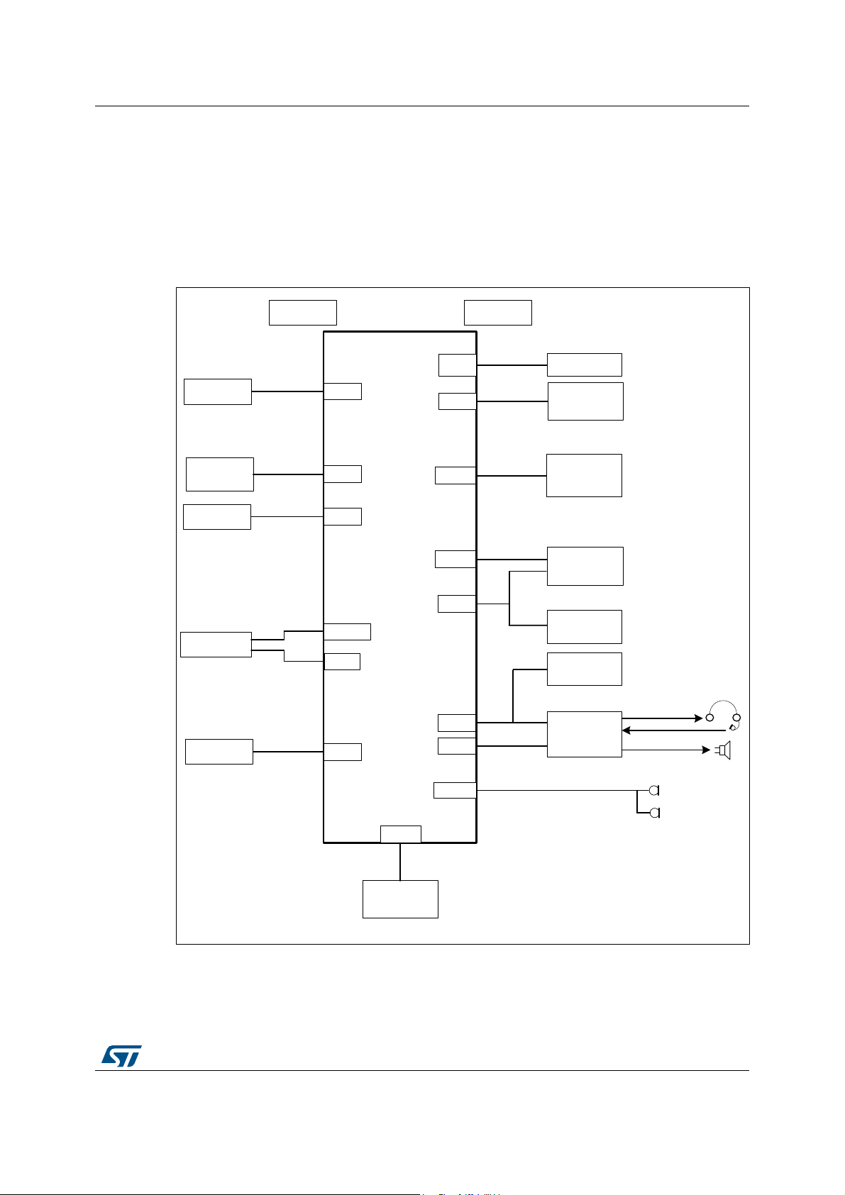
6 Hardware layout and configuration
The 32F412GDISCOVERY discovery kit is designed around the STM32F412ZGT6 (144-pin
TQFP package). The hardware block diagram showed in Figure 3, illustrates the
STM32F412ZGT6 connections with the peripherals. Figure 4 and Figure 5 show the
location of the main components on the discovery kit.
Figure 3. Hardware block diagram
DocID029078 Rev 2 9/48
47

Hardware layout and configuration UM2032
06Y9
88
'LJLWDO
PLFURSKRQHV
8
670)=*7
3
H[WHQVLRQ
FRQQHFWRU
&1
,
&
H[WHQVLRQ
FRQQHFWRU
-3
9''B86%
VRXUFH
VHOHFWLRQ
-3
9''B0&8
YROWDJH
VHOHFWLRQ
-3
,''
MXPSHU
&1
X6'
FRQQHFWRU
&1
$XGLRMDFN
&1
86%27*)6
0LFUR$%
FRQQHFWRU
%
5HVHW
EXWWRQ
==
/&'
3
H[WHQVLRQ
FRQQHFWRU
%
MR\VWLFN
&1&1
$UGXLQR
FRQQHFWRUV
-3
6XSSO\
VRXUFH
VHOHFWLRQ
&1
6:'
FRQQHFWRU
&1
67/,1.9
0LFUR%86%
FRQQHFWRU
&1
&1
$UGXLQR
FRQQHFWRUV
/'
9SRZHU
/('
/'/'/'
/'
8VHU/('V
/'
86%
)$8/7
/('
/'
$UGXLQR
/('
/'
67/,1.SRZHU
VZLWFK)$8/7
/'
9%86/('
&1
X6'FRQQHFWRU
&1
&DSDFLWLYH
7RXFK3DQHO
FRQQHFWRU
55
7RDGMXVWRXWSXWYROWDJH
RIUHJXODWRU8
Figure 4. 32F412GDISCOVERY top layout
Figure 5. 32F412GDISCOVERY bottom layout
10/48 DocID029078 Rev 2
06Y9

UM2032 Hardware layout and configuration
2
8
1
6
5
485
4
13
12
48
1
8
24
37
1
1
2
5
6
10
7
25
36
25
2
1
1
109
108
73
6
2
1
72
144
37
1 8
8 1
8
5
36
4
5
31
D
A
50
49
50
49
29
28
22
2
23
44
2261
50.8
172
5.08
22.86
65.68
59.35
4.06
23.79
67
48.26
6.1 32F412GDISCOVERY discovery kit mechanical drawing
Figure 6. 32F412GDISCOVERY mechanical drawing
6.2 Embedded ST-LINK/V2-1
ST-LINK/V2-1 programming and debugging tool is integrated into the
32F412GDISCOVERY discovery kit. Compared to ST-LINK/V2 stand-alone tool available
from STMicroelectronics, ST-LINK/V2-1 offers new features and drops some others.
New features:
• USB software re-enumeration
• Virtual COM port interface on USB
• Mass storage interface on USB
• USB power management request for more than 100 mA power on USB
Feature dropped:
• SWIM interface
For all general information concerning debugging and programming features common
between V2 and V2-1 versions, refer to ST-LINK/V2 in-circuit debugger/programmer for
STM8 and STM32 User manual (UM1075) at the www.st.com website.
DocID029078 Rev 2 11/48
47

Hardware layout and configuration UM2032
6.2.1 Drivers
Before connecting STM32F412ZGT6 to a Windows® XP, 7 or 8 PC via USB, a driver for
ST-LINK/V2-1 must be installed. It can be downloaded from the www.st.com website.
In case the 32F412GDISCOVERY discovery kit is connected to the PC before the driver is
installed, some 32F412GDISCOVERY interfaces may be declared as "unknown" in the PC
device manager. To recover from this situation the user must install the driver files, and
update the driver of the connected device from the device manager (see Figure 7).
Note: Prefer using the "USB Composite Device" handle for a full recovery.
Figure 7. USB composite device
6.2.2 ST-LINK/V2-1 firmware upgrade
ST-LINK/V2-1 employs a dedicated MCU with Flash memory. Its firmware determines
ST-LINK/V2-1 functionality and performance. The firmware may evolve during the life span
of the 32F412GDISCOVERY to include new functionalities, fix bugs or support new target
microcontroller families. It is therefore recommended to keep the
ST-LINK/V2-1 firmware up to date. The latest version is available from the www.st.com
website.
6.3 Power supply
6.3.1 Power supply sources
The 32F412GDISCOVERY discovery kit is designed to be powered by the following
sources:
• 5 V DC from the ST-LINK/V2-1 USB connector CN6 with 500 mA current limitation.
Power mechanism of supplying the discovery kit by the ST-LINK/V2-1 is explained in
Section 6.3.4: Supplying the 32F412GDISCOVERY through the ST-LINK/V2-1 USB
port. A jumper should be placed in location STLK of JP3, connecting pins 3 and 4. The
green LED LD6 is lighted on to confirm the presence of +5 V voltage.
• 5 V DC from the user USB FS connector CN3. A jumper should be placed in location
USB of JP3, connecting pins 5 and 6. The green LED LD6 is lighted on to confirm the
presence of +5 V voltage.
• 6 V to 9 V DC from VIN pin of Arduino Uno V3 compatible connector CN2. The voltage
is limited to 9 V to keep the temperature of the regulator U3 within his thermal safe
12/48 DocID029078 Rev 2

UM2032 Hardware layout and configuration
VOUT VREF 1 R92()R90()÷+()×=
area. A jumper should be placed in location E5V of jumper JP3, connecting pin 1 to pin
2 of JP3. The green LED LD6 is lighted on to confirm the presence of +5 V voltage.
• 5 V DC from +5 V pin of Arduino Uno V3 connector (CN2 pin 5) with limitations. The
jumpers on JP3 and CN5 have to be removed, SB21 (NRST) and SB28 (SWO) have to
be opened. In such configuration the ST-LINK/V2-1 MCU is not powered, as
consequence the 8 MHz of the ST-LINK/V2-1 cannot be used as external input clock
for the STM32.
For details on JP3 jumper setting refer to Table 2: Power-supply-related jumper settings.
6.3.2 STM32 power supply options
The 32F412GDISCOVERY offers the possibility to supply the STM32 under 2.0 V or 3.3 V.
A jumper has to be placed in location 2.0 V of JP5 to supply the STM32 under 2.0 V, then
pins 2 and 3 are connected. Similarly the jumper has to be placed in 3.3 V to supply the
STM32 with 3.3 V, then pins 1 and 2 of JP5 are connected.
For details on JP5 jumper setting refer to Table 2: Power-supply-related jumper settings.
6.3.3 Modification of STM32 voltage
Regulator U16 LD1117STR is dedicated to the 2.0 V supply. The output voltage of U16 is by
default 2.0 V but it is adjustable depending on the resistors R90 and R92 which are by
default 120 and 68 ohms respectively. The output voltage is calculated as following:
with VREF = 1.25 V.
If necessary, resistors R90 and R92 can be changed to modify the STM32 supply voltage.
R90 and R92 are easily located bottom side of the discovery kit near U16 (see Figure 5 and
Figure 8).
DocID029078 Rev 2 13/48
47

Hardware layout and configuration UM2032
Figure 8. R90 and R92 resistors
6.3.4 Supplying the 32F412GDISCOVERY through the ST-LINK/V2-1 USB port
To power the 32F412GDISCOVERY through the ST-LINK/V2-1, the USB host (a PC) gets
connected with the 32F412GDISCOVERY Micro-B USB receptacle CN6, via a USB cable.
This event starts the USB enumeration procedure. In its initial phase, the current supply
capability of the USB port located on the host, is limited to 100 mA. It is enough because
only the ST-LINK/V2-1 part of the 32F412GDISCOVERY discovery kit draws power at that
time. If the solder bridge SB18 is open (default configuration), the U8 ST890 power switch is
set to OFF position, and only the ST-LINK/V2-1 is powered. In the next phase of the
enumeration procedure, the host PC informs the ST-LINK/V2-1 facility of its capability to
supply up to 500 mA of current. If the answer is positive, the ST-LINK/V2-1 sets the U8
ST890 switch to ON position to supply power to the remainder of the 32F412GDISCOVERY
discovery kit. If the PC USB port is not capable of supplying up to 500 mA of current,
another power source should be used like VIN pin of connector CN2.
Should a short-circuit occur on the discovery kit, the ST890 power switch protects the USB
port of the host against current demand exceeding 600 mA. In such an event, the red LED
FAULT LD10 lights on.
The 32F412GDISCOVERY discovery kit can also be supplied from a USB power source not
supporting enumeration, such as a USB charger. In this particular case, SB18 solder bridge
must be closed. ST-LINK/V2-1 turns the ST890 power switch ON regardless of the
enumeration procedure result and passes the power unconditionally to the discovery kit.
The green LED LD6 turns on whenever the discovery kit is powered.
14/48 DocID029078 Rev 2

UM2032 Hardware layout and configuration
USB
STLK
E5V
1
USB
STLK
E5V
1
6.3.5 Programming/debugging when the power supply is not from ST-LINK/V2-1
Before connecting the USB cable from the ST-LINK/V2-1 USB connector CN6 to the PC, it
is mandatory to power the discovery kit using the user USB FS connector CN3 or the VIN
pin of the Arduino Uno V3 connector CN2. Proceeding this way, ensures that the
enumeration succeeds thanks to the external power source.
The following power sequence procedure must be respected:
1. Put a jumper in JP3 at location USB to use power from the user USB CN3 or at location
E5V to use power from VIN of Arduino Uno V3 connector CN2.
2. Connect the corresponding external power source.
3. Check that the green LED LD6 is turned ON
4. Connect the PC to the ST-LINK/V2-1 USB connector CN6
If this order is not respected, the discovery kit may be powered by VBUS first from STLINK/V2-1, and the following risks may be encountered:
1. If more than 500 mA current is needed by the discovery kit, the PC may be damaged or
current can be limited by PC. As a consequence the discovery kit is not powered
correctly.
2. 500 mA is requested at the enumeration. If the PC cannot provide such current there is
a risk that the request is rejected and the enumeration does not succeed.
6.3.6 Measurement of current IDD drawn by the microcontroller
The jumper JP7 should be closed by default to supply the STM32F412ZGT6. To measure
the current IDD drawn by the microcontroller STM32F412ZGT6 only, remove the jumper
JP7 and replace it by a multimeter (see Tabl e 2).
Jumper Description
JP3
Table 2. Power-supply-related jumper settings
Default Setting
32F412GDISCOVERY is supplied through the Micro-B ST-LINK/V2-1 connector
CN6. Jumper in STLK place.
32F412GDISCOVERY is supplied through CN3 Micro-AB USB FS connector.
Jumper in USB place.
DocID029078 Rev 2 15/48
47
Hardware layout and configuration UM2032
USB
STLK
E5V
1
USB
STLK
E5V
1
+3V3
1
+2V
+2V +3V3
1
VDD +3V3
1
Table 2. Power-supply-related jumper settings (continued)
Jumper Description
32F412GDISCOVERY is supplied through the VIN pin of the Arduino Uno V3
compatible connector CN2. Jumper in E5V place.
JP3
JP5
32F412GDISCOVERY is supplied by +5 V pin of Arduino
Uno V3 compatible
connector CN2 (pin 5) or by pins 3 or 4 of the extension connector P2. No jumper in
JP3.
Default Setting
STM32F412ZGT6 is supplied with a +3.3 V voltage (VDD_MCU).
STM32F412ZGT6 STM32 is supplied with a +2.0 V voltage (VDD_MCU).
Default Setting
VDD_USB power pin of STM32F412ZGT6 is supplied with same voltage VDD_MCU
as remainder supply pins of STM32.
JP6
16/48 DocID029078 Rev 2

UM2032 Hardware layout and configuration
VDD +3V3
1
IDD
Table 2. Power-supply-related jumper settings (continued)
Jumper Description
VDD_USB power pin of STM32F412ZGT6 is supplied with a fix voltage of +3V3
independently of the remainder of supply pins of STM32.
JP6
Default Setting
JP7 IDD is closed by default to supply the STM32F412ZGT6 and when removed, it
offers the possibility to insert an ammeter to measure the current drawn by the
STM32 only.
JP7
DocID029078 Rev 2 17/48
47

Hardware layout and configuration UM2032
6.4 Clock source
6.4.1 HSE clock source
By default the 8 MHz clock source is provided to the STM32F412ZGT6 by the MCO output
of the ST-LINK/V2-1 MCU U6. In that case the solder bridge SB20 is closed, resistors R45
and R46 are not soldered, solder bridge SB22 is open. The pins PH0 and PH1 are not
available for the extension connector P2.
Alternatively, the discovery kit offers the possibility to use a crystal to provide the 8 MHz
HSE clock source of the STM32F412ZGT6 U7. In that case, PH0 and PH1 are used as
OSC_IN and OSC_OUT respectively. The solder bridges SB20, SB22, SB16 must be
opened, 0 ohm resistors should be soldered to R45 and R46 and a crystal must be soldered
in place X2. Regarding component selection of X2, capacitors C19 and C21 (8.2 pF) are
optimized for a crystal NDK NX3225GD 8 MHz EXS00A-CG04874 and they are not fitted.
The pins PH0 and PH1 are not available for the extension connector P2.
6.4.2 LSE clock source
By default, the 32.768 kHz crystal X3 is connected to pins PC14-OSC32_IN and PC15OSC32_OUT of STM32F412ZGT6 for the RTC clock. Solder bridges SB25 and SB23 must
be open.
If LSE clock is not used, it is possible to use PC14-OSC32_IN and PC15-OSC32_OUT of
STM32F412ZGT6 and to access by the extension connector P2. In that case, solder
bridges SB25 and SB23 must be closed and resistors R54, R56 removed.
6.5 Reserved use of solder bridges
The following solder bridges must not be changed otherwise the microcontroller
STM32F412ZGT6 U7 or other parts of the discovery kit may be damaged:
• Solder bridges must be left closed: SB34, SB26
• Solder bridges must be left open: SB27, SB35
6.6 Reset source
The reset signal of 32F412GDISCOVERY discovery kit is low active and the reset sources
include:
• Reset button B1, providing solder bridge SB1 is closed (default setting)
• Embedded ST-LINK/V2-1, providing solder bridge SB21 is closed (default setting)
• Arduino Uno V3 compatible connector CN2 pin 3
• Extension connector P1 pin 6
18/48 DocID029078 Rev 2
UM2032 Hardware layout and configuration
6.7 Boot options
After reset, the STM32F412ZGT6 boots from the following embedded memory locations
depending on bits BOOT0 and BOOT1 (see Tab le 3 ):
• User Flash memory (non-protected)
• System Flash memory (protected) for In Circuit Programming
• RAM for debugging
BOOT0 BOOT1 Boot Memory
0 X User Flash
1 0 System Flash
11 RAM
BOOT0 is set by the input pin BOOT0 of the STM32F412ZGT6. Its level is set by default to
0 by closing the solder bridge SB31 and keeping R69 unfitted. BOOT1 is shared with the
GPIO PB2 used as QSPI_CLK and is sampled by the STM32F412ZGT6 only at RESET
phase. At start-up, BOOT1 level depends on the resistors R104 and R100. By default R100
and R104 are not fitted on the discovery kit to avoid any influence on the QSPI_CLK signal
using same pin as BOOT1.
Table 3. Boot options
The application note “STM32 microcontroller system memory boot mode” Application note
(AN2606) details the bootloader mechanism and configurations.
Boot-related solder bridge and resistor settings are reported in Table 4:
Resistors, solder bridge Description
SB31 Closed
R69 not fitted
BOOT0=0
SB31 Open
R69 fitted
(any value
from 0 to 10K)
BOOT0=1
1. To keep Quad-SPI functionality after boot-up phase, the user should select a resistor value of R100 or
R104 insuring a weak pull-down or weak pull-up respectively.
Table 4. Boot-related solder bridge and resistor settings
R100 and
R104 not fitted
BOOT1=X
R100 not fitted
R104 fitted
BOOT1=0
R100 fitted
R104 not fitted
BOOT1=1
Default Setting
Microcontroller STM32F412ZGT6 boots from user Flash.
Microcontroller STM32F412ZGT6 boots from system Flash.
(1)
R104 is a pull-down resistor on PB2 shared between BOOT1 and
QSPI_CLK.
(1)
Microcontroller STM32F412ZGT6 from RAM.
R100 is a pull-up resistor on PB2 shared between BOOT1 and
QSPI_CLK.
DocID029078 Rev 2 19/48
47

Hardware layout and configuration UM2032
6.8 Audio codec
A Cirrus/Wolfson codec WM8994 U15 connected to the I2S3 interface of the microcontroller
STM32F412ZGT6 offers possibility to connect a stereo headphone or headset with a monoanalog microphone. A loudspeaker can be connected to the extension connector.
The digital audio output from the microcontroller is handled by the port of the microcontroller
PB5 called CODEC_I2S3_SD while the other direction is handled by port PB4 called
CODEC_I2S3ext_SD.
²
The I
C-bus address of WM8994 is 0b0011010.
6.8.1 Stereo headset and headphone jack
A stereo headphone or a stereo headset with analog microphone can be plugged into the
3.5 mm standard jack socket CN9.
The stereo digital audio streamed from pin PB5 of the microcontroller STM32F412ZGT6 is
transformed in a stereo analog output by the codec WM8994 and is delivered to the
headphone or headset through the pins 6 and 4 of the jack socket CN9.
If a headset is plugged into CN9, the bias of the microphone is driven by the output
MICBIAS1 of the codec and the analog audio enters into the codec by the pin IN1LN.
The corresponding digital audio output from the codec is connected to the microcontroller
STM32F412ZGT6 by the port PB4.
6.8.2 Loudspeaker output
The 32F412GDISCOVERY discovery kit can deliver a monophonic audio to a loudspeaker
connected to pins 36 and 38 of the extension connector P2. It is recommended to use the
WM8994 codec loudspeaker outputs SPKOUTRN and SPKOUTRP in linear mode called
"class AB". This mode is compatible with 4-ohm to 8-ohm impedance loudspeakers. Use of
the switching mode called "class D" requires to use an appropriate filter to maximize
rejection of unwanted frequencies and efficiency. To select the mode "class AB" of the codec
WM8994, set to 1 the bit 8 of the register 0x23.
6.9 Digital microphones
Two ST-MEMS MP34DT01TR digital microphones U4 and U5 are available on the
32F412GDISCOVERY discovery kit. The two microphones are located at a distance of
21 mm each other. The microphones are connected to the DFSDM of the STM32 by the port
PC2 generating the clock and by the port PB1 collecting the PDM interleaved data.
6.10 USB OTG FS
A USB OTG full-speed communication is available at USB Micro-AB receptacle connector
CN3.
Limitations: the USB-related operating supply voltage of STM32L412ZGT6 (VDD_USB
line) must be within the range from 3.0 V to 3.6 V. Therefore, in case the STM32F412ZGT6
is supplied with 2 V by JP5 set in +2 V position, the USB of the STM32 works only if the
VDD_USB power pin is supplied independently by +3.3V. This is done by closing pins 2 and
3 of the jumper JP6 (refer to Table 2: Power-supply-related jumper settings).
20/48 DocID029078 Rev 2

UM2032 Hardware layout and configuration
6.10.1 32F412GDISCOVERY is USB device
When the 32F412GDISCOVERY is USB device, the discovery kit is powered by the 5 V of
the CN3 USB OTG FS Micro-AB connector. In this case a jumper must be put in USB
location of jumper JP3 and the green LEDs LD7 VBUS and LD6 PWR light on to confirm the
5 V presence.
6.10.2 32F412GDISCOVERY is USB host
When the 32F412GDISCOVERY is USB host it supplies the 5V for the USB peripheral
using one of the following sources:
• ST-LINK/V2-1 USB Micro-B connector CN6, putting a jumper in STLK location of JP3
• An external +5 V source connected to pins 3 or 4 of the extension connector P2, with
no jumper in JP3.
• An external +5V source connected to 5 V pin of Arduino Uno V3 connector CN2, with
no jumper in JP3.
• An external source between +7 to +11 V connected to VIN pin of Arduino Uno V3
connector CN2, putting a jumper in E5V location of JP3.
The green LED LD6 is lighted to confirm the presence of the +5 V source.
The power switch STMPS2141STR is controlled by the port PG8 of STM32 to deliver the
5 V power to the USB device connected to the USB connector CN3. It is recommended to
use PG8 in open drain mode. When PG8 is closed to ground, the power switch is closed,
and the green LED LD7 confirms the 5 V to the USB Device.
The red LED LD8 FAULT is lit when an overcurrent occurs.
For more details refer to Section 6.3: Power supply.
6.11 microSD card
microSD cards with a capacity of 4 Gbytes or more can be inserted in the receptacle CN13.
The four bits of the SDIO interface including CLK and CMD signals of the STM32F412ZGT6
are used to communicate with the microSD card. The card detection is read by the GPIO
PD3: when a microSD card is inserted, the logic level is 0, otherwise it is 1.
Note that port PC9 used as uSD_D1 can be routed also to the pin 46 of the extension
connector P2, by closing the solder bridge SB43 for other usage like the alternate function
MCO2. Therefore the use of the microSD card is exclusive with MCO2 output.
Limitations: The microSD card is not working when the STM32 is supplied with 2V.
6.12 I2C extension connector
The I2C2 bus is available on the I2C extension connector CN10. I2C2-SDA (port PB9) is
available on pin 1 and I2C2-SCL is available on pin 3. Pins 5 and 7 of CN10 are the VDD
and GND supplying the microcontroller. I2C2 voltage levels follows also VDD.
DocID029078 Rev 2 21/48
47
Hardware layout and configuration UM2032
6.13 Quad-SPI NOR Flash memory
A 128-Mbit Quad-SPI NOR Flash memory (N25Q128A13EF840E from MICRON) is
connected to the Quad-SPI interface of the STM32F412ZGT6 microcontroller.
Note that QSPI_CLK (port PB2) is sampled by the STM32F412ZGT6 at start-up as the
BOOT1 bit. If necessary, the user can set the BOOT1 state by fitting one of the resistors
R100 or R104. By default R100 and R104 are not fitted. Refer to Section 6.7: Boot options
for more details.
Limitations: The Quad-SPI memory is not working when the STM32 is supplied with 2 V.
6.14 Virtual COM port
The serial interface USART2 is directly available through a USB virtual COM port of the
ST-LINK/V2-1. The USB connector is CN6.
6.15 Arduino Uno V3 connectors
CN1, CN2, CN11 and CN12 are female connectors compatible with Arduino Uno V3
standard. Most shields designed for Arduino Uno V3 can fit to the 32F412GDISCOVERY
discovery kit.
Caution: The IOs of STM32 microcontroller are 3.3 V compatible instead of 5 V for Arduino Uno V3.
Left connectors Right connectors
CN No.
- - - - - I2C2_SCL PB10 D15 10
--- - - AVDD-AVDD8
- - - - - Ground - GND 7
CN2
Power
Pin
Pin name STM32 pin Function Function
No.
1- -
2 IOREF - 3.3 V SPI1_MISO PA6 D12 5
3 NRST NRST Reset
Table 5. Arduino Uno V3 compatible connectors
STM32
pin
-I2C2_SDAPB9D149
Not
connected
SPI1_SCK PA5 D13 6
TIM3_CH2,
SPI1_MOSI
PA7 D11 4
Pin
name
Pin No. CN No.
CN12
Digital
22/48 DocID029078 Rev 2
UM2032 Hardware layout and configuration
Table 5. Arduino Uno V3 compatible connectors (continued)
Left connectors Right connectors
CN No.
CN2
Power
--- - -TIM5_CH1PF3D67
CN1
Analog
Pin
Pin name STM32 pin Function Function
No.
+3.3 V
4+3V3 -
5+5 V -
6 GND - Ground - PG10 D8 1
7 GND - Ground - - - -
8VIN -
1 A0 PA1 ADC1_IN1 TIM5_CH4 PF10 D5 6
2 A1 PC1 ADC1_IN11 - PG12 D4 5
3 A2 PC3 ADC1_IN13 TIM5_CH2 PF4 D3 4
4 A3 PC4 ADC1_IN14 - PG13 D2 3
5A4
6A5
PC5 or PB9
(see Note:3)
PB0 or PB10
(see Note:3)
input/output
(see Note:1)
+5 V
input/output
(see Note:4)
+6V to +9V
power input
(see Note:2)
ADC1_IN15
or
I2C2_SDA
(see Note:3)
ADC1_IN8
or
I2C2_SCL
(see Note:3)
TIM2_CH1,
SPI1_NSS
TIM4_CH3 PB8 D9 2
-PG11D78
USART6_TX PG14 D1 2
USART6_RX PG9 D0 1
STM32
pin
PA15 D 10 3
Pin
name
Pin No. CN No.
CN12
Digital
CN11
Digital
Note:1 Important, before using pin 4 of CN2 as +3.3V input, insure that the solder bridge SB4 is
removed. Otherwise the 32F412GDISCOVERY discovery kit could be damaged by the
overcurrent.
Note:2 The external voltage applied to pin VIN should be in the range 6 to 9V at 25°C ambient
temperature. If a higher voltage is applied, the regulator U3 may overheat and could be
damaged.
Note:3 By default pin 5 and pin 6 of connector CN1 are connected respectively to the port PC5
(ADC1_IN15) and BP0 (ADC1_IN8) of the STM32. They are enabled by the default
configuration of the solder bridges: SB8 and SB6 closed, SB7 and SB5 opened. In case it is
necessary to have an I2C interface instead of ADC inputs on pins 5 and 6 of CN1, open SB8
and SB6, and close SB7 and SB5.
Note:4 Important, before using pin 4 of CN2 as +5 V input, insure the jumpers and solder bridges
are configured according to 5
V DC power input defined in Section 6.3.1: Power supply
sources. Otherwise the 32F412GDISCOVERY discovery kit could be damaged by the
overcurrent.
DocID029078 Rev 2 23/48
47
Hardware layout and configuration UM2032
6.16 Extension connectors P1 and P2
The extension connectors consist in male pin headers P1 and P2 (not soldered by default).
They provide access to the following IPs of the STM32F412ZGT6:
• SPI
2
• I
C with SMBA and FM+ (1 MHz speed)
• Full USART (Rx, Tx, RTS, CTS)
• CAN
• ADC inputs
• TIMERs channels
2
• I
S full duplex with SD and extSD alternate functions.
• DFSDM input for stereo PDM digital microphones
Most of the ports connected to the extension connectors P1 and P2 are the same for the
32F401CDISCOVERY and 32F411EDISCOVERY discovery kits, to maximize the
compatibility with the previous designs. In Tab l e 6, Tab le 7 and in the 32F412GDISCOVERY
schematics (see Section Appendix A: Schematics), the pin numbers corresponding to these
ports, are annotated with the star symbol: “*”.
In Table 6, Table 7 and in the 32F412GDISCOVERY schematics (see Section Appendix A:
Schematics) the pins belonging to the extension connectors P1 and P2 annotated with a
letter, are shared with a peripheral of the 32F412GDISCOVERY (for example, S means that
the port PC9 corresponding to pin 46 is also used for microSD, see Table 7).
Table 6. Pin assignment for the extension connector P1
P1 odd pins P1 even pins
Pin No. Name Note Pin No. Name Note
1GND* 2GND*
3 VDD_MCU * 4 VDD_MCU *
5 GND * 6 NRST *
7 PC1 *A 8 PC0 *
9PC3*A10PC2*D
11 PA1 * A 12 - -
13 PA3 *V 14 PA2 *V
15 PA5 *A 16 PA4 *C
17 PA7 *A 18 PA6 *A
19 PC5 *A 20 PC4 *A
21 PB1 *D 22 PB0 *A
23 GND * 24 PF2 -
25 PF3 A 26 - -
27 PF10 A 28 PF11 -
29 - - 30 PF13 -
31 PG2 C 32 - -
24/48 DocID029078 Rev 2
UM2032 Hardware layout and configuration
Table 6. Pin assignment for the extension connector P1 (continued)
P1 odd pins P1 even pins
Pin No. Name Note Pin No. Name Note
33 PG9 A 34 PB10 *A
35 PB11 *D 36PB12*C
37 PB13 * 38 PB14 *
39 PB15 * 40 - -
41 - - 42 - -
43 - - 44 PD12 *
45 PD13 * 46 - -
47 - - 48 - -
49 GND * 50 GND *
Table 7. Pin assignment for the extension connector P2
P2 odd pins P2 even pins
Pin No. Name Note Pin No. Name Note
1GND* 2GND*
3+5V* 4+5V*
5+3V3* 6+3V3*
7PH0* 8PH1*
9 PC14 * 10 PC15 *
11 PE6 * 12 PC13 *
13 PE4 * 14 PE5 *
15 PE2 * 16 PE3 *
17 PE0 * 18 PE1 *
19 PB8 *A 20 PB9 *A
21 BOOT0 * 22 VDD_MCU *
23 PB6 *TC 24 PB7 *TC
25 PB4 *C 26 PB5 *C
27 - - 28 PB3 *
29 - - 30 PD6 *
31 PG10 A 32 PG11 A
33 PG12 A 34 PG13 A
35 PG14 A 36 SPKOUTRN -
37 - - 38 SPKOUTRP -
39 PA14 * 40 PA15 *A
DocID029078 Rev 2 25/48
47

Hardware layout and configuration UM2032
Table 7. Pin assignment for the extension connector P2 (continued)
P2 odd pins P2 even pins
Pin No. Name Note Pin No. Name Note
41 PA10 * 42 PA13 *
43 PA8 *D 44 - -
45 - - 46 PC9 *S
47 PC6 * 48 PC7 *C
49 GND * 50 GND *
Note:1 The star symbol “*” means pin compatible with 32F401CDISCOVERY and
32F411EDISCOVERY discovery kits.
Note:2 Meaning of the letters: “A”: shared with Arduino Uno V3 connectors, C: shared with codec,
D: shared with digital microphones, V: shared with virtual COM port, T: shared with
capacitive touch panel, S: shared with microSD.
6.17 LCD display, backlight and touch panel
6.17.1 LCD display
The display is a 1.54-inch, 240x240 pixels TFT color LCD with capacitive touch panel. It
displays up to 262 K colors. The LCD parallel interface is connected to the FMC of the
STM32F412ZGT6 by the connector CN15 (see Tab le 8 ).
To enable the data bus of the LCD display in 16-bit mode, the solder bridges SB41 and
SB42 are opened and closed respectively by default. In this way the IM signal of the LCD is
set to high.To use the LCD in 8-bit mode, SB41 must be closed and SB42 opened.
The selection of the LCD is performed by FMC_NE1 (PD7), write-enable signal is
FMC_NWE (PD5) and read-enable is FMC_NOE (PD4). The address bit A0 of the FMC
(Flexible Static Memory Controller) is used to select data/command access to the LCD.
The port PG4 should be used as an input of the microcontroller connected to the LCD signal
TE (Tearing Effect). To avoid visible artifacts on the display, TE signal is used to synchronize
the refresh of the LCD memory done by the microcontroller with the LCD scan.
The port PD11 of the STM32F412ZGT6 controls the reset of the LCD display LCD_RESET.
CN15 pin
1 GND Ground GND
2 LCD_TE Tearing Effect output pin to send an interrupt to STM32 PG4
3 D15 Data connected to FMC PD10
4 D14 Data connected to FMC PD9
Signal
name
Table 8. Pin assignment for connector CN15
Description
STM32 pin
involved
5 D13 Data connected to FMC PD8
26/48 DocID029078 Rev 2

UM2032 Hardware layout and configuration
Table 8. Pin assignment for connector CN15 (continued)
CN15 pin
Signal
name
Description
6 D12 Data connected to FMC PE15
7 D11 Data connected to FMC PE14
8 D10 Data connected to FMC PE13
9 D9 Data connected to FMC PE12
10 D8 Data connected to FMC PE11
11 D7 Data connected to FMC PE10
12 D6 Data connected to FMC PE9
13 D5 Data connected to FMC PE8
14 D4 Data connected to FMC PE7
15 D3 Data connected to FMC PD1
16 D2 Data connected to FMC PD0
17 D1 Data connected to FMC PD15
18 D0 Data connected to FMC PD14
19 /RD Read of LCD connected to FMC_NOE PD4
20 /WR Write of LCD connected to FMC_NWE PD5
21 RS Data/Command select connected to A0 PF0
22 /CS Chip Select of LCD connected to FMC_NE1 PD7
STM32 pin
involved
23 RESET LCD RESET PD11
24 IM 8-bit (low)/16-bit (high) mode selection pin n/a
25 IOVCC LCD I/Os power supply connected to VDD n/a
26 VCI Power supply connected to +3.3V n/a
27 GND Ground GND
28 LEDA Anode of backlight LED n/a
29 LEDK Cathode of backlight LED n/a
6.17.2 LCD signal access (CN7)
CN7 is the footprint of a dual-row, through-hole, 26-pin header with 2.54 mm pitch. The
header CN7 gives an easy access to the FMC signals of the LCD (see Table 9).
CN7 odd pins Signal name CN7 even pins Signal name
1 A0 2 LCD_BLCTRL
3FMC_NWE 4 GND
5 FMC_NE1 6 FMC_NOE
7D08 D1
Table 9. Pin assignment for connector CN7
DocID029078 Rev 2 27/48
47

Hardware layout and configuration UM2032
Table 9. Pin assignment for connector CN7 (continued)
CN7 odd pins Signal name CN7 even pins Signal name
9 D2 10 +3.3V
11 D3 12 VD D
13 LCD_TE 14 LCD_RESET
15 D4 16 D5
17 D6 18 D7
19 D8 20 D9
21 D10 22 D11
23 D12 24 D13
25 D14 26 D15
6.17.3 Backlight
LEDK and LEDA signals of the LCD module are the cathode and the anode respectively of
the backlight LEDs.
The backlight requires a current source of typically 15 mA capable to deliver a voltage up to
10 V. This function is handled by the backlight-driver circuit STLD40DPUR that is a
switching-mode-boost converter, supplied by the +5 V rail of the discovery kit.
The high level on the signal LCD_BLCTRL (PF5) lights the backlight on. It is possible to dim
the backlight intensity by applying a low-frequency PWM signal to LCD_BLCTRL (1 to
10 kHz).
6.17.4 Touch panel
The touch panel is a capacitive touch panel using an I2C interface. The 10-pin connector
CN14 of the touch panel is located at the bottom side of the discovery kit (see Figure 5:
32F412GDISCOVERY bottom layout). The I
SCL line is connected to PB6. An interrupt output CTP_INT is connected to port PG5 to be
used as an interruption input of the microcontroller. Port PF12 is the reset of the capacitive
touch panel.
6.18 Joystick and LEDs
The blue button B2 is a 4-direction joystick with a selection mode when pressed in the
center. The logic state is high when one of the five-position switches (Left, Right, Up, Down,
Selection) is pressed. The center position is connected to a wake-up pin of the
microcontroller PA0. This offers the possibility to wake-up the microcontroller by pressing
the center of the joystick.
Four LEDs located near the Arduino Uno V3 connectors CN1 and CN2 are available for the
user (refer to the Figure 4: 32F412GDISCOVERY top layout). From left to right the user
finds LD1, LD2, LD3 and LD4 with their colors green, orange, red and blue respectively. To
light a LED a low-logic state 0 must be written in the corresponding GPIO.
2
C SDA line is connected to PB7 and the I2C
Table 10 gives the assignment of control ports to the LED indicators.
28/48 DocID029078 Rev 2

UM2032 Hardware layout and configuration
Table 10. Port assignment to the LED indicators
LED Controlled by STM32 port Color
LD1 PE0 Green
LD2 PE1 Orange
LD3 PE2 Red
LD4 PE3 Blue
DocID029078 Rev 2 29/48
47

Connectors UM2032
069
7 Connectors
7.1 I2C extension connector CN10
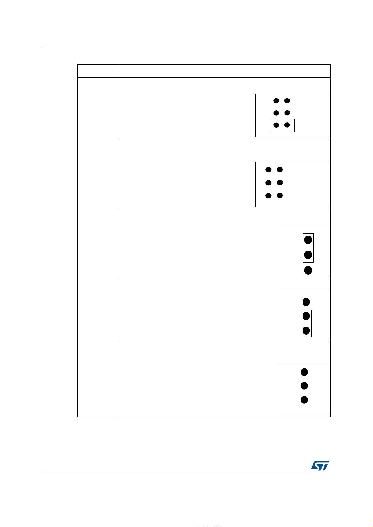
Figure 9. I2C extension connector CN10 (front view)
Pin number Description Pin number Description
1 I2C1_SDA (PB9) 5 VDD
2NC6NC
3 I2C1_SCL (PB10) 7 GND
4 EXT_RESET (PF11) 8 NC
Tab l e 11. I2C extension connector pinout CN10
7.2 USB OTG FS Micro-AB connector CN3
Figure 10. USB OTG FS Micro-AB connector CN3 (front view)
Pin number Description Pin number Description
1 VBUS (PA9) 4 ID (PA10)
2 DM (PA11) 5 GND
3 DP (PA12) - -
Table 12. USB OTG FS Micro-AB connector CN3
30/48 DocID029078 Rev 2

UM2032 Connectors
7.3 microSD connector CN13
Figure 11. microSD connector CN13 (front view)
Pin
number
1 SDIO_D2 (PC10) 6 GND
2 SDIO_D3 (PC11) 7 SDIO_D0 (PC8)
3 SDIO_CMD (PD2) 8 SDIO_D1 (PC9)
4+3.3V9GND
5 SDIO_CLK (PC12) 10 MicroSDcard_detect (PD3)
Table 13. microSD connector CN13
Description
Pin
number
7.4 ST-LINK/V2-1 USB Micro-B connector CN6
Figure 12. USB Micro-B connector CN6 (front view)
Description
DocID029078 Rev 2 31/48
47

Connectors UM2032
Table 14. USB Micro-B connector CN6
Pin number Description Pin number Description
1 VBUS (power) 4 GND
2 DM 5,6 Shield
3DP- -
32/48 DocID029078 Rev 2

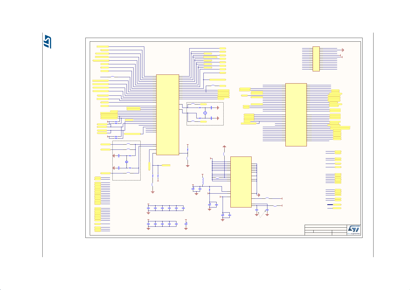
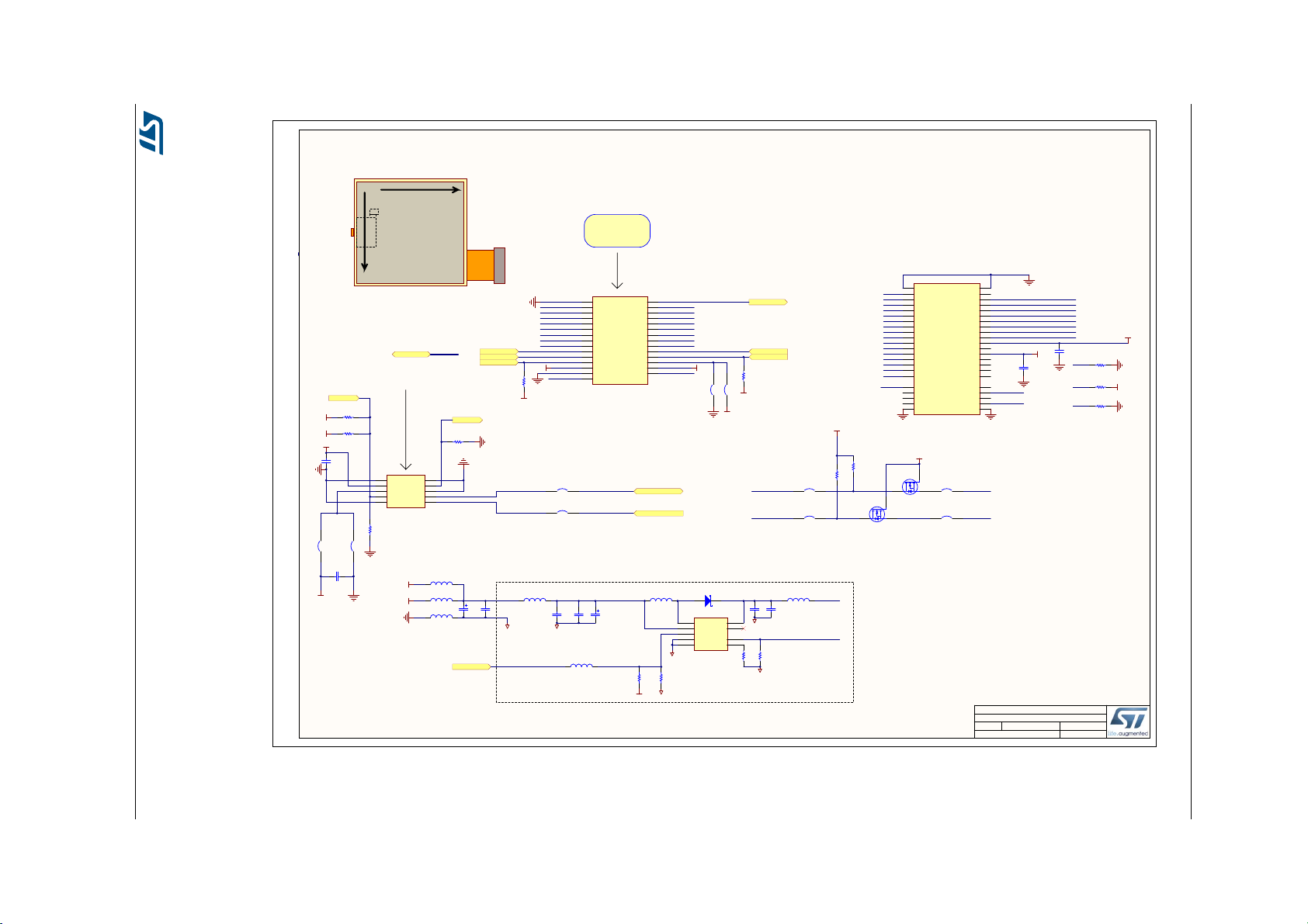
UM2032 Schematics
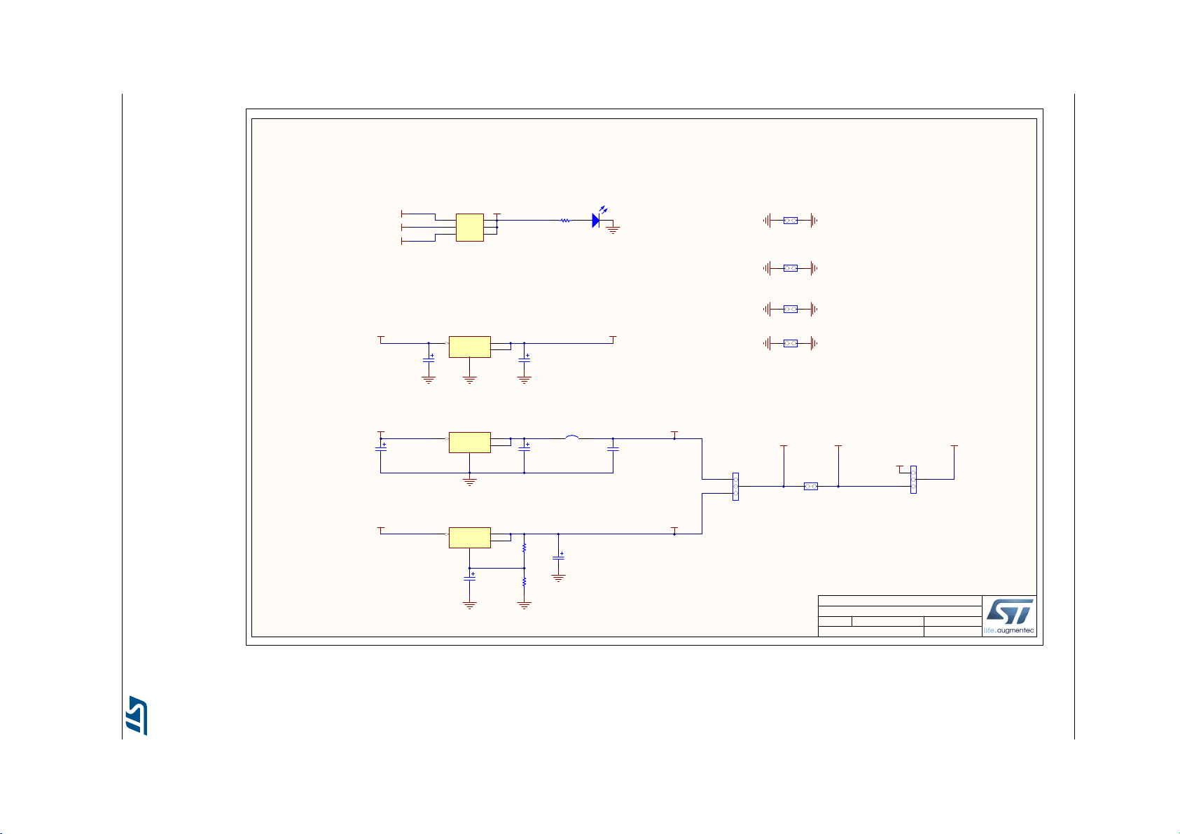
Appendix A Schematics
This section provides the design schematics for the 32F412GDISCOVERY discovery kit, to
help users to implement these features in application designs.
This section includes:
• Overall schematics for the 32F412GDISCOVERY, see Figure 13
• STM32 connections, see Figure 14
• Power supply, see Figure 15
• LCD, camera and connector, see Figure 16
• Quad-SPI, see Figure 17
• Audio amplifier, see Figure 18
• Peripherals, see Figure 19
• USB OTG FS, see Figure 20
• Extension connectors, see Figure 21
• Arduino Uno V3 connector, see Figure 22
• ST-LINK/V2-1, see Figure 23
DocID029078 Rev 2 33/48
47

34/48 DocID029078 Rev 2
111
MB1209-TOP
MB1209 D-02
6/29/2016
Title:
Size: Reference:
Date: Sheet: of
A3
Revision:
STM32F412G-DISCO
Project:
uSD_D0
uSD_D1
uSD_D2
uSD_D3
uSD_CLK
uSD_CMD
D[0..15]
A0
NRST
QSPI_BK1_IO3
FMC_NOE
FMC_NWE
LED3
LED4
QSPI_BK1_IO2
QSPI_BK1_IO0
QSPI_BK1_IO1
uSD_Detect
USB_OTGFS_VBUS
USB_OTGFS_ID
USB_OTGFS_DM
DFSDM_DATIN0
QSPI_CLK
DFSDM_CKOUT
FMC_NE1
LCD_RESET
LED1
LED2
JOY_RIGHT
JOY_LEFT
JOY_UP
JOY_DOWN
QSPI_BK1_NCS
USB_OTGFS_OVRCR
USB_OTGFS_PPWR_EN
SWO
SWDIO
SWCLK
USART2_TX
USART2_RX
EXT_RESET
PH0
PH1
STLK_MCO
JOY_SEL
CODEC_INT
LCD_TE
LCD_BLCTRL
PC0
PC2
PD12
PC1
PC3
PD13
PE6
PE4
PE2
PE0
PE1
PE5
PE3
PD6
PA4
PA6
PA2
PA1
PA7
PA5
PA3
PA14
PA10
PA8
PA13
PA15
PB10
PB12
PB14
PB11
PB13
PB15
PB8
PB6
PB4
PB7
PB5
PB3
PB9
PC4
PC5
PC14
PC6
PC15
PC7
PB1
PB0
PF2
PF3
PF10
PF11
PF13
PG2
PG9
PG10
PG11
PG12
PG13
PG14
I2C2_SDA
I2C2_SCL
USB_OTGFS_DP
PC13
BOOT0
DFSDM_DATIN3
I2C1_SCL
I2C1_SDA
CODEC_I2S3_WS
CODEC_I2S3_SCK
CODEC_I2S3_SD
CODEC_I2S3_MCK
CODEC_I2S3ext_SD
CTP_INT
ARD_D3
CTP_RST
ARD_D5
ARD_D4
ARD_A0
ARD_D2
ARD_D1
ARD_D0
ARD_D8
ARD_D7
ARD_A1
ARD_A2
ARD_A3
ARD_A4
ARD_D12
ARD_D13
ARD_D11
ARD_D10
ARD_A5
ARD_D15
ARD_D14
ARD_D9
ARD_D6
PC9
U_MCU2
MCU2.SchDoc
PC0
PC2
PA4
PA6
PC4
PB0
PB10
PB12
PB14
PD12
PC1
PC3
PA1
PA7
PC5
PB1
PA5
PB11
PB13
PB15
PD13
PH1
PC15
PC13
PE1
PB7
PB5
PB3
PE5
PE3
PB9
PD6
PA13
PA15
PC7
PH0
PC14
PE6
PE4
PE2
PE0
PB8
PB6
PA14
PA10
PA8
PB4
PC6
PA2
PA3
PF2
PF3
PF10
PF11
PF13
PG2
PG9
PG10
PG11
PG12
PG13
PG14
SPKOUTRN
SPKOUTRPBOOT0
NRST
PC9
U_Extension_connectors
Extension_connectors.SchDoc
CODEC_INT
DFSDM_DATIN0
DFSDM_CKOUT
SPKOUTRN
SPKOUTRP
DFSDM_DATIN3
CODEC_I2S3_SCK
CODEC_I2S3_WS
CODEC_I2S3_SD
I2C1_SCL
CODEC_I2S3_MCK
I2C1_SDA
CODEC_I2S3ext_SD
U_Audio
Audio.SchDoc
NRST ARD_A0
ARD_A1
ARD_A2
ARD_A3
ARD_A4
ARD_A5
ARD_D5
ARD_D4
ARD_D3
ARD_D2
ARD_D1
ARD_D0
ARD_D13
ARD_D12
ARD_D11
ARD_D10
ARD_D9
ARD_D8
ARD_D6
ARD_D7
ARD_D15
ARD_D14
U_Arduino_ Connectors
Arduino_ Connectors.SchDoc
LCD_RESET
A0
FMC_NWE
FMC_NOE
FMC_NE1
LCD_TE
LCD_BLCTRL
LCD_D[0..15]
I2C1_SDA
I2C1_SCL
CTP_INT
CTP_RST
U_LCD
LCD.SchDoc
uSD_CLK
uSD_CMD
uSD_D0
uSD_D1
uSD_D2
uSD_D3
uSD_Detect
EXT_RESET
LED1
LED2
LED3
LED4
NRST
I2C2_SDA
I2C2_SCL
JOY_SEL
JOY_DOWN
JOY_LEFT
JOY_RIGHT
JOY_UP
U_Peripherals
Peripherals.SchDoc
QSPI_BK1_IO0
QSPI_BK1_IO2
QSPI_BK1_IO1
QSPI_BK1_IO3
QSPI_CLK
QSPI_BK1_NCS
U_QSPI
QSPI.SchDoc
USB_OTGFS_VBUS
USB_OTGFS_DM
USB_OTGFS_DP
USB_OTGFS_ID
USB_OTGFS_OVRCR
USB_OTGFS_PPWR_EN
U_USB_OTG_FS
USB_OTG_FS.SchDoc
U_Power
Power.SchDoc
STLK_MCO
NRST
SWCLK
SWDIO
SWO
USART2_TX
USART2_RX
U_ST_LINK_V2-1_2
ST_LINK_V2-1_2.SCHDOC
i
FMCMatched Net Lengths [Tolerance = 200mil]
Impedance Constraint [Min = 40.00 Max = 60.00 ]
i
FMC
i
FMC
i
FMC
i
FMC
i
FMC
i
QSPI
Matched Net Lengths [Tolerance = 100mil]
i
QSPI
i
QSPI
i
QSPI
i
QSPI
i
QSPI
N
Figure 13. 32F412GDISCOVERY discovery kit
rev D-01 modifications:
Silkscreen:
- update revision of board to D top side and bottom side.
- name of pin32 of connector P1 is NC
- bottom side update the LCD reference: LCD ref:
FRD154BP2902-CTP
Schematic:
- R69-2 connected to VDD
- updated CTP connector CN14: pin8 is now IOVCC
- added SB44, SB45,
C87 connected to CN14 pin8
- remove ZZ2 because LCD and CTP are now same part
- updated reference of LCD ZZ1: FRD154BP2902-CTP ( now
LCD+CTP)
- added comment: CTP working with VDD_MCU from 1.8 to
3.6V
- added R105 100K to insure CTP INT is low at power-on.
- removed R11
-
pin26 of U6 STLINK, corrected name of power
+3V3_ST_LINK
- SB32 set: open by default
rev D-02 modifications:
- connected CN7 pin2 to PF5
- added two pull-up resistors to Reset of CTP one to VDD,
second one to +3V3. Not populated.
ote: Text in italic placed on a wire is not the net name. It just helps to identify rapidly
MCU IO related to this wire.
Schematics UM2032
211
MCU
MB1209 D-02
6/29/2016
Title:
Size: Reference:
Date: Sheet: of
A3
Revision:
STM32F412G-DISCO
Project:
PA4
PA5
PA6
PA7
PA10
PA0
PA1
PA15
PA3
PA13
PA14
PA2
PA8
PB5
PB7
PB14
PB15
PB10
PB8
PB9
PB1
PB2
PB3
PB0
PB4
PB11
PB12
PB13
PC0
PC2
PC3
PC4
PC5
PC6
PC7
PC8
PC9
PC10
PC11
PC12
PC13
I2C1_SCL
I2C1_SDA
uSD_D0
uSD_D1
uSD_D2
uSD_D3
uSD_CLK
C23
1.5pF
C30
1.5pF
R54
0
R56
0
C21 8.2pF
C19 8.2pF
R46
[N/A]
PH0-OSC_IN
PH1-OSC_OUT
PD0
PD1
PD2
PD3
PD4
PD5
PD6
PD7
PD8
PD9
PD10
PD12
PD13
PD14
PD15
D2
D3
D13
D14
D15
D0
D1
uSD_CMD
PE0
PE14
PE15
PE9
PE8
PE11
PE10
PE12
PE13
PE1
PE3
PE4
PE5
PE7
PF0
PF14
PF15
PF9
PF8
PF11
PF10
PF12
PF13
PF2
PF3
PF4
PF5
PF6
PF7
D4
D5
D6
D7
D8
D9
D10
D11
D12
A0
D[0..15]
A0
D[0..15]
A0
NRST
NRST
BOOT0
VDD_MCU
VDDA
VREF+
L1
BEAD
VDD_MCU
C8
2.2uF
C31
2.2uF
Ceramic capacitor (Low ESR)
C58
100nF
C76
100nF
C59
100nF
C15
1uF
C17
100nF
C10
1uF
C11
100nF
VDD_MCU
C60
100nF
C20
100nF
C75
100nF
C74
100nF
C73
100nF
VDD_MCU
C57
100nF
C68
100nF
C71
100nF
VDD_MCU
C9
4.7uF
VDD
PA0 - WKUP1
PA6
PA7
PA8- MCO1
PC1
PC2
PC3
PC4
PC5
PC8
R68
510
X3
NDK NX3215SA-32.768KHZ-EXS00A-MU00525
VDD_USB33
PE2
PE6
ARDUINO USART6_TX
ARDUINO USART6_RX
R69
[N/A]
QSPI_BK1_IO3
FMC_NOE
FMC_NWE
LED3
ARD_D5
ARD_D4
ARD_A0
ARD_D2
ARD_D1
ARD_D0
ARD_D8
ARD_D7
ARD_A1
ARD_A2
ARD_A3
ARD_A4
CODEC_I2S3_WS
R66 1K2
R67 1K2
VDD
PA1
PA2
PA4
PC9
PC10
PC11
PC12
SB31
Closed by default
VDD
LED4
PC13PC13-ANTI_TAMP
7
PC0
26
PC1
27
PC2
28
PC3
29
PA0-WKUP
34
PA1
35
PA2
36
PA3
37
PA4
40
PA5
41
PA6
42
PA7
43
PC4
44
PC5
45
PB0
46
PB1
47
PB2
48
PB10
69
PB11
70
PB12
73
PB13
74
PB14
75
PB15
76
PC6
96
PC7
97
PC8
98
PC9
99
PA8
100
PA9
101
PA10
102
PA11
103
PA12
104
PA13
105
PA14
109
PA15
110
PC10
111
PC11
112
PC12
113
PB3
133
PB4
134
PB5
135
PB6
136
PB7
137
PB8
139
PB9
140
PC14-OSC32_IN
8
PC15-OSC32_OUT
9
PH0-OSC_IN
23
PH1-OSC_OUT
24
NRST
25
BOOT0
138
PDR_ON
143
U7A
STM32F412ZGT6U
QSPI_BK1_IO2
QSPI_BK1_IO0
QSPI_BK1_IO1
ARD_D12
ARD_D13
PA5
ARD_D11
uSD_Detect
USB_OTGFS_VBUS
PA9
USB_OTGFS_ID
PA11
PA12
USB_OTGFS_DM
USB_OTGFS_DP
ARD_D10
ARD_A5
DFSDM_DATIN0
QSPI_CLK
CODEC_I2S3_SCK
CODEC_I2S3_SD
PB6
ARD_D15
ARD_D14
PA9
PA10
PA11
PA12
PA15
PB0
VBAT
6
VSSA
31
VREF+
32
VSS_2_0
107
VCAP2_0
106
VDD_4
39
VDD_3
144
VSS_11
130
VDD_2_USB33
95
VCAP1_0
71
VSS_10
120
VDD_5
17
VDDA
33
VDD_1_0
72
VDD_2_0
108
VDD_12
30
VDD_11
131
VDD_10
121
VSS_4
38
VDD_6
52
VDD_7
62
VDD_8
84
VSS_5
16
VSS_6
51
VSS_7
61
VSS_8
83
VSS_9
94
U7C
STM32F412ZGT6U
PC0 / WKUP2
DFSDM_CKOUT
CODEC_I2S3_MCK
FMC_NE1
LCD_RESET
LED1
LED2
JOY_RIGHT
JOY_LEFT
PE2
1
PE3
2
PE4
3
PE5
4
PE6
5
PF0
10
PF1
11
PE7
58
PE8
59
PE9
60
PE10
63
PE11
64
PE12
65
PE13
66
PE14
67
PE15
68
PF2
12
PF3
13
PF4
14
PF5
15
PF6
18
PF7
19
PF8
20
PF9
21
PF10
22
PF11
49
PF12
50
PF13
53
PF14
54
PF15
55
PE0
141
PE1
142
PD8
77
PD9
78
PD10
79
PD11
80
PD12
81
PD13
82
PD14
85
PD15
86
PD0
114
PD1
115
PD2
116
PD3
117
PD4
118
PD5
119
PD6
122
PD7
123
PG0
56
PG1
57
PG2
87
PG3
88
PG4
89
PG5
90
PG6
91
PG7
92
PG8
93
PG9
124
PG10
125
PG11
126
PG12
127
PG13
128
PG14
129
PG15
132
U7B
STM32F412ZGT6U
JOY_UP
JOY_DOWN
PG0
PG1
PG2
QSPI_BK1_NCS
USB_OTGFS_OVRCR
USB_OTGFS_PPWR_EN
I2C2_SCL
I2C2_SDA
SWO
SWDIO
SWCLK
PA13
PA14
USART2_TX
PA3
USART2_RX
ARD_D9
EXT_RESET
2_CKIN
2_CKIN
R45
[N/A]
SB22
Open by default
PH0
PH1
STLK_MCO
C26
1uF
C22
100nF
One 100nF placed close to each VDD_x pin of MCU
JOY_SEL
PC7
CODEC_I2S3ext_SD
CODEC_INT
PD11
BOOT0
LCD_TE
PG3
LCD_BLCTRL
CTP_INT
PC2
PD12
PC1
PC3
PD13
PE6
PE4
PE2
PE0
PE1
PE5
PE3
PD6
PB10
PB12
PB14
PB11
PB13
PB15
PB8
PB6
PB4
PB7
PB5
PB3
PB9
PB5
PB7
PB14
PB15
PB10
PB8
PB9
PB3
PB4
PB11
PB12
PB13
PB6
PC4
PC5
PC14
PC6
PC15
PC7
SB25
Open by default
SB23
Open by default
close to MCU
close to MCU
PE0
PE1
PE3
PE5
PE2
PE6
PB1
PB1
PB0
PB0
PF2
PF3
PF10
PG2
PG10
PG11
PG12
PG13
PG14
PF11
PG9
PF2
PF3
PF10
PF11
PG2
PG9
PG10
PG11
PG12
PG13
PG14
PG4
PG10
PG11
PG12
PG13
PG14
PG9
PG6
PG7
PG8
PG15
PG5
PF1
1 2
X2
NX3225GD-8.00M
R71
100K
PDR ON by default
I2C2_SDA
I2C2_SCL
1 2
3 4
5 6
7 8
9 10
11 12
13 14
15 16
17 18
19 20
21 22
23 24
25 26
CN7
[N/A]
D0 D1
D2
D3
D4 D5
D6 D7
D9
D10 D11
D12
D8
D13
D14 D15
LCD_TE LCD_RESET
A0
FMC_NWE
FMC_NOEFMC_NE1
GND
+3V3
VDD
LCD_TE
LCD_RESET
FMC_NWE
FMC_NOE
FMC_NE1
LCD signals access (2.54mm pitch)
PC14
PC15
ARD_D6
SB26
Closed by default
DFSDM_DATIN3
VDD_MCU
R91
56
PC1
SB34
Closed by default
SB35
Open by default
SB27
Open by default
VDD_MCU
SB20
Closed by default
Not Fitted
Not Fitted
Not Fitted
SB29
Open by default
PF13
PF13
PC0
ARD_D3
CTP_RST
R31 1K2
R70 1K2
PA10
PA14
PA13
PA15
PA8
PA6
PA4
PA7
PA5
PA3
PA5
PA7
PA10
PA8
PA3
PA4
PA13
PA14
PA15
PA6
PA1
PA1
PA2
PA2
SB16
Closed by default
SB15
Open by default
PC9
SB43
Open by default
VDD
PF5
LCD_BLCTRL
DocID029078 Rev 2 35/48
Figure 14. 32F412GDISCOVERY MCU
UM2032 Schematics
311
Power
MB1209 D-02
6/29/2016
Title:
Size: Reference:
Date: Sheet: of
A4
Revision:
STM32F412G-DISCO
Project:
E5V
+5V
1 2
PWR
LD6
Green
C3
10uF
C2
100nF
+5V +3V3
E5V
U5V_ST_LINK
Vin3Vout
2
1
Tab
4
U16
LD1117STR
C55
10uF
+2V+3V3
VDD_MCU
R9
820
VIN
C7
10uF(25V)
C4
10uF
Vin3Vout
2
1
Tab
4
U3
LD1117S50TR
Arduino power pin
U5V
1 2
3 4
5 6
JP3
Header 3X2
C6
10uF
GND
JP2
SB4
Closed by default
3
2
1
JP5
VDD_USB33
3
2
1
JP6
+3V3
Vin3Vout
2
1
Tab
4
U2
LD1117S33TR
Jumper to measure IDD of the MCU
1 2
JP7
VDD
GND
JP8
GND
JP9
GND
JP1
VDD_MCU IDD
VDD_USB
Voltage selection VDD_USB source selection
R92
68
R90
120
C84
10uF
VOUT = VREF (1 + R92 / R90)
VOUT = +2V +/- 50mV using R90=120ohms and R92=68ohms and 5% tol
36/48 DocID029078 Rev 2
Figure 15. 32F412GDISCOVERY Power
VDD= supply of peripherals
Open solder bridge if Discovery is supplied
from +3V3 of extension connector
VDD_MCU= supply of MCU pins VDD only
Schematics UM2032
411
LCD
MB1209 D-02
6/29/2016
Title:
Size: Reference:
Date: Sheet: of
A3
Revision:
STM32F412G-DISCO
Project:
PD5
PD4
PD7
VLED-
41
AVDD
37
VDDREG
34
GVSS
40
PVDD
38
P68
5
IM1
27
IM0
28
GND
44
DCX
29
D0
21
GND
22
WRX
30
VCS
4
VLED+
43
RDX
31
CSX
32
D14
7
VDDIO
33
D13
8
D1
20
D15
6
D6
15
D7
14
D8
13
D9
12
D10
11
D11
10
D12
9
VCC
35
VREF
36
MTP
39
NC
42
D2
19
D3
18
D4
17
D5
16
GND
23
VSYNC
24
TE
25
RESETB
26
TCOM
2
GND
1
GVDD
3
CN8
MOLEX 503304-4440
PF0
VDD
+3V3
LCD_BLCTRL
LCD_TE
LCD_RESET
A0
FMC_NWE
FMC_NOE
FMC_NE1
C72
100nF
C70
100nF
D0
D1
D2
D3
D4
D5
D6
D7
D8
D9
D10
D11
D12
D13
D14
D15
IM1
IM0
P68
R57
0
IM1
R55
0
IM0
R84
0
P68
VDD
Z1
STPS1L40M
C77
4.7uF/50V
L5
4.7uH(1A)
R43
10
BLGND
R47
100K
C81
4.7uF/10V
BLGND
BLGND
BLGND
Vi
1
Rset
2
GND3FB
4
NC
5
Vo
6
EN
7
SW
8
PGND
9
U17
STLD40DPUR
C78
10nF
C85
100nF
L3
BEAD
C79
10nF
VL
Backlight driver & PFC connector for LCD panel
BLGND
+5V
C82
10uF
L4
BEAD
C83
100nF
L6
BEAD
D8
D7 D6
D5 D4
D3 D2
D1 D0
LCD_RESET
LEDA
LEDK
FMC_NE1A0
FMC_NWEFMC_NOE
VDD +3V3
Common mode supply filter
LEDA
LEDK
Backlight control: ON/OFF or dimmer by low frequency (1 to 10kHz typ.) PWM using TIM5_CH3
PF5
LEDA
LEDK
current regulated at 15mA
L2
BEAD
Layout: parts close to STLD40D and grouped in same area with BLGND as local ground plane
Reserved use
R52
[N/A]
BLGND
L7
BEAD
R50
100K
+3V3
+3V3
C80
100nF
I2C1_SCLI2C1_SCL_CTP
I2C1_SDAI2C1_SDA_CTP
I2C max clock: 400kHz
SB36
Open by default
SB39
Open by default
VDD
I2C1_SCLI2C1_SCL_CTP
I2C1_SDAI2C1_SDA_CTP
2
13
G
SD
TR1
BSN20BK
2
13
G
SD
TR2
BSN20BK
I2C Level shifter option
lower voltage side
higher voltage side
(MCU )
(CTP)
SB38
Closed by default
SB17
Closed by default
SB37
Open by default
SB40
Open by default
PB7
PB6
I2C1_SDA
I2C1_SCL
CTP_INT
CTP_RST
PG5
PF12
R98
100K
Pull-down to insure CTP is in Reset at power-on
GND1FMARK
2
DB153DB14
4
DB135DB12
6
DB117DB10
8
DB99DB8
10
DB711DB6
12
DB513DB4
14
DB315DB2
16
DB117DB0
18
/RD19/WR
20
RS
21
/CS
22
RESET23IM
24
IOVCC25VCI
26
GND27LEDA
28
LEDK
29
CN15
FH26-29S-0.3SHW
D9
D10D11
D12D13
D14D15
Top side: layout of CN15
1
29
FRD154BP2902-CTP
FPC
CN15
ZZ1
FRD154BP2902-CTP
LCD_D[0..15]
D[0..15]
LCD_TE
PG4
LCD_TE
LCD_RESET
PD11
R41
100K
VDD
FMC_NE1
PD7
R99
100K
VDD
FMC_NWE
PD5
FMC_NOE
PD4
A0
PF0
PD14PD15
PD0PD1
PE7PE8
PE9PE10
PE11PE12
PE13PE14
PE15PD8
PD9PD10
PG4
PD11
240x240 pixels TFT LCD with Capaticitve Touch Panel
pixel (0,0) *
X
Y
*: standard orientation. Rotations by 90, 180, 270 degrees possible by registers.
L8
BEAD
+3V3
Not Fitted
R87
[N/A]
R65
[N/A]
+3V3
VDD
SB41
Open by default
SB42
Closed by default
LCD Operation: MCU operating voltage range 1.65 to 3.6V
not fitted
not fitted
(TR1, TR2, R65, R87 parts are not soldered)
SB45
Open by default
SB44
Closed by default
VDD
GND
10
VDD
9
IOVCC
8
RESET
7
GND
6
GND
1
INT
2
GND
3
SDA
4
SCL
5
CN14
DF37NB-10DS-0.4V (5x)
C87
100nF
Capacitive Touch Panel connector of FRD154BP2902-CTP
CTP operation: MCU operating voltage range 1.8 to 3.6V
Pull-down to insure CTP is in Reset at power-on
R105
100K
LCD+Touch FRIDA
R106
[N/A]
R107
[N/A]
+3V3
VDD
DocID029078 Rev 2 37/48
Figure 16. 32F412GDISCOVERY LCD
SB41 open and SB42 closed = IM high: LCD in 16bits mode
SB41 closed and SB42 opened = IMlow : LCD in 8bits mode
UM2032 Schematics
38/48 DocID029078 Rev 2
511
QSPI
MB1209 D-02
6/29/2016
Title:
Size: Reference:
Date: Sheet: of
A4
Revision:
STM32F412G-DISCO
Project:
QSPI_BK1_IO0
QSPI_BK1_IO2
QSPI_BK1_IO1
PF9
PF7
PF6
PB2
PG6
PF8
QSPI_BK1_IO3
VDD
QSPI_CLK
QSPI_BK1_NCS
R72
10K
DQ3/HOLD#
7
VCC
8
S#
1
DQ1
2
C
6
DQ0
5
VSS
4
DQ2/Vpp/W#
3
DQ3/
VCC
S
DQ
C
DQ0
VSS
DQ2/
/W
#
U12
MICRON N25Q128A13EF840F
QSPI_BK1_IO0
QSPI_BK1_IO1
QSPI_BK1_IO2
QSPI_BK1_IO3
QSPI_BK1_NCS
QSPI_CLK
Exposed central pad should not be connected to any voltage on PCB
VDD
C37
100nF
QSPI_CLK
TP3
QSPI_BK1_IO0
TP2
QSPI_BK1_IO1
TP1
R100 [N/A]
R104 [N/A]
VDD
R100 and R104:pull-up and pull-down to set PB2 in BOOT1 alternate function
Figure 17. 32F412GDISCOVERY Quad-SPI
#
1
Vpp
HOLD#
Schematics UM2032

DocID029078 Rev 2 39/48
711
Audio
MB1209 D-02
6/29/2016
Title:
Size: Reference:
Date: Sheet: of
A3
Revision:
STM32F412G-DISCO
Project:
CODEC_I2S3_SCK
ADCDAT1
F2
ADCLRCLK1/GPIO1
G3
AGND
D6
CPVDD
G9
CPVOUTN
H7
CPVOUTP
G7
CS/ADDR
G2
DACDAT1
E4
CPGND
H9
DCVDD
F1
DBVDD
D2
DGND
E2
CPCB
H8
AVDD1
D9
BCLK1
G1
CIFMODE
A4
CPCA
G8
DMICCLK
C6
AGND
E7
AGND
E8
AVDD2
D8
GPIO2/MCLK2
E1
GPIO3/BCLK2
H2
GPIO4/LRCLK2
F4
GPIO5/DACDAT2
H3
GPIO6/ADCLRCLK2
G4
GPIO7/ADCDAT2
E5
GPIO8/DACDAT3
H4
GPIO9/ADCDAT3
F5
GPIO10/LRCLK3
H5
GPIO11/BCLK3
F6
HP2GND
F7
HPOUT1FB
G5
HPOUT1L
H6
HPOUT1R
G6
HPOUT2N
F9
HPOUT2P
F8
IN1LN
D7
IN1LP
C8
IN1RN
B7
IN1RP
C7
IN2LN/DMICDAT1
B9
IN2LP/VRXN
B8
IN2RN/DMICDAT2
A9
IN2RP/VRXP
A8
LDO1ENA
D4
LDO1VDD
E9
LDO2ENA
D5
LDO2VDD
D1
LINEOUT1N
C5
LINEOUT1P
B5
LINEOUT2N
C4
LINEOUT2P
B4
LINEOUTFB
A6
LRCLK1
E3
MCLK1
D3
MICBIAS1
A7
MICBIAS2
B6
REFGND
A5
SCLK
H1
SDA
F3
SPKGND1
A1
SPKGND2
C1
SPKMODE
A3
SPKOUTLN
B1
SPKOUTLP
A2
SPKOUTRN
C3
SPKOUTRP
B3
SPKVDD1
B2
SPKVDD2
C2
VMIDC
C9
VREFC
E6
U15
WM8994ECS/R
C43100nF
C44100nF
VDD
+1V8
VDD
CODEC_I2S3_WS
CODEC_I2S3_SD
CODEC_INT
I2C1_SCL
PB7
PB6
CODEC_I2S3_MCK
PC7
C52100nF
C53100nF
R7920R80
20
C47 2.2uF
C46 2.2uF
C51 2.2uF
GND5DOUT
4
CLK
3
VDD1LR
2
U4
MP34DT01TR
GND5DOUT
4
CLK
3
VDD1LR
2
U5
MP34DT01TR
VDD
C13100nF
PB1
+3V3
C64100nF
+1V8
+3V3
+1V8
C63100nF
C12100nF
R97 [N/A]
VDD
R82 10K
R38 10K
C45 1uF
C661uF
C651uF
C544.7uF
C424.7uF
C414.7uF
C40
4.7uF
C48
4.7uF
PC2
I2C1_SDA
DFSDM_DATIN0
DFSDM_CKOUT
R94
0
R88 0
R93 0
R95 0
R86 0
2
6
4
3
CN9
PJ3028B-3
R63
0
GND
GNDGND
GND
R78
2K2
C39
1uF
CODEC_I2S3ext_SD
R96 0
R77
10K
C50100nF
C49100nF
SB33
Closed by default
PB12
PA4
PB5
PB4
PG2
SPKOUTRN
SPKOUTRP
DOUT
1
L/R
2
L
/
GND
3
CLK
4
VDD
5
U14
MP23DB01MM
DOUT
1
L/R
2
GND
3
CLK
4
VDD
5
U13
MP23DB01MM
DFSDM_DATIN3
PE4
Open this solder bridge if PE4 is used externally at the Extension connecto r
Not Fitted
Not Fitted
51
2
GND
3
4
BYPASS
INH
Vin Vout
U18
LD3985M18R
+1V8
C33
10nF
+3V3
SB32
Open by default
Figure 18. 32F412GDISCOVERY Audio
UM2032 Schematics
21mm distance between a pair of microphones
L/R
R
Operating range: 1.62<VDD<3.6V
40/48 DocID029078 Rev 2
611
Peripherals
MB1209 D-02
6/29/2016
Title:
Size: Reference:
Date: Sheet: of
A4
Revision:
STM32F412G-DISCO
Project:
MICRO SD
uSD_CLK
uSD_CMD
SMS064FF or SMS128FF
1234567
8
SW29SW1
10
CN13
PJS008-2000
uSD_D0
uSD_D1
uSD_D2
uSD_D3
uSD_Detect
R64
0
PC8
PC9
PC10
PC11
PC12
PD2
(TF) Card
R119
47K
R115
47K
R113
47K
R118
47K
R117
47K
Reset Button
1 2
3 4
5 6
7 8
CN10
F206A-2*04MGF-A
PB9
PB10
EXT_RESET
PF11
SSM-104-L-DH (Samtec)
I2C Extension Connector
1 2
LD3
Red
1 2
LD2
Orange
1 2
LD4
Blue
1 2
LD1
Green
+3V3
R5
510
R4
680
R3
680
R2
680
LEDs
LED1
LED2
LED3
LED4
1
43
2
B1
TD-0341 [RESET/Black]
C1
100nF
R8
100K
NRST
PE0
SB1
Closed by default
PE1
PE2
PE3
The 4 LEDs are top side
PD3
I2C2_SDA
I2C2_SCL
R24
[N/A]
R28
[N/A]
R22
[N/A]
R26
[N/A]
R30
[N/A]
VDD
R23
100
JOY_SEL
JOY_DOWN
JOY_LEFT
JOY_RIGHT
JOY_UP
JOYSTICK
PF14
PF15
PG0
PG1
VDDVDD
VDD
VDD
PA0 - WKUP1
Right side
Left side
COMMON
5
Selection
2
DOWN
3
LEFT
1
RIGHT
4
UP
6
B2
MT008-A
Figure 19. 32F412GDISCOVERY Peripherals
Schematics UM2032

DocID029078 Rev 2 41/48
811
USB_OTG_FS
MB1209 D-02
6/29/2016
Title:
Size: Reference:
Date: Sheet: of
A3
Revision:
STM32F412G-DISCO
Project:
+5V
+3V3
R13 0
VBUS
1
DM
2
DP
3
ID
4
GND
5
Shield
6
USB_Micro-AB receptacle
Shield
7
Shield
8
Shield
9
EXP
10
CN3
475900001
PA9
PA10
PA11
PA12
R76 0
R75 0
Dz
A2
ID
A3
Pd1
B1
Pup
B2
Vbus
B3
D+in
C1
Pd2
C2
D+out
C3
D-in
D1
GND
D2
D-out
D3
D1
EMIF02-USB03F2
12
LD7
Green
PG8
R17
47K
USB_OTGFS_VBUS
U5V
USB_OTGFS_DM
USB_OTGFS_DP
USB_OTGFS_ID
USB_OTGFS_OVRCR
PG7
USB_OTGFS_PPWR_EN
MICROAB_N
MICROAB_P
R21
0
12
LD8
Red
R18
620
C5
4.7uF
R14
47K
R12
330
+3V3
R10
10K
R20 0
GND
2
IN
5
EN
4
OUT
1
FAULT
3
U1
STMPS2141STR
R16
47K
Open Drain
3
1
2
T1
9013-SOT23
Figure 20. 32F412GDISCOVERY USB OTG FS
UM2032 Schematics
USB Full Speed operating range voltage: 3.0V<VDDUSB<3.6V
transistor pins numbers follow
SOT23 JEDEC standard,
VBUS OK

42/48 DocID029078 Rev 2
911
Extension connectors
MB1209 D-02
6/29/2016
Title:
Size: Reference:
Date: Sheet: of
A4
Revision:
STM32F412G-DISCO
Project:
NRST
VDD_MCU
1 2
3 4
5 6
7 8
9 10
11 12
13 14
15 16
17 18
19 20
21 22
23 24
25 26
27 28
29 30
31 32
33 34
35 36
37 38
39 40
41 42
43 44
45 46
47 48
49 50
P1
Header 25X2
1 2
3 4
5 6
7 8
9 10
11 12
13 14
15 16
17 18
19 20
21 22
23 24
25 26
27 28
29 30
31 32
33 34
35 36
37 38
39 40
41 42
43 44
45 46
47 48
49 50
P2
Header 25X2
PE5
PE6
PA1
PA5
PA6PA7
PA8
PA15
PB1
PB8 PB9
PB10
PB13 PB14
PB15
PB0
PC1
PC3
PC4PC5
PC14 PC15
PC0
PD6
PD12
PD13
PH1PH0
VDD_MCU
VDD_MCU
+3V3+3V3
PB11
MCO_1
PE2 PE3
PE4
PC13
PA4
PB12
PC6 PC7
PA10 PA13
PA14
PB3
PB5
PB7
PB4
PB6
PE0 PE1
SPI4_MISO/SPI5_MISO/TIM9_CH1
SPI4_MOSI/I2S4_SD/SPI5_MOSI/I2S5_SD/TIM9_CH2
I2C2_SMBA
TIM5_CH1
SPI_2_MOSI/I2S2_SD/I2C_4_SCL/TIM_1_CH3N/TIM8_CH3N/TIM12_CH2/RTC_50Hz
I2C4_SMBA/USART3_RX/ADC1_15
TIM5_CH4
SPI2_MOSI/I2S2_SD/ADC1_13
ADC1_11/WKUP3
SPI4_MOSI/I2S4_SD/USART2_RTS/ADC1_1/TIM2_CH2/TIM5_CH2
ADC1_10/WKUP2
USART3_RTS/TIM4_CH1/I2C4_SCL
DFSDM_clocking/I2S2_CKIN/I2C2_SDA
SPI2_SCK/I2S2_CK/I2S3_MCK/I2C2_SCL/I2C4_SCL/USART3_TX/TIM2_CH3
SPI_2_MISO//I2S2ext_SD/I2C_4_SDA/USART_3_RTS/TIM_1_CH2N_8_CH2N_12_CH1SPI2_SCK/I2S2_CK/SPI4_SCK/I2S4_CK/USART3_CTS/CAN2_TX/TIM1_CH1N
SPI5_NSS/I2S5_WS/ADC1_9/TIM1_CH3N/TIM3_CH4TIM/8_CH3N/DFSDM_DATIN0
I2C4_SDA/TIM4_CH2
SPI5_MOSI/I2S5_SD/I2C1_SCL/I2C3_SDA/CAN1_RX/TIM4_CH3/TIM10_CH1
SPI3_MOSI/3_SD/USART2_RX
SPI1_NSS/1_WS/USART1_TX/TIM2_CH1/2_ETR
I2S2_MCK/I2C4_SCL/USART6_TX/TIM3_CH1/TIM8_CH1
I2S1_MCK/ADC1_14
SPI2_NSS/I2S2_WS/I2C1_SDA/I2C2_SDA/CAN1_TX/TIM4_CH4/TIM11_CH1
BOOT0
SPI1_MOSI/I2S1_SD/ADC1_7/TIM1_CH1N/TIM3_CH2/TIM8_CH1N/TIM14_CH1 SPI1_MISO//ADC1_6/TIM3_CH1/TIM13_CH1
SPI1_NSS/I2S1_WS/SPI3_NSS/I2S3_WS/ADC1_4SPI1_SCK/I2S1_CK/ADC1_5/TIM2_CH1/2_ETR/TIM8_CH1N
SPI5_SCK/I2S5_CK/ADC1_8/TIM1_CH2N/TIM3_CH3/TIM8_CH2N
TAMP1
USART6_RX
CAN2_RX
USART6_RTS/CAN2_TX USART6_CTS
USART6_TX
*
*
*
*
*
*
*
*
*
*
*
*
*
*
*
*
**
*
*
*
*
*
*
*
*
*
*
*
*
*
*
*
*
**
*
*
*
*
*
*
*
*
*
*
*
*
*
**
*
*
*
*
*
*
*
*
*
*
*
*
*
*
*
(right side)
(left side)
shared with LED3 shared with LED4
shared with LSE crystal shared with LSE crystal
shared with HSE crystal
A
A
A
A
CA
AA
AA
AD
PC2
*
D
SPI2_MISO/I2Sext_SD/DFSDM-CKOUT/ADC1_12
shared with EXT_RESET
A
DC
C
C
D
shared with USB_OTGFS_ID JTMS-SWDIO
JTCK-SWCLK
A
A
A
AA
AA
A
JTDO-SWO
CC
CC
AA
shared with LED1 shared with LED2
NRST
PC0
PC2
PA4
PA6
PC4
PB0
PB10
PB12
PB14
PD12
PC1
PC3
PA1
PA7
PC5
PB1
PA5
PB11
PB13
PB15
PD13
PH1
PC15
PC13
PE1
PB7
PB5
PB3
PE5
PE3
PB9
PD6
PA13
PA15
PC7
PH0
PC14
PE6
PE4
PE2
PE0
PB8
BOOT0
PB6
PA14
PA10
PA8
PB4
PC6
PA2PA3
**
I2S2_CKIN/USART2_TX/ADC1_2/TIM2_CH3/TIM5_CH3/TIM9_CH1I2S2_MCK/USART2_RX/ADC1_3/TIM2_CH4/TIM5_CH4/TIM9_CH2
SPI2_NSS/I2S2_WS/SPI3_SCK/I2S3_CK/SPI4_NSS/I2S4_WS/I2C2_SMBA/USART2_RX
PA2PA3
* : pin compatible with STM32F401-DISCO and STM32F411-DISCO
A : shared with Arduino connectors
C : shared with CODEC
D : shared with Digital microphones
PF2
PF3
PF10 PF11
PG2
PG9
PG10 PG11
PG12 PG13
PG14 SPKOUTRN
SPKOUTRP
PF2
PF3
PF10 PF11
PG2
PG9
PG10 PG11
PG12 PG13
PG14 SPKOUTRN
SPKOUTRP
+5V+5V
Not Fitted
Not Fitted
PF13
PF13
I2C4_SMBA
V : shared with Virtual Com Port
VV
T : shared with Capacitive Touch Panel
I2C1_SCL shared with Codec and CTP I2C1_SDA shared with Codec and CTP
TT
PC9 MCO_2/I2S2_CKIN/I2C3_SDA /TIM3_CH4 /TIM8_CH4
*
S
S : shared with MicroSD
Figure 21. 32F412GDISCOVERY extension connectors
Alternate functions available:
SPI1, SPI2, SPI4
I2C1, I2C2 with SMBA , I2C4 FM+ 1MHz with SMBA
USART3 Rx,Tx,Cts,Rts, USART6 Rx,Tx,Cts,Rts
CAN1, CAN2
14 ADC inputs
>15 Timer channels
I2S2 full duplex with SD and extSD
DFSDM input for stereo PDM microphones
Schematics UM2032

DocID029078 Rev 2 43/48
10 11
Arduino Uno connector
MB1209 D-02
6/29/2016
Title:
Size: Reference:
Date: Sheet: of
A4
Revision:
STM32F412G-DISCO
Project:
Arduino uno connector
+3V3+5V
A0
A1
A2
A3
A4
A5
RX/D0
TX/D1
D2
D4
PWM/D3
PWM/D5
PWM/D6
D7
D8
PWM/D9
PWM/CS/D10
SDA/D14
SCL/D15
PB10
PB9
NRST
VIN
NRST
SCK/D13
MISO/D12
PWM/MOSI/D11
12
LD9
Green
R73
510
AVDD
GND
VREF+
C38
[N/A]
R74
0
ARD_A0
ARD_A1
ARD_A2
ARD_A3
ARD_A4
ARD_A5
ARD_D5
ARD_D4
ARD_D3
ARD_D2
ARD_D1
ARD_D0
ARD_D13
ARD_D12
ARD_D11
ARD_D10
ARD_D9
ARD_D8
ARD_D6
ARD_D7
ARD_D15
ARD_D14
PA1
PC1
PC3
PC4
PC5
PB0
PG9
PG14
PG13
PG12
PF10
PF3
PG11
PG10
PB8
PA15
PA7
PA6
PA5
ADC1_IN8
ADC1_IN15
ADC1_IN14
ADC1_IN13
ADC1_IN11
ADC1_IN1
I2C2_SDA
PB9
PB10
I2C2_SCL
USART6_RX
USART6_TX
TIM5_CH2
TIM5_CH4
TIM4_CH3
TIM2_CH1, SPI1_NSS
TIM3_CH2, SPI1_MOSI
SPI1_MISO
SPI1_SCK
SB5
Open by default
SB6
Closed by default
SB8
Closed by default
SB7
Open by default
SB30
Closed by default
IOREF
NRST
3V3
5V
GND
GND
VIN
POWER
AIN
I2C2_SCL
I2C2_SDA
1
2
3
4
5
6
7
8
9
10
CN12
Header 10X1_Female
1
2
3
4
5
6
7
8
CN2
Header 8X1_Female
1
2
3
4
5
6
CN1
Header 6X1_Female
1
2
3
4
5
6
7
8
CN11
Header 8X1_Female
TIM5_CH1
PF4
Figure 22. 32F412GDISCOVERY Arduino Uno V3 connector
UM2032 Schematics

44/48 DocID029078 Rev 2
11 11
ST-LINK/V2-1
MB1209 D-02
6/29/2016
Title:
Size: Reference:
Date: Sheet: of
A4
Revision:
STM32F412G-DISCO
Project:
STM_RST
T_JTCK
T_JTCK
T_JTDO
T_JTDI
T_JTMS
OSC_IN
OSC_OUT
T_NRST
AIN_1
USB ST-LINK
COM
Board Ident: PC13=0
T_SWDIO_IN
LED_STLINK
MCO
STLINK_RX
STLINK_TX
T_SWO
R85 1K5
R40 0
R39 0
R37
[N/A]
R44
100K
R36
10K
R103 4K7
R102 4K7
C14
10pF
C16
10pF
C18
100nF
USB_RENUMn
USB_RENUMn
+3V3_ST_LINK
+3V3_ST_LINK
+3V3_ST_LINK
PWR_EXT
D4
BAT60JFILM
C24
1uF
C86
10nF
C34
1uF
51
2
GND
3
4
BYPASS
INH
Vin Vout
U9 LD3985M33R
C25
100nF
C35
100nF
+3V3_ST_LINK
R42
10K
R81
36K
R83
100
+3V3_ST_LINK
E5V
R48
100K
D6
BAT60JFILM
PWR_ENn
C56
100nF
C61
100nF
C62
100nF
C67
100nF
+3V3_ST_LINK
3
1
2
T2
9013-SOT23
VUSB_ST_LINK
VUSB_ST_LINK
VUSB_ST_LINK
VDD
LED_STLINK
R1
100R7100
R6
0
+3V3_ST_LINK
STM_JTMS
STM_JTCK
D5
BAT60JFILM
T_JRST
STL_USB_DM
STL_USB_DP
STL_USB_DM
STL_USB_DP
R32
100K
R34
2K7
R33
4K7
+5V
CUR_SEL
IN
1
IN
2
ON
3
GND
4
SET
5
OUT
6
OUT
7
FAULT
8
U8
ST890CDR
VUSB_ST_LINK U5V_ST_LINK
R51
10K
R62
2K7
C32
100nF
D3
BAT60JFILM
+3V3_ST_LINK
VBAT
1
PC13
2
PC14
3
PC15
4
OSC_IN
5
OSC_OUT
6
/RST
7
VSSA
8
VDDA
9
PA0
10
PA1
11
U2_TX
12
U2_RX13U2_CK14S1_CK15S1_MISO16S1_MOSI17PB018PB119PB2/BOOT120PB1021VSS_123VDD_1
24
PB12
25
PB11
22
S2_CK
26
S2_MISO
27
S2_MOSI
28
PA8
29
PA9
30
PA10
31
PA11
32
PA12
33
JTMS
34
VSS_2
35
VDD_2
36
JTCK
37
JTDI
38
JTDO
39
JNRST
40
PB541PB642PB7
43
BOOT0
44
PB845PB9
46
VSS_3
47
VDD_3
48
U6
STLINK
U5V
output current limitation : 500mA
SB19
Open by default
R89 100K
R101 [N/A]
+3V3_ST_LINK
USB Virtual ComPort
Not Fitted
STLK_MCO
C69
[N/A]
MCO
SB18
Open by default
T_JTCK
T_JTMS
SWD to MCU
123
4
CN5
SB14 SB13
SB11 SB12
SB10 SB9
SB2
Closed by default
SB3
Open by default
STM_JTMS
STM_JTCK
SWD
RESERVED
DEFAULT
R25
22
R19
22
TCK/SWCLK
TMS/SWDIO
R27
10K
1
2
3
4
5
6
CN4
Header 6
AIN_1
T_NRST
T_SWO
NRST
R15
22
R11
[N/A]
SB21
Closed by default
SB28
Closed by default
T_NRST
SWO_MCU
D2
BAT60JFILM
R29
[N/A]
SWCLK
PA14
SWDIO
PA13
SWO
PB3
R35 [N/A]
Red
_Green
21
34
LD5
HSMF-A201-A00J1
T_JTDO
T_JTMS
C29
100nF
C36
100nF
VccA
1
A1
2
A2
3
GND4DIR
5
B2
6
B1
7
VccB
8
U11
SN74LVC2T45DCUT
VDD
T_SWO
+3V3_ST_LINK
SWO_MCU
SB24
Closed by default
VCCA
1
A1
2
A2
3
GND4DIR
5
B2
6
B1
7
VCCB
8
U10
SN74LVC2T45DCUT
VDD
VDD
C28
100nF
C27
100nF
R59
100K
R58
100K
+3V3_ST_LINK
R61
0
1 2
JP4
[N/A]
+3V3_ST_LINK
R49
0
USART2_TX
USART2_RX
PA2
PA3
1 2
X1
NX3225GD-8.00M
R53
56
1 2
FAULT
LD10
Red
R60
820
VBUS
1
DM
2
DP
3
ID
4
GND
5
Shield
6
USB_Micro-B receptacle
Shield
7
Shield
8
Shield
9
EXP
10
EXP
11
CN6
1050170001
Text
+3V3_ST_LINK
Figure 23. 32F412GDISCOVERY ST-LINK/V2-1
STLINK power supply
Power Switch to supply +5V
from STLINK USB
Schematics UM2032
transistor pins numbers follow
SOT23 JEDEC standard,
To use the Discovery as programmer of an external STM32:
- Insure the STM32 to programm on an external board is supplied
with 3.3V ONLY!
- Remove the two jumpers on CN5 to left pins 1, 2, 3, 4 open
- Connect following pins of CN4 to the STM32 to programm:
to SWCLK, pin3 to GND, pin4 to SWDIO, pin5 to RESET.
pin2
Jumpers ON --> DISCOVERY Selected
Jumpers OFF and Solder bridge on T_SWO removed --> ST-LINK Selected

UM2032 Federal Communications Commission (FCC) and Industry Canada (IC) Compliance
Appendix B Federal Communications Commission (FCC)
and Industry Canada (IC) Compliance
Statements
B.1 FCC Compliance Statement
B.1.1 Part 15.19
This device complies with Part 15 of the FCC Rules. Operation is subject to the following
two conditions: (1) this device may not cause harmful interference, and (2) this device must
accept any interference received, including interference that may cause undesired
operation.
B.1.2 Part 15.105
This equipment has been tested and found to comply with the limits for a Class A digital
device, pursuant to part 15 of the FCC Rules. These limits are designed to provide
reasonable protection against harmful interference when the equipment is operated in a
commercial environment. This equipment generates, uses, and can radiate radio frequency
energy and, if not installed and used in accordance with the instruction manual, may cause
harmful interference to radio communications. Operation of this equipment in a residential
area is likely to cause harmful interference in which case the user will be required to correct
the interference at his own expense.
B.1.3 Part 15.21
Any changes or modifications to this equipment not expressly approved by
STMicroelectronics may cause harmful interference and void the user's authority to operate
this equipment.
B.2 IC Compliance Statement
B.2.1 Compliance Statement
Industry Canada ICES-003 Compliance Label: CAN ICES-3 (A)/NMB-3(A)
B.2.2 Déclaration de conformité
Étiquette de conformité à la NMB-003 d'Industrie Canada : CAN ICES-3 (A)/NMB-3(A)
DocID029078 Rev 2 45/48
47

CISPR32 UM2032
Appendix C CISPR32
C.1 Warning
Warning: This device is compliant with Class A of CISPR 32. In a residential environment,
this equipment may cause radio interference.
46/48 DocID029078 Rev 2

UM2032 Revision history
Revision history
Table 15. Document revision history
Date Revision Changes
28-Jul-2016 1 Initial version.
Added sections:
08-Nov-2016 2
Section Appendix B: Federal Communications Commission
(FCC) and Industry Canada (IC) Compliance Statements,
Section Appendix C: CISPR32.
DocID029078 Rev 2 47/48
47

UM2032
IMPORTANT NOTICE – PLEASE READ CAREFULLY
STMicroelectronics NV and its subsidiaries (“ST”) reserve the right to make changes, corrections, enhancements, modifications, and
improvements to ST products and/or to this document at any time without notice. Purchasers should obtain the latest relevant information on
ST products before placing orders. ST products are sold pursuant to ST’s terms and conditions of sale in place at the time of order
acknowledgement.
Purchasers are solely responsible for the choice, selection, and use of ST products and ST assumes no liability for application assistance or
the design of Purchasers’ products.
No license, express or implied, to any intellectual property right is granted by ST herein.
Resale of ST products with provisions different from the information set forth herein shall void any warranty granted by ST for such product.
ST and the ST logo are trademarks of ST. All other product or service names are the property of their respective owners.
Information in this document supersedes and replaces information previously supplied in any prior versions of this document.
© 2016 STMicroelectronics – All rights reserved
48/48 DocID029078 Rev 2
 Loading...