

STMicroelectronics STM32F207, STM32F40, STM32F215, STM32F217, STM32F41 Programming Manual
...Page 1

PM0059
Programming manual
STM32F205/215, STM32F207/217 Flash programming manual
Introduction
This programming manual describes how to program the Flash memory of STM32F205/215
and STM32F207/217 microcontrollers. For convenience, these will be referred to as
STM32F20x and STM32F21x in the rest of this document unless otherwise specified.
The STM32F20x and STM32F21xembedded Flash memory can be programmed using incircuit programming or in-application programming.
The in-circuit programming (ICP) method is used to update the entire contents of the
Flash memory, using the JTAG, SWD protocol or the boot loader to load the user application
into the microcontroller. ICP offers quick and efficient design iterations and eliminates
unnecessary package handling or socketing of devices.
In contrast to the ICP method, in-application programming (IAP) can use any
communication interface supported by the microcontroller (I/Os, USB, CAN, UART, I
etc.) to download programming data into memory. With IAP, the Flash memory can be reprogrammed while the application is running. Nevertheless, part of the application has to
have been previously programmed in the Flash memory using ICP.
The Flash interface implements instruction access and data access based on the AHB
protocol. It implements a prefetch buffer that speeds up CPU code execution. It also
implements the logic necessary to carry out Flash memory operations (program/erase).
Program/erase operations can be performed over the whole product voltage range.
Read/write protections and option bytes are also implemented.
2
C, SPI,
June 2013 DocID15687 Rev 5 1/29
www.st.com
Page 2

Contents PM0059
Contents
1 Glossary . . . . . . . . . . . . . . . . . . . . . . . . . . . . . . . . . . . . . . . . . . . . . . . . . . . 5
2 Flash memory interface . . . . . . . . . . . . . . . . . . . . . . . . . . . . . . . . . . . . . . 6
2.1 Introduction . . . . . . . . . . . . . . . . . . . . . . . . . . . . . . . . . . . . . . . . . . . . . . . . 6
2.2 Main features . . . . . . . . . . . . . . . . . . . . . . . . . . . . . . . . . . . . . . . . . . . . . . . 6
2.3 Flash memory . . . . . . . . . . . . . . . . . . . . . . . . . . . . . . . . . . . . . . . . . . . . . . . 7
2.4 Read interface . . . . . . . . . . . . . . . . . . . . . . . . . . . . . . . . . . . . . . . . . . . . . . 8
2.4.1 Relation between CPU clock frequency and Flash memory read time . . 8
2.4.2 Adaptive real-time memory accelerator (ART Accelerator™) . . . . . . . . . 9
2.5 Erase and program operations . . . . . . . . . . . . . . . . . . . . . . . . . . . . . . . . . .11
2.5.1 Unlocking the Flash control register . . . . . . . . . . . . . . . . . . . . . . . . . . . 11
2.5.2 Program/erase parallelism . . . . . . . . . . . . . . . . . . . . . . . . . . . . . . . . . . . 12
2.5.3 Erase . . . . . . . . . . . . . . . . . . . . . . . . . . . . . . . . . . . . . . . . . . . . . . . . . . . 12
2.5.4 Programming . . . . . . . . . . . . . . . . . . . . . . . . . . . . . . . . . . . . . . . . . . . . . 13
2.5.5 Interrupts . . . . . . . . . . . . . . . . . . . . . . . . . . . . . . . . . . . . . . . . . . . . . . . . 14
2.6 Option bytes . . . . . . . . . . . . . . . . . . . . . . . . . . . . . . . . . . . . . . . . . . . . . . . 14
2.6.1 Description of user option bytes . . . . . . . . . . . . . . . . . . . . . . . . . . . . . . 14
2.6.2 Programming user option bytes . . . . . . . . . . . . . . . . . . . . . . . . . . . . . . . 15
2.6.3 Read protection (RDP) . . . . . . . . . . . . . . . . . . . . . . . . . . . . . . . . . . . . . 16
2.6.4 Write protections . . . . . . . . . . . . . . . . . . . . . . . . . . . . . . . . . . . . . . . . . . 18
2.7 One-time programmable bytes . . . . . . . . . . . . . . . . . . . . . . . . . . . . . . . . . 19
2.8 Flash interface registers . . . . . . . . . . . . . . . . . . . . . . . . . . . . . . . . . . . . . . 20
2.8.1 Flash access control register (FLASH_ACR) . . . . . . . . . . . . . . . . . . . . 20
2.8.2 Flash key register (FLASH_KEYR) . . . . . . . . . . . . . . . . . . . . . . . . . . . . 21
2.8.3 Flash option key register (FLASH_OPTKEYR) . . . . . . . . . . . . . . . . . . . 21
2.8.4 Flash status register (FLASH_SR) . . . . . . . . . . . . . . . . . . . . . . . . . . . . 22
2.8.5 Flash control register (FLASH_CR) . . . . . . . . . . . . . . . . . . . . . . . . . . . . 23
2.8.6 Flash option control register (FLASH_OPTCR) . . . . . . . . . . . . . . . . . . . 24
2.8.7 Flash interface register map . . . . . . . . . . . . . . . . . . . . . . . . . . . . . . . . . 26
3 Revision history . . . . . . . . . . . . . . . . . . . . . . . . . . . . . . . . . . . . . . . . . . . 27
2/29 DocID15687 Rev 5
Page 3

List of tables
List of tables
Table 1. Applicable products . . . . . . . . . . . . . . . . . . . . . . . . . . . . . . . . . . . . . . . . . . . . . . . . . . . . . . . 1
Table 2. Flash module organization . . . . . . . . . . . . . . . . . . . . . . . . . . . . . . . . . . . . . . . . . . . . . . . . . . 7
Table 3. Number of wait states according to CPU clock (HCLK) frequency . . . . . . . . . . . . . . . . . . . . 8
Table 4. Program/erase parallelism . . . . . . . . . . . . . . . . . . . . . . . . . . . . . . . . . . . . . . . . . . . . . . . . . 12
Table 5. Flash interrupt requests . . . . . . . . . . . . . . . . . . . . . . . . . . . . . . . . . . . . . . . . . . . . . . . . . . . 14
Table 6. Option byte organization . . . . . . . . . . . . . . . . . . . . . . . . . . . . . . . . . . . . . . . . . . . . . . . . . . . 14
Table 7. Description of the option bytes . . . . . . . . . . . . . . . . . . . . . . . . . . . . . . . . . . . . . . . . . . . . . . 15
Table 8. Access versus read protection level . . . . . . . . . . . . . . . . . . . . . . . . . . . . . . . . . . . . . . . . . . 17
Table 9. OTP part organization. . . . . . . . . . . . . . . . . . . . . . . . . . . . . . . . . . . . . . . . . . . . . . . . . . . . . 19
Table 10. Flash register map and reset values. . . . . . . . . . . . . . . . . . . . . . . . . . . . . . . . . . . . . . . . . . 26
Table 11. Document revision history . . . . . . . . . . . . . . . . . . . . . . . . . . . . . . . . . . . . . . . . . . . . . . . . . 27
DocID15687 Rev 5 3/29
3
Page 4

List of figures
List of figures
Figure 1. Flash memory interface connection inside system architecture . . . . . . . . . . . . . . . . . . . . . . 6
Figure 2. Sequential 32-bit instruction execution . . . . . . . . . . . . . . . . . . . . . . . . . . . . . . . . . . . . . . . . 10
Figure 3. RDP levels . . . . . . . . . . . . . . . . . . . . . . . . . . . . . . . . . . . . . . . . . . . . . . . . . . . . . . . . . . . . . 18
4/29 DocID15687 Rev 5
Page 5

PM0059 Glossary
1 Glossary
This section gives a brief definition of acronyms and abbreviations used in this document:
• The CPU core integrates two debug ports:
– JTAG debug port (JTAG-DP) provides a 5-pin standard interface based on the
Joint Test Action Group (JTAG) protocol.
– SWD debug port (SWD-DP) provides a 2-pin (clock and data) interface based on
the Serial Wire Debug (SWD) protocol.
For both the JTAG and SWD protocols, please refer to the Cortex M3 Technical
Reference Manual
• Word: data/instruction of 32-bit length.
• Half word: data/instruction of 16-bit length.
• Byte: data of 8-bit length.
• Double word: data of 64-bit length.
• IAP (in-application programming): IAP is the ability to reprogram the Flash memory of a
microcontroller while the user program is running.
• ICP (in-circuit programming): ICP is the ability to program the Flash memory of a
microcontroller using the JTAG protocol, the SWD protocol or the bootloader while the
device is mounted on the user application board.
• I-Code: this bus connects the Instruction bus of the CPU core to the Flash instruction
interface. Prefetch is performed on this bus.
• D-Code: this bus connects the D-Code bus (literal load and debug access) of the CPU
to the Flash data interface.
• Option bytes: product configuration bits stored in the Flash memory.
• OBL: option byte loader.
• AHB: advanced high-performance bus.
• CPU: refers to the Cortex-M3 core.
DocID15687 Rev 5 5/29
28
Page 6
Flash memory interface PM0059
2 Flash memory interface
2.1 Introduction
The Flash memory interface manages CPU AHB I-Code and D-Code accesses to the
1 Mbyte (64 Kbit × 128 bits) Flash memory. It implements the erase and program Flash
memory operations and the read and write protection mechanisms.
The Flash memory interface accelerates code execution with a system of instruction
prefetch and cache lines.
2.2 Main features
• Flash memory read operations
• Flash memory program/erase operations
• Read / write protections
• Prefetch on I-Code
• 64 cache lines of 128 bits on I-Code
• 8 cache lines of 128 bits on D-Code
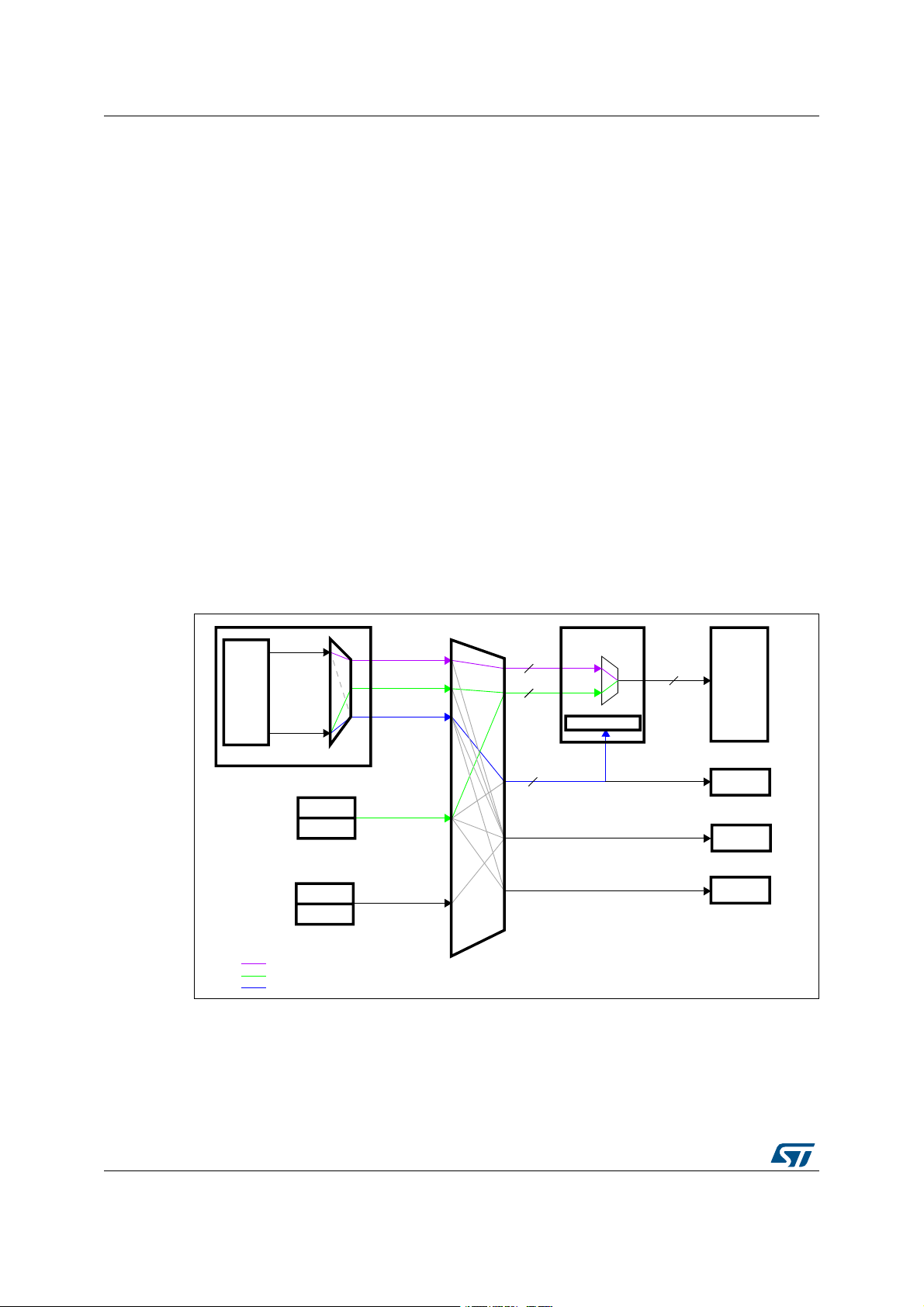
Figure 1 shows the Flash memory interface connection inside the system architecture.
Figure 1. Flash memory interface connection inside system architecture
!("
BIT
)#ODEBUS
#ORTEX
CORE
$CODEBUS
#ORTEX-
$-!
$-!
53"(3
%THERNET
!CCESSTOINSTRUCTIONSIN&LASHMEMORY
!CCESSTODATALITERALPOOLIN&LASHMEMORY
&,)4®ISTERACCESS
)#ODE
$#ODE
3BUS
INSTRUCTION
BIT
DATABUS
SYSTEM
BUS
!("
!("
BIT
BUS
&LASHINTERFACE
&,)4®ISTERS
&LASHMEMORY
BUS
BITS
&LASH
MEMORY
PERIPH
32!-S
&3-#
!("
PERIPH
AI
6/29 DocID15687 Rev 5
Page 7
PM0059 Flash memory interface
2.3 Flash memory
The Flash memory has the following main features:
• Capacity up to 1 Mbyte
• 128 bits wide data read
• Byte, half-word, word and double word write
• Sector and mass erase
• Memory organization
The Flash memory is organized as follows:
– Main memory block containing 4 sectors of 16 Kbytes, 1 sector of 64 Kbytes, and
7 sectors of 128 Kbytes
– System memory used to boot the device in System memory boot mode.
This area is reserved for STMicroelectronics and contains the bootloader which is
used to reprogram the Flash memory through one of the following interfaces:
USART1, USART3, CAN2, USB OTG FS in Device mode (DFU: device firmware
upgrade). The bootloader is programmed by ST when the device is manufactured,
and protected against spurious write/erase operations.
– 512 OTP (one-time programmable) bytes for user data
The OTP area contains 16 additional bytes used to lock the corresponding OTP
data block.
– Option bytes: read and write protections, BOR level, watchdog software/hardware
and reset when the device is in Standby or Stop mode.
• Low power modes (for details refer to the Power control (PWR) section of the reference
manual)
Table 2. Flash module organization
Block Name Block base addresses Size
Sector 0 0x0800 0000 - 0x0800 3FFF 16 Kbyte
Sector 1 0x0800 4000 - 0x0800 7FFF 16 Kbyte
Sector 2 0x0800 8000 - 0x0800 BFFF 16 Kbyte
Sector 3 0x0800 C000 - 0x0800 FFFF 16 Kbyte
Sector 4 0x0801 0000 - 0x0801 FFFF 64 Kbyte
Main memory
System memory 0x1FFF 0000 - 0x1FFF 77FF 30 Kbyte
OTP area 0x1FFF 7800 - 0x1FFF 7A0F 528 bytes
Option bytes 0x1FFF C000 - 0x1FFF C00F 16 bytes
Sector 5 0x0802 0000 - 0x0803 FFFF 128 Kbyte
Sector 6 0x0804 0000 - 0x0805 FFFF 128 Kbyte
.
.
.
Sector 11 0x080E 0000 - 0x080F FFFF 128 Kbyte
.
.
.
.
.
.
DocID15687 Rev 5 7/29
28
Page 8

Flash memory interface PM0059
2.4 Read interface
2.4.1 Relation between CPU clock frequency and Flash memory read time
To correctly read data from Flash memory, the number of wait states (LATENCY) must be
correctly programmed in the Flash access control register (FLASH_ACR) according to the
frequency of the CPU clock (HCLK) and the supply voltage of the device. Table 3 shows the
correspondence between wait states and CPU clock frequency.
The prefetch must be disabled when the supply voltage is below 2.1 V.
Table 3. Number of wait states according to CPU clock (HCLK) frequency
HCLK (MHz)
Wait st ate s (WS)
(LATENCY)
0 WS (1 CPU cycle) 0 <HCLK≤ 30 0 <HCLK ≤ 24 0 <HCLK ≤ 18 0 < HCLK ≤ 16
1 WS (2 CPU cycles) 30 <HCLK ≤ 60 24 < HCLK≤ 48 18 <HCLK ≤ 36 16 <HCLK ≤ 32
2 WS (3 CPU cycles) 60 <HCLK ≤ 90 48 < HCLK≤ 72 36 < HCLK≤ 54 32 < HCLK≤ 48
3 WS (4 CPU cycles) 90 <HCLK ≤ 120 72 < HCLK≤ 96 54 <HCLK ≤ 72 48 < HCLK≤ 64
4 WS (5 CPU cycles)
V oltage range
2.7 V - 3.6 V
Voltage range
2.4 V - 2.7 V
96 < HCLK≤ 120 72 < HCLK≤ 90 64 < HCLK≤ 80
Voltage range
2.1 V - 2.4 V
Voltage range
1.8 V - 2.1 V
(1)
5 WS (6 CPU cycles)
6 WS (7 CPU cycles)
7 WS (8 CPU cycles)
1. If IRROFF is set to VDD on STM32F20xx devices, this value can be lowered to 1.65 V when the device operates in a
reduced temperature range.
90 < HCLK≤ 108 80 < HCLK≤ 96
108 < HCLK≤ 120 96 < HCLK≤ 112
112 < HCLK≤ 120
After reset, the CPU clock frequency is 16 MHz and 0 wait state (WS) is configured in the
FLASH_ACR register.
It is highly recommended to use the following software sequences to tune the number of
wait states needed to access the Flash memory with the CPU frequency.
Increasing the CPU frequency
1. Program the new number of wait states to the LATENCY bits in the FLASH_ACR
register
2. Check that the new number of wait states is taken into account to access the Flash
memory by reading the FLASH_ACR register
3. Modify the CPU clock source by writing the SW bits in the RCC_CFGR register
4. If needed, modify the CPU clock prescaler by writing the HPRE bits in RCC_CFGR
5. Check that the new CPU clock source or/and the new CPU clock prescaler value is/are
taken into account by reading the clock source status (SWS bits) or/and the AHB
prescaler value (HPRE bits), respectively, in the RCC_CFGR register.
8/29 DocID15687 Rev 5
Page 9

PM0059 Flash memory interface
Decreasing the CPU frequency
1. Modify the CPU clock source by writing the SW bits in the RCC_CFGR register
2. If needed, modify the CPU clock prescaler by writing the HPRE bits in RCC_CFGR
3. Check that the new CPU clock source or/and the new CPU clock prescaler value is/are
taken into account by reading the clock source status (SWS bits) or/and the AHB
prescaler value (HPRE bits), respectively, in the RCC_CFGR register
4. Program the new number of wait states to the LATENCY bits in FLASH_ACR
5. Check that the new number of wait states is used to access the Flash memory by
reading the FLASH_ACR register
Note: A change in CPU clock configuration or wait state (WS) configuration may not be effective
straight away. To make sure that the current CPU clock frequency is the one you have
configured, you can check the AHB prescaler factor and clock source status values. To
make sure that the number of WS you have programmed is effective, you can read the
FLASH_ACR register.
2.4.2 Adaptive real-time memory accelerator (ART Accelerator™)
The proprietary Adaptive real-time (ART) memory accelerator is optimized for STM32
industry-standard ARM
®
Cortex™-M3 processors. It balances the inherent performance
advantage of the ARM Cortex-M3 over Flash memory technologies, which normally requires
the processor to wait for the Flash memory at higher operating frequencies.
To release the processor full performance of 150 DMIPS, the accelerator implements an
instruction prefetch queue and branch cache which increases program execution speed
from the 128-bit Flash memory. Based on CoreMark benchmark, the performance achieved
thanks to the ART accelerator is equivalent to 0 wait state program execution from Flash
memory at a CPU frequency up to 120 MHz.
Instruction prefetch
Each Flash memory read operation provides 128 bits from either four instructions of 32 bits
or 8 instructions of 16 bits according to the program launched. So, in case of sequential
code, at least four CPU cycles are needed to execute the previous read instruction line.
Prefetch on the I-Code bus can be used to read the next sequential instruction line from the
Flash memory while the current instruction line is being requested by the CPU. Prefetch is
enabled by setting the PRFTEN bit in the FLASH_ACR register. This feature is useful if at
least one wait state is needed to access the Flash memory.
Figure 2 shows the execution of sequential 32-bit instructions with and without prefetch
when 3 WSs are needed to access the Flash memory.
DocID15687 Rev 5 9/29
28
Page 10

Flash memory interface PM0059
AI
&
&
&
&
$
$
$
$
%
%
%
%
&
&
&
&
$
$
$
%
%
2EADINS 'IVESINS 2EADINS 'IVESINS
INS
FETCH
INS
FETCH
INS
FETCH
INS
FETCH
INS
FETCH
INS
FETCH
INS
FETCH
INS
FETCH
7!)4
7!)4
$%
&
&
&
&
$
$
$
%
%
&
&
&
&
$
$
$
%
%
7AITDATA
%
2EADINS 'IVESINS 'IVESINS
2EADINS 2EADINS
INS INS
FETCH
INS INS
7ITHOUTPREFETCH
7ITHPREFETCH
&$%
#ORTEX-PIPELINE
!("PROTOCOL
ADDRESSREQUESTED
&&ETCHSTAGE
$$ECODESTAGE
%%XECUTESTAGE
INS
FETCH
INS
FETCH
INS
FETCH FETCH FETCH FETCH
INS
FETCH
Figure 2. Sequential 32-bit instruction execution
When the code is not sequential (branch), the instruction may not be present in the currently
used instruction line or in the prefetched instruction line. In this case (miss), the penalty in
terms of number of cycles is at least equal to the number of wait states.
10/29 DocID15687 Rev 5
Page 11

PM0059 Flash memory interface
Instruction cache memory
To limit the time lost due to jumps, it is possible to retain 64 lines of 128 bits in an instruction
cache memory. This feature can be enabled by setting the instruction cache enable (ICEN)
bit in the FLASH_ACR register. Each time a miss occurs (requested data not present in the
currently used instruction line, in the prefetched instruction line or in the instruction cache
memory), the line read is copied into the instruction cache memory. If some data contained
in the instruction cache memory are requested by the CPU, they are provided without
inserting any delay. Once all the instruction cache memory lines have been filled, the LRU
(least recently used) policy is used to determine the line to replace in the instruction memory
cache. This feature is particularly useful in case of code containing loops.
Data management
Literal pools are fetched from Flash memory through the D-Code bus during the execution
stage of the CPU pipeline. The CPU pipeline is consequently stalled until the requested
literal pool is provided. To limit the time lost due to literal pools, accesses through the AHB
databus D-Code have priority over accesses through the AHB instruction bus I-Code.
If some literal pools are frequently used, the data cache memory can be enabled by setting
the data cache enable (DCEN) bit in the FLASH_ACR register. This feature works like the
instruction cache memory, but the retained data size is limited to 8 rows of 128 bits.
Note: Data in user configuration sector are not cacheable.
2.5 Erase and program operations
For any Flash memory program operation (erase or program), the CPU clock frequency
(HCLK) must be at least 1 MHz. The contents of the Flash memory are not guaranteed if a
device reset occurs during a Flash memory operation.
During a write/erase operation to the Flash memory, any attempt to read the Flash memory
will caused the bus to stall. Read operations are processed correctly once the program
operation has completed. This means that code or data fetches cannot be performed while
a write/erase operation is ongoing.
2.5.1 Unlocking the Flash control register
After reset, write is not allowed in the Flash control register (FLASH_CR) to protect the
Flash memory against possible unwanted operations due, for example, to electric
disturbances. The following sequence is used to unlock this register:
1. Write KEY1 = 0x45670123 in the Flash key register (FLASH_KEYR)
2. Write KEY2 = 0xCDEF89AB in the Flash key register (FLASH_KEYR)
Any wrong sequence will return a bus error and lock up the FLASH_CR register until the
next reset.
The FLASH_CR register can be locked again by software by setting the LOCK bit in the
FLASH_CR register.
Note: The FLASH_CR register is not accessible in write mode when the BSY bit in the FLASH_SR
register is set. Any attempt to write to it with the BSY bit set will cause the AHB bus to stall
until the BSY bit is cleared.
DocID15687 Rev 5 11/29
28
Page 12

Flash memory interface PM0059
2.5.2 Program/erase parallelism
The Parallelism size is configured through the PSIZE field in the FLASH_CR register. It
represents the number of bytes to be programmed each time a write operation occurs to the
Flash memory. PSIZE is limited by the supply voltage and by whether the external V
supply is used or not. It must therefore be correctly configured in the FLASH_CR register
before any programming/erasing operation.
A Flash memory erase operation can only be performed by sectors, bank or for the whole
Flash memory (mass erase). The erase time depends on PSIZE programmed value. For
more details on the erase time, refer to the electrical characteristics section of the device
datasheet.
V oltage range
2.7 - 3.6 V
with External
V
Parallelism
size
PSIZE(1:0) 11 10 01 00
x64 x32 x16 x8
Ta bl e 4. Progra m/e ras e parallelism
Voltage range
2.7 - 3.6 V
PP
Voltage range
2.4 - 2.7 V
V oltage range
2.1 - 2.4 V
Voltage range
1.8 V - 2.1 V
PP
(1)
1. If IRROFF is set to VDD on STM32F20xx devices, this value can be lowered to 1.65 V when the device
operates in a reduced temperature range.
Note: Any program or erase operation started with in consistent program p arallelism/volt age range
settings may lead to unpredicted results. Even if a subsequent read operation indicates th at
the logical value was effectively written to the memory, this value may not be retained.
T o use V
, an external high-voltage supply (between 8 and 9 V) must be applied to the VPP
PP
pad. The external supply must be able to sustain this voltage range even if the DC
consumption exceeds 10 mA. It is advised to limit the use of VPP to initial programming on
the factory line. The V
supply must not be applied for more than an hour, otherwise the
PP
Flash memory might be damaged.
2.5.3 Erase
The Flash memory erase operation can be performed at sector level or on the whole Flash
memory (Mass Erase). Mass Erase does not affect the OTP sector or the configuration
sector.
Sector Erase
To erase a sector, follow the procedure below:
1. Check that no Flash memory operation is ongoing by checking the BSY bit in the
FLASH_SR register
2. Set the SER bit and select the sector (out of the 12 sectors in the main memory block)
you wish to erase (SNB) in the FLASH_CR register
3. Set the STRT bit in the FLASH_CR register
4. Wait for the BSY bit to be cleared
12/29 DocID15687 Rev 5
Page 13

PM0059 Flash memory interface
Mass Erase
To perform Mass Erase, the following sequence is recommended:
1. Check that no Flash memory operation is ongoing by checking the BSY bit in the
FLASH_SR register
2. Set the MER bit in the FLASH_CR register
3. Set the STRT bit in the FLASH_CR register
4. Wait for the BSY bit to be cleared
2.5.4 Programming
Standard programming
The Flash memory programming sequence is as follows:
1. Check that no main Flash memory operation is ongoing by checking the BSY bit in the
FLASH_SR register.
2. Set the PG bit in the FLASH_CR register
3. Perform the data write operation(s) to the desired memory address (inside main
memory block or OTP area):
– Byte access in case of x8 parallelism
– Half-word access in case of x16 parallelism
– Word access in case of x32 parallelism
– Double word access in case of x64 parallelism
4. Wait for the BSY bit to be cleared
Note: Successive write operations are possible without the need of an erase operation when
changing bits from ‘1’ to ‘0’.
Writing ‘1’ requires a Flash memory erase operation.
If an erase and a program operation are requested simultane ously, the erase operation is
performed first.
Programming errors
It is not allowed to program data to the Flash memory that would cross the 128-bit row
boundary. In such a case, the write operation is not performed and a program alignment
error flag (PGAERR) is set in the FLASH_SR register.
The write access type (byte, half-word, word or double word) must correspond to the type of
parallelism chosen (x8, x16, x32 or x64). If not, the write operation is not performed and a
program parallelism error flag (PGPERR) is set in the FLASH_SR register.
If the standard programming sequence is not respected (for example, if there is an attempt
to write to a Flash memory address when the PG bit is not set), the operation is aborted and
a program sequence error flag (PGSERR) is set in the FLASH_SR register.
Programming and caches
If a Flash memory write access concerns some data in the data cache, the Flash write
access modifies the data in the Flash memory and the data in the cache.
If an erase operation in Flash memory also concerns data in the data or instruction cache,
you have to make sure that these data are rewritten before they are accessed during code
DocID15687 Rev 5 13/29
28
Page 14

Flash memory interface PM0059
execution. If this cannot be done safely, it is recommended to flush the caches by setting the
DCRST and ICRST bits in the FLASH_CR register.
Note: The I/D cache should be flushed only when it is disabled (I/DCEN = 0).
2.5.5 Interrupts
Setting the end of operation interrupt enable bit (EOPIE) in the FLASH_CR register enables
interrupt generation when an erase or program operation ends, that is when the busy bit
(BSY) in the FLASH_SR register is cleared (operation completed, correctly or not). In this
case, the end of operation (EOP) bit in the FLASH_SR register is set.
If an error occurs during a program or erase operation request, one of the following error
flags is set in the FLASH_SR register:
• PGAERR, PGPERR, PGSERR (Program error flags)
• WRPERR (Protection error flag)
In this case, if the error interrupt enable bit (ERRIE) is set in the FLASH_SR register, an
interrupt is generated and the operation error bit (OPERR) is set in the FLASH_SR register.
Note: If several successive errors are detected (for example, in case of DMA transfer to the Flash
memory), the error flags cannot be cleared until the end of the successive write requests.
Refer to Table 5: Flash interrupt requests for summary of Flash interrupt request.
Table 5. Flash interrupt requests
Interrupt events Event flags Enable control bits
End of operation EOP EOPIE
Write protection error WRPERR ERRIE
Programming error PGAERR, PGPERR, PGSERR ERRIE
2.6 Option bytes
2.6.1 Description of user option bytes
The option bytes are configured by the end user depending on the application requirements.
Table 6 shows the organization of these bytes inside the user configuration sector.
Address [63:16] [15:0]
0x1FFF C000 Reserved ROP & user option bytes (RDP & USER)
0x1FFF C008 Reserved Write protections nWRP
Table 6. Option byte organization
14/29 DocID15687 Rev 5
Page 15

PM0059 Flash memory interface
RDP: Read protection option byte.
The read protection is used to protect the software code stored in Flash memory.
0xAA: Level 0, no protection
Bits 15:8
USER: User option byte
This byte is used to configure the following features:
– Select the watchdog event: Hardware or software
– Reset event when entering the Stop mode
– Reset event when entering the Standby mode
Bit 7
Bit 6
Bit 5
Bit 4 0x1: Not used
Bits 3:2
Bits 1:0 0x1: Not used
0xCC: Level 2, chip protection (debug and boot from RAM features disabled)
Others: Level 1, read protection of memories (debug features limited)
nRST_STDBY
nRST_STOP
WDG_SW
BOR_LEV: BOR reset Level
Table 7. Description of the option bytes
Option bytes (word, address 0x1FFF C000)
0: Reset generated when entering the Standby mode
1: No reset generated
0: Reset generated when entering the Stop mode
1: No reset generated
0: Hardware watchdog
1: Software watchdog
These bits contain the supply level threshold that activates/releases the reset.
They can be written to program a new BOR level value into Flash memory.
00: BOR Level 3 (VBOR3). reset threshold level from 2.70 to 3.60 V
01: BOR Level 2 (VBOR2). reset threshold level from 2.40 to 2.70 V
10: BOR Level 1 (VBOR1). reset threshold level from 2.10 to 2.40 V
11: BOR off (VBOR0), reset threshold level from 1.8 to 2.10 V
Option bytes (word, address 0x1FFF C008)
Bits 15:12 0xF: Not used
nWRP: Flash memory write protection option bytes
Sectors 0 to 11 can be write protected.
Bit i
(0 ≤ i ≤ 11)
nWRPi
0: Write protection active on sector i
1: Write protection not active on sector i
2.6.2 Programming user option bytes
To run any operation on this sector, the option lock bit (OPTLOCK) in the Flash option
control register (FLASH_OPTCR) must be cleared. To be allowed to clear this bit, you have
to perform the following sequence:
1. Write OPTKEY1 = 0x0819 2A3B in the Flash option key register (FLASH_OPTKEYR)
2. Write OPTKEY2 = 0x4C5D 6E7F in the Flash option key register (FLASH_OPTKEYR)
DocID15687 Rev 5 15/29
28
Page 16

Flash memory interface PM0059
The user option bytes can be protected against unwanted erase/program operations by
setting the OPTLOCK bit by software.
Modifying user option bytes
To modify the user option value, follow the sequence below:
1. Check that no Flash memory operation is ongoing by checking the BSY bit in the
FLASH_SR register
2. Write the desired option value in the FLASH_OPTCR register
3. Set the option start bit (OPTSTRT) in the FLASH_OPTCR register
4. Wait for the BSY bit to be cleared
Note: The value of an option is automatically modified by first erasing the user configuration sector
and then programming all the option by tes wi th the value s cont ained in the FLASH_OPTCR
register.
2.6.3 Read protection (RDP)
The user area in the Flash memory can be protected against read operations by an
entrusted code. Three read protection levels are defined:
• Level 0: no read protection
When the read protection level is set to Level 0 by writing 0xAA into the read protection
option byte (RDP), all read/write operations (if no write protection is set) from/to the
Flash memory or the backup SRAM are possible in all boot configurations (Flash user
boot, debug or boot from RAM).
• Level 1: memory read protection.
It is the default read protection level after option byte erase. The read protection Level
1 is activated by writing any value (except for 0xAA and 0xCC used to set Level 0 and
Level 2, respectively) into the RDP option byte. When the read protection Level 1 is set:
– No access (read, erase, program) to Flash memory or backup SRAM can be
performed while the debug feature is connected or while booting from RAM or
system memory bootloader. A bus error is generated in case of read request.
– When booting from Flash memory, accesses (read, erase, program) to Flash
memory and backup SRAM from user code are allowed.
When Level 1 is active, programming the protection option byte (RDP) to Level 0
causes the Flash memory and the backup SRAM to be mass-erased. As a result the
user code area is cleared before the read protection is removed. The mass erase only
erases the user code area. The other option bytes including write protections remain
16/29 DocID15687 Rev 5
Page 17

PM0059 Flash memory interface
unchanged from before the mass-erase operation. The OTP area is not affected by
mass erase and remains unchanged.
Mass erase is performed only when Level 1 is active and Level 0 requested. When the
protection level is increased (0->1, 1->2, 0->2) there is no mass erase.
• Level 2: Disable debug/chip read protection
When the read protection Level 2 is set by writing 0xCC to the RDP option byte:
– All protections provided by Level 1 are active.
– Booting from system memory is not allowed anymore.
– JTAG, SWV (single-wire viewer) are disabled.
– User option bytes can no longer be changed.
– When booting from Flash memory, accesses (read, erase and program) to Flash
memory and backup SRAM from user code are allowed.
Memory read protection Level 2 is an irreversible operation. When Level 2 is activated,
the level of protection cannot be decreased to Level 0 or Level 1.
Note: The JTAG por t is permanently disable d when Level 2 is active ( acting as a JTAG fuse). As a
consequence, boundary scan cannot be performed. STMicroelectronics is not able to
perform analysis on defective parts on which the Level 2 protection has been set.
Figure 3 shows how to go from one RDP level to another, and Table 8 summarizes the
memory accesses versus the protection level.
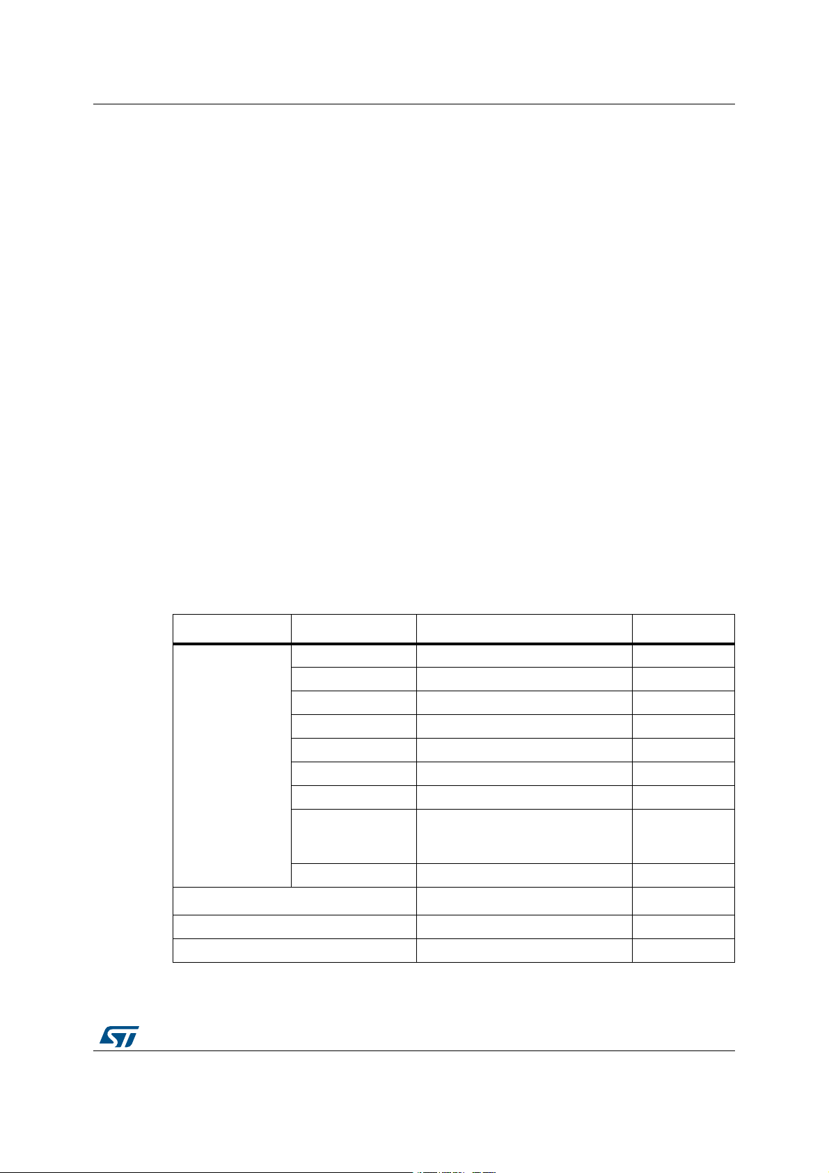
Table 8. Access versus read protection level
Debug features, Boot from RAM or
Memory area
Main Flash Memory
and Backup SRAM
Option Bytes
OTP
1. The main Flash memory and backup SRAM are only erased when the RDP changes from level 1 to 0. The OTP area
remains unchanged.
Protection
Level
Level 1 NO NO
Level 2 NO YES
Level 1 YES YES
Level 2 NO NO
Level 1 NO NA YES NA
Level 2 NO NA YES NA
from System memory bootloader
Read Write Erase Read Write Erase
(1)
Booting from Flash memory
YES
DocID15687 Rev 5 17/29
28
Page 18

Flash memory interface PM0059
,EVEL
LEVE,LEVE,
H!!0$2H##0$2
2$0!!H
2$0##H
DEFAULT
/PTIONSWRITE2$0LEVELINCREASEINCLUDES
/PTIONSERASE
.EWOPTIONSPROGRAM
/PTIONSWRITE2$0LEVELDECREASEINCLUDES
-ASSERASE
/PTIONSERASE
.EWOPTIONSPROGRAM
/PTIONSWRITE2$0LEVELIDENTICALINCLUDES
/PTIONSERASE
.EWOPTIONSPROGRAM
2$0!!H
/THERSOPTIONSMODIFIED
2$0!!H##H
/THERSOPTIONSMODIFIED
7RITEOPTIONS
INCLUDING
2$0!!H
7RITEOPTIONS
INCLUDING
2$0##H
7RITEOPTIONS
INCLUDING
2$0##H
7RITEOPTIONSINCLUDING
2$0##H!!H
AI
Figure 3. RDP levels
2.6.4 Write protections
The user sectors (0 to 11) in Flash memory can be protected against unwanted write
operations due to loss of program counter contexts. When the not write protection bit in
sector i (nWRPi, 0 ≤ i ≤ 11) is low, the corresponding sector cannot be erased or
programmed. Consequently, a mass erase cannot be performed if one of the sectors is
write-protected.
If an erase/program operation to a write-protected part of the Flash memory is attempted
(sector protected by write protection bit, OTP part locked or part of the Flash memory that
can never be written like the ICP), the write protection error flag (WRPERR) is set in the
FLASH_SR register.
Note: When the memory read protection level is selected (RDP level = 1), it is not possible to
program or erase Flash memory sector i if the CPU debug features are co nnected ( JTAG or
single wire) or boot code is being executed from RAM, even if nWRPi = 1.
18/29 DocID15687 Rev 5
Page 19

PM0059 Flash memory interface
Write protection error flag
If an erase/program operation to a write protected area of the Flash memory is performed,
the Write Protection Error flag (WRPERR) is set in the FLASH_SR register.
If an erase operation is requested, the WRPERR bit is set when:
• Mass or sector erase are configured (MER or MER/MER1 and SER = 1)
• A sector erase is requested and the Sector Number SNB field is not valid
• A mass erase is requested while at least one of the user sector is write protected by
option bit (MER or MER/MER1 = 1 and nWRPi = 0 with 0 ≤ i ≤ 11 bits in the
FLASH_OPTCRx register
• The Flash memory is readout protected and an intrusion is detected.
If a program operation is requested, the WRPERR bit is set when:
• A write operation is performed on system memory or on the reserved part of the user
specific sector.
• A write operation is performed to the user configuration sector
• A write operation is performed on a sector write protected by option bit.
• A write operation is requested on an OTP area which is already locked
• The Flash memory is read protected and an intrusion is detected.
2.7 One-time programmable bytes
Table 9 shows the organization of the one-time programmable (OTP) part of the OTP area.
Block [128:96] [95:64] [63:32] [31:0] Address byte 0
0
1
.
.
.
15
Lock block
OTP0 OTP0 OTP0 OTP0 0x1FFF 7800
OTP0 OTP0 OTP0 OTP0 0x1FFF 7810
OTP1 OTP1 OTP1 OTP1 0x1FFF 7820
OTP1 OTP1 OTP1 OTP1 0x1FFF 7830
OTP15 OTP15 OTP15 OTP15 0x1FFF 79E0
OTP15 OTP15 OTP15 OTP15 0x1FFF 79F0
LOCKB15 ...
LOCKB12
The OTP area is divided into 16 OTP data blocks of 32 bytes and one lock OTP block of 16
bytes. The OTP data and lock blocks cannot be erased. The lock block contains 16 bytes
LOCKBi (0 ≤ i ≤ 15) to lock the corresponding OTP data block (blocks 0 to 15). Each OTP
data block can be programmed until the value 0x00 is programmed in the corresponding
OTP lock byte. The lock bytes must only contain 0x00 and 0xFF values, otherwise the OTP
bytes might not be taken into account correctly.
Table 9. OTP part organization
.
.
.
LOCKB11 ...
LOCKB8
LOCKB7 ...
LOCKB4
LOCKB3 ...
LOCKB0
.
.
.
0x1FFF 7A00
DocID15687 Rev 5 19/29
28
Page 20

Flash memory interface PM0059
2.8 Flash interface registers
2.8.1 Flash access control register (FLASH_ACR)
The Flash access control register is used to enable/disable the acceleration features and
control the Flash memory access time according to CPU frequency.
Address offset: 0x00
Reset value: 0x0000 0000
Access: no wait state, word, half-word and byte access
31 30 29 28 27 26 25 24 23 22 21 20 19 18 17 16
15 14 13 12 11 10 9 8 7 6 5 4 3 2 1 0
Reserved
DCRST ICRST DCEN ICEN PRFTEN
rwwrwrw rw rwrwrw
Bits 31:11 Reserved, must be kept cleared.
Bit 12 DCRST: Data cache reset
0: Data cache is not reset
1: Data cache is reset
This bit can be written only when the D cache is disabled.
Bit 11 ICRST: Instruction cache reset
0: Instruction cache is not reset
1: Instruction cache is reset
This bit can be written only when the I cache is disabled.
Bit 10 DCEN: Data cache enable
0: Data cache is disabled
1: Data cache is enabled
Reserved
Reserved
LATENCY
Bit 9 ICEN: Instruction cache enable
0: Instruction cache is disabled
1: Instruction cache is enabled
Bit 8 PRFTEN: Prefetch enable
0: Prefetch is disabled
1: Prefetch is enabled
Bits 7:3 Reserved, must be kept cleared.
Bits 2:0 LATENCY: Latency
These bits represent the ratio of the CPU clock period to the Flash memory access time.
000: Zero wait state
001: One wait state
010: Two wait states
011: Three wait states
100: Four wait states
101: Five wait states
110: Six wait states
111: Seven wait states
20/29 DocID15687 Rev 5
Page 21

PM0059 Flash memory interface
2.8.2 Flash key register (FLASH_KEYR)
The Flash key register is used to allow access to the Flash control register and so, to allow
program and erase operations.
Address offset: 0x04
Reset value: 0x0000 0000
Access: no wait state, word access
31 30 29 28 27 26 25 24 23 22 21 20 19 18 17 16
wwwwww w w w w w w w w w w
1514131211109876543210
wwwwww w w w w w w w w w w
KEY[31:16]
KEY[15:0]
Bits 31:0 FKEYR: FPEC key
The following values must be programmed consecutively to unlock the FLASH_CR register
and allow programming/erasing it:
a) KEY1 = 0x45670123
b) KEY2 = 0xCDEF89AB
2.8.3 Flash option key register (FLASH_OPTKEYR)
The Flash option key register is used to allow program and erase operations in the user
configuration sector.
Address offset: 0x08
Reset value: 0x0000 0000
Access: no wait state, word access
31 30 29 28 27 26 25 24 23 22 21 20 19 18 17 16
wwwwww w w w w w ww w w w
15 14 13 12 11 10 9 8 7 6 5 4 3 2 1 0
wwwwww w w w w w ww w w w
OPTKEYR[31:16
OPTKEYR[15:0]
Bits 31:0 OPTKEYR: Option byte key
The following values must be programmed consecutively to unlock the FLASH_OPTCR
register and allow programming it:
a) OPTKEY1 = 0x08192A3B
b) OPTKEY2 = 0x4C5D6E7F
DocID15687 Rev 5 21/29
28
Page 22

Flash memory interface PM0059
2.8.4 Flash status register (FLASH_SR)
The Flash status register gives information on ongoing program and erase operations.
Address offset: 0x0C
Reset value: 0x0000 0000
Access: no wait state, word, half-word and byte access
31 30 29 28 27 26 25 24 23 22 21 20 19 18 17 16
15 14 13 12 11 10 9 8 7 6 5 4 3 2 1 0
Reserved
Reserved
Bits 31:17 Reserved, must be kept cleared.
Bit 16 BSY: Busy
This bit indicates that a Flash memory operation is in progress. It is set at the beginning of a
Flash memory operation and cleared when the operation finishes or an error occurs.
0: no Flash memory operation ongoing
1: Flash memory operation ongoing
PGSERR PGPERR PGAERR WRPERR
rc_w1 rc_w1 rc_w1 rc_w1 rc_w1 rc_w1
Reserved
OPERR EOP
BSY
r
Bits 15:8 Reserved, must be kept cleared.
Bit 7 PGSERR: Programming sequence error
Set by hardware when a write access to the Flash memory is performed by the code while
the control register has not been correctly configured.
Cleared by writing 1.
Bit 6 PGPERR: Programming parallelism error
Set by hardware when the size of the access (byte, half-word, word, double word) during the
program sequence does not correspond to the parallelism configuration PSIZE (x8, x16,
x32, x64).
Cleared by writing 1.
Bit 5 PGAERR: Programming alignment error
Set by hardware when the data to program cannot be contained in the same 128-bit Flash
memory row.
Cleared by writing 1.
Bit 4 WRPERR: Write protection error
Set by hardware when an address to be erased/programmed belongs to a write-protected
part of the Flash memory.
Cleared by writing 1.
22/29 DocID15687 Rev 5
Page 23

PM0059 Flash memory interface
Bits 3:2 Reserved, must be kept cleared.
Bit 1 OPERR: Operation error
Set by hardware when a flash operation (programming / erase) request is detected and can
not be run because of parallelism, alignment, sequence or write protection error. This bit is
set only if error interrupts are enabled (ERRIE = 1).
Bit 0 EOP: End of operation
Set by hardware when one or more Flash memory operations (program/erase) has/have
completed successfully. It is set only if the end of operation interrupts are enabled (EOPIE =
1).
Cleared by writing a 1.
2.8.5 Flash control register (FLASH_CR)
The Flash control register is used to configure and start Flash memory operations.
Address offset: 0x10
Reset value: 0x8000 0000
Access: no wait state when no Flash memory operation is ongoing, word, half-word and
byte access.
31 30 29 28 27 26 25 24 23 22 21 20 19 18 17 16
LOCK
rs rw rw rs
15 14 13 12 11 10 9 8 7 6 5 4 3 2 1 0
Reserved
Reserved
ERRIE EOPIE
PSIZE[1:0]
rw rw rw rw rw rw rw rw rw
Bit 31 LOCK: Lock
Write to 1 only. When it is set, this bit indicates that the FLASH_CR register is locked. It is
cleared by hardware after detecting the unlock sequence.
In the event of an unsuccessful unlock operation, this bit remains set until the next reset.
Bits 31:26 Reserved, must be kept cleared.
Bit 25 ERRIE: Error interrupt enable
This bit enables the interrupt generation when the OPERR bit in the FLASH_SR register is
set to 1.
0: Error interrupt generation disabled
1: Error interrupt generation enabled
Bit 24 EOPIE: End of operation interrupt enable
This bit enables the interrupt generation when the EOP bit in the FLASH_SR register goes
to 1.
0: Interrupt generation disabled
1: Interrupt generation enabled
Bits 23:17 Reserved, must be kept cleared.
Bit 16 STRT: Start
This bit triggers an erase operation when set. It is set only by software and cleared when the
BSY bit is cleared.
Reserv
ed
Reserved
SNB[3:0] MER SER PG
STRT
Bits 15:10 Reserved, must be kept cleared.
DocID15687 Rev 5 23/29
28
Page 24

Flash memory interface PM0059
Bits 9:8 PSIZE: Program size
These bits select the program parallelism.
00 program x8
01 program x16
10 program x32
11 program x64
Bit 7 Reserved, must be kept cleared.
Bits 6:3 SNB: Sector number
These bits select the sector to erase.
0000 sector 0
0001 sector 1
...
1011 sector 11
Others not allowed
Bit 2 MER: Mass Erase
Erase activated for all user sectors.
Bit 1 SER: Sector Erase
Sector Erase activated.
Bit 0 PG: Programming
Flash programming activated.
2.8.6 Flash option control register (FLASH_OPTCR)
The FLASH_OPTCR register is used to modify the user option bytes.
Address offset: 0x14
Reset value: 0x0FFF AAED. The option bits are loaded with values from Flash memory at
reset release.
Access: no wait state when no Flash memory operation is ongoing, word, half-word and
byte access.
31 30 29 28 27 26 25 24 23 22 21 20 19 18 17 16
1514131211109876543210
rw rw rw rw rw rw rw rw rw rw rw rw rw rs rs
Reserved
nWRP[11:0]
rw rw rw rw rw rw rw rw rw rw rw rw
nRST_
RDP[7:0]
STDBY
nRST_
STOP
WDG_
SW
Reserv
ed
BOR_LEV
OPTSTRTOPTLO
CK
24/29 DocID15687 Rev 5
Page 25

PM0059 Flash memory interface
Bits 31:28 Reserved, must be kept cleared.
Bits 27:16 nWRP: Not write protect
These bits contain the value of the write-protection option bytes after reset. They can be
written to program a new write protect value into Flash memory.
0: Write protection active
1: Write protection not active
Bits 15:8 RDP: Read protect
These bits contain the value of the read-protection option level after reset. They can be
written to program a new read protection value into Flash memory.
0xAA: Level 0, read protection not active
0xCC: Level 2, chip read protection active
Others: Level 1, read protection of memories active
Bits 7:5 USER: User option bytes
These bits contain the value of the user option byte after reset. They can be written to
program a new user option byte value into Flash memory.
Bit 7: nRST_STDBY
Bit 6: nRST_STOP
Bit 5: WDG_SW
Note: When changing the WDG mode from hardware to software or from software to
hardware, a system reset is required to make the change effective.
Bit 4 Reserved, must be kept cleared.
Bits 3:2 BOR_LEV: BOR reset Level
These bits contain the supply level threshold that activates/releases the reset. They can be
written to program a new BOR level. By default, BOR is off. When the supply voltage (V
drops below the selected BOR level, a device reset is generated.
00: BOR Level 3 (VBOR3), reset threshold level 3
01: BOR Level 2 (VBOR2), reset threshold level 2
10: BOR Level 1 (VBOR1), reset threshold level 1
11: BOR off (VBOR0), POR/PDR reset threshold level is applied.
Note: For full details about BOR characteristics, refer to the “Electrical characteristics” section
in the device datasheet.
Bit 1 OPTSTRT: Option start
This bit triggers a user option operation when set. It is set only by software and cleared when
the BSY bit is cleared.
Bit 0 OPTLOCK: Option lock
Write to 1 only. When this bit is set, it indicates that the FLASH_OPTCR register is locked.
This bit is cleared by hardware after detecting the unlock sequence.
In the event of an unsuccessful unlock operation, this bit remains set until the next reset.
DD
)
DocID15687 Rev 5 25/29
28
Page 26

Flash memory interface PM0059
2.8.7 Flash interface register map
Offset Register
0x00
0x04
0x08
0x0C
0x10
FLASH_ACR
Reset value 00000 00 0
FLASH_KEY
R
Reset value 00000000000000000000000000000000
FLASH_OPT
KEYR
Reset value 00000000000000000000000000000000
FLASH_SR
Reset value 0 0000 0 0
FLASH_CR
Reset value 1 0 0 00 0000 00
Table 10. Flash register map and reset values
31302928272625242322212019181716151413
Reserved
KEY[31:16] KEY[15:0]
OPTKEYR[31:16] OPTKEYR[15:0]
Reserved
LOCK
Reserved
Reserved
EOPIE
BSY
STRT
Reserved
121110
DCRST
Reserved
987654321
ICEN
DCEN
ICRST
PSIZ
E[1:0
Reserved
PRFTEN
PGSERR
PGPERR
]
SNB[3:0]
Reserved
0
LATENC
Y
Rese
rved
PGAERR
WRPERR
MER
OPERR
SER
EOP
PG
0x14
FLASH_OPT
CR
Reset value 11111111111110101010111 110 1
Reserved
nWRP[11:0] RDP[7:0]
WDG_SW
nRST_STOP
nRST_STDBY
BOR_LEV
Reserved
OPTSTRT
OPTLOCK
26/29 DocID15687 Rev 5
Page 27

PM0059 Revision history
3 Revision history
Table 11. Document revision history
Date Revision Changes
Updated memory organization in Section 2.3: Flash memory, and
replace user-specific block by OTP area.
Updated addresses in Table 6: Option byte organization.
Definition of BOR_LEV[3:2] bits updated in Table 7: Description of
the option bytes and Section 2.8.6: Flash option control register
24-Jun-2010 1
(FLASH_OPTCR). Modified FLASH_OPTCR reset value in
Section 2.8.6: Flash option control register (FLASH_OPTCR) and
Table 10: Flash register map and reset values. Updated
OPTLOCK
definition.
Updated definition of ERRIE bit in Section 2.8.5: Flash control
register (FLASH_CR).
Updated size of OTP area, and option byte base address and size
in
Table 2: Flash module organization.
Changed 1.62 to 2.1 V range to 1.8 to 2.1 V, added Note 1 as well
as
wait states 4 to 7 in TTable 3: Number of wait states according to
CPU clock (HCLK) frequency.
Updated Table 4: Program/erase parallelism.
Updated BOR_LEVEL description in Table 7: Description of the
option bytes.
Renamed FLASH_FOCR, FLASH_OPTCR in Section 2.6.2:
Programming user option bytes.
09-Dec-2010 2
Updated Level 1 and Level 2 descriptions in Section 2.6.3: Read
protection (RDP).
Updated LATENCY bits in Section 2.8.1: Flash access control
register (FLASH_ACR) to support up to 7 wait states.
Changed access type to bits 0 to 7 to rc-1, and OPERR
description
in Section 2.8.4: Flash status register (FLASH_SR).
Changed access type to bits 16 and 31 to rs in Section 2.8.5:
Flash control register (FLASH_CR).
Changed access type to bits 0 and 1 to rs, and added note related
to
bit 7 to 5 in Section 2.8.6: Flash option control register
(FLASH_OPTCR).
30-Mar-2011 3
Updated OTP area in Section 2.3: Flash memory.
Updated Section 2.5: Erase and program operations to mention
the
fact that read operations cannot be performed during write/erase
operations.
DocID15687 Rev 5 27/29
28
Page 28

Revision history PM0059
Table 11. Document revision history (continued)
Date Revision Changes
Modified Note 1 in Table 3: Number of wait states according to
10-May-2011 4
07-Jun-2013 5
CPU clock (HCLK) frequency and Note 1 in Table 3: Number of
wait states according to CPU clock (HCLK) frequency.
Updated Section 2.4.1: Relation between CPU clock frequency
and Flash memory read time to add prefetch disabling when the
supply voltage is below 2.1 V.
Added note in Section : Standard programming
Updated Section 2.5.2: Program/erase parallelism.
Added Ta ble 5: Flash interrupt requests.
Updated Section 2.6.3: Read protection (RDP).
Updated Section 2.6.4: Write protections.
Modified BOR_LEV bits definition in Section 2.8.6: Flash option
control register (FLASH_OPTCR).
Document converted to new template and disclaimer updated.
28/29 DocID15687 Rev 5
Page 29

Please Read Carefully:
Information in this document is provided solely in connection with ST products. STMicroelectronics NV and its subsidiaries (“ST”) reserve the
right to make changes, corrections, modifications or improvements, to this document, and the products and services described herein at any
time, without notice.
All ST products are sold pursuant to ST’s terms and conditions of sale.
Purchasers are solely responsible for the choice, selection and use of the ST products and services described herein, and ST assumes no
liability whatsoever relating to the choice, selection or use of the ST products and services described herein.
No license, express or implied, by estoppel or otherwise, to any intellectual property rights is granted under this document. If any part of this
document refers to any third party products or services it shall not be deemed a license grant by ST for the use of such third party products
or services, or any intellectual property contained therein or considered as a warranty covering the use in any manner whatsoever of such
third party products or services or any intellectual property contained therein.
UNLESS OTHERWISE SET FORTH IN ST’S TERMS AND CONDITIONS OF SALE ST DISCLAIMS ANY EXPRESS OR IMPLIED
WARRANTY WITH RESPECT TO THE USE AND/OR SALE OF ST PRODUCTS INCLUDING WITHOUT LIMITATION IMPLIED
WARRANTIES OF MERCHANTABILITY, FITNESS FOR A PARTICUL AR PURPOS E (AND THEIR E QUIVALENTS UNDER THE LAWS
OF ANY JURISDICTION), OR INFRINGEMENT OF ANY PATENT, COPYRIGHT OR OTHER INTELLECTUAL PROPERTY RIGHT.
ST PRODUCTS ARE NOT AUTHORIZED FOR USE IN WEAPONS. NOR ARE ST PRODUCTS DESIGNED OR AUTHORIZED FOR USE
IN: (A) SAFETY CRITICAL APPLICATIONS SUCH AS LIFE SUPPORTING, ACTIVE IMPLANTED DEVICES OR SYSTEMS WITH
PRODUCT FUNCTIONAL SAFETY REQUIREMENTS; (B) AERONAUTIC APPLICATIONS; (C) AUTOMOTIVE APPLICATIONS OR
ENVIRONMENTS, AND/OR (D) AEROSPACE APPLICATIONS OR ENV IRONMENTS. WHERE ST PRODUCTS ARE NOT DESIGNED
FOR SUCH USE, THE PURCHASER SHALL USE PRODUCTS AT PURCHASER’S SOLE RISK, EVEN IF ST HAS BEEN INFORMED IN
WRITING OF SUCH USAGE, UNLESS A PRODUCT IS EXPRESSLY DESIGNATED BY ST AS BEING INTENDED FOR “AUTOMOTIVE,
AUTOMOTIVE SAFETY OR MEDICAL” INDUSTRY DOMAINS ACCORDING TO ST PRODUCT DESIGN SPECIFICATIONS.
PRODUCTS FORMALLY ESCC, QML OR JAN QUALIFIED ARE DEEMED SUITABLE FOR USE IN AEROSPACE BY THE
CORRESPONDING GOVERNMENTAL AGENCY.
Resale of ST products with provisions different from the statements and/or technical features set forth in this document shall immediately void
any warranty granted by ST for the ST product or service described herein and shall not create or extend in any manner whatsoever, any
liability of ST.
ST and the ST logo are trademarks or registered trademarks of ST in various countries.
Information in this document supersedes and replaces all information previously supplied.
The ST logo is a registered trademark of STMicroelectronics. All other names are the property of their respective owners.
© 2013 STMicroelectronics - All rights reserved
STMicroelectronics group of companies
Australia - Belgium - Brazil - Canada - China - Czech Republic - Finland - France - Germany - Hong Kong - India - Israel - Italy - Japan -
Malaysia - Malta - Morocco - Philippines - Singapore - Spain - Sweden - Switzerland - United Kingdom - United States of America
www.st.com
DocID15687 Rev 5 29/29
29
 Loading...