

STMicroelectronics STM32F050G6, STM32F050F6, STM32F050F4, STM32F050G4, STM32F050K4 User Manual
...Page 1
STM32F050x4 STM32F050x6
LQFP48 7x7 UFQFPN32 5x5
TSSOP20
UFQFPN28 4x4LQFP32 7x7
Low- and medium-density advanced ARM™-based 32-bit MCU with
up to 32 Kbytes Flash, timers, ADC and comm. interfaces
Datasheet production data
Features
■ Core: ARM 32-bit Cortex™-M0 CPU,
frequency up to 48 MHz
■ Memories
– 16 to 32 Kbytes of Flash memory
– 4 Kbytes of SRAM with HW parity checking
■ CRC calculation unit
■ Reset and supply management
– Voltage range: 2.0 V to 3.6 V
– Power-on/Power-down reset (POR/PDR)
– Programmable voltage detector (PVD)
– Low power modes: Sleep, Stop and
Standby
–V
■ Clock management
supply for RTC and backup registers
BAT
– 4 to 32 MHz crystal oscillator
– 32 kHz oscillator for RTC with calibration
– Internal 8 MHz RC with x6 PLL option
– Internal 40 kHz RC oscillator
■ Up to 39 fast I/Os
– All mappable on external interrupt vectors
– Up to 25 I/Os with 5 V tolerant capability
■ 5-channel DMA controller
■ 1 × 12-bit, 1.0 µs ADC (up to 10 channels)
– Conversion range: 0 to 3.6V
– Separate analog supply from 2.4 up to
3.6 V
■ Up to 9 timers
– 1 x 16-bit 7-channel advanced-control timer
for 6 channels PWM output, with deadtime
generation and emergency stop
– 1 x 32-bit and 1 x 16-bit timer, with up to 4
IC/OC, usable for IR control decoding
– 1 x 16-bit timer, with 2 IC/OC, 1 OCN,
deadtime generation and emergency stop
– 1 x 16-bit timer, with IC/OC and OCN,
deadtime generation, emergency stop and
modulator gate for IR control
– 1 x 16-bit timer with 1 IC/OC
– Independent and system watchdog timers
– SysTick timer: 24-bit downcounter
■ Calendar RTC with alarm and periodic wakeup
from Stop/Standby
■ Communication interfaces
– 1 x I
2
C interface; supporting Fast Mode
Plus (1 Mbit/s) with 20 mA current sink,
SMBus/PMBus, and wakeup from STOP
– 1 x USART supporting master synchronous
SPI and modem control; one with ISO7816
interface, LIN, IrDA capability auto baud
rate detection and wakeup feature
– 1 x SPI (18 Mbit/s) with 4 to 16
programmable bit frame, with I
2
S interface
multiplexed
■ Serial wire debug (SWD)
■ 96-bit unique ID
Table 1. Device summary
Reference Part number
STM32F050x4
STM32F050x6
STM32F050F4, STM32F050G4, STM32F050K4,
STM32F050C4
STM32F050F6, STM32F050G6, STM32F050K6,
STM32F050C6
September 2012 Doc ID 023079 Rev 3 1/98
This is information on a product in full production.
www.st.com
1
Page 2

Contents STM32F050xx
Contents
1 Introduction . . . . . . . . . . . . . . . . . . . . . . . . . . . . . . . . . . . . . . . . . . . . . . . . 8
2 Description . . . . . . . . . . . . . . . . . . . . . . . . . . . . . . . . . . . . . . . . . . . . . . . . . 9
3 Functional overview . . . . . . . . . . . . . . . . . . . . . . . . . . . . . . . . . . . . . . . . 12
3.1 ARM® CortexTM-M0 core with embedded Flash and SRAM . . . . . . . . . 12
3.2 Memories . . . . . . . . . . . . . . . . . . . . . . . . . . . . . . . . . . . . . . . . . . . . . . . . . 12
3.3 Boot modes . . . . . . . . . . . . . . . . . . . . . . . . . . . . . . . . . . . . . . . . . . . . . . . 12
3.4 Cyclic redundancy check calculation unit (CRC) . . . . . . . . . . . . . . . . . . . 13
3.5 Power management . . . . . . . . . . . . . . . . . . . . . . . . . . . . . . . . . . . . . . . . . 13
3.5.1 Power supply schemes . . . . . . . . . . . . . . . . . . . . . . . . . . . . . . . . . . . . . 13
3.5.2 Power supply supervisors . . . . . . . . . . . . . . . . . . . . . . . . . . . . . . . . . . . 13
3.5.3 Voltage regulator . . . . . . . . . . . . . . . . . . . . . . . . . . . . . . . . . . . . . . . . . . 14
3.5.4 Low-power modes . . . . . . . . . . . . . . . . . . . . . . . . . . . . . . . . . . . . . . . . . 14
3.6 Clocks and startup . . . . . . . . . . . . . . . . . . . . . . . . . . . . . . . . . . . . . . . . . . 15
3.7 General-purpose inputs/outputs (GPIOs) . . . . . . . . . . . . . . . . . . . . . . . . . 16
3.8 Direct memory access controller (DMA) . . . . . . . . . . . . . . . . . . . . . . . . . 16
3.9 Interrupts and events . . . . . . . . . . . . . . . . . . . . . . . . . . . . . . . . . . . . . . . . 16
3.9.1 Nested vectored interrupt controller (NVIC) . . . . . . . . . . . . . . . . . . . . . . 16
3.9.2 Extended interrupt/event controller (EXTI) . . . . . . . . . . . . . . . . . . . . . . . 16
3.10 Analog to digital converter (ADC) . . . . . . . . . . . . . . . . . . . . . . . . . . . . . . . 17
3.10.1 Temperature sensor . . . . . . . . . . . . . . . . . . . . . . . . . . . . . . . . . . . . . . . . 17
3.10.2 Internal voltage reference (V
) . . . . . . . . . . . . . . . . . . . . . . . . . . . 17
REFINT
3.11 Timers and watchdogs . . . . . . . . . . . . . . . . . . . . . . . . . . . . . . . . . . . . . . . 18
3.11.1 Advanced-control timer (TIM1) . . . . . . . . . . . . . . . . . . . . . . . . . . . . . . . 18
3.11.2 General-purpose timers (TIM2..3, TIM14..17) . . . . . . . . . . . . . . . . . . . . 18
3.11.3 Independent watchdog (IWDG) . . . . . . . . . . . . . . . . . . . . . . . . . . . . . . . 19
3.11.4 System window watchdog (WWDG) . . . . . . . . . . . . . . . . . . . . . . . . . . . 19
3.11.5 SysTick timer . . . . . . . . . . . . . . . . . . . . . . . . . . . . . . . . . . . . . . . . . . . . . 20
3.12 Real-time clock (RTC) and backup registers . . . . . . . . . . . . . . . . . . . . . . 20
3.13 Inter-integrated circuit interface (I
2
C) . . . . . . . . . . . . . . . . . . . . . . . . . . . . 20
3.14 Universal synchronous/asynchronous receiver transmitter (USART) . . . 21
3.15 Serial peripheral interface (SPI)/Inter-integrated sound interfaces (I
2/98 Doc ID 023079 Rev 3
2
S) . 21
Page 3

STM32F050xx Contents
3.16 Serial wire debug port (SW-DP) . . . . . . . . . . . . . . . . . . . . . . . . . . . . . . . . 22
4 Pinouts and pin description . . . . . . . . . . . . . . . . . . . . . . . . . . . . . . . . . . 23
5 Memory mapping . . . . . . . . . . . . . . . . . . . . . . . . . . . . . . . . . . . . . . . . . . 32
6 Electrical characteristics . . . . . . . . . . . . . . . . . . . . . . . . . . . . . . . . . . . . 35
6.1 Parameter conditions . . . . . . . . . . . . . . . . . . . . . . . . . . . . . . . . . . . . . . . . 35
6.1.1 Minimum and maximum values . . . . . . . . . . . . . . . . . . . . . . . . . . . . . . . 35
6.1.2 Typical values . . . . . . . . . . . . . . . . . . . . . . . . . . . . . . . . . . . . . . . . . . . . . 35
6.1.3 Typical curves . . . . . . . . . . . . . . . . . . . . . . . . . . . . . . . . . . . . . . . . . . . . 35
6.1.4 Loading capacitor . . . . . . . . . . . . . . . . . . . . . . . . . . . . . . . . . . . . . . . . . 35
6.1.5 Pin input voltage . . . . . . . . . . . . . . . . . . . . . . . . . . . . . . . . . . . . . . . . . . 35
6.1.6 Power supply scheme . . . . . . . . . . . . . . . . . . . . . . . . . . . . . . . . . . . . . . 36
6.1.7 Current consumption measurement . . . . . . . . . . . . . . . . . . . . . . . . . . . 36
6.2 Absolute maximum ratings . . . . . . . . . . . . . . . . . . . . . . . . . . . . . . . . . . . . 37
6.3 Operating conditions . . . . . . . . . . . . . . . . . . . . . . . . . . . . . . . . . . . . . . . . 39
6.3.1 General operating conditions . . . . . . . . . . . . . . . . . . . . . . . . . . . . . . . . . 39
6.3.2 Operating conditions at power-up / power-down . . . . . . . . . . . . . . . . . . 40
6.3.3 Embedded reset and power control block characteristics . . . . . . . . . . . 40
6.3.4 Embedded reference voltage . . . . . . . . . . . . . . . . . . . . . . . . . . . . . . . . . 41
6.3.5 Supply current characteristics . . . . . . . . . . . . . . . . . . . . . . . . . . . . . . . . 41
6.3.6 External clock source characteristics . . . . . . . . . . . . . . . . . . . . . . . . . . . 52
6.3.7 Internal clock source characteristics . . . . . . . . . . . . . . . . . . . . . . . . . . . 57
6.3.8 PLL characteristics . . . . . . . . . . . . . . . . . . . . . . . . . . . . . . . . . . . . . . . . 59
6.3.9 Memory characteristics . . . . . . . . . . . . . . . . . . . . . . . . . . . . . . . . . . . . . 60
6.3.10 EMC characteristics . . . . . . . . . . . . . . . . . . . . . . . . . . . . . . . . . . . . . . . . 60
6.3.11 Electrical sensitivity characteristics . . . . . . . . . . . . . . . . . . . . . . . . . . . . 62
6.3.12 I/O current injection characteristics . . . . . . . . . . . . . . . . . . . . . . . . . . . . 62
6.3.13 I/O port characteristics . . . . . . . . . . . . . . . . . . . . . . . . . . . . . . . . . . . . . . 64
6.3.14 NRST pin characteristics . . . . . . . . . . . . . . . . . . . . . . . . . . . . . . . . . . . . 70
6.3.15 12-bit ADC characteristics . . . . . . . . . . . . . . . . . . . . . . . . . . . . . . . . . . . 71
6.3.16 Temperature sensor characteristics . . . . . . . . . . . . . . . . . . . . . . . . . . . . 74
6.3.17 V
6.3.18 Timer characteristics . . . . . . . . . . . . . . . . . . . . . . . . . . . . . . . . . . . . . . . 74
monitoring characteristics . . . . . . . . . . . . . . . . . . . . . . . . . . . . . . . 74
BAT
6.3.19 Communication interfaces . . . . . . . . . . . . . . . . . . . . . . . . . . . . . . . . . . . 76
Doc ID 023079 Rev 3 3/98
Page 4

Contents STM32F050xx
7 Package characteristics . . . . . . . . . . . . . . . . . . . . . . . . . . . . . . . . . . . . . 82
7.1 Package mechanical data . . . . . . . . . . . . . . . . . . . . . . . . . . . . . . . . . . . . 82
7.2 Thermal characteristics . . . . . . . . . . . . . . . . . . . . . . . . . . . . . . . . . . . . . . 93
7.2.1 Reference document . . . . . . . . . . . . . . . . . . . . . . . . . . . . . . . . . . . . . . . 93
7.2.2 Selecting the product temperature range . . . . . . . . . . . . . . . . . . . . . . . . 93
8 Part numbering . . . . . . . . . . . . . . . . . . . . . . . . . . . . . . . . . . . . . . . . . . . . 96
9 Revision history . . . . . . . . . . . . . . . . . . . . . . . . . . . . . . . . . . . . . . . . . . . 97
4/98 Doc ID 023079 Rev 3
Page 5

STM32F050xx List of tables
List of tables
Table 1. Device summary . . . . . . . . . . . . . . . . . . . . . . . . . . . . . . . . . . . . . . . . . . . . . . . . . . . . . . . . . . 1
Table 2. STM32F050xx family device features and peripheral counts . . . . . . . . . . . . . . . . . . . . . . . 10
Table 3. Temperature sensor calibration values. . . . . . . . . . . . . . . . . . . . . . . . . . . . . . . . . . . . . . . . 17
Table 4. Temperature sensor calibration values. . . . . . . . . . . . . . . . . . . . . . . . . . . . . . . . . . . . . . . . 17
Table 5. Timer feature comparison . . . . . . . . . . . . . . . . . . . . . . . . . . . . . . . . . . . . . . . . . . . . . . . . . . 18
Table 6. Comparison of I2C analog and digital filters . . . . . . . . . . . . . . . . . . . . . . . . . . . . . . . . . . . . 21
Table 7. Legend/abbreviations used in the pinout table . . . . . . . . . . . . . . . . . . . . . . . . . . . . . . . . . . 25
Table 8. Pin definitions . . . . . . . . . . . . . . . . . . . . . . . . . . . . . . . . . . . . . . . . . . . . . . . . . . . . . . . . . . . 26
Table 9. Alternate functions selected through GPIOA_AFR registers for port A . . . . . . . . . . . . . . . 30
Table 10. Alternate functions selected through GPIOB_AFR registers for port B . . . . . . . . . . . . . . . 31
Table 11. STM32F050x peripheral register boundary addresses. . . . . . . . . . . . . . . . . . . . . . . . . . . . 33
Table 12. Voltage characteristics . . . . . . . . . . . . . . . . . . . . . . . . . . . . . . . . . . . . . . . . . . . . . . . . . . . . 37
Table 13. Current characteristics . . . . . . . . . . . . . . . . . . . . . . . . . . . . . . . . . . . . . . . . . . . . . . . . . . . . 38
Table 14. Thermal characteristics. . . . . . . . . . . . . . . . . . . . . . . . . . . . . . . . . . . . . . . . . . . . . . . . . . . . 38
Table 15. General operating conditions . . . . . . . . . . . . . . . . . . . . . . . . . . . . . . . . . . . . . . . . . . . . . . . 39
Table 16. Operating conditions at power-up / power-down . . . . . . . . . . . . . . . . . . . . . . . . . . . . . . . . 40
Table 17. Embedded reset and power control block characteristics. . . . . . . . . . . . . . . . . . . . . . . . . . 40
Table 18. Programmable voltage detector characteristics . . . . . . . . . . . . . . . . . . . . . . . . . . . . . . . . . 40
Table 19. Embedded internal reference voltage . . . . . . . . . . . . . . . . . . . . . . . . . . . . . . . . . . . . . . . . . 41
Table 20. Typical and maximum current consumption from V
Table 21. Typical and maximum current consumption from the V
Table 22. Typical and maximum V
Table 23. Typical and maximum V
consumption in Stop and Standby modes. . . . . . . . . . . . . . . . 45
DD
consumption in Stop and Standby modes. . . . . . . . . . . . . . . 46
DDA
Table 24. Typical and maximum current consumption from V
Table 25. Typical current consumption in Run mode, code with data processing
running from Flash . . . . . . . . . . . . . . . . . . . . . . . . . . . . . . . . . . . . . . . . . . . . . . . . . . . . . . . 47
Table 26. Typical current consumption in Sleep mode, code running from Flash or RAM. . . . . . . . . 48
Table 27. Switching output I/O current consumption . . . . . . . . . . . . . . . . . . . . . . . . . . . . . . . . . . . . . 50
Table 28. Peripheral current consumption . . . . . . . . . . . . . . . . . . . . . . . . . . . . . . . . . . . . . . . . . . . . . 51
Table 29. High-speed external user clock characteristics. . . . . . . . . . . . . . . . . . . . . . . . . . . . . . . . . . 52
Table 30. Low-speed external user clock characteristics . . . . . . . . . . . . . . . . . . . . . . . . . . . . . . . . . . 53
Table 31. HSE oscillator characteristics . . . . . . . . . . . . . . . . . . . . . . . . . . . . . . . . . . . . . . . . . . . . . . . 54
Table 32. LSE oscillator characteristics (f
= 32.768 kHz) . . . . . . . . . . . . . . . . . . . . . . . . . . . . . . . 56
LSE
Table 33. HSI oscillator characteristics. . . . . . . . . . . . . . . . . . . . . . . . . . . . . . . . . . . . . . . . . . . . . . . . 57
Table 34. HSI14 oscillator characteristics. . . . . . . . . . . . . . . . . . . . . . . . . . . . . . . . . . . . . . . . . . . . . . 58
Table 35. LSI oscillator characteristics . . . . . . . . . . . . . . . . . . . . . . . . . . . . . . . . . . . . . . . . . . . . . . . . 58
Table 36. Low-power mode wakeup timings . . . . . . . . . . . . . . . . . . . . . . . . . . . . . . . . . . . . . . . . . . . 59
Table 37. PLL characteristics . . . . . . . . . . . . . . . . . . . . . . . . . . . . . . . . . . . . . . . . . . . . . . . . . . . . . . . 59
Table 38. Flash memory characteristics . . . . . . . . . . . . . . . . . . . . . . . . . . . . . . . . . . . . . . . . . . . . . . . 60
Table 39. Flash memory endurance and data retention . . . . . . . . . . . . . . . . . . . . . . . . . . . . . . . . . . . 60
Table 40. EMS characteristics . . . . . . . . . . . . . . . . . . . . . . . . . . . . . . . . . . . . . . . . . . . . . . . . . . . . . . 61
Table 41. EMI characteristics . . . . . . . . . . . . . . . . . . . . . . . . . . . . . . . . . . . . . . . . . . . . . . . . . . . . . . . 61
Table 42. ESD absolute maximum ratings . . . . . . . . . . . . . . . . . . . . . . . . . . . . . . . . . . . . . . . . . . . . . 62
Table 43. Electrical sensitivities . . . . . . . . . . . . . . . . . . . . . . . . . . . . . . . . . . . . . . . . . . . . . . . . . . . . . 62
Table 44. I/O current injection susceptibility . . . . . . . . . . . . . . . . . . . . . . . . . . . . . . . . . . . . . . . . . . . . 63
Table 45. I/O static characteristics . . . . . . . . . . . . . . . . . . . . . . . . . . . . . . . . . . . . . . . . . . . . . . . . . . . 64
Table 46. Output voltage characteristics . . . . . . . . . . . . . . . . . . . . . . . . . . . . . . . . . . . . . . . . . . . . . . 68
Table 47. I/O AC characteristics . . . . . . . . . . . . . . . . . . . . . . . . . . . . . . . . . . . . . . . . . . . . . . . . . . . . . 69
supply at VDD = 3.6 . . . . . . . . . . . 43
DD
BAT
supply . . . . . . . . . . . . . . . . . . 44
DDA
supply. . . . . . . . . . . . . . . . . . . . . . 46
Doc ID 023079 Rev 3 5/98
Page 6

List of tables STM32F050xx
Table 48. NRST pin characteristics . . . . . . . . . . . . . . . . . . . . . . . . . . . . . . . . . . . . . . . . . . . . . . . . . . 70
Table 49. ADC characteristics . . . . . . . . . . . . . . . . . . . . . . . . . . . . . . . . . . . . . . . . . . . . . . . . . . . . . . 71
Table 50. R
max for f
AIN
= 14 MHz . . . . . . . . . . . . . . . . . . . . . . . . . . . . . . . . . . . . . . . . . . . . . . . . 72
ADC
Table 51. ADC accuracy . . . . . . . . . . . . . . . . . . . . . . . . . . . . . . . . . . . . . . . . . . . . . . . . . . . . . . . . . . 72
Table 52. TS characteristics . . . . . . . . . . . . . . . . . . . . . . . . . . . . . . . . . . . . . . . . . . . . . . . . . . . . . . . . 74
Table 53. V
monitoring characteristics . . . . . . . . . . . . . . . . . . . . . . . . . . . . . . . . . . . . . . . . . . . . . 74
BAT
Table 54. TIMx characteristics . . . . . . . . . . . . . . . . . . . . . . . . . . . . . . . . . . . . . . . . . . . . . . . . . . . . . . 74
Table 55. IWDG min/max timeout period at 40 kHz (LSI) . . . . . . . . . . . . . . . . . . . . . . . . . . . . . . . . . 75
Table 56. WWDG min-max timeout value @48 MHz (PCLK). . . . . . . . . . . . . . . . . . . . . . . . . . . . . . . 75
Table 57. I
2
C characteristics. . . . . . . . . . . . . . . . . . . . . . . . . . . . . . . . . . . . . . . . . . . . . . . . . . . . . . . . 76
Table 58. I2C analog filter characteristics. . . . . . . . . . . . . . . . . . . . . . . . . . . . . . . . . . . . . . . . . . . . . . 77
Table 59. SPI characteristics . . . . . . . . . . . . . . . . . . . . . . . . . . . . . . . . . . . . . . . . . . . . . . . . . . . . . . . 77
Table 60. I
2
S characteristics . . . . . . . . . . . . . . . . . . . . . . . . . . . . . . . . . . . . . . . . . . . . . . . . . . . . . . . . 80
Table 61. LQFP48 – 7 x 7 mm, 48-pin low-profile quad flat package mechanical data . . . . . . . . . . . 83
Table 62. LQFP32 – 7 x 7 mm, 32-pin low-profile quad flat package mechanical data . . . . . . . . . . . 85
Table 63. UFQFPN32 – 5 x 5 mm, 32-lead ultra thin fine pitch quad flat no-lead package
mechanical data. . . . . . . . . . . . . . . . . . . . . . . . . . . . . . . . . . . . . . . . . . . . . . . . . . . . . . . . . 87
Table 64. UFQFPN28 – 4 x 4 mm, 28-lead ultra thin fine pitch quad flat no-lead package
mechanical data. . . . . . . . . . . . . . . . . . . . . . . . . . . . . . . . . . . . . . . . . . . . . . . . . . . . . . . . . 89
Table 65. TSSOP20 – 20-pin thin shrink small outline package mechanical data . . . . . . . . . . . . . . . 91
Table 66. Package thermal characteristics . . . . . . . . . . . . . . . . . . . . . . . . . . . . . . . . . . . . . . . . . . . . . 93
Table 67. Ordering information scheme . . . . . . . . . . . . . . . . . . . . . . . . . . . . . . . . . . . . . . . . . . . . . . . 96
Table 68. Document revision history . . . . . . . . . . . . . . . . . . . . . . . . . . . . . . . . . . . . . . . . . . . . . . . . . 97
6/98 Doc ID 023079 Rev 3
Page 7

STM32F050xx List of figures
List of figures
Figure 1. Block diagram . . . . . . . . . . . . . . . . . . . . . . . . . . . . . . . . . . . . . . . . . . . . . . . . . . . . . . . . . . . 11
Figure 2. Clock tree . . . . . . . . . . . . . . . . . . . . . . . . . . . . . . . . . . . . . . . . . . . . . . . . . . . . . . . . . . . . . . 15
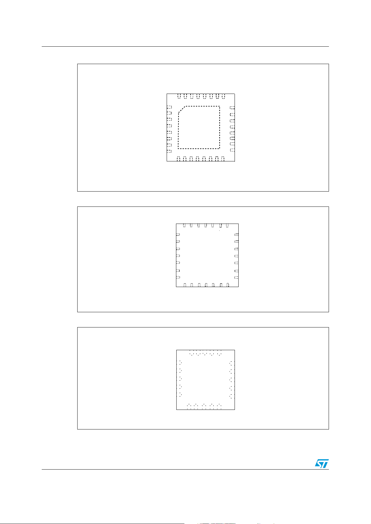
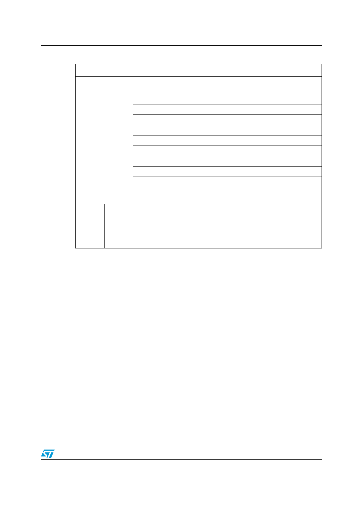
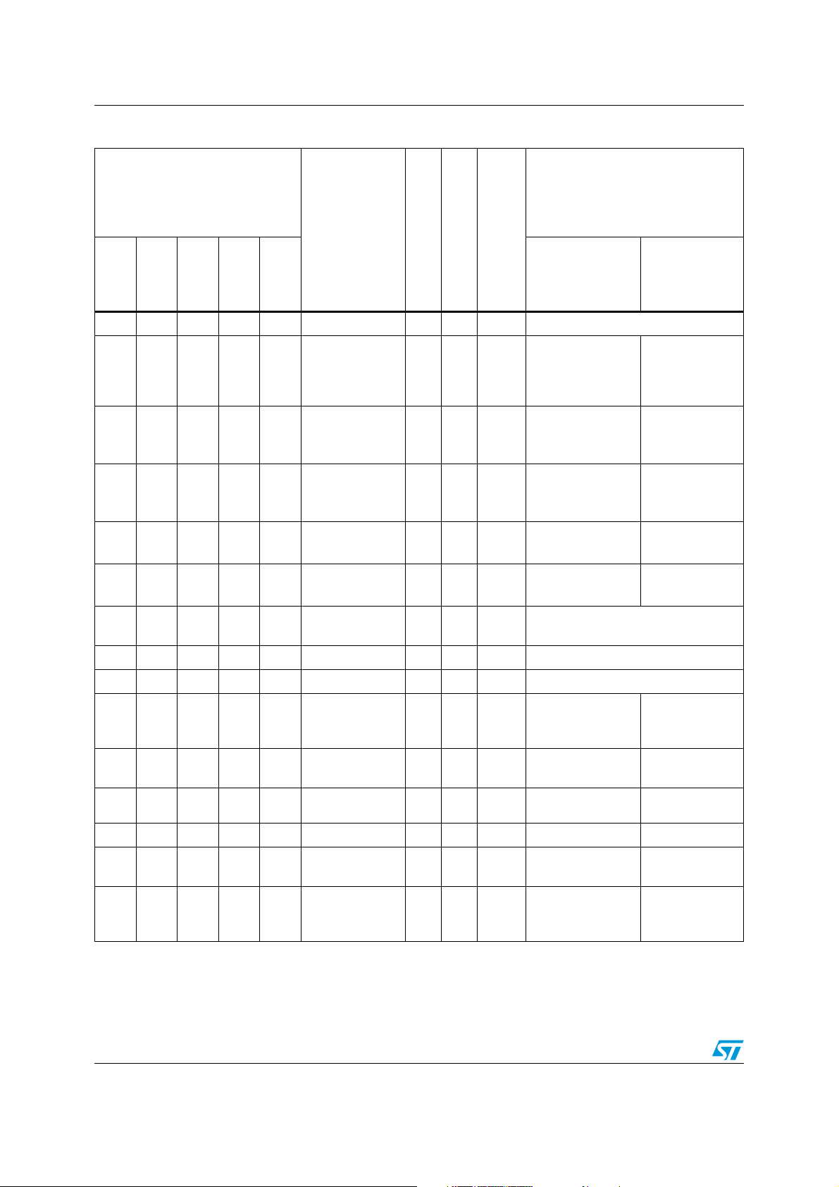
Figure 3. LQFP48 48-pin package pinout . . . . . . . . . . . . . . . . . . . . . . . . . . . . . . . . . . . . . . . . . . . . . 23
Figure 4. LQFP32 32-pin package pinout . . . . . . . . . . . . . . . . . . . . . . . . . . . . . . . . . . . . . . . . . . . . . 23
Figure 5. UFQFPN32 32-pin package pinout. . . . . . . . . . . . . . . . . . . . . . . . . . . . . . . . . . . . . . . . . . . 24
Figure 6. UFQFPN28 28-pin package pinout. . . . . . . . . . . . . . . . . . . . . . . . . . . . . . . . . . . . . . . . . . . 24
Figure 7. TSSOP20 20-pin package pinout . . . . . . . . . . . . . . . . . . . . . . . . . . . . . . . . . . . . . . . . . . . . 24
Figure 8. STM32F050xx memory map . . . . . . . . . . . . . . . . . . . . . . . . . . . . . . . . . . . . . . . . . . . . . . . 32
Figure 9. Pin loading conditions. . . . . . . . . . . . . . . . . . . . . . . . . . . . . . . . . . . . . . . . . . . . . . . . . . . . . 35
Figure 10. Pin input voltage . . . . . . . . . . . . . . . . . . . . . . . . . . . . . . . . . . . . . . . . . . . . . . . . . . . . . . . . . 35
Figure 11. Power supply scheme. . . . . . . . . . . . . . . . . . . . . . . . . . . . . . . . . . . . . . . . . . . . . . . . . . . . . 36
Figure 12. Current consumption measurement scheme . . . . . . . . . . . . . . . . . . . . . . . . . . . . . . . . . . . 36
Figure 13. High-speed external clock source AC timing diagram . . . . . . . . . . . . . . . . . . . . . . . . . . . . 52
Figure 14. Low-speed external clock source AC timing diagram . . . . . . . . . . . . . . . . . . . . . . . . . . . . . 53
Figure 15. Typical application with an 8 MHz crystal . . . . . . . . . . . . . . . . . . . . . . . . . . . . . . . . . . . . . . 55
Figure 16. Typical application with a 32.768 kHz crystal . . . . . . . . . . . . . . . . . . . . . . . . . . . . . . . . . . . 57
Figure 17. TC and TTa I/O input characteristics - CMOS port . . . . . . . . . . . . . . . . . . . . . . . . . . . . . . . 66
Figure 18. TC and TTa I/O input characteristics - TTL port . . . . . . . . . . . . . . . . . . . . . . . . . . . . . . . . . 66
Figure 19. Five volt tolerant (FT and FTf) I/O input characteristics - CMOS port. . . . . . . . . . . . . . . . . 67
Figure 20. Five volt tolerant (FT and FTf) I/O input characteristics - TTL port . . . . . . . . . . . . . . . . . . . 67
Figure 21. I/O AC characteristics definition . . . . . . . . . . . . . . . . . . . . . . . . . . . . . . . . . . . . . . . . . . . . . 70
Figure 22. Recommended NRST pin protection . . . . . . . . . . . . . . . . . . . . . . . . . . . . . . . . . . . . . . . . . 70
Figure 23. ADC accuracy characteristics . . . . . . . . . . . . . . . . . . . . . . . . . . . . . . . . . . . . . . . . . . . . . . . 73
Figure 24. Typical connection diagram using the ADC . . . . . . . . . . . . . . . . . . . . . . . . . . . . . . . . . . . . 73
Figure 25. I
Figure 26. SPI timing diagram - slave mode and CPHA = 0 . . . . . . . . . . . . . . . . . . . . . . . . . . . . . . . . 78
Figure 27. SPI timing diagram - slave mode and CPHA = 1
Figure 28. SPI timing diagram - master mode
Figure 29. I2S slave timing diagram (Philips protocol). . . . . . . . . . . . . . . . . . . . . . . . . . . . . . . . . . . . . 81
Figure 30. I2S master timing diagram (Philips protocol) . . . . . . . . . . . . . . . . . . . . . . . . . . . . . . . . . . . 81
Figure 31. LQFP48 - 7 x 7 mm, 48-pin low-profile quad flat package outline . . . . . . . . . . . . . . . . . . . 83
Figure 32. LQFP48 recommended footprint . . . . . . . . . . . . . . . . . . . . . . . . . . . . . . . . . . . . . . . . . . . . 84
Figure 33. LQFP32 - 7 x 7 mm, 32-pin low-profile quad flat package outline . . . . . . . . . . . . . . . . . . . 85
Figure 34. LQFP32 recommended footprint . . . . . . . . . . . . . . . . . . . . . . . . . . . . . . . . . . . . . . . . . . . . 86
Figure 35. UFQFPN32 - 5 x 5 mm, 32-lead ultra thin fine pitch quad flat no-lead package outline . . . 87
Figure 36. UFQFPN32 recommended footprint . . . . . . . . . . . . . . . . . . . . . . . . . . . . . . . . . . . . . . . . . . 88
Figure 37. UFQFPN28 - 4 x 4 mm, 28-lead ultra thin fine pitch quad flat no-lead package outline . . . 89
Figure 38. UFQFPN28 recommended footprint . . . . . . . . . . . . . . . . . . . . . . . . . . . . . . . . . . . . . . . . . . 90
Figure 39. TSSOP20 - 20-pin thin shrink small outline . . . . . . . . . . . . . . . . . . . . . . . . . . . . . . . . . . . . 91
Figure 40. TSSOP20 recommended footprint . . . . . . . . . . . . . . . . . . . . . . . . . . . . . . . . . . . . . . . . . . . 92
2
C bus AC waveforms and measurement circuit . . . . . . . . . . . . . . . . . . . . . . . . . . . . . . . . 77
(1)
(1)
. . . . . . . . . . . . . . . . . . . . . . . . . . . . . . . . . . . . . . . . . 79
. . . . . . . . . . . . . . . . . . . . . . . . . . . . . . 79
Doc ID 023079 Rev 3 7/98
Page 8
Introduction STM32F050xx
1 Introduction
This datasheet provides the ordering information and mechanical device characteristics of
the STM32F050x microcontrollers.
This STM32F050x4 and STM32F050x6 datasheet should be read in conjunction with the
STM32F0xxxx reference manual (RM0091). The reference manual is available from the
STMicroelectronics website www.st.com.
For information on the ARM Cortex™-M0 core, please refer to the Cortex™-M0 Technical
Reference Manual, available from the www.arm.com website at the following address:
http://infocenter.arm.com/help/index.jsp?topic=/com.arm.doc.ddi0432c/index.html.
8/98 Doc ID 023079 Rev 3
Page 9

STM32F050xx Description
2 Description
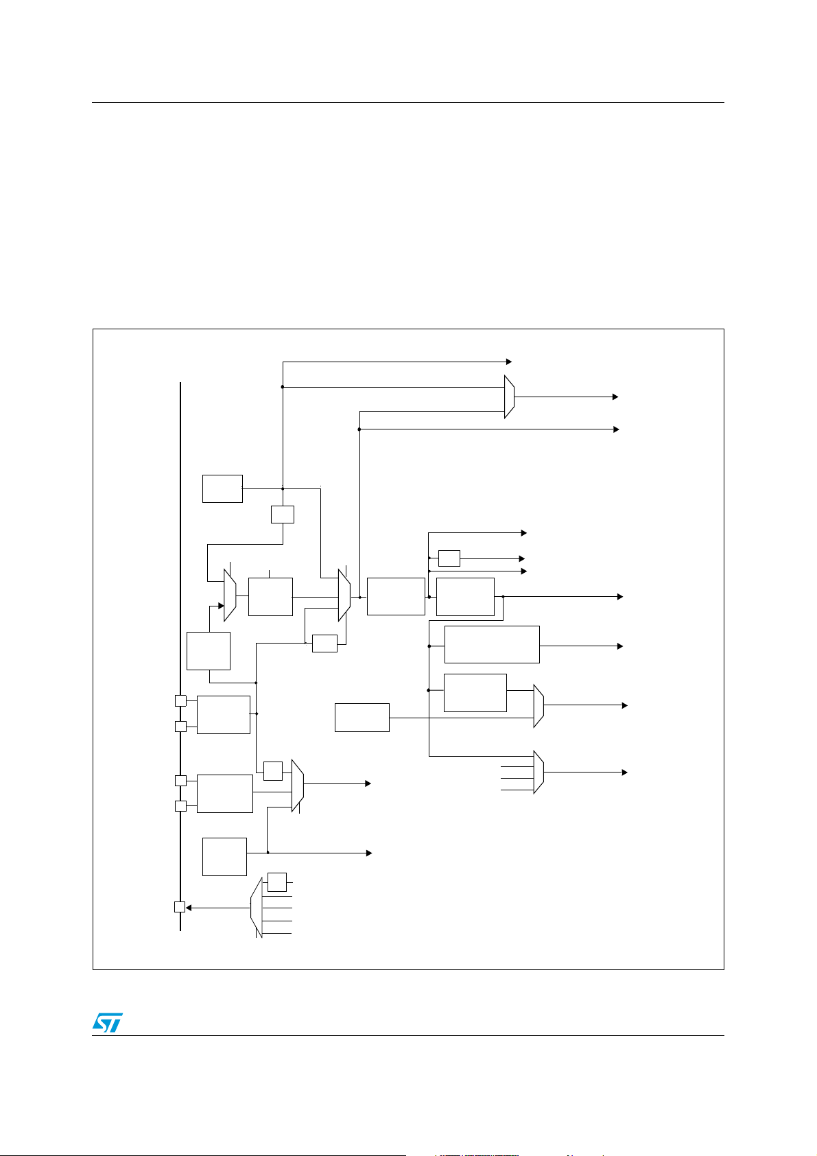
The STM32F050xx family incorporates the high-performance ARM Cortex™-M0 32-bit
RISC core operating at a 48 MHz maximum frequency, high-speed embedded memories
(Flash memory up to 32 Kbytes and SRAM up to 4 Kbytes), and an extensive range of
enhanced peripherals and I/Os. All devices offer standard communication interfaces (one
2
I
C, one SPI, one I2S, and one USART), one 12-bit ADC, up to five general-purpose 16-bit
timers, a 32-bit timer and an advanced-control PWM timer.
The STM32F050xx family operates in the -40 to +85 °C and -40 to +105 °C temperature
ranges, from a 2.0 to 3.6 V power supply. A comprehensive set of power-saving modes
allows the design of low-power applications.
The STM32F050xx family includes devices in five different packages ranging from 20 pins to
48 pins. Depending on the device chosen, different sets of peripherals are included. An
overview of the complete range of peripherals proposed in this family is provided.
These features make the STM32F050xx microcontroller family suitable for a wide range of
applications such as control application and user interfaces, handheld equipment, A/V
receivers and digital TV, PC peripherals, gaming and GPS platforms, industrial applications,
PLCs, inverters, printers, scanners, alarm systems, video intercoms, and HVACs.
Doc ID 023079 Rev 3 9/98
Page 10
Description STM32F050xx
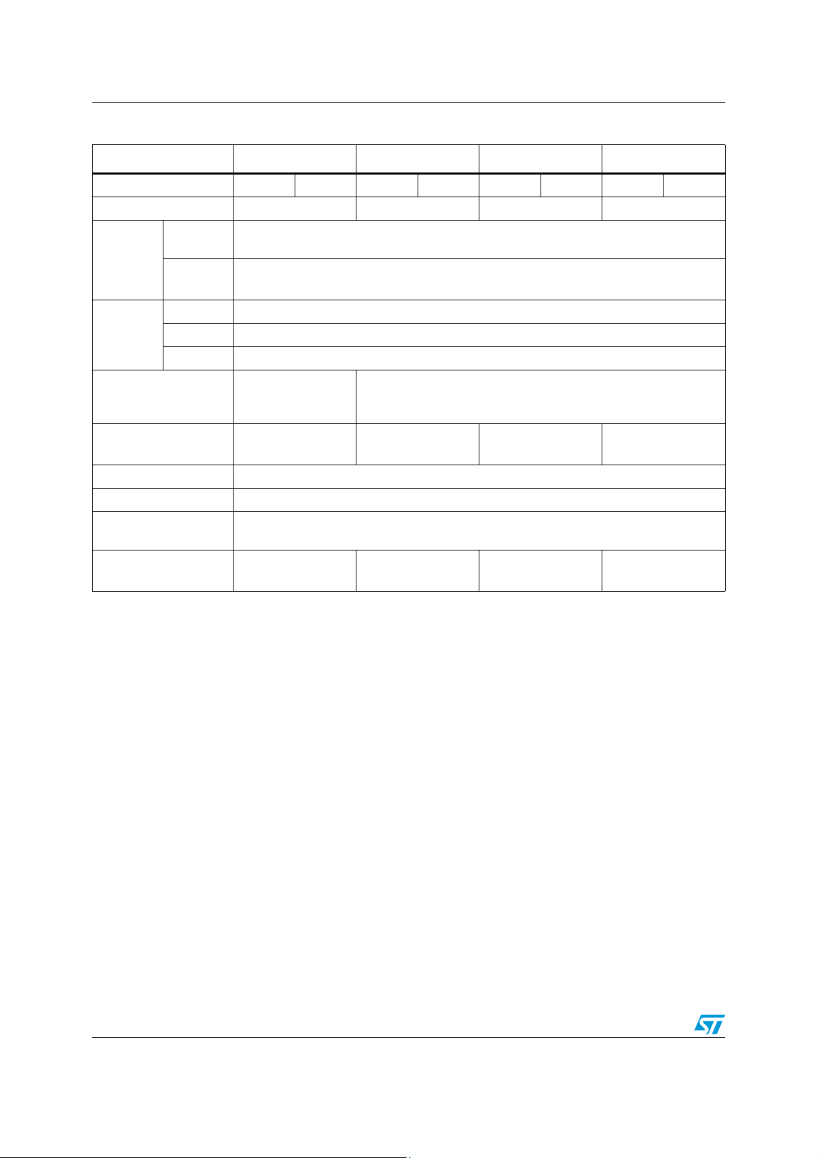
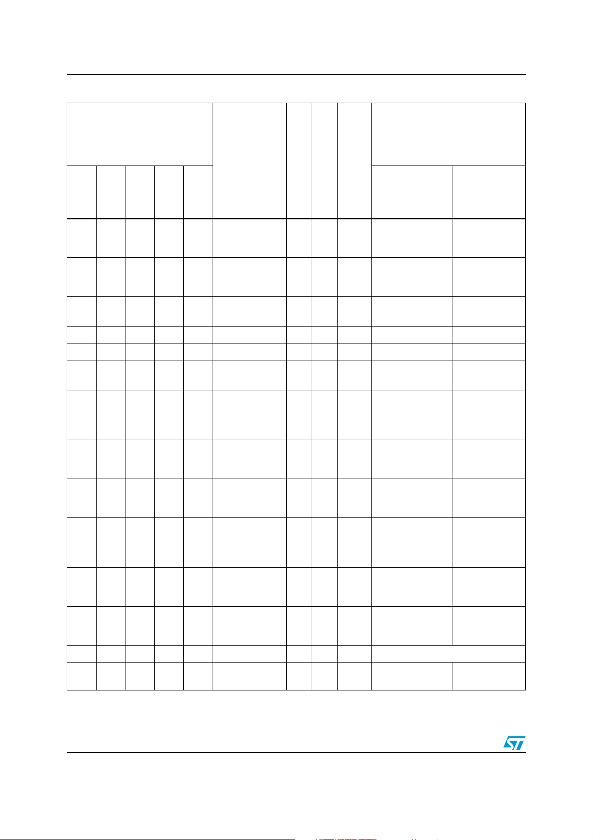
Table 2. STM32F050xx family device features and peripheral counts
Peripheral STM32F050Fx STM32F050Gx STM32F050Kx STM32F050Cx
Flash (Kbytes) 16 32 16 32 16 32 16 32
SRAM (Kbytes) 4 4 4 4
Timers
Comm.
interfaces
Advanced
control
General
purpose
SPI (I2S)
2
I
(1)
C1
1 (16-bit)
4 (16-bit)
1 (32-bit)
1
USART 1
12-bit synchronized
ADC
(number of channels)
GPIOs 13 21
1
(9 ext. + 3 int.)
1
(10 ext. + 3 int.)
25 (on LQFP32)
27 (on UFQFPN32)
39
Max. CPU frequency 48 MHz
Operating voltage 2.0 to 3.6 V
Operating temperature
Ambient operating temperature: -40 °C to 85 °C / -40 °C to 105 °C
Junction temperature: -40 °C to 125 °C
Packages TSSOP20 UFQFPN28
1. The SPI interface can be used either in SPI mode or in I2S audio mode.
LQFP32
UFQFPN32
LQFP48
10/98 Doc ID 023079 Rev 3
Page 11
STM32F050xx Description
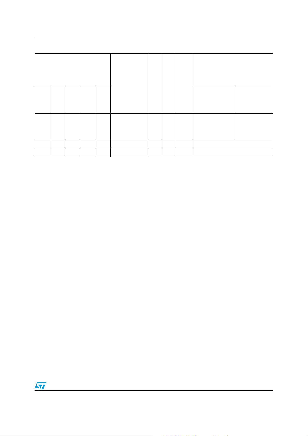
PA[ 15:0]
EXT.IT
NVIC
SWCLK
SWDAT
NRST
VDD=2 to 3.6V
39 AF
AHB
SRAM
WKUP
V
SS
GP DMA
5 channels
XTAL OSC
4-32 MHz
XTAL 32kHz
OSCIN - PF 0
OSCOUT - PF1
OSC32_OU T
OSC32_IN
AHBPCLK
HCLK
APBPCLK
FLASH
VOL T. RE G.
3.3 V T O1.8 V
V
DD18
POWER
RTC int erface
as AF
BusMatrix
32 bits
Int erfac e
4KB
RTC
CORTEX-M0 CPU
f
HCLK
= 48 MHz
obl
flash
Backup
reg
SCL,SDA,SMBal
I2C1
as AF
4channels
3 com pl . channels
BRK,ETR i nput as AF
4ch,ETRasAF
FCLK
Pow er
IWDG
@V
DD
@VSW
POR / PD R
SUPPLY
@V
DDA
V
DDA
V
BAT
=1.65 V to 3.6 V
RX,TX, CTS, RTS,
CK as A F
NVIC
SPI1/I2S1
Contr oll er
@V
DDA
SUPER VISION
PVD
Reset
Int
@V
DD
APB
POR
TAMPE R-RTC
RESET
& CLOCK
CONTROL
ADCCLK
PLL
(ALARM OUT)
Serial Wire
Debug
CECCLK
MISO/MCK,
PB[15:0]
PC[15:13]
PF[7:6, 1:0]
4ch,ETRasAF
1channelasAF
V
DD
32 KB
RC HS 14 MHz
USARTCLK
1 channel,
1compl,BRK asAF
1channel,
1compl,BRK as AF
controller
SRAM
SYSCFG IF
(20 mA f or FM+)
IR_OUT as AF
DBGMCU
AHB decoder
MS30246V2
TIMER 1
TIMER 2
TIMER 3
TIMER 14
TIMER 16
TIMER 17
USART1
GPIO port A
GPIO port B
GPIO port C
GPIO port F
12-bit ADC1
10
ADC_IN
V
DDA
Temp sensor
V
SSA
@V
DDA
IF
RC HS 8 MHz
RC LS
SCK/CK,
MOSI/SD,
NSS/WS as AF
WWDG
CRC
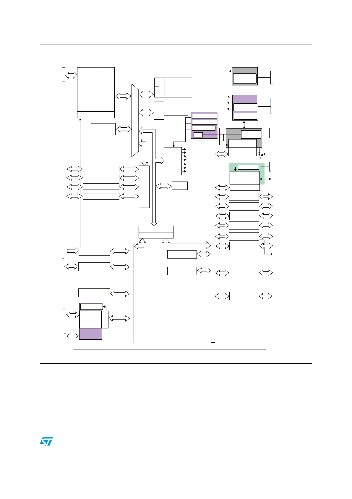
Figure 1. Block diagram
Doc ID 023079 Rev 3 11/98
Page 12

Functional overview STM32F050xx
3 Functional overview
3.1 ARM® CortexTM-M0 core with embedded Flash and SRAM
The ARM Cortex™-M0 processor is the latest generation of ARM processors for embedded
systems. It has been developed to provide a low-cost platform that meets the needs of MCU
implementation, with a reduced pin count and low-power consumption, while delivering
outstanding computational performance and an advanced system response to interrupts.
The ARM Cortex™-M0 32-bit RISC processor features exceptional code-efficiency,
delivering the high-performance expected from an ARM core in the memory size usually
associated with 8- and 16-bit devices.
The STM32F050xx family has an embedded ARM core and is therefore compatible with all
ARM tools and software.
Figure 1 shows the general block diagram of the device family.
3.2 Memories
The device has the following features:
● 4 Kbytes of embedded SRAM accessed (read/write) at CPU clock speed with 0 wait
states and featuring embedded parity checking with exception generation for fail-critical
applications.
● The non-volatile memory is divided into two arrays:
– 16 to 32 Kbytes of embedded Flash memory for programs and data
–Option bytes
The option bytes are used to write-protect the memory (with 4 KB granularity) and/or
readout-protect the whole memory with the following options:
– Level 0: no readout protection
– Level 1: memory readout protection, the Flash memory cannot be read from or
written to if either debug features are connected or boot in RAM is selected
– Level 2: chip readout protection, debug features (Cortex-M0 serial wire) and boot
in RAM selection disabled
3.3 Boot modes
At startup, the boot pin and boot selector option bit are used to select one of three boot
options:
● Boot from User Flash
● Boot from System Memory
● Boot from embedded SRAM
The boot loader is located in System Memory. It is used to reprogram the Flash memory by
using USART1.
12/98 Doc ID 023079 Rev 3
Page 13

STM32F050xx Functional overview
3.4 Cyclic redundancy check calculation unit (CRC)
The CRC (cyclic redundancy check) calculation unit is used to get a CRC code from a 32-bit
data word and a CRC-32 (Ethernet) polynomial.
Among other applications, CRC-based techniques are used to verify data transmission or
storage integrity. In the scope of the EN/IEC 60335-1 standard, they offer a means of
verifying the Flash memory integrity. The CRC calculation unit helps compute a signature of
the software during runtime, to be compared with a reference signature generated at link-
time and stored at a given memory location.
3.5 Power management
3.5.1 Power supply schemes
● V
= 2.0 to 3.6 V: external power supply for I/Os and the internal regulator.
DD
Provided externally through V
● V
= 2.0 to 3.6 V: external analog power supply for ADC, Reset blocks, RCs and PLL
DDA
(minimum voltage to be applied to V
voltage level must be always greater or equal to the V
provided first.
● V
= 1.6 to 3.6 V: power supply for RTC, external clock 32 kHz oscillator and backup
BAT
registers (through power switch) when V
3.5.2 Power supply supervisors
The device has integrated power-on reset (POR) and power-down reset (PDR) circuits.
They are always active, and ensure proper operation above a threshold of 2 V. The device
remains in reset mode when the monitored supply voltage is below a specified threshold,
V
POR/PDR
● The POR monitors only the V
● The PDR monitors both the V
The device features an embedded programmable voltage detector (PVD) that monitors the
V
DD
when V
threshold. The interrupt service routine can then generate a warning message and/or put
the MCU into a safe state. The PVD is enabled by software.
, without the need for an external reset circuit.
that V
should arrive first and be greater than or equal to VDD.
DDA
supply supervisor can be disabled (by programming a dedicated Option bit) to reduce
the power consumption if the application design ensures that V
equal to V
DD
.
power supply and compares it to the V
drops below the V
DD
PVD
pins.
DD
is 2.4 V when the ADC is used). The V
DDA
is not present.
DD
supply voltage. During the startup phase it is required
DD
DD
and V
supply voltages, however the V
DDA
threshold. An interrupt can be generated
PVD
threshold and/or when VDD is higher than the V
voltage level and must be
DD
DDA
is higher than or
DDA
PVD
DDA
power
Doc ID 023079 Rev 3 13/98
Page 14

Functional overview STM32F050xx
3.5.3 Voltage regulator
The regulator has three operating modes: main (MR), low power (LPR) and power down.
● MR is used in normal operating mode (Run)
● LPR can be used in Stop mode where the power demand is reduced
● Power down is used in Standby mode: the regulator output is in high impedance: the
kernel circuitry is powered down, inducing zero consumption (but the contents of the
registers and SRAM are lost)
This regulator is always enabled after reset. It is disabled in Standby mode, providing high
impedance output.
3.5.4 Low-power modes
The STM32F050xx family supports three low-power modes to achieve the best compromise
between low power consumption, short startup time and available wakeup sources:
● Sleep mode
In Sleep mode, only the CPU is stopped. All peripherals continue to operate and can
wake up the CPU when an interrupt/event occurs.
● Stop mode
Stop mode achieves very low power consumption while retaining the content of SRAM
and registers. All clocks in the 1.8 V domain are stopped, the PLL, the HSI RC and the
HSE crystal oscillators are disabled. The voltage regulator can also be put either in
normal or in low power mode.
The device can be woken up from Stop mode by any of the EXTI lines. The EXTI line
source can be one of the 16 external lines, the PVD output, RTC alarm, I2C1 or
USART1.
The I2C1 and the USART1 can be configured to enable the HSI RC oscillator for
processing incoming data. If this is used, the voltage regulator should not be put in the
low-power mode but kept in normal mode.
● Standby mode
The Standby mode is used to achieve the lowest power consumption. The internal
voltage regulator is switched off so that the entire 1.8 V domain is powered off. The
PLL, the HSI RC and the HSE crystal oscillators are also switched off. After entering
Standby mode, SRAM and register contents are lost except for registers in the Backup
domain and Standby circuitry.
The device exits Standby mode when an external reset (NRST pin), a IWDG reset, a
rising edge on the WKUP pins, or an RTC alarm occurs.
Note: The RTC, the IWDG, and the corresponding clock sources are not stopped by entering Stop
or Standby mode.
14/98 Doc ID 023079 Rev 3
Page 15
STM32F050xx Functional overview
3.6 Clocks and startup
System clock selection is performed on startup, however the internal RC 8 MHz oscillator is
selected as default CPU clock on reset. An external 4-32 MHz clock can be selected, in
which case it is monitored for failure. If failure is detected, the system automatically switches
back to the internal RC oscillator. A software interrupt is generated if enabled. Similarly, full
interrupt management of the PLL clock entry is available when necessary (for example on
failure of an indirectly used external crystal, resonator or oscillator).
Several prescalers allow the application to configure the frequency of the AHB and the APB
domains. The maximum frequency of the AHB and the APB domains is 48 MHz.
Figure 2. Clock tree
FLITFCLK
to Flash programming interface
HSI
SYSCLK
to I2C1
to I2S1
OSC_OUT
OSC_IN
OSC32_IN
OSC32_OUT
MCO
8 MHz
HSI RC
PLLSRC
/1,2,
3,..16
4-32 MHz
HSE OSC
LSE OSC
32.768kHz
LSI RC
40kHz
Main clock
output
HSI
PLLMUL
PLL
x2,x3,..
x16
/32
LSE
MCO
/2
HSI
PLLCLK
HSE
CSS
RTCCLK
RTCSEL[1:0]
LSI
/2
PLLCLK
HSI
HSI14
HSE
SYSCLK
SW
prescaler
/1,2,..512
SYSCLK
14 MHz
HSI14 RC
AHB
AHB
HSI14
to RTC
to IWWDG
IWWDGCLK
HCLK
/8
APB
prescaler
/1,2,4,8,16
If (APB1 prescaler
=1) x1 else x2
ADC
Prescaler
/2,4
PCLK
SYSCLK
HSI
LSE
to AHB bus, core,
memory and DMA
to cortex System timer
FHCLK Cortex free running clock
PCLK
to APB peripherals
to TIM1,2,3,
14,16,17
to ADC
14 MHz max
to USART1
MS30247V1
Doc ID 023079 Rev 3 15/98
Page 16

Functional overview STM32F050xx
3.7 General-purpose inputs/outputs (GPIOs)
Each of the GPIO pins can be configured by software as output (push-pull or open-drain), as
input (with or without pull-up or pull-down) or as peripheral alternate function. Most of the
GPIO pins are shared with digital or analog alternate functions.
The I/O configuration can be locked if needed following a specific sequence in order to avoid
spurious writing to the I/Os registers.
3.8 Direct memory access controller (DMA)
The 5-channel general-purpose DMAs manage memory-to-memory, peripheral-to-memory
and memory-to-peripheral transfers.
The DMA supports circular buffer management, removing the need for user code
intervention when the controller reaches the end of the buffer.
Each channel is connected to dedicated hardware DMA requests, with support for software
trigger on each channel. Configuration is made by software and transfer sizes between
source and destination are independent.
DMA can be used with the main peripherals: SPI, I2S, I2C, USART, all TIMx timers (except
TIM14) and ADC.
3.9 Interrupts and events
3.9.1 Nested vectored interrupt controller (NVIC)
The STM32F050xx family embeds a nested vectored interrupt controller able to handle up
to 32 maskable interrupt channels (not including the 16 interrupt lines of Cortex™-M0) and 4
priority levels.
● Closely coupled NVIC gives low latency interrupt processing
● Interrupt entry vector table address passed directly to the core
● Closely coupled NVIC core interface
● Allows early processing of interrupts
● Processing of late arriving higher priority interrupts
● Support for tail-chaining
● Processor state automatically saved
● Interrupt entry restored on interrupt exit with no instruction overhead
This hardware block provides flexible interrupt management features with minimal interrupt
latency.
3.9.2 Extended interrupt/event controller (EXTI)
The external interrupt/event controller consists of 24 edge detector lines used to generate
interrupt/event requests and wake-up the system. Each line can be independently
configured to select the trigger event (rising edge, falling edge, both) and can be masked
independently. A pending register maintains the status of the interrupt requests. The EXTI
can detect an external line with a pulse width shorter than the internal clock period. Up to 39
GPIOs can be connected to the 16 external interrupt lines.
16/98 Doc ID 023079 Rev 3
Page 17
STM32F050xx Functional overview
3.10 Analog to digital converter (ADC)
The 12-bit analog to digital converter has up to 16 external and 3 internal (temperature
sensor, voltage reference, VBAT voltage measurement) channels and performs conversions
in single-shot or scan modes. In scan mode, automatic conversion is performed on a
selected group of analog inputs.
The ADC can be served by the DMA controller.
An analog watchdog feature allows very precise monitoring of the converted voltage of one,
some or all selected channels. An interrupt is generated when the converted voltage is
outside the programmed thresholds.
3.10.1 Temperature sensor
The temperature sensor (TS) generates a voltage V
that varies linearly with
SENSE
temperature.
The temperature sensor is internally connected to the ADC_IN16 input channel which is
used to convert the sensor output voltage into a digital value.
The sensor provides good linearity but it has to be calibrated to obtain good overall accuracy
of the temperature measurement. As the offset of the temperature sensor varies from chip
to chip due to process variation, the uncalibrated internal temperature sensor is suitable for
applications that detect temperature changes only.
To improve the accuracy of the temperature sensor measurement, each device is
individually factory-calibrated by ST. The temperature sensor factory calibration data are
stored by ST in the system memory area, accessible in read-only mode.
Table 3. Temperature sensor calibration values
Calibration value name Description Memory address
TS ADC raw data acquired at
TS_CAL1
TS_CAL2
temperature of 30 °C,
V
= 3.3 V
DDA
TS ADC raw data acquired at
temperature of 110 °C
V
= 3.3 V
DDA
0x1FFF F7B8 - 0x1FFF F7B9
0x1FFF F7C2 - 0x1FFF F7C3
3.10.2 Internal voltage reference (V
The internal voltage reference (V
ADC. V
of V
REFINT
is internally connected to the ADC_IN17 input channel. The precise voltage
REFINT
is individually measured for each part by ST during production test and stored in
the system memory area. It is accessible in read-only mode.
Table 4. Temperature sensor calibration values
Calibration value name Description Memory address
VREFINT_CAL
REFINT
Raw data acquired at
temperature of 30 °C
V
DDA
Doc ID 023079 Rev 3 17/98
REFINT
)
) provides a stable (bandgap) voltage output for the
0x1FFF F7BA - 0x1FFF F7BB
= 3.3 V
Page 18
Functional overview STM32F050xx
3.11 Timers and watchdogs
The STM32F050xx family devices include up to six general-purpose timers, one basic timer
and an advanced control timer.
Ta bl e 5 compares the features of the advanced-control, general-purpose and basic timers.
Table 5. Timer feature comparison
Timer
type
Advanced
control
General
purpose
Timer
TIM1 16-bit
TIM2 32-bit
TIM3 16-bit
TIM14 16-bit Up
TIM16,
TIM17
Counter
resolution
16-bit Up
Counter
type
Up, down,
up/down
Up, down,
up/down
Up, down,
up/down
Prescaler
factor
Any integer
between 1
and 65536
Any integer
between 1
and 65536
Any integer
between 1
and 65536
Any integer
between 1
and 65536
Any integer
between 1
and 65536
3.11.1 Advanced-control timer (TIM1)
The advanced-control timer (TIM1) can be seen as a three-phase PWM multiplexed on 6
channels. It has complementary PWM outputs with programmable inserted dead times. It
can also be seen as a complete general-purpose timer. The 4 independent channels can be
used for:
● Input capture
● Output compare
● PWM generation (edge or center-aligned modes)
● One-pulse mode output
DMA request
generation
Ye s 4 Ye s
Ye s 4 N o
Ye s 4 N o
No 1 No
Ye s 1 Ye s
Capture/compare
channels
Complementary
outputs
If configured as a standard 16-bit timer, it has the same features as the TIMx timer. If
configured as the 16-bit PWM generator, it has full modulation capability (0-100%).
The counter can be frozen in debug mode.
Many features are shared with those of the standard timers which have the same
architecture. The advanced control timer can therefore work together with the other timers
via the Timer Link feature for synchronization or event chaining.
3.11.2 General-purpose timers (TIM2..3, TIM14..17)
There are six synchronizable general-purpose timers embedded in the STM32F050xx
devices (see Ta bl e 5 for differences). Each general-purpose timer can be used to generate
PWM outputs, or as simple time base.
18/98 Doc ID 023079 Rev 3
Page 19

STM32F050xx Functional overview
TIM2, TIM3
STM32F050xx devices feature two synchronizable 4-channel general-purpose timers. TIM2
is based on a 32-bit auto-reload up/downcounter and a 16-bit prescaler. TIM3 is based on a
16-bit auto-reload up/downcounter and a 16-bit prescaler. They feature 4 independent
channels each for input capture/output compare, PWM or one-pulse mode output. This
gives up to 12 input captures/output compares/PWMs on the largest packages.
The TIM2 and TIM3 general-purpose timers can work together or with the TIM1 advanced-
control timer via the Timer Link feature for synchronization or event chaining.
TIM2 and TIM3 both have independent DMA request generation.
These timers are capable of handling quadrature (incremental) encoder signals and the
digital outputs from 1 to 3 hall-effect sensors.
Their counters can be frozen in debug mode.
TIM14
This timer is based on a 16-bit auto-reload upcounter and a 16-bit prescaler.
TIM14 features one single channel for input capture/output compare, PWM or one-pulse
mode output.
Its counter can be frozen in debug mode.
TIM16 and TIM17
These timers are based on a 16-bit auto-reload upcounter and a 16-bit prescaler.
TIM16 and TIM17 feature one single channel for input capture/output compare, PWM or
one-pulse mode output.
The TIM16 and TIM17 timers can work together via the Timer Link feature for
synchronization or event chaining.
TIM16, and TIM17 have a complementary output with dead-time generation and
independent DMA request generation
Their counters can be frozen in debug mode.
3.11.3 Independent watchdog (IWDG)
The independent watchdog is based on an 8-bit prescaler and 12-bit downcounter with user-
defined refresh window. It is clocked from an independent 40 kHz internal RC and as it
operates independently from the main clock, it can operate in Stop and Standby modes. It
can be used either as a watchdog to reset the device when a problem occurs, or as a free
running timer for application timeout management. It is hardware or software configurable
through the option bytes. The counter can be frozen in debug mode.
3.11.4 System window watchdog (WWDG)
The system window watchdog is based on a 7-bit downcounter that can be set as free
running. It can be used as a watchdog to reset the device when a problem occurs. It is
clocked from the APB clock (PCLK). It has an early warning interrupt capability and the
counter can be frozen in debug mode.
Doc ID 023079 Rev 3 19/98
Page 20

Functional overview STM32F050xx
3.11.5 SysTick timer
This timer is dedicated to real-time operating systems, but could also be used as a standard
down counter. It features:
● A 24-bit down counter
● Autoreload capability
● Maskable system interrupt generation when the counter reaches 0.
● Programmable clock source (HCLK or HCLK/8)
3.12 Real-time clock (RTC) and backup registers
The RTC and the 5 backup registers are supplied through a switch that takes power either
on V
registers used to store 20 bytes of user application data when V
They are not reset by a system or power reset, or when the device wakes up from Standby
mode.
The RTC is an independent BCD timer/counter. Its main features are the following:
● Calendar with subsecond, seconds, minutes, hours (12 or 24 format), week day, date,
● Automatically correction for 28, 29 (leap year), 30, and 31 day of the month.
● Programmable alarm with wake up from Stop and Standby mode capability.
● On-the-fly correction from 1 to 32767 RTC clock pulses. This can be used to
● Digital calibration circuit with 1 ppm resolution, to compensate for quartz crystal
● 2 anti-tamper detection pins with programmable filter. The MCU can be woken up from
● Timestamp feature which can be used to save the calendar content. This function can
supply when present or through the V
DD
pin. The backup registers are five 32-bit
BAT
power is not present.
DD
month, year, in BCD (binary-coded decimal) format.
synchronize it with a master clock.
inaccuracy.
Stop and Standby modes on tamper event detection.
triggered by an event on the timestamp pin, or by a tamper event. The MCU can be
woken up from Stop and Standby modes on timestamp event detection.
The RTC clock sources can be:
● A 32.768 kHz external crystal
● A resonator or oscillator
● The internal low-power RC oscillator (typical frequency of 40 kHz)
● The high-speed external clock divided by 32.
3.13 Inter-integrated circuit interface (I2C)
The I2C interface (I2C1) can operate in multimaster or slave mode. It can support Standard
mode (up to 100 kbit/s), Fast mode (up to 400 kbit/s) and Fast Mode Plus (up to 1 Mbit/s)
with 20 mA output drive.
It supports 7-bit and 10-bit addressing modes, multiple 7-bit slave addresses (2 addresses,
1 with configurable mask). It also includes programmable analog and digital noise filters.
20/98 Doc ID 023079 Rev 3
Page 21

STM32F050xx Functional overview
Table 6. Comparison of I2C analog and digital filters
Analog filter Digital filter
Pulse width of
suppressed spikes
Benefits Available in Stop mode
Drawbacks
50 ns
Variations depending on
temperature, voltage, process
Programmable length from 1 to 15
I2C peripheral clocks
1. Extra filtering capability vs.
standard requirements.
2. Stable length
Wakeup from Stop on address
match is not available when digital
filter is enabled.
In addition, I2C1 provides hardware support for SMBUS 2.0 and PMBUS 1.1: ARP
capability, Host notify protocol, hardware CRC (PEC) generation/verification, timeouts
verifications and ALERT protocol management. I2C1 also has a clock domain independent
from the CPU clock, allowing the I2C1 to wake up the MCU from Stop mode on address
match.
The I2C interface can be served by the DMA controller.
3.14 Universal synchronous/asynchronous receiver transmitter
(USART)
The device embeds an universal synchronous/asynchronous receiver transmitters
(USART1), which communicates at speeds of up to 6 Mbit/s.
It provides hardware management of the CTS, RTS and RS485 DE signals, multiprocessor
communication mode, master synchronous communication and single-wire half-duplex
communication mode. It also supports SmartCard communication (ISO 7816), IrDA SIR
ENDEC, LIN Master/Slave capability, auto baud rate feature and has a clock domain
independent from the CPU clock, allowing it to wake up the MCU from Stop mode.
The USART interface can be served by the DMA controller.
3.15 Serial peripheral interface (SPI)/Inter-integrated sound
interfaces (I
The SPI (SPI1) is able to communicate up to 18 Mbits/s in slave and master modes in full-
duplex and half-duplex communication modes. The 3-bit prescaler gives 8 master mode
frequencies and the frame size is configurable from 4 bits to 16 bits.
One standard I
can operate as master or slave at half-duplex communication mode. It can be configured to
transfer 16 and 24 or 32 bits with16-bit or 32-bit data resolution and synchronized by a
specific signal. Audio sampling frequency from 8 kHz up to 192 kHz can be set by 8-bit
programmable linear prescaler. When operating in master mode it can output a clock for an
external audio component at 256 times the sampling frequency.
2
S)
2
S interface (multiplexed with SPI1) supporting four different audio standards
Doc ID 023079 Rev 3 21/98
Page 22

Functional overview STM32F050xx
3.16 Serial wire debug port (SW-DP)
An ARM SW-DP interface is provided to allow a serial wire debugging tool to be connected
to the MCU.
22/98 Doc ID 023079 Rev 3
Page 23
STM32F050xx Pinouts and pin description
44 43 42 41 40 39 38 37
36
35
34
33
32
31
30
29
28
27
26
25
24
23
12
13 14 15 16 17 18
19 20 21 22
1
2
3
4
5
6
7
8
9
10
11
48 47 46 45
LQFP48
PA3
PA4
PA5
PA6
PA7
PB0
PB1
PB2
PB10
PB11
VSS
VDD
PF7
PF6
PA13
PA12
PA11
PA10
PA9
PA8
PB15
PB14
PB13
PB12
VBAT
NRST
VSSA
VDDA
PA0
PA1
PA2
VDD
VSS
PB9
PB8
BOOT0
PB7
PB6
PB5
PB4
PB3
PA15
PA14
MS19842V1
PC13
PC14/OSC32_IN
PF0/OSC_IN
PF1/OSC_OUT
PC15/OSC32_OUT
MS30475V1
32 31 30 29 28 27 26 25
24
23
22
20
19
18
17
8
910111213
14 15 16
1
2
3
4
5
6
7
LQFP32
PA3
PA4
PA5
PA6
PA7
PB0
PB1
VSS
PA14
PA13
PA12
PA11
PA10
PA9
PA8
VDD
NRST
VDDA
PA0
PA1
PA2
VSS
BOOT0
PB7
PB6
PB5
PB4
PB3
PA15
PF0/OSC_IN
PF1/OSC_OUT
VDD
21
4 Pinouts and pin description
Figure 3. LQFP48 48-pin package pinout
Figure 4. LQFP32 32-pin package pinout
1. PB2 and PB8 should be treated as unconnected pins on the LQFP32 package (even when they are not
available on the package, they are not forced to a defined level by hardware).
Doc ID 023079 Rev 3 23/98
Page 24
Pinouts and pin description STM32F050xx
PA5
PA6
PA7
PA7
PA2
PA3
PA4
VDDA
BOOT0
PF0/OSC_IN
NRST
VDD
VDD
VSS
PB1
PA8
PA10
PA9
PB4
PB3
PA15
PA8
PB 7
PB6
PB5
2
1
3
4
5
6
7
981011121314
20
21
19
18
17
16
15
2728 26 25 24 23 22
PF1/OSC_OUT
MS30967V1
PA0
PA1
2
1
3
4
5
67 8
9
PA0
PF0/OSC_IN
PA1
BOOT0
PA10
PA9
VDD
PB5
PA6
PA7
PB1
VSS
PA2
PA3
10
PA 4
PA13
MS30968V1
PF1/OSC_OUT
NRST
VDDA
PA13
20 19 18 17 16
15
14
13
12
11
Figure 5. UFQFPN32 32-pin package pinout
PB4
PB0
PB3
PB1
PA15
24
23
22
21
20
19
18
17
PB2
PA14
PA13
PA12
PA11
PA10
PA9
PA8
VDD
MS19844V2
VDD
PF0/OSC_IN
PF1/OSC_OUT
NRST
VDDA
PA0
PA1
PA2
PB7
VSS
VSSA
1291011
PA6
PA5
PB5
PB6
28
13 1 4 15 16
PA7
BOOT0
PB8
31 30 29
32 27 26 25
1
0
2
3
4
5
6
7
8
PA3
PA4
Figure 6. UFQFPN28 28-pin package pinout
Figure 7. TSSOP20 20-pin package pinout
24/98 Doc ID 023079 Rev 3
Page 25
STM32F050xx Pinouts and pin description
Table 7. Legend/abbreviations used in the pinout table
Name Abbreviation Definition
Pin name
Pin type
I/O structure
Pin
functions
Notes
Alternate
functions
Additional
functions
Unless otherwise specified in brackets below the pin name, the pin function
during and after reset is the same as the actual pin name
S Supply pin
I Input only pin
I/O Input / output pin
FT 5 V tolerant I/O
FTf 5 V tolerant I/O, FM+ capable
TTa 3.3 V tolerant I/O directly connected to ADC
TC Standard 3.3V I/O
B Dedicated BOOT0 pin
RST Bidirectional reset pin with embedded weak pull-up resistor
Unless otherwise specified by a note, all I/Os are set as floating inputs during
and after reset
Functions selected through GPIOx_AFR registers
Functions directly selected/enabled through peripheral registers
Doc ID 023079 Rev 3 25/98
Page 26
Pinouts and pin description STM32F050xx
Table 8. Pin definitions
Pin number
Pin functions
Pin name
(function after
reset)
Pin type
I/O structure
Notes
Alternate
functions
LQFP48
LQFP32
UFQFPN32
UFQFPN28
TSSOP20
1 - - - - VBAT S Backup power supply
2-- - - PC13 I/OTC
(1)(2)
PC14-
3-- - -
OSC32_IN
I/O TC
(1)(2)
(PC14)
PC15-
4-- - -
OSC32_OUT
I/O TC
(1)(2)
(PC15)
52222
PF0-OSC_IN
(PF0)
I/O FT OSC_IN
Additional
functions
RTC_TAMP1,
RTC_TS,
RTC_OUT,
WKUP2
OSC32_IN
OSC32_OUT
63333
74444 NRST I/ORST
PF1-OSC_OUT
(PF1)
I/O FT OSC_OUT
Device reset input / internal reset
output (active low)
8 - 0 - - VSSA S Analog ground
9 5 5 5 5 VDDA S Analog power supply
ADC_IN0,
10 6 6 6 6 PA0 I/O TTa TIM2_CH1_ETR
RTC_TAMP2,
WKUP1
117777 PA1 I/OTTa
TIM2_CH2,
EVENTOUT
ADC_IN1
12 8 8 8 8 PA2 I/O TTa TIM2_CH3 ADC_IN2
13 9 9 9 9 PA3 I/O TTa TIM2_CH4 ADC_IN3
14 10 10 10 10 PA4 I/O TTa
SPI1_NSS/I2S1_
WS, TIM14_CH1
ADC_IN4
SPI1_SCK/I2S1_
15 11 11 11 11 PA5 I/O TTa
CK,
ADC_IN5
TIM2_CH1_ETR
26/98 Doc ID 023079 Rev 3
Page 27
STM32F050xx Pinouts and pin description
Table 8. Pin definitions (continued)
Pin number
Pin functions
Pin name
(function after
reset)
LQFP48
LQFP32
UFQFPN32
16 12 12 12 12 PA6 I/O TTa
17 13 13 13 13 PA7 I/O TTa
TSSOP20
UFQFPN28
Pin type
I/O structure
Notes
Alternate
functions
SPI1_MISO/I2S1_
MCK, TIM3_CH1,
TIM1_BKIN,
TIM16_CH1,
EVENTOUT
SPI1_MOSI/I2S1_
SD, TIM3_CH2,
TIM14_CH1,
TIM1_CH1N,
TIM17_CH1,
EVENTOUT
Additional
functions
ADC_IN6
ADC_IN7
TIM3_CH3,
18 14 14 14 14 PB0 I/O TTa
19 15 15 15 15 PB1 I/O TTa
20 - 16 - - PB2 I/O FT
21---- PB10 I/OFT TIM2_CH3
22---- PB11 I/OFT
23 16 0 16 15 VSS S Ground
24 17 17 17 16 VDD S Digital power supply
25---- PB12 I/OFT
26 - - - - PB13 I/O FT TIM1_CH1N,
27---- PB14 I/OFT TIM1_CH2N
28 - - - - PB15 I/O FT TIM1_CH3N, RTC_REFIN
29 18 18 18 - PA8 I/O FT
30 19 19 19 17 PA9 I/O FT
31 20 20 20 18 PA10 I/O FT
(3)
TIM1_CH2N,
EVENTOUT
TIM3_CH4,
TIM14_CH1,
TIM1_CH3N
TIM2_CH4,
EVENTOUT
TIM1_BKIN,
EVENTOUT
USART1_CK,
TIM1_CH1,
EVENTOUT, MCO
USART1_TX,
TIM1_CH2
USART1_RX,
TIM1_CH3,
TIM17_BKIN
ADC_IN8
ADC_IN9
Doc ID 023079 Rev 3 27/98
Page 28
Pinouts and pin description STM32F050xx
Table 8. Pin definitions (continued)
Pin number
Pin functions
Pin name
(function after
LQFP48
LQFP32
UFQFPN32
UFQFPN28
reset)
TSSOP20
Pin type
32 21 21 - - PA11 I/O FT
33 22 22 - - PA12 I/O FT
I/O structure
Notes
Alternate
functions
USART1_CTS,
TIM1_CH4,
EVENTOUT
USART1_RTS,
TIM1_ETR,
EVENTOUT
Additional
functions
34 23 23 21 19
PA 13
(SWDAT)
I/O FT
(4)
IR_OUT, SWDAT
35---- PF6 I/OFT
36---- PF7 I/OFT
37 24 24 22 20
PA 14
(SWCLK)
I/O FT
(4)
SWCLK
SPI1_NSS/I2S1_
38 25 25 23 - PA15 I/O FT
WS,
TIM2_CH_ETR,
EVENTOUT
SPI1_SCK/I2S1_
39 26 26 - - PB3 I/O FT
CK, TIM2_CH2,
EVENTOUT
SPI1_MISO/I2S1_
40 27 27 - - PB4 I/O FT
MCK, TIM3_CH1,
EVENTOUT
SPI1_MOSI/I2S1_
41 28 28 24 - PB5 I/O FT
SD, I2C1_SMBA,
TIM16_BKIN,
TIM3_CH2
I2C1_SCL,
42 29 29 25 - PB6 I/O FTf
USART1_TX,
TIM16_CH1N
I2C1_SDA,
43 30 30 26 - PB7 I/O FTf
USART1_RX,
TIM17_CH1N
44 31 31 27 1 BOOT0 I B Boot memory selection
45 - 32 - - PB8 I/O FTf
28/98 Doc ID 023079 Rev 3
(3)
I2C1_SCL,
TIM16_CH1
Page 29
STM32F050xx Pinouts and pin description
Table 8. Pin definitions (continued)
Pin number
Pin functions
Pin name
(function after
LQFP48
LQFP32
UFQFPN32
UFQFPN28
reset)
TSSOP20
Pin type
46---- PB9 I/OFTf
47 32 0 28 - VSS S Ground
48 1 1 1 - VDD S Digital power supply
1. PC13, PC14 and PC15 are supplied through the power switch. Since the switch only sinks a limited amount of current
(3 mA), the use of GPIO PC13 to PC15 in output mode is limited:
- The speed should not exceed 2 MHz with a maximum load of 30 pF
- these GPIOs must not be used as a current sources (e.g. to drive an LED).
2. After the first backup domain power-up, PC13, PC14 and PC15 operate as GPIOs. Their function then depends on the
content of the Backup registers which is not reset by the main reset. For details on how to manage these GPIOs, refer to
the Battery backup domain and BKP register description sections in the STM32F05xx reference manual.
3. PB2 and PB8 should be treated as unconnected pins on the LQFP32 package (even when they are not available on the
package, they are not forced to a defined level by hardware).
4. After reset, these pins are configured as SWDAT and SWCLK alternate functions, and the internal pull-up on SWDAT pin
and internal pull-down on SWCLK pin are activated.
I/O structure
Notes
Alternate
functions
I2C1_SDA,
IR_OUT,
TIM17_CH1,
EVENTOUT
Additional
functions
Doc ID 023079 Rev 3 29/98
Page 30
30/98 Doc ID 023079 Rev 3
Table 9. Alternate functions selected through GPIOA_AFR registers for port A
Pin name AF0 AF1 AF2 AF3 AF4 AF5 AF6 AF7
Pinouts and pin description STM32F050xx
PA 0
TIM2_CH1_
ETR
PA1 EVENTOUT TIM2_CH2
PA2 TIM2_CH3
PA3 TIM2_CH4
PA 4
PA 5
PA 6
PA 7
SPI1_NSS/
I2S1_WS
SPI1_SCK/
I2S1_CK
SPI1_MISO/
I2S1_MCK
SPI1_MOSI/
I2S1_SD
CEC
TIM2_CH1_
ETR
TIM3_CH1 TIM1_BKIN TIM16_CH1 EVENTOUT
TIM3_CH2 TIM1_CH1N TIM14_CH1 TIM17_CH1 EVENTOUT
PA8 MCO USART1_CK TIM1_CH1 EVENTOUT
PA9 USART1_TX TIM1_CH2
PA10 TIM17_BKIN USART1_RX TIM1_CH3
PA11 EVENTOUT USART1_CTS TIM1_CH4
PA12 EVENTOUT USART1_RTS TIM1_ETR
PA 13 S W DAT I R_ O U T
TIM14_CH1
PA 14 S W CL K
PA 15
SPI1_NSS/
I2S1_WS
TIM2_CH1_
ETR
EVENTOUT
Page 31

Table 10. Alternate functions selected through GPIOB_AFR registers for port B
Pin name AF0 AF1 AF2 AF3
PB0 EVENTOUT TIM3_CH3 TIM1_CH2N
PB1 TIM14_CH1 TIM3_CH4 TIM1_CH3N
PB2
PB3 SPI1_SCK/I2S1_CK EVENTOUT TIM2_CH2
PB4 SPI1_MISO/I2S1_MCK TIM3_CH1 EVENTOUT
PB5 SPI1_MOSI/I2S1_SD TIM3_CH2 TIM16_BKIN I2C1_SMBA
PB6 USART1_TX I2C1_SCL TIM16_CH1N
PB7 USART1_RX I2C1_SDA TIM17_CH1N
Doc ID 023079 Rev 3 31/98
PB8 I2C1_SCL TIM16_CH1
PB9 IR_OUT I2C1_SDA TIM17_CH1 EVENTOUT
PB10 TIM2_CH3
PB11 EVENTOUT TIM2_CH4
PB12 SPI1_NSS EVENTOUT TIM1_BKIN
PB13 SPI1_SCK TIM1_CH1N
STM32F050xx Pinouts and pin description
PB14 SPI1_MISO TIM1_CH2N
PB15 SPI1_MOSI TIM1_CH3N
Page 32

Reserved
AHB2
0
1
2
3
4
5
6
7
0xFFFF FFFF
Peripherals
SRAM
Flash memory
reserved
reserved
System memory
Option Bytes
Cortex- M Internal
Perip herals
0xE010 0000
MS19840V1
'MBTITZTUFNNFNPSZ
PS43".EFQFOEJOHPO
#005DPOGJHVSBUJPO
0x0000 0000
0xE000 0000
0xC000 0000
0xA000 0000
0x8000 0000
0x6000 0000
0x4000 0000
0x2000 0000
0x0000 0000
Y
0x0801 0000
0x1FFF EC00
0x1FFF F800
0x1FFF FC00
0x1FFF FFFF
0x0001 0000
reserved
CODE
"1#
"1#
reserved
0x4000 0000
0x4000 8000
0x4001 0000
0x4001 8000
reserved
0x4002 0000
")#
0x4800 0000
reserved
0x4800 17FF
0x4002 43FF
Memory mapping STM32F050xx
5 Memory mapping
Figure 8. STM32F050xx memory map
32/98 Doc ID 023079 Rev 3
Page 33

STM32F050xx Memory mapping
Table 11. STM32F050x peripheral register boundary addresses
Bus Boundary address Size Peripheral
0x4800 1800 - 0x5FFF FFFF ~384 MB Reserved
0x4800 1400 - 0x4800 17FF 1KB GPIOF
0x4800 1000 - 0x4800 13FF 1KB Reserved
AHB2
AHB1
0x4800 0C00 - 0x4800 0FFF 1KB Reserved
0x4800 0800 - 0x4800 0BFF 1KB GPIOC
0x4800 0400 - 0x4800 07FF 1KB GPIOB
0x4800 0000 - 0x4800 03FF 1KB GPIOA
0x4002 4400 - 0x47FF FFFF ~128 MB Reserved
0x4002 4000 - 0x4002 43FF 1KB Reserved
0x4002 3400 - 0x4002 3FFF 3KB Reserved
0x4002 3000 - 0x4002 33FF 1KB CRC
0x4002 2400 - 0x4002 2FFF 3KB Reserved
0x4002 2000 - 0x4002 23FF 1KB FLASH Interface
0x4002 1400 - 0x4002 1FFF 3KB Reserved
0x4002 1000 - 0x4002 13FF 1KB RCC
0x4002 0400 - 0x4002 0FFF 3KB Reserved
0x4002 0000 - 0x4002 03FF 1KB DMA
0x4001 8000 - 0x4001 FFFF 32KB Reserved
0x4001 5C00 - 0x4001 7FFF 9KB Reserved
0x4001 5800 - 0x4001 5BFF 1KB DBGMCU
0x4001 4C00 - 0x4001 57FF 3KB Reserved
0x4001 4800 - 0x4001 4BFF 1KB TIM17
0x4001 4400 - 0x4001 47FF 1KB TIM16
APB
0x4001 4000 - 0x4001 43FF 1KB Reserved
0x4001 3C00 - 0x4001 3FFF 1KB Reserved
0x4001 3800 - 0x4001 3BFF 1KB USART1
0x4001 3400 - 0x4001 37FF 1KB Reserved
0x4001 3000 - 0x4001 33FF 1KB SPI1/I2S1
0x4001 2C00 - 0x4001 2FFF 1KB TIM1
0x4001 2800 - 0x4001 2BFF 1KB Reserved
0x4001 2400 - 0x4001 27FF 1KB ADC
0x4001 0800 - 0x4001 23FF 7KB Reserved
0x4001 0400 - 0x4001 07FF 1KB EXTI
0x4001 0000 - 0x4001 03FF 1KB SYSCFG
0x4000 8000 - 0x4000 FFFF 32KB Reserved
Doc ID 023079 Rev 3 33/98
Page 34

Memory mapping STM32F050xx
Table 11. STM32F050x peripheral register boundary addresses (continued)
Bus Boundary address Size Peripheral
0x4000 7C00 - 0x4000 7FFF 1KB Reserved
0x4000 7800 - 0x4000 7BFF 1KB Reserved
0x4000 7400 - 0x4000 77FF 1KB Reserved
0x4000 7000 - 0x4000 73FF 1KB PWR
0x4000 5C00 - 0x4000 6FFF 5KB Reserved
0x4000 5800 - 0x4000 5BFF 1KB Reserved
0x4000 5400 - 0x4000 57FF 1KB I2C1
0x4000 4800 - 0x4000 53FF 3 KB Reserved
0x4000 4400 - 0x4000 47FF 1KB Reserved
0x4000 3C00 - 0x4000 43FF 2KB Reserved
APB
0x4000 3800 - 0x4000 3BFF 1KB Reserved
0x4000 3400 - 0x4000 37FF 1KB Reserved
0x4000 3000 - 0x4000 33FF 1KB IWDG
0x4000 2C00 - 0x4000 2FFF 1KB WWDG
0x4000 2800 - 0x4000 2BFF 1KB RTC
0x4000 2400 - 0x4000 27FF 1KB Reserved
0x4000 2000 - 0x4000 23FF 1KB TIM14
0x4000 1400 - 0x4000 1FFF 3KB Reserved
0x4000 1000 - 0x4000 13FF 1KB Reserved
0x4000 0800 - 0x4000 0FFF 2KB Reserved
0x4000 0400 - 0x4000 07FF 1KB TIM3
0x4000 0000 - 0x4000 03FF 1KB TIM2
34/98 Doc ID 023079 Rev 3
Page 35

STM32F050xx Electrical characteristics
MS19210V1
C = 50 pF
MCU pin
MS19211V1
MCU pin
V
IN
6 Electrical characteristics
6.1 Parameter conditions
Unless otherwise specified, all voltages are referenced to VSS.
6.1.1 Minimum and maximum values
Unless otherwise specified, the minimum and maximum values are guaranteed in the worst
conditions of ambient temperature, supply voltage and frequencies by tests in production on
100% of the devices with an ambient temperature at T
the selected temperature range).
Data based on characterization results, design simulation and/or technology characteristics
are indicated in the table footnotes and are not tested in production. Based on
characterization, the minimum and maximum values refer to sample tests and represent the
mean value plus or minus three times the standard deviation (mean±3).
6.1.2 Typical values
= 25 °C and TA = TAmax (given by
A
Unless otherwise specified, typical data are based on TA = 25 °C, VDD = V
are given only as design guidelines and are not tested.
Typical ADC accuracy values are determined by characterization of a batch of samples from
a standard diffusion lot over the full temperature range, where 95% of the devices have an
error less than or equal to the value indicated
6.1.3 Typical curves
Unless otherwise specified, all typical curves are given only as design guidelines and are
not tested.
6.1.4 Loading capacitor
The loading conditions used for pin parameter measurement are shown in Figure 9.
6.1.5 Pin input voltage
The input voltage measurement on a pin of the device is described in Figure 10.
Figure 9. Pin loading conditions Figure 10. Pin input voltage
(mean±2).
= 3.3 V. They
DDA
Doc ID 023079 Rev 3 35/98
Page 36

Electrical characteristics STM32F050xx
MS19875V1
Analo g:
RCs, PLL,
...
Power switch
V
BAT
GP I/O s
OUT
IN
Kernel logic
(CPU,
Digital
& Memories)
Backup circuitry
(LSE,RTC,
Backup registers)
Wake-up logic
2 × 100 nF
+ 1 × 4.7 μF
1.65-3.6V
Regulator
V
DDA
V
SSA
ADC/
DAC
Level shifter
IO
Logic
V
DD
10 nF
+ 1 μF
V
DDA
V
REF+
V
REF-
V
DD
V
SS
2 ×
2 ×
MS19213V1
V
BAT
V
DD
V
DDA
I
DD
I
DDA
*
%%@7#"5
6.1.6 Power supply scheme
Figure 11. Power supply scheme
Caution: Each power supply pair (V
DD/VSS
, V
DDA/VSSA
capacitors as shown above. These capacitors must be placed as close as possible to, or
below, the appropriate pins on the underside of the PCB to ensure the good functionality of
the device.
6.1.7 Current consumption measurement
Figure 12. Current consumption measurement scheme
36/98 Doc ID 023079 Rev 3
etc.) must be decoupled with filtering ceramic
Page 37

STM32F050xx Electrical characteristics
6.2 Absolute maximum ratings
Stresses above the absolute maximum ratings listed in Table 12: Voltage characteristics,
Table 13: Current characteristics, and Table 14: Thermal characteristics may cause
permanent damage to the device. These are stress ratings only and functional operation of
the device at these conditions is not implied. Exposure to maximum rating conditions for
extended periods may affect device reliability.
Table 12. Voltage characteristics
Symbol Ratings Min Max Unit
(1)
VDD–V
V
DD–VDDA
(2)
V
IN
|V
DDx
|V
VSS|
SSX
V
ESD(HBM)
1. All main power (V
supply, in the permitted range.
2. VIN maximum must always be respected. Refer to Table 13: Current characteristics for the maximum
allowed injected current values.
External main supply voltage (including
SS
V
and VDD)
DDA
Allowed voltage difference for VDD>V
Input voltage on FT and FTf pins V
Input voltage on TTa pins V
Input voltage on any other pin V
| Variations between different V
power pins - 50 mV
DD
Variations between all the different ground
pins
Electrostatic discharge voltage (human
body model)
, V
DD
) and ground (VSS, V
DDA
) pins must always be connected to the external power
SSA
–0.3 4.0 V
-0.4V
DDA
0.3 V
SS
0.3 4.0 V
SS
0.3 4.0 V
SS
+ 4.0 V
DD
-50mV
see Section 6.3.11: Electrical
sensitivity characteristics
Doc ID 023079 Rev 3 37/98
Page 38

Electrical characteristics STM32F050xx
Table 13. Current characteristics
Symbol Ratings Max. Unit
I
VDD
I
VSS
I
I
INJ(PIN)
I
INJ(PIN)
Total current into V
Total current out of V
power lines (source)
DD
ground lines (sink)
SS
Output current sunk by any I/O and control pin 25
IO
Output current source by any I/Os and control pin 25
Injected current on FT, FTf and B pins -5
Injected current on TC and RST pin ± 5
Injected current on TTa pins ± 5
Total injected current (sum of all I/O and control
(5)
pins)
(1)
(1)
100
100
(2)
± 25
mA
(3)
(4)
1. All main power (VDD, V
supply, in the permitted range.
2. Positive injection is not possible on these I/Os and does not occur for input voltages lower than the
specified maximum value.
3. A positive injection is induced by VIN>V
never be exceeded. Refer also to Table 12: Voltage characteristics for the maximum allowed input voltage
values.
4. A positive injection is induced by VIN>V
never be exceeded. Refer also to Table 12: Voltage characteristics for the maximum allowed input voltage
values. Negative injection disturbs the analog performance of the device. See note 2 below Table 51 on
) and ground (VSS, V
DDA
) pins must always be connected to the external power
SSA
while a negative injection is induced by V
DD
while a negative injection is induced by VIN<VSS. I
DDA
IN <VSS
. I
INJ(PIN)
INJ(PIN)
page 72.
5. When several inputs are submitted to a current injection, the maximum I
positive and negative injected currents (instantaneous values).
Table 14. Thermal characteristics
is the absolute sum of the
INJ(PIN)
Symbol Ratings Value Unit
T
STG
T
J
Storage temperature range –65 to +150 °C
Maximum junction temperature 150 °C
must
must
38/98 Doc ID 023079 Rev 3
Page 39

STM32F050xx Electrical characteristics
6.3 Operating conditions
6.3.1 General operating conditions
Table 15. General operating conditions
Symbol Parameter Conditions Min Max Unit
f
f
V
V
HCLK
PCLK
V
DD
DDA
BAT
Internal AHB clock frequency 0 48
Internal APB clock frequency 0 48
Standard operating voltage 2 3.6 V
Analog operating voltage
(ADC not used)
(1)
Analog operating voltage
(ADC used)
Must have a potential equal
to or higher than V
DD
2.4 3.6
Backup operating voltage 1.65 3.6 V
3.6
LQFP48 - 364
P
D
Power dissipation at T
85 °C for suffix 6 or TA =
105 °C for suffix 7
(2)
=
A
LQFP32 - 357
UFQFPN32 - 526
UFQFPN28 - 169
TSSOP20 - 182
Ambient temperature for 6
suffix version
A
T
Ambient temperature for 7
suffix version
Maximum power dissipation –40 85
Low power dissipation
(3)
–40 105
Maximum power dissipation –40 105
Low power dissipation
(3)
–40 125
6 suffix version –40 105
T
J Junction temperature range
7 suffix version –40 125
1. When the ADC is used, refer to Table 49: ADC characteristics.
2. If TA is lower, higher PD values are allowed as long as TJ does not exceed T
characteristics).
3. In low power dissipation state, TA can be extended to this range as long as TJ does not exceed T
Table 14: Thermal characteristics).
(see Table 14: Thermal
Jmax
Jmax
MHz
V
°C
°C
°C
(see
Doc ID 023079 Rev 3 39/98
Page 40
Electrical characteristics STM32F050xx
6.3.2 Operating conditions at power-up / power-down
The parameters given in Tab l e 1 6 are derived from tests performed under the ambient
temperature condition summarized in Ta bl e 1 5.
Table 16. Operating conditions at power-up / power-down
Symbol Parameter Conditions Min Max Unit
VDD rise time rate 0
t
VDD
t
VDDA
V
fall time rate 20
DD
V
rise time rate 0
DDA
V
fall time rate 20
DDA
6.3.3 Embedded reset and power control block characteristics
The parameter given in Ta bl e 1 7 derived from tests performed under ambient temperature
and V
Table 17. Embedded reset and power control block characteristics
V
t
RSTTEMPO
1. The PDR detector monitors VDD and also V
2. The product behavior is guaranteed by design down to the minimum V
3. Guaranteed by design, not tested in production.
supply voltage conditions summarized in Ta bl e 1 5.
DD
Symbol Parameter Conditions Min Typ Max Unit
POR/PDR
V
PDRhyst
monitors only VDD.
(1)
(1)
(3)
Power on/power down
reset threshold
Falling edge
Rising edge 1.84 1.92 2.0 V
PDR hysteresis - 40 - mV
Reset temporization 1.5 2.5 4.5 ms
(if kept enabled in the option bytes). The POR detector
DDA
POR/PDR
(2)
1.8
value.
µs/V
1.88 1.96 V
Table 18. Programmable voltage detector characteristics
Symbol Parameter Conditions Min
Rising edge 2.1 2.18 2.26 V
V
PVD0
PVD threshold 0
Falling edge 2 2.08 2.16 V
Rising edge 2.19 2.28 2.37 V
V
PVD1
PVD threshold 1
Falling edge 2.09 2.18 2.27 V
Rising edge 2.28 2.38 2.48 V
V
PVD2
PVD threshold 2
Falling edge 2.18 2.28 2.38 V
Rising edge 2.38 2.48 2.58 V
V
PVD3
PVD threshold 3
Falling edge 2.28 2.38 2.48 V
Rising edge 2.47 2.58 2.69 V
V
PVD4
PVD threshold 4
Falling edge 2.37 2.48 2.59 V
40/98 Doc ID 023079 Rev 3
(1)
Typ Ma x
(1)
Unit
Page 41

STM32F050xx Electrical characteristics
Table 18. Programmable voltage detector characteristics (continued)
Symbol Parameter Conditions Min
(1)
Typ Ma x
(1)
Unit
V
PVD5
V
PVD6
V
PVD7
V
PVDhyst
I
DD(PVD)
1. Data based on characterization results only, not tested in production.
2. Guaranteed by design, not tested in production.
PVD threshold 5
PVD threshold 6
PVD threshold 7
(2)
PVD hysteresis - 100 - mV
PVD current consumption - 0.15 0.26 µA
6.3.4 Embedded reference voltage
The parameters given in Tab l e 1 9 are derived from tests performed under ambient
temperature and V
Table 19. Embedded internal reference voltage
Symbol Parameter Conditions Min Typ Max Unit
V
REFINT
T
S_vrefint
V
REFINT
T
Coeff
1. Data based on characterization results, not tested in production.
2. Shortest sampling time can be determined in the application by multiple iterations.
3. Guaranteed by design, not tested in production.
Internal reference voltage
ADC sampling time when
(2)
reading the internal
reference voltage
Internal reference voltage
spread over the
temperature range
Temperature coefficient - -
supply voltage conditions summarized in Tab l e 1 5.
DD
Rising edge 2.57 2.68 2.79 V
Falling edge 2.47 2.58 2.69 V
Rising edge 2.66 2.78 2.9 V
Falling edge 2.56 2.68 2.8 V
Rising edge 2.76 2.88 3 V
Falling edge 2.66 2.78 2.9 V
–40 °C < TA < +105 °C 1.16 1.2 1.25 V
10
100
(3)
(1)
(3)
(3)
mV
ppm/°C
–40 °C < T
V
DDA
< +85 °C 1.16 1.2 1.24
A
= 3 V ±10 mV - -
-5.1 17.1
V
µs
6.3.5 Supply current characteristics
The current consumption is a function of several parameters and factors such as the
operating voltage, ambient temperature, I/O pin loading, device software configuration,
operating frequencies, I/O pin switching rate, program location in memory and executed
binary code.
The current consumption is measured as described in Figure 12: Current consumption
measurement scheme.
All Run-mode current consumption measurements given in this section are performed with a
reduced code that gives a consumption equivalent to CoreMark code.
Doc ID 023079 Rev 3 41/98
Page 42

Electrical characteristics STM32F050xx
Typical and maximum current consumption
The MCU is placed under the following conditions:
● All I/O pins are in input mode with a static value at V
● All peripherals are disabled except when explicitly mentioned
● The Flash memory access time is adjusted to the f
to 24 MHz and 1 wait state above 24 MHz)
● Prefetch is ON when the peripherals are enabled, otherwise it is OFF (to enable
prefetch the PRFTBE bit in the FLASH_ACR register must be set before clock setting
and bus prescaling)
● When the peripherals are enabled f
PCLK
= f
HCLK
The parameters given in Tab l e 2 3 to Ta bl e 2 4 are derived from tests performed under
ambient temperature and supply voltage conditions summarized in Ta bl e 1 5.
or VSS (no load)
DD
frequency (0 wait state from 0
HCLK
42/98 Doc ID 023079 Rev 3
Page 43

STM32F050xx Electrical characteristics
Table 20. Typical and maximum current consumption from VDD supply at VDD= 3.6
All peripherals enabled All peripherals disabled
Symbol Parameter Conditions f
HCLK
Max @ T
Typ
(1)
A
Max @ T
Typ
25 °C 85 °C 105 °C 25 °C 85 °C 105 °C
48 MHz 22 22.8 22.8 23.8 11.8 12.7 12.7 13.3
32 MHz 15 15.5 15.5 16.0 7.6 8.7 8.7 9.0
24 MHz 12.2 13.2 13.2 13.6 7.2 7.9 7.9 8.1
8 MHz 4.4 5.2 5.2 5.4 2.7 2.9 2.9 3.0
1 MHz 1 1.3 1.3 1.4 0.7 0.9 0.9 0.9
Supply
current in
Run mode,
HSE
bypass,
PLL on
HSE
bypass,
PLL off
code
executing
from Flash
HSI clock,
PLL on
48 MHz 22 22.8 22.8 23.8 11.8 12.7 12.7 13.3
32 MHz 15 15.5 15.5 16.0 7.6 8.7 8.7 9.0
24 MHz 12.2 13.2 13.2 13.6 7.2 7.9 7.9 8.1
I
DD
Supply
current in
Run mode,
code
executing
from RAM
HSI clock,
PLL off
HSE
bypass,
PLL on
HSE
bypass,
PLL off
HSI clock,
PLL on
8 MHz 4.4 5.2 5.2 5.4 2.7 2.9 2.9 3.0
48 MHz 22.2 23.2
(2)
23.2 24.4
(2)
12.0 12.7
(2)
12.7 13.3
32 MHz 15.4 16.3 16.3 16.8 7.8 8.7 8.7 9.0
24 MHz 11.2 12.2 12.2 12.8 6.2 7.9 7.9 8.1
8 MHz 4.0 4.5 4.5 4.7 1.9 2.9 2.9 3.0
1 MHz 0.6 0.8 0.8 0.9 0.3 0.6 0.6 0.7
48 MHz 22.2 23.2 23.2 24.4 12.0 12.7 12.7 13.3
32 MHz 15.4 16.3 16.3 16.8 7.8 8.7 8.7 9.0
24 MHz 11.2 12.2 12.2 12.8 6.2 7.9 7.9 8.1
(1)
A
Unit
(2)
mA
Supply
current in
Sleep
mode,
HSI clock,
PLL off
HSE
bypass,
PLL on
HSE
bypass,
PLL off
8 MHz 4.0 4.5 4.5 4.7 1.9 2.9 2.9 3.0
48 MHz 14 15.3
(2)
15.3 16.0
(2)
2.8 3.0
32 MHz 9.5 10.2 10.2 10.7 2.0 2.1 2.1 2.3
24 MHz 7.3 7.8 7.8 8.3 1.5 1.7 1.7 1.9
8 MHz 2.6 2.9 2.9 3.0 0.6 0.8 0.8 0.8
1 MHz 0.4 0.6 0.6 0.6 0.2 0.4 0.4 0.4
code
executing
from Flash
or RAM
HSI clock,
PLL on
48 MHz 14 15.3 15.3 16.0 3.8 4.0 4.1 4.2
32 MHz 9.5 10.2 10.2 10.7 2.6 2.7 2.8 2.8
24 MHz 7.3 7.8 7.8 8.3 2.0 2.1 2.1 2.1
HSI clock,
PLL off
1. Data based on characterization results, not tested in production unless otherwise specified.
2. Data based on characterization results and tested in production with code executing from RAM.
8 MHz 2.6 2.9 2.9 3.0 0.6 0.8 0.8 0.8
Doc ID 023079 Rev 3 43/98
(2)
3.0 3.2
(2)
Page 44

Electrical characteristics STM32F050xx
Table 21. Typical and maximum current consumption from the V
Symbol Parameter
Conditions
(1)
f
HCLK
V
2.4 V V
DDA=
Max @ T
(2)
A
Typ
25 °C 85 °C 105 °C 25 °C 85 °C 105 °C
48 MHz 150 170 178 182 164 183 195 198
32 MHz 104 121 126 128 113 129 135 138
24 MHz 82 96 100 103 88 102 106 108
8 MHz 2.0 2.7 3.1 3.3 3.5 3.8 4.1 4.4
1 MHz 2.0 2.7 3.1 3.3 3.5 3.8 4.1 4.4
48 MHz 220 240 248 252 244 263 275 278
32 MHz 174 191 196 198 193 209 215 218
Supply
current in
Run mode,
code
executing
from Flash
or RAM
HSE
bypass,
PLL on
HSE
bypass,
PLL off
HSI clock,
PLL on
24 MHz 152 167 173 174 168 183 190 192
I
DDA
Supply
current in
Sleep
mode,
HSI clock,
PLL off
HSE
bypass,
PLL on
HSE
bypass,
PLL off
8 MHz 72 79 82 83 83.5 91 94 95
48 MHz 150 170 178 182 164 183 195 198
32 MHz 104 121 126 128 113 129 135 138
24 MHz 82 96 100 103 88 102 106 108
8 MHz 2.0 2.7 3.1 3.3 3.5 3.8 4.1 4.4
1 MHz 2.0 2.7 3.1 3.3 3.5 3.8 4.1 4.4
code
executing
from Flash
or RAM
HSI clock,
PLL on
48 MHz 220 240 248 252 244 263 275 278
32 MHz 174 191 196 198 193 209 215 218
24 MHz 152 167 173 174 168 183 190 192
HSI clock,
PLL off
1. Current consumption from the V
PLL is off, I
2. Data based on characterization results, not tested in production.
is independent from the frequency.
DDA
8 MHz 72 79 82 83 83.5 91 94 95
supply is independent of whether the peripherals are on or off. Furthermore when the
DDA
DDA
Typ
supply
DDA=
3.6 V
Max @ T
(2)
A
Unit
µA
44/98 Doc ID 023079 Rev 3
Page 45

STM32F050xx Electrical characteristics
Table 22. Typical and maximum VDD consumption in Stop and Standby modes
Symbol Parameter Conditions
I
DD
Supply
current in
Stop mode
Supply
Regulator in run mode,
all oscillators OFF
Regulator in low-power
mode, all oscillators
Typ @VDD (V
2.0 V 2.4 V 2.7 V 3.0 V 3.3 V 3.6 V
15 15.1 15.25 15.45 15.7 16 22
3.15 3.25 3.35 3.45 3.7 4 7
DD
= V
)Max
DDA
T
=
A
25 °C
(2)
(2)
OFF
LSI ON and IWDG ON 0.8 0.95 1.05 1.2 1.35 1.5 - - current in
Standby
mode
1. Data based on characterization results, not tested in production unless otherwise specified.
2. Data based on characterization results and tested in production.
LSI OFF and IWDG
OFF
0.65 0.75 0.85 0.95 1.1 1.3 2
(2)
(1)
TA =
85 °C
48 64
32 45
2.5 3
TA =
105 °C
(2)
(2)
(2)
Unit
µA
Doc ID 023079 Rev 3 45/98
Page 46

Electrical characteristics STM32F050xx
Table 23. Typical and maximum V
consumption in Stop and Standby modes
DDA
Typ @VDD (V
Symbol Parameter Conditions
2.0 V 2.4 V 2.7 V 3.0 V 3.3 V 3.6 V
Supply
current in
Stop mode
Regulator in run mode,
all oscillators OFF
Regulator in low-power
mode, all oscillators
1.85 2 2.15 2.3 2.45 2.6 3.5 3.5 4.5
1.85 2 2.15 2.3 2.45 2.6 3.5 3.5 4.5
OFF
I
DDA
Supply
current in
Standby
mode
Supply
current in
Stop mode
LSI ON and IWDG ON 2.25 2.5 2.65 2.85 3.05 3.3 - - -
monitoring ON
DDA
LSI OFF and IWDG
V
OFF
Regulator in run mode,
all oscillators OFF
1.75 1.9 2 2.15 2.3 2.5 3.5 3.5 4.5
1.11 1.15 1.18 1.22 1.27 1.35 - - -
Regulator in low-power
mode, all oscillators
1.11 1.15 1.18 1.22 1.27 1.35 - - -
OFF
Supply
current in
Standby
mode
1. Data based on characterization results, not tested in production.
LSI ON and IWDG ON 1.5 1.58 1.65 1.78 1.91 2.04 - - -
monitoring OFF
DDA
LSI OFF and IWDG
V
OFF
1 1.02 1.05 1.05 1.15 1.22 - - -
DD
= V
)Max
DDA
T
=
TA =
A
25 °C
85 °C
(1)
TA =
105 °C
Unit
µA
Table 24. Typical and maximum current consumption from V
Typ @ V
BAT
Symbol Parameter Conditions
= 1.8 V
= 1.65 V
= 2.7 V
= 2.4 V
LSE & RTC ON; "Xtal
I
DD_VBAT
Backup
domain
supply
current
mode": lower driving
capability;
LSEDRV[1:0] = '00'
LSE & RTC ON; "Xtal
mode" higher driving
capability;
0.41 0.43 0.53 0.58 0.71 0.80 0.85 1.1 1.5
0.71 0.75 0.85 0.91 1.06 1.16 1.25 1.55 2
LSEDRV[1:0] = '11'
1. Data based on characterization results, not tested in production.
BAT
= 3.3 V
supply
25 °C
= 3.6 V
TA =
Max
TA =
85 °C
(1)
TA =
105 °C
Unit
µA
46/98 Doc ID 023079 Rev 3
Page 47

STM32F050xx Electrical characteristics
Typical current consumption
The MCU is placed under the following conditions:
● V
DD=VDDA
● All I/O pins are in analog input configuration
● The Flash access time is adjusted to f
1 wait state above)
● Prefetch is ON when the peripherals are enabled, otherwise it is OFF
● When the peripherals are enabled, f
●
PLL is used for frequencies greater than 8 MHz
● AHB prescaler of 2, 4, 8 and 16 is used for the frequencies 4 MHz, 2 MHz, 1 MHz and
500 kHz respectively
● A development tool is connected to the board and the parasitic pull-up current is around
30 µA
Table 25. Typical current consumption in Run mode, code with data processing
Symbol Parameter Conditions f
=3.3 V
running from Flash
frequency (0 wait states from 0 to 24 MHz,
HCLK
= f
PCLK
HCLK
Typ
HCLK
Peripherals
enabled
Peripherals
disabled
Unit
I
DD
I
DDA
Supply current in Run
mode from V
DD
supply
Supply current in Run
mode from V
DDA
supply
Running from
HSE crystal
clock 8 MHz,
code
executing
from Flash
48 MHz 23.3 11.5
36 MHz 17.6 9.0
32 MHz 15.9 8.0
24 MHz 12.4 7.5
16 MHz 8.5 5.2
8 MHz 4.5 3.0
4 MHz 2.8 1.9
2 MHz 1.7 1.3
1 MHz 1.3 1.0
500 kHz 1.0 0.9
48 MHz 158 158
36 MHz 120 120
32 MHz 108 108
24 MHz 83 83
16 MHz 60 60
8 MHz 2.43 2.43
4 MHz 2.43 2.43
2 MHz 2.43 2.43
1 MHz 2.43 2.43
500 kHz 2.43 2.43
mA
µA
Doc ID 023079 Rev 3 47/98
Page 48

Electrical characteristics STM32F050xx
Table 26. Typical current consumption in Sleep mode, code running from Flash or
RAM
Typ
Symbol Parameter Conditions f
Supply current in
I
DD
Sleep mode from V
DD
supply
Running from
HSE crystal
clock 8 MHz,
code executing
from Flash or
RAM
Supply current in
I
DDA
Sleep mode from
supply
V
DDA
HCLK
Peripherals
enabled
Peripherals
disabled
48 MHz 13.9 2.98
36 MHz 10.55 2.84
32 MHz 9.6 2.6
24 MHz 7.23 2.09
16 MHz 5.01 1.58
8 MHz 2.68 0.99
4 MHz 1.81 0.85
2 MHz 1.27 0.77
1 MHz 1.03 0.73
500 kHz 0.9 0.71
125 kHz 0.78 0.69
48 MHz 158 157
36 MHz 119 119
32 MHz 108 107
24 MHz 83 83
16 MHz 60 60
8 MHz 2.36 2.38
4 MHz 2.36 2.38
2 MHz 2.36 2.38
1 MHz 2.36 2.38
500 kHz 2.36 2.38
125 kHz 2.36 2.38
Unit
mA
µA
48/98 Doc ID 023079 Rev 3
Page 49

STM32F050xx Electrical characteristics
I
SW
V
DDfSW
C=
I/O system current consumption
The current consumption of the I/O system has two components: static and dynamic.
I/O static current consumption
All the I/Os used as inputs with pull-up generate current consumption when the pin is
externally held low. The value of this current consumption can be simply computed by using
the pull-up/pull-down resistors values given in Table 45: I/O static characteristics.
For the output pins, any external pull-down or external load must also be considered to
estimate the current consumption.
Additional I/O current consumption is due to I/Os configured as inputs if an intermediate
voltage level is externally applied. This current consumption is caused by the input Schmitt
trigger circuits used to discriminate the input value. Unless this specific configuration is
required by the application, this supply current consumption can be avoided by configuring
these I/Os in analog mode. This is notably the case of ADC input pins which should be
configured as analog inputs.
Caution: Any floating input pin can also settle to an intermediate voltage level or switch inadvertently,
as a result of external electromagnetic noise. To avoid current consumption related to
floating pins, they must either be configured in analog mode, or forced internally to a definite
digital value. This can be done either by using pull-up/down resistors or by configuring the
pins in output mode.
I/O dynamic current consumption
In addition to the internal peripheral current consumption measured previously (see
Table 28: Peripheral current consumption), the I/Os used by an application also contribute to
the current consumption. When an I/O pin switches, it uses the current from the MCU supply
voltage to supply the I/O pin circuitry and to charge/discharge the capacitive load (internal or
external) connected to the pin:
where
I
is the current sunk by a switching I/O to charge/discharge the capacitive load
SW
V
is the MCU supply voltage
DD
f
is the I/O switching frequency
SW
C is the total capacitance seen by the I/O pin: C = C
INT
+ C
EXT + CS
CS is the PCB board capacitance including the pad pin.
The test pin is configured in push-pull output mode and is toggled by software at a fixed
frequency.
Doc ID 023079 Rev 3 49/98
Page 50

Electrical characteristics STM32F050xx
Table 27. Switching output I/O current consumption
Symbol Parameter Conditions
VDD = 3.3 V
C =C
INT
= 3.3 Volts
V
DD
= 0 pF
C
EXT
INT
+ C
EXT
C = C
VDD = 3.3 Volts
= 10 pF
C
EXT
INT
V
= 3.3 Volts
DD
C
EXT
INT
= 3.3 Volts
V
DD
C
EXT
INT
+ C
EXT
= 22 pF
+ C
EXT
= 33 pF
+ C
EXT
I
SW
C = C
I/O current
consumption
C = C
C = C
(1)
+ C
+ C
+ C
+ C
frequency (fSW)
S
S
S
S
I/O toggling
4 MHz 0.07
8 MHz 0.15
16 MHz 0.31
24 MHz 0.53
48 MHz 0.92
4 MHz 0.18
8 MHz 0.37
16 MHz 0.76
24 MHz 1.39
48 MHz 2.188
4 MHz 0.32
8 MHz 0.64
16 MHz 1.25
24 MHz 2.23
48 MHz 4.442
4 MHz 0.49
8 MHz 0.94
16 MHz 2.38
24 MHz 3.99
4 MHz 0.64
8 MHz 1.25
16 MHz 3.24
24 MHz 5.02
Typ Uni t
mA
= 3.3 Volts
V
DD
C
= 47 pF
EXT
INT
C = C
= 2.4 Volts
V
DD
C
EXT
INT
C = C
+ C
EXT
int
= 47 pF
+ C
EXT
int
C = C
C = C
1. CS = 7 pF (estimated value).
50/98 Doc ID 023079 Rev 3
+ C
+ C
4 MHz 0.81
8 MHz 1.7
S
16 MHz 3.67
4 MHz 0.66
8 MHz 1.43
S
16 MHz 2.45
24 MHz 4.97
Page 51

STM32F050xx Electrical characteristics
On-chip peripheral current consumption
The current consumption of the on-chip peripherals is given in Ta b le 2 8. The MCU is placed
under the following conditions:
● all I/O pins are in input mode with a static value at V
● all peripherals are disabled unless otherwise mentioned
● the given value is calculated by measuring the current consumption
– with all peripherals clocked off
– with only one peripheral clocked on
● ambient operating temperature and V
supply voltage conditions summarized in
DD
Ta bl e 1 2
Table 28. Peripheral current consumption
Typical consumption at 25 °C
Peripheral
I
DD
(1)
ADC
CRC 0.10 -
DBGMCU 0.18 -
DMA 0.35 -
GPIOA 0.48 -
GPIOB 0.58 -
GPIOC 0.12 -
GPIOF 0.06 -
I2C1 0.43 -
PWR 0.22 -
SPI1/I2S1 0.63 -
SYSCFG 0.28
TIM1 1.01 -
TIM2 1.00 -
TIM3 0.78 -
TIM6 0.32 -
TIM14 0.45 -
TIM16 0.57 -
TIM17 0.59 -
USART1 1.07 -
WWDG 0.22 -
1. ADC is in ready state after setting the ADEN bit in the ADC_CR register (ADRDY bit in ADC_ISR is high).
0.53 0.964
or VSS (no load)
DD
I
DDA
Unit
mA
Doc ID 023079 Rev 3 51/98
Page 52

Electrical characteristics STM32F050xx
MS19214V2
V
HSEH
t
f(HSE)
90%
10%
T
HSE
t
t
r(HSE)
V
HSEL
t
W(HSEH)
t
W(HSEL)
6.3.6 External clock source characteristics
High-speed external user clock generated from an external source
In bypass mode the HSE oscillator is switched off and the input pin is a standard GPIO.
The external clock signal has to respect the I/O characteristics in Section 6.3.13. However,
the recommended clock input waveform is shown in Figure 13.
Table 29. High-speed external user clock characteristics
Symbol Parameter
(1)
Conditions Min Typ Max Unit
f
HSE_ext
V
HSEH
V
HSEL
t
w(HSEH)
t
w(HSEL)
t
r(HSE)
t
f(HSE)
1. Guaranteed by design, not tested in production.
User external clock source
frequency
OSC_IN input pin high level voltage 0.7V
OSC_IN input pin low level voltage V
1832MHz
DD
SS
OSC_IN high or low time 15 - -
OSC_IN rise or fall time - - 20
Figure 13. High-speed external clock source AC timing diagram
-V
-0.3V
DD
DD
V
ns
52/98 Doc ID 023079 Rev 3
Page 53

STM32F050xx Electrical characteristics
MS19215V2
V
LSEH
t
f(LSE)
90%
10%
T
LSE
t
t
r(LSE)
V
LSEL
t
W(LSEH)
t
W(LSEL)
Low-speed external user clock generated from an external source
In bypass mode the LSE oscillator is switched off and the input pin is a standard GPIO.
The external clock signal has to respect the I/O characteristics in Section 6.3.13. However,
the recommended clock input waveform is shown in Figure 14.
Table 30. Low-speed external user clock characteristics
Symbol Parameter
(1)
Conditions Min Typ Max Unit
f
LSE_ext
V
LSEH
V
LSEL
t
w(LSEH)
t
w(LSEL)
t
r(LSE)
t
f(LSE)
1. Guaranteed by design, not tested in production.
User External clock source
frequency
OSC32_IN input pin high level
voltage
OSC32_IN input pin low level
voltage
- 32.768 1000 kHz
0.7V
DD
V
SS
OSC32_IN high or low time 450 - -
OSC32_IN rise or fall time - - 50
Figure 14. Low-speed external clock source AC timing diagram
-V
-0.3V
DD
DD
V
ns
Doc ID 023079 Rev 3 53/98
Page 54

Electrical characteristics STM32F050xx
High-speed external clock generated from a crystal/ceramic resonator
The high-speed external (HSE) clock can be supplied with a 4 to 32 MHz crystal/ceramic
resonator oscillator. All the information given in this paragraph are based on design
simulation results obtained with typical external components specified in Ta b le 3 1 . In the
application, the resonator and the load capacitors have to be placed as close as possible to
the oscillator pins in order to minimize output distortion and startup stabilization time. Refer
to the crystal resonator manufacturer for more details on the resonator characteristics
(frequency, package, accuracy).
Table 31. HSE oscillator characteristics
Symbol Parameter Conditions
(1)
Min
(2)
Typ Max
(2)
Unit
f
OSC_IN
R
I
DD
g
t
SU(HSE)
1. Resonator characteristics given by the crystal/ceramic resonator manufacturer.
2. Guaranteed by design, not tested in production.
3. This consumption level occurs during the first 2/3 of the t
4. t
SU(HSE)
oscillation is reached. This value is measured for a standard crystal resonator and it can vary significantly
with the crystal manufacturer
Oscillator frequency 4 8 32 MHz
Feedback resistor - 200 - k
F
During startup
V
=3.3 V, Rm= 30,
DD
CL=10 pF@8 MHz
=3.3 V, Rm= 45,
V
DD
CL=10 pF@8 MHz
HSE current consumption
=3.3 V, Rm= 30,
V
DD
CL=5 pF@32 MHz
=3.3 V, Rm= 30,
V
DD
CL=10 pF@32 MHz
V
=3.3 V, Rm= 30,
DD
CL=20 pF@32 MHz
Oscillator transconductance Startup 10 - - mA/V
m
(4)
Startup time VDD is stabilized - 2 - ms
SU(HSE)
is the startup time measured from the moment it is enabled (by software) to a stabilized 8 MHz
(3)
startup time
-8.5
-0.4-
-0.5-
-0.8-
-1-
-1.5-
mA
For CL1 and CL2, it is recommended to use high-quality external ceramic capacitors in the
5 pF to 20 pF range (typ.), designed for high-frequency applications, and selected to match
the requirements of the crystal or resonator (see Figure 15). C
and C
L1
are usually the
L2
same size. The crystal manufacturer typically specifies a load capacitance which is the
series combination of C
and CL2. PCB and MCU pin capacitance must be included (10 pF
L1
can be used as a rough estimate of the combined pin and board capacitance) when sizing
C
and CL2.
L1
Note: For information on electing the crystal, refer to the application note AN2867 “Oscillator
design guide for ST microcontrollers” available from the ST website www.st.com.
54/98 Doc ID 023079 Rev 3
Page 55

STM32F050xx Electrical characteristics
MS19876V1
OSC_OUT
OSC_IN
f
HSE
C
L1
R
F
8 MHz
resonator
R
EXT
(1)
C
L2
Resonator with
integrated capacitors
Bias
controlled
gain
Figure 15. Typical application with an 8 MHz crystal
1. R
value depends on the crystal characteristics.
EXT
Doc ID 023079 Rev 3 55/98
Page 56

Electrical characteristics STM32F050xx
Low-speed external clock generated from a crystal resonator
The low-speed external (LSE) clock can be supplied with a 32.768 kHz crystal resonator
oscillator. All the information given in this paragraph are based on design simulation results
obtained with typical external components specified in Ta bl e 3 2. In the application, the
resonator and the load capacitors have to be placed as close as possible to the oscillator
pins in order to minimize output distortion and startup stabilization time. Refer to the crystal
resonator manufacturer for more details on the resonator characteristics (frequency,
package, accuracy).
Table 32. LSE oscillator characteristics (f
Symbol Parameter Conditions
= 32.768 kHz)
LSE
(1)
Min
(2)
Typ Max
(2)
Unit
LSEDRV[1:0]=00
lower driving capability
LSEDRV[1:0]= 01
medium low driving capability
I
DD
LSE current consumption
LSEDRV[1:0] = 10
medium high driving capability
LSEDRV[1:0]=11
higher driving capability
LSEDRV[1:0]=00
lower driving capability
LSEDRV[1:0]= 01
g
Oscillator
m
transconductance
medium low driving capability
LSEDRV[1:0] = 10
medium high driving capability
LSEDRV[1:0]=11
higher driving capability
(3)
t
SU(LSE)
1. Refer to the note and caution paragraphs below the table, and to the application note AN2867 “Oscillator design guide for
ST microcontrollers”.
2. Guaranteed by design, not tested in production.
3. t
SU(LSE)
reached. This value is measured for a standard crystal and it can vary significantly with the crystal manufacturer
Startup time VDD is stabilized - 2 - s
is the startup time measured from the moment it is enabled (by software) to a stabilized 32.768 kHz oscillation is
-0.50.9
--1
--1.3
--1.6
5- -
8- -
15 - -
25 - -
µA
µA/V
Note: For information on selecting the crystal, refer to the application note AN2867 “Oscillator
design guide for ST microcontrollers” available from the ST website www.st.com.
56/98 Doc ID 023079 Rev 3
Page 57

STM32F050xx Electrical characteristics
MS30253
OSC32_OUT
OSC32_IN
f
LSE
C
L1
32.768 kHz
resonator
C
L2
Resonator with
integrated capacitors
Drive
programmable
amplifier
Figure 16. Typical application with a 32.768 kHz crystal
Note: An external resistor is not required between OSC32_IN and OSC32_OUT and it is forbidden
to add one.
6.3.7 Internal clock source characteristics
The parameters given in Tab l e 3 3 are derived from tests performed under ambient
temperature and supply voltage conditions summarized in Tab le 1 5 .
High-speed internal (HSI) RC oscillator
Table 33. HSI oscillator characteristics
Symbol Parameter Conditions Min Typ Max Unit
f
HSI
Frequency - 8 MHz
TRIM HSI user trimming step - - 1
DuCy
Duty cycle 45
(HSI)
Accuracy of the HSI
ACC
oscillator (factory
HSI
calibrated)
t
su(HSI)
I
DDA(HSI)
1. V
DDA
2. Guaranteed by design, not tested in production.
3. Data based on characterization results, not tested in production.
HSI oscillator startup
time
HSI oscillator power
consumption
= 3.3 V, TA = –40 to 105 °C unless otherwise specified.
(1)
(2)
(2)
= –40 to 105 °C –3.8
T
A
= –10 to 85 °C –2.9
T
A
= 0 to 70 °C –1.3
T
A
T
= 25 °C –1 - 1 %
A
(2)
1
(3)
(3)
(3)
-55
-4.6
-2.9
-2.2
-2
- 80 100
(2)
(3)
(3)
(3)
(2)
(2)
%
%
%
%
%
µs
µA
Doc ID 023079 Rev 3 57/98
Page 58

Electrical characteristics STM32F050xx
High-speed internal 14 MHz (HSI14) RC oscillator (dedicated to ADC)
Table 34. HSI14 oscillator characteristics
Symbol Parameter Conditions Min Typ Max Unit
(1)
f
HSI14
TRIM HSI14 user-trimming step - - 1
DuCy
(HSI14)
ACC
HSI14
t
su(HSI14)
I
DDA(HSI14)
1. V
DDA
2. Guaranteed by design, not tested in production.
3. Data based on characterization results, not tested in production.
Frequency - 14 MHz
Duty cycle 45
TA = –40 to 105 °C –4.2
= –10 to 85 °C –3.2
T
Accuracy of the HSI14
oscillator (factory calibrated)
A
T
= 0 to 70 °C –1.3
A
= 25 °C –1 - 1 %
T
A
HSI14 oscillator startup time 1
HSI14 oscillator power
consumption
= 3.3 V, TA = –40 to 105 °C unless otherwise specified.
(2)
(2)
(3)
(3)
(3)
-55
-5.1
-3.1
-2.2
-2
-100150
(2)
(2)
(3)
(3)
(3)
(2)
(2)
Low-speed internal (LSI) RC oscillator
Table 35. LSI oscillator characteristics
Symbol Parameter Min Typ Max Unit
f
LSI
t
su(LSI)
I
DDA(LSI)
1.
V
DDA
2. Guaranteed by design, not tested in production.
Frequency 30 40 50 kHz
(2)
LSI oscillator startup time - - 85 µs
(2)
LSI oscillator power consumption - 0.75 1.2 µA
= 3.3 V, T
= –40 to 105 °C unless otherwise specified.
A
(1)
%
%
%
%
%
µs
µA
Wakeup time from low-power mode
The wakeup times given in Ta bl e 3 6 is measured on a wakeup phase with a 8-MHz HSI RC
oscillator. The event used to wake up the device depends from the current operating mode:
● Stop or sleep mode: the wakeup event is WFE
● The wakeup pin used in stop and sleep mode is PA0and in standby mode is the PA1.
All timings are derived from tests performed under ambient temperature and V
voltage conditions summarized in Tabl e 1 5 .
58/98 Doc ID 023079 Rev 3
supply
DD
Page 59

STM32F050xx Electrical characteristics
Table 36. Low-power mode wakeup timings
Symbol Parameter Conditions
Regulator in run
t
WUSTOP
Wakeup from Stop
mode
mode
Regulator in low
power mode
t
WUSTANDBY
t
WUSLEEP
Wakeup from
Standby mode
Wakeup from Sleep
mode
6.3.8 PLL characteristics
The parameters given in Tab l e 3 7 are derived from tests performed under ambient
temperature and supply voltage conditions summarized in Tab le 1 5 .
Table 37. PLL characteristics
Symbol Parameter
f
PLL input clock
PLL_IN
f
PLL_OUT
t
LOCK
Jitter
PLL
1. Take care to use the appropriate multiplier factors to obtain PLL input clock values compatible with the
range defined by f
2. Guaranteed by design, not tested in production.
PLL input clock duty cycle 40
PLL multiplier output clock 16
PLL lock time - - 200
Cycle-to-cycle jitter - - 300
PLL_OUT
(1)
.
Typ @VDD
Max Unit
= 2.0 V = 2.4 V = 2.7 V = 3 V = 3.3 V
4.24.24.24.24.25
8.05 7.05 6.6 6.27 6.05 9
60.35 55.6 53.5 52.02 50.96
1.11.11.11.11.1
Val ue
Min Typ Max
(2)
1
(2)
(2)
8.0 24
-60
-48MHz
(2)
(2)
(2)
(2)
µs
Unit
MHz
%
µs
ps
Doc ID 023079 Rev 3 59/98
Page 60

Electrical characteristics STM32F050xx
6.3.9 Memory characteristics
Flash memory
The characteristics are given at TA = –40 to 105 °C unless otherwise specified.
Table 38. Flash memory characteristics
Symbol Parameter Conditions Min Typ Max
(1)
Unit
t
t
ERASE
16-bit programming time TA–40 to +105 °C 40 53.5 60 µs
prog
Page (1 KB) erase time TA –40 to +105 °C 20 - 40 ms
Mass erase time TA –40 to +105 °C 20 - 40 ms
t
ME
Write mode - - 10 mA
I
Supply current
DD
1. Guaranteed by design, not tested in production.
Table 39. Flash memory endurance and data retention
Erase mode - - 12 mA
Symbol Parameter Conditions
N
END
t
RET
1. Data based on characterization results, not tested in production.
2. Cycling performed over the whole temperature range.
Endurance
Data retention
TA = –40 to +85 °C (6 suffix versions)
= –40 to +105 °C (7 suffix versions)
T
A
1 kcycle
10 kcycles
(2)
at TA = 85 °C
(2)
at TA = 105 °C 10
(2)
at TA = 55 °C 20
Val ue
(1)
Min
10
30
Unit
kcycles
Ye a r s1 kcycle
6.3.10 EMC characteristics
Susceptibility tests are performed on a sample basis during device characterization.
Functional EMS (electromagnetic susceptibility)
While a simple application is executed on the device (toggling 2 LEDs through I/O ports). the
device is stressed by two electromagnetic events until a failure occurs. The failure is
indicated by the LEDs:
● Electrostatic discharge (ESD) (positive and negative) is applied to all device pins until
a functional disturbance occurs. This test is compliant with the IEC 61000-4-2 standard.
● FTB: A Burst of Fast Transient voltage (positive and negative) is applied to V
V
through a 100 pF capacitor, until a functional disturbance occurs. This test is
SS
compliant with the IEC 61000-4-4 standard.
A device reset allows normal operations to be resumed.
The test results are given in Tab l e 4 0. They are based on the EMS levels and classes
defined in application note AN1709.
60/98 Doc ID 023079 Rev 3
DD
and
Page 61

STM32F050xx Electrical characteristics
Table 40. EMS characteristics
Symbol Parameter Conditions
3.3 V, LQFP64, TA +25 °C,
V
V
V
FESD
EFTB
Voltage limits to be applied on any I/O pin to
induce a functional disturbance
Fast transient voltage burst limits to be
applied through 100 pF on VDD and V
SS
pins to induce a functional disturbance
DD
f
48 MHz
HCLK
conforms to IEC 61000-4-2
V
3.3 V, LQFP64, TA +25 °C,
DD
f
48 MHz
HCLK
conforms to IEC 61000-4-4
Level/
Class
2B
3B
Designing hardened software to avoid noise problems
EMC characterization and optimization are performed at component level with a typical
application environment and simplified MCU software. It should be noted that good EMC
performance is highly dependent on the user application and the software in particular.
Therefore it is recommended that the user applies EMC software optimization and
prequalification tests in relation with the EMC level requested for his application.
Software recommendations
The software flowchart must include the management of runaway conditions such as:
● Corrupted program counter
● Unexpected reset
● Critical Data corruption (control registers...)
Prequalification trials
Most of the common failures (unexpected reset and program counter corruption) can be
reproduced by manually forcing a low state on the NRST pin or the Oscillator pins for 1
second.
To complete these trials, ESD stress can be applied directly on the device, over the range of
specification values. When unexpected behavior is detected, the software can be hardened
to prevent unrecoverable errors occurring (see application note AN1015).
Electromagnetic Interference (EMI)
The electromagnetic field emitted by the device are monitored while a simple application is
executed (toggling 2 LEDs through the I/O ports). This emission test is compliant with
IEC 61967-2 standard which specifies the test board and the pin loading.
Table 41. EMI characteristics
]
Unit
dBµV30 to 130 MHz 28
Symbol Parameter Conditions
3.6 V, TA 25 °C,
V
DD
EMI
Peak level
S
LQFP64 package
compliant with IEC
61967-2
Monitored
frequency band
Max vs. [f
HSE/fHCLK
8/48 MHz
0.1 to 30 MHz -3
130 MHz to 1GHz 23
SAE EMI Level 4 -
Doc ID 023079 Rev 3 61/98
Page 62

Electrical characteristics STM32F050xx
6.3.11 Electrical sensitivity characteristics
Based on three different tests (ESD, LU) using specific measurement methods, the device is
stressed in order to determine its performance in terms of electrical sensitivity.
Electrostatic discharge (ESD)
Electrostatic discharges (a positive then a negative pulse separated by 1 second) are
applied to the pins of each sample according to each pin combination. The sample size
depends on the number of supply pins in the device (3 parts × (n+1) supply pins). This test
conforms to the JESD22-A114/C101 standard.
Table 42. ESD absolute maximum ratings
Symbol Ratings Conditions Class Maximum value
(1)
Unit
V
ESD(HBM)
V
ESD(CDM)
1. Data based on characterization results, not tested in production.
Electrostatic discharge
voltage (human body model)
Electrostatic discharge
voltage (charge device model)
TA +25 °C, conforming
to JESD22-A114
TA +25 °C, conforming
to JESD22-C101
Static latch-up
Two complementary static tests are required on six parts to assess the latch-up
performance:
● A supply overvoltage is applied to each power supply pin
● A current injection is applied to each input, output and configurable I/O pin
These tests are compliant with EIA/JESD 78A IC latch-up standard.
Table 43. Electrical sensitivities
Symbol Parameter Conditions Class
LU Static latch-up class T
+105 °C conforming to JESD78A II level A
A
6.3.12 I/O current injection characteristics
As a general rule, current injection to the I/O pins, due to external voltage below VSS or
above V
operation. However, in order to give an indication of the robustness of the microcontroller in
cases when abnormal injection accidentally happens, susceptibility tests are performed on a
sample basis during device characterization.
(for standard, 3 V-capable I/O pins) should be avoided during normal product
DD
22000
V
II 500
Functional susceptibility to I/O current injection
While a simple application is executed on the device, the device is stressed by injecting
current into the I/O pins programmed in floating input mode. While current is injected into the
I/O pin, one at a time, the device is checked for functional failures.
The failure is indicated by an out of range parameter: ADC error above a certain limit (>5
LSB TUE), out of conventional limits of current injection on adjacent pins (lower than
or lower than 10 µA), or other functional failure (for example reset, oscillator frequency
deviation).
62/98 Doc ID 023079 Rev 3
–5µA
Page 63

STM32F050xx Electrical characteristics
The characterization results are given in Ta b le 4 4.
Table 44. I/O current injection susceptibility
Functional susceptibility
Symbol Description
Negative
injection
Positive
injection
Unit
Injected current on BOOT0, PF0-OSC_IN
and PF1-OSC_OUT pins
–0 NA
Injected current on PA10, PA12, PB4, PB5,
PB10 and PB15 with current injection on
–5 NA
adjacent pins > –5 µA and <–10 µA
I
INJ
Injected current on other FT and FTf pins
with current injection on adjacent pins
–5 NA
mA
<–5 µA
Injected current on PA6 pin –0 +5
Injected current on all other TTa pins –5 +5
Injected current on TC and RST pins –5 +5
Doc ID 023079 Rev 3 63/98
Page 64

Electrical characteristics STM32F050xx
6.3.13 I/O port characteristics
General input/output characteristics
Unless otherwise specified, the parameters given in Ta b le 4 5 are derived from tests
performed under the conditions summarized in Tab l e 1 5. All I/Os are CMOS and TTL
compliant.
Table 45. I/O static characteristics
Symbol Parameter Conditions Min Typ
Max Unit
Standard I/O input low
level voltage
TTa I/O input low level
voltage
V
IL
FT and FTf
low level voltage
BOOT0 input low level
voltage
(1)
I/O input
–0.3 - 0.3V
–0.3 - 0.3V
–0.3 - 0.475V
0 - 0.3V
DD
DD
DD
+0.07
+0.07
–0.2
DD
–0.3
V
Standard I/O input high
level voltage
TTa I/O input high level
voltage
V
IH
FT and FTf
high level voltage
BOOT0 input high level
voltage
(1)
I/O input
0.445V
0.445V
0.2V
+0.398 - VDD+0.3
DD
+0.398 - VDD+0.3
DD
0.5V
+0.2 - 5.5
DD
+0.95 - 5.5
DD
Standard I/O Schmitt
trigger voltage
hysteresis
TTa I/O Schmitt trigger
voltage hysteresis
V
hys
FT and FTf I/O Schmitt
trigger voltage
hysteresis
(2)
(2)
(2)
200 - -
200 - -
mV
100 - -
BOOT0 input Schmitt
trigger voltage
hysteresis
(2)
300 - -
64/98 Doc ID 023079 Rev 3
Page 65

STM32F050xx Electrical characteristics
Table 45. I/O static characteristics (continued)
Symbol Parameter Conditions Min Typ
V
VIN V
SS
I/O TC, FT and FTf
VIN V
V
SS
2 V V
DD
I/O TTa used in digital
V
DDA
DD
DD
3.6 V
--1
--1
mode
= 5 V
V
I
Input leakage current
lkg
(3)
IN
I/O FT and FTf
V
= 3.6 V,
IN
2 V V
V
DDA =
DD
V
3.6 V
IN
--10
--1
I/O TTa used in digital
mode
V
VIN V
SS
2 V V
DD
I/O TTa used in analog
V
DDA
DDA
3.6 V
--2
mode
Max Unit
µA
R
R
C
1. To sustain a voltage higher than VDD+0.3 the internal pull-up/pull-down resistors must be disabled.
2. Hysteresis voltage between Schmitt trigger switching levels. Data based on characterization, not tested in production.
3. Leakage could be higher than max. if negative current is injected on adjacent pins.
4. Pull-up and pull-down resistors are designed with a true resistance in series with a switchable PMOS/NMOS. This
Weak pull-up equivalent
PU
PD
IO
MOS/NMOS contribution
(4)
resistor
Weak pull-down
equivalent resistor
(4)
I/O pin capacitance - 5 - pF
to the series resistance is minimum (~10% order).
V
V
IN
SS
V
V
IN
DD
25 40 55 k
25 40 55 k
All I/Os are CMOS and TTL compliant (no software configuration required). Their
characteristics cover more than the strict CMOS-technology or TTL parameters. The
coverage of these requirements is shown in Figure 17 and Figure 18 for standard I/Os, and
in Figure 19 and Figure 20 for 5 V tolerant I/Os.
Doc ID 023079 Rev 3 65/98
Page 66

Electrical characteristics STM32F050xx
MS30255V1
V
DD
(V)
V
IHmin
2.0
V
ILmax
0.7
V
IL
/V
IH
(V)
1.3
2.0 3.6
CMOS standard requirements V
IHmin
= 0.7V
DD
V
ILmax
= 0.3V
DD
+0.07
0.6
2.7 3.0 3.3
CMOS standard requirements V
ILmax
= 0.3V
DD
V
IHmin
= 0.445V
DD
+0.398
Input range not
guaranteed
MS30256V1
V
DD
(V)
V
IHmin
2.0
V
ILmax
0.8
V
IL
/V
IH
(V)
1.3
2.0 3.6
TTL standard requirements V
IHmin
= 2 V
V
ILmax
= 0.3V
DD
+0.07
0.7
2.7 3.0 3.3
TTL standard requirements V
ILmax
= 0.8 V
V
IHmin
= 0.445V
DD
+0.398
Input range not
guaranteed
Figure 17. TC and TTa I/O input characteristics - CMOS port
Figure 18. TC and TTa I/O input characteristics - TTL port
66/98 Doc ID 023079 Rev 3
Page 67

STM32F050xx Electrical characteristics
MS30257V1
V
DD
(V)
2.0
V
IL
/V
IH
(V)
1.0
2.0 3.6
CMOS standard requirements V
IH min
= 0.7V
DD
V
ILmax
= 0.475V
DD
-0.2
0.5
CMOS standard requirements V
ILmax
= 0.3V
DD
V
IHmin
= 0.5V
DD
+0.2
Input range not
guaranteed
MS30258V1
V
DD
(V)
2.0
V
IL
/V
IH
(V)
1.0
2.0 3.6
V
ILmin
= 0.475V
DD
-0.2
0.5
V
IHmin
= 0.5V
DD
+0.2
Input range not
guaranteed
2.7
TTL standard requirements V
IHmin
= 2 V
TTL standard requirements V
ILmax
= 0.8 V
0.8
Figure 19. Five volt tolerant (FT and FTf) I/O input characteristics - CMOS port
Figure 20. Five volt tolerant (FT and FTf) I/O input characteristics - TTL port
Doc ID 023079 Rev 3 67/98
Page 68

Electrical characteristics STM32F050xx
Output driving current
The GPIOs (general purpose input/outputs) can sink or source up to +/-8 mA, and sink or
source up to +/- 20 mA (with a relaxed V
OL/VOH
).
In the user application, the number of I/O pins which can drive current must be limited to
respect the absolute maximum rating specified in Section 6.2:
● The sum of the currents sourced by all the I/Os on V
consumption of the MCU sourced on V
I
(see Ta bl e 1 3 ).
VDD
● The sum of the currents sunk by all the I/Os on V
consumption of the MCU sunk on V
I
(see Ta bl e 1 3 ).
VSS
cannot exceed the absolute maximum rating
DD,
cannot exceed the absolute maximum rating
SS
plus the maximum Run
DD,
plus the maximum Run
SS
Output voltage levels
Unless otherwise specified, the parameters given in Ta b le 4 6 are derived from tests
performed under ambient temperature and V
Ta bl e 1 5 . All I/Os are CMOS and TTL compliant (FT, TTa or TC unless otherwise specified).
Table 46. Output voltage characteristics
Symbol Parameter Conditions Min Max Unit
supply voltage conditions summarized in
DD
Output low level voltage for an I/O pin
(1)
V
OL
V
OH
V
OL
V
OH
V
OL
V
OH
V
OL
V
OH
V
OLFM+
1. The IIO current sunk by the device must always respect the absolute maximum rating specified in Table 13
and the sum of I
2. TTL and CMOS outputs are compatible with JEDEC standards JESD36 and JESD52.
3. The IIO current sourced by the device must always respect the absolute maximum rating specified in
Table 13 and the sum of I
4. Data based on characterization results, not tested in production.
when 8 pins are sunk at same time
Output high level voltage for an I/O pin
(3)
when 8 pins are sourced at same time
Output low level voltage for an I/O pin
(1)
when 8 pins are sunk at same time
Output high level voltage for an I/O pin
(3)
when 8 pins are sourced at same time
Output low level voltage for an I/O pin
(1)(4)
when 5 pins are sunk at same time
Output high level voltage for an I/O pin
(3)(4)
when 5 pins are sourced at same time
Output low level voltage for an I/O pin
(1)(4)
when 8 pins are sunk at same time
Output high level voltage for an I/O pin
(3)(4)
when 8 pins are sourced at same time
Output low level voltage for an FTf I/O
pin in FM+ mode
(I/O ports and control pins) must not exceed I
IO
(I/O ports and control pins) must not exceed I
IO
CMOS port
I
IO
2.7 V < V
TTL port
I
IO
2.7 V < V
I
= +20 mA
IO
2.7 V < V
I
IO
2 V < VDD < 2.7 V
= +20 mA
I
IO
2.7 V < V
= +8 mA
< 3.6 V
DD
(2)
=+ 8mA
< 3.6 V
DD
< 3.6 V
DD
= +6 mA
< 3.6 V
DD
.
VSS
(2)
VDD
-0.4
–0.4 -
V
DD
-0.4
2.4 -
-1.3
–1.3 -
V
DD
-0.4
–0.4 -
V
DD
-0.4V
.
V
V
V
V
68/98 Doc ID 023079 Rev 3
Page 69

STM32F050xx Electrical characteristics
Input/output AC characteristics
The definition and values of input/output AC characteristics are given in Figure 21 and
Ta bl e 4 7 , respectively.
Unless otherwise specified, the parameters given are derived from tests performed under
ambient temperature and V
Table 47. I/O AC characteristics
supply voltage conditions summarized in Ta bl e 1 5 .
DD
(1)
OSPEEDRy
[1:0] value
x0
01
11
FM+
configuration
(4)
Symbol Parameter Conditions Min Max Unit
(1)
f
max(IO)out
t
f(IO)out
t
r(IO)out
f
max(IO)out
t
f(IO)out
t
r(IO)out
f
max(IO)out
t
f(IO)out
t
r(IO)out
f
max(IO)out
t
f(IO)out
t
r(IO)out
Maximum frequency
Output high to low level
fall time
Output low to high level
rise time
Maximum frequency
Output high to low level
fall time
Output low to high level
rise time
Maximum frequency
Output high to low level
fall time
Output low to high level
rise time
Maximum frequency
Output high to low level
fall time
Output low to high level
rise time
(2)
CL = 50 pF, V
= 2 V to 3.6 V - 2 MHz
DD
-125
= 50 pF, V
C
L
= 2 V to 3.6 V
DD
-125
(2)
CL = 50 pF, V
= 2 V to 3.6 V - 10 MHz
DD
-25
= 50 pF, V
C
L
= 2 V to 3.6 V
DD
-25
CL = 30 pF, V
(2)
= 50 pF, VDD = 2.7 V to 3.6 V - 30 MHz
C
L
= 50 pF, V
C
L
= 30 pF, V
C
L
= 50 pF, V
C
L
CL = 50 pF, V
= 30 pF, V
C
L
CL = 50 pF, V
CL = 50 pF, V
(2)
TBD - TBD MHz
= 2.7 V to 3.6 V - 50 MHz
DD
= 2 V to 2.7 V - 20 MHz
DD
= 2.7 V to 3.6 V - 5
DD
= 2.7 V to 3.6 V - 8
DD
= 2 V to 2.7 V - 12
DD
= 2.7 V to 3.6 V - 5
DD
= 2.7 V to 3.6 V - 8
DD
= 2 V to 2.7 V - 12
DD
TBD - TBD
TBD - TBD
(3)
(3)
(3)
(3)
(3)
(3)
(3)
(3)
(3)
(3)
Pulse width of external
t
EXTIpw
signals detected by the
10 - ns
EXTI controller
1. The I/O speed is configured using the OSPEEDRx[1:0] bits. Refer to the RM0091 reference manual for a description of
GPIO Port configuration register.
2. The maximum frequency is defined in Figure 21.
3. Guaranteed by design, not tested in production.
4. The I/O speed configuration is bypassed in FM+ I/O mode. Refer to the STM32F05xxx reference manual RM0091 for a
description of FM+ I/O mode configuration.
ns
ns
ns
ns
Doc ID 023079 Rev 3 69/98
Page 70

Electrical characteristics STM32F050xx
ai14131
10%
90%
50%
t
r(IO)out
OUTPUT
EXTERNAL
ON 50pF
Maximum frequency is achi eved if (tr + tf) 2/3)T and if the duty cycle is (45-55%)
10 %
50%
90%
when loaded by 50pF
T
t
r(IO)out
MS19878V1
R
PU
NRST
(2)
V
DD
Filter
Internal Reset
0.1 μF
External
reset circuit
(1)
Figure 21. I/O AC characteristics definition
6.3.14 NRST pin characteristics
The NRST pin input driver uses CMOS technology. It is connected to a permanent pull-up
resistor, R
Unless otherwise specified, the parameters given in Ta b le 4 8 are derived from tests
performed under ambient temperature and VDD supply voltage conditions summarized in
Ta bl e 1 5 .
Table 48. NRST pin characteristics
(see Ta bl e 45 ).
PU
Symbol Parameter Conditions Min Typ Max Unit
(1)
V
IL(NRST)
V
IH(NRST)
V
hys(NRST)
R
V
F(NRST)
V
NF(NRST)
PU
NRST input low level voltage –0.3 - 0.8
(1)
NRST input high level voltage 2 - VDD+0.3
NRST Schmitt trigger voltage
hysteresis
Weak pull-up equivalent resistor
(1)
NRST input filtered pulse - - 100 ns
(1)
NRST input not filtered pulse 300 - - ns
(2)
V
V
IN
SS
- 200 - mV
25 40 55 k
1. Guaranteed by design, not tested in production.
2. The pull-up is designed with a true resistance in series with a switchable PMOS. This PMOS contribution
to the series resistance must be minimum (~10% order).
Figure 22. Recommended NRST pin protection
V
1. The reset network protects the device against parasitic resets.
2. The user must ensure that the level on the NRST pin can go below the V
Table 48. Otherwise the reset will not be taken into account by the device.
70/98 Doc ID 023079 Rev 3
max level specified in
IL(NRST)
Page 71

STM32F050xx Electrical characteristics
6.3.15 12-bit ADC characteristics
Unless otherwise specified, the parameters given in Ta bl e 4 9 are preliminary values derived
from tests performed under ambient temperature, f
conditions summarized in Ta bl e 1 5.
Note: It is recommended to perform a calibration after each power-up.
Table 49. ADC characteristics
Symbol Parameter Conditions Min Typ
frequency and V
PCLK2
DDA
Max Unit
supply voltage
V
DDA
f
ADC
f
S
f
TRIG
V
R
AIN
R
ADC
C
ADC
t
CAL
t
latr
Jitter
t
S
t
STAB
t
CONV
1. Guaranteed by design, not tested in production.
Analog supply voltage for
ADC ON
ADC clock frequency 0.6 - 14 MHz
(1)
Sampling rate 0.05 - 1 MHz
(1)
External trigger frequency
Conversion voltage range 0 - V
AIN
(1)
External input impedance
(1)
Sampling switch resistance - - 1 k
Internal sample and hold
(1)
capacitor
(1)
Calibration time
f
ADC
(1)
Trigger conversion latency
ADC jitter on trigger
ADC
conversion
(1)
Sampling time
(1)
Power-up time 0 0 1 µs
Total conversion time
(1)
f
ADC
(including sampling time)
f
= 14 MHz - - 823 kHz
ADC
See Equation 1 and
Ta bl e 5 0 for details
f
= 14 MHz 5.9 µs
ADC
f
ADC
= f
= f
/2 = 14 MHz 0.196 µs
PCLK
= f
f
ADC
PCLK
f
= f
ADC
= f
HSI14
f
ADC
f
= 14 MHz 0.107 - 17.1 µs
ADC
f
= 14 MHz 1 18 µs
ADC
/2 5.5 1/f
PCLK
/4 = 12 MHz 0.219 µs
/4 10.5 1/f
PCLK
= 14 MHz 0.188 - 0.259 µs
= f
HSI14
2.4 - 3.6 V
--171/f
DDA
--50k
--8pF
83 1/f
-1-1/f
1.5 - 239.5 1/f
14 to 252 (t
for sampling +12.5 for
S
successive approximation)
1/f
ADC
V
ADC
PCLK
PCLK
HSI14
ADC
ADC
Doc ID 023079 Rev 3 71/98
Page 72

Electrical characteristics STM32F050xx
R
AIN
T
S
f
ADCCADC
2
N2+
ln
------------------------------------------------------------- - R
ADC
–
Equation 1: R
max formula
AIN
The formula above (Equation 1) is used to determine the maximum external impedance
allowed for an error below 1/4 of LSB. Here N = 12 (from 12-bit resolution).
Table 50. R
max for f
AIN
= 14 MHz
ADC
Ts (cycles) tS (µs) R
1.5 0.11 0.4
7.5 0.54 5.9
13.5 0.96 11.4
28.5 2.04 25.2
41.5 2.96 37.2
55.5 3.96 50
71.5 5.11 NA
239.5 17.1 NA
1. Guaranteed by design, not tested in production.
Table 51. ADC accuracy
(1)(2) (3)
Symbol Parameter Test conditions Typ Max
(1)
max (k)
AIN
(4)
Unit
ET Total unadjusted error
= 48 MHz,
EO Offset error ±1 ±1.5
EG Gain error ±0.5 ±1.5
ED Differential linearity error ±0.7 ±1
f
PCLK
f
= 14 MHz, R
ADC
= 3 V to 3.6 V
V
DDA
TA = 25 °C
< 10 k,
AIN
±1.3 ±2
EL Integral linearity error ±0.8 ±1.5
ET Total unadjusted error
= 48 MHz,
EO Offset error ±1.9 ±2.8
EG Gain error ±2.8 ±3
ED Differential linearity error ±0.7 ±1.3
f
PCLK
= 14 MHz, R
f
ADC
V
= 2.7 V to 3.6 V
DDA
= 40 to 105 °C
T
A
< 10 k,
AIN
±3.3 ±4
EL Integral linearity error ±1.2 ±1.7
ET Total unadjusted error
= 48 MHz,
EO Offset error ±1.9 ±2.8
EG Gain error ±2.8 ±3
ED Differential linearity error ±0.7 ±1.3
f
PCLK
= 14 MHz, R
f
ADC
V
= 2.4 V to 3.6 V
DDA
= 25 °C
T
A
< 10 k,
AIN
±3.3 ±4
EL Integral linearity error ±1.2 ±1.7
1. ADC DC accuracy values are measured after internal calibration.
LSB
LSB
LSB
72/98 Doc ID 023079 Rev 3
Page 73

STM32F050xx Electrical characteristics
E
O
E
G
1LSB
IDEAL
(1) Example of an actual transfer curve
(2) The ideal transfer curve
(3) End point correlation line
E
T
=Total Unadjusted Error: maximum deviation
between the actual and the ideal transfer curves.
E
O
=Offset Error: deviation between the first actual
transition and the first ideal one.
E
G
=Gain Error: deviation between the last ideal
transition and the last actual one.
E
D
=Differential Linearity Error: maximum deviation
between actual steps and the ideal one.
E
L
=Integral Linearity Error: maximum deviation
between any actual transition and the end point
correlation line.
4095
4094
4093
5
4
3
2
1
0
7
6
1234567
4093 4094 4095 4096
(1)
(2)
E
T
E
D
E
L
(3)
V
DDA
V
SSA
MS19880V1
1LSB
IDEAL
4096
V
DDA
2. ADC Accuracy vs. Negative Injection Current: Injecting negative current on any of the standard (nonrobust) analog input pins should be avoided as this significantly reduces the accuracy of the conversion
being performed on another analog input. It is recommended to add a Schottky diode (pin to ground) to
standard analog pins which may potentially inject negative current.
Any positive injection current within the limits specified for I
affect the ADC accuracy.
3. Better performance may be achieved in restricted V
, frequency and temperature ranges.
DDA
INJ(PIN)
and I
in Section 6.3.13 does not
INJ(PIN)
4. Data based on characterization results, not tested in production.
Figure 23. ADC accuracy characteristics
Figure 24. Typical connection diagram using the ADC
V
DDA
Sample and hold ADC
converter
R
ADC
.
converter
C
ADC
12-bit
MS19881V2
(1)
R
AIN
V
AIN
C
parasitic
AINx
1. Refer to Ta b l e 4 9 for the values of R
2. C
represents the capacitance of the PCB (dependent on soldering and PCB layout quality) plus the
parasitic
pad capacitance (roughly 7 pF). A high C
this, f
should be reduced.
ADC
General PCB design guidelines
V
T
0.6 V
V
T
0.6 V
, R
AIN
ADC
parasitic
IL±1 μA
and C
ADC
value will downgrade conversion accuracy. To remedy
Power supply decoupling should be performed as shown in Figure 11. The 10 nF capacitor
should be ceramic (good quality) and it should be placed as close as possible to the chip.
Doc ID 023079 Rev 3 73/98
Page 74

Electrical characteristics STM32F050xx
6.3.16 Temperature sensor characteristics
Table 52. TS characteristics
Symbol Parameter Min Typ Max Unit
(1)
T
L
Avg_Slope
V
25
(1)
t
START
T
S_temp
1. Guaranteed by design, not tested in production.
2. Shortest sampling time can be determined in the application by multiple iterations.
V
(1)
Average slope 4.0 4.3 4.6 mV/°C
linearity with temperature - 1 2°C
SENSE
Voltage at 25 °C 1.34 1.43 1.52 V
Startup time 4 - 10 µs
ADC sampling time when reading the
(1)(2)
temperature
17.1 - - µs
6.3.17 V
monitoring characteristics
BAT
Table 53. V
monitoring characteristics
BAT
Symbol Parameter Min Typ Max Unit
R Resistor bridge for V
Q
(1)
Er
(1)(2)
T
S_vbat
1. Guaranteed by design, not tested in production.
2. Shortest sampling time can be determined in the application by multiple iterations.
Ratio on V
BAT
Error on Q –1 - +1 %
ADC sampling time when reading the V
1mV accuracy
6.3.18 Timer characteristics
The parameters given in Tab l e 5 4 are guaranteed by design.
Refer to Section 6.3.13: I/O port characteristics for details on the input/output alternate
function characteristics (output compare, input capture, external clock, PWM output).
Table 54. TIMx
Symbol Parameter Conditions Min Max Unit
(1)
characteristics
BAT
-50-K
measurement - 2 -
BAT
5--µs
t
res(TIM)
f
EXT
Res
Timer resolution time
Timer external clock
frequency on CH1 to CH4
Timer resolution
TIM
f
= 48 MHz 20.8 - ns
TIMxCLK
0
f
TIMxCLK
= 48 MHz 0 24 MHz
TIMx (except TIM2) - 16
TIM2 - 32
74/98 Doc ID 023079 Rev 3
1-
f
TIMxCLK
/2
t
TIMxCLK
MHz
bit
Page 75

STM32F050xx Electrical characteristics
Table 54. TIMx
(1)
characteristics (continued)
Symbol Parameter Conditions Min Max Unit
t
COUNTER
t
MAX_COUNT
1. TIMx is used as a general term to refer to the TIM1, TIM2, TIM3, TIM6, TIM14, TIM15, TIM16 and TIM17
timers.
Table 55. IWDG min/max timeout period at 40 kHz (LSI)
Prescaler divider PR[2:0] bits
16-bit counter clock period
Maximum possible count
with 32-bit counter
Min timeout RL[11:0]=
f
TIMxCLK
f
TIMxCLK
= 48 MHz 0.0208 1365 µs
= 48 MHz - 89.48 s
0x000
1 65536
- 65536 × 65536
(1)
Max timeout RL[11:0]=
0xFFF
t
TIMxCLK
t
TIMxCLK
Unit
/4 0 0.1 409.6
/8 1 0.2 819.2
/16 2 0.4 1638.4
/32 3 0.8 3276.8
/64 4 1.6 6553.6
/128 5 3.2 13107.2
/256 6 or 7 6.4 26214.4
ms
1. These timings are given for a 40 kHz clock but the microcontroller’s internal RC frequency can vary from
30 to 60 kHz. Moreover, given an exact RC oscillator frequency, the exact timings still depend on the
phasing of the APB interface clock versus the LSI clock so that there is always a full RC period of
uncertainty.
Table 56. WWDG min-max timeout value @48 MHz (PCLK)
Prescaler WDGTB Min timeout value Max timeout value Unit
1 0 0.0853 5.4613
2 1 0.1706 10.9226
ms
4 2 0.3413 21.8453
8 3 0.6826 43.6906
Doc ID 023079 Rev 3 75/98
Page 76

Electrical characteristics STM32F050xx
6.3.19 Communication interfaces
I2C interface characteristics
Unless otherwise specified, the parameters given in Ta b le 5 7 are derived from tests
performed under ambient temperature, f
summarized in Ta bl e 1 5 .
2
The I
C interface meets the requirements of the standard I2C communication protocol with
the following restrictions: the I/O pins SDA and SCL are mapped to are not “true” opendrain. When configured as open-drain, the PMOS connected between the I/O pin and V
disabled, but is still present.
2
The I
C characteristics are described in Ta b le 5 7 . Refer also to Section 6.3.13: I/O port
characteristics
and SCL)
Table 57. I2C characteristics
Symbol Parameter
for more details on the input/output alternate function characteristics (SDA
.
(1)
Standard mode Fast mode Fast Mode Plus
Min Max Min Max Min Max
frequency and VDD supply voltage conditions
PCLK
DD
Unit
is
t
w(SCLL)
t
w(SCLH)
t
su(SDA)
t
h(SDA)
t
r(SDA)
t
r(SCL)
t
f(SDA)
t
f(SCL)
t
h(STA)
t
su(STA)
t
su(STO)
t
w(STO:STA)
C
The I2C characteristics are the requirements from I2C bus specification rev03. They are guaranteed by design when
1.
I2Cx_TIMING register is correctly programmed (Refer to reference manual). These characteristics are not tested in
production.
The maximum data hold time has only to be met if the interface does not stretch the low period of SCL signal.
2.
The device must internally provide a hold time of at least 300ns for the SDA signal in order to bridge the undefined region
3.
of the falling edge of SCL.
4. The device must internally provide a hold time of at least 120ns for the SDA signal in order to bridge the undefined region
of the falling edge of SCL.
SCL clock low time 4.7 - 1.3 - 0.5 -
SCL clock high time 4.0 - 0.6 - 0.26 -
SDA setup time 250 - 100 - 50 -
SDA data hold time 0
(3)
3450
(2)
(3)
0
900
(2)
(4)
0
SDA and SCL rise time - 1000 - 300 - 120
SDA and SCL fall time - 300 - 300 - 120
Start condition hold time 4.0 - 0.6 - 0.26 -
Repeated Start condition
setup time
4.7 - 0.6 - 0.26 -
Stop condition setup time 4.0 - 0.6 - 0.26 - s
Stop to Start condition time
(bus free)
Capacitive load for each bus
b
line
4.7 - 1.3 - 0.5 - s
- 400 - 400 - 550 pF
450
(2)
µs
ns
µs
76/98 Doc ID 023079 Rev 3
Page 77

STM32F050xx Electrical characteristics
MS19879V1
START
SD A
100Ω
I2C bus
R
100Ω
V
DD
V
DD
MCU
SDA
SCL
t
f(SDA)
t
r(SDA)
SCL
t
h(STA)
t
w(SCLH)
t
w(SCLL)
t
su(SDA)
t
r(SCL)
t
f(SCL)
t
h(SDA)
S TART REPEATED
START
t
su(STA)
t
su(STO)
STOP
t
w(STO:STA)
R
Table 58. I2C analog filter characteristics
(1)
Symbol Parameter Min Max Unit
t
SP
1. Guaranteed by design, not tested in production.
Pulse width of spikes that are
suppressed by the analog filter
Figure 25. I2C bus AC waveforms and measurement circuit
50 260 ns
1. Measurement points are done at CMOS levels: 0.3 VDD and 0.7 VDD.
SPI/I2S characteristics
Unless otherwise specified, the parameters given in Ta b le 5 9 for SPI or in Ta bl e 6 0 for I2S
are derived from tests performed under ambient temperature, f
supply voltage conditions summarized in Ta b le 1 5 .
Refer to Section 6.3.13: I/O port characteristics for more details on the input/output alternate
function characteristics (NSS, SCK, MOSI, MISO for SPI and WS, CK, SD for I
Table 59. SPI characteristics
Symbol Parameter Conditions Min Max Unit
f
SCK
1/t
c(SCK)
t
r(SCK)
t
f(SCK)
SPI clock frequency
SPI clock rise and fall
time
Master mode - 18
Slave mode - 18
Capacitive load: C = 15 pF - 6 ns
Doc ID 023079 Rev 3 77/98
frequency and VDD
PCLKx
2
S).
MHz
Page 78

Electrical characteristics STM32F050xx
ai14134c
SCK Input
CPHA=0
MOSI
INPUT
MISO
OUT PUT
CPHA=0
MS B O U T
MSB IN
BI T6 O UT
LSB IN
LSB OUT
CPOL=0
CPOL=1
BIT1 IN
NSS input
t
SU(NSS)
t
c(SCK)
t
h(NSS)
t
a(SO)
t
w(SCKH)
t
w(SCKL)
t
v(SO)
t
h(SO)
t
r(SCK)
t
f(SCK)
t
dis(SO)
t
su(SI)
t
h(SI)
Table 59. SPI characteristics (continued)
Symbol Parameter Conditions Min Max Unit
su(NSS)
t
h(NSS)
w(SCKH)
w(SCKL)
t
su(MI)
t
su(SI)
t
h(MI)
t
h(SI)
(1)(2)
a(SO)
t
v(SO)
t
v(MO)
t
h(SO)
t
h(MO)
(1)
NSS setup time Slave mode 4Tpclk -
(1)
NSS hold time Slave mode 2Tpclk + 10 -
(1)
SCK high and low time
(1)
(1)
Data input setup time
(1)
(1)
Data input hold time
(1)
Master mode, f
presc = 4
Master mode 4 -
Slave mode 5 -
Master mode 4 -
Slave mode 5 -
Data output access time Slave mode, f
(1)(3)
Data output disable time Slave mode 0 18
(1)
Data output valid time Slave mode (after enable edge) - 22.5
(1)
Data output valid time Master mode (after enable edge) - 6
(1)
Data output hold time
(1)
SPI slave input clock duty
cycle
Slave mode (after enable edge) 11.5 -
Master mode (after enable edge) 2 -
Slave mode 25 75 %
= 36 MHz,
PCLK
= 20 MHz 0 3Tpclk
PCLK
Tpclk/2 -2 Tpclk/2 + 1
ns
t
t
t
t
t
dis(SO)
DuCy(SCK)
1. Data based on characterization results, not tested in production.
2. Min time is for the minimum time to drive the output and the max time is for the maximum time to validate the data.
3. Min time is for the minimum time to invalidate the output and the max time is for the maximum time to put the data in Hi-Z
Figure 26. SPI timing diagram - slave mode and CPHA = 0
78/98 Doc ID 023079 Rev 3
Page 79

STM32F050xx Electrical characteristics
ai14135
SCK Input
CPHA=1
MOSI
INPUT
MISO
OUT PUT
CPHA=1
MS B O U T
MSB IN
BI T6 O UT
LSB IN
LSB OUT
CPOL=0
CPOL=1
BIT1 IN
t
SU(NSS)
t
c(SCK)
t
h(NSS)
t
a(SO)
t
w(SCKH)
t
w(SCKL)
t
v(SO)
t
h(SO)
t
r(SCK)
t
f(SCK)
t
dis(SO)
t
su(SI)
t
h(SI)
NSS input
ai14136
SCK Output
CPHA=0
MOSI
OUTUT
MISO
INP UT
CPHA=0
MSBIN
M SB OUT
BIT6 IN
LSB OUT
LSB IN
CPOL=0
CPOL=1
B I T1 OUT
NSS input
t
c(SCK)
t
w(SCKH)
t
w(SCKL)
t
r(SCK)
t
f(SCK)
t
h(MI)
High
SCK Output
CPHA=1
CPHA=1
CPOL=0
CPOL=1
t
su(MI)
t
v(MO)
t
h(MO)
Figure 27. SPI timing diagram - slave mode and CPHA = 1
1. Measurement points are done at CMOS levels: 0.3V
Figure 28. SPI timing diagram - master mode
and 0.7V
DD
(1)
DD
.
(1)
1. Measurement points are done at CMOS levels: 0.3V
and 0.7V
DD
Doc ID 023079 Rev 3 79/98
.
DD
Page 80
Electrical characteristics STM32F050xx
Table 60. I2S characteristics
Symbol Parameter Conditions Min Max Unit
f
CK
1/t
c(CK)
t
r(CK)
t
f(CK)
(1)
t
w(CKH)
(1)
t
w(CKL)
(1)
t
v(WS)
(1)
t
h(WS)
(1)
t
su(WS)
(1)
t
h(WS)
DuCy(SCK)
t
su(SD_MR)
t
su(SD_SR)
t
h(SD_MR)
t
h(SD_SR)
t
v(SD_ST)
t
h(SD_ST)
t
v(SD_MT)
(1)(2)
(1)(2)
(1)(2)
(1)
(1)(2)
Master mode (data: 16 bits, Audio
I2S clock frequency
frequency = 48 kHz)
Slave mode 0 6.5
I2S clock rise time
Capacitive load CL=15pF
I2S clock fall time - 12
I2S clock high time
I2S clock low time 312 -
Master f
= 16 MHz, audio
PCLK
frequency = 48 kHz
WS valid time Master mode 2 -
WS hold time Master mode 2 -
WS setup time Slave mode 7 -
WS hold time Slave mode 0 -
I2S slave input clock duty
cycle
(1)
Data input setup time Master receiver 6 -
(1)
Data input setup time Slave receiver 2 -
Slave mode 25 75 %
Master receiver 4 -
Data input hold time
Slave receiver 0.5 -
Data output valid time
Data output hold time
Data output valid time
Slave transmitter (after enable
edge)
Slave transmitter (after enable
edge)
Master transmitter (after enable
edge)
1.597 1.601
-10
306 -
-20
13 -
- 4
MHz
ns
ns
(1)
t
h(SD_MT)
1. Data based on design simulation and/or characterization results, not tested in production.
2. Depends on f
Data output hold time
. For example, if f
PCLK
=8 MHz, then T
PCLK
Master transmitter (after enable
edge)
PCLK
= 1/f
PLCLK
=125 ns.
80/98 Doc ID 023079 Rev 3
0-
Page 81

STM32F050xx Electrical characteristics
CK output
CPOL = 0
CPOL = 1
t
c(CK)
WS output
SD
receive
SD
transmit
t
w(CKH)
t
w(CKL)
t
su(SD_MR)
t
v(SD_MT)
t
h(SD_MT)
t
h(WS)
t
h(SD_MR)
MSB receive Bitn receive LSB receive
MSB transmit Bitn transmit LSB transmit
ai14884b
t
f(CK)
t
r(CK)
t
v(WS)
LSB receive
(2)
LSB transmit
(2)
Figure 29. I2S slave timing diagram (Philips protocol)
t
c(CK)
CPOL = 0
CK Input
CPOL = 1
t
h(WS)
t
h(SD_ST)
ai14881b
WS input
SD
transmit
SD
receive
t
su(WS)
t
w(CKH)
LSB transmit
t
su(SD_SR)
LSB receive
(2)
(2)
t
w(CKL)
t
v(SD_ST)
MSB transmit Bitn transmit LSB transmit
t
h(SD_SR)
MSB receive Bitn receive LSB receive
1. Measurement points are done at CMOS levels: 0.3 × VDD and 0.7 × VDD.
2. LSB transmit/receive of the previously transmitted byte. No LSB transmit/receive is sent before the first
byte.
Figure 30. I2S master timing diagram (Philips protocol)
1. Data based on characterization results, not tested in production.
2. LSB transmit/receive of the previously transmitted byte. No LSB transmit/receive is sent before the first
byte.
Doc ID 023079 Rev 3 81/98
Page 82

Package characteristics STM32F050xx
7 Package characteristics
7.1 Package mechanical data
In order to meet environmental requirements, ST offers these devices in different grades of
ECOPACK
specifications, grade definitions and product status are available at: www.st.com.
ECOPACK
®
packages, depending on their level of environmental compliance. ECOPACK®
®
is an ST trademark.
82/98 Doc ID 023079 Rev 3
Page 83

STM32F050xx Package characteristics
5B_ME
L
A1 K
L1
c
A
A2
ccc
C
D
D1
D3
E3
E1 E
24
25
36
37
b
48
1
Pin 1
identification
12
13
Figure 31. LQFP48 - 7 x 7 mm, 48-pin low-profile quad flat package outline
1. Drawing is not to scale.
Table 61. LQFP48 – 7 x 7 mm, 48-pin low-profile quad flat package mechanical data
millimeters inches
Symbol
Min Typ Max Min Typ Max
A 1.600 0.0630
A1 0.050 0.150 0.0020 0.0059
A2 1.350 1.400 1.450 0.0531 0.0551 0.0571
b 0.170 0.220 0.270 0.0067 0.0087 0.0106
c 0.090 0.200 0.0035 0.0079
D 8.800 9.000 9.200 0.3465 0.3543 0.3622
D1 6.800 7.000 7.200 0.2677 0.2756 0.2835
D3 5.500 0.2165
E 8.800 9.000 9.200 0.3465 0.3543 0.3622
E1 6.800 7.000 7.200 0.2677 0.2756 0.2835
E3 5.500 0.2165
e 0.500 0.0197
L 0.450 0.600 0.750 0.0177 0.0236 0.0295
L1 1.000 0.0394
ccc 0.080 0.0031
1. Values in inches are converted from mm and rounded to 4 decimal digits.
k 0°3.5°7° 0°3.5°7°
(1)
Doc ID 023079 Rev 3 83/98
Page 84

Package characteristics STM32F050xx
9.70
5.80
7.30
12
24
0.20
7.30
1
37
36
1.20
5.80
9.70
0.30
25
1.20
0.50
ai14911b
1348
Figure 32. LQFP48 recommended footprint
1. Drawing is not to scale.
2. Dimensions are in millimeters.
84/98 Doc ID 023079 Rev 3
Page 85
STM32F050xx Package characteristics
5V_ME
L
A1 K
L1
c
A
A2
ccc
C
D
D1
D3
E3
E1 E
16
17
24
25
b
32
1
Pin 1
identification
8
9
Figure 33. LQFP32 - 7 x 7 mm, 32-pin low-profile quad flat package outline
1. Drawing is not to scale.
Table 62. LQFP32 – 7 x 7 mm, 32-pin low-profile quad flat package mechanical data
Symbol
millimeters inches
(1)
Min Typ Max Min Typ Max
A 1.600 0.0630
A1 0.050 0.150 0.0020 0.0059
A2 1.350 1.400 1.450 0.0531 0.0551 0.0571
b 0.300 0.370 0.450 0.0118 0.0146 0.0177
c 0.090 0.200 0.0035 0.0079
D 8.800 9.000 9.200 0.3465 0.3543 0.3622
D1 6.800 7.000 7.200 0.2677 0.2756 0.2835
D3 5.600 0.2205
E 8.800 9.000 9.200 0.3465 0.3543 0.3622
E1 6.800 7.000 7.200 0.2677 0.2756 0.2835
E3 5.600 0.2205
e 0.800 0.0315
L 0.450 0.600 0.750 0.0177 0.0236 0.0295
L1 1.000 0.0394
k 0.0° 3.5° 7.0° 0.0° 3.5° 7.0°
ccc 0.100 0.0039
1. Values in inches are converted from mm and rounded to 4 decimal digits.
Doc ID 023079 Rev 3 85/98
Page 86

Package characteristics STM32F050xx
9.40
7.70
0.80
0.54
9.40
5V_FP
Figure 34. LQFP32 recommended footprint
1. Drawing is not to scale.
2. Dimensions are expressed in millimeters.
86/98 Doc ID 023079 Rev 3
Page 87
STM32F050xx Package characteristics
Seating plane
ddd C
C
A3
A1
A
D
e
9
16
17
24
32
Pin # 1 ID
R = 0.30
8
E
L
L
D2
1
b
E2
A0B8_ME
Bottom view
Figure 35. UFQFPN32 - 5 x 5 mm, 32-lead ultra thin fine pitch quad flat no-lead package outline
1. Drawing is not to scale.
2. All leads/pads should also be soldered to the PCB to improve the lead/pad solder joint life.
3. There is an exposed die pad on the underside of the UFQFPN package. This pad is used for the device ground and must
be connected. It is referred to as pin 0 in Table 8: Pin definitions.
Table 63. UFQFPN32 – 5 x 5 mm, 32-lead ultra thin fine pitch quad flat no-lead package
mechanical data
millimeters inches
Dim.
Min Typ Max Min Typ Max
A 0.5 0.55 0.6 0.0197 0.0217 0.0236
A1 0.00 0.02 0.05 0 0.0008 0.0020
A3 0.152 0.006
b 0.18 0.23 0.28 0.0071 0.0091 0.0110
D 4.90 5.00 5.10 0.1929 0.1969 0.2008
D2 3.50 0.1378
E 4.90 5.00 5.10 0.1929 0.1969 0.2008
E2 3.40 3.50 3.60 0.1339 0.1378 0.1417
e 0.500 0.0197
L 0.30 0.40 0.50 0.0118 0.0157 0.0197
ddd 0.08 0.0031
(1)
1. Values in inches are converted from mm and rounded to 4 decimal digits.
Doc ID 023079 Rev 3 87/98
Page 88
Package characteristics STM32F050xx
Figure 36. UFQFPN32 recommended footprint
1. Drawing is not to scale.
2. Dimensions are in millimeters.
88/98 Doc ID 023079 Rev 3
Page 89

STM32F050xx Package characteristics
Figure 37. UFQFPN28 - 4 x 4 mm, 28-lead ultra thin fine pitch quad flat no-lead package outline
D
A
D1
B
E1
Seating
Plane
Co 130x45°
Pin 1 corner
E
Pin 1 ID
Detail Z
L1
T
e
1
Detail Z
28
A1
L
Ro.125 Typ.
A
Seating
b
1. Drawing is not to scale.
2. Dimensions are in millimeters.
3. All leads/pads should also be soldered to the PCB to improve the lead/pad solder joint life.
Table 64. UFQFPN28 – 4 x 4 mm, 28-lead ultra thin fine pitch quad flat no-lead package
X
Plane
A0B0_ME_V4
mechanical data
millimeters inches
Symbol
Min Typ Max Min Typ Max
(1)
A 0.5 0.55 0.6 0.0197 0.0217 0.0236
A1 -0.05 0 0.05 -0.002 0 0.002
D 3.9 4 4.1 0.1535 0.1575 0.1614
D1 2.9 3 3.1 0.1142 0.1181 0.122
E 3.9 4 4.1 0.1535 0.1575 0.1614
E1 2.9 3 3.1 0.1142 0.1181 0.122
L 0.3 0.4 0.5 0.0118 0.0157 0.0197
L1 0.25 0.35 0.45 0.0098 0.0138 0.0177
T 0.152 0.006
b 0.2 0.25 0.3 0.0079 0.0098 0.0118
e 0.5 0.0197
1. Values in inches are converted from mm and rounded to 4 decimal digits.
Doc ID 023079 Rev 3 89/98
Page 90

Package characteristics STM32F050xx
3.30
3.30
3.20
3.20
4.30
0.50
0.55
0.50
0.50
0.30
A0B0_ME_FP
Figure 38. UFQFPN28 recommended footprint
1. Dimensions are in millimeters
2. All leads/pads should also be soldered to the PCB to improve the lead/pad solder joint life.
90/98 Doc ID 023079 Rev 3
Page 91

STM32F050xx Package characteristics
Figure 39. TSSOP20 - 20-pin thin shrink small outline
D
20
1
aaa
CP
A
1. Drawing is not to scale.
Table 65. TSSOP20 – 20-pin thin shrink small outline package mechanical data
millimeters inches
11
EE1
10
A1
A2
eb
(1)
Symbol
Min Typ Max Min Typ
A 1.2 0.0472
A1 0.05 0.15 0.002 0.0059
A2 0.8 1 1.05 0.0315 0.0394 0.0413
c
k
L
L1
YA_ME
b 0.19 0.3 0.0075 0.0118
c 0.09 0.2 0.0035 0.0079
D 6.4 6.5 6.6 0.252 0.2559 0.2598
E 6.2 6.4 6.6 0.2441 0.252 0.2598
E1 4.3 4.4 4.5 0.1693 0.1732 0.1772
e 0.65 0.0256
L 0.45 0.6 0.75 0.0177 0.0236 0.0295
L1 1 0.0394
k 0.0° 8.0° 0.0° 8.0°
aaa 0.1 0.0039
1. Values in inches are converted from mm and rounded to 4 decimal digits.
Doc ID 023079 Rev 3 91/98
Page 92

Package characteristics STM32F050xx
Figure 40. TSSOP20 recommended footprint
1. Dimensions are in millimeters
92/98 Doc ID 023079 Rev 3
Page 93

STM32F050xx Package characteristics
7.2 Thermal characteristics
The maximum chip junction temperature (TJmax) must never exceed the values given in
Table 15: General operating conditions on page 39.
The maximum chip-junction temperature, T
max, in degrees Celsius, may be calculated
J
using the following equation:
T
max = TA max + (PD max x JA)
J
Where:
● T
●
● P
● P
max is the maximum ambient temperature in °C,
A
is the package junction-to-ambient thermal resistance, in C/W,
JA
max is the sum of P
D
max is the product of I
INT
max and P
INT
DD
max (PD max = P
I/O
INT
and VDD, expressed in Watts. This is the maximum chip
max + P
I/O
max),
internal power.
P
max represents the maximum power dissipation on output pins where:
I/O
P
max = (VOL × IOL) + ((V
I/O
taking into account the actual V
OL
– VOH) × IOH),
DD
/ IOL and VOH / I
of the I/Os at low and high level in the
OH
application.
Table 66. Package thermal characteristics
Symbol Parameter Value Unit
Thermal resistance junction-ambient
LQFP48 - 7 × 7 mm
Thermal resistance junction-ambient
LQFP32 - 7 × 7 mm
55
56
Thermal resistance junction-ambient
JA
UFQFPN32 - 5 × 5 mm
Thermal resistance junction-ambient
UFQFPN28 - 4 × 4 mm
Thermal resistance junction-ambient
TSSOP20
7.2.1 Reference document
JESD51-2 Integrated Circuits Thermal Test Method Environment Conditions - Natural
Convection (Still Air). Available from www.jedec.org
7.2.2 Selecting the product temperature range
When ordering the microcontroller, the temperature range is specified in the ordering
information scheme shown in Section 8: Part numbering.
Each temperature range suffix corresponds to a specific guaranteed ambient temperature at
maximum dissipation and, to a specific maximum junction temperature.
As applications do not commonly use the STM32F05xx at maximum dissipation, it is useful
to calculate the exact power consumption and junction temperature to determine which
temperature range will be best suited to the application.
38
118
110
°C/W
Doc ID 023079 Rev 3 93/98
Page 94

Package characteristics STM32F050xx
The following examples show how to calculate the temperature range needed for a given
application.
Example 1: High-performance application
Assuming the following application conditions:
Maximum ambient temperature T
I
= 50 mA, VDD = 3.5 V, maximum 20 I/Os used at the same time in output at low
DDmax
level with I
at low level with I
P
INTmax =
P
IOmax =
This gives: P
P
Dmax =
= 8 mA, VOL= 0.4 V and maximum 8 I/Os used at the same time in output
OL
= 20 mA, VOL= 1.3 V
OL
50 mA × 3.5 V= 175 mW
20 × 8 mA × 0.4 V + 8 × 20 mA × 1.3 V = 272 mW
= 175 mW and P
INTmax
175 + 272 = 447 mW
Using the values obtained in Tab le 6 6 T
– For LQFP48, 55 °C/W
T
= 80 °C + (55°C/W × 447 mW) = 80 °C + 24.585 °C = 104.585 °C
Jmax
This is within the range of the suffix 6 version parts (–40 < T
General operating conditions on page 39.
= 80 °C (measured according to JESD51-2),
Amax
= 272 mW:
IOmax
is calculated as follows:
Jmax
< 105 °C) see Ta bl e 1 5:
J
In this case, parts must be ordered at least with the temperature range suffix 6 (see
Section 8: Part numbering).
Note: With this given P
(order code suffix 6 or 7).
Suffix 6: T
Suffix 7: T
Amax
Amax
= T
= T
Example 2: High-temperature application
Using the same rules, it is possible to address applications that run at high ambient
temperatures with a low dissipation, as long as junction temperature T
specified range.
Assuming the following application conditions:
Maximum ambient temperature T
I
= 20 mA, VDD = 3.5 V, maximum 20 I/Os used at the same time in output at low
DDmax
level with I
P
INTmax =
P
IOmax =
This gives: P
P
Dmax = 70 +
Thus: P
Using the values obtained in Tab le 6 6 T
– For LQFP48, 55 °C/W
T
Jmax
This is above the range of the suffix 6 version parts (–40 < T
20 × 8 mA × 0.4 V = 64 mW
= 134 mW
Dmax
= 100 °C + (55 °C/W × 134 mW) = 100 °C + 7.37 °C = 107.37 °C
we can find the T
Dmax
- (55°C/W × 447 mW) = 105-24.585 = 80.415 °C
Jmax
- (55°C/W × 447 mW) = 125-24.585 = 100.415 °C
Jmax
= 8 mA, VOL= 0.4 V
OL
20 mA × 3.5 V= 70 mW
= 70 mW and P
INTmax
64 = 134 mW
allowed for a given device temperature range
Amax
remains within the
J
= 100 °C (measured according to JESD51-2),
Amax
= 64 mW:
IOmax
is calculated as follows:
Jmax
< 105 °C).
J
94/98 Doc ID 023079 Rev 3
Page 95

STM32F050xx Package characteristics
In this case, parts must be ordered at least with the temperature range suffix 7 (see
Section 8: Part numbering) unless we reduce the power dissipation in order to be able to
use suffix 6 parts.
Doc ID 023079 Rev 3 95/98
Page 96

Part numbering STM32F050xx
8 Part numbering
For a list of available options (memory, package, and so on) or for further information on any
aspect of this device, please contact your nearest ST sales office.
Table 67. Ordering information scheme
Example:STM32F050C6T6Ax
Device family
STM32 = ARM-based 32-bit microcontroller
Product type
F = General-purpose
Sub-family
050 = STM32F050xx
Pin count
F = 20 pins
G = 28 pins
K = 32 pins
C = 48 pins
Code size
4 = 16 Kbytes of Flash memory
6 = 32 Kbytes of Flash memory
Package
P = TSSOP
U = UFQFPN
T = LQFP
Temperature range
6 = –40 °C to +85 °C
7 = –40 °C to +105 °C
Internal code
A: 48/32 pin packages
Blank: 28/20 pin packages
Options
xxx = programmed parts
TR = tape and real
96/98 Doc ID 023079 Rev 3
Page 97
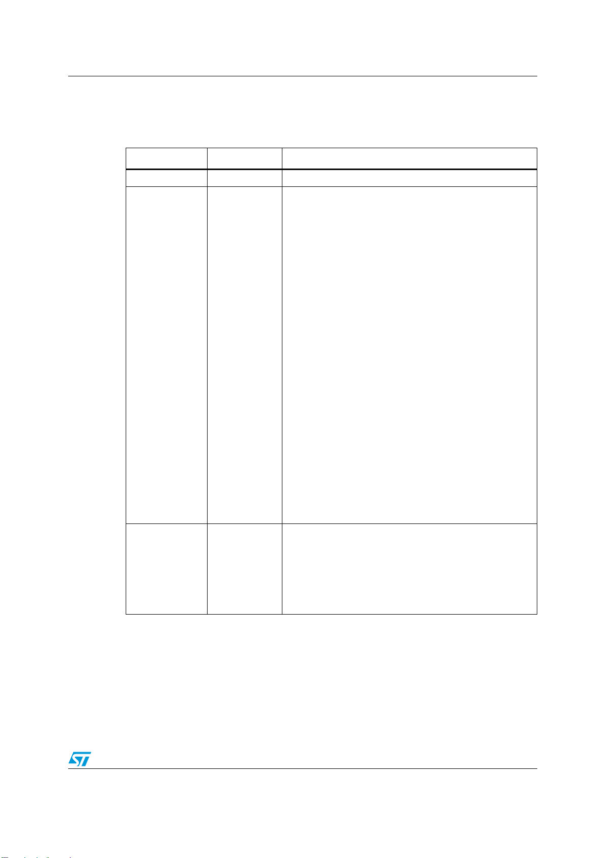
STM32F050xx Revision history
9 Revision history
Table 68. Document revision history
Date Revision Changes
25-Apr-2012 1 Initial release
Features reorganized and Section 3: Functional overview
structure changed.
Added LQFP32 package.
Changed number of GPIOs in Table 2: STM32F050xx family
device features and peripheral counts.
Updated Section 3.4: Cyclic redundancy check calculation
unit (CRC).
Modified number of priority levels in Section 3.9.1: Nested
vectored interrupt controller (NVIC).
Added footnote 3. to Table 8: Pin definitions.
Changed TIM2_CH_ETR into TIM2_CH1_ETR in Ta bl e 8 : P i n
definitions and Table 9: Alternate functions selected through
GPIOA_AFR registers for port A.
, I
03-Aug-2012 2
Updated I
VDD
VSS
, and I
characteristics .
Updated ACC
in Table 33: HSI oscillator characteristics
HSI
and Table 35: LSI oscillator characteristics.
Updated Table 44: I/O current injection susceptibility.
Added BOOT0 input low and high level voltage and updated
Rpd and Rpdu values in Table 45: I/O static characteristics.
Updated Rpdu value in Table 48: NRST pin characteristics.
Modified number of pins in V
changed condition for V
OLFM+
characteristics.
Changed V
DD
to V
in Figure 24: Typical connection
DDA
diagram using the ADC.
Updated Ts_temp in Table 52: TS characteristics.
in Table 13: Current
INJ(PIN)
and VOH description, and
OL
in Table 46: Output voltage
25-Sep-2012 3
Added packages TSSOP20 and UFQFPN28.
Replaced IWWDG with IWDG in Figure 1: Block diagram.
Replaced V
DD
with V
DDA
and V
RERINT
with V
REFINT
in
Table 19: Embedded internal reference voltage.
Replaced I
DD)
with I
in Table 33: HSI oscillator
DDA
characteristics, Table 34: HSI14 oscillator characteristics and
Table 35: LSI oscillator characteristics.
Doc ID 023079 Rev 3 97/98
Page 98

STM32F050xx
Please Read Carefully:
Information in this document is provided solely in connection with ST products. STMicroelectronics NV and its subsidiaries (“ST”) reserve the
right to make changes, corrections, modifications or improvements, to this document, and the products and services described herein at any
time, without notice.
All ST products are sold pursuant to ST’s terms and conditions of sale.
Purchasers are solely responsible for the choice, selection and use of the ST products and services described herein, and ST assumes no
liability whatsoever relating to the choice, selection or use of the ST products and services described herein.
No license, express or implied, by estoppel or otherwise, to any intellectual property rights is granted under this document. If any part of this
document refers to any third party products or services it shall not be deemed a license grant by ST for the use of such third party products
or services, or any intellectual property contained therein or considered as a warranty covering the use in any manner whatsoever of such
third party products or services or any intellectual property contained therein.
UNLESS OTHERWISE SET FORTH IN ST’S TERMS AND CONDITIONS OF SALE ST DISCLAIMS ANY EXPRESS OR IMPLIED
WARRANTY WITH RESPECT TO THE USE AND/OR SALE OF ST PRODUCTS INCLUDING WITHOUT LIMITATION IMPLIED
WARRANTIES OF MERCHANTABILITY, FITNESS FOR A PARTICULAR PURPOSE (AND THEIR EQUIVALENTS UNDER THE LAWS
OF ANY JURISDICTION), OR INFRINGEMENT OF ANY PATENT, COPYRIGHT OR OTHER INTELLECTUAL PROPERTY RIGHT.
UNLESS EXPRESSLY APPROVED IN WRITING BY TWO AUTHORIZED ST REPRESENTATIVES, ST PRODUCTS ARE NOT
RECOMMENDED, AUTHORIZED OR WARRANTED FOR USE IN MILITARY, AIR CRAFT, SPACE, LIFE SAVING, OR LIFE SUSTAINING
APPLICATIONS, NOR IN PRODUCTS OR SYSTEMS WHERE FAILURE OR MALFUNCTION MAY RESULT IN PERSONAL INJURY,
DEATH, OR SEVERE PROPERTY OR ENVIRONMENTAL DAMAGE. ST PRODUCTS WHICH ARE NOT SPECIFIED AS "AUTOMOTIVE
GRADE" MAY ONLY BE USED IN AUTOMOTIVE APPLICATIONS AT USER’S OWN RISK.
Resale of ST products with provisions different from the statements and/or technical features set forth in this document shall immediately void
any warranty granted by ST for the ST product or service described herein and shall not create or extend in any manner whatsoever, any
liability of ST.
ST and the ST logo are trademarks or registered trademarks of ST in various countries.
Information in this document supersedes and replaces all information previously supplied.
The ST logo is a registered trademark of STMicroelectronics. All other names are the property of their respective owners.
© 2012 STMicroelectronics - All rights reserved
STMicroelectronics group of companies
Australia - Belgium - Brazil - Canada - China - Czech Republic - Finland - France - Germany - Hong Kong - India - Israel - Italy - Japan -
Malaysia - Malta - Morocco - Philippines - Singapore - Spain - Sweden - Switzerland - United Kingdom - United States of America
www.st.com
98/98 Doc ID 023079 Rev 3
 Loading...