

Datasheet STM32F030F4, STM32F030C6, STM32F030K6, STM32F030C8, STM32F030R8 Datasheet (STMicroelectronics)
...Page 1

STM32F030x4/x6/x8/xC
Errata sheet
STM32F030x4/x6/x8/xC device errata
Applicability
This document applies to the part numbers of STM32F030x4/x6/x8/xC devices and the device variants as stated in this page.
It gives a summary and a description of the device errata, with respect to the device datasheet and reference manual RM0360.
Deviation of the real device behavior from the intended device behavior is considered to be a device limitation. Deviation of the
description in the reference manual or the datasheet from the intended device behavior is considered to be a documentation
erratum. The term “errata” applies both to limitations and documentation errata.
Table 1. Device summary
Reference Part numbers
STM32F030x4 STM32F030F4
STM32F030x6 STM32F030C6, STM32F030K6
STM32F030x8 STM32F030C8, STM32F030R8
STM32F030xC STM32F030CC, STM32F030RC
Table 2. Device variants
Reference
STM32F030x4
STM32F030x6 A or 1 0x1000
STM32F030x8 B, 1, or 2 0x2000
STM32F030xC A 0x1000
1. Refer to the device datasheet for how to identify this code on different types of package.
2. REV_ID[15:0] bitfield of DBGMCU_IDCODE register.
Device marking
A or 1 0x1000
Silicon revision codes
(1)
REV_ID
(2)
ES0219 - Rev 5 - October 2020
For further information contact your local STMicroelectronics sales office.
www.st.com
Page 2

1 Summary of device errata
The following table gives a quick reference to the STM32F030x4/x6/x8/xC device limitations and their status:
A = limitation present, workaround available
N = limitation present, no workaround available
P = limitation present, partial workaround available
“-” = limitation absent
Applicability of a workaround may depend on specific conditions of target application. Adoption of a workaround
may cause restrictions to target application. Workaround for a limitation is deemed partial if it only reduces the
rate of occurrence and/or consequences of the limitation, or if it is fully effective for only a subset of instances on
the device or in only a subset of operating modes, of the function concerned.
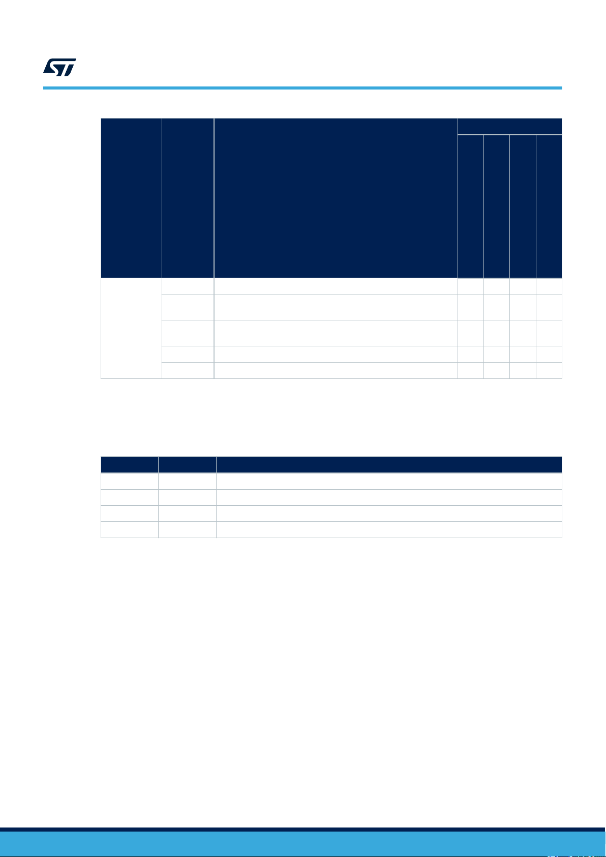
Table 3. Summary of device limitations
STM32F030x4/x6/x8/xC
Summary of device errata
Status
Function Section Limitation
System
GPIO
DMA 2.4.1
ADC
TIM
IWDG
2.2.1
2.2.2 RDP Level 1 issue P P P P
2.3.1
2.3.2
2.5.1
2.5.2
2.5.3 ADEN bit cannot be set immediately after the ADC calibration A A A A
2.6.1
2.6.3 Consecutive compare event missed in specific conditions N N N N
2.6.4 Output compare clear not working with external counter reset P P P P
2.7.1 RVU flag not reset in Stop A A A A
2.7.2 PVU flag not reset in Stop A A A A
2.7.3 WVU flag not reset in Stop A A A A
2.7.4 RVU flag not cleared at low APB clock frequency A A A A
Wakeup sequence from Standby mode when using more than
one wakeup source
Extra consumption on GPIOs PB0 / PC0 to PC5 on 20/48-pin
devices
GPIOx locking mechanism not working properly for
GPIOx_OTYPER register
DMA disable failure and error flag omission upon simultaneous
transfer error and global flag clear
ADCAL bit is not cleared when successive calibrations are
performed and system clock frequency is considerably higher
than the ADC clock frequency
Overrun flag is not set if EOC reset coincides with new
conversion end
PWM re-enabled in automatic output enable mode despite of
system break
STM32F030x4 Rev. A, 1
STM32F030x6 Rev. A, 1
STM32F030x8 Rev. B, 1, 2
A A A A
A - A -
P P P P
A A A A
A A A A
P P P P
P P P P
STM32F030xC Rev. A
ES0219 - Rev 5
page 2/29
Page 3

Function Section Limitation
STM32F030x4/x6/x8/xC
Summary of device errata
Status
IWDG
RTC and
TAMP
I2C
USART
SPI
STM32F030x4 Rev. A, 1
STM32F030x6 Rev. A, 1
STM32F030x8 Rev. B, 1, 2
2.7.5 PVU flag not cleared at low APB clock frequency
2.7.6 WVU flag not cleared at low APB clock frequency A A A A
2.8.1 Spurious tamper detection when disabling the tamper channel N N N N
2.8.2 RTC calendar registers are not locked properly A A A A
2.8.3 RTC interrupt can be masked by another RTC interrupt A A A A
2.8.4
2.8.5
2.8.6 A tamper event preceding the tamper detect enable not detected A A A A
2.9.1
2.9.2
2.9.3
2.9.5
2.9.6 Spurious bus error detection in master mode A A A A
2.9.7 Last-received byte loss in reload mode P P P P
2.9.8 Spurious master transfer upon own slave address match P P P P
2.9.9 OVR flag not set in underrun condition N N N N
2.9.10 Transmission stalled after first byte transfer A A A A
2.10.1
2.10.2
2.10.3
2.10.4 Break request preventing TC flag from being set A A A A
2.10.5 RTS is active while RE = 0 or UE = 0 A A A A
2.10.6 Receiver timeout counter wrong start in two-stop-bit configuration - - - A
2.10.7 Anticipated end-of-transmission signaling in SPI slave mode A A A A
2.10.8 Data corruption due to noisy receive line N N N N
2.11.1 BSY bit may stay high when SPI is disabled A A A A
Calendar initialization may fail in case of consecutive INIT mode
entry
Alarm flag may be repeatedly set when the core is stopped in
debug
10-bit slave mode: wrong direction bit value upon Read header
receipt
10-bit combined with 7-bit slave mode: ADDCODE may indicate
wrong slave address detection
10-bit master mode: new transfer cannot be launched if first part
of the address is not acknowledged by the slave
Wrong data sampling when data setup time (tSU;DAT) is shorter
than one I2C kernel clock period
Consistency not checked in mode 1 of automatic baud rate
detection
Framing error (FE) flag low upon automatic baud rate detection
error
Last byte written in TDR might not be transmitted if TE is cleared
just after writing in TDR
A A A A
A A A A
N N N N
A A A -
N N N -
A A A A
P P P P
N N N -
A A A -
A A A A
STM32F030xC Rev. A
ES0219 - Rev 5
page 3/29
Page 4
Function Section Limitation
STM32F030x4/x6/x8/xC
Summary of device errata
Status
2.11.2 BSY bit may stay high at the end of data transfer in slave mode
Corrupted last bit of data and/or CRC, received in master mode
with delayed SCK feedback
SPI CRC corruption upon DMA transaction completion by another
peripheral
SPI
2.11.3
2.11.4
2.11.5 Packing mode limitation at reception P P P -
2.11.7 Data flow corruption in master receiver TI half-duplex mode P P P -
The following table gives a quick reference to the documentation errata.
Table 4. Summary of device documentation errata
Function
DMA 2.4.2 Byte and half-word accesses not supported
TIM 2.6.2 TRGO and TRGO2 trigger output failure
I2C 2.9.4 Wrong behavior in Stop mode
SPI 2.11.6 CRC error in SPI slave mode if internal NSS changes before CRC transfer
Section Documentation erratum
STM32F030x4 Rev. A, 1
STM32F030x6 Rev. A, 1
STM32F030x8 Rev. B, 1, 2
A A A A
A A A -
P P P -
STM32F030xC Rev. A
ES0219 - Rev 5
page 4/29
Page 5

STM32F030x4/x6/x8/xC
Description of device errata
2 Description of device errata
The following sections describe limitations of the applicable devices with Arm® core and provide workarounds if
available. They are grouped by device functions.
Note: Arm is a registered trademark of Arm Limited (or its subsidiaries) in the US and/or elsewhere.
2.1 Core
Reference manual and errata notice for the Arm® Cortex®-M0 core revision r0p0 is available from http://
infocenter.arm.com.
2.2 System
2.2.1 Wakeup sequence from Standby mode when using more than one wakeup source
Description
The various wakeup sources are logically OR-ed in front of the rising-edge detector that generates the wakeup
flag (WUF). The WUF needs to be cleared prior to Standby mode entry, otherwise the MCU wakes up
immediately.
If one of the configured wakeup sources is kept high during the clearing of the WUF (by setting the CWUF bit), it
may mask further wakeup events on the input of the edge detector. As a consequence, the MCU might not be
able to wake up from Standby mode.
Workaround
Apply the following sequence before entering Standby mode:
1. Disable all used wakeup sources
2. Clear all related wakeup flags
3. Re-enable all used wakeup sources
4. Enter Standby mode
Note: Be aware that, when applying this workaround, if one of the wakeup sources is still kept high, the MCU enters
Standby mode but then it wakes up immediately, generating a power reset.
2.2.2 RDP Level 1 issue
Description
When the RDP Level 1 protection is set, there exists a logic issue that compromises protection of the Flash
memory against debugger access. When the debugger is connected to the device, the first transaction with the
Flash memory after a power on reset/power up is granted because of a race condition existing between this
debugger access and the protection mechanism of the Flash memory. As a result, the debugger may access one
data in the Flash memory after power up.
ES0219 - Rev 5
Workaround
For customers concerned by the confidentiality of their firmware, it is recommended to use the RDP Level 2
protection.
page 5/29
Page 6

STM32F030x4/x6/x8/xC
2.3 GPIO
2.3.1 Extra consumption on GPIOs PB0 / PC0 to PC5 on 20/48-pin devices
Description
For lower pin count devices, some GPIOs are not available on the package. The hardware forces them to safe
configuration.
In this situation, software reconfiguration of PB0 (on STM32F030F4) and PC0 to PC5 (on STM32F030C8) to
analog mode opens a path between V
can be observed if V
Workaround
Do not reconfigure PB0 (on STM32F030F4) and PC0 to PC5 (on STM32F030C8) GPIOs to analog mode on
20/48-pin devices.
is higher than V
DDA
2.3.2 GPIOx locking mechanism not working properly for GPIOx_OTYPER register
Description
DDA
and V
DDIO
. Additional current consumption in the range of tens of μA
DDIO
.
GPIO
Locking GPIOx_OTYPER[i] with i = 15 to 8 unduly depends on GPIOx_LCKR[i-8] instead on GPIOx_LCKR[i].
GPIOx_LCKR[i-8] locks both GPIOx_OTYPER[i] and GPIOx_OTYPER[i-8]. It is not possible to lock
GPIOx_OTYPER[i] with i = 15...8 without also locking GPIOx_OTYPER[i-8].
Workaround
The only way to lock GPIOx_OTYPER[i] with i=15 to 8 is to also lock GPIOx_OTYPER[i-8].
2.4
DMA
2.4.1 DMA disable failure and error flag omission upon simultaneous transfer error and global flag
clear
Description
Upon a data transfer error in a DMA channel x, both the specific TEIFx and the global GIFx flags are raised and
the channel x is normally automatically disabled. However, if in the same clock cycle the software clears the GIFx
flag (by setting the CGIFx bit of the DMA_IFCR register), the automatic channel disable fails and the TEIFx flag is
not raised.
This issue does not occur with ST's HAL software that does not use and clear the GIFx flag when the channel is
active, but uses and clears the HTIFx, TCIFx, and TEIFx specific event flags instead.
Workaround
Do not clear GIFx flags when the channel is active. Instead, use HTIFx, TCIFx, and TEIFx specific event flags and
their corresponding clear bits.
2.4.2 Byte and half-word accesses not supported
Description
Some reference manual revisions may wrongly state that the DMA registers are byte- and half-word-accessible.
Instead, the DMA registers must always be accessed through aligned 32-bit words. Byte or half-word write
accesses cause an erroneous behavior.
ST's low-level driver and HAL software only use aligned 32-bit accesses to the DMA registers.
This is a description inaccuracy issue rather than a product limitation.
ES0219 - Rev 5
page 6/29
Page 7

STM32F030x4/x6/x8/xC
Workaround
No application workaround is required.
2.5 ADC
2.5.1 ADCAL bit is not cleared when successive calibrations are performed and system clock
frequency is considerably higher than the ADC clock frequency
Description
The ADC calibration is launched by setting ADCAL bit of ADC_CR register. It can only be initiated when the ADC
is disabled (ADEN cleared in ADC_CR register). ADCAL bit stays at 1 during the whole calibration sequence and
is cleared by hardware as soon the calibration completes.
However, when at least two calibrations are performed in a row and the system clock frequency is considerably
higher than the ADC clock, the ADCAL bit is set again after being cleared by hardware when the first calibration
phase ends. The ADCAL bit remains set, waiting for the calibration to complete and hence for a hardware clear
that never occurs since the ADC clock is stopped.
Workaround
ADC
Avoid performing successive calibrations.
2.5.2 Overrun flag is not set if EOC reset coincides with new conversion end
Description
If the EOC flag is cleared by an ADC_DR register read operation or by software during the same APB cycle in
which the data from a new conversion are written in the ADC_DR register, the overrun event duly occurs (which
results in the loss of either current or new data) but the overrun flag (OVR) may stay low.
Workaround
Clear the EOC flag, by performing an ADC_DR read operation or by software within less than one ADC
conversion cycle period from the last conversion cycle end, in order to avoid the coincidence with the end of the
new conversion cycle.
2.5.3 ADEN bit cannot be set immediately after the ADC calibration
Description
At the end of the ADC calibration, an internal reset of ADEN bit occurs four ADC clock cycles after the ADCAL bit
is cleared by hardware. As a consequence, if the ADEN bit is set within those four ADC clock cycles, it is reset
shortly after by the calibration logic and the ADC remains disabled.
Workaround
Apply one of the following measures:
• When the ADC calibration is complete (ADCAL = 0), keep setting the ADEN bit until the ADRDY flag goes
high.
• After the ADCAL is cleared, wait for a minimum of four ADC clock cycles before enabling the ADC
(ADEN = 1).
• Always perform the ADC calibration with ADC clock frequency = APB frequency / 2.
ES0219 - Rev 5
page 7/29
Page 8

STM32F030x4/x6/x8/xC
2.6 TIM
2.6.1 PWM re-enabled in automatic output enable mode despite of system break
Description
In automatic output enable mode (AOE bit set in TIMx_BDTR register), the break input can be used to do a cycleby-cycle PWM control for a current mode regulation. A break signal (typically a comparator with a current
threshold ) disables the PWM output(s) and the PWM is re-armed on the next counter period.
However, a system break (typically coming from the CSS Clock security System) is supposed to stop definitively
the PWM to avoid abnormal operation (for example with PWM frequency deviation).
In the current implementation, the timer system break input is not latched. As a consequence, a system break
indeed disables the PWM output(s) when it occurs, but PWM output(s) is (are) re-armed on the following counter
period.
Workaround
Preferably, implement control loops with the output clear enable function (OCxCE bit in the TIMx_CCMR1/CCMR2
register), leaving the use of break circuitry solely for internal and/or external fault protection (AOE bit reset).
2.6.2 TRGO and TRGO2 trigger output failure
TIM
Description
Some reference manual revisions may omit the following information.
The timers can be linked using ITRx inputs and TRGOx outputs. Additionally, the TRGOx outputs can be used as
triggers for other peripherals (for example ADC). Since this circuitry is based on pulse generation, care must be
taken when initializing master and slave peripherals or when using different master/slave clock frequencies:
• If the master timer generates a trigger output pulse on TRGOx prior to have the destination peripheral clock
enabled, the triggering system may fail.
• If the frequency of the destination peripheral is modified on-the-fly (clock prescaler modification), the
triggering system may fail.
As a conclusion, the clock of the slave timer or slave peripheral must be enabled prior to receiving events from
the master timer, and must not be changed on-the-fly while triggers are being received from the master timer.
This is a documentation issue rather than a product limitation.
Workaround
No application workaround is required or applicable as long as the application handles the clock as indicated.
2.6.3 Consecutive compare event missed in specific conditions
Description
Every match of the counter (CNT) value with the compare register (CCR) value is expected to trigger a compare
event. However, if such matches occur in two consecutive counter clock cycles (as consequence of the CCR
value change between the two cycles), the second compare event is missed for the following CCR value
changes:
in edge-aligned mode, from ARR to 0:
•
– first compare event: CNT = CCR = ARR
– second (missed) compare event: CNT = CCR = 0
•
in center-aligned mode while up-counting, from ARR-1 to ARR (possibly a new ARR value if the period is
also changed) at the crest (that is, when TIMx_RCR = 0):
– first compare event: CNT = CCR = (ARR-1)
– second (missed) compare event: CNT = CCR = ARR
ES0219 - Rev 5
page 8/29
Page 9

• in center-aligned mode while down-counting, from 1 to 0 at the valley (that is, when TIMx_RCR = 0):
– first compare event: CNT = CCR = 1
– second (missed) compare event: CNT = CCR = 0
This typically corresponds to an abrupt change of compare value aiming at creating a timer clock single-cyclewide pulse in toggle mode.
As a consequence:
• In toggle mode, the output only toggles once per counter period (squared waveform), whereas it is expected
to toggle twice within two consecutive counter cycles (and so exhibit a short pulse per counter period).
• In center mode, the compare interrupt flag does note rise and the interrupt is not generated.
Note: The timer output operates as expected in modes other than the toggle mode.
Workaround
None.
2.6.4 Output compare clear not working with external counter reset
Description
The output compare clear event (ocref_clr) is not correctly generated when the timer is configured in the following
slave modes: Reset mode, Combined reset + trigger mode, and Combined gated + reset mode.
The PWM output remains inactive during one extra PWM cycle if the following sequence occurs:
1. The output is cleared by the ocref_clr event.
2. The timer reset occurs before the programmed compare event.
STM32F030x4/x6/x8/xC
IWDG
Workaround
Apply one of the following measures:
• Use BKIN (or BKIN2 if available) input for clearing the output, selecting the Automatic output enable mode
(AOE = 1).
• Mask the timer reset during the PWM ON time to prevent it from occurring before the compare event (for
example with a spare timer compare channel open-drain output connected with the reset signal, pulling the
timer reset line down).
2.7 IWDG
2.7.1 RVU flag not reset in Stop
Description
Successful write to the IWDG_RLR register raises the RVU flag and prevents further write accesses to the
register until the RVU flag is automatically cleared by hardware. However, if the device enters Stop mode while
the RVU flag is set, the hardware never clears that flag, and writing to the IWDG_RLR register is no longer
possible.
Workaround
Ensure that the RVU flag is cleared before entering Stop mode.
2.7.2 PVU flag not reset in Stop
Description
ES0219 - Rev 5
Successful write to the IWDG_PR register raises the PVU flag and prevents further write accesses to the register
until the PVU flag is automatically cleared by hardware. However, if the device enters Stop mode while the PVU
flag is set, the hardware never clears that flag, and writing to the IWDG_PR register is no longer possible.
page 9/29
Page 10

Workaround
Ensure that the PVU flag is cleared before entering Stop mode.
2.7.3 WVU flag not reset in Stop
Description
Successful write to the IWDG_WINR register raises the WVU flag and prevents further write accesses to the
register until the WVU flag is automatically cleared by hardware. However, if the device enters Stop mode while
the WVU flag is set, the hardware never clears that flag, and writing to the IWDG_WINR register is no longer
possible.
Workaround
Ensure that the WVU flag is cleared before entering Stop mode.
2.7.4 RVU flag not cleared at low APB clock frequency
Description
Successful write to the IWDG_RLR register raises the RVU flag and prevents further write accesses to the
register until the RVU flag is automatically cleared by hardware. However, at APB clock frequency lower than
twice the IWDG clock frequency, the hardware never clears that flag, and writing to the IWDG_RLR register is no
longer possible.
STM32F030x4/x6/x8/xC
IWDG
Workaround
Set the APB clock frequency higher than twice the IWDG clock frequency.
2.7.5 PVU flag not cleared at low APB clock frequency
Description
Successful write to the IWDG_PR register raises the PVU flag and prevents further write accesses to the register
until the PVU flag is automatically cleared by hardware. However, at APB clock frequency lower than twice the
IWDG clock frequency, the hardware never clears that flag, and writing to the IWDG_PR register is no longer
possible.
Workaround
Set the APB clock frequency higher than twice the IWDG clock frequency.
2.7.6 WVU flag not cleared at low APB clock frequency
Description
Successful write to the IWDG_WINR register raises the WVU flag and prevents further write accesses to the
register until the WVU flag is automatically cleared by hardware. However, at APB clock frequency lower than
twice the IWDG clock frequency, the hardware never clears that flag, and writing to the IWDG_WINR register is
no longer possible.
Workaround
Set the APB clock frequency higher than twice the IWDG clock frequency.
ES0219 - Rev 5
page 10/29
Page 11

2.8 RTC and TAMP
2.8.1 Spurious tamper detection when disabling the tamper channel
Description
If the tamper detection is configured for detecting on the falling edge event (TAMPFLT = 00 and TAMPxTRG = 1)
and if the tamper event detection is disabled when the tamper pin is at high level, a false tamper event is
detected.
Workaround
None.
2.8.2 RTC calendar registers are not locked properly
Description
When reading the calendar registers with BYPSHAD = 0, the RTC_TR and RTC_DR registers may not be locked
after reading the RTC_SSR register. This happens if the read operation is initiated one APB clock period before
the shadow registers are updated. This can result in a non-consistency of the three registers. Similarly, the
RTC_DR register can be updated after reading the RTC_TR register instead of being locked.
STM32F030x4/x6/x8/xC
RTC and TAMP
Workaround
Apply one of the following measures:
• use BYPSHAD = 1 mode (bypass shadow registers), or
• if BYPSHAD = 0, read SSR again after reading SSR/TR/DR to confirm that SSR is still the same, otherwise
read the values again.
2.8.3 RTC interrupt can be masked by another RTC interrupt
Description
One RTC interrupt request can mask another RTC interrupt request if they share the same EXTI configurable line.
For example, interrupt requests from Alarm A and Alarm B or those from tamper and timestamp events are OR-ed
to the same EXTI line (refer to the EXTI line connections table in the Extended interrupt and event controller
(EXTI) section of the reference manual).
The following code example and figure illustrate the failure mechanism: The Alarm A event is lost (fails to
generate interrupt) as it occurs in the failure window, that is, after checking the Alarm A event flag but before the
effective clear of the EXTI interrupt flag by hardware. The effective clear of the EXTI interrupt flag is delayed with
respect to the software instruction to clear it.
Alarm interrupt service routine:
void RTC_Alarm_IRQHandler(void)
{
CLEAR_ALARM_EXTI(); /* Clear the EXTI line flag for RTC alarms*/
If(ALRAF) /* Check if Alarm A triggered ISR */
{
CLEAR_FLAG(ALRAF); /* Clear the Alarm A interrupt pending bit */
PROCESS_AlarmAEvent(); /* Process Alarm A event */
}
If(ALRBF) /* Check if Alarm B triggered ISR */
{
CLEAR_FLAG(ALRBF); /* Clear the Alarm B interrupt pending bit */
PROCESS_AlarmBEvent(); /* Process Alarm B event */
}
}
ES0219 - Rev 5
page 11/29
Page 12

Alarm B Flag
Alarm A Flag
EXTI Flag
ISR execution
Figure 1. Masked RTC interrupt
Failure window:
Alarm A Flag is being set after the software checks
its value
Alarm A Flag does not raise EXTI flag because this
one is not yet hardware cleared.
CLEAR_
ALARM_
EXTI();
If (ALRBF)
If
{
(ALRA
CLEAR_FLAG(ALRBF);
F)
PROCESS_AlarmBEvent();
}
STM32F030x4/x6/x8/xC
RTC and TAMP
Alarm A is never processed
because no interrupt is generated
through EXTI
Workaround
In the interrupt service routine, apply three consecutive event flag ckecks - source one, source two, and source
one again, as in the following code example:
void RTC_Alarm_IRQHandler(void)
{
CLEAR_ALARM_EXTI(); /* Clear the EXTI's line Flag for RTC Alarm */
If(ALRAF) /* Check if AlarmA triggered ISR */
{
CLEAR_FLAG(ALRAF); /* Clear the AlarmA interrupt pending bit */
PROCESS_AlarmAEvent(); /* Process AlarmA Event */
}
If(ALRBF) /* Check if AlarmB triggered ISR */
{
CLEAR_FLAG(ALRBF); /* Clear the AlarmB interrupt pending bit */
PROCESS_AlarmBEvent(); /* Process AlarmB Event */
}
If(ALRAF) /* Check if AlarmA triggered ISR */
{
CLEAR_FLAG(ALRAF); /* Clear the AlarmA interrupt pending bit */
PROCESS_AlarmAEvent(); /* Process AlarmA Event */
}
}
2.8.4 Calendar initialization may fail in case of consecutive INIT mode entry
Description
If the INIT bit of the RTC_ISR register is set between one and two RTCCLK cycles after being cleared, the INITF
flag is set immediately instead of waiting for synchronization delay (which should be between one and two
RTCCLK cycles), and the initialization of registers may fail.
Depending on the INIT bit clearing and setting instants versus the RTCCLK edges, it can happen that, after being
immediately set, the INITF flag is cleared during one RTCCLK period then set again. As writes to calendar
registers are ignored when INITF is low, a write during this critical period might result in the corruption of one or
more calendar registers.
ES0219 - Rev 5
Workaround
After existing the initialization mode, clear the BYPSHAD bit (if set) then wait for RSF to rise, before entering the
initialization mode again.
page 12/29
Page 13

STM32F030x4/x6/x8/xC
Note: It is recommended to write all registers in a single initialization session to avoid accumulating synchronization
delays.
2.8.5 Alarm flag may be repeatedly set when the core is stopped in debug
Description
When the core is stopped in debug mode, the clock is supplied to subsecond RTC alarm downcounter even
though the device is configured to stop the RTC in debug.
As a consequence, when the subsecond counter is used for alarm condition (the MASKSS[3:0] bitfield of the
RTC_ALRMASSR and/or RTC_ALRMBSSR register set to a non-zero value) and the alarm condition is met just
before entering a breakpoint or printf, the ALRAF and/or ALRBF flag of the RTC_SR register is repeatedly set by
hardware during the breakpoint or printf, which makes any tentative to clear the flag(s) ineffective.
Workaround
None.
2.8.6 A tamper event preceding the tamper detect enable not detected
Description
When the tamper detect is enabled, set in edge detection mode (TAMPFLT[1:0]=00), and
• set to active rising edge (TAMPxTRG=0): if the tamper input is already high (tamper event already occurred)
at the moment of enabling the tamper detection, the tamper event may not be detected. The probability of
detection increases with the APB frequency.
• set to active falling edge (TAMPxTRG=1): if the tamper input is already low (tamper event already occurred)
at the moment of enabling the tamper detection, the tamper event is not detected.
I2C
Workaround
The I/O state should be checked by software in the GPIO registers after enabling the tamper detection, in order to
ensure that no active edge occurred before enabling the tamper event detection.
2.9 I2C
2.9.1 10-bit slave mode: wrong direction bit value upon Read header receipt
Description
Under specific conditions, the transfer direction bit DIR (bit 16 of status register I2C_ISR) remains low upon
receipt of 10-bit addressing Read header, while normally it should be set high. Nevertheless, I2C operates
correctly in slave transmission mode, and data can be sent using the TXIS flag.
The failure described occurs when the following conditions are all met:
• I2C is configured in 10-bit addressing mode (OA1MODE is set in the I2C_OAR1 register).
• High LSBs of the slave address are equal to the 10-bit addressing Read header value (that is, OA1[7:3] =
11110, OA1[2] = OA1[9], OA1[1] = OA1[8], and OA1[0] = 1, in the I2C_OAR1 register).
• I2C receives 10-bit addressing Read header (0X 1111 0XX1) after repeated START condition, to enter slave
transmission mode.
Workaround
Avoid using the following 10-bit slave addresses:
• OA1[9:0] = 0011110001
• OA1[9:0] = 0111110011
• OA1[9:0] = 1011110101
• OA1[9:0] = 1111110111
If the use of one of these slave addresses cannot be avoided, do not use the DIR bit in the firmware.
ES0219 - Rev 5
page 13/29
Page 14

STM32F030x4/x6/x8/xC
I2C
2.9.2 10-bit combined with 7-bit slave mode: ADDCODE may indicate wrong slave address detection
Description
Under specific conditions, the ADDCODE (address match code) bitfield in the I2C_ISR register indicates a wrong
slave address.
The failure occurs when the following conditions are all met:
• A 10-bit slave address OA1 is enabled (OA1EN = 1 and OA1MODE = 1).
• A 7-bit slave address OA2 is enabled (OA2EN = 1) and it matches the non-masked bits of OA1[7:1], that is,
one of the following configurations is set:
– OA2EN = 1 and OA2MSK = 0 and OA1[7:1] = OA2[7:1]
– OA2EN = 1 and OA2MSK = 1 and OA1[7:2] = OA2[7:2]
– OA2EN = 1 and OA2MSK = 2 and OA1[7:3] = OA2[7:3]
– OA2EN = 1 and OA2MSK = 3 and OA1[7:4] = OA2[7:4]
– OA2EN = 1 and OA2MSK = 4 and OA1[7:5] = OA2[7:5]
– OA2EN = 1 and OA2MSK = 5 and OA1[7:6] = OA2[7:6]
– OA2EN = 1 and OA2MSK = 6 and OA1[7] = OA2[7]
– OA2EN = 1 and OA2MSK = 7
– GCEN = 1 and OA1[7:1] = 0000000
– ALERTEN = 1 and OA1[7:1] = 0001100
– SMBDEN = 1 and OA1[7:1] = 1100001
– SMBHEN = 1 and OA1[7:1] = 0001000
• The MCU is addressed by a bus master with its 10-bit slave address OA1.
Upon the address receipt, the ADDCODE value is OA1[7:1] equal to the 7-bit slave address, instead of 0b11110 &
OA1[9:8].
Workaround
None. If several slave addresses are enabled, mixing 10-bit and 7-bit addresses, the OA1 [7:1] part of the 10-bit
slave address must be different than the 7-bit slave address.
2.9.3 10-bit master mode: new transfer cannot be launched if first part of the address is not
acknowledged by the slave
Description
An I2C-bus master generates STOP condition upon non-acknowledge of I2C address that it sends. This applies to
7-bit address as well as to each byte of 10-bit address.
When the MCU set as I2C-bus master transmits a 10-bit address of which the first byte (5-bit header + 2 MSBs of
the address + direction bit) is not acknowledged, the MCU duly generates STOP condition but it then cannot start
any new I2C-bus transfer. In this spurious state, the NACKF flag of the I2C_ISR register and the START bit of the
I2C_CR2 register are both set, while the START bit should normally be cleared.
Workaround
In 10-bit-address master mode, if both NACKF flag and START bit get simultaneously set, proceed as follows:
1. Wait for the STOP condition detection (STOPF = 1 in I2C_ISR register).
2. Disable the I2C peripheral.
3. Wait for a minimum of three APB cycles.
4. Enable the I2C peripheral again.
ES0219 - Rev 5
page 14/29
Page 15

2.9.4 Wrong behavior in Stop mode
Description
The correct use of the I2C peripheral is to disable it (PE = 0) before entering Stop mode, and re-enable it when
back in Run mode.
Some reference manual revisions may omit this information.
Failure to respect the above while the MCU operating as slave or as master in multi-master topology enters Stop
mode during a transfer ongoing on the I2C-bus may lead to the following:
1. BUSY flag is wrongly set when the MCU exits Stop mode. This prevents from initiating a transfer in master
mode, as the START condition cannot be sent when BUSY is set.
2. If clock stretching is enabled (NOSTRETCH = 0), the SCL line is pulled low by I2C and the transfer stalled
as long as the MCU remains in Stop mode.
The occurrence of such condition depends on the timing configuration, peripheral clock frequency, and I2Cbus frequency.
This is a description inaccuracy issue rather than a product limitation.
Workaround
No application workaround is required.
STM32F030x4/x6/x8/xC
I2C
2.9.5 Wrong data sampling when data setup time (t
Description
The I2C-bus specification and user manual specify a minimum data setup time (t
• 250 ns in Standard mode
• 100 ns in Fast mode
• 50 ns in Fast mode Plus
The device does not correctly sample the I2C-bus SDA line when t
(I2C-bus peripheral clock) period: the previous SDA value is sampled instead of the current one. This can result in
a wrong receipt of slave address, data byte, or acknowledge bit.
Workaround
Increase the I2C kernel clock frequency to get I2C kernel clock period within the transmitter minimum data setup
time. Alternatively, increase transmitter’s minimum data setup time. If the transmitter setup time minimum value
corresponds to the minimum value provided in the I2C-bus standard, the minimum I2CCLK frequencies are as
follows:
• In Standard mode, if the transmitter minimum setup time is 250 ns, the I2CCLK frequency must be at least
4 MHz.
• In Fast mode, if the transmitter minimum setup time is 100 ns, the I2CCLK frequency must be at least
10 MHz.
• In Fast-mode Plus, if the transmitter minimum setup time is 50 ns, the I2CCLK frequency must be at least
20 MHz.
) is shorter than one I2C kernel clock period
SU;DAT
) as:
SU;DAT
is smaller than one I2C kernel clock
SU;DAT
2.9.6 Spurious bus error detection in master mode
Description
In master mode, a bus error can be detected spuriously, with the consequence of setting the BERR flag of the
I2C_SR register and generating bus error interrupt if such interrupt is enabled. Detection of bus error has no
effect on the I2C-bus transfer in master mode and any such transfer continues normally.
Workaround
If a bus error interrupt is generated in master mode, the BERR flag must be cleared by software. No other action
is required and the ongoing transfer can be handled normally.
ES0219 - Rev 5
page 15/29
Page 16

2.9.7 Last-received byte loss in reload mode
Description
If in master receiver mode or slave receive mode with SBC = 1 the following conditions are all met:
• I2C-bus stretching is enabled (NOSTRETCH = 0)
• RELOAD bit of the I2C_CR2 register is set
• NBYTES bitfield of the I2C_CR2 register is set to N greater than 1
• byte N is received on the I2C-bus, raising the TCR flag
• N - 1 byte is not yet read out from the data register at the instant TCR is raised,
then the SCL line is pulled low (I2C-bus clock stretching) and the transfer of the byte N from the shift register to
the data register inhibited until the byte N-1 is read and NBYTES bitfield reloaded with a new value, the latter of
which also clears the TCR flag. As a consequence, the software cannot get the byte N and use its content before
setting the new value into the NBYTES field.
For I2C instances with independent clock, the last-received data is definitively lost (never transferred from the
shift register to the data register) if the data N - 1 is read within four APB clock cycles preceding the receipt of the
last data bit of byte N and thus the TCR flag raising. Refer to the product reference manual or datasheet for the
I2C implementation table.
Workaround
STM32F030x4/x6/x8/xC
I2C
• In master mode or in slave mode with SBC = 1, use the reload mode with NBYTES = 1.
• In master receiver mode, if the number of bytes to transfer is greater than 255, do not use the reload mode.
Instead, split the transfer into sections not exceeding 255 bytes and separate them with repeated START
conditions.
• Make sure, for example through the use of DMA, that the byte N - 1 is always read before the TCR flag is
raised. Specifically for I2C instances with independent clock, make sure that it is always read earlier than
four APB clock cycles before the receipt of the last data bit of byte N and thus the TCR flag raising.
The last workaround in the list must be evaluated carefully for each application as the timing depends on factors
such as the bus speed, interrupt management, software processing latencies, and DMA channel priority.
2.9.8 Spurious master transfer upon own slave address match
Description
When the device is configured to operate at the same time as master and slave (in a multi- master I2C-bus
application), a spurious master transfer may occur under the following condition:
• Another master on the bus is in process of sending the slave address of the device (the bus is busy).
• The device initiates a master transfer by bit set before the slave address match event (the ADDR flag set in
the I2C_ISR register) occurs.
• After the ADDR flag is set:
– the device does not write I2C_CR2 before clearing the ADDR flag, or
– the device writes I2C_CR2 earlier than three I2C kernel clock cycles before clearing the ADDR flag
In these circumstances, even though the START bit is automatically cleared by the circuitry handling the ADDR
flag, the device spuriously proceeds to the master transfer as soon as the bus becomes free. The transfer
configuration depends on the content of the I2C_CR2 register when the master transfer starts. Moreover, if the
I2C_CR2 is written less than three kernel clocks before the ADDR flag is cleared, the I2C peripheral may fall into
an unpredictable state.
ES0219 - Rev 5
Workaround
Upon the address match event (ADDR flag set), apply the following sequence.
Normal mode (SBC = 0):
1. Set the ADDRCF bit.
2. Before Stop condition occurs on the bus, write I2C_CR2 with the START bit low.
page 16/29
Page 17

Slave byte control mode (SBC = 1):
1. Write I2C_CR2 with the slave transfer configuration and the START bit low.
2. Wait for longer than three I2C kernel clock cycles.
3. Set the ADDRCF bit.
4. Before Stop condition occurs on the bus, write I2C_CR2 again with its current value.
The time for the software application to write the I2C_CR2 register before the Stop condition is limited, as the
clock stretching (if enabled), is aborted when clearing the ADDR flag.
Polling the BUSY flag before requesting the master transfer is not a reliable workaround as the bus may become
busy between the BUSY flag check and the write into the I2C_CR2 register with the START bit set.
2.9.9 OVR flag not set in underrun condition
Description
In slave transmission with clock stretching disabled (NOSTRETCH = 1 in the I2C_CR1 register), an underrun
condition occurs if the current byte transmission is completed on the I2C bus, and the next data is not yet written
in the TXDATA[7:0] bitfield. In this condition, the device is expected to set the OVR flag of the I2C_ISR register
and send 0xFF on the bus.
However, if the I2C_TXDR is written within the interval between two I2C kernel clock cycles before and three APB
clock cycles after the start of the next data transmission, the OVR flag is not set, although the transmitted value is
0xFF.
STM32F030x4/x6/x8/xC
USART
Workaround
None.
2.9.10 Transmission stalled after first byte transfer
Description
When the first byte to transmit is not prepared in the TXDATA register, two bytes are required successively,
through TXIS status flag setting or through a DMA request. If the first of the two bytes is written in the I2C_TXDR
register in less than two I2C kernel clock cycles after the TXIS/DMA request, and the ratio between APB clock
and I2C kernel clock frequencies is between 1.5 and 3, the second byte written in the I2C_TXDR is not internally
detected. This causes a state in which the I2C peripheral is stalled in master mode or in slave mode, with clock
stretching enabled (NOSTRETCH = 0). This state can only be released by disabling the peripheral (PE = 0) or by
resetting it.
Workaround
Apply one of the following measures:
• Write the first data in I2C_TXDR before the transmission starts.
• Set the APB clock frequency so that its ratio with respect to the I2C kernel clock frequency is lower than 1.5
or higher than 3.
2.10 USART
2.10.1 Consistency not checked in mode 1 of automatic baud rate detection
ES0219 - Rev 5
Description
In mode 1 (ABRMOD = 01) of automatic baud rate detection, the Start bit then the first data bit duration is
measured. If either single value measured is within an allowed range, the baud rate detection ends with success,
even if the two values are inconsistent. As a consequence, the automatic baud rate detection result in mode 1 is
reliable with regular input frames but not with abnormal frames.
Workaround
None.
page 17/29
Page 18

STM32F030x4/x6/x8/xC
2.10.2 Framing error (FE) flag low upon automatic baud rate detection error
Description
When the ABRE flag is set to indicate an error of automatic baud rate detection, the framing error flag FE remains
low although it should go high.
Workaround
Poll exclusively the ABRE flag when checking for automatic baud rate error.
2.10.3 Last byte written in TDR might not be transmitted if TE is cleared just after writing in TDR
Description
If the USART clock source is slow (for example LSE) and TE bit is cleared immediately after the last write to TDR,
the last byte will probably not be transmitted.
Workaround
Apply one of the following measures:
• Wait until TXE flag is set before clearing TE bit.
• Wait until TC flag is set before clearing TE bit.
USART
2.10.4 Break request preventing TC flag from being set
Description
After the end of transmission of data (D1), the transmission complete (TC) flag is not set when the following
condition is met:
• CTS hardware flow control is enabled
• D1 transmission is in progress
• D1 transmission is in progress
• D1 transmission is in progress
As a consequence, an application relying on the TC flag fails to detect the end of data transfer.
Workaround
In the application, only allow break request after the TC flag is set.
2.10.5 RTS is active while RE = 0 or UE = 0
Description
The RTS line is driven low as soon as RTSE bit is set, even if the USART is disabled (UE = 0) or the receiver is
disabled (RE = 0), that is, not ready to receive data.
Workaround
Upon setting the UE and RE bits, configure the I/O used for RTS into alternate function.
2.10.6 Receiver timeout counter wrong start in two-stop-bit configuration
Description
In two-stop-bit configuration, the receiver timeout counter starts counting from the end of the second stop bit of
the last character instead of starting from the end of the first stop bit.
Workaround
Subtract one bit duration from the value in the RTO bitfield of the USARTx_RTOR register.
ES0219 - Rev 5
page 18/29
Page 19

2.10.7 Anticipated end-of-transmission signaling in SPI slave mode
Description
In SPI slave mode, at low USART baud rate with respect to the USART kernel and APB clock frequencies, the
transmission complete flag TC of the USARTx_ISR register may unduly be set before the last bit is shifted on the
transmit line.
This leads to data corruption if, based on this anticipated end-of-transmission signaling, the application disables
the peripheral before the last bit is transmitted.
Workaround
Upon the TC flag rise, wait until the clock line remains idle for more than the half of the communication clock
cycle. Then only consider the transmission as ended.
2.10.8 Data corruption due to noisy receive line
Description
In UART mode with oversampling by 8 or 16 and with 1 or 2 stop bits, the received data may be corrupted if a
glitch to zero shorter than the half-bit occurs on the receive line within the second half of the stop bit.
Workaround
STM32F030x4/x6/x8/xC
SPI
None.
2.11
SPI
2.11.1 BSY bit may stay high when SPI is disabled
Description
The BSY flag may remain high upon disabling the SPI while operating in:
• master transmit mode and the TXE flag is low (data register full).
• master receive-only mode (simplex receive or half-duplex bidirectional receive phase) and an SCK strobing
edge has not occurred since the transition of the RXNE flag from low to high.
• slave mode and NSS signal is removed during the communication.
Workaround
When the SPI operates in:
• master transmit mode, disable the SPI when TXE = 1 and BSY = 0.
• master receive-only mode, ignore the BSY flag.
• slave mode, do not remove the NSS signal during the communication.
2.11.2 BSY bit may stay high at the end of data transfer in slave mode
Description
BSY flag may sporadically remain high at the end of a data transfer in slave mode. This occurs upon coincidence
of internal CPU clock and external SCK clock provided by master.
In such an event, if the software only relies on BSY flag to detect the end of SPI slave data transaction (for
example to enter low-power mode or to change data line direction in half-duplex bidirectional mode), the detection
fails.
As a conclusion, the BSY flag is unreliable for detecting the end of data transactions.
ES0219 - Rev 5
Workaround
Depending on SPI operating mode, use the following means for detecting the end of transaction:
• When NSS hardware management is applied and NSS signal is provided by master, use NSS flag.
page 19/29
Page 20

STM32F030x4/x6/x8/xC
• In SPI receiving mode, use the corresponding RXNE event flag.
• In SPI transmit-only mode, use the BSY flag in conjunction with a timeout expiry event. Set the timeout such
as to exceed the expected duration of the last data frame and start it upon TXE event that occurs with the
second bit of the last data frame. The end of the transaction corresponds to either the BSY flag becoming
low or the timeout expiry, whichever happens first.
Prefer one of the first two measures to the third as they are simpler and less constraining.
Alternatively, apply the following sequence to ensure reliable operation of the BSY flag in SPI transmit mode:
1. Write last data to data register.
2. Poll the TXE flag until it becomes high, which occurs with the second bit of the data frame transfer.
3. Disable SPI by clearing the SPE bit mandatorily before the end of the frame transfer.
4. Poll the BSY bit until it becomes low, which signals the end of transfer.
Note: The alternative method can only be used with relatively fast CPU speeds versus relatively slow SPI clocks
or/and long last data frames. The faster is the software execution, the shorter can be the duration of the last data
frame.
2.11.3 Corrupted last bit of data and/or CRC, received in master mode with delayed SCK feedback
Description
In master receive transaction, the last bit of the transacted frame is not captured when signal provided by internal
feedback loop from the SCK pin exceeds a critical delay. The lastly transacted bit of the stored data then keeps
value from the previously received pattern. As a consequence, the last receive data bit may be wrong and/or the
CRCERR flag can be unduly asserted if any data under check sum and/or the CRC pattern is wrongly captured.
A delay of up to two APB clock periods can be tolerated for the internal feedback delay.
Main factors contributing to the delay increase are low VDD level, high temperature, high SCK pin capacitive load
and low SCK I/O output speed. The SPI communication speed has no impact.
The following table gives the maximum allowable APB frequency versus GPIOx_OSPEEDR output speed bitfield
setting for the SCK pin, at 30pF of capacitive load. The operation is safe up to that frequency.
SPI
Table 5. Maximum allowable APB frequency at 30 pF load
GPIOx_OSPEEDR[1:0] for SCK pin
11 (high) 48
01 (medium) 36
x0 (low) 28
Max. APB frequency
[MHz]
Workaround
The following measures can be adopted, jointly or individually:
• Decrease the APB clock speed.
• Configure the I/O pad of the SCK pin to higher speed.
2.11.4 SPI CRC corruption upon DMA transaction completion by another peripheral
Description
When the following conditions are all met:
• CRC function for the SPI is enabled
• SPI transaction managed by software (as opposed to DMA) is ongoing and CRCNEXT flag set
• another peripheral using the DMA channel on which the SPI is mapped completes a DMA transfer,
the CRCNEXT bit is unexpectedly cleared and the SPI CRC calculation may be corrupted, setting the CRC error
flag.
ES0219 - Rev 5
page 20/29
Page 21

Workaround
Ensure that the DMA channel on which the SPI is mapped is not concurrently in use by another peripheral.
2.11.5 Packing mode limitation at reception
Description
When the SPI is configured to short data frame, the use of packing mode on the reception side may result in
spurious RXNE event generating an interrupt or a DMA request. As a consequence, the FIFO pointers on the
reception FIFO become misaligned, which leads to inconsistent data read back by software.
If the packing mode is used during data reception, the FIFO reception threshold must be set to 16 bits. At that
condition, when a read operation (half-word to read two data bytes in one APB access) takes place while the
RXFIFO level is equal to 3/4 (new data byte arrives before the two first ones are read), the 16-bit read decreases
the RXFIFO level to 1/4. The RXNE flag is not cleared and a new request is pending to read back next two
packed data bytes, although the FIFO only contains half of them. Internal read and write pointers in the RXFIFO
become misaligned and the data is corrupted.
The worst case is the continuous mode without clock interruption between data transfers.
The packing runs correctly when it is applied in full-duplex master non-continuous mode, in which the SPI
peripheral always transfers an even number of data bytes, then stops the data transmission for the software to
read out all the data received from the RxFIFO while SPI bus is idle before any further data transaction. Such safe
read cannot be fully guaranteed if SCK signal is continuous, and in particular when 16-bit read from FIFO filled to
3/4 level cannot be prevented.
STM32F030x4/x6/x8/xC
SPI
Workaround
Continuous mode: none
Non-continuous mode: slow down the SPI communication clock frequency as much as required for the application
to have time to read back data such as to prevent any 16-bit RXFIFO read operation while it is filled to its critical
3/4 level.
2.11.6 CRC error in SPI slave mode if internal NSS changes before CRC transfer
Description
Some reference manual revisions may omit the information that the device operating as SPI slave must be
configured in software NSS control if the SPI master pulses the NSS (for (for example in NSS pulse mode).
Otherwise, the transition of the internal NSS signal after the CRCNEXT flag is set might result in wrong CRC
value computed by the device and, as a consequence, in a CRC error. As a consequence, the NSS pulse mode
cannot be used along with the CRC function.
This is a documentation error rather than a product limitation.
Workaround
No application workaround is required as long as the device operating as SPI slave is duly configured in software
NSS control.
2.11.7 Data flow corruption in master receiver TI half-duplex mode
Description
Normally, a specific way of disabling the SPI controller in master receiver simplex mode, while receiving the last
byte, ensures that the SPI clock stops after the receipt of the last data bit. The specific disabling sequence is
described in the reference manual.
ES0219 - Rev 5
page 21/29
Page 22

STM32F030x4/x6/x8/xC
SPI
When the following conditions are all met:
• the device operates as SPI master receiver in TI half-duplex mode (BIDIMODE = 1 and BIDIOE = 0),
• the baud rate divider is set to 2, and
• the data size is set to 4-bit or 5-bit,
then upon disabling the SPI controller, even through the recommended sequence, the SPI clock may spuriously
stop earlier than after the last data bit. As a consequence of missing SPI clock pulses, the last data is not sent by
the external slave transmitter.
When enabled back again, the master receiver operates normally, including the generation of NSS pulse to start a
new data transaction.
Workaround
Instead of applying the specific disabling sequence during the transaction of the last data to receive, only disable
the SPI controller (SPE = 0) upon the last data byte receipt is completed.
Depending on the timing, this may result in sending extra SPI clock pulses, unexpected by the SPI slave, and as
a consequence, in desynchronization between the master receiver and the slave transmitter. The workaround is
therefore only guaranteed effective with slaves that are able to re-synchronize with the master receiver when a
new data transaction, signaled with an NSS pulse, is initiated by the master receiver.
ES0219 - Rev 5
page 22/29
Page 23

Revision history
Table 6. Document revision history
Date Version Changes
30-Sep-2013 1 Initial release.
Added:
• erratum GPIOx locking mechanism not working properly for
GPIOx_OTYPER register
• STM32F030xC devices
Removed:
15-Jan-2015 2
12-Oct-2016 3
09-May-2018
4
• Appendix: Revision code on device marking as the device marking
information is now included in the product datasheet
• USART erratum Communication parameters reprogramming after ATR
in Smartcard mode when SCLK is used to clock the card
• I2C erratum Wakeup frames may not wakeup the MCU mode when
STOP mode entry follows I2C enabling
Modified erratum Wrong behavior in Stop mode.
Added errata:
• ADC: Overrun flag is not set if EOC reset coincides with new conversion
end
• ADEN bit cannot be set immediately after the ADC calibration
• RTC: Spurious tamper detection when disabling the tamper channel
• RTC calendar registers are not locked properly
• A tamper event preceding the tamper detect enable not detected
• IWDG: RVU, PVU and WVU flags are not reset in STOP mode
• RVU, PVU and WVU flags are not reset with low-frequency APB
• I2C: 10-bit master mode: new transfer cannot be launched if first part of
the address is not acknowledged by the slave
• Wrong data sampling when data setup time (tSU;DAT) is shorter than
one I2C kernel clock period
• Spurious bus error detection in master mode
• USART: Break request preventing TC flag from being set
• RTS is active while RE = 0 or UE = 0
• Receiver timeout counter wrong start in two-stop-bit configuration
• Consistency not checked in mode 1 of automatic baud rate detection
• Framing error (FE) flag low upon automatic baud rate detection error
• SPI: BSY bit may stay high when SPI is disabled
• BSY bit may stay high at the end of data transfer in slave mode
• Corrupted last bit of data and/or CRC, received in master mode with
delayed SCK feedback
• CRC error in SPI slave mode if internal NSS changes before CRC
transfer
• SPI CRC corruption upon DMA transaction completion by another
peripheral
Modified:
• Document structure
• Cover page
• SPI erratum Packing mode limitation at reception
Removed erratum Communication parameters reprogramming after ATR in
Smartcard mode when SCLK is used to clock the card
Added:
• REV_ID bitfield information on the cover page
STM32F030x4/x6/x8/xC
ES0219 - Rev 5
page 23/29
Page 24

Date Version Changes
• Table 4. Summary of device documentation errata
• information on workaround qualifiers in Section 1 Summary of device
errata
• erratum DMA disable failure and error flag omission upon simultaneous
transfer error and global flag clear
• erratum Byte and half-word accesses not supported
• erratum RTC interrupt can be masked by another RTC interrupt
• erratum Last-received byte loss in reload mode
• erratum Spurious master transfer upon own slave address match
Modified:
• minor modifications in titles and/or text of existing limitation descriptors
in I2C, SPI and USART sections
• workaround of erratum Wrong data sampling when data setup time
(tSU;DAT) is shorter than one I2C kernel clock period
• erratum Wrong behavior in Stop mode re-qualified as documentation
erratum
• document ID in the footer of all pages
• renamed introductory section on the cover page
Removed redundant SPI limitation Wrong CRC transmitted in master mode
with delay on SCK feedback, kept in previous versions for historical reasons.
Added errata:
• SYSTEM: RDP Level 1 issue
• ADC: ADCAL bit is not cleared when successive calibrations are
performed and system clock frequency is considerably higher than the
ADC clock frequency
• TIM: PWM re-enabled in automatic output enable mode despite of
system break
• TRGO and TRGO2 trigger output failure
• Consecutive compare event missed in specific conditions
• Output compare clear not working with external counter reset
• IWDG: RVU flag not reset in Stop
• PVU flag not reset in Stop
• WVU flag not reset in Stop
• RVU flag not cleared at low APB clock frequency
• PVU flag not cleared at low APB clock frequency
• WVU flag not cleared at low APB clock frequency
05-Oct-2020 5
• RTC: Calendar initialization may fail in case of consecutive INIT mode
entry
• Alarm flag may be repeatedly set when the core is stopped in debug
• I2C: Spurious bus error detection in master mode
• Spurious master transfer upon own slave address match
• OVR flag not set in underrun condition
• Transmission stalled after first byte transfer
• USART: Anticipated end-of-transmission signaling in SPI slave mode
• Data corruption due to noisy receive line
Modified errata:
• Corrupted last bit of data and/or CRC, received in master mode with
delayed SCK feedback(missing table added)
• CRC error in SPI slave mode if internal NSS changes before CRC
transfer re-qualified as documentation erratum
• Overrun flag is not set if EOC reset coincides with new conversion end:
workaround re-qualified to P
• Last-received byte loss in reload mode: workaround re-qualified to P
STM32F030x4/x6/x8/xC
ES0219 - Rev 5
page 24/29
Page 25

STM32F030x4/x6/x8/xC
Date Version Changes
Removed errata RVU, PVU and WVU flags are not reset in STOP mode and
RVU, PVU and WVU flags are not reset with low-frequency APB, as
superseded with the errata added in the IWDG section.
ES0219 - Rev 5
page 25/29
Page 26

STM32F030x4/x6/x8/xC
Contents
Contents
1 Summary of device errata..........................................................2
2 Description of device errata........................................................5
2.1 Core .........................................................................5
2.2 System .......................................................................5
2.2.1 Wakeup sequence from Standby mode when using more than one wakeup source ......5
2.2.2 RDP Level 1 issue .......................................................5
2.3 GPIO.........................................................................6
2.3.1 Extra consumption on GPIOs PB0 / PC0 to PC5 on 20/48-pin devices ................6
2.3.2 GPIOx locking mechanism not working properly for GPIOx_OTYPER register ..........6
2.4 DMA .........................................................................6
2.4.1 DMA disable failure and error flag omission upon simultaneous transfer error and global
flag clear ...............................................................6
2.4.2 Byte and half-word accesses not supported ....................................6
2.5 ADC .........................................................................7
2.5.1 ADCAL bit is not cleared when successive calibrations are performed and system clock
frequency is considerably higher than the ADC clock frequency .....................7
2.5.2 Overrun flag is not set if EOC reset coincides with new conversion end ...............7
2.5.3 ADEN bit cannot be set immediately after the ADC calibration ......................7
2.6 TIM ..........................................................................8
2.6.1 PWM re-enabled in automatic output enable mode despite of system break............8
2.6.2 TRGO and TRGO2 trigger output failure .......................................8
2.6.3 Consecutive compare event missed in specific conditions .........................8
2.6.4 Output compare clear not working with external counter reset ......................9
2.7 IWDG ........................................................................9
2.7.1 RVU flag not reset in Stop..................................................9
2.7.2 PVU flag not reset in Stop..................................................9
2.7.3 WVU flag not reset in Stop ................................................10
2.7.4 RVU flag not cleared at low APB clock frequency ...............................10
2.7.5 PVU flag not cleared at low APB clock frequency ...............................10
2.7.6 WVU flag not cleared at low APB clock frequency ..............................10
2.8 RTC and TAMP ...............................................................11
ES0219 - Rev 5
page 26/29
Page 27

STM32F030x4/x6/x8/xC
Contents
2.8.1 Spurious tamper detection when disabling the tamper channel.....................11
2.8.2 RTC calendar registers are not locked properly ................................11
2.8.3 RTC interrupt can be masked by another RTC interrupt .......................... 11
2.8.4 Calendar initialization may fail in case of consecutive INIT mode entry...............12
2.8.5 Alarm flag may be repeatedly set when the core is stopped in debug ................13
2.8.6 A tamper event preceding the tamper detect enable not detected...................13
2.9 I2C .........................................................................13
2.9.1 10-bit slave mode: wrong direction bit value upon Read header receipt ..............13
2.9.2 10-bit combined with 7-bit slave mode: ADDCODE may indicate wrong slave address
detection ..............................................................14
2.9.3 10-bit master mode: new transfer cannot be launched if first part of the address is not
acknowledged by the slave ................................................14
2.9.4 Wrong behavior in Stop mode..............................................15
2.9.5 Wrong data sampling when data setup time (t
) is shorter than one I2C kernel clock
SU;DAT
period ................................................................15
2.9.6 Spurious bus error detection in master mode ..................................15
2.9.7 Last-received byte loss in reload mode .......................................16
2.9.8 Spurious master transfer upon own slave address match .........................16
2.9.9 OVR flag not set in underrun condition .......................................17
2.9.10 Transmission stalled after first byte transfer ...................................17
2.10 USART ......................................................................17
2.10.1 Consistency not checked in mode 1 of automatic baud rate detection ...............17
2.10.2 Framing error (FE) flag low upon automatic baud rate detection error................18
2.10.3 Last byte written in TDR might not be transmitted if TE is cleared just after writing in TDR 18
2.10.4 Break request preventing TC flag from being set ...............................18
2.10.5 RTS is active while RE = 0 or UE = 0 ........................................18
2.10.6 Receiver timeout counter wrong start in two-stop-bit configuration ..................18
2.10.7 Anticipated end-of-transmission signaling in SPI slave mode ......................19
2.10.8 Data corruption due to noisy receive line......................................19
2.11 SPI .........................................................................19
2.11.1 BSY bit may stay high when SPI is disabled ...................................19
2.11.2 BSY bit may stay high at the end of data transfer in slave mode....................19
2.11.3 Corrupted last bit of data and/or CRC, received in master mode with delayed SCK feedback
.....................................................................20
ES0219 - Rev 5
page 27/29
Page 28

STM32F030x4/x6/x8/xC
Contents
2.11.4 SPI CRC corruption upon DMA transaction completion by another peripheral .........20
2.11.5 Packing mode limitation at reception.........................................21
2.11.6 CRC error in SPI slave mode if internal NSS changes before CRC transfer ...........21
2.11.7 Data flow corruption in master receiver TI half-duplex mode .......................21
Revision history .......................................................................23
ES0219 - Rev 5
page 28/29
Page 29

STM32F030x4/x6/x8/xC
IMPORTANT NOTICE – PLEASE READ CAREFULLY
STMicroelectronics NV and its subsidiaries (“ST”) reserve the right to make changes, corrections, enhancements, modifications, and improvements to ST
products and/or to this document at any time without notice. Purchasers should obtain the latest relevant information on ST products before placing orders. ST
products are sold pursuant to ST’s terms and conditions of sale in place at the time of order acknowledgement.
Purchasers are solely responsible for the choice, selection, and use of ST products and ST assumes no liability for application assistance or the design of
Purchasers’ products.
No license, express or implied, to any intellectual property right is granted by ST herein.
Resale of ST products with provisions different from the information set forth herein shall void any warranty granted by ST for such product.
ST and the ST logo are trademarks of ST. For additional information about ST trademarks, please refer to www.st.com/trademarks. All other product or service
names are the property of their respective owners.
Information in this document supersedes and replaces information previously supplied in any prior versions of this document.
© 2020 STMicroelectronics – All rights reserved
ES0219 - Rev 5
page 29/29
 Loading...