How it Works
Log In / Sign Up
Buy Points
How it Works
FAQ
Contact Us
Questions and Suggestions
Users
STMicroelectronics
Loading...
S
STEVAL-CTM008V1
STEVAL-CTM009V1
STEVAL-DPSTPFC1
STEVAL-IDB005V1
STEVAL-IHM029V1
STEVAL-IHT005V2
STEVAL-IHT008V1
STEVAL-ILL082V1
STEVAL-IPFC02V1
STEVAL-LLL002V1
STEVAL-MKI109V2
STEVAL-STWINKT1
STEVAL-STWINKT1B
STEVAL-STWINMAV1
STEVAL-STWINWFV1
STEVAL-VOICE-UI
STF13NM60N
STF20N20
STF3NK80Z
STF4NK50ZD
STF5NK100Z
STGD3NB60F
STGP3NB60F
STGW30NC60WD
STGW39NC60VD
STI13NM60N
STILE01
STIPQ3M60T-H SLLIMM
STLD41PUR
STLINK-V3MINIE
STLINK-V3SET
STLUX385A
STM32
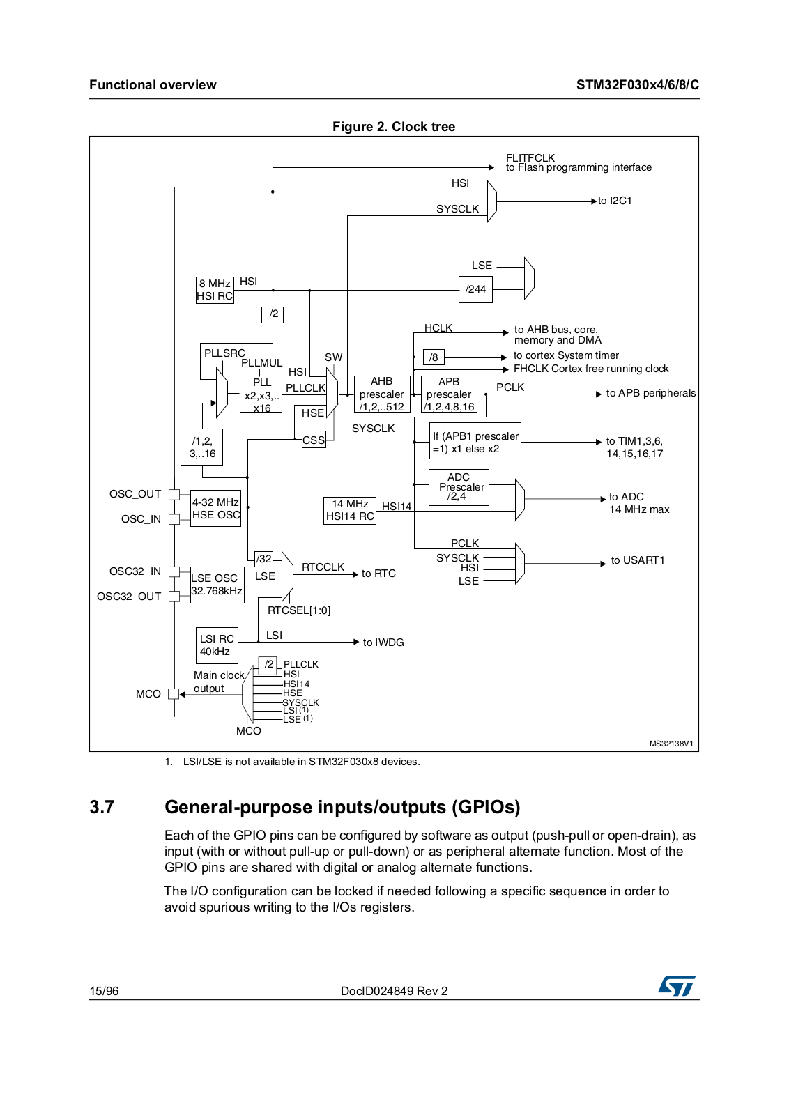
7
STM32100E-EVAL
STM32479VG
STM32479VI
STM32479ZG
STM32479ZI
STM32 Cortex-M3
STM32Cube
14
STM32Cube AWS
STM32CubeMonitor-UCPD
STM32F030C6
2
STM32F030C8
2
STM32F030CC
2
STM32F030F4
2
STM32F030K6
2
STM32F030R8
2
STM32F030RC
2
STM32F031C4
STM32F031C6
STM32F031E6
STM32F031F4
STM32F031F6
STM32F031G4
STM32F031G6
STM32F031K4
STM32F031K6
STM32F038C6
STM32F038E6
STM32F038F6
STM32F038G6
STM32F038K6
STM32F042C4
2
STM32F042C6
2
STM32F042F4
STM32F042F6
2
STM32F042G4
2
STM32F042G6
2
STM32F042K4
2
STM32F042K6
2
STM32F042T4
2
STM32F042T6
2
STM32F050C4
STM32F050C6
STM32F050F4
STM32F050F6
STM32F050G4
STM32F050G6
STM32F050K4
STM32F050K6
STM32F05 series
STM32F072CBT6
STM32F072CBU6
STM32F072RBT6
STM32F072VBT6
STM32F078CB
STM32F078RB
STM32F078VB
STM32F103C4T6A
STM32F103C6T6A
STM32F103C6U6A
STM32F103CBU6
STM32F103R4T6A
STM32 F103RCT6
STM32 F103VBT6
STM32 F407GDISC1
STM32 MPU
STM32 Series
STM32 VLDISCOV
Loading...
Loading...
Nothing found
STM32F030CC
Datasheet
29 pgs
365.9 Kb
0
Datasheet
96 pgs
1.7 Mb
0
Table of contents
Loading...
STMicroelectronics STM32F030F4, STM32F030C6, STM32F030K6, STM32F030C8, STM32F030R8 Datasheet
...
STMicroelectronics STM32F030F4, STM32F030C6, STM32F030K6, STM32F030C8, STM32F030R8, STM32F030CC, STM32F030RC Datasheet
Download
Specifications and Main Features
Frequently Asked Questions
User Manual
Download
Loading...
+
67
hidden pages
Unhide
You need points to download manuals.
1 point = 1 manual.
You can buy points or you can get point for every manual you upload.
Buy points
Upload your manuals


 Loading... Loading...