

Page 1
1 Intro
Tutorial
STM32 Cortex-M3
Author El. Ing. Lukas Kohler
Adviser Daniel Debrunner
Date 09.09.2009
Site BFH-TI Biel
Study Master of Science in Biomedical Engineering
University of Bern and University of Applied Sciences Biel
Page 2

Page 3

Abstract
The powerful STM32 controller from STMicroelectronics with integrated Cortex-M3 core has become more and more relevant in embedded applications. The key points are an excellent real-time
behavior, an outstanding power efficiency and superior peripherals.
The new developed Cortex-M3 has a high aim: A powerful processor with a uncomplex programming model which is able to replace the available 8 and 16-bit microcontroller. Tools and libraries
guarantee a short developing time and a high standardisation. A big part of written and used
software can be reused.
This manual guides you through programming an STM32F103RB microcontroller. The first chapters give an introduction to the STM32 and show how the development toolchain is set up and
used. In the main part of this documentation the peripheral is illustrated. It should lead you to
start straight ahead without reading application notes or data sheets.
I
Page 4

Page 5

Contents
1 Introduction 1
1.1 Overview of this Documentation 1
1.2 Timeline 1
1.3 Symbols used in this Document 1
1.4 License and Author 2
2 System Description 3
2.1 Introduction 3
2.2 Electrostatic Warning 3
2.3 Cortex-M3 Core 3
2.3.1 History 3
2.3.2 Cortex 4
2.4 Processor STM32F103RB from STMicroelectronics 6
2.4.1 Features 6
2.4.2 Performance Line Block Diagram 7
2.4.3 Memory Map 8
2.4.4 Interfaces 9
2.5 Development Boards 9
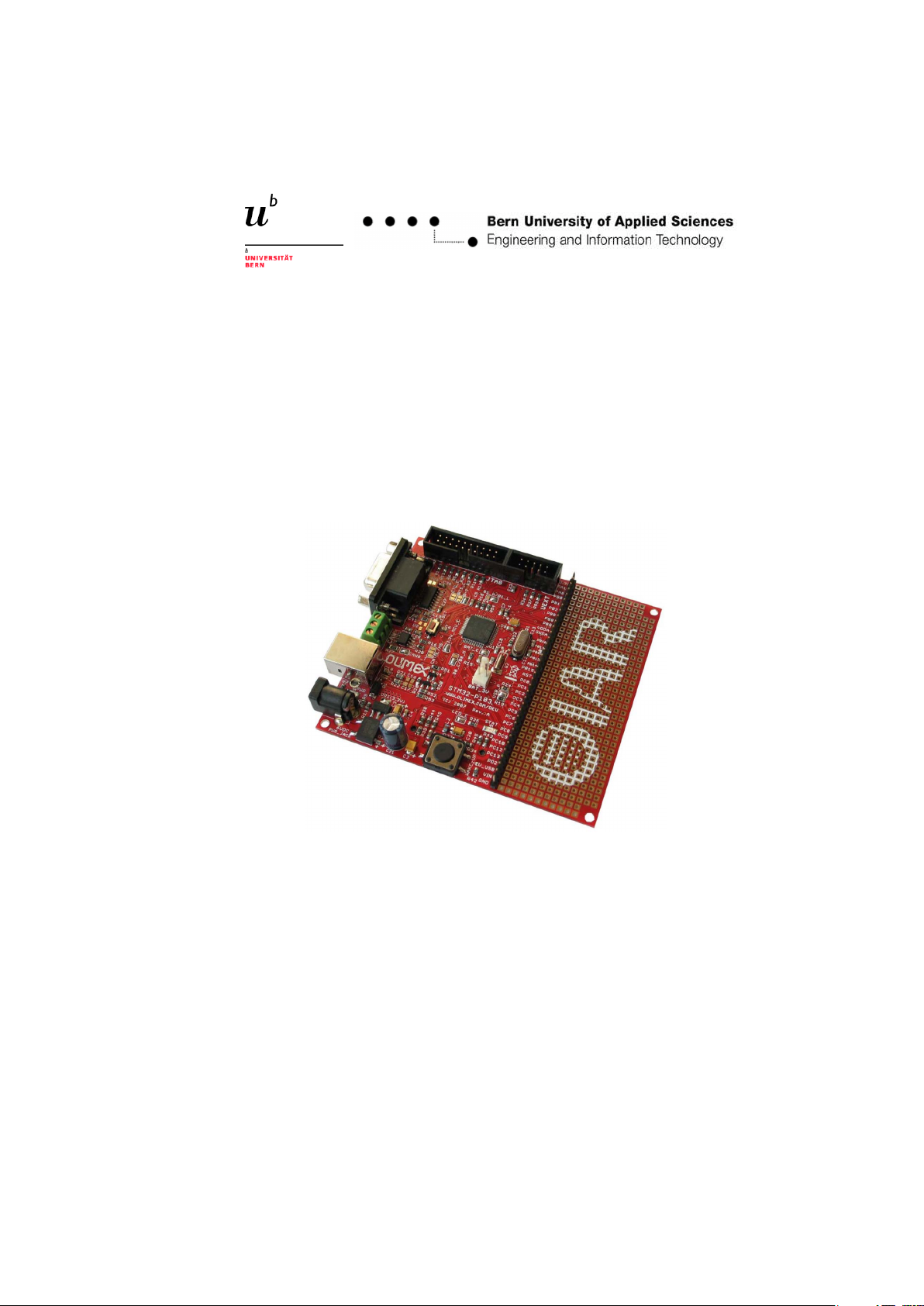
2.5.1 STM32H103 from Olimex 9
2.5.2 STM32P103 from Olimex 10
2.5.3 Setup for Developing 10
2.5.4 Board Layout and Schematic 11
2.5.5 BFH Mother Board 11
3 Keil SDK 13
3.1 Introduction 13
3.2 Install µVision3 13
3.3 Install the Driver for the JTAG Adapter 13
3.4 Install the STM32 Peripheral Library 13
3.5 Setting up a new Project 14
3.5.1 Preparation 14
3.5.2 Create a new project 14
3.5.3 Configure the Processor 15
3.5.4 Renaming the Target 16
3.6 Building 16
3.7 Simulation 17
3.7.1 Window update 18
III
Page 6

1 Intro
Contents
3.7.2 Serial Window 18
3.7.3 Performance Analyzer 18
3.8 Configuring the Target 19
3.9 Downloading 21
3.10 Debugging 21
3.11 Serial Terminal 21
3.12 Documenting Source Code 22
4 Peripherals 23
4.1 Getting Started 23
4.2 Configuration Wizard 23
4.3 Firmware Library (FWLib) 24
4.4 Register Access 25
4.5 General Purpose Input/Output (GPIO) 26
4.5.1 Configuration 26
4.5.2 Driver 27
4.5.3 Set Output 27
4.5.4 Read Input 27
4.6 Serial Interface (USART) 28
4.6.1 Ways of Operation: Polling versus Interrupts 28
4.6.2 Using Polling 28
4.6.3 Using Interrupts 29
4.6.4 Driver 29
4.6.5 Pinning 31
4.7 System Timer (SysTick) 32
4.7.1 Configuration 32
4.8 Timer (TIM) 33
4.8.1 Configuration 33
4.9 Pulse Width Modulation (PWM) 34
4.9.1 Configuration 34
4.10 External Interrupts (IRQ) 35
4.10.1 Configuration 35
4.10.2 Functionality 35
4.11 Watchdog 36
4.11.1 Configuration 36
4.12 Real Time Clock (RTC) 36
4.13 Analog to Digital Converter (ADC) 37
4.13.1 Conversion Modes 37
4.14 Controller Area Network (CAN) 40
4.14.1 CAN Analyzer 41
4.14.2 Pinning 41
4.15 Inter IC Bus (I2C) 41
4.15.1 Physical layer 42
IV STM32 Cortex-M3 Tutorial
Page 7

Contents
1 Intro
4.15.2 Communication Protocol 42
4.15.3 Pinning 44
4.16 Serial Peripheral Interface (SPI) 45
4.16.1 Physical Layer 45
4.16.2 Communication Protocol 45
4.16.3 Pinning 46
4.17 Universal Serial Bus (USB) 48
List of Figures 50
Glossary 52
Lukas Kohler V
Page 8

Page 9

1 Introduction
1.1 Overview of this Documentation
• Introduction (Chapter 1)
This chapter shows how this documentation is structured and meant to be read as well as
some project organisation.
• System Description (Chapter 2)
Here one can read all about the core Cortex-M3 and it’s implementation from STMicroelectronics into the STM32F103 processor. The development boards from Olimex as well as the
BFH mother board are presented and the interfaces shown.
• Keil SDK (Chapter 3)
This chapter shows how to set up a new project with the Keil Software Development Kit
µVision3 and how to compile, simulate, download and debug software.
• Peripherals (Chapter 4)
The biggest part of this documentation is showing how the peripherals are controlled. Example programs from using simple inputs and outputs to complex interrupts are provided.
This example based chapter shows you the way of using peripherals with simple examples.
1.2 Timeline
• Start: March 1, 2009
• Project deadline: August 30, 2009
• Presentation (BFH Biel): December 14, 2009
1.3 Symbols used in this Document
Warning: This warning should be taken seriously. Ignoring warnings could cause problems or
destroy devices.
Sample Code: Shows that a sample code exists in the directory CD:/code/ . b
Filename: hudi.c
Function: void doSomeThing()
!
1
Page 10

1 Intro
1.4 License and Author
The whole Cortex-M3 Tutorial including Source Code and Documentation by Lukas Kohler is licensed under a Creative Commons Attribution-
Noncommercial-Share Alike 3.0 United States License.
Written 2009 by Lukas Kohler k lukas.kohler@gmail.com
H 078 817 77 77
1 Introduction
2 STM32 Cortex-M3 Tutorial
Page 11

2 System Description
2.1 Introduction
This chapter describes the technical way of the development boards. Often abbreviations are used,
they are described in the glossary (Part 4.17). The microcontroller used on the different board is
always the STM32F103RB form ST with the Cortex-M3 core from ARM. The first section introduces
this core, the second the microcontroller STM32F103RB and the following the development boards
used in this document.
This chapter describes only the processor used in this document and shows the hardware setup.
The development of the software itself is described in Chapter 3.
2.2 Electrostatic Warning
Make sure that you are connected to ground before you touch any electronic circuit! Electrostatic discharges may destroy any electronic circuit.
!
2.3 Cortex-M3 Core
The target market of the Cortex-M3 core is the field that has been served by 8- or 16bit controllers.
In this market cheap but powerful controllers with little power consumption are needed.
2.3.1 History
For the last decade the ARM7 and ARM9 microcontrollers have been used as
general purpose microcontrollers. Today exist a few hundred microcontrollers
with the ARM core.
Now STMicroelectronics have launched the STM32, their first microcontroller based on the new
ARM Cortex-M3 core. This device sets new standards in performance and cost, as well as being
capable of low power operation and hard real-time control.
Currently the M3 core is licensed by 22 companies like Actel Corporation, Broadcom Corporation,
Energy Micro, Luminary Micro, NXP, STMicroelectronics, Texas Instruments, Toshiba and Zilog1.
1
Licensed M3 cores: arm.com
3
Page 12
1 Intro
2 System Description
2.3.2 Cortex
The new generation of processors comes as complete processor core that provides a standard CPU
and system architecture.
On the ARM7 systems every manufacturer had to add the basic peripherals like interrupt controller, systick timer and sleep modes. This has now been built into the Cortex-M3 core. The
Cortex-M3 provides a standardized microcontroller core which goes beyond the classical CPU to
provide the entire heart of a microcontroller (including the interrupt system, 24-bit SysTick timer,
debug system and memory map).
The Cortex family comes in three main profiles: The A profile for
high end applications (applications processors for complex OS and
user applications), R for real time and M for cost-sensitive and microcontroller applications.
The STM32 is based on the Cortex-M3 profile, which is specifically designed for high system
performance combined with low power consumption. It has a low enough cost to challenge traditional 8 and 16-bit microcontrollers.
The Cortex-M3 is a Harvard architecture (Code and Databus are separated) and has multiple buses
that allow it to perform operations in parallel. The architecture inside the Cortex-M3 is a ARMv7M RISC processor.
With only 33’000 logic cells needed to syntetisize the M3 core it is the smallest core of the ARM
family. This reduces the size of the chip and therefore cheap manufacturing processes with 0.35
µm can be used.
Interrupts
One of the key components of the Cortex-M3 core is the Nested Vector Interrupt Controller (NVIC).
The NVIC provides a standard interrupt structure for all Cortex based microcontrollers and exceptional interrupt handling. The NVIC provides dedicated interrupt vectors for up to 240 peripheral
sources where each interrupt source can be individually prioritized. The NVIC provide extremely
fast interrupt handling. The time taken from receiving an interrupt to reaching the first line of
code in your interrupt service routine is just twelve cycles.
All interrupts can be prioritized on three levels: pre-empting, sub-priority and hardware-priority.
The first two can be configured via the software and the priority can be set on 4 bits.
The interrupt service routines (ISR) can be written fully in C, therefore no Assembler is needed
any more.
Instruction Set
While the ARM7 and ARM9 CPUs have two instruction sets (the 32-bit ARM and the 16-bit
Thumb), the Cortex family is designed to support only the 16-bit Thumb-2 instruction set. The
result is a simpler assembling of the core since there is not longer need for switching between the
two instruction sets. The Thumb-2 instruction set is a rich instruction set that is designed as a
target for C/C++ compilers.
4 STM32 Cortex-M3 Tutorial
Page 13

2.3 Cortex-M3 Core
1 Intro
Cortex CPU
The heart of the Cortex core is a 32-bit RISC CPU. This CPU has a simplified version of the
ARM7/9 programmer’s model, but a richer instruction set with good integer maths support, better bit manipulation and ’harder’ real-time performance has been added.
Pipeline
The Cortex CPU can execute most instructions in a single cycle. Like the ARM7 and ARM9 CPUs
this is achieved with a three stage pipeline. Whilst one instruction is being executed, the next is
being decoded and a third is being fetched from memory.
Multiplication
A 32-bit multiplication can be done within one cycle since the Cortex-M3 offers a hardware multiplication unit.
Producer
The IP core form ARM can be implemented by different manufacturers. In this document only
the STM32F103RB from ST is described. The Core exists as well for VHDL implementation as M1
ARM 32-bit Cortex-M3 CPU only core without peripherals. The peripherals are implemented by
the manufacturers.
Power Consumption
The STM32 is a low power as well as high performance microcontroller . It can run from a 2V
supply and at 72MHz with everything switched on it consumes just 36mA. In combination with
the Cortex low power modes the STM32 has a standby power consumption of only 2µA.
Startup-Code
For the Cortex-M3 is no longer assembler startup code is needed, everything can be coded in C.
Debug-Interface
The debug interface has been changed to a scalable interface with advantages according to the
ARM7/9 family. The Cortex-M3 has a Debug Access Port (DAP) which can be used in the JTAG or
in the Serial Wire Debug Mode with only two lines (clock and data).
ARM7 processors have only a very limited amount of two Hardware-Breakpoints. In the Cortex-M3
this has been updated to 8 breakpoints. Beside the breakpoints, Fault Conditions and Exceptions
can be set. Faults and Exceptions can be supervised without the need of using breakpoints.
The debug interface works as well in the Sleep-mode.
Lukas Kohler 5
Page 14

1 Intro
2 System Description
2.4 Processor STM32F103RB from STMicroelectronics
2.4.1 Features
The STM32F103RB from STMicroelectronics is a processor with a ARM 32-bit Cortex-M3 CPU
and peripherals. STMicroelectronics is reshaping the 16/32-bit MCU market with they’r STM32
family.
The key benefits of the STM32F103RB are:
• Leading performance, real time behavior
• A lot of peripherals
• Outstanding power efficiency
• In production since 2007 7→ proved design
• 70 part numbers across 4 product lines
• SW Libraries are free available from www.st.com/mcu
• Core: CPU clock internal up to 72Mhz, single-cycle multiplication and hardware division
• Memory: 128KBytes flash, 20KByte ram and memory controller
• LCD parallel interface
• Low power states (sleep, stop and standby)
• 7 DMA channels
• RTC
• WDT
• PWM
• 3x Timers and SysTick
• Communication interface:
– 2x SPI
– 2x I2C
– 3x I2S
– 3x USART
– USB 2.0
– CAN
• Up to 51 GPIO (multiplexed with peripherals, 5V tolerable [but not for analog inputs!])
• 2x ADC 12 bit
• Operating voltage 2.0-3.6V
• Temperature: -40C +85C
• Debugging: JTAG and serial wire interface
A lot of information, data sheets and examples can be found at
http://www.st.com/mcu/familiesdocs-110.html.
6 STM32 Cortex-M3 Tutorial
Page 15
2.4 Processor STM32F103RB from STMicroelectronics
1 Intro
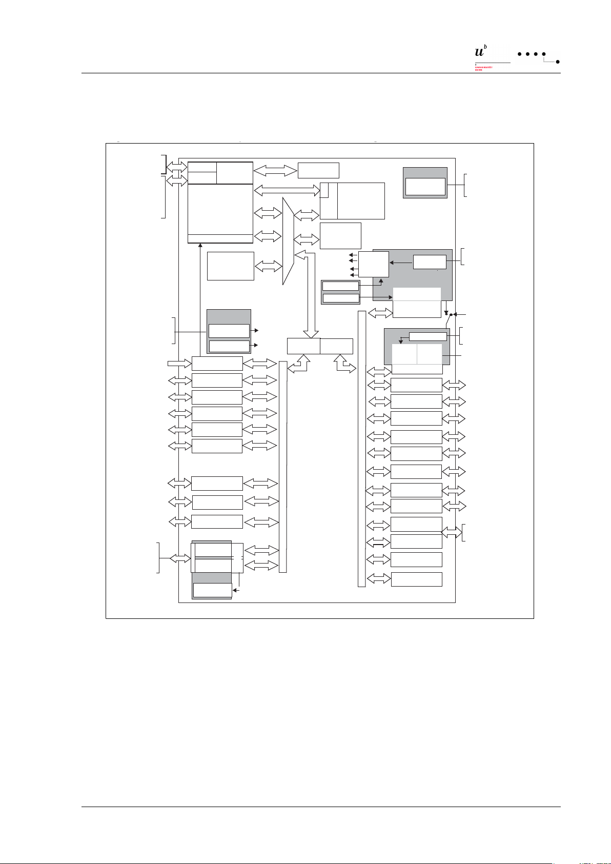
Figure 1. STM32F103xx performance line block diagram
USBDP/CA N_TX
PA[15: 0]
EXTI
WWDG
12bit ADC1
16AF
JTDI
JTCK/ SWCLK
JTMS/SWDIO
NJTRSTTRST
JTDO
NRST
V
DD
= 2 to 3.6V
80AF
PB[15: 0]
PC[15: 0]
AHB2
MOSI,MISO,SCK,NSS
SRAM
2x(8x16bit)
WAKEUP
GPIOA
GPIOB
GPIOC
F
max
: 72 M
Hz
V
SS
SCL,SDA
I2C2
V
REF+
GP DMA
TIM2
TIM3
XTAL OSC
4-16 MHz
XTAL 32 kHz
OSC_IN
OSC_OUT
OSC32_OUT
OSC32_IN
PLL &
APB1 : F
max
=24 / 36 MHz
PCLK1
HCLK
CLOCK
MANA GT
PCLK2
as AF
as AF
Flash 128 KB
VOLT. REG.
3.3V TO 1.8V
POWER
Backu p i nterf ace
as AF
TIM 4
BusM atrix
64 bit
Interface
20 KB
RTC
RC 8 MHz
Cortex-M3 CPU
Ibus
Dbus
pbu s
obl
flash
SRAM 512B
Trace
Cont rolle r
USART1
USART2
SPI2
bxCAN
7 ch annels
Back up
reg
4 Chann els
TIM1
3 com pl. Chann els
SCL,SDA ,SMBA
I2C1
as AF
RX,TX, CTS, RTS,
USART3
Temp sens or
V
REF-
PD[15: 0]
GPIOD
PE[15: 0]
GPIOE
AHB:F
max
=48/72 MHz
ETR and BKIN
4 Chann els
4 Chann els
4 Chann els
FCLK
RC 40 kHz
Stand by
IWDG
@VBAT
POR / PDR
SUPPLY
@VDDA
VDDA
VSSA
@VDDA
V
BAT
RX,TX, CTS, RTS,
Smart Card as AF
RX,TX, CTS, RTS,
CK, SmartCard as AF
APB2 : F
max
=48 / 72 MHz
NVIC
SPI1
MOSI,MISO,
SCK,NSS as AF
12bit ADC2
IF
IFIF
int erface
@VDDA
SUPERVISION
PVD
Rst
Int
@VDD
AHB2
APB2
APB 1
AWU
TAMPER-RTC
@VDD
USB 2.0 FS
USBDM/CAN_RX
System
ai14390d
TRACECLK
TRACED[0:3]
as AS
SW/JTAG
TPIU
Trace/trig
CK, SmartCard as AF
2.4.2 Performance Line Block Diagram
The block diagram in Figure 2.1 shows how the components and the core are connected together.
Lukas Kohler 7
Figure 2.1: STM32F103xx Performance Line Block Diagram
Page 16
1 Intro
2.4.3 Memory Map
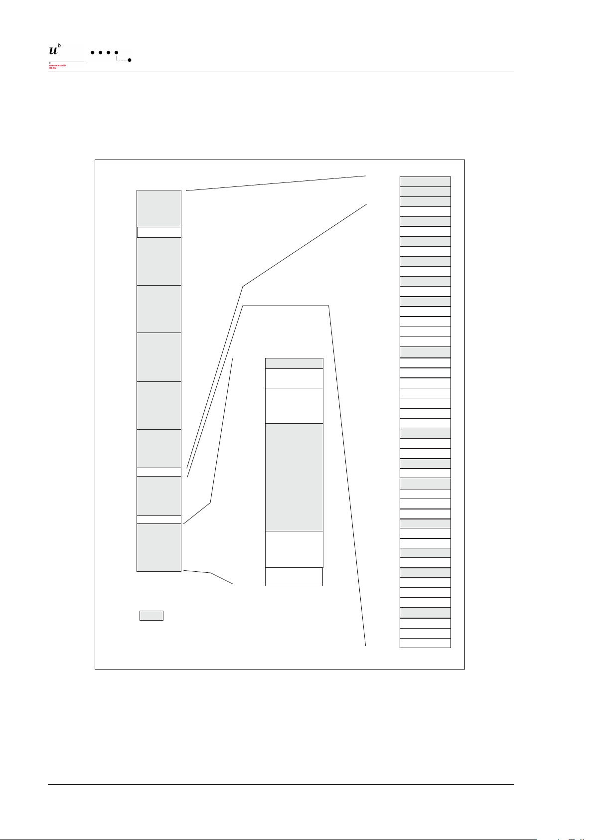
The memory map is shown in Figure 9.
Figure 9. Memory map
reserved
0x4000 0000
0x4000 0400
0x4000 0800
0x4000 0C00
0x4000 2800
0x4000 2C00
0x4000 3000
0x4000 3400
0x4000 3800
0x4000 3C00
0x4000 4400
0x4000 4800
0x4000 4C00
0x4001 0C00
0x4001 1000
0x4001 1400
0x4001 1800
0x4002 1400
APB memory space
DMA
0x4002 1000
TIM2
Reserved
0x4001 0800
0x4001 1C00
0x4001 2400
0x4001 2800
0x4001 2C00
0x4001 3000
0x4001 3400
0x4001 3800
TIM3
TIM4
reserved
RTC
WWDG
IWDG
reserved
SPI2
USART2
USART3
AFIO
Port A
Port C
Port D
reserve d
ADC1
reserved
USART1
reserved
0x4002 0400
0x4002 0000
0x4001 3C00
0x4000 5400
0x4000 5800
reserved
ADC2
TIM1
SPI1
reserved
I2C1
BKP
0x4000 6000
0x4000 5C00
Port E
PWR
Port B
I2C2
reserved
bxCAN
EXTI
reserved
RCC
reserved
Flash In terface
reserved
reserved
reserved
0x4000 6400
0x4000 6800
0x4000 6C00
0x4000 7000
0x4000 7400
0x4001 0000
0x4001 0400
0x4002 2000
0x4002 2400
0x4002 3000
0x4002 3400
0x6000 0000
0xE010 0000
reserved
0xFFFF FFFF
USB Regi sters
CRC
0
1
2
3
4
5
6
7
0x2000 0000
0x4000 0000
0x6000 0000
0x8000 0000
0xA000 0000
0xC000 0000
0xE000 0000
0xFFFF FFFF
0x0000 0000
Peripherals
SRAM
Flash memory
reserved
reserved
0x0800 0000
0x0801 FFFF
0x1FFF F000
0x1FFF FFFF
System memory
Option Bytes
0x1FFF F800
0x1FFF F80F
Cortex- M3 Internal
Perip heral s
0xE010 0000
ai14394f
shared 512 byte
USB/CAN SRAM
Aliased to Flash or system
memory depending on
BOOT pins
0x0000 0000
The memory map shows how the memory in the STM32F103RB is configured. This needs to be
known for programming the processor.
• Flash Memory: 0x0800 0000 - 0x0801 FFFF
• System Memory: 0x1FFF F000 - 0x1FFF F800
8 STM32 Cortex-M3 Tutorial
Figure 2.2: STM32F103xx memory map
2 System Description
Page 17
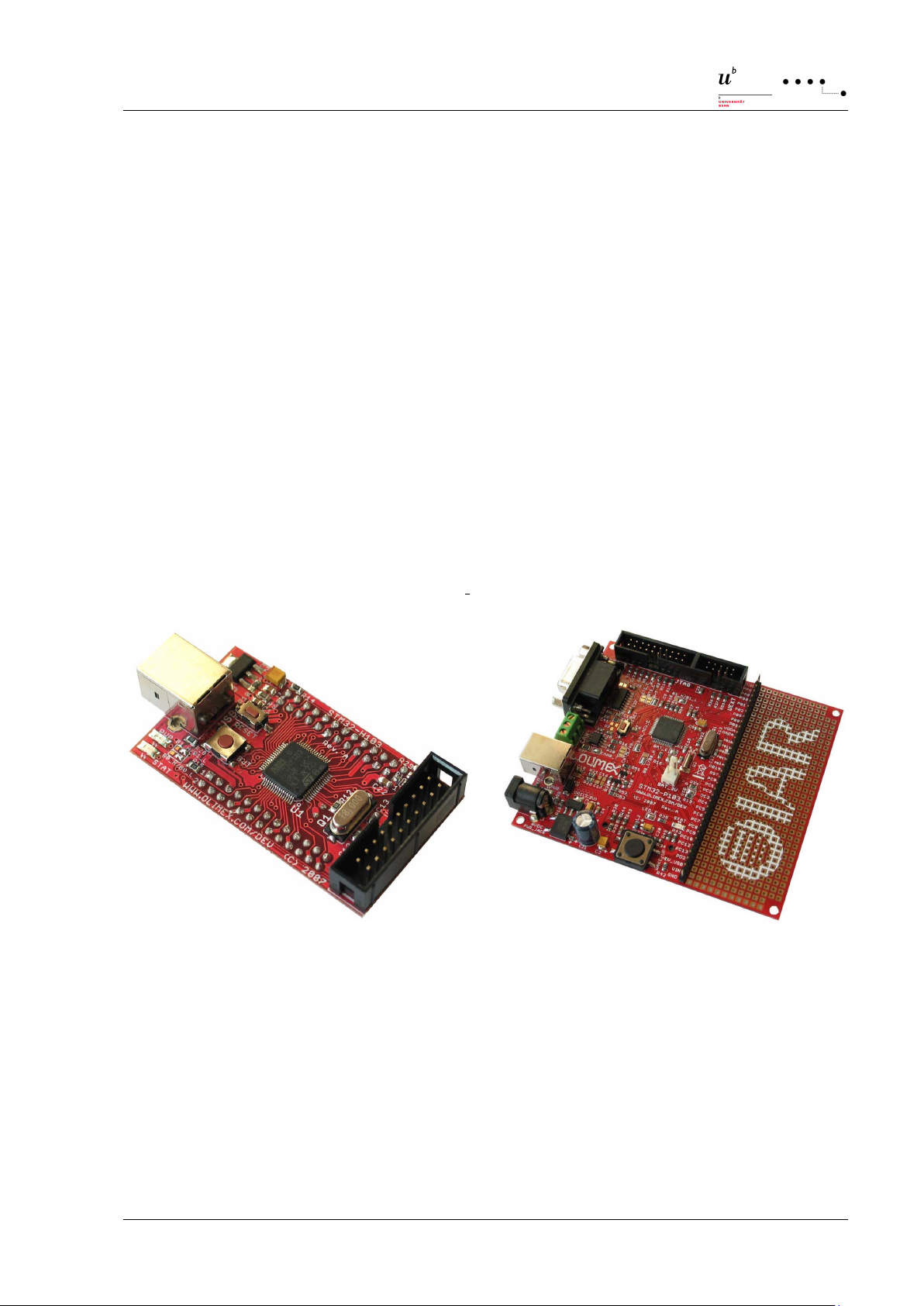
2.5 Development Boards
1 Intro
2.4.4 Interfaces
To be able to communicate with other devices we need interfaces:
• JTAG - Debug Interface:
The JTAG interface allows downloading the compiled code into the microcontroller and
debugging the code in real time. To be able to do this operation you have to use an JTAG
adapter to the USB or parallel port to the computer.
• USB - Universal Serial Bus:
Using a library one can communicate with an USB master. If you power the device over
USB, no wallplug or external power supply is needed.
• RS232, CAN, SPI I2C, I2S:
The serial interfaces can be used to communicate with any kind of devices or can be used
as debug/status interface.
2.5 Development Boards
We use the Olimex boards with our own BFH mother board extension. On both of these boards
the ARM Cortex M3 STM32F103RB produced by ST Microelectronics is present.
Both boards offer a LED on port PC12 (if LED E is bridged) and a button on PA0 (wake-up).
Figure 2.3: Development Board STM32H103 from
Olimex
Figure 2.4: Development Board STM32P103 from
Olimex
2.5.1 STM32H103 from Olimex
The STM32H103 is the minimal version of the Olimex STM32 board. It contains only a STM32F103RB
processor, USB connector with power adapter and LEDs. The STM32H103 can be connected via
the extension headers to the BFH mother board to connect to other interfaces. See Chapter 2.5.5
for more details.
Lukas Kohler 9
Page 18

1 Intro
2 System Description
2.5.2 STM32P103 from Olimex
The STM32P103 development board from Olimex is the extended version of the STM32H103. The
board includes:
• USB connector with power supply
• CAN driver and connector
• RS232 driver and connector
• JTAG with ARM 2x10 pin layout
• Reset button, user button, power and user LED
• SD/MMC card connector
• Voltage regulator 3.3V from USB or extension power jack connector (maximum power con-
sumption 0.25W at full speed)
• 8MHz and 32,768kHz oscillator (external clock and backup clock for RTC)
• UEXT connector that allows to connect to other modules
• Prototyping area
• Reset and wakeup circuit
• Dimensions: 100x90mm
2.5.3 Setup for Developing
In order to be able to develop software for the STM32F103RB , Keil µVision3 has to be installed
on a PC. If this is not yet the case install it according to Chapter 3. µVision3 is the tool used for
writing, compiling and testing software. The compiled source is then downloaded via a JTAG
adapter to the development board. Therefore the driver of the JTAG adapter has to be installed
too.
If the requirements above are fulfilled you can connect a USB cable from the PC to the development board STM32P103 or STM32H103. This connection is used for the power supply.
Connect the JTAG adapter to the development board STM32P103 or STM32H103 and connect a
USB cable from the JTAG adapter to the PC. This is used for downloading the software into the
processor and for debugging with the Keil toolchain (see Figure 2.5).
JTAG Adaptor
The JTAG Adaptor is needed for downloading the software into the processor and for debugging
with the Keil toolchain. According to Keil, different adapters can be used, such as:
• uLink from Keil
• jLink from Segger
• J-Link from IAR
I used the J-Link from IAR.
10 STM32 Cortex-M3 Tutorial
Page 19

2.5 Development Boards
1 Intro
Figure 2.5: Developing Software
2.5.4 Board Layout and Schematic
For schematics and board layouts please refer to the documents in
CD:/hardware/EvalBoards/Olimex/ .
2.5.5 BFH Mother Board
On the mother board the Olimex STM32H103 board is mounted on. The mother board has a
power supply and drivers for interfaces.
• The mother board uses the power supply form the STM32H103 board. Just connect the
STM32H103 with USB and the mother board is powered.
• 4 LEDs, lighting when tied to LOW (D1, connected with J24; D2-J25; D3-J28; D4-J28)
• 2 Buttons with a pull-up resistor, pressed gives a LOW state (S1, connected with J2; S2-J12)
• 1 Serial driver (RS232) (Rx-PA3; Tx-PA2; RTS-PA1; CTS-PA0 if DIPs are set according to
Figure 2.7)
• 2 potentiometer for analog inputs (R8-PC0; R9-PC1 when J26 and J27 are set)
Lukas Kohler 11
Page 20

1 Intro
2 System Description
• 1 CAN (Rx-PB8; Tx-PB9 if J1 and J3 are set; Resister on J6 (see Figure 2.8))
Figure 2.6: BFH Mother Board with STM32H103 from Olimex
Figure 2.7: RS232 directly connected (Pin 2: Rx, 3:
Tx, 5: GND)
Figure 2.8: CAN interface (Pin 2: CANL, 3/6:GND, 7:
CANH)
12 STM32 Cortex-M3 Tutorial
Page 21

3 Keil SDK
3.1 Introduction
The development of the firmware1we will write for the STM32 is done with the µVision3 from
Keil. This chapter shows how a simple project can be created, simulated and downloaded to the
target hardware.
3.2 Install µVision3
µVision3 can be found on the CD delivered with this documentation. Install µVision3 as well the
demo projects. This documentation refers to a standard installation done in the folder
C:/Keil/ARM/Boards/ST/STM32F10X EVAL/ .
A quick guide about µVision3 can be found at www.keil.com.
3.3 Install the Driver for the JTAG Adapter
Install the driver according the JTAG Adapter you are using.
3.4 Install the STM32 Peripheral Library
ST offers a free ARM-based 32-bit MCU STM32F10xxx standard peripheral library for programmers. This can be downloaded from www.st.com.
Direct Link: STM32F10x StdPeriph Lib
This library is used for accessing the peripherals like SPI or CAN. The STM32 Peripheral Library
from ST comes as well with different examples.
Unpack the library and copy the /Libraries/STM32F10x StdPeriph Driver/inc/ to
C:/Keil/ARM/INC/ST/STM32F10x and /Libraries/STM32F10x StdPeriph Driver/src to
C:/Keil/ARM/INC/RV31/LIB/ST/STM32F10x/ . This has to be done only once to update the
libraries.
Keil offers as well a peripheral configuration wizard but not for all peripherals. Chapter 4 introduces the peripherals and shows how they are configured - ether by the configuration wizard
from Keil or using the libraries from ST.
1
Software for microcontroller
13
Page 22

1 Intro
3 Keil SDK
3.5 Setting up a new Project
3.5.1 Preparation
Create a new directory for the project. Copy the files copy STM32 Init.c , STM32 Init.h ,
STM32 Reg.h and renameMe.c from /code/library into the new folder. Rename renameMe.c
to gpio.c . gpio.c This will be the main file.
• STM32 Init.c and STM32 Init.h : Configuration files for the STM32 processor
• STM32 Reg.h : Register file with defined addresses
3.5.2 Create a new project
Open µVision3 and create a new project by Project 7→ µVision3 Project... as shown in Figure 3.1 and
save it as gpio.uv2 .
Figure 3.1: Create a new project
The SDK needs to know your microcontroller and therefore you must specify the device to
STM32F103RB from STMicroelectronics (Figure 3.2).
Figure 3.2: Specify the device: STM32F103RB
The STM32 requires startup code which can be added automatically as shown in Figure 3.3. Click
on Yes.
14 STM32 Cortex-M3 Tutorial
Page 23

3.5 Setting up a new Project
1 Intro
Figure 3.3: Add the startup code to the project
The project has now been created. Now we need to add the files STM32 Init.c and gpio.c to
the project. Double click on Source Group 1 and add these two files.
3.5.3 Configure the Processor
Since we have added STM32 Init.c to the project we can use the Configuration Wizard to configure the processor. Double click STM32 Init.c and select Configuration Wizard (Figure 3.4). We
need the Clock Configuration and the General purpose I/O Configuration to be checked.
In the Clock Configuration do the following settings according to Figure 3.4
• Clock Control Register Configuration (RCC CR)
• Clock Configuration Register Configuration (RCC CFGR)
• HSE: External High Speed Clock [Hz]: 8000000 (8MHz) (given by the board)
Figure 3.4: Configuration wizard
General purpose I/O Configuration: We need to configure the GPIO to fast outputs:
• Check GPIOB: GPIO port B used and set all pins to General Purpose Output push-pull (max
speed 50MHz)
Embedded Flash Configuration: Set the settings acording to Figure 3.5.
Lukas Kohler 15
Page 24

1 Intro
3 Keil SDK
STM32F10x.s
assembler
STM32_Init.c
compiler
gpio.c
compiler
linker
STM32F10x.o
STM32F10x.lst
STM32_Init.o gpio.o
gpio.hex
gpio.map
Figure 3.5: Configuration wizard: Flash
3.5.4 Renaming the Target
Click on Project 7→ Manage 7→ Components, ... Rename Target 1 to Simulator by a double click on it
and press OK. We will use this setting for simulating the program on the PC.
3.6 Building
Open the main file gpio.c and insert the minimal code for a counter on GPIOB from Listing 3.1.
The building process starts by clicking on Project 7→ Rebuild all target files. This will assemble
STM32F10x.s and generate an object file (*.o) and its listing report (*.lst) according to Figure 3.6.
The c-files are compiled and object file (*.o) generated. The linker then puts together all the object
files and generates (with an ELF converter) the binary file and its report (*.map). The compiled
file can now be used for the simulation and not jet for downloading since we haven’t configured
the linker properly.
Figure 3.6: Building Process
The build creates an Executable File *.elf which is placed in the Output folder. When you use a
JTAG adapter, the ELF file is required to download to the board using JTAG. The build creates an
Intel HEX executable file which is placed in the same output folder for external program downloading through the serial port.
16 STM32 Cortex-M3 Tutorial
Page 25

3.7 Simulation
1 Intro
Listing 3.1: Minimal Code for a Counter on GPIOB
1 /∗ Name: gpio . c / P r o je c t gpi o 1
∗ De sc ri pt i on : Counter on GPIOB
∗ Vers io n : V1 .0 0 / 1 5. 07 .2 00 9 ∗/
# in c l ude <s t m3 2 f1 0 x l ib . h> // STM32F10x Lib ra r y D e fi ni ti on s
6 # inc l ude "STM32_Init.h" // STM32 I n it i a l i z a t i o n
i n t main ( void ) {
i n t i , j = 0 ; // c o unt er v a ri ab le s
s t m3 2 I n it ( ) ; // STM32 se t up
11
wh ile ( 1 ) { // Loop fo re ve r
j ++; // i nc re a s e f i r s t c oun te r
i f ( j ==1000 ) {
GPIOB−>ODR = ( GPIOB−>ODR & 0 xFFFF0000 ) | i ; // w ri te i t o GPIOB
16 j = 0;
i f ( i ==0xFFFF ) i = 0;
i ++;
}
}
21 }
3.7 Simulation
Before we download the project to the development board we’ll do a simulation in µVision3 to
see if everything works. Therefore click on Debug 7→ Start/Stop Debug Session or it’s icon. This will
open the debug mode and show a warning that you are using the evaluation mode. Click OK and
open the GPIOB port with Peripherals 7→ General Purpose I/O 7→ GPIOB.
Figure 3.7 shows the debug mode. In the top left corner the simulation is handled. To let the simulation run until a breakpoint is reached, press Run. In our example you’ll see the GPOIB counting
up binary and the variable i in the Watch Window increasing. You can change the variables in the
Watch Window by double clicking on them. A breakpoint can be set by a double click on the left
area of the code window. A running simulation can be interrupted by pressing the stop icon.
Pressing reset will set the CPU to its initial State.
In case you want to step through your code it’s not very nice to use breakpoints since these are
limited to 8. Therefore use the step commands. Step into will enter into every called function. Step
over doesn’t enter the function. Step out lets the code in the function execute, leave the function
and wait for further commands. Run to cursor line lets the code run until the line is reached where
the cursor is.
Lukas Kohler 17
Page 26

1 Intro
3 Keil SDK
Watch Window
GPIOB
Command
Window
actual Position
R
e
s
e
t
R
u
n
S
t
o
p
I
n
t
o
O
v
e
r
O
u
t
S
t
a
r
t
/
S
t
o
p
D
e
b
u
g
S
e
s
s
i
o
n
Simulation Step
R
u
n
t
o
C
u
r
s
o
r
l
i
n
e
3.7.1 Window update
ate selectThe peripherals are updated when an event from the user occours, e.g. clicking on an
input check box. For a periodical update select View 7→ Periodic Window Update.
3.7.2 Serial Window
To simulate a serial interface open View 7→ Serial Window 7→ UART x.
3.7.3 Performance Analyzer
To analyse the efficiency of your code open View 7→ Performance Analyzer. This window shows the
time and amount a function is called.
Figure 3.7: Debug Mode
18 STM32 Cortex-M3 Tutorial
Page 27

3.8 Configuring the Target
1 Intro
3.8 Configuring the Target
After the simulation on the computer we know that our program works and in case of errors
we have corrected them. Now there is need of configuring the linker and the debug utilities.
Therefore quit the debug mode first. Klick first on the icon 1 according to Figure 3.11. You already
know the appearing window. Now click on New Project Target, name it STM32H103 and click OK.
Select now the created target on the left side of the icon 1. Klick now on the icon 2 according to
Figure 3.11. !
The processor won’t run if is not configured as shown in the Figures 3.11 - 3.15!
Go to the tab Debug and select Use: Your JTAG Adapter. In the tab Utilities select Use Target Driver
for Flash Programming: Your JTAG Adapter. Click on Settings and there on Add. Select STM32F10x
Med-density Flash2and click Add and twice OK.
Figure 3.8: Options for Output Figure 3.9: Options for Listing
Figure 3.10: Options for Linker
2
In µVision before version 3.7 select STM32F10x 128kB Flash
Lukas Kohler 19
Page 28

1 Intro
Figure 3.11: Options for Target
3 Keil SDK
Figure 3.13: Options for Debug Settings
Figure 3.12: Options for Debug
Figure 3.15: Options for Utilities Settings
Figure 3.14: Options for Utilities
Connect now the BFH motherboard with the mounted STM32-H103 to the computer according to
Chapter 2.5.5.
20 STM32 Cortex-M3 Tutorial
Page 29

3.9 Downloading
1 Intro
3.9 Downloading
The command Flash 7→ Download or its icon download the compiled file to the STM32 and let it
run if the option Reset and Run is set (see Figure 3.15). If the program doesn’t start push the reset
button on the STM32-H103 board. A program downloaded into the flash will stay in the flash
even if the power supply is removed.
Our program will count up on GPIOB. Connect therefore the J24 with PB8, J25 with PB9, J28-PB10,
J29-PB11. If you connect a LED to PB0 you won’t see anything since the switching frequency is to
high. That’s why we use PB8..PB11. You should see the binary counter on D1 - D4.
3.10 Debugging
In the debugging mode you have the same options as in the Simulation mode. Refer therefore to
Chapter 3.7.
3.11 Serial Terminal
hTerm ( CD:/tools/hterm/HTerm.exe ) is a powerfull tool for analysing serial communication.
No installation is needed. Select the Port you want to communicate and the desired baud rate,
press connect and hTerm will display you the received data.
Figure 3.16: hTerm
Lukas Kohler 21
Page 30

1 Intro
3 Keil SDK
3.12 Documenting Source Code
Documenting the source code is very important that other users of the code are able to understand
it. In this documentation Doxygen has been used. Listing 3.2 shows the used commands for
Doxygen. After running Doxygen a html help is generated. It is stored at
CD:/code/doc/html/index.html.
Listing 3.2: Source Code Documentation with Doxygen
/∗∗
∗ @ f i le u sa r t1 . c
∗ @b ri e f USART usage f or STM32: put Char ( ) .
4 ∗
∗ <H3>P ro je c t : us art 1</H3>
∗
∗ Sends p er i o di c al ly th e c ha r a ct er ’ ∗ ’ with 9600Baud t o i t s h ost .
∗ S e t ti n g s ( s ee C onf ig u ra t io n Wizard o f STM 32 Ini t ) :
9 ∗ − 9600 Baud
∗ − 8/1/N
∗
∗ @author Lukas Kohl e r / BFH−TI
∗ @date 15 . 0 7. 20 09
14 ∗/
22 STM32 Cortex-M3 Tutorial
Page 31

4 Peripherals
4.1 Getting Started
The STM32F103RB is a very complex processor. There is not just one datasheet for all information.
• Datasheet: CD:/datasheet/ST/STM32F103x8B.pdf
Gives a general introduction to the STM32F103RB processor. Pinouts, electrical, thermal and
package characteristics are described there. Refer to the datasheet if you want to calculate
the power consumption or to see the pin relation between GPIO and pins (e.g. to which pin
is GPIOA1 connected to).
• Reference manual RM008: CD:/datasheet/ST/RM0008 Reference Manual.pdf
Describes the function inside the processor, such as periphery, clock management or power
control. Refer to this manual for programming.
• CD:/code/self/ offers proved examples for µVision3.
• The Firmware Library stm32f10x stdperiph lib (see also Chapter 4.3) offers examples
CD:/code/stm32f10x stdperiph lib/Project/STM32F10x StdPeriph Examples/
• Insider’s Guide from Hitex CD:/datasheet/hitex-guide STM32
Gives a general introduction to the STM32F103RB processor.
• More help can be found on http://www.st.com/mcu/devicedocs-STM32F103RB-110.html
and http://www.stm32circle.com
4.2 Configuration Wizard
gpio2 F GPIO usage by register acces and Configuration Wizard.
Keil offers a Configuration Wizard (see Figure 4.1) which lets the user configure the processor
registers without need of knowing the specific registers. This wizard can be used only for simple
programs like controlling GPIO or serial interface. In case you need to use more complex functions
like SPI, I2C or even DMA we suggest you to use the firmware library from STMicroelectronics
(see Chapter 4.3). In this document the Configuration Wizard is used whenever possible.
The access of the register can’t be done by the Configuration Wizard, the Firmware Library (see
Chapter 4.3) or direct register access (see Chapter 4.4) has to be used.
b
23
Page 32

1 Intro
b
4 Peripherals
4.3 Firmware Library (FWLib)
gpioFwLib F GPIO usage by register access.
STMicroelectronics offers a firmware library which allows you to access to peripherals and registers easily and with a clean interface. The installation is shown in Chapter 3.4. The principle of
using the FWLib is easy and straight forward since the policy is equal for all peripherals. This
principle is shown here with the GPIO.
1. Include the FWLib to the project by adding ether the precompiled library or the uncompiled
c files like stm32f10x PERIPHERAL.c . The c library files are located at
C:/Keil/ARM/RV31/LIB/ST/STM32F10x and should be added by the Keil project in the
folder lib.
2. Add #include <stm32f10x_PERIPHERAL.h> at the begin of your main file (where PE-
RIPHERAL stands for the peripheral you want to use, e.g. SPI or GPIO). The header files are
located at C:/Keil/ARM/INC/ST/STM32F10x and automaticly included by
µVision.
3. Use the functions from the FWLib (like GPIO Init()). The functions are described in the file
stm32f10x stdperiph lib um.chm that comes with the FWLib.
The FWLib offers structures for the peripherals. This structure is created and initialized with:
Listing 4.1: Structure creation and initialization
15 G PIO I n itT y pe D e f GP IO I ni tS tr uc t ur e ;
GP IO S tr uc tI ni t(& GPI O In it St ru ct ur e ) ;
The properties then are set with:
Listing 4.2: Setting the Properties
GP IO I ni tS tr uc tu r e . GPIO Pin = GPIO Pin 5 | G P IO Pin 7 ;
GP IO I ni tS tr uc tu r e . GPIO Speed = GPIO Speed 50MHz ;
GP IO I ni tS tr uc tu r e . GPIO Mode = GPIO Mode AF PP ;
20 GP I O I n it (GPIOA, &G PI O In it St ru ct ur e ) ;
The FWLib is used in this document for the examples ADC, CAN, I2C and SPI.
24 STM32 Cortex-M3 Tutorial
Page 33

4.4 Register Access
1 Intro
4.4 Register Access
gpioRegister F GPIO usage by register access. Instead of using the FwLib the registers can be
accessed directly.
The properties then are set with:
Listing 4.3: Setting the GPIO Register by direct access
/∗∗
∗ Se t up t he GPIO r eg is t e r s (GPIOA as i n put and GPIOB as out p ut )
∗/
voi d i ni tG pi o Re gi st e r ( void ) {
25 // GPIOA: In pu t w i t h p u ll up /pulldown
GPIOA−>CRH = 0 x888 8 88 88 ;
GPIOA−>CRL = 0 x8888 88 8 8 ;
// GPIOB : Output push−p ull , 50MHz
GPIOB−>CRH = 0 x3 33 33 3 33 ;
30 GPIOB−>CRL = 0 x33 3 33 33 3 ;
}
b
Lukas Kohler 25
Page 34

1 Intro
4 Peripherals
4.5 General Purpose Input/Output (GPIO)
GPIOs are used for reading an input or setting an output. The GPIOs of the STM32F103RB can all
be used as digital or analog inputs.b
b
b
gpio1 F Shows a counter on GPIOB.
gpio2 F Reads the inputs of GPIOA and puts them on GPIOB.
gpio3 F Pressing buttons S1, S2 move the lit LED. S1 moves the lit LED to the right, S2 to the left.
4.5.1 Configuration
The configuration is done with the Settings Wizard (see Chapter 3.5.2 for more information), shown
in Figure 4.1.
GPIOA to GPIOD can be set to different modes:
• Input
– Analog: Used to route the signal to an AD converter (see Chapter4.13)
– Floating: Used as a ”normal” input
– Input with pull-up / pull-down resister
• Output
– Push-pull (max speed 2MHz, 10MHz or 50MHz): Used as a ”normal” output
– Open-drain (max speed 2MHz, 10MHz or 50MHz): Used in a system with different
nodes having access to the same wire.
• Alternate Function (AF): Used for Oscillator, CAN, JTAG, ADC, Timer, USART, I2C and SPI
– Alternate Function push-pull (max speed 2MHz, 10MHz or 50MHz)
– Alternate Function open-drain (max speed 2MHz, 10MHz or 50MHz)
Figure 4.1: GPIO Configuration Wizard
26 STM32 Cortex-M3 Tutorial
Page 35

4.5 General Purpose Input/Output (GPIO)
1 Intro
Figure 9. Basic structure of a standard I/O port bit
Alternate Function Output
Alternate Function Input
Push-pull,
open-drain or
disabled
Input data register
Output data register
Read/write
From on-chip
peripheral
To on-chip
peripheral
Output
control
Analog Input
on/off
on/off
I/O pin
V
DD
V
DD
V
SS
V
SS
TTL Schmitt
trigger
V
SS
V
DD
Protection
diode
Protection
diode
on/off
Input driver
Output driver
P-MOS
N-MOS
Read
Bit set/reset registers
Write
ai14781
4.5.2 Driver
4.5.3 Set Output
GPIOB−>ODR = (GPIOB−>ODR & 0 xFFFF0000 ) | yourValu e ; // p ut s yourValue on
GPIOB
4.5.4 Read Input
in p ut = (GPIOA−>IDR & 0 x0000FFF F ) ; // r e ad in put s on GPIOA
Lukas Kohler 27
Figure 4.2: GPIO driver
Listing 4.4: Set Output
Listing 4.5: Read Input
Page 36

1 Intro
4 Peripherals
4.6 Serial Interface (USART)
The serial interface is used to communicate with other devices. Nowadays it is often used as
debug interface to send information to a host like a PC. UARTs are commonly used in conjunction
with other communication standards such as EIA RS-232.b
b
b
b
b
usart1 F sends periodically the character ”*” with 9600Baud to its host.
usart2 F sends periodically the ASCII characters with 9600Baud to its host.
usart3 F polls the incoming data and sends them back to its sender (9600Baud)
usart4 F sends periodically the string ”Hello World” with 115200Baud to its host using printf().
usartIrq1 F the data and sends them back to its sender (9600Baud, uses IRQ)
4.6.1 Ways of Operation: Polling versus Interrupts
The serial interface can be read and written in two different ways:
• Polling: The input register is read periodically for new data.
• Interrupts: The input register generates an interrupt in case that there is new data available.
The ISR (see Chapter 4.10) then is called and in there the data are sent. This method is more
efficient but more complex.
4.6.2 Using Polling
Configuration
The configuration is done with the Settings Wizard (see Chapter 3.5.2 for more information), shown
in Figure 4.3.
Figure 4.3: USART Configuration Wizard
Send Data
Copy the files serial.c and serial.h and use the function int ser putchar (int c).
Listing 4.6: Send Data
wh ile ( ! ( USARTx−>SR & USART FLAG TXE) ) ; // wa i t u nt i l ready
35 USARTx−>DR = ( yo ur Cha r acte r & 0 x1FF ) ; // sen d s you rC har a cte r
28 STM32 Cortex-M3 Tutorial
Page 37

4.6 Serial Interface (USART)
1 Intro
Read Data
Copy the files serial.c and serial.h and use the function int ser getchar (void).
Listing 4.7: Receive Data
wh ile ( ! ( USARTx−>SR & USART FLAG RXNE) ) ; // wai t u nt il a ch ar ha s been
re ce iv e d
you rCha ra cte r = ( USARTx−>DR & 0x1FF ) ; // re a d c ha ra ct er from the b uf fe r
4.6.3 Using Interrupts
Configuration
The configuration is done with the Settings Wizard shown in Figure 4.4. The function
void USART2 IRQHandler (void) is called when an interrupt, configured in the Settings Wizard,
occurs. Refer to the example usartIrq1 for more information.
Figure 4.4: USART Configuration Wizard (using Interrupts)
4.6.4 Driver
The data are transmitted on the system voltage level1to the converter and there converted to the
RS232 level2. The RS232 interface can then be connected to any PC. For a minimum communication three wires are required:
• TxD: Tranceive Data
• RxD: Receive Data
• GND: Common Ground
Figure 4.5 shows the driver included in the STM32F103RB .
1
System voltage: +3.3V (=HIGH) and 0V (= LOW)
2
RS232 level: +12V (=LOW = 0) and -12V (= HIGH = 1)
Lukas Kohler 29
Page 38

1 Intro
4 Peripherals
Universal synchronous asynchronous receiver transmitter (USART) RM0008
Figure 236. USART block diagram
WAKE
UP
UNIT
RECEIVER
CONTROL
SR
TRANSMIT
CONTROL
TXETC RXNEIDLEORE NE FE
USART
CONTROL
INTERRUPT
CR1
M WAKE
Receive Data Register (RDR)
Receive Shift Register
Read
Transmit Data Register (TDR)
Transmit Shift Register
Write
SW_RX
TX
(DATA REGISTER) DR
TRANSMITTER
CLOCK
RECEIVER
CLOCK
RECEIVER RATE
TRANSMITTER RATE
f
PCLKx(x=1,2)
CONTROL
CONTROL
/16
CONVENTIONAL BAUD RATE GENERATOR
SBKRWURETE
IDLERXNE
TCIETXEIE
CR1
UE PCE PS
PEIE
PE
PWDATA
IRLP
SCEN
IREN
DMAR
DMAT
USART Address
CR2
CR3
IrDA
SIR
ENDEC
BLOCK
LINE
CKEN CPOL
CPHA LBCL
SCLK CONTROL
SCLK
CR2
GT
STOP[1:0]
NACK
DIV_Mantissa
15
0
RE
USART_BRR
/USARTDIV
TE
HD
(CPU or DMA)
(CPU or DMA)
PRDATA
Hardware
flow
controller
CTS LBD
RX
IRDA_OUT
IRDA_IN
nRTS
nCTS
GTPR
PSC
IE
IE
DIV_Fraction
4
USARTDIV = DIV_Mantissa + (DIV_Fraction / 16)
Figure 4.5: USART driver
Figure 4.6: USART Names of the additional communication wires
30 STM32 Cortex-M3 Tutorial
Page 39

4.6 Serial Interface (USART)
1 Intro
The baud rate generator generates the internal clock for sending and receiving data. The serial
protocol is shown in Figure 4.7 (1 start bit, 8 data bits, 1 stop bit and 1 parity).
Figure 4.7: USART Serial Protocol
4.6.5 Pinning
USART1
Default
Wire GPIO Pin
CK PA8 41
TX PA9 42
RX PA10 43
CTS PA11 44
RTS PA12 45
USART2
Default
Wire GPIO Pin
CTS PA0 14
RTS PA1 15
TX PA2 16
RX PA3 17
CK PA4 18
USART3
Remapped
Wire GPIO Pin
CK - TX PB6 58
RX PB7 59
CTS - RTS - -
Remapped 7→ only on LQFP100!
Wire GPIO Pin
CTS PD3 RTS PD4 TX PD5 RX PD6 CK PD7 -
Default
Wire GPIO Pin
TX PB10 29
RX PB11 30
CK PB12 33
CTS PB13 34
RTS PB14 35
Lukas Kohler 31
Remapped
Wire GPIO Pin
TX PC10 51
RX PC11 52
CK PC12 53
CTS - RTS - -
Page 40

1 Intro
b
4 Peripherals
4.7 System Timer (SysTick)
sysTick F sets up a system timer routine and shows a running light on GPIOB. The system
timer is a periodical timer that can be set up easily with the configuration wizard
(see Figure 4.8).
The Cortex core includes a 24-bit down counter, with auto reload and end of count interrupt. This
is intended to provide a standard timer for all Cortex-based microcontrollers. The SysTick timer
is intended to be used to provide a system tick for an RTOS, or to generate a periodic interrupt for
scheduled tasks. The SysTick Control and status register in the Cortex-M3 System control space
unit allows you to select the SysTick clock source. By setting the CLKSOURCE bit the SysTick
timer will run at the CPU frequency. When cleared the timer will run at 1/8 CPU frequency.
4.7.1 Configuration
Enable the System Timer Configuration in the configuration wizard and select a clock source. Choose
the time interval and enable the interrupt. The function void SysTick Handler (void) above
the main()-routine gets called when the sysTick interrupt occurs.
Figure 4.8: System Timer Configuration Wizard
32 STM32 Cortex-M3 Tutorial
Page 41

4.8 Timer (TIM)
1 Intro
4.8 Timer (TIM)
timer F Running light on GPIOB
The STM32 offers different kind of individually configurable timers:
• General-purpose timer (TIMx): They may be used for a variety of purposes, including mea-
suring the pulse lengths of input signals (input capture) or generating output waveforms
(output compare and PWM).
• Basic timer (TIM6 and TIM7): They may be used as generic timers for time-base generation
but they are also specifically used to drive the digital-to-analog converter (DAC). In fact,
the timers are internally connected to the DAC and are able to drive it through their trigger
outputs.
• Advanced-control timers (TIM1 and TIM8): It may be used for a variety of purposes, in-
cluding measuring the pulse lengths of input signals (input capture) or generating output
waveforms (output compare, PWM, complementary PWM with dead-time insertion).
The timers consist of a 16-bit auto-reload counter driven by a programmable prescaler. The timers
are completely independent, and do not share any resources. They can be synchronized together
(not TIM6 and TIM7).
b
In the µVision configuration wizard the timers TIM1 ... TIM4 can be configured directly. The other
timers have to be configured using the FwLib.
4.8.1 Configuration
In the configuration wizard (see Figure 4.9) the timer interrupt has to be enabled and configured.
Figure 4.9: Timer Configuration Wizard
The function void TIM1 UP IRQHandler (void) gets called after the TIM1 period has expired.
Lukas Kohler 33
Page 42

1 Intro
b
4 Peripherals
4.9 Pulse Width Modulation (PWM)
pwm1 F Lets PB8 blink with 1Hz 50% duty-cycle and PB9 with 25% using the PWM function of
the timer TIM4.b
pwm2 F LEDs PB8, PB9 are dimmed using the PWM function of TIM4 channel3 and channel4
4.9.1 Configuration
The timer TIM4 is used for the PWM signal. The channel 3 is mapped by default to PB8 and
channel 4 to PB9.
Figure 4.10: PWM Configuration Wizard
34 STM32 Cortex-M3 Tutorial
Page 43

4.10 External Interrupts (IRQ)
1 Intro
4.10 External Interrupts (IRQ)
b
extInt F Pin PA0 is configured to generate an external interrupt. Pressing this button will toggle
a LED.
One of the key improvements of the Cortex core over the earlier ARM CPUs is its interrupt structure and exception handling. The ARM7 and ARM9 cores had two interrupt lines: The fast interrupt and the general purpose interrupt line. These two interrupt lines had to support all of
the interrupt sources within a given manufacturer’s microcontroller. How this was done varied
according to the implementation, so while the techniques used were broadly the same, the implementation differed between manufacturers.
Since the interrupt scheme is implemented in the Cortex-M3 core, the way of operating is for all
microcontroller s using this core equal.
4.10.1 Configuration
In the configuration wizard (see Figure 4.11) the external interrupts have to be enabled and con-
figured to a input pin. !
Note that this input in the GPIO section as well has to be configured as an input!
Figure 4.11: External Interrupt Configuration Wizard
4.10.2 Functionality
An event (rising or/and falling edge, according to the configuration) on EXTI0 will call the function void EXTI0 IRQHandler(void). In this function, the interrupt service routine (ISR) first
check which ISR is pending by reading the pending register EXTI PR. At the end of the ISR you
have to clear the pending ISR in the EXTI PR. See Listing 4.8 for an ISR example.
Listing 4.8: ISR
voi d EXTI0 IRQHandle r ( void ) {
i f ( EXTI−>PR & (1< < 0) ) { // EXTI0 i nt er ru p t pending ?
40 // your ISR co de h e re
EXTI−>PR | = (1< < 0) ; // cl ea r pending i nt e r ru pt
}
}
Lukas Kohler 35
Page 44

1 Intro
b
4 Peripherals
Note that the inputs form PA0, PB0, .. PG0 are mapped together to EXTI0. The same is the issue
for all the inputs with the same number.
4.11 Watchdog
iwdg F Shows how the watchdog is configurated.
4.11.1 Configuration
Select the timeout time in the configuration wizard. During this time your program has to clear
the watchdog by loading a specific value into IWDG7→KR. If this desn’t happen the watchdog will
reset the CPU.
Figure 4.12: Watchdog Configuration Wizard
b
b
b
4.12 Real Time Clock (RTC)
rtc1 F RTC is configured to generate a second and an alarm interrupt which turns a LED on.
rtc2 F 24h clock, time is sent over the serial interface to its host (115200Baud).
rtc3 F rtc2 including resetting of the RTC when a button is pressed.
The RTC provides a stable clock for the processor. It is able to generate a second interrupt which
gets called every second. An alarm can be set to a specific time. Is this time up an interrupt is generated. An overflow interrupt occurs when the 32-bit RTC counter overflows. Unfortunately the
RTC doesn’t offer registers for time and date, only for the time in seconds in the two 16-bit register
RTC CNTH (higher 16-bits) and RTC CNTL (lower 16-bits). The alarm registers (RTC ALRH and
RTC ALRL) is similar to the time register.
Figure 4.13: RTC Configuration Wizard
36 STM32 Cortex-M3 Tutorial
Page 45

4.13 Analog to Digital Converter (ADC)
1 Intro
Hour Minute Second RTC CNTH RTC CNTL Seconds
00 00 01 0x0000 0x0001 1s
00 01 01 0x0000 0x003D 3601s
23 00 01 0x0001 0x4371 82801
Table 4.1: Configuration of the register RTC CNTL and RTC CNTH
Listing 4.9: RTC ISR
voi d RTC IRQHandler ( void )
45 {
i f (RTC−>CRL & (1 <<0) ) { // c h eck second f la g
RTC−>CRL &= ˜ (1 < < 0) ; // c le a r second f la g
// your code
}
50
i f (RTC−>CRL & (1 <<1) ) { // c h eck alarm f la g
RTC−>CRL &= ˜ (1 < < 1) ; // c le a r alarm f la g
// your code
}
55
i f (RTC−>CRL & (1 <<2) ) { // c h eck Overf low f la g
RTC−>CRL &= ˜ (1 < < 2) ; // c le a r Overflow f la g
// your code
}
60 } // end RTC IRQHandler
4.13 Analog to Digital Converter (ADC)
ad1 F reads the values and writes them on the serial interface (115200Baud)
4.13.1 Conversion Modes
The AD converters of the STM32F103RB can operate in two different modes:
• Singleshot: The program triggers to read the value once.
• Scan Mode: In scan mode, automatic conversion is performed on a selected group of analog
inputs.
STM32F103RB have two 12-bit Analog to Digital Converters which share up to 16 external channels. Additional logic functions embedded in the ADC interface allow:
• Simultaneous sample and hold
• Interleaved sample and hold
• Single shot
The ADC can be served by the DMA controller. An analog watchdog feature allows very precise monitoring of the converted voltage of one, some or all selected channels. An interrupt is
generated when the converted voltage is outside the programmed thresholds.
b
Lukas Kohler 37
Page 46

1 Intro
4 Peripherals
The events generated by the standard timers (TIMx) and the Advanced Control timer (TIM1) can
be internally connected to the ADC start trigger, injection trigger, and DMA trigger respectively,
to allow the application to synchronize A/D conversion and timers.
Listing 4.10: ADC Init
/∗ I n i t i a l i z e s th e Analog/ Di g i ta l c o nv er te r
PC1 (ADC Channel10 ) i s used as a na lo g inp u t ∗/
voi d a dc I ni t ( void ) {
65 RCC−>APB2ENR |= RCC APB2ENR ADC1EN; // en abl e p er ip he ra l c lo ck
f o r ADC1
ADC1−>SQR1 = 0 x0 0 00 00 00 ; // only one co nve rs ion
ADC1−>SMPR2 = 0 x 00 00 00 2 8 ; // s et sample ti me c ha nn el1
( 5 5 ,5 c y c le s )
ADC1−>SQR3 = 1 0; // s et ch a nnel 1 0 as 1 st
co n ver sio n
70
ADC1−>CR1 = 0 x00 00 0 10 0 ; // u s e i n dep e nde n t mode,
SCAN mode
ADC1−>CR2 = 0 x000E0003 ; // data a li gn r ig ht , c ont
co n ver sio n
// EXTSEL = SWSTART
// e n abl e ADC, no e xt er na l
Tr ig g er
75 ADC1−>CR2 |= 0 x0 0 50 00 00 ; // s t a r t SW c o nve rsi on
}
Listing 4.11: Read ADC Values
/∗ re ad a con v erte d valu e from th e Analog/ Di g it al c on v er te r ∗/
unsigned ch a r adc G e t ( void ) {
unsigned s ho r t v al ;
80
wh ile ( ! ( ADC1−>SR & ADC SR EOC) ) ; // wai t t i l l end o f
co n ver sio n
va l = ADC1−>DR & ADC DR DATA; // Get co nve rs io n r es ul t
va l = ( val >> 4 ) & 0 xFF ; // S ca le an a lo g va lue t o 8
b i ts
85 r et u rn ( v a l ) ;
}
38 STM32 Cortex-M3 Tutorial
Page 47

4.13 Analog to Digital Converter (ADC)
1 Intro
Figure 20 shows a single ADC block diagrams and Tab l e 4 3 gives the ADC pin description.
Figure 20. Single ADC block diagram
ADCx_IN0
ADCx_IN1
Analog to digital
converter
ADCx_IN15
Analog
MUX
ADCCLK
ADC Interrupt to NVIC
GPIO
Ports
Analog watchdog
Address/data bus
Low Threshold (12 bits)
Compare Result
High Threshold (12 bits)
Flags
enable bits
EOC
AWD
Analog watchdog event
V
DDA
V
SSA
V
REF+
V
REF-
Interrupt
TIM1_CH2
TIM1_CH3
TIM2_CH2
TIM3_CH4
From ADC prescaler
(16 bits)
End of conversion
channels
Injected
channels
End of injected conversion
JEOC
EOCIE
AWDIE
JEOCIE
up to 4
up to 16
Regular data register
(4 x 16 bits)
Injected data registers
Regular
Start trigger
(regular group)
EXTSEL[2:0] bits
EXTRIG
TIM1_CH1
TIM4_TRGO
EXTI_15
TIM1_CH4
TIM2_TRGO
TIM2_CH1
TIM3_TRGO
Start trigger
(injected group)
JEXTSEL[2:0] bits
TIM1_TRGO
TIM4_CH4
JEXTRIG
bit
bit
DMA request
Temp. sensor
V
REFINT
TIM2_CH3
TIM1_CH3
TIM8_CH1
TIM8_CH4
TIM3_CH1
TIM5_TRGO
TIM1_CH4
TIM4_CH3
TIM8_CH2
TIM8_TRGO
JEXTSEL[2:0] bits
TIM1_TRGO
TIM5_CH1
Triggers for ADC3
(1)
Start trigger
(injected group)
JEXTRIG
bit
Start trigger
(regular group)
EXTRIG
bit
EXTSEL[2:0] bits
TIM5_CH4
TIM5_CH3
EXTI_11
TIM8_TRGO
(2)
ADCx_ETRGREG_REMAP bit
TIM8_CH4
(2)
ADCx-ETRGINJ_REMAP bit
ai14802d
Figure 4.14: Single ADC Block Diagram
Lukas Kohler 39
Page 48

1 Intro
4 Peripherals
SRAM memory for data transmission and reception, and so they cannot be used
concurrently (the shared SRAM is accessed through CAN and USB exclusively). The USB
and CAN can be used in the same application but not at the same time.
In today’s CAN applications, the number of nodes in a network is increasing and often
several networks are linked together via gateways. Typically the number of messages in the
system (and thus to be handled by each node) has significantly increased. In addition to the
application messages, Network Management and Diagnostic messages have been
introduced.
● An enhanced filtering mechanism is required to handle each type of message.
Furthermore, application tasks require more CPU time, therefore real-time constraints
caused by message reception have to be reduced.
● A receive FIFO scheme allows the CPU to be dedicated to application tasks for a long
time period without losing messages.
The standard HLP (Higher Layer Protocol) based on standard CAN drivers requires an
efficient interface to the CAN controller.
Figure 190. CAN network topology
CAN node 1
CAN node 2
CAN node n
CANCAN
High
Low
CANCAN
Rx Tx
CAN
Transceiver
CAN
Controller
MCU
CAN Bus
Application
4.14 Controller Area Network (CAN)
Controller-area network (CAN or CAN-bus) is a vehicle bus standard designed to allow microcontrollers and devices to communicate with each other within a vehicle without a host computer.
It was designed specifically for automotive applications but is now also used in other areas. Development of the CAN-bus started originally in 1983 at Robert Bosch GmbH. The protocol was
officially released in 1986 at the Society of Automotive Engineers (SAE) congress in Detroit, Michigan. The first CAN controller chips, produced by Intel and Philips, came on the market in 1987.
Bosch published the CAN 2.0 specification in 1991.
The STM32F103RB CAN is compliant with specifications 2.0A and B (active) with a bit rate up to
1 Mbit/s. It can receive and transmit standard frames with 11-bit identifiers as well as extended
frames with 29-bit identifiers. It has three transmit mailboxes, two receive FIFOs with 3 stages
and 14 scalable filter banks.
can1 F Sends the string hello with 500Bit/s over the CAN. Receives the internal looped signalb
using polling (mode: CAN Mode LoopBack). Therefore no message can be received! Uses the
serial interface at 115200Baud.
can2 F As can1 but able to receive CAN data (mode: CAN Mode Normal).b
Figure 4.15: CAN Network Topology
!
By default the CAN and USB share same pins PA11/EXT1-1 and PA12/EXT1-3, so you can’t use
!
both CAN and USB on same time. A remap (see example) can be done to PB8/PB9.
Make sure you set up a filter even if you want to receive all CAN messages.
40 STM32 Cortex-M3 Tutorial
Page 49

4.15 Inter IC Bus (I2C)
1 Intro
4.14.1 CAN Analyzer
To understand the data transmitted on the CAN
you need a CAN Analyzer. I used the PCANUSB from www.peak-system.com. This CAN in-
terface allows you to see the messages transmitted on the CAN bus.
4.14.2 Pinning
Figure 4.16: CAN Analyzer Software
Default
Wire GPIO Pin
CANRX PA11 44
CANTX PA12 45
Remapped
Wire GPIO Pin
CANRX PB8/PD0 61/5
CANTX PB9/PD1 62/6
4.15 Inter IC Bus (I2C)
i2c1 F Writes data to the I
STM32F103RB have two I2C bus interfaces which can operate in multimaster and slave modes.
They can support standard and fast modes. They support dual slave addressing (7-bit only) and
both 7/10-bit addressing in master mode. A hardware CRC generation/verification is embedded.
They can be served by DMA and they support SM Bus 2.0/PM Bus.
Introduction
The I2C interface3is a serial interface with three wires.
2
C bus b
The clock on the one directional wire SLC is generated by the master with a fix frequency. This
line is stable (normally high) when no data are transmitted on th data line. The second wire SDA
is bi directional and used for the data communication between the master and the slave4.
The wiring is according to Figure 4.17.
3
IIC, I2C (Inter IC Bus) were developed and registered by Phillips and saved as a trademark. Atmel uses the name
TWI.
4
The slave is controlled by the master.
Lukas Kohler 41
Page 50

1 Intro
4 Peripherals
Figure 4.17: I2C Wiring
The third line is used when a slave want to tell the master something. An interrupt is generated
then.
4.15.1 Physical layer
I2C Definitions
• Data can only be transmitted when the bus is not active.
• As long as the clock is high, the data line is not allowed to change.
• When no data are transmitted, SCL and SDA are high.
Figure 4.18: I2C Communication Protocol
4.15.2 Communication Protocol
5
1. The data transfer starts with the start bit. The clock is High, data changes from High to Low,
see Figure 4.20
2. The slave address is transmitted.
3. The R/W Bit (see Figure 4.21 and 4.22) defines if data are read from the slave (R/W = 0) or
if data are written to the slave (R/W = 1).
5
A change of the data during a high clock is interpreted as a control command.
42 STM32 Cortex-M3 Tutorial
Page 51

4.15 Inter IC Bus (I2C)
1 Intro
AI00587
DATA
CLOCK
DATA LINE
STABLE
DATA VALID
START
CONDITION
CHANGE OF
DATA ALLOWED
STOP
CONDITION
DATA OUTPUT
BY RECEIVER
DATA OUTPUT
BY TRANSMITTER
SCL FROM
MASTER
START
CLOCK PULSE FOR
ACKNOWLEDGEMENT
12 89
MSB LSB
DATA
CLOCK
DATA LINE
STABLE
DATA VALID
START
CONDITION
CHANGE OF
DATA ALLOWED
STOP
CONDITION
M41T81
=0) is
and the internal address pointer is incremented to
the next address locati on on the reception of an
acknowledge clock. The M41T81 slave receiver
will send an acknowledge clock to the master
transmitter after it has received t he sla ve address
see Figure 13, page 12 and aga in after it has re-
ceived the word address and each data byte.
AI00895
BUS ACTIVITY:
ACK
S
ACK
ACK
ACK
NO ACK
STOP
START
PSDA LINE
BUS ACTIVITY:
MASTER
R/W
DATA n DATA n+1 DATA n+X
SLAVE
ADDRESS
AI00591
BUS ACTIVITY:
ACK
S
ACK
ACK
ACK
ACK
STOP
START
PSDA LINE
BUS ACTIVITY:
MASTER
R/W
DATA n DATA n+1 DATA n+X
WORD
ADDRESS (An)
SLAVE
ADDRESS
=0) and the Acknowledge Bit, the word ad-
=1). At this point the master transmitter be-
This cycle of reading con secutive addresses will
continue until the master rec eiver sends a STOP
condition to the slave transmitter.
The system-to-user transfer of clock data will be
halted whenever the address being read is a clock
address (00h to 07h). The update will resume due
to a Stop Condition or when the pointer increments
to any non-clock address (08h-13h).
Note: This is true both in READ Mode and WRITE
Mode.
An alternate READ Mode may also be implement-
ed whereby the master reads the M41T81 slave
without first writing to the (volatile) a ddress point-
er. The first address that is read is the last one
stored in the pointer (see Figure 15, page 13).
AI00602
R/W
SLAVE ADDRESS
START A
0100011
MSB
LSB
AI00899
BUS ACTIVITY:
ACK
S
ACK
ACK
ACK
NO ACK
STOP
START
P
SDA LINE
BUS ACTIVITY:
MASTER
R/W
DATA n DATA n+1
DATA n+X
WORD
ADDRESS (An)
SLAVE
ADDRESS
S
START
R/W
SLAVE
ADDRESS
ACK
4. The number of data bits between the start and the stop bit is not limited but has to be a full
byte number (8/16 bit).
5. After every data block (8/16 data bit) the receiver pulls the ACK to GND when he has
received the message. The receiver can be the master or the slave (see Figure 4.19)
6. With the stop bit the transfer is quit. Clock is High, Data changes from Low to High.
Figure 4.19: I2C ACK Sequence
Figure 4.20: I2C data transfer sequence
Figure 4.21: I2C writing data from Master to the Slave.
Lukas Kohler 43
Figure 4.22: I2C reading data from the Slave
Page 52

1 Intro
!
4 Peripherals
4.15.3 Pinning
Both wires SCL and SDA are open collector outputs and require a pull-up resistor.
I2C1
Wire GPIO Pin
SCL PB6 58
SDA PB7 59
SMBAI PB5 57
I2C2
Wire GPIO Pin
SCL PB10 29
SDA PB11 30
SMBAI PB12 33
44 STM32 Cortex-M3 Tutorial
Page 53

4.16 Serial Peripheral Interface (SPI)
1 Intro
4.16 Serial Peripheral Interface (SPI)
spi1 F Writes data to SPI1 and SPI2 (polling)
spi2 F Reads the values from the accelerometer MMA7455L over the SPI interface and writes
the data on the serial interface (polling).
spi3 F spi2 realized with interrupts (IRQ).
STM32F103RB have 2 SPIs which are able to communicate up to 18 Mbits/s in slave and master
modes in fullduplex and simplex communication modes. The 3-bit prescaler gives 8 master mode
frequencies and the frame is configurable from 8-bit to 16-bit. The hardware CRC generation/verification supports basic SD Card/MMC modes.
4.16.1 Physical Layer
b
b
b
The synchronous serial interface SPI allows a data transfer in both directions. Therefore following
wires are required:
• SCK: Clock (generated by the master)
• MISO: Master in, Slave out
• MOSI: Master out, Slave in
• NPCK or NSS: Chip select for the slave, this wire is not generated by the SPI driver, a normal
GPIO pin has to be used.
In case more than one slave is accessed, an enable wire (NPCK or NSS) for each slave is required.
Figure 4.23 shows a basic SPI network.
4.16.2 Communication Protocol
The clock signal is only generated by the master device (normally the main microcontroller). If no
data are transmitted the clock is not active.
The data communication is shown in Figure 4.25. The chip select line NSS goes low in order to
start the communication. This wire is needed since SPI don’t use an address like I2C.
The master sends its data on the MOSI line to the slave, the slave its data on the MISO line to the
master. Data are only allowed to change while a falling (CPOL = 0) or rising (CPOL = 1) flank of
SCK.
The SPI can as well be used as I2S bus for point to point communication. Refer to the reference
manual if you want to use this feature.
Lukas Kohler 45
Page 54

1 Intro
4.16.3 Pinning
MOSI
MISO
Baud rate generator
SCK
Master control logic
Communication
control
SPE BR2 BR1 BR0 MSTR CPOL CPHA
BR[2:0]
RXNE
LSB
BIDI
MODE
BIDI
OE
SSM SSI
BSY OVR
MOD
RXNETXE
ERR
TXE
00
DFF
0
SSOE
CRC
EN
0
RX
ONLY
CRC
Next
CRC
ERR
0
1
NSS
IE
F
FIRST
SPI_CR1
SPI_CR2
SPI_SR
TXDM
AEN
RXDM
AEN
IEIE
Address and data bus
Read
Rx buffer
Shift register
LSB first
Tx buffer
Write
ai14744
4 Peripherals
SPI1
Wire GPIO Pin
NSS PA4 20
SCK PA5 21
MISO PA6 22
MOSI PA7 23
SPI2
Wire GPIO Pin
NSS PB12 33
SCK PB13 34
MISO PB14 35
MOSI PB15 36
Figure 4.23: SPI Connection between a Master a Slave
46 STM32 Cortex-M3 Tutorial
Figure 4.24: SPI Driver
Page 55

4.16 Serial Peripheral Interface (SPI)
1 Intro
CPOL = 1
CPOL = 0
MSBit
LSBit
MSBit
LSBit
MISO
(from master)
MOSI
(from slave)
NSS
(to slave)
Capture strobe
CPHA =1
CPOL = 1
CPOL = 0
MSBit
LSBit
MSBit
LSBit
MISO
(from master)
MOSI
NSS
(to slave)
Capture strobe
CPHA =0
Note: These timings are shown with the LSBFIRST bit reset in the SPI_CR1 register.
(from slave)
8 or 16 bits depending on Data Frame Format (see SPI_CR1)
8 or 16 bits depending on Data Frame Format (see SPI_CR1)
Figure 4.25: SPI data communication between Master and Slave
Lukas Kohler 47
Page 56

1 Intro
4 Peripherals
4.17 Universal Serial Bus (USB)
The STM32F103RB embeds a full speed USB (12 Mbs) device peripheral compatible with the USB.
It has software configurable endpoint setting and suspend/resume support. The dedicated 48
MHz clock source is generated from the internal main PLL.!
The CAN and USB share same pins PA11/EXT1-1 and PA12/EXT1-3, so you can’t use both CAN
and USB on same time with the standard pin mapping.
The implementation of the USB framework would go beyond the scope of this work and is therefore not covered.
48 STM32 Cortex-M3 Tutorial
Page 57

List of Figures
2.1 STM32F103xx Performance Line Block Diagram . . . . . . . . . . . . . . . . . . . . 7
2.2 STM32F103xx memory map . . . . . . . . . . . . . . . . . . . . . . . . . . . . . . . . 8
2.3 Development Board STM32H103 from Olimex . . . . . . . . . . . . . . . . . . . . . 9
2.4 Development Board STM32P103 from Olimex . . . . . . . . . . . . . . . . . . . . . 9
2.5 Developing Software . . . . . . . . . . . . . . . . . . . . . . . . . . . . . . . . . . . . 11
2.6 BFH Mother Board with STM32H103 from Olimex . . . . . . . . . . . . . . . . . . . 12
2.7 RS232 directly connected (Pin 2: Rx, 3: Tx, 5: GND) . . . . . . . . . . . . . . . . . . 12
2.8 CAN interface (Pin 2: CANL, 3/6:GND, 7: CANH) . . . . . . . . . . . . . . . . . . 12
3.1 Create a new project . . . . . . . . . . . . . . . . . . . . . . . . . . . . . . . . . . . . 14
3.2 Specify the device: STM32F103RB . . . . . . . . . . . . . . . . . . . . . . . . . . . . 14
3.3 Add the startup code to the project . . . . . . . . . . . . . . . . . . . . . . . . . . . . 15
3.4 Configuration wizard . . . . . . . . . . . . . . . . . . . . . . . . . . . . . . . . . . . . 15
3.5 Configuration wizard: Flash . . . . . . . . . . . . . . . . . . . . . . . . . . . . . . . . 16
3.6 Building Process . . . . . . . . . . . . . . . . . . . . . . . . . . . . . . . . . . . . . . . 16
3.7 Debug Mode . . . . . . . . . . . . . . . . . . . . . . . . . . . . . . . . . . . . . . . . . 18
3.8 Options for Output . . . . . . . . . . . . . . . . . . . . . . . . . . . . . . . . . . . . . 19
3.9 Options for Listing . . . . . . . . . . . . . . . . . . . . . . . . . . . . . . . . . . . . . 19
3.10 Options for Linker . . . . . . . . . . . . . . . . . . . . . . . . . . . . . . . . . . . . . 19
3.11 Options for Target . . . . . . . . . . . . . . . . . . . . . . . . . . . . . . . . . . . . . . 20
3.12 Options for Debug . . . . . . . . . . . . . . . . . . . . . . . . . . . . . . . . . . . . . 20
3.13 Options for Debug Settings . . . . . . . . . . . . . . . . . . . . . . . . . . . . . . . . 20
3.14 Options for Utilities . . . . . . . . . . . . . . . . . . . . . . . . . . . . . . . . . . . . . 20
3.15 Options for Utilities Settings . . . . . . . . . . . . . . . . . . . . . . . . . . . . . . . . 20
3.16 hTerm . . . . . . . . . . . . . . . . . . . . . . . . . . . . . . . . . . . . . . . . . . . . . 21
4.1 GPIO Configuration Wizard . . . . . . . . . . . . . . . . . . . . . . . . . . . . . . . . 26
4.2 GPIO driver . . . . . . . . . . . . . . . . . . . . . . . . . . . . . . . . . . . . . . . . . 27
4.3 USART Configuration Wizard . . . . . . . . . . . . . . . . . . . . . . . . . . . . . . . 28
4.4 USART Configuration Wizard (using Interrupts) . . . . . . . . . . . . . . . . . . . . 29
4.5 USART driver . . . . . . . . . . . . . . . . . . . . . . . . . . . . . . . . . . . . . . . . 30
4.6 USART Names of the additional communication wires . . . . . . . . . . . . . . . . 30
4.7 USART Serial Protocol . . . . . . . . . . . . . . . . . . . . . . . . . . . . . . . . . . . 31
4.8 System Timer Configuration Wizard . . . . . . . . . . . . . . . . . . . . . . . . . . . 32
4.9 Timer Configuration Wizard . . . . . . . . . . . . . . . . . . . . . . . . . . . . . . . . 33
4.10 PWM Configuration Wizard . . . . . . . . . . . . . . . . . . . . . . . . . . . . . . . . 34
4.11 External Interrupt Configuration Wizard . . . . . . . . . . . . . . . . . . . . . . . . 35
4.12 Watchdog Configuration Wizard . . . . . . . . . . . . . . . . . . . . . . . . . . . . . 36
4.13 RTC Configuration Wizard . . . . . . . . . . . . . . . . . . . . . . . . . . . . . . . . 36
4.14 Single ADC Block Diagram . . . . . . . . . . . . . . . . . . . . . . . . . . . . . . . . 39
4.15 CAN Network Topology . . . . . . . . . . . . . . . . . . . . . . . . . . . . . . . . . . 40
49
Page 58

1 Intro
List of Figures
4.16 CAN Analyzer Software . . . . . . . . . . . . . . . . . . . . . . . . . . . . . . . . . . 41
4.17 I2C Wiring . . . . . . . . . . . . . . . . . . . . . . . . . . . . . . . . . . . . . . . . . . 42
4.18 I2C Communication Protocol . . . . . . . . . . . . . . . . . . . . . . . . . . . . . . . 42
4.19 I2C ACK Sequence . . . . . . . . . . . . . . . . . . . . . . . . . . . . . . . . . . . . . 43
4.20 I2C data transfer sequence . . . . . . . . . . . . . . . . . . . . . . . . . . . . . . . . . 43
4.21 I2C writing data from Master to the Slave. . . . . . . . . . . . . . . . . . . . . . . . . 43
4.22 I2C reading data from the Slave . . . . . . . . . . . . . . . . . . . . . . . . . . . . . . 43
4.23 SPI Connection between a Master a Slave . . . . . . . . . . . . . . . . . . . . . . . . 46
4.24 SPI Driver . . . . . . . . . . . . . . . . . . . . . . . . . . . . . . . . . . . . . . . . . . 46
4.25 SPI data communication between Master and Slave . . . . . . . . . . . . . . . . . . 47
50 STM32 Cortex-M3 Tutorial
Page 59

Glossary
µVision3 SDK for the Cortex-M3 core., 13
AD Analog Digital, 37
ADC Analog to Digital Converter, 37
BFH Berner Fachhochschule, 9
CAN Controller Area Network, 40
DMA Direct Memory Access, 23
FWLib Firmware Library, 24
GPIO General Purpose Input/Output, 26
I2C Inter IC Bus, 41
IP Intellectual Property, 5
IRQ Interrupt Request, 35
ISR Interrupt Service Routine, 35
JTAG Debug Interface, 9
LED Light Emitting Diode, 9
NVIC Nested Vector Interrupt Controller, 4
PWM Pulse Width Modulation, 34
RS232 Serial Interface, 9
RTC Real Time Clock, 36
SDK Software Development Kit, 1
SPI Serial Peripheral Interface, 45
STM32 Microcontroller family from STMicroelectronics us-
ing the Cortex-M3 core.., 13
SysTick System Timer, 32
TIM Timer, 33
USART Serial Interface, Universal asynchronous receiver/-
transmitter, 28
51
Page 60

1 Intro
USB Universal Serial Bus, 9
VHDL Very High Speed Integrated Circuit Hardware De-
scription Language, 5
Glossary
52 STM32 Cortex-M3 Tutorial
 Loading...