

Features
■ High frequency operation
■ Lower C
susceptibility)
■ Very soft ultra fast recovery antiparallel diode
RES
/ C
ratio (no cross-conduction
IES
STGW30NC60WD
30 A, 600 V ultra fast IGBT
Applications
■ High frequency motor controls, inverters, UPS
■ HF, SMPS and PFC in both hard switch and
resonant topologies
Description
This IGBT utilizes the advanced Power MESH™
process resulting in an excellent trade-off
between switching performance and low on-state
behavior.
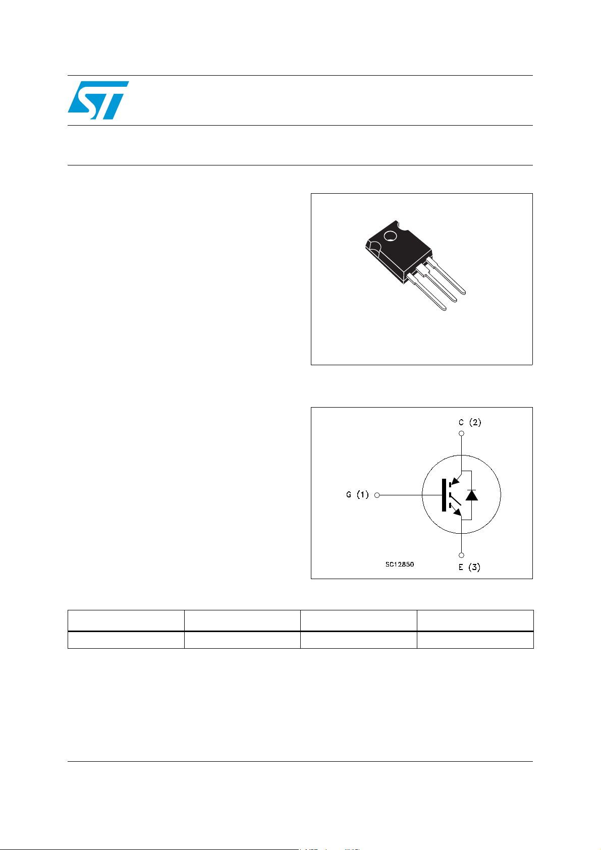
3
2
1
TO-247
Figure 1. Internal schematic diagram
Table 1. Device summary
Order code Marking Package Packaging
STGW30NC60WD GW30NC60WD TO-247 Tube
November 2008 Rev 5 1/14
www.st.com
14

Contents STGW30NC60WD
Contents
1 Electrical ratings . . . . . . . . . . . . . . . . . . . . . . . . . . . . . . . . . . . . . . . . . . . . 3
2 Electrical characteristics . . . . . . . . . . . . . . . . . . . . . . . . . . . . . . . . . . . . . 4
2.1 Electrical characteristics (curves) . . . . . . . . . . . . . . . . . . . . . . . . . . . . . 7
3 Test circuit . . . . . . . . . . . . . . . . . . . . . . . . . . . . . . . . . . . . . . . . . . . . . . . 10
4 Package mechanical data . . . . . . . . . . . . . . . . . . . . . . . . . . . . . . . . . . . . 11
5 Revision history . . . . . . . . . . . . . . . . . . . . . . . . . . . . . . . . . . . . . . . . . . . 13
2/14
STGW30NC60WD Electrical ratings
1 Electrical ratings
Table 2. Absolute maximum ratings
Symbol Parameter Value Unit
V
CES
I
C
I
C
I
CP
I
CL
V
I
I
FSM
P
TOT
T
T
1. Calculated according to the iterative formula:
2. Pulse width limited by max junction temperature
3. V
CLAMP
Collector-emitter voltage (VGE = 0)
(1)
Collector current (continuous) at 25 °C 60 A
(1)
Collector current (continuous) at 100 °C 30 A
(2)
Collector current (pulsed) 150 A
(3)
Turn-off latching current 150 A
Gate-emitter voltage ± 20 V
GE
Diode RMS forward current at TC = 25 °C
F
Surge not repetitive forward current tp= 10 ms sinusoidal
Total dissipation at TC = 25 °C
Storage temperature
stg
Operating junction temperature
j
--------------------------------------------------------------------------------------------------------- -=
R
thj c–
= 80% (V
ICTC()
), VGE = 15 V, RG = 10 Ω, TJ = 150 °C
CES
T
V
CE sat()max()Tjmax()ICTC
–
jmax()TC
600 V
30 A
120 A
200 W
– 55 to 150 °C
(),()×
Table 3. Thermal resistance
Symbol Parameter Value Unit
R
thj-case
R
thj-amb
Thermal resistance junction-case IGBT max. 0.63 °C/W
Thermal resistance junction-case diode max. 1.5 °C/W
Thermal resistance junction-ambient max. 50 °C/W
3/14

Electrical characteristics STGW30NC60WD
2 Electrical characteristics
(T
= 25 °C unless otherwise specified)
CASE
Table 4. Static electrical characteristics
Symbol Parameter Test conditions Min. Typ. Max. Unit
Collector-emitter
V
(BR)CES
V
CE(sat)
V
GE(th)
I
CES
I
GES
g
breakdown voltage
= 0)
(V
GE
Collector-emitter saturation
voltage
Gate threshold voltage
Collector cut-off current
(V
= 0)
GE
Gate-emitter leakage
current (VCE = 0)
Forward transconductance
fs
= 1 mA
I
C
= 15 V, IC= 20 A
V
GE
= 15V, IC = 20 A,TC= 125 °C
V
GE
V
= VGE, IC = 250µA
CE
V
= 600 V
CE
V
= 600 V, TC = 125 °C
CE
VGE = ±20 V
VCE = 15 V, IC = 20 A
600 V
2.1
2.5 V
1.8
3.75 5.75 V
2501µA
± 100 nA
15 S
Table 5. Dynamic electrical characteristics
Symbol Parameter Test conditions Min. Typ. Max. Unit
V
mA
C
C
C
Q
Q
Q
Input capacitance
ies
Output capacitance
oes
Reverse transfer
res
capacitance
g
Total gate charge
Gate-emitter charge
ge
Gate-collector charge
gc
= 25 V, f = 1 MHz,
V
CE
V
= 0
GE
= 390 V, IC = 20 A,
V
CE
= 15 V,
V
GE
(see Figure 18)
2080
175
52
102
17.5
47
pF
pF
pF
140 nC
nC
nC
4/14

STGW30NC60WD Electrical characteristics
Table 6. Switching on/off (inductive load)
Symbol Parameter Test conditions Min. Typ. Max. Unit
t
d(on)
t
(di/dt)
t
d(on)
t
(di/dt)
t
r(Voff
t
d(off
t
t
r(Voff
t
d(off
t
Turn-on delay time
Current rise time
r
Turn-on current slope
on
Turn-on delay time
Current rise time
r
Turn-on current slope
on
)
Off voltage rise time
)
Turn-off delay time
Current fall time
f
)
Off voltage rise time
)
Turn-off delay time
Current fall time
f
= 390 V, IC = 20 A
V
CC
R
G
= 10 Ω, V
GE
= 15 V,
(see Figure 17)
VCC = 390 V, IC = 20 A
= 10 Ω, V
R
G
T
= 125 °C (see Figure 17)
C
= 390 V, IC = 20 A,
V
CC
= 10 Ω, V
R
GE
GE
GE
= 15 V,
= 15 V
(see Figure 17)
= 390 V, IC = 20 A,
V
CC
= 10 Ω, VGE =15 V,
R
GE
= 125 °C
T
C
(see Figure 17)
29.5
12
1640
29
13.5
1600
19.5
118
27
46
151
38
Table 7. Switching energy (inductive load)
Symbol Parameter Test conditions Min. Typ. Max. Unit
(1)
E
on
E
E
E
on
E
E
1. Eon is the tun-on losses when a typical diode is used in the test circuit in Figure 19. If the IGBT is offered
in a package with a co-pak diode, the co-pack diode is used as external diode. IGBTs & Diode are at the
same temperature (25°C and 125°C). Eon include diode recovery energy.
Turn-on switching losses
Turn-off switching losses
off
Total switching losses
ts
(1)
Turn-on switching losses
Turn-off switching losses
off
Total switching losses
ts
= 390 V, IC = 20 A
V
CC
= 10 Ω, V
R
G
GE
= 15 V,
(see Figure 19)
= 390 V, IC = 20 A
V
CC
= 10 Ω, V
R
G
= 125°C (see Figure 19)
T
C
GE
= 15 V,
305
181
486
455
355
810
ns
ns
A/µs
ns
ns
A/µs
ns
ns
ns
ns
ns
ns
µJ
µJ
µJ
µJ
µJ
µJ
5/14
 Loading...