

Page 1
March 2016
DocID029048 Rev 1
1/37
www.st.com
UM2027
User manual
Inrush current limitation when charging a DC bus capacitor for
IEC 61000-3-3 compliance
Introduction
The STEVAL-IHT008V1 evaluation board limits the inrush current charging a DC bus capacitor so that it
is compliant with the IEC 61000-3-3 standard. This inrush current is based on a soft-start procedure for
the rectifier bridge achieved with a Triac added in series with the mains line, which is controlled through
progressive phase-control during the startup phase.
This solution drastically reduces standby losses as the DC bus can be totally disconnected from the AC
mains when it is not required. The DC bus is easily turned off by turning off the series Triac, without
needing an additional relay to open the circuit in standby.
Steady-state losses are also reduced because NTC resistors, traditionally used to limit inrush current,
are not required; nor are the corresponding relays to bypass them.
This board also demonstrates that AC loads can be driven with an isolated easy-to-design solution by
using the same power supply as the whole system and some opto-transistors which control the AC
switches.
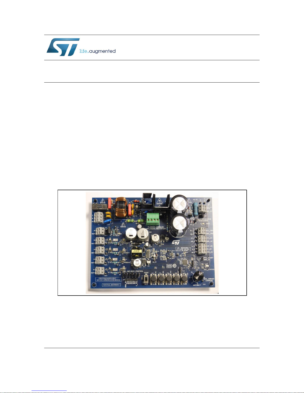
Figure 1: STEVAL-IHT008V1 evaluation board (top view)
Page 2

Contents
UM2027
2/37
DocID029048 Rev 1
Contents
1 Evaluation board objectives .......................................................... 3
1.1 What does this evaluation board aim to demonstrate? .................... 3
1.2 Principal board blocks ...................................................................... 3
1.3 Targeted applications ....................................................................... 4
1.4 Main part numbers ........................................................................... 4
1.5 Operating range and performances ................................................. 5
1.6 Stand-by consumption ..................................................................... 7
2 Getting started ................................................................................ 9
2.1 Safety instruction .............................................................................. 9
2.2 Board connection and start-up ......................................................... 9
2.3 DC bus capacitor discharge for demonstration purpose ................ 10
2.4 LED indications .............................................................................. 10
2.5 Possible board adaptations ............................................................ 11
2.5.1 ACST use and MOV removal .......................................................... 11
2.5.2 EMI filter and DC bus capacitors change ........................................ 11
2.5.3 Power factor circuit connection ....................................................... 12
2.5.4 Motor Inverter connection ................................................................ 12
2.5.5 Control with an external microcontroller .......................................... 12
3 Conclusion .................................................................................... 13
4 STEVAL-IHT008V1 circuit schematics ........................................ 14
5 STEVAL-IHT008V1 power supplies and typical consumption ... 17
6 Inrush-current limitation .............................................................. 19
7 Mains voltage dips and interruptions ......................................... 23
8 AC voltage monitoring and zero-voltage synchronisation ........ 26
9 Triacs and AC switches insulated control .................................. 29
10 EN55014 test results .................................................................... 31
11 STEVAL-IHT008V1 silk-screen .................................................... 32
12 Test points ................................ .................................................... 35
13 Revision history ........................................................................... 36
Page 3

UM2027
Evaluation board objectives
DocID029048 Rev 1
3/37
1 Evaluation board objectives
1.1 What does this evaluation board aim to demonstrate?
This board offers an efficient solution, balancing the following requirements:
Inrush current limitation without inrush current resistor
Standby losses in line with ECO European directive
Low cost and reliable solution to drive AC loads using a single MCU and referenced to
the DC bus ground
The STEVAL-IHT008V1 board is designed to demonstrate these criteria independently;
you only need to connect the AC loads to check this part.
The STEVAL-IHT008V1 board is also intended as a development tool for designers who
want to design a whole system (appliance, air conditioning system, telecom power supply,
etc.).
For this purpose, connectors are available to add an external Power Factor Corrector, an
Intelligent Power Module (IPM) or to use an external microcontroller (see Section 2.5:
"Possible board adaptations").
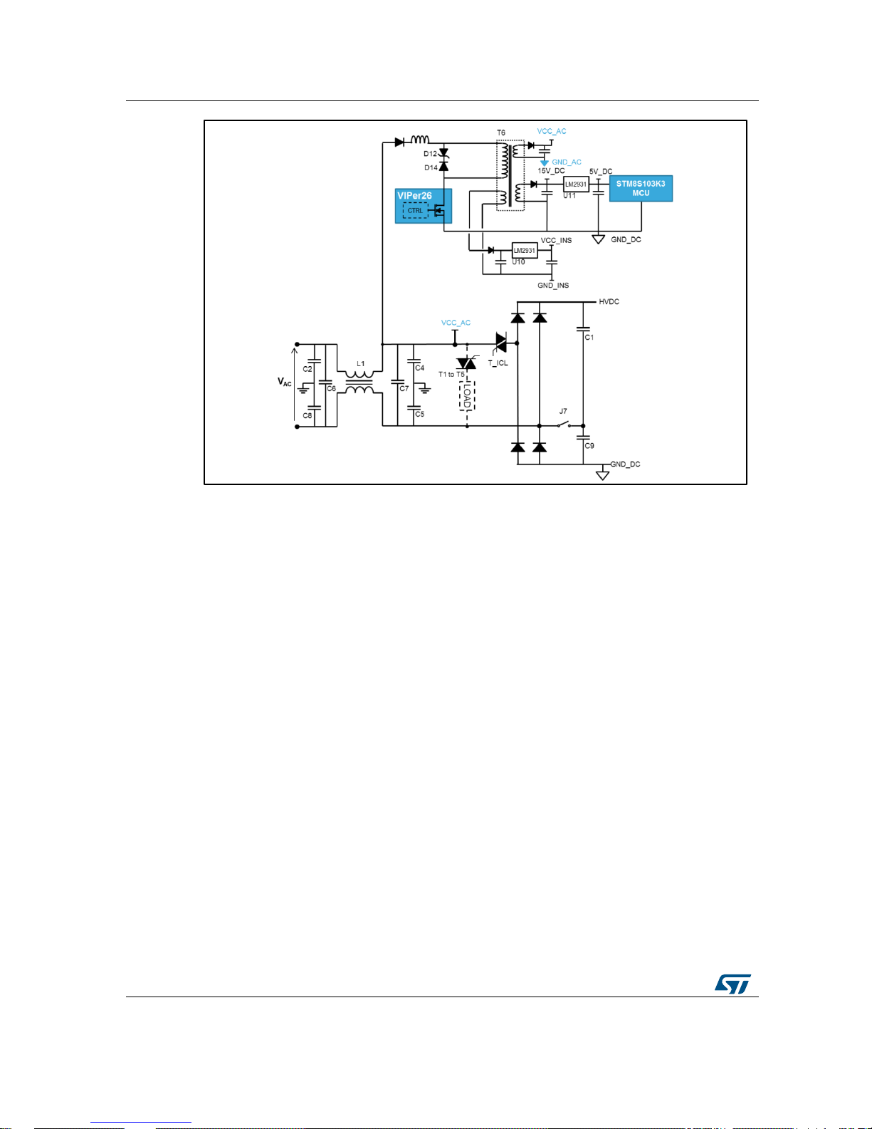
1.2 Principal board blocks
Section 5: "STEVAL-IHT008V1 power supplies and typical consumption" details the
STEVAL-IHT008V1 schematics.
Figure 2: "Board synopsis" summarizes the STEVAL-IHT008V1 board with the following
main components:
The Triac (T_ICL) in series with the diode bridge
The AC switches (T1 to T5) connected on AC side to control AC loads. It should be
noted that their drive reference (A1) is also connected to the A1 terminal of T_ICL. All
A1 terminals are connected to the VCC_AC terminal, allowing this power supply to
provide a trigger current to all AC switches gates.
The MCU, which drives all the AC switches (through opto-transistors, refer to ) and
can also control any supply or motor inverter referenced to the DC bus ground
(GND_DC) in a final application.
The flyback power converter providing:
VCC_AC: 5 V output connected to the Line L1 to implement a negative power
supply. This supply is used for the Triac and AC switches control. Maximum
output current: 200 mA.
5V_DC: 5 V positive output, referenced to the DC bus Ground (GND_DC). This
output supplies the MCU and all the control circuit. Maximum output current: 90
mA.
15V_DC: 15 V positive output, referenced to the DC bus Ground (GND_DC). This
output can be used to supply an IPM to control a three-phase motor in a final
application. Maximum output current: 500 mA (together with 5V_DC
consumption).
VCC_INS: 5 V insulated output. This supply can be used if certain components,
like sensors, must be insulated from the mains voltage. This output is not used in
the demo board. Maximum output current: 90 mA.
For further information on the SMPS outputs, please refer to Section 5: "STEVAL-
IHT008V1 power supplies and typical consumption".
Page 4
Evaluation board objectives
UM2027
4/37
DocID029048 Rev 1
Figure 2: Board synopsis
1.3 Targeted applications
Target applications include all applications using a diode-bridge to rectify the line AC
voltage and require the removal of the NTC (or PTC) resistor and the limitation of standby
losses. Such applications include:
telecom power supplies
televisions, DVD and CD players, set-top boxes, etc.
computers
lighting equipment
This demo board is also particularly interesting for applications where AC loads have to be
controlled, such as for valves, fans, pumps, heating resistors, etc. Such applications
include:
wet appliances (washing machines; dish machines; laundry dryers)
cold appliances (fridges, freezers)
air conditioning units
1.4 Main part numbers
The main part number references used in this demo board are:
Microcontroller Unit (MCU): STM8S103K3
Flyback IC: VIPER26LD
Inrush current limiter Triac: T1635T-8FP or ACST1635-8FP (pin-to-pin compatible with
T1635T-8FP, SIOV1 can be removed)
AC loads AC switches:
T1: ACST210-8FP (TO-220FPAB package)
T2 and T3: ACS108-8SN (SOT223 package)
Page 5

UM2027
Evaluation board objectives
DocID029048 Rev 1
5/37
T4 and T5: Z0109MUF (SMD package)
1.5 Operating range and performances
The STEVAL-IHT008V1 board is designed to operate inside the following operating ranges:
Line voltage, 2 ranges are possible:
198-264 V RMS, 50 or 60 Hz
90-132 V RMS, 50 or 60 Hz. For this voltage range, operation both in rectifier
mode (DC peak voltage = peak line voltage) or in doubler mode are possible (see
Section 2.2: "Board connection and start-up").
Ambient temperature: 0°C to 60°C
Maximum DC load power:
DC load (connected between HVDC and GND-DC): 1000 W or 500 W
respectively for operation on 230 V or 120 V mains.
Maximum AC load power:
T1: maximum load RMS current has to be lower than 1.1 A, this allows 250 VA or
130 VA power for operation on 230 V or 120 V mains, respectively. This Triac
can be used to control a heating resistor or a pump.
T2 to T5: the footprint for each of these devices allow either a SMBflat-3L or a
SOT-223 package to be soldered. By default, two ACS108-8SN (SOT-223) are
used for T2 and T3, with a 5.5 mm² copper area under the tab. These devices
can control an RMS load current up to 0.6 A. This allows a 100 VA or 50 VA
power load to be controlled on 230 V or 120 V mains, respectively. By default,
two Z0109MUF (SMBflat-3L) are used for T4 and T5, with a 33.6 mm² copper
area under the tab. These devices can control an RMS load current up to 0.44 A.
This allows a 140 VA or 70 VA power load to be controlled on 230 V or 120 V
mains, respectively. These four Triacs can be used to control a pump, a fan or
any electromagnet (valve, damper, door-lock, etc.).
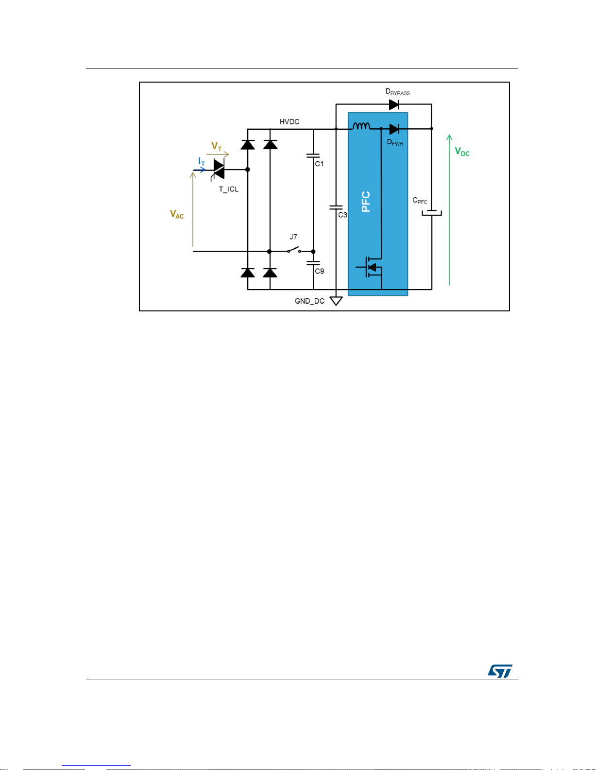
Allowed DC output capacitor (or DC bus capacitor) range: 50 µF to 500 µF (in rectifier
mode) or to 1000 µF (in doubler mode).
This DC output capacitor value is the equivalent value of all capacitors placed in
parallel at the bridge output, like C1, C9, C3, and CPFC at PFC output (refer to
Figure 3: "Connection of a PFC at the HVDC output"). If an interleaved PFC is
used, all the output capacitors of each PFC must be added.
If the J7 connector is closed (doubler mode), no PFC should be used. C3 is also
not added. In this case, the equivalent capacitor is only C1 (or C9 as they both
have the same value).
Page 6
Evaluation board objectives
UM2027
6/37
DocID029048 Rev 1
Figure 3: Connection of a PFC at the HVDC output
The main STEVAL-IHT008V1 board performance characteristics are:
Efficiency at 230 V 50 Hz 1000 W (only DC resistive load) = 97%
Efficiency at 120 V 60 Hz 500 W (only resistive DC load, rectifier or double modes) =
96%
Standby losses < 150 mW (refer also to section 2.6)
Compliance with IEC 61000-3-3 (with potentiometer "MAX_INRUSH CURRENT" set
to default position; refer to Section 6: "Inrush-current limitation")
Compliance with EN55014 (CIPSPR 22 method B; refer to Section 10: "EN55014 test
results")
IEC 61000-4-4: 2 kV criteria A, T_ICL Triac withstands a 5 kV level without triggering.
This is to avoid undesirable triggering and uncontrolled inrush current due to EMI
noise.
IEC 61000-4-5: 2 kV criteria A
IEC61000-4-11: criteria A for dips down to 100% of the line voltage during 1 cycle;
criteria B for interrupts up to 300 cycles or more (refer to Section 7: "Mains voltage
dips and interruptions").
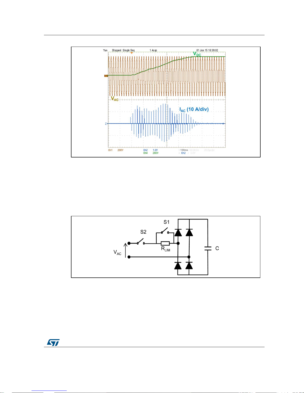
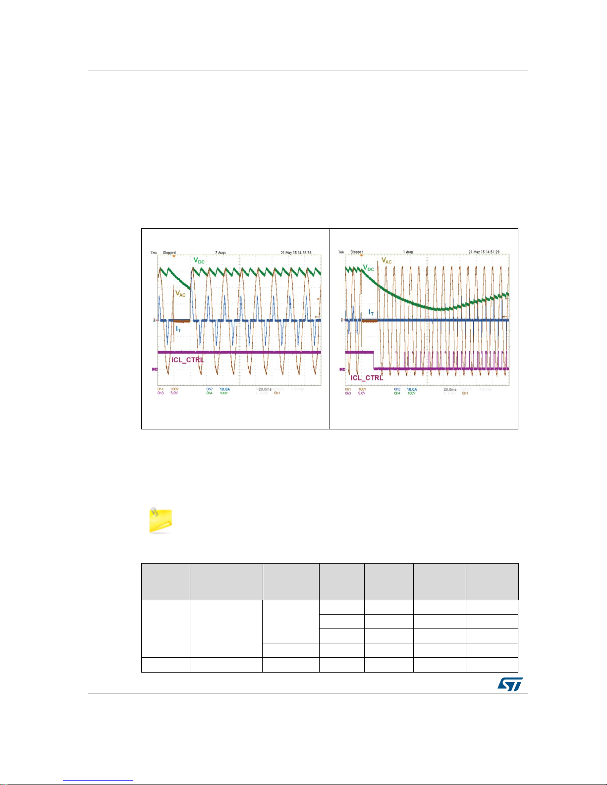
Figure 4: "Inrush current at STEVAL-IHT008V1 startup on 230 V line (500 µF output DC
capacitor)" shows an example of the progressive DC capacitor charge ensured by the
T_ICL Triac. The test is performed at startup when the STEVAL-IHT008V1 board is
connected to a 230 V 50 Hz grid, while the output DC capacitor is completely uncharged
(initial voltage is zero). The output DC capacitor is implemented in this case via the series
association of C1 and C9, hence the equivalent capacitance is 500 µF.
The output capacitor is charged in 550 ms with the input RMS current remaining far below
the 16.1 A limit. IEC 61000-3-3 compliance is therefore easily achieved.
Page 7
UM2027
Evaluation board objectives
DocID029048 Rev 1
7/37
Figure 4: Inrush current at STEVAL-IHT008V1 startup on 230 V line (500 µF output DC
capacitor)
1.6 Stand-by consumption
One of the main advantages of using the T_ICL Triac in front of the rectifier bridge is that it
allows full bridge disconnection during standby to suppress losses. This can also be
achieved by adding a front-end relay (like S2 in Figure 5: "Solution using relays to limit
inrush current and standby losses"). But, thanks to the T_ICL Triac, this function is already
available by simply turning off this Triac.
Figure 5: Solution using relays to limit inrush current and standby losses
To give an idea of the benefits of such bridge disconnection, we measured the typical
losses of the STEVAL-IHT008V1 board in standby mode. Three cases are tested:
Case 1: STEVAL-IHT008V1 board (unmodified) with T_ICL in OFF state ("HVDC"
switch in OFF position).
Case 2: as above, but with a PTC (EPCOS B59107J0130A020) plugged in place of
the T_ICL Triac to simulate the losses for a classic solution using only one PTC and
Page 8
Evaluation board objectives
UM2027
8/37
DocID029048 Rev 1
one bypass relay (refer to RLIM and S1 on Figure 5: "Solution using relays to limit
inrush current and standby losses").
Case 3: as above, but circuits used solely for demonstration purposes and which
consume undesired power at standby are disconnected. These circuits are the "HV
Capacitor Discharge" circuit (where R7 and R10 are connected to the DC bus) and the
"HVDC" LED (D2) indicating presence of high voltage (where D1, R12, and R13 are
connected to the DC bus).
Table 1: "Comparison of standby losses" gives the experimental results for the three cases
in the three different modes of operation (230 V, 110 V line voltage in rectifier and doubler
mode). The tests results clearly show that the Triac solution is the only one to achieve a
power consumption level lower than 0.5 W, as currently required by European directive
2005/32/EC.
The losses measured for case 3 are mainly due to the resistor divider circuit (R9, R11,
R14, R16) used to balance the voltage across the 2 series capacitors (C1 and C9) and the
other resistor divider circuit (R30, R31) used to sense the HVDC voltage. On our board, the
HVDC voltage is monitored to check proper soft-start operation and to avoid that the DC
capacitor charge duration is too long (if, for example, a load remains connected to the DC
bus before start-up). In standard circuits, however, such a voltage sensor is often required
(to start the PFC or the DC-DC supplies, for example).
The losses for a 230 V rectified voltage equal 520 mW for the 200 kΩ R9, R11, R14 and
R16 equivalent resistor, and 52 mW for the 2 MΩ R30 and R31 equivalent resistor.
Table 1: Comparison of standby losses
Mode of
operation
Case 1
T_ICL OFF
Case 2
PTC instead of Triac
Case 3
PTC discharge and D2 LED
circuits removed
230 V
125 mW
1.7 W
950 mW
110 V / rectifier
mode
70 mW
0.6 W
280 mW
110 V / doubler
mode
70 mW
1.5 W
860 mW
Page 9
UM2027
Getting started
DocID029048 Rev 1
9/37
2 Getting started
2.1 Safety instruction
The high voltage levels used to operate the STEVAL-IHT008V1 evaluation board
can represent a serious electrical shock hazard. This evaluation board must be
used in a suitable laboratory only by qualified personnel who are familiar with the
installation, use, and maintenance of power electrical systems.
The STEVAL-IHT008V1 evaluation board is designed for demonstration purposes only,
and must never be used for either domestic or industrial installations.
2.2 Board connection and start-up
Please follow this procedure to use the STEVAL-IHT008V1 board:
1. If you want to operate the board on a 98-132 V line voltage and have a DC bus
voltage two times higher than the peak line voltage, plug the jumper (see Figure 6: "(a)
J7 jumper plugged on board (doubler mode)") to the position indicated by the silk-
screen (refer to Figure 7: "(b) Jumper position left free (rectifier mode)"). If you want
the rectifier to operate in a classic rectifier circuit, do not plug the J7 jumper.
2. Connect the AC load terminals (if used) to the associated headers (e.g., for AC switch
T1, refer to the "N1-OUT1" label in Figure 23: "STEVAL-IHT008V1 silk-screen (Top
side)").
3. Connect the L, N and PE (if required) of J9 header to an unpowered mains plug.
4. Apply the mains voltage. From this moment on, avoid any contact with live parts
subject to line voltage.
5. Switch the "HVDC ON" toggle button to the "ON" position" to start charging the DC
capacitors.
6. The AC loads are switched on and off each time the associated push-buttons (T1 to
T5) are pressed. These loads are controlled even if the "HVDC ON" button is kept in
the OFF position.
7. The rate of DC capacitor charging can be increased if the allowed peak current is
increased. To do this, turn the "MAX-INRUSH CURRENT" potentiometer clockwise.
compliance with the IEC 61000-3-3 standard is only guaranteed when th
potentiometer is set to the default position (between 0 and 1 mark) and with
original values of the EMI filter and output DC capacitors.
The following figures show the J7 jumper connection for doubler mode (a) or rectifier mode
(b).
Page 10
Getting started
UM2027
10/37
DocID029048 Rev 1
Figure 6: (a) J7 jumper plugged on board
(doubler mode)
Figure 7: (b) Jumper position left free
(rectifier mode)
2.3 DC bus capacitor discharge for demonstration purpose
With default STEVAL-IHT008V1 1000 µF output capacitors (C1, C5) and associated 50 kΩ
resistors (R9, R11, R14, R16) used in parallel to balance the voltage across the two series
capacitor, the DC bus discharging time takes a few minutes if no load is connected.
A circuit is included to accelerate this discharging time, especially if several startups need
to be performed inside a short time interval for test or demonstration purposes. This circuit
is made with the Q2 MOSFET and R8 Resistor. Q2 remains on for as long as the SW7
SPDT toggle (refer to the "HV CAPACITOR DISCHARGE" label in Figure 23: "STEVAL-
IHT008V1 silk-screen (Top side)") is switched to the momentary ON position.
The two 1000 µF capacitors are then discharged within two seconds, approximately. The
SW2 switch must at least be kept in the momentary ON position during these two seconds.
The D2 LED (refer to the "HVDC" label in Figure 23: "STEVAL-IHT008V1 silk-screen (Top
side)") remains lit while the HVDC voltage is above 50 V, so the SW2 switch can be
released and a new startup can begin as soon as this LED turns off.
2.4 LED indications
Several LEDs are available to signal useful information:
ICL-STATUS" (LED D18): indicates several things according to its color:
When the board is powered, the LED passes from red, to orange, to green, which
indicates that the microcontroller has finished startup (correct mains connection
and line frequency measurement, power supply available, etc.) and the board is
ready. The green LED then switches off to reduce the board consumption in
standby. From this moment, the DC output capacitor can be charged when the
"HVDC" switch (SW6) is set to the "ON" position.
Green flashing indicates the DC bus capacitors are charging (flashing starts after
setting the "HVDC" button to the ON position and ends when the DC bus
capacitors are fully charged). This flashing mode can last less than 1 second and
may therefore go undetected by the end-user.
Green constant indicates the DC bus is charged to the correct voltage.
Orange flashing indicates the DC bus capacitors are charging but the output DC
voltage rate of increase is too low. This may occur if a power load is connected to
Page 11
UM2027
Getting started
DocID029048 Rev 1
11/37
the HVDC bus during charging and sinks a current which is too high, preventing
the DC capacitor from being charged efficiently.
Orange constant indicates the output DC capacitor is not charged to the peak line
voltage. This may occur when the bridge is started, but a power load is already
connected to the HVDC bus and sinks a current which is too high, preventing the
DC capacitor from being fully charged.
Red constant indicates the board is connected to a 198-264 V line while the
doubler jumper is connected.
Red flashing indicates the MCU detected an error (e:g., the line voltage is outside
the two correct operating ranges: 90-132 V and 198-264 V; the line frequency is
not detected as stable for 50 or 60 Hz).
"HVDC" (LED2): this LED lights red when a voltage higher than 50 V is present
between HVDC and GND_DC terminals (refer to Section 2.3: "DC bus capacitor
discharge for demonstration purpose" for further information).
"OUT1" to "OUT5" (LED6 to LED10) are ON when the corresponding AC switch (T1 to
T5) is turned on.
2.5 Possible board adaptations
The STEVAL-IHT008V1 board allows certain external components to be added to the frontend circuit, so designers can validate an entire system. The main possible modifications
are listed below.
2.5.1 ACST use and MOV removal
The T1635T-8FP Triac used for T_ICL can be replaced by an ACST1635-8FP. Both
devices are indeed pin-to-pin compatible. The MOV used to protect the T1635T-8FP
(SIOV1) can be removed as the ACST1635T is an overvoltage protected device.
if the ACST1635-8FP is triggered in breakover mode, the applied current and its
rate of increase (di/dt) must remain below the values specified in the datasheet:
290 A peak current (8/20 µs waveform) and 150 A/µs, respectively.
For a high output DC capacitor value, the current may exceed this datasheet limit.
On our board, the input varistor (SIOV2) clamps the voltage applied to the ACST1635-8FP
below the typical clamping voltage of the device (VCL) for surges up to 2 kV. This prevents
ACST1635-8FP turn-on in breakover.
2.5.2 EMI filter and DC bus capacitors change
The EMI filter and DC capacitors only use through-hole devices to facilitate unsoldering
them to replacing them with ones used in the target application. This allows a designer to
adapt the EMI filter and HVDC voltage ripple to specific application requirements (such as
the power rating).
Obviously, as soon as these component values are modified, the control law of the T_ICL
Triac has to be updated to ensure ongoing compliance with the IEC 61000-3-3 limits. For
this purpose, the maximum peak current during startup can be adjusted with the "MAXINRUSH CURRENT" potentiometer. When this potentiometer is turned clockwise, the Triac
is turned sooner at each half-cycle, leading to a higher peak current.
The maximum RMS current or voltage fluctuation (when a normalized line impedance is
used) must then be measured according to the potentiometer position to check compliance
with IEC 61000-3-3.
Page 12

Getting started
UM2027
12/37
DocID029048 Rev 1
if the EMI filter capacitors (C3, C4, C44 to C47) values are increased, the values
of R9, R11, R14 and R16 may be decreased so the capacitors can still discharge
to below a safe voltage level (120 V for a DC voltage) in less than one or two
seconds. Indeed the EMI filter capacitors voltage is applied to the power plug
when the board is unplugged, so power terminals with accessible live parts
represent an electric shock hazard.
2.5.3 Power factor circuit connection
A PFC can be connected on the HVDC bus through the HVDC and GND_DC connections
(J12 header). To ensure the correct operation of this PFC circuit, capacitors C1 and C9
must be unsoldered. C3 (no capacitor is soldered here by default) may be used to add a
630 V DC film capacitor.
As the T_ICL Triac is controlled by a DC gate current when the HVDC voltage has reached
its steady-state value, either a discontinuous mode or a continuous mode PFC can be
used.
For correct operation of the STEVAL-IHT008V1 front-end circuit with a PFC, the PFC must
be activated after the "PFC_START" signal has been set to a 5 V high level. This signal is
referenced to the GND_DC terminal. It is available through the J20 header.
the PFC DC storage capacitor (ref. CPFC in Figure 3: "Connection of a PFC at
the HVDC output") has to within the value range defined in Section 1.5:
"Operating range and performances".
2.5.4 Motor Inverter connection
An inverter or any other DC-DC power converter can be added after the PFC or directly
behind the HVDC bus output.
A 15 V positive output referenced to the DC Bus Ground (GND_DC) is available through
header J10 to supply an IPM module if needed. Ensure that the maximum current which is
sunk from this supply is well below the limit given in Figure 12: "Typical output
characteristics of the 5 V and 15 V positive supplies (5V_DC / 15V_DC)".
2.5.5 Control with an external microcontroller
It is possible to control the STEVAL-IHT008V1 front-end circuit with an external MCU,
instead of using the embedded STM8S103K3. This allows the end-user to directly check
the compliance of his or her own firmware with this kind of circuit.
For this purpose, all control signals required to drive the different AC switches are available
on the J16 header. EC1 to EC5 are the external control signals of AC switches T1 to T5;
T_ICL is the connection to externally drive the T_ICL Triac. The GND_DC and ZVS signals
are also available on this header to synchronize the control signals of the external MCU.
For correct operation with external signals, jumpers J1 to J6 (refer to the
"INT/EXT_CONTROL" label Figure 23: "STEVAL-IHT008V1 silk-screen (Top side)") must
be removed. The removal of these jumpers indeed allows the disconnection of the optotransistor input LEDs from the U9 microcontroller outputs (Figure 8: "STEVAL-IHT008V1
power side and insulated control schematic").
Page 13

UM2027
Conclusion
DocID029048 Rev 1
13/37
3 Conclusion
This evaluation provides an innovative front-end circuit to allow both inrush current
limitation and power loss reduction. Above and beyond the simple demonstration of the
efficiency and the robustness of this solution by STMicroelectronics, this front-end circuit
also represents the starting point for building entire system and accelerating the time-tomarket of new application designs.
Page 14

STEVAL-IHT008V1 circuit schematics
UM2027
14/37
DocID029048 Rev 1
4 STEVAL-IHT008V1 circuit schematics
Figure 8: STEVAL-IHT008V1 power side and insulated control schematic
Page 15
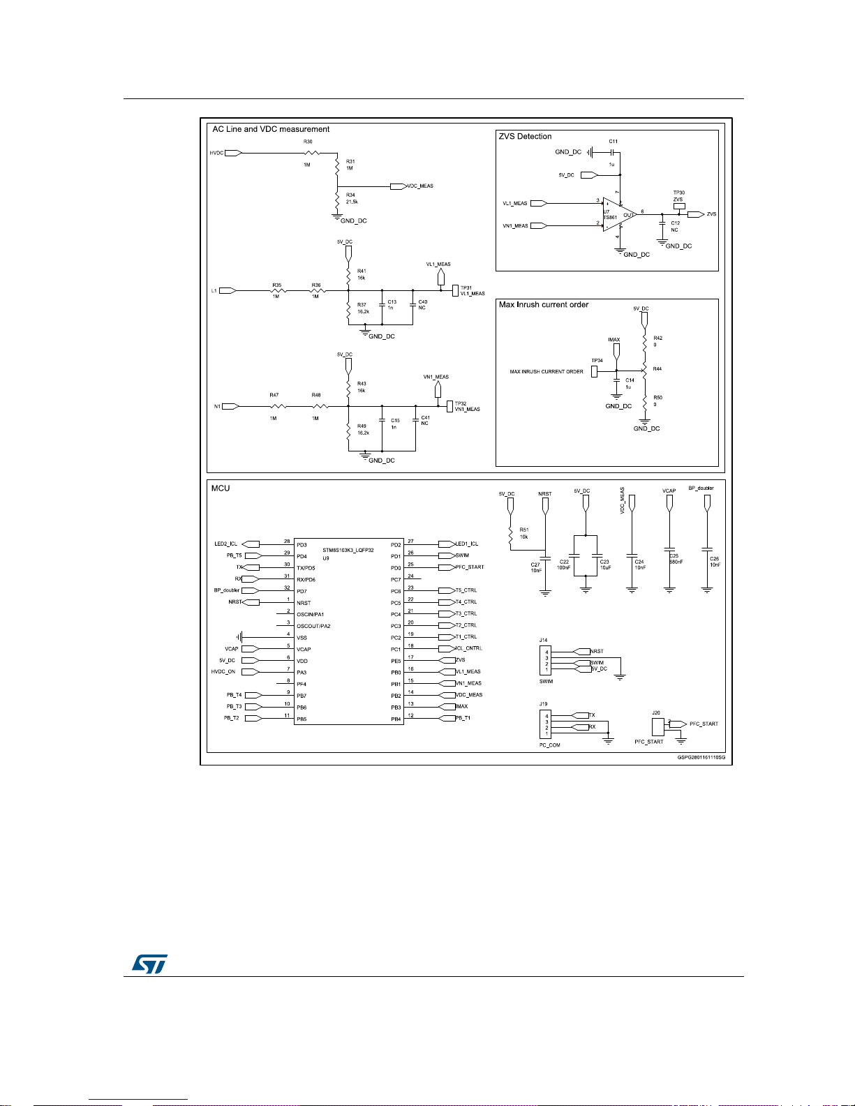
UM2027
STEVAL-IHT008V1 circuit schematics
DocID029048 Rev 1
15/37
Figure 9: STEVAL-IHT008V1 control circuit schematic (1 of 3)
Page 16

STEVAL-IHT008V1 circuit schematics
UM2027
16/37
DocID029048 Rev 1
Figure 10: STEVAL-IHT008V1 control circuit schematic (2 of 3)
Figure 11: STEVAL-IHT008V1 control circuit schematic (3 of 3)
Page 17

UM2027
STEVAL-IHT008V1 power supplies and typical
consumption
DocID029048 Rev 1
17/37
5 STEVAL-IHT008V1 power supplies and typical
consumption
Table 2: "Typical STEVAL-IHT008V1 control-circuit consumption" gives the typical current
consumed from the 5V_DC output for the different operating modes of the STEVALIHT008V1 board.
Table 2: Typical STEVAL-IHT008V1 control-circuit consumption
Operating mode
Current sunk from 5V_DC (mA)
MCU in standby mode
2
MCU running with 1 ACS switch ON (T2 to T5)
14
MCU running with T_ICL ON
17
MCU running with T_ICL and 1 ACS switch ON
24
MCU running with T_ICL and 4 ACS switches ON
45
As listed in Section 1.2: "Principal board blocks", the Flyback implements four output
supplies. The non-regulated 5 V VCC_AC negative supply is used for the Triac and ACS
control. The 15 V and 5 V positive supplies (15V_DC and 5V_DC outputs) are used to
supply circuits referenced to the DC bus Ground (MCU, IPM if one is added).
The 5 V insulated supply (VCC_INS / GND_INS) can be used for sensors if needed. On
original STEVAL-IHT008V1 manufactured boards, this insulated supply is not used.
Only the 15 V positive output is regulated by the VIPer26LD circuit as this supply is always
loaded when the other outputs are loaded. The two 5 V positive supplies (5V_DC,
VCC_INS) are also regulated thanks to two LM2931 positive voltage regulators.
The VCC_AC level is not regulated. Its voltage level will be higher if it is not loaded and if
the 15 V positive supply is loaded with its highest maximum current.
The current capabilities of the different outputs are (for the whole operating range):
for 5V_DC: 90 mA
for VCC_AC (non-regulated 5 V negative output): 200 mA
for 15V_DC: 500 mA (with 5V_DC consumption included)
for VCC_INS (optional 5 V regulated output): 90 mA
Figure 13: "Typical output characteristics of the 5 V negative supply (VCC_AC) and 5 V
insulated supply (VCC_INS)" and Figure 14: "Inrush current during STEVAL-IHT008V1
startup on 230 V line (500 µF output DC capacitor)" give the typical output voltage for the
current which is sunk from each output. These measurements are performed with the
STEVAL-IHT008V1 connected to either a 230 V or 120 V line, with the bridge operating in
rectifier mode (not doubler) and across the entire operating temperature range (0-60 °C).
The 15 V_DC, and the 5 V outputs (5V_DC and VCC_INS) are well regulated thanks to the
VIPer26LD and the LM2931 devices, respectively.
For the VCC_AC, two curves are given to give the minimum and maximum values of this
output. The minimum voltage is reached when the SMPS is delivering the minimum output
current (no current sunk from the 15V_DC and the VCC_INS outputs; the 5V_DC is only
loaded by the MCU, which is controlling one ACS ON).
The VCC_AC measurement is also performed when only one ACS switch is ON as
VCC_AC is dedicated to the Triac and ACS switches driving. So the minimum available
voltage (to define the gate resistor value to apply enough gate current) is an important
value, at least when one AC switch is on.
Page 18

STEVAL-IHT008V1 power supplies and typical
consumption
UM2027
18/37
DocID029048 Rev 1
For Figure 14: "Inrush current during STEVAL-IHT008V1 startup on 230 V line
(500 µF output DC capacitor)", the output current of the horizontal axis gives the
extra current sunk from the output voltage when one ACS switch is ON. This
means that for a zero current, a current close to 20 mA is already sunk from the
VCC_AC supply. This is not the case for the VCC_INS output.
The maximum VCC_AC voltage is reached when the SMPS 15V_DC output is loaded to
the maximum output current (500 mA), while only one AC switch is ON. Indeed if more
ACS switch gate currents are sunk from VCC_AC, this level decreases.
Figure 12: Typical output characteristics of the 5 V and 15 V positive supplies (5V_DC /
15V_DC)
Figure 13: Typical output characteristics of the 5 V negative supply (VCC_AC) and 5 V
insulated supply (VCC_INS)
Page 19

UM2027
Inrush-current limitation
DocID029048 Rev 1
19/37
6 Inrush-current limitation
IEC 61000-3-3 standard reminder
The IEC 61000-3-3 standard gives the limitation of voltage changes and fluctuations for
equipment with rated RMS current lower than 16 A connected to a public low-voltage grid.
These voltage fluctuations are indeed caused by the equipment if too high a current is sunk
from the grid. A voltage drop is then caused due to the line impedance.
The mains voltage fluctuation causes an undesirable variation in the brightness of lamps
and displays; namely, the flicker phenomenon. This is why designers must keep the inrush
current sunk by their equipment to below specific limits.
The following equation explains the link between the line current variation I
input
(due to the
equipment operation) and the relative mains voltage variation (U), which must be lower
than the maximum allowed value (d
max
given in %).
U = I
input
x Z
ref
/ U x 100 < d
max
where Z
ref
is the normalized line impedance (0.6 with 796 µH in series for a single-phase
grid) and U is the nominal RMS line voltage.
The d
max
level should not exceed 4%. A 6% or 7% limit is also allowed according to the way
the equipment is switched (manually or automatically, delayed or not, etc.) or for specific
appliances.
If the U variation exceeds 3.3% during a single voltage change, this should not last more
than 500 ms.
Table 3: "Maximum input RMS current variation for 230 V single-phase grid according to
IEC 61000-3-3" gives the associated maximum input current variation related to these
different d
max
levels. To simplify the analysis, it could be said that an appliance will fulfill
with the IEC 61000-3-3 limit at startup if its RMS current remains below 16.1 A. The relative
variation is thus lower than 3.3% and compliance is ensured even if startup lasts more than
500 ms. It is clear that this is a restricted case for simplification purposes, higher current
variations may also still allow compliance with this standard.
Table 3: Maximum input RMS current variation for 230 V single-phase grid according to IEC
61000-3-3
d
max
(%)
DU (V)
DI
input
(A)
3.3
7.6
16.1
4
9.2
19.5
6
13.8
29.3
7
16.1
34.1
STEVAL-IHT008V1 compliance with the IEC 61000-3-3 limit
Currently, one of the most used solutions to limit inrush current consists of adding a resistor
(refer to RLIM in Figure 5: "Solution using relays to limit inrush current and standby losses")
in series with the DC capacitor (refer to C). This resistor must then be bypassed to limit
power losses during steady-state operation. Usually, a relay or a Triac (S1) is used for this
purpose. To disconnect the DC bus during standby mode, a second switch (S2) is required.
To avoid the use of the RLIM resistor, a different startup procedure can be implemented.
With the Triac T_ICL placed in series with the diode bridge, the capacitor can be charged
smoothly through progressive phase control. As long as the Triac is not triggered, the
bridge does not conduct any current, and the DC bus capacitor is not charged. To start
Page 20

Inrush-current limitation
UM2027
20/37
DocID029048 Rev 1
charging the DC capacitor, the Triac must be turned on. To reduce the inrush current, the
Triac is first triggered at the end of the line voltage cycle, just a few hundred microseconds
before the line zero voltage. This allows the output capacitor (refer to C in Figure 5:
"Solution using relays to limit inrush current and standby losses") to be charged to a low
level (around 10 to 30 V) and not directly to the peak line voltage. The current driven from
the line is then much lower than in case of directly charging the DC capacitor completely.
This soft-start solution can only work when an inductor is present on the line side as the
current increase rate must also be limited to avoid Triac damage. Such an inductor is
already present for most applications where the EMI filter usually embeds a common-mode
choke which has a differential-mode parasitic inductor due to the copper turns of the
windings.
In our STEVAL-IHT008V1, the EMI filter is implemented by C6-C7 X2 capacitors, C2-C4C5-C8 Y2 capacitors, and the L1 common-mode inductor. This inductor features a 12 mH
value in common-mode but also a 10 µH inductor in differential mode. This is the
differential-mode value which allows the reduction of the rate of increase of the line current
each time Triac T_ICL is turned on.
To allow a complete charge of this capacitor to the peak line voltage, the Triac must be
triggered on the following cycle with a shorter turn-on delay than the first one used to start
the charge. In this way, by reducing the Triac turn-on delay by a few tens or hundreds of
microseconds from half-cycle to half-cycle, the output capacitor is progressively charged
while the line current is kept low.
In the STEVAL_IHT008V1 MCU firmware, the Triac turn-on delay reduction step is
constant from one half-cycle to the following one. This step is called
Step_Phase_Control in the firmware. It is set by the Max_Inrush_Current_Order
routine which reads the voltages set by the "MAX_INRUSH CURRENT" potentiometer.
When the T_ICL Triac turn-on delay is lower than 3 ms, the gate pulse is directly set to a
continuous DC pulse (starting typically 70 µs after VAC zero voltage). Indeed, below a
delay of approximately 5 ms or 4.2 ms (for 50 and 60 Hz line frequencies, respectively), the
output DC capacitor is fully charged. Therefore, it is not necessary to ensure a soft start for
turn-on delays much lower than a fourth cycle.
the max T_ICL turn-on delay is defined by the ICL_CTRL_Delay in the
firmware. The minimum value of 3 ms is defined by the
Phase_Control_ON_Max which sets the maximum T_ICL ON time (7 ms, refer
to directive definitions in the firmware).
Figure 14: "Inrush current during STEVAL-IHT008V1 startup on 230 V line (500 µF output
DC capacitor)" (same as Figure 4: "Inrush current at STEVAL-IHT008V1 startup on 230 V
line (500 µF output DC capacitor)") shows an example of such progressive DC capacitor
charging. The test is performed at startup when the STEVAL-IHT008V1 board is connected
to a 230 V 50 Hz grid, while the output DC capacitor is completely uncharged (i.e., its initial
voltage is null). The output DC capacitor is implemented in this case by the series
association of C1 and C9 for an equivalent capacitance of 500 µF.
the electric parameters of Figure 15: "Triac current zoom for the highest peak
current during start-up" are defined in Figure 3: "Connection of a PFC at the
HVDC output" (arrow head gives the hot-point of the voltage). In Figure 3:
"Connection of a PFC at the HVDC output", VDC is actually the voltage across
capacitor C3 as no PFC is used.
Page 21

UM2027
Inrush-current limitation
DocID029048 Rev 1
21/37
Figure 14: Inrush current during STEVAL-IHT008V1 startup on 230 V line (500 µF output DC
capacitor)
Here, the MCU firmware is the default program, so:
the first T_ICL turn-on is set to 410 µs before next line Zero Voltage. As the first gate
current pulse lasts 50 µs, the gate current can be removed 360 µs before the next half
cycle and avoid full-wave conduction in the next half-cycle.
This 360 µs interval includes the ZVS signal delay (which can equal up to 70 µs, see
Section 8: "AC voltage monitoring and zero-voltage synchronisation"), the MCU data
treatment time before setting the ICL_CTRL I/O pin to high (40 µs) and the delay
required transistor Q3 to become unsaturated, which drives T_ICL (150 µs). The total
delay time therefore equals 260 µs; 150 µs is added as the safety margin. This delay
is called ICL_TRIAC_OFF_Delay in the firmware. As the timer is launched both in
count-up and count-down modes, half of the desired value must be given in this
parameter.
Next T_ICL turn-on occurs 50 µs sooner each time when the "MAX_INRUSH
CURRENT" potentiometer is set to the DEFAULT position. This minimum step value is
defined in the directive section of the firmware (Step_Phase_Control_Min).
the DEFAULT position corresponds to the slowest output DC capacitor charge
and therefore the shortest Step_Phase_Control value. When the
"MAX_INRUSH CURRENT" potentiometer is turned clockwise after point 1,
Step_Phase_Control increases roughly linearly from around 50 µs (position
1) to 600 µs (position 6).
When the T_ICL Triac turn-on delay goes lower than 3 ms, the Triac is triggered by a
DC gate current.
Figure 15: "Triac current zoom for the highest peak current during start-up" shows that, in
these conditions, the inrush peak current remains below 17.4 A. The RMS current is thus
far below the 16.1 A limit (as explained below). This means that the relative variation is
lower than 3.3%. It is therefore not necessary to check the duration of the accumulated
Page 22

Inrush-current limitation
UM2027
22/37
DocID029048 Rev 1
time of deviation exceeding 3.3%. Here, the output capacitor is charged in 550 ms and
compliance with IEC 61000-3-3 is achieved.
It should also be noted that the peak current during output capacitor charge is not constant.
Indeed, only the step of the reduction of the T_ICL Triac turn-on delay is constant. Hence,
depending on when this Triac turns on, the peak current can vary slightly from one period
to another.
It can also be noted that we have limited the inrush peak current to below 17.4 A, but the
IEC 61000-3-3 limit actually applies to the RMS current. As the T_ICL Triac conducts for a
few hundred microseconds each half-cycle, the RMS current is much lower than the peak
value. Figure 16: "(a) Board operation during 1-cycle line interruption" gives of a zoom of
the Triac current for the highest peak current event measured in Figure 15: "Triac current
zoom for the highest peak current during start-up". The Triac conduction lasts 560 µs, its
RMS current equals then 2.45 A, which is much lower than the measured 17.4 A peak
current.
This figure also shows that the output DC voltage is increased by 12 V during this single
Triac conduction.
Figure 15: Triac current zoom for the highest peak current during start-up
Page 23

UM2027
Mains voltage dips and interruptions
DocID029048 Rev 1
23/37
7 Mains voltage dips and interruptions
IEC 61000-4-11 standard defines the test conditions to evaluate the immunity of equipment
to voltage dips or interruptions. This electromagnetic standard is given as a test method
reference by other standards. For example, product standards like EN55014-2 for
appliances or EN 55024 for IT equipment, which require product compliance in order to be
sold on the European open market, specify the tests to be performed according to IEC
61000-4-11 standard and the expected corresponding tests results.
If a product is not listed in a specific product standard, the general electromagnetic
standard applies according to the use environment (residential or industrial, for example).
As any appliance connected to the mains can be subjected to line voltage dips or
interruptions, a high input current may occur when the line voltage suddenly increases back
to its nominal value to rectifier circuits charging DC capacitors. This high current may
damage the front-end circuit components like the bridge diodes, the AC fuse, etc.
Table 4: "Required dips and interruptions tests and STEVAL-IHT008V1 performance" gives
the different requirements in terms of line voltage dips and interruptions for the different
electromagnetic immunity standards. In summary, the worst cases to account for are:
Voltage dips: 1 cycle with a 0% residual voltage, and 50 cycles with a 70% residual
voltage
Voltage interruptions: 0% residual voltage during 250 or 300 cycles respectively for 50
and 60 Hz line frequency.
A criteria B is requested for the 0% voltage test during 1 cycle, while the other tests require
only a criteria C.
The MCU firmware of the STEVAL-IHT008V1 board is programmed in order to comply with
these different standard tests with the following strategy:
If the line voltage remains higher than 70% to the reference voltage (measured at
board startup), no change applies to all the Triacs (including T_ICL) orders.
If the line voltage falls below 70% of the reference voltage during at least 1.5 cycles,
all the Triacs (including T_ICL) are switched off. The DC bus voltage will be
discharged by its load current. When the line voltage is reapplied, the T_ICL Triac is
controlled in soft-start again to ensure recharging current limitation. It is clear that
T_ICL restart only occurs if the HVDC ON SPST switch (SW6) is kept to ON position.
the 1.5 cycle duration to detect whether a voltage dip lasts too long is given by
the parameter Nb_Peak_VAC_Dips, which is set to 3 by default (meaning 3
times a low peak AC voltage measured). The ratio of voltage decrease from
which value an undervoltage is taken into account is set by the parameter
VAC_Variation_Dips in the firmware (the default value is 0.3 for 30%
maximum mains voltage reduction).
Table 4: "Required dips and interruptions tests and STEVAL-IHT008V1 performance" also
provides the test results of the STEVAL-IHT008V1 inrush current limitation function (i.e.,
the T_ICL control). A criteria A is ensured for all dips, even with a 0% residual line voltage,
shorter than 1 cycle. Criteria B is ensured for longer interruptions, even for 300 cycles or
more. The performance of the STEVAL-IHT008V1 board is therefore well above the
performance levels required by international standards.
Figure 16: "(a) Board operation during 1-cycle line interruption" and Figure 17: "(b) Board
operation during 2-cycle line interruption" illustrate board behavior, operating at 230 V with
a 1000 W DC resistive load, for two different voltage dips with a 0% residual voltage
applied during 20 ms (case a) or 40 ms (case b). For case a, the T_ICL Triac is kept ON
Page 24
Mains voltage dips and interruptions
UM2027
24/37
DocID029048 Rev 1
during the line interrupt. When the voltage is reapplied, the peak current is only 30 A as the
DC voltage only decreased by 60 V during the absence of AC voltage.
For case b, as the interrupt lasts more than 30 ms, the T_ICL Triac is re-triggered when the
AC voltage is reapplied. To avoid an excessive inrush current caused by long interrupts,
the T_ICL Triac is controlled in a soft-start procedure like for any system startup. The DC
capacitor thus starts being recharged when the T_ICL gate current is applied while the AC
voltage is higher than the C voltage. In Figure 17: "(b) Board operation during 2-cycle line
interruption", this point occurs around 45 ms after the line voltage is reapplied. The peak
current is then only 10 A, which is only around two times the nominal current, comfortably
low enough to avoid any component damage.
Figure 16: "(a) Board operation during 1-cycle line interruption" and Figure 17: "(b) Board
operation during 2-cycle line interruption" illustrate board operation during a 1-cycle (a) or
2-cycle (b) line interruption.
Figure 16: (a) Board operation during 1-
cycle line interruption
Figure 17: (b) Board operation during 2-
cycle line interruption
Table 4: "Required dips and interruptions tests and STEVAL-IHT008V1 performance" lists
the different dips or interruption tests required for the different standards listed at the
beginning of this section. The test results of the STEVAL-IHT008V1 board are also given
for all tests.
These tests results only apply to the inrush current limitation function (thus T_ICL
Triac control).
Table 4: Required dips and interruptions tests and STEVAL-IHT008V1 performance
Standard
Application
Test type
%
residual
voltage
Number
of cycles
Required
criteria by
standard
STEVAL-
IHT008V1
result
IEC
61000-6-1
residential,
commercial and
light-industrial
environments
Dips
0
0.5 B A 0 1 B A
70
251/302 C A
Interruptions
0
2501/3002
C
A
IEC
industrial
Dips 0 1 B A
Page 25

UM2027
Mains voltage dips and interruptions
DocID029048 Rev 1
25/37
Standard
Application
Test type
%
residual
voltage
Number
of cycles
Required
criteria by
standard
STEVAL-
IHT008V1
result
61000-2-1
environments
40
101/122 C B
70
251/302 C A
Interruptions
0
2501/3002
C
B
EN55024
Information
technology
equipment
< 5
0.5 B A 70
25 C A < 5
250 C B
EN550142
appliances,
electric tools,
etc.
0 0.5 C A 40
10 C B 70
50 C A
Page 26
AC voltage monitoring and zero-voltage
synchronisation
UM2027
26/37
DocID029048 Rev 1
8 AC voltage monitoring and zero-voltage
synchronisation
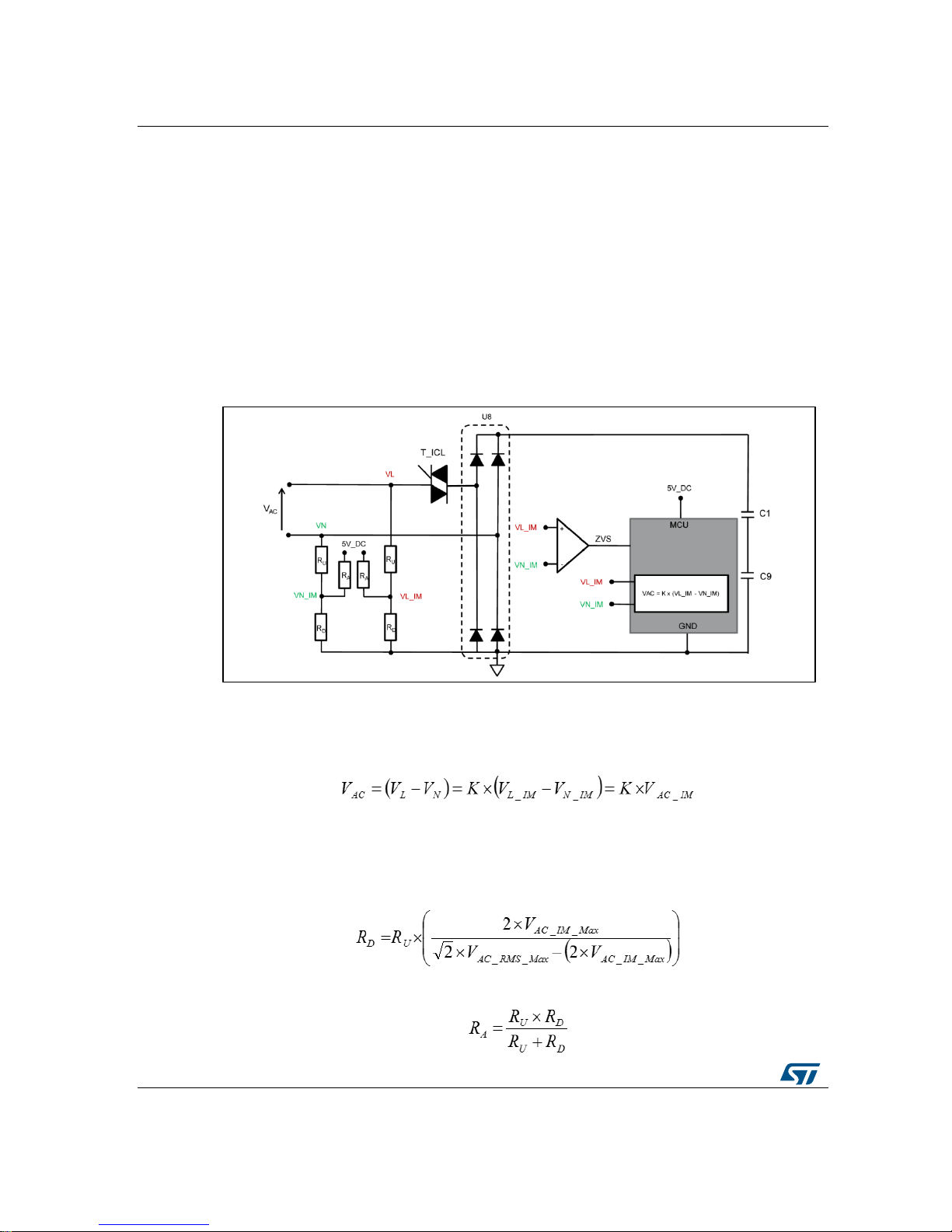
Zero-Voltage and AC line voltage sensor circuits
The AC line voltage (VAC) must be measured to detect the AC line voltage level and to
manage the AC line dips (as described in Section 7: "Mains voltage dips and
interruptions"). As the MCU is connected after the diode bridge, a differential measurement
must be performed to measure the AC line voltage (VAC). The VAC measurement is based
on the line voltage (VL) and the neutral voltage (VN) measurement (VAC = VL - VN). To sense
VL and VN, a resistor divider bridge, with a DC offset (V
OFFSET
) is used (see Figure 18: "AC
line voltage measurement principle"). Thanks to this offset, the images of the VL (V
L_IM
) and
VN (V
N_IM
) remain positive. That means the ICL demo board only requires a single voltage
supply, and not a supplementary negative one to measure VAC.
Figure 18: AC line voltage measurement principle
Given the VL and VN images, the MCU is able to calculate VAC as per the equation below,
where V
AC_IM
is the image of the AC line voltage and K the proportional coefficient between
VAC and V
AC_IM
defined by the resistor divider bridge.
Choosing the RU resistance and given that we set V
L_IM
and V
N_IM
to be centered around
5V_DC / 2, the equation below shows how the user can determine the resistance RD,
where V
AC_RMS_Max
is the maximum RMS AC line voltage which can be applied in the
application and V
AC_IM_Max
is the maximum AC line voltage image voltage that can be
applied in the MCU ADC input specified by the user.
The following equation shows how the end user should choose resistance RA
Page 27

UM2027
AC voltage monitoring and zero-voltage
synchronisation
DocID029048 Rev 1
27/37
The next equation gives the proportional coefficient between VAC and V
AC_IM
.
For example, with RU = 2 MΩ, V
AC_RMS_Max
= 264 V, and V
AC_IM_Max
= 4 V, the following
resistor values and the K parameter are determined. For high accuracy, a 1% resistor
tolerance is recommended.
on the ICL board schematic, the resistor bridges are defined with the following
values:
Zero AC line voltage detection
The TRIAC phase-control needs to be synchronized with the AC line voltage. The zero AC
line voltage crossing detection uses the AC line voltage measurement. Indeed, the zero AC
line voltage occurs when the line voltage (VL) and the neutral voltage (VN) are equal. In this
case, a comparator (U7), connected to the pin 17 of the MCU, compares the V
L_IM
and
V
N_IM
voltage. As soon as V
L_IM
is lower than V
N_IM
the output comparator switches to the
low level, as shown in Figure 18: "AC line voltage measurement principle". This figure
shows that the typical delay of the ZVS signal versus the real VAC zero is 36 µs for a 230
V 50 Hz grid voltage.
Page 28

AC voltage monitoring and zero-voltage
synchronisation
UM2027
28/37
DocID029048 Rev 1
Figure 19: Zero AC line voltage crossing detection
Page 29

UM2027
Triacs and AC switches insulated control
DocID029048 Rev 1
29/37
9 Triacs and AC switches insulated control
The VIPer26LD flyback provides a 5 V DC output voltage. The high terminal of this output
is connected to the line (terminal L1, after the EMI filter); this is why this output is called
VCC_AC, as it is referenced to the AC voltage, not to the DC bus. Moreover, as the upper
level of this output is connected to L1, it allows a negative supply to be implemented. A
negative supply is indeed required to sink the current from the AC switch gates. All the AC
switches on the STEVAL-IHT008V1 boards are so controlled in quadrants 2 and 3. For
more information regarding this, refer to AN3168 or AN4564.
As the MCU is not at the same ground reference as AC switches, optocouplers are needed
to control them. The optocoupler must be chosen to generate enough output current
(optocoupler collector current) to control AC switches according to the input current
(optocoupler LED forward current). In this case, the optocoupler gain, expressed as a
current transfer ratio (CTR), must be chosen according to the equation below, where IGT is
the AC switch gate current and IO_MCU is the output current supplied by the MCU to
control the optocoupler LED.
Given the AC switch gate current (IGT), the gate resistor to limit the AC switch gate current
can be defined according to the following equation, where VCC_AC is the power supply to
provide the gate current to all AC switches and VCE(SAT)_Opto is the transistor collectoremitter of the optocoupler.
In our case, the AC switches (T1 to T5) are controlled by using the IS127 optocoupler (U1,
U2, U3, U4 and U5), see . The CTR of this optocoupler is 1000 and can provide a 20 mA
gate current (which is two times above the 10 mA IGT of the ACS108-8Sx, ACST210 and
Z0109 devices) with R17 = R19 = R20 = R21 = R22 = 91 Ω.
To control the T_ICL AC switch, an optocoupler (U6) associated with a NPN transistor (Q3)
is used as shown in the following figure. Moreover, to improve the NPN transistor immunity,
a RC filter is connected between the base and the emitter of the NPN transistor (R40 = 4.7
kΩ and C10 = 1 nF).
Figure 20: T_ICL AC switch insulated control
The gate resistance (R28) of the T_ICL AC switch is given in the equation below, where
VCC_AC is the power supply to provide the gate current to the AC switch, VCE(SAT)
NPN
is
Page 30

Triacs and AC switches insulated control
UM2027
30/37
DocID029048 Rev 1
the NPN transistor collector-emitter, IGT the TRIAC gate current and VGT is the TRIAC gate
triggering voltage.
The collector resistor (R18) of the NPN transistor is defined in the next equation, with R40
being the NPN transistor resistor filter, VCC_AC the power supply to provide the gate
current to the AC switch, VCE(SAT)
Opto
the transistor collector-emitter of the optocoupler,
IGT the TRIAC gate current, ß
NPN
is the NPN transistor gain and VBE(SAT)
NPN
is the NPN
transistor base-emitter.
Given the optocoupler and the R28 resistor value, the LED resistor R29 of the optocoupler is
defined by the equation below.
in our example, with the IS127 optocoupler and the 2N2222 NPN transistor, the following
resistor values should therefore be chosen.
Page 31

UM2027
EN55014 test results
DocID029048 Rev 1
31/37
10 EN55014 test results
Figure 21: EMI noise test with 1000 W load
Figure 22: EMI noise test without load
Page 32

STEVAL-IHT008V1 silk-screen
UM2027
32/37
DocID029048 Rev 1
11 STEVAL-IHT008V1 silk-screen
Figure 23: STEVAL-IHT008V1 silk-screen (Top side)
Table 5: Bill of material
Reference
Part / Value
C1, C9
1000 µF / 250 V
C2, C4, C5, C8
2.2 nF / 440 VAC
C6, C7
56 nF / 300 V
C10
1 nF / 50 V
C11, C14
1 µF / 25 V
C13, C15, C38
1 nF / 50 V
C16, C17, C18, C19, C20, C21, C24, C26, C27
10 nF / 50 V
C22
100 nF / 50 V
C23
10 µF / 16 V
C25
680 nF / 25 V
C28
220 µF / 16 V
C29
1.5 mF / 16 V
C30
220 µF / 63 V
C31, C37
100 µF / 16 V
C32
10 µF / 450 V
Page 33

UM2027
STEVAL-IHT008V1 silk-screen
DocID029048 Rev 1
33/37
Reference
Part / Value
C33
22 µF / 450 V
C34
2.2 µF / 63 V
C35
680 pF / 50 V
C36
100 nF / 50 V
C39
330 n / 50 V
D1
BZX55C30
D2, D6, D7, D8, D9, D10
LED
D4
BZX55C5V6
D5
BZX55C15
D11, D15, D16
STPS1150
D12
1.5KE300A
D13
1N4007
D14
STTH1l06
D17
D1N4148
D18
bicolor LED
F1
10 A fuse / 250 V
J1, J2, J3, J4, J5, J6, J20
2 way header_ 2.54 mm pitch
J7
4 way header _ 5.08 pitch
J8, J11, J15, J18, J21, J12, J13, J17
2 way plug _ 5.08 pitch
J9, J10
3 way plug _ 5.08 pitch
J14, J19
4 way header _ 2.54 mm pitch
J16
8 way header _ 2.54 pitch
L1
0.012 H / 10 A
L2
1 mH
Q1
BUX87
Q2
STQ1NK80ZR-AP
Q3
2N2222
R1, R2, R3, R4, R5
220 R / 0.125 W
R6
470 R / 0.125 W
R7, R10
250 k / 0.25 W
R8
2.5 k / 5 W
R9, R11, R14, R16
50 k / 0.25 W
R12, R13
250 k / 0.125 W
R15
3.3 k / 0.25 W
R17, R19, R20, R21, R22
91 R / 0.5 W
R18
1.5 k / 0.125 W
R23, R24, R25, R26, R27
270 R / 0.125 W
R28
36 R / 2 W
R29
2.7 k / 0.125 W
R30, R31, R35, R36, R47, R48
1 M / 0.25 W
Page 34

STEVAL-IHT008V1 silk-screen
UM2027
34/37
DocID029048 Rev 1
Reference
Part / Value
R32, R33
300 R / 0.125 W
R34
21.5 k / 0.25 W
R37, R49
16.2 k / 0.25 W
R38, R39
2.7 M / 0.25 W
R40
4.7 k / 0.125 W
R41, R43
16 k / 0,25 W
R42, R50
0 R / 0.125 W
R44
10 kΩ linear potentiometer
R45, R46
100 k / 0.125 W
R51
10 k / 0.125 W
R52, R53
47 R / 1 W
R54
36 k / 0.125 W
R55
10 k / 0.125 W
R56
20 k / 0.125 W
R57
22 k / 0.125 W
R58
150 R / 0.125 W
SIOV1
S07K300 / 300 VAC
SIOV2
S14K300 / 300 VAC
SW1, SW2, SW3, SW4, SW5
micro_switch
SW6
switch_HVDC
SW7
HV_discharge push button
TP1 to TP34
pcb test point terminals
T_ICL
T1635T-8FP
T1
ACST210-8FP
T2, T3
ACS108-8SN
T4, T5
Z0109MUF
T6
myrra74010
U1, U2, U3, U4, U5, U6
IS127
U7
TS861
U8
GBU1007 bridge rectifier /1000 V / 10 A
U9
STM8S103K3
U10, U11
LM2931
U12
viper26LD
Page 35

UM2027
Test points
DocID029048 Rev 1
35/37
12 Test points
The different test points available on the STEVAL-IHT008V1 are given in the table below.
Table 6: Test points
Reference
Designation
Definition
TP1
L1
Line after EMI filter
TP2, TP21,
TP33
VCC_AC
TP3
HVDC
TP4
L
Line before EMI filter
TP5
OUT_ICL
A2 output of T_ICL
TP6
OUT1
A2 output of T1
TP7
OUT2
A2 output of T2
TP8
OUT3
A2 output of T3
TP9
OUT4
A2 output of T4
TP10
OUT5
A2 output of T5
TP11
HVDC/2
TP12
N
Neutral before EMI filter
TP13
N1
Neutral after EMI filter
TP14,
TP24,TP29
GND_DC
TP15
G1
Gate signal of T1
TP16
G2
Gate signal of T2
TP17
G3
Gate signal of T3
TP18
G4
Gate signal of T4
TP19
G5
Gate signal of T5
TP20
G_ICL
Gate signal of T_ICL
TP22
GND_AC
TP23
15V_DC
TP25
VCC_INS
TP26
Drain_viper
TP27
GND_INS
TP28
5V_DC
TP30
ZVS
TP31
VL1_MEAS
MCU input for line
measurement
TP32
VN1_MEAS
MCU input for neutral
measurement
TP34
MAX INRUSH CURRENT ORDER
Page 36

Revision history
UM2027
36/37
DocID029048 Rev 1
13 Revision history
Table 7: Document revision history
Date
Revision
Changes
09-Mar-2016
1
Initial release.
Page 37

UM2027
DocID029048 Rev 1
37/37
IMPORTANT NOTICE – PLEASE READ CAREFULLY
STMicroelectronics NV and its subsidiaries (“ST”) reserve the right to make changes, corrections, enhancements, modifications , and
improvements to ST products and/or to this document at any time without notice. Purchasers should obtain the latest relevant information on ST
products before placing orders. ST products are sold pursuant to ST’s terms and conditions of sale in place at the time of order
acknowledgement.
Purchasers are solely responsible for the choice, selection, and use of ST products and ST assumes no liability for application assistance or the
design of Purchasers’ products.
No license, express or implied, to any intellectual property right is granted by ST herein.
Resale of ST products with provisions different from the information set forth herein shall void any warranty granted by ST for such product.
ST and the ST logo are trademarks of ST. All other product or service names are the property of their respective owners.
Information in this document supersedes and replaces information previously supplied in any prior versions of this document.
© 2016 STMicroelectronics – All rights reserved
 Loading...