

Page 1
UM2792
User manual
Getting started with the STEVAL-DPSTPFC1 3.6 kW PFC totem pole with inrush
current limiter reference design
Introduction
The STEVAL-DPSTPFC1 3.6 kW bridgeless totem pole boost circuit achieves a digital power factor correction (PFC) with inrush
current limiter (ICL). It helps you to design an innovative topology with the latest ST power kit devices: silicon carbide MOSFETs
(SCTW35N65G2V), thyristor SCRs (TN3050H-12WY), isolated FET drivers (STGAP2S) and a 32-bit MCU (STM32F334).
This reference design also opens the path to a compact converter running at 72 kHz offering a high peak efficiency, low THD
distortion (97.5 % with 3.7 % THD) and reduced bill of materials.
It achieves a robust circuit that meets EMC standards up to 4 kV delivering high switching lifetime with reduced EMI emissions.
Thyristor SCRs used as AC line polarity switches allow achieving an active current limitation at power up or line drop recovery:
the PFC efficiency is optimal and no EMI bouncing effect occurs.
The reference design includes a power board with a bridgeless totem pole boost (with an inrush limiter circuit, switch drivers and
an auxiliary power supply), a control board with its MCU, a PFC/ICL control firmware and an adapter board for software debug.
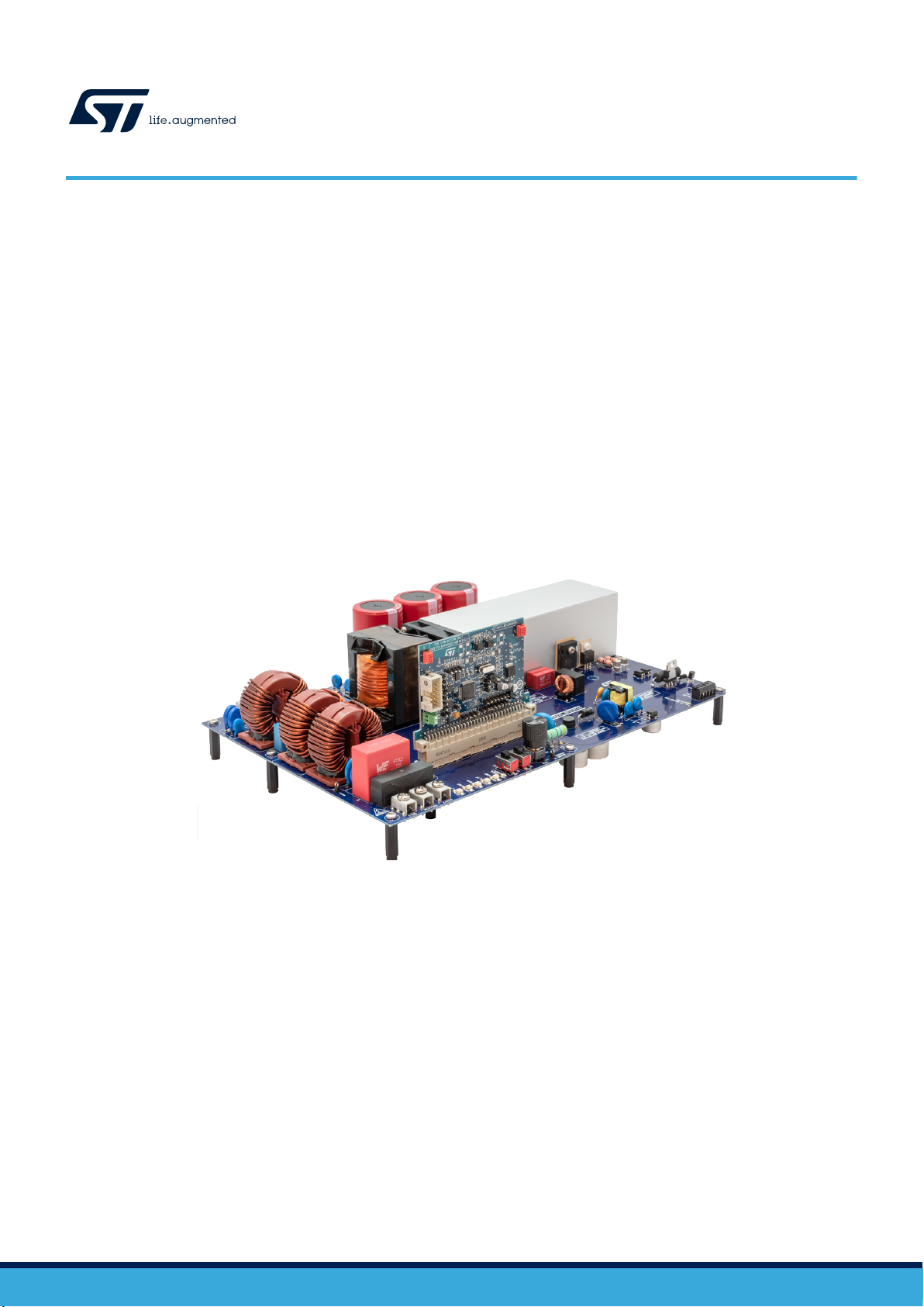
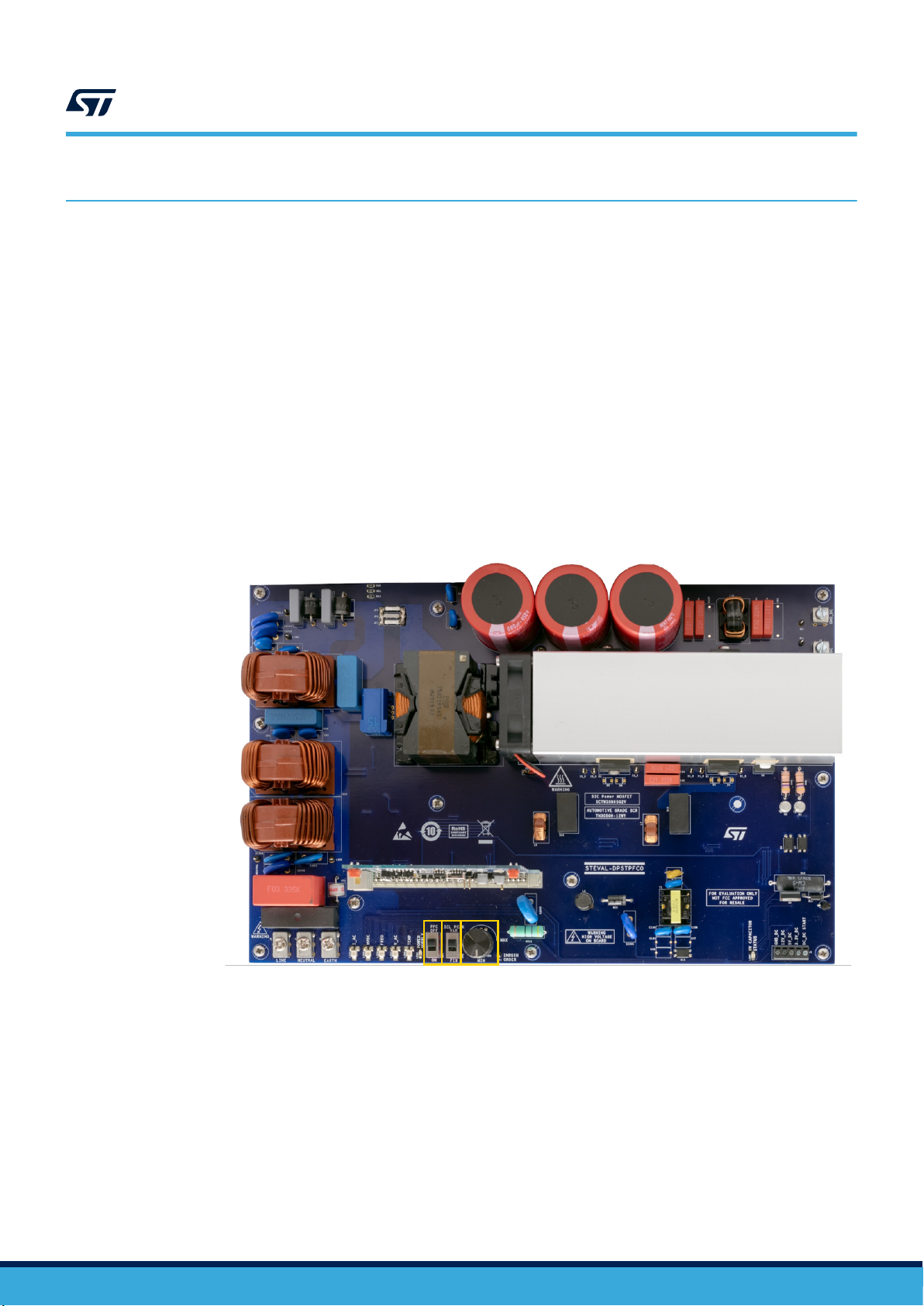
Figure 1. STEVAL-DPSTPFC1 totem pole
UM2792 - Rev 1 - January 2021
For further information contact your local STMicroelectronics sales office.
www.st.com
Page 2
UM2792
Getting started
1 Getting started
1.1 Safety instructions
Attention: The STEVAL-DPSTPFC1 evaluation board is designed for demonstration purposes only and is not intended for
domestic or industrial installations.
Danger:
The high voltage levels used to operate the STEVAL-DPSTPFC1 evaluation board could provoke
a serious electrical shock. This evaluation board has to be used in a suitable laboratory by
qualified personnel only, familiar with the installation, use, and maintenance of power electrical
systems.
The STEVAL-DPSTPFC1 radiated field levels could exceed the general public exposure limit if
positioned at less than 60 cm.
During operation, do not touch the board as some of its components could reach a very high
temperature.
1.2
Overview
The STEVAL-DPSTPFC1 is a 3.6 kW PFC totem pole controlled by an STM32 MCU. It has been designed to
offer high performances in terms of efficiency, THD, power factor and reliability by controlling the inrush current at
board startup.
The totem pole board is composed of three different boards:
• an AC-DC power board
• a digital control board based on the STM32F334 microcontroller used to control the PFC stage
• an adapter board to debug the MCU firmware
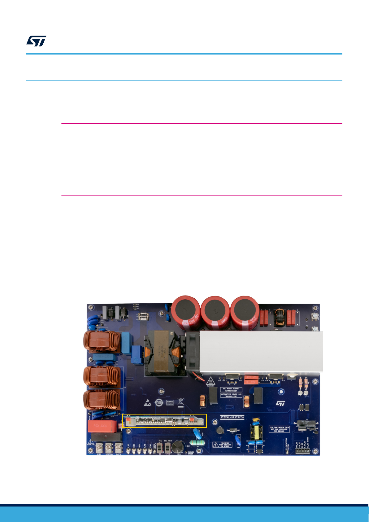
Figure 2. STEVAL-DPSTPFC1 AC-DC power board and PFC control board (highlighted in yellow)
UM2792 - Rev 1
page 2/101
Page 3
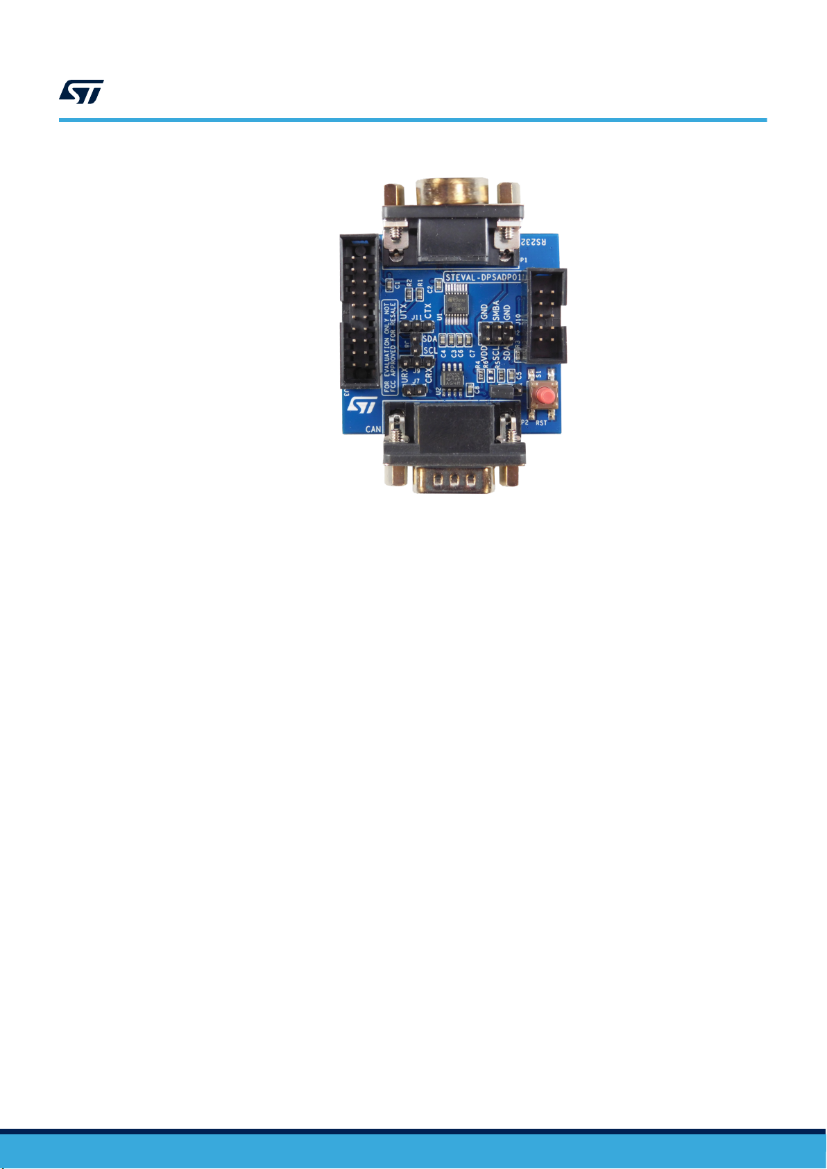
Figure 3. STEVAL-DPSTPFC1 adapter board
UM2792
Main components
1.3
The STEVAL-DPSTPFC1 offers:
• inrush current limitation without inrush current resistor or NTC and relay
• very high efficiency AC-DC conversion
• DC power stage disconnection from the AC line grid thanks to SCRs
Main components
The STEVAL-DPSTPFC1 main components are:
• TN3050H-12WY inrush current limiter SCRs
• SCTW35N65G2V SiC MOSFETs
• STM32F334 MCU
• VIPER26LD flyback IC
UM2792 - Rev 1
page 3/101
Page 4
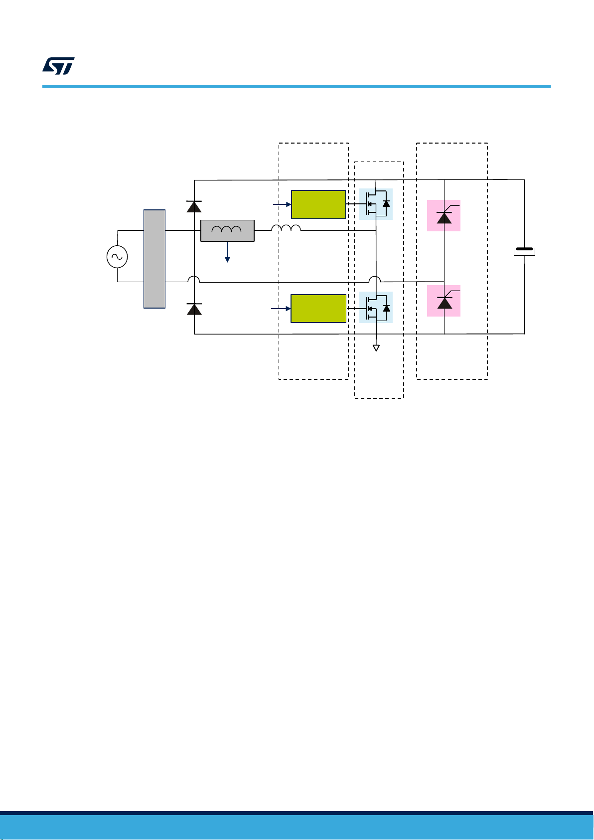
Figure 4. STEVAL-DPSTPFC1 main component diagram
Insulated
SCR
1
1
TN3050H-12WY
SCTW35N65G2V
STGAP2S
V
Driver
Current sensor
AC
S
AC
insulated
I
2
2
HVDC
Driver
Input filter
S
SCR
UM2792
Main components
UM2792 - Rev 1
page 4/101
Page 5
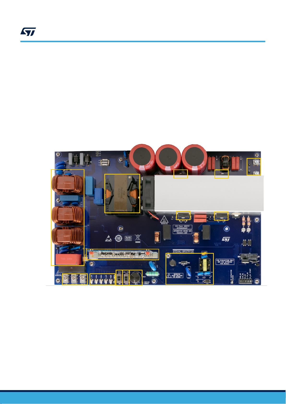
Figure 5. STEVAL-DPSTPFC1 components - overview
1
2
3
4
5
6
7
8
9
10
11
12
13
14
1. Common mode filter + MOV
2. Boost inductor
3. SCR
4. SCR
5. DC load connectors
6. SiC MOSFET
7. SiC MOSFET
8. DC power supply
9. MCU daughter board
10. Potentiometer to control peak inrush current
11. ICL strategy control switch
12. ICL startup switch
13. PFC LEDs status
14. AC line connectors
UM2792
Main components
UM2792 - Rev 1
page 5/101
Page 6
1.4 Totem pole PFC specifications
Table 1. PFC electrical specifications
Description Symbol Min. Typ. Max. Unit Comments
Input
AC line voltage
AC line frequency HZ 45 65
AC line current
Maximum input power PIN MAX
Output
Output voltage regulated HVDC 400 420
HVDC ripple Vripple (PK-PK) 15 V
Maximum output DC current
Control
Switching frequency Fs 72 kHz
Operating temperature
Maximum ambient temperature
V
AC
IAC MAX
IDC Max
T
AMB
MAX
85 264
16
3.6 kW
1.8 kW
9 A
4 A
45 °C
UM2792
Totem pole PFC specifications
V
RMS
A
RMS
VAC = 230 V
IAC MAX = 16 A
VAC = 110 V
IAC MAX = 16 A
V
DC
P
OUT
VAC = 230 V
IAC MAX = 16 A
P
OUT
VAC = 230 V
IAC MAX = 16 A
P
OUT
VAC = 110 V
IAC = 16 A
RMS
RMS
RMS
RMS
= 3.6 kW
RMS
RMS
= 3.6 kW
RMS
RMS
= 1.7 kW
RMS
RMS
UM2792 - Rev 1
Table 2. PFC temperature specifications
Description
Thermal components
Inductor T_Choke 120 °C T
Sic MOSFETs TC_MOS 80 °C
SCRs TC_SCR 65 °C
Symbol Min. Typ. Max. Unit Comments
= 30°C
AMB
FAN ON
P
= 3.6 kW
OUT
VAC = 230 V
RMS
IAC MAX = 16 A
RMS
page 6/101
Page 7
Totem pole PFC specifications
Table 3. PFC protection specifications
Description Symbol Min. Typ. Max. Unit Comments
HVDC overvoltage protection 450 VDC
IAC peak overcurrent protection
24 A
Table 4. Passive component specifications
Description Symbol Min. Typ. Max. Unit Comments
Primary EMI filter inductor
Output capacitor
L_FILT
L3 / L4 / L14
C_HVDC
C76/C77/C78
3 x 1.6 mH
3 x 680 µF
Table 5. PFC efficiency specifications
Description Symbol Min. Typ. Max. Unit Comments
Power factor
230 V
PF 0.9903 N.A.
PF 0.9956 N.A.
PF 0.9965 N.A.
PF 0.9932 N.A.
PF 0.9982 N.A.
PF 0.9981 N.A.
Distortion
THD 6.9 %
THD 3.7 %
THD 3.5 %
THD 9.7 %
THD 4.6 %
THD 4.2 %
RMS
IAC = 4.5 A
230 V
RMS
IAC = 8.8 A
230 V
RMS
IAC = 15.5 A
110 V
RMS
IAC = 3.8 A
110 V
RMS
IAC = 9.5 A
110 V
RMS
IAC = 15.5 A
230 V
RMS
IAC = 4.5 A
230 V
RMS
IAC = 8.8 A
230 V
RMS
IAC = 15.5 A
110 V
RMS
IAC = 3.8 A
110 V
RMS
IAC = 9.5 A
110 V
RMS
IAC = 15.5 A
UM2792
/50 Hz
RMS
/50 Hz
RMS
/50 Hz
RMS
/60 Hz
RMS
/50 Hz
RMS
/60 Hz
RMS
/50 Hz
RMS
/50 Hz
RMS
/50 Hz
RMS
/60 Hz
RMS
/50 Hz
RMS
/60 Hz
RMS
UM2792 - Rev 1
page 7/101
Page 8

Description Symbol Min. Typ. Max. Unit Comments
Efficiency
230 V
η 96.8 %
η 97.5 %
η 97.2 %
η 92.4 %
η 94.8 %
η 94.6 %
RMS
IAC = 4.5 A
230 V
RMS
IAC = 8.8 A
230 V
RMS
IAC = 15.5 A
110 V
RMS
IAC = 3.8 A
110 V
RMS
IAC = 9.5 A
110 V
RMS
IAC = 15.5 A
UM2792
Status LEDs
/50 Hz
RMS
/50 Hz
RMS
/50 Hz
RMS
/60 Hz
RMS
/50 Hz
RMS
/60 Hz
RMS
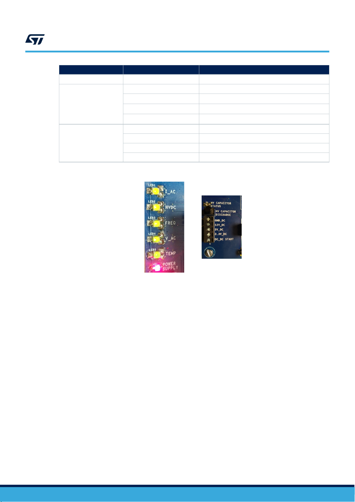
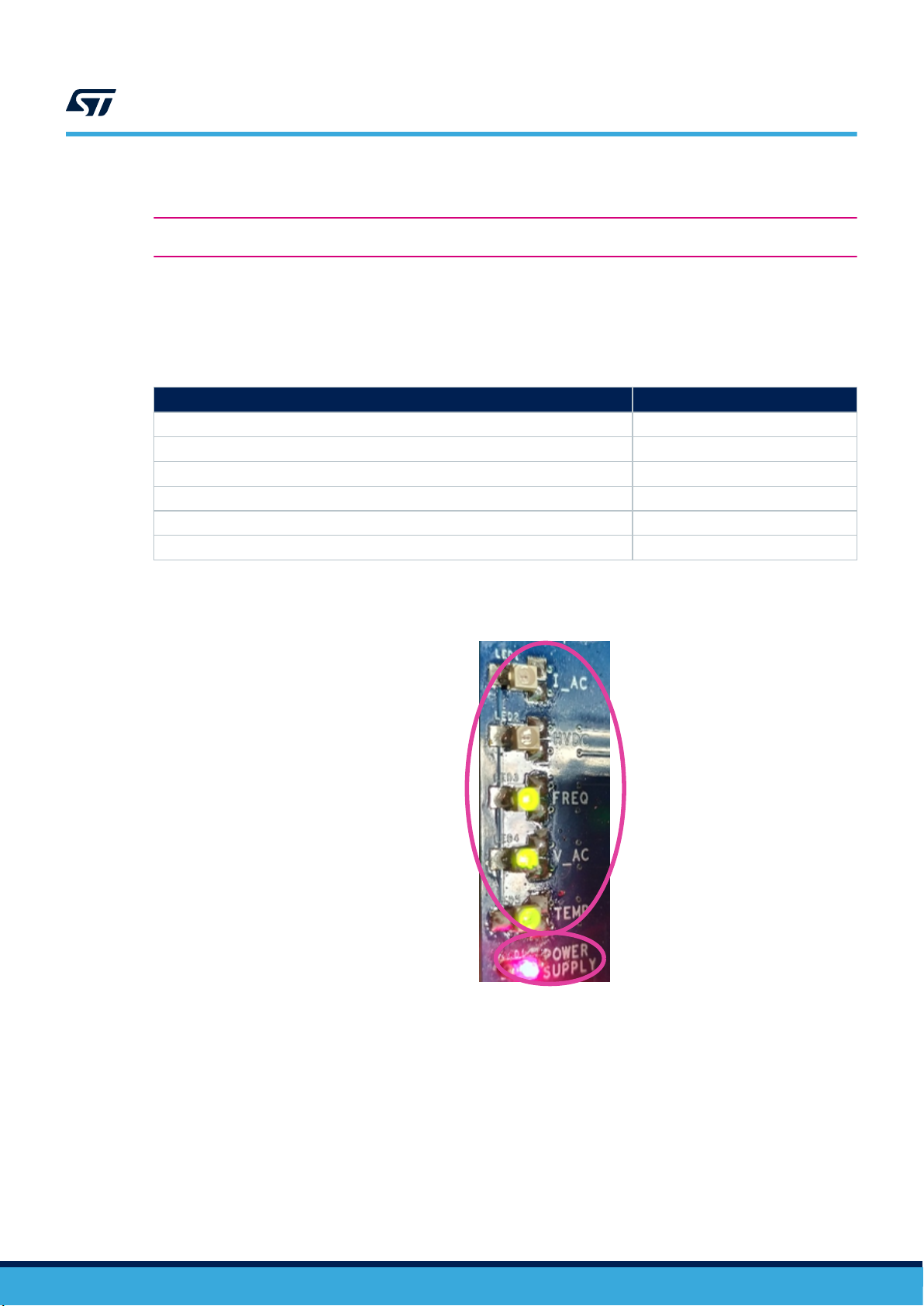
1.5 Status LEDs
The following board LEDs define the PFC status:
• HV CAPACITOR DISCHARGE - LED7: lights up in red when the HVDC output voltage is higher than 30 V
(voltage between HVDC and GND_DC terminals)
Danger:
While LED7 is red, the DC output capacitor is not discharged and could provoke a serious
electrical shock
• POWER_SUPPLY - LED6: lights up in red when the PFC totem pole board is powered
• PFC STATUS LEDs (LED 1/2/3/4/5): at board startup, all these LEDs are alternatively lit in red, then orange,
green and then OFF. This indicates the microcontroller has finalized the initialization procedure (right mains
connection, line frequency measurement, power supply available, etc.) and the board is ready to be used.
From this moment, the DC output capacitor can be charged when the HVDC switch (SW1) is in the ON
position.
LEDs definition LEDs state Comments
IAC (LED1)
HVDC (LED2)
FREQ (LED3)
Table 6. Status LEDs
OFF PFC board not supplied
GREEN
RED IAC_Peak > 25 A
OFF PFC board not supplied
GREEN
GREEN FLASHING DC output capacitor in charge
ORANGE
RED
OFF PFC board not supplied
GREEN 45 Hz < AC Line frequency < 65 Hz
ORANGE AC Line frequency < 45 Hz
IAC < 16 A
RMS
HVDC = 400 V
HVDC < 380 V
HVDC > 450 V
DC
DC
DC
DC
UM2792 - Rev 1
page 8/101
Page 9
LEDs definition LEDs state Comments
FREQ (LED3)
RED AC Line frequency > 65 Hz
OFF PFC board not supplied
VAC (LED4)
GREEN
ORANGE
RED
85 V
< VAC < 264 V
RMS
VAC < 85 V
VAC > 264 V
OFF PFC board not supplied
TEMP (LED5)
GREEN Heat sink temperature < 120 °C
ORANGE N.A.
RED Heat sink temperature > 120°C
Figure 6. PFC status LEDs overview
UM2792
Status LEDs
RMS
RMS
RMS
UM2792 - Rev 1
page 9/101
Page 10
2 Board connection and startup
1
2
3
2.1 Mechanical switches and potentiometer configuration
Step 1. Push the FC switch (SW1) on OFF position
Step 2. To control the inrush current by SCRs with a constant progressive phase control, push the ICL_PEAK
switch (SW2) on VAR position. The constant progressive phase control value is defined by the max.
inrush current potentiometer (R30)
Step 3. To control the inrush current by SCRs with a variable progressive phase control, push the ICL_PEAK
switch on FIX position.
Step 4. The max. inrush current potentiometer (R30) value is read only by the MCU if the ICL_PEAK switch
is set to VAR position. Max. inrush current potentiometer is used to define the constant progressive
phase control value. The DC capacitor charge speed can be increased if the allowed peak current is
increased. For this purpose, the max. inrush current potentiometer has to be turned clockwise.
Figure 7. STEVAL-DPSTPFC1 switches and potentiometer
1. PFC switch (SW1)
2. ICL_PEAK switch (SW2)
3. Max. inrush current potentiometer (R30)
UM2792
Board connection and startup
UM2792 - Rev 1
page 10/101
Page 11
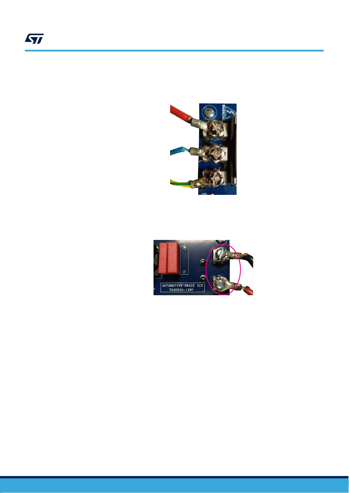
2.2 AC line wires connection
Step 1. Connect the line (L), neutral (N) and earth (PE) wires with J3, J6 and J7 headers, respectively, to an
unpowered mains plug.
UM2792
AC line wires connection
Figure 8. AC line wire connection overview
2.3 Output DC load connection
Step 1. Connect the DC load between the HVDC and GND_DC connectors.
Figure 9. STEVAL-DPSTPFC1 output HVDC connection
If an electronic DC load is used:
– connect the positive input of the electronic DC load to HVDC connector
– connect the negative input of the electronic DC load to GND_DC connector
UM2792 - Rev 1
page 11/101
Page 12
2.4 PFC board power on
Step 1. Put the AC line voltage ON.
Danger: Do not touch components under the AC line voltage.
The power supply LED6 lights up in red to signal the PFC totem pole board is powered. The PFC
status LEDs (LED1/2/3/4/5) blinking sequence is red, orange, green. At board startup, parameters like
VAC, IAC, temperature and current sensor are checked. After board initialization, the PFC status LEDs
light up as per the table and figure below.
POWER SUPPLY - LED6 Red light
UM2792
PFC board power on
Table 7. STEVAL-DPSTPFC1 LEDs
Definition State
I_AC - LED1 OFF
HVDAC - LED2 OFF
FREQ - LED3 Green light
V_AC - LED4 Green light
TEMP - LED5 Green light
1. PFC status LEDs (LED1/2/3/4/5)
2. Power supply (LED6)
Figure 10. LED status overview
UM2792 - Rev 1
page 12/101
Page 13
2.5 PFC startup
Step 1. Slide the PFC switch (SW1) to ON to start up the PFC totem pole board (see Figure 7)
The PFC status LEDs must light up as per the following table and Figure 6.
2.6 PFC board turn off
Step 1. Slide the PFC switch (SW1) to OFF position to start up the PFC totem pole board (see Figure 7)
The PFC status LEDs must light up as per the following table and Figure 6. PFC status LEDs overview.
UM2792
PFC startup
Table 8. PFC LED status
Definition Status
I_AC - LED1 Green light
HVDAC - LED2 Green light
FREQ - LED3 Green light
V_AC - LED4 Green light
TEMP - LED5 Green light
POWER SUPPLY - LED6 Red light
HV_CAPACITOR STATUS Red light
Table 9. PFC LED status
Definition Status
I_AC - LED1 OFF
HVDAC - LED2 OFF
FREQ - LED3 Green light
V_AC - LED4 Green light
TEMP - LED5 Green light
POWER SUPPLY - LED6 Red light
HV_CAPACITOR STATUS - LED7 OFF
Note: HV_CAPACITOR STATUS (LED7) switches off after an interval of time that depends on the DC load impedance
(around 3 minutes if no DC load is connected to the HVDC output).
Danger:
When HV_CAPACITOR STATUS (LED7) lights up in red, the DC output capacitor is not
discharged and could provoke a serious electrical shock. This LED remains switched on as long
as the HVDC voltage remains above 30 V.
UM2792 - Rev 1
page 13/101
Page 14
3 DC bus capacitor discharge
R67
HVDC
STQ1NK80ZR-AP
R103
STN4NF03L
D11
D8
Q4
165k
R66
MMSZ5256BT1G
Q5
STN4NF03L
MMSZ5V6T3G
R65
High voltage
visualization
165k
1k
R105
Q7
3.3k
R106
5V_DC
HV_DISCHARGE
R64
R68
GND_DC
165k
R104
Q6
MMSZ5245BT1G
D10
10k
33k 5W
R63
165k
P6KE440A
BUL216
165k
DZ1
165k
HV capacitor discharge
A circuit has been implemented to accelerate the output DC capacitors (C76, C77 and C78) discharge through
R63 resistor. This circuit is turned on every time the PFC board is in OFF state. The full discharge time takes
around 3 minutes when no DC load is connected. LED7 (HV CAPACITOR DISCHARGE) is lit up as long as the
HVDC voltage remains above 30 V.
Figure 11. DC bus capacitor discharge circuit
UM2792
DC bus capacitor discharge
UM2792 - Rev 1
page 14/101
Page 15
4 Additional external components
The STEVAL-DPSTPFC1 board allows adding some external components to the front-end circuit.
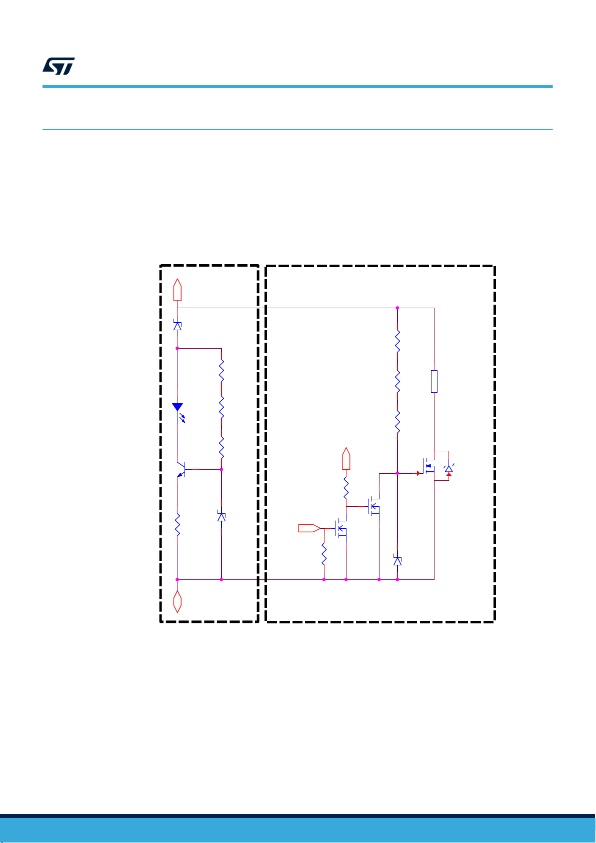
4.1 DC-DC circuit connection
A DC-DC converter can be connected to the HVDC bus via HVDC (J3) and GND_DC (J8) connectors. To allow
the correct operation of the STEVAL-DPSTPFC1 front-end circuit, the DC-DC converter has to be activated after
the PFC_START signal has been set to high level state. The PFC_START signal indicates the PFC is operational
and the HVDC output voltage is 400 VDC. This signal refers to GND_DC terminal and is available from the J1
header.
Figure 12. DC-DC converter activation (DC_DC_Start signal) when PFC totem pole is operational
VAC = AC line voltage
IAC = AC line current
HVDC = PFC output voltage
UM2792
Additional external components
4.2 Motor inverter connection
An inverter can be added behind the HVDC bus output. A 12 V positive output, referred to the DC Bus Ground
(GND_DC), is available on header J1 to supply an IPM module, if needed.
4.3 Control through an external microcontroller
Instead of using the embedded MCU daughter board, the STEVAL-DPSTPFC1 can be controlled through an
external MCU daughter board to directly check the compliance of its firmware with this board circuit. For
pin numbers and names of the daughter board connectors, refer to the external connectors section shown in
Figure 87. STEVAL-DPSTPFC0 circuit schematic (1 of 4).
UM2792 - Rev 1
page 15/101
Page 16
5 Totem pole PFC control
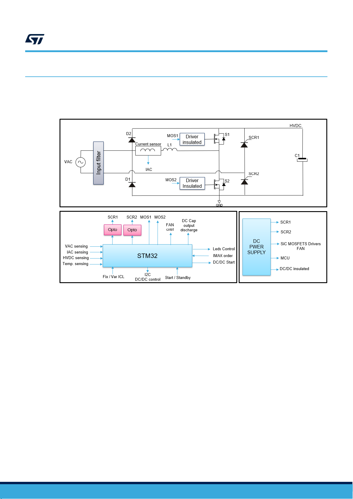
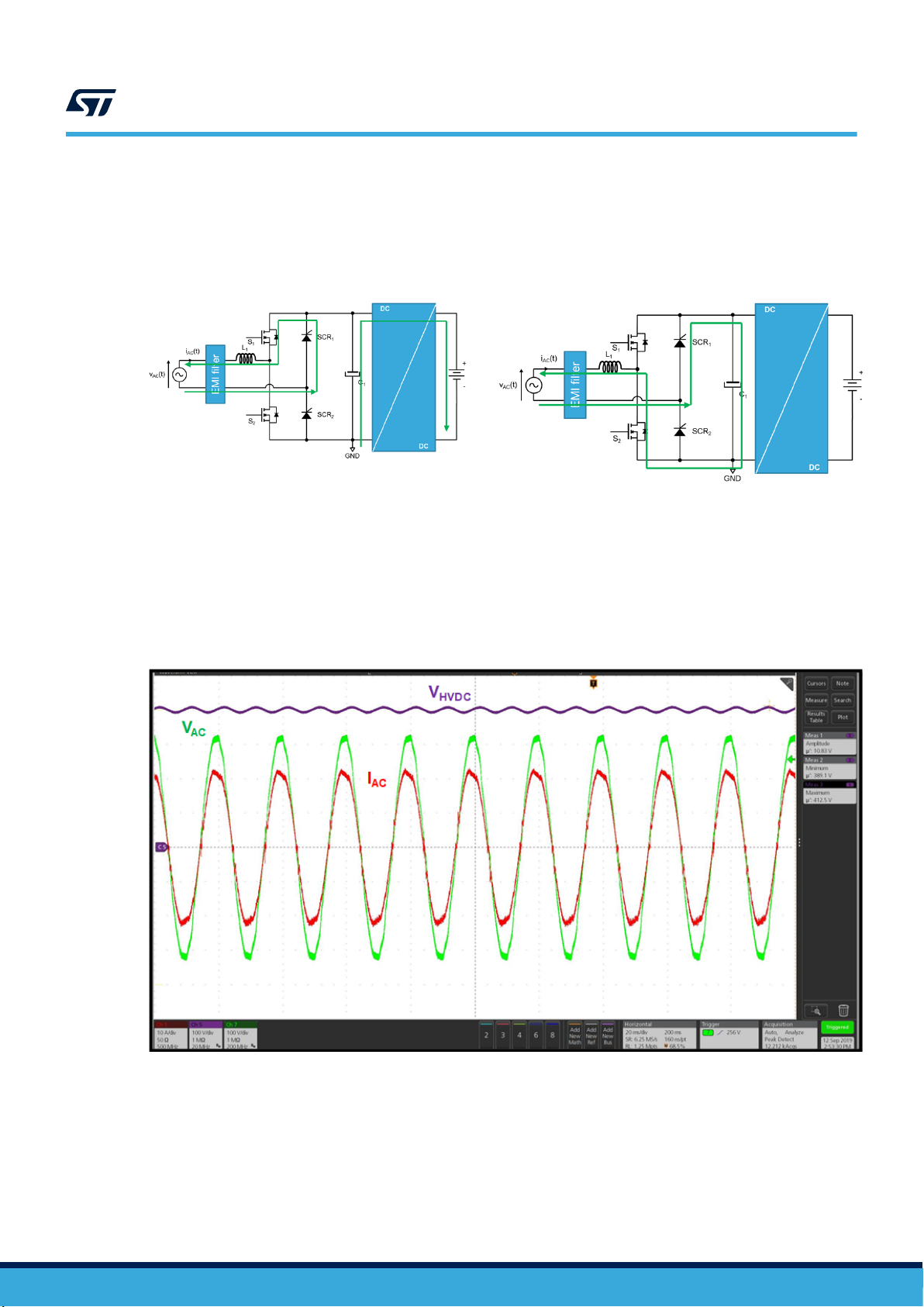
5.1 Bridgeless PFC totem pole overview
Figure 13. Bridgeless PFC totem pole synoptic
UM2792
Totem pole PFC control
The figure above highlights the main components:
• SCRs (SCR1 and SCR2) in the bridgeless PFC totem pole to:
– control inrush current at board startup
– disconnect the DC link bus (HVDC) from the AC line voltage
• SiC MOSFETs (S1 and S2) to shape the input AC line current
• STGAP2S drivers to control SiC MOSFETs
• an STM32 MCU which mainly drives SCRs and SiC MOSFETs
• a flyback power converter providing:
– 5V_SCR1: 5 VDC insulated output. This supply is used to control SCR1
– 5V_SCR2: 5 VDC insulated output. This supply is used to control SCR2
– 12V_DC: 12 VDC insulated regulated output referenced to the DC bus ground (GND_DC). This supply
is used to supply the insulated DC-DC converter (needed by SiC MOSFETs) and the fan. From this 12
VDC:
◦ a 5V_DC is created to supply current sensor
◦ a 3V3_DC is created to supply the PFC board control and all the control circuits
UM2792 - Rev 1
page 16/101
Page 17
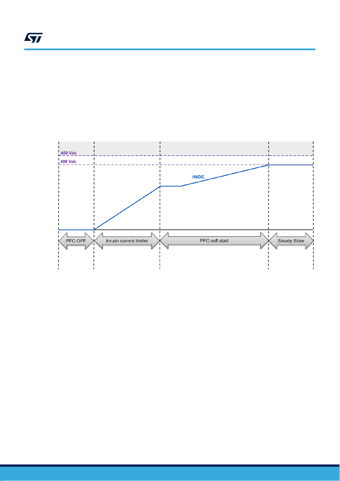
5.2 Soft start
To ensure a smooth PFC startup, a soft start procedure has been implemented in the STM32 MCU:
• to reduce the inrush current at board startup, SCRs are controlled by a progressive phase control and the
output DC capacitor can smoothly increase up to the AC line peak voltage
• to reduce the inrush current when the PFC output voltage (HVDC) switches from the peak AC line voltage to
regulated 400 V
• once the PFC output voltage reference is reached, the PFC output DC voltage (HVDC) is regulated
according to output and input conditions
UM2792
Soft start
DC
Figure 14. PFC soft start principle
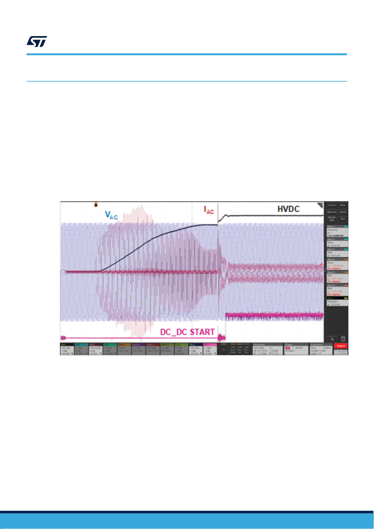
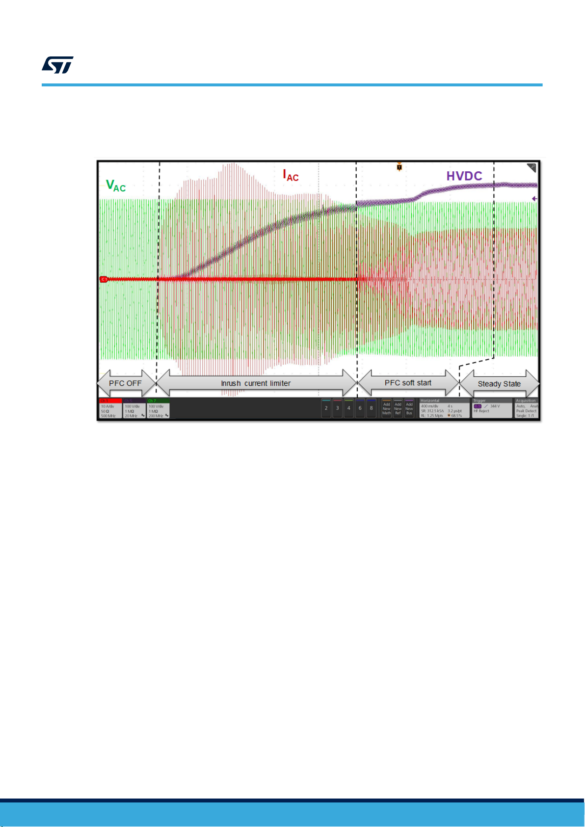
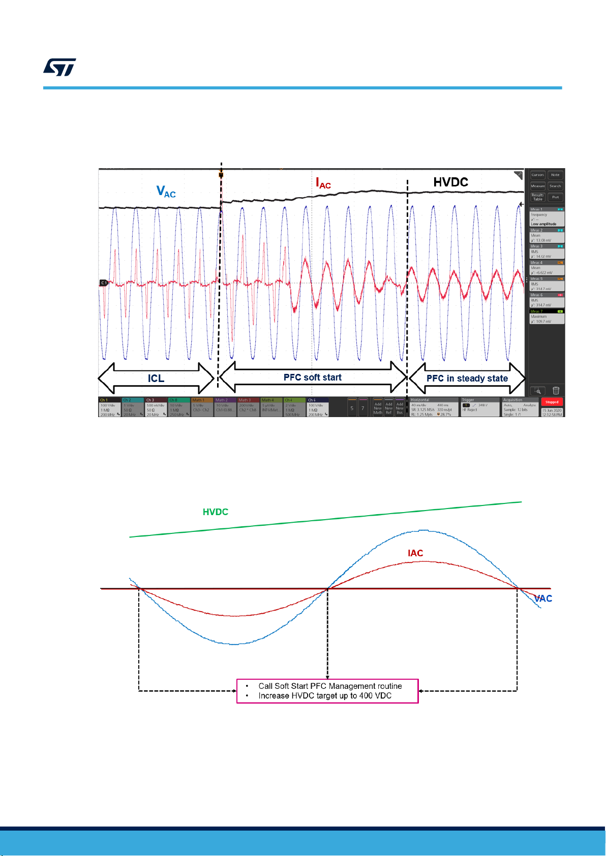
The following figure shows an example of the described progressive PFC soft start. Tests have been performed at
board startup with the board connected to a 230 V 50 Hz grid (VAC) with a 3.3 kW DC load.
UM2792 - Rev 1
page 17/101
Page 18
VAC = AC line voltage
IAC = AC line current
HVDC = PFC output voltage
UM2792
Inrush current control
Figure 15. PFC soft start procedure
5.3 Inrush current control
5.3.1 IEC 61000-3-3 standard
The IEC 61000-3-3 standard gives the limitation of voltage changes and fluctuations for equipment with rated
RMS current lower than 16 A when connected to a public low voltage grid.
If a too high current is sunk from the grid, the equipment causes these voltage fluctuations and voltage drop
occurs due to the line impedance.
The mains voltage fluctuation causes undesired brightness variation of lamps and displays (flicker phenomenon).
For this reason, you should keep the inrush current sunk by your equipment lower than the specified limits.
5.3.2 Inrush current controlled by NTC resistor
Usually, the PFC totem pole uses diodes (D1/D2) or a standard MOSFET (S3/S4) operating at low frequency.
However, MOSFETs or diodes need a resistor or an NTC (RLim) to control the inrush current at board startup.
The resistor has then to be bypassed by a relay (RL2) to limit the power losses during steady state operation. To
disconnect the DC bus in standby mode, a second relay (RL1) is required. In steady state operation, this solution
increases global power losses due to the relay contact resistor as well as the PFC converter cost.
Note: The contact resistor value increases according to the number of operating cycles and, therefore, decreases PFC
efficiency.
UM2792 - Rev 1
page 18/101
Page 19
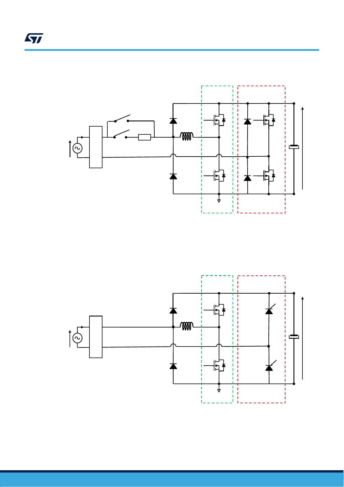
Figure 16. PFC totem pole topology with NTC resistor
Low frequency
Diodes or MSOFETs
1
High frequency
4
D
1
D
BP2
GND
S
1
V
AC
AC
S
SiC MOSFETs
2
RLim
RL
EMI FILTER
RL
1
D
3
BP1
2
D
HVDC
S
S
I
C
L
2
SCR
EMI FILTER
S
Low frequency
D
SCRs
BP2
C
GND
SiC MOSFETs
1
V
AC
AC
1
S
BP1
D
1
SCR
L
HVDC
2
I
High frequency
2
UM2792
Inrush current control
5.3.3 Inrush current controlled by SCRs
With the totem pole PFC the capacitor can be smoothly charged with a progressive phase control and avoid the
use of an NTC or a resistor thanks to SCRs.
Figure 17. PFC totem pole topology with SCRs
UM2792 - Rev 1
page 19/101
Page 20
T_OFF_2
TT
T
T_OFF_Max
∆t
5x∆t
2x∆t
3x∆t
TT
T
HVDC
SCR1
T_OFF_Min
T
SCR2
AC
T_OFF_3
T_OFF_1
4x∆t
V
UM2792
Inrush current control
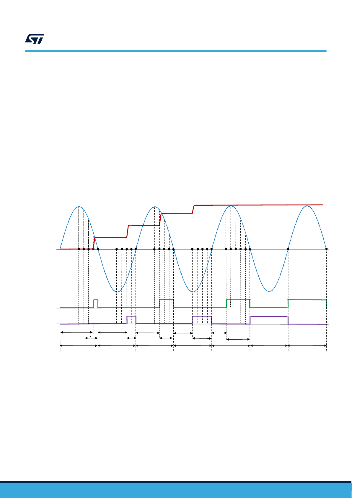
As long as SCRs are not triggered, the bridge does not conduct current and the DC bus capacitor is not charged.
To start charging the DC capacitor, SCR1 and SCR2 have to be turned on according to the AC line voltage
polarity (SCR1 is turned on when the AC line polarity is negative and SCR2 is turned on when the AC line polarity
is positive). To reduce the inrush current, SCRs are alternatively triggered at the end of the half line voltage cycle,
just few hundreds of microseconds before the line zero voltage. This allows the output capacitor to be charged to
a low level (around 10 to 30 V) and not directly to the peak line voltage. The current driven from the line is then
much lower than in case of a direct full charge of the DC capacitor.
This soft start solution can work only when an inductor is present on the line side as the rate of current increase
has also to be limited to prevent SCRs damage. The inductor is already present for most applications where
the EMI filter usually embeds a common mode choke which has a differential mode parasitic inductor due to the
copper turns of the windings.
To control the inrush current at PFC board startup with SCRs, two solutions have been implemented in the MCU
firmware: fixed SCRs on delay and variable SCRs on delay
Fixed SCRs on delay
To allow a complete charge of this capacitor to the peak line voltage, SCRs have to be triggered on the
subsequent half cycle with a shorter turn on delay than the one used to start charging. With VAC, the AC line
voltage and HVDC represent the PFC output voltage.
Figure 18. HV capacitor charges controlled by SCRs
UM2792 - Rev 1
By reducing SCRs turn-on delay by few tens or hundreds of microseconds from half-cycle to half-cycle, the output
capacitor is progressively charged while the line current is kept low. The step of SCRs turn-on delay reduction is
constant from one half-cycle to the following one.
The step of SCRs turn-on delay is defined by reading the MAX_INRUSH CURRENT potentiometer value
on the PFC totem pole board (see Eq. (1)). In the firmware, the step of SCRs turn-on delay is called
Delta_Phase_Angle_μs. Step_Phase_Control_Min_μs is the allowed minimum step of SCRs turn-on
delay (30 μs) and the Delta_Phase_Control_Max_μs parameter is the allowed maximum step of SCRs
turn-on delay (200 μs).
Delta_Control_Max_μs × ADC_Value
12
2
Delta_Pℎase_Angle_μs =
+ Step_Pℎase_Control_Min_μs
(1)
page 20/101
Page 21
UM2792
Inrush current control
When the SCRs turn-on delay is lower than 3 ms, the SCRs gate pulse is directly set to a continuous DC pulse
according to the AC line polarity (SCR1 is set to continuous DC pulse when the AC line polarity is negative and
SCR2 is set to continuous DC pulse when the AC line polarity is positive). Below approximately a 5 ms or 4.2
ms delay (respectively for 50 and 60 Hz line frequency), the output DC capacitor is fully charged. So it is not
necessary to ensure a soft start for turn-on delays much lower than a fourth cycle. In the firmware, the SCRs
turn-on delay to switch SCRs to a continuous DC pulse is called Phase_Control_ON_Max_μs.
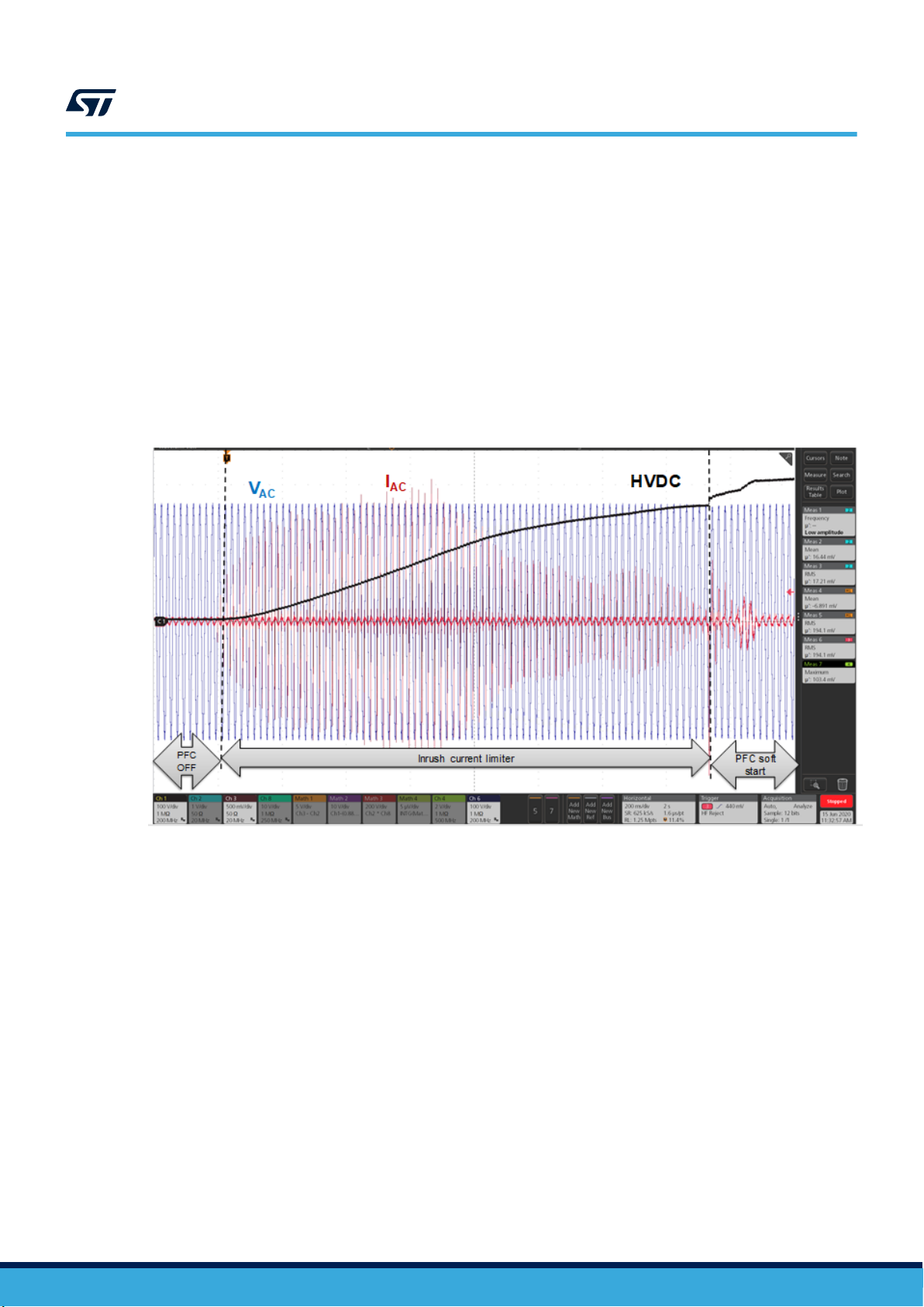
The following figure shows an example of progressive DC capacitor charge. The test has been performed at
startup when the STEVAL-DPSTPFC1 board is connected to a 230 V 50 Hz grid without an output DC load, while
the output DC capacitor is fully uncharged (i.e., its initial voltage is null). In these conditions, the maximum inrush
peak current is around 30 A and the output capacitor is charged in 1.5 s.
Figure 19. Inrush current control at board startup (with fixed SCRs on delay)
HVDC=PFC output voltage
IAC = AC line current
VAC = AC line voltage
UM2792 - Rev 1
Variable SCRs on delay
The peak current during the output capacitor charge is not constant. Only the reduction step of the SCRs turn-on
delay is constant. According to the time of the SCR turn-on, peak current can slightly vary from one period of the
AC line voltage to another. In this case, a second solution has been implemented in the firmware: by reducing
the SCRs turn-on delay defined in a look-up table, half-cycle to half-cycle, the output capacitor is progressively
charged while the line current is kept low with a constant value.
The look up table is defined according to the AC line voltage model (equivalent inductance and resistance), the
input common filter, the output DC bulk capacitor and the dynamic resistance of the SCRs and MOSFETs.
page 21/101
Page 22
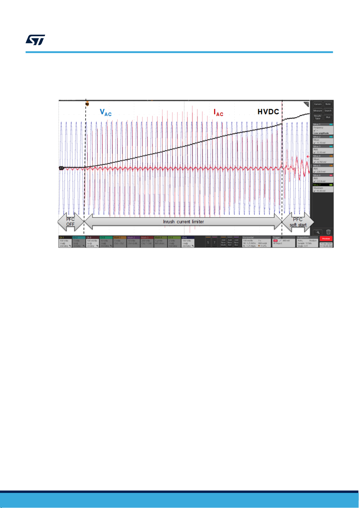
Figure 20. Inrush current control at board startup (with variable SCRs on delay)
HVDC=PFC output voltage
IAC = AC line current
VAC = AC line voltage
UM2792
Inrush current control
The look-up table listing the steps of SCRs turn-on delay reduction is defined by the TAB_SCRs_Delay_us table
in the ICL_Current_Constant.h file.
Note: The look-up table has been defined without DC load connected at the output PFC.
5.3.4 Inrush current control flowchart
SCRs are controlled to limit the inrush current at board startup (refer to Figure 21).
At each AC line voltage zero cross (see Figure 22. ICL flowchart (1 of 2) and Figure 23. ICL flowchart (2 of 2)):
• SCRs are switched to OFF state
• a timer is initialized to reduce SCR control turn-on delay from half-cycle to half-cycle
• test end of ICL procedure is performed:
– to check if the SCR turn-on delay is lower than 3 ms, the SCR gate pulse is directly set to a continuous
DC pulse according to the AC line polarity (SCR1 is set to continuous DC pulse when the AC line
polarity is negative and SCR2 is set to continuous DC pulse when the AC line polarity is positive). In
the firmware, the SCR turn-on delay is called Phase_Control_ON_Max_us.
– to check if the HVDC output DC voltage are charged at least 70% of the peak AC line voltage. In the
firmware, this value is called VAC_Rate_ICL_Min.
At each timer interrupt:
• SCRs are controlled according to the AC line voltage polarity
• the SCR control turn-on delay decreases
UM2792 - Rev 1
page 22/101
Page 23
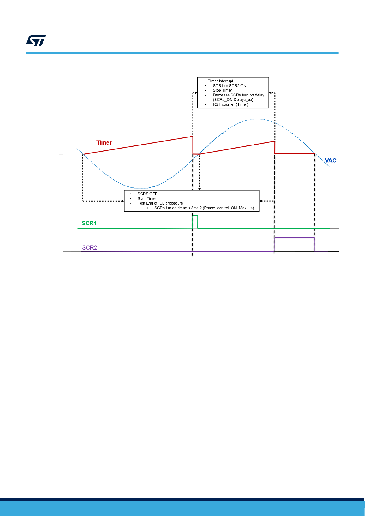
Figure 21. SCR control management
UM2792
Inrush current control
UM2792 - Rev 1
page 23/101
Page 24
Figure 22. ICL flowchart (1 of 2)
UM2792
Inrush current control
UM2792 - Rev 1
page 24/101
Page 25
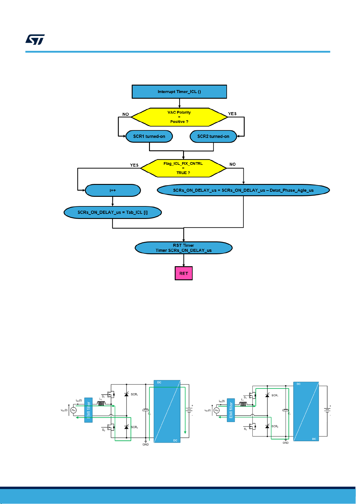
Figure 23. ICL flowchart (2 of 2)
UM2792
Steady state operation
5.4 Steady state operation
The bridgeless PFC totem pole increases its efficiency by eliminating the diode bridge in the conventional PFC.
It uses two SiC MOSFETs (S1 and S2) that operate at fixed PWM frequency and two SCRs (SCR1 and SCR2)
which operate at AC line frequency.
During the positive AC line cycle, SCR2 is always ON and SCR1 is always OFF. S1 and S2 are controlled in
synchronous mode. S1 and S2, together with the input inductor L1 and the output capacitor C1, form a boost
converter topology. S2 switch increases the boost inductor current and S1 acts as freewheeling boost diode.
[0 ; d.TS] on the left
[d.Ts ; TS] on the right
Figure 24. Positive AC line cycle operation
UM2792 - Rev 1
page 25/101
Page 26
During the negative AC line cycle, SCR1 is always ON and SCR2 is always OFF. S1 and S2 are controlled in
synchronous mode. S1 and S2, together with the input inductor L1 and the output capacitor C1, form a boost
converter topology. S2 switch increases the boost inductor current and S1 acts as a freewheeling boost diode.
Figure 25. Negative AC line cycle operation
[0 ; d.TS] on the left
[d.Ts ; TS] on the right
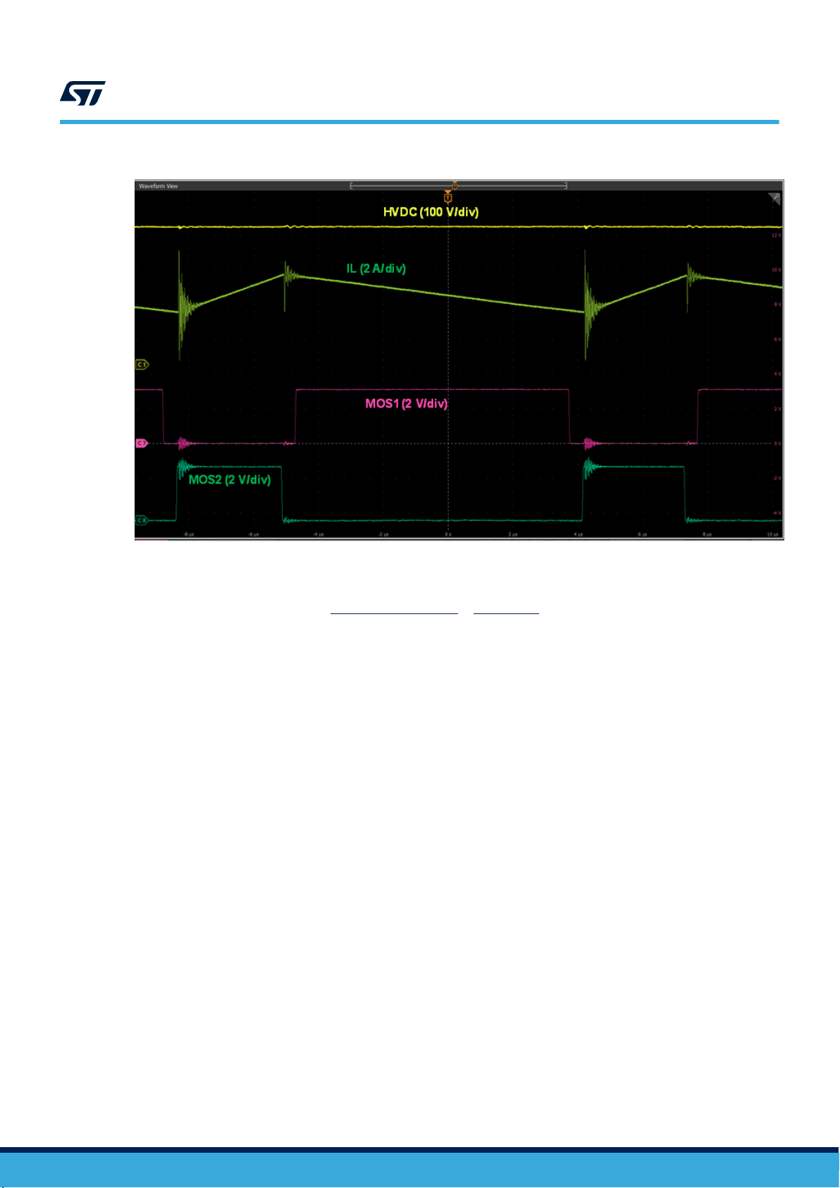
The following figure shows an example of the PFC totem pole behaviour in steady state operation with a 3.6 kW
DC load and VAC = 230 V
RMS
.
Note: Under the previous conditions, the HVDC peak to peak ripple is around 15 V.
UM2792
PFC soft start
HVDC = PFC output voltage
IAC = AC line current
VAC = AC line voltage
Figure 26. Steady state operation
5.5
UM2792 - Rev 1
PFC soft start
After the inrush current control procedure, the internal voltage loop output increases from initial voltage under the
soft start control to reduce the current stress due to all power switches. Once HVDC has reached 400 VDC, the
soft start control is released to achieve the desired regulation.
page 26/101
Page 27
HVDC = PFC output voltage
IAC = AC line current
VAC = AC line voltage
UM2792
PFC soft start
Figure 27. PFC soft start
Figure 28 shows how the PFC soft start is managed after the inrush current control procedure. The soft start PFC
management routine is called at each zero cross of the AC line voltage (see Figure 29). This routine increases the
HVDC output voltage target up to 400 VDC.
Figure 28. PFC startup soft start management after inrush control procedure
UM2792 - Rev 1
page 27/101
Page 28
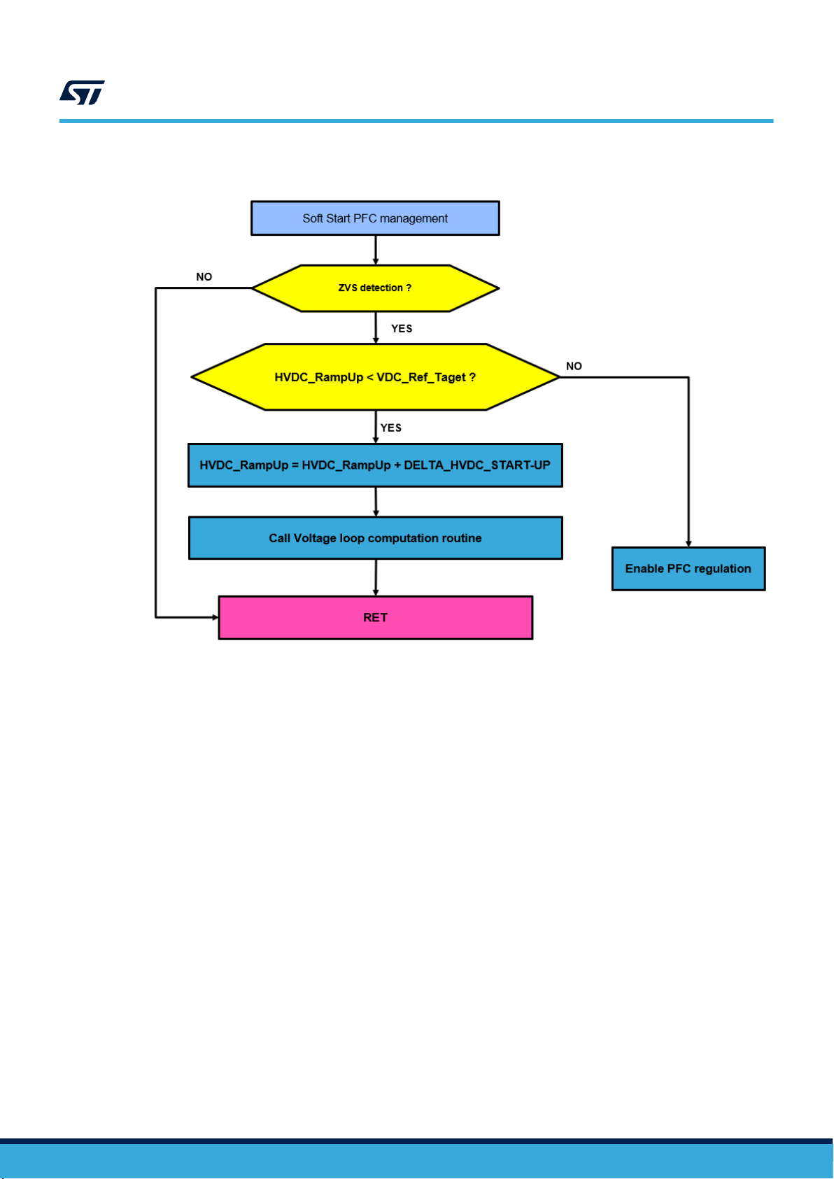
Figure 29. PFC startup soft start flowchart
UM2792
PFC soft start
UM2792 - Rev 1
page 28/101
Page 29
6 Switch control
6.1 SiC MOSFET control
A digital PWM signal is used to control SiC MOSFETs though STM32 timer (TIM1). Digital TIM1 counter period
is defined by Equation 2 where Fs is the PWM frequency fixed at 72 kHz and F
frequency fixed at 72 MHz.
Note: The duty cycle of the PWM control is defined by the STM32 TIM1 CCR2 register.
TIM1
Counter_Period
F
CPU
=
=
F
s
72 × 10
72 × 10
6
= 1000
3
The Duty cycle is clamped at the minimum (100 pulses) and the maximum (970 periods) of the digital TIM1 timer
counter.
To improve the PFC totem pole bridgeless efficiency, S1 and S2 SiC MOSFETS are operating in synchronous
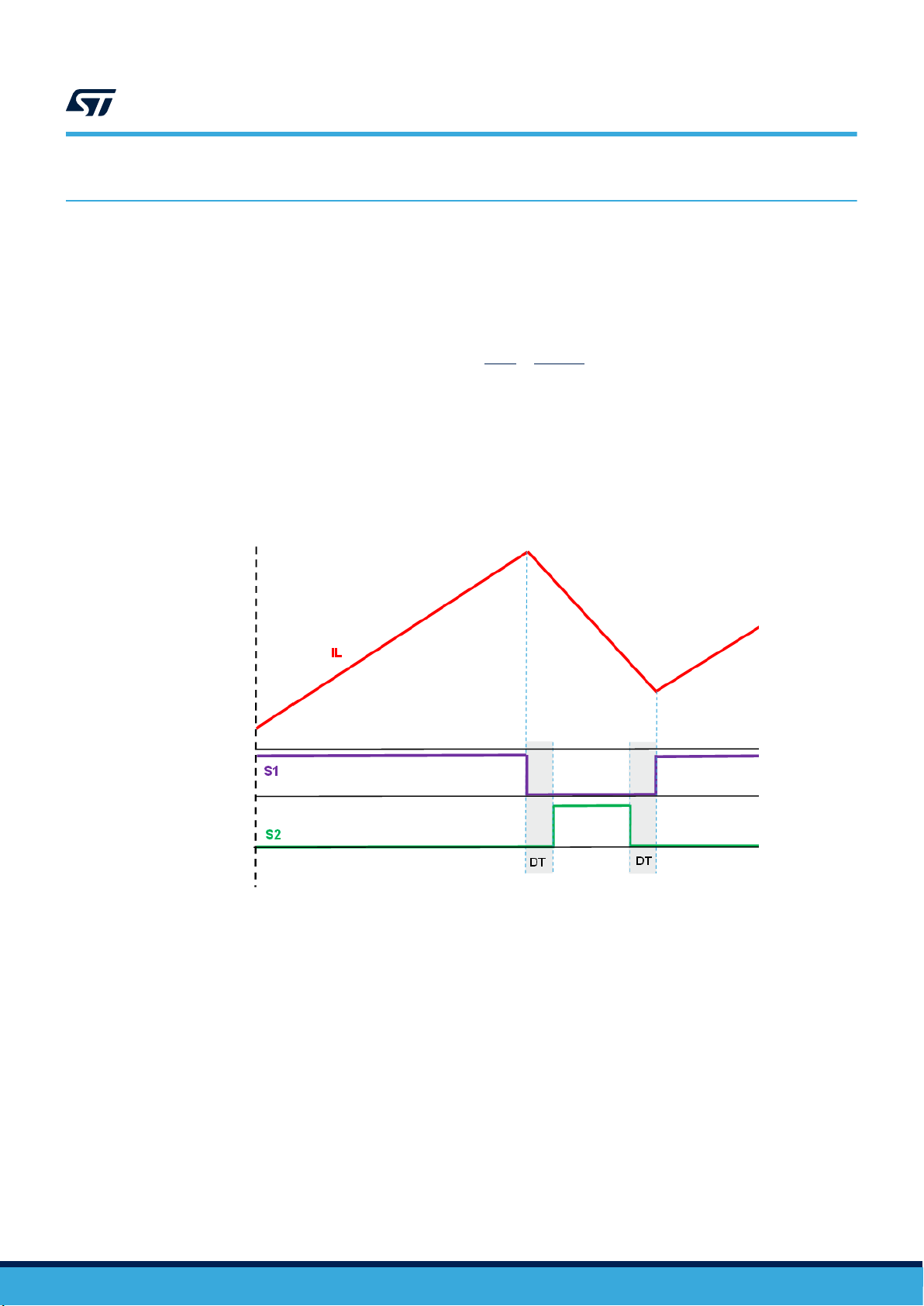
conduction mode. Two complementary PWM signals (CH2 and CH2N) are used to control SiC MOSFETs. To
avoid the short circuits due to a slight turns ON and OFF of SiC MOSFETs, a dead time (DT) has been added
(see the following figure) with IL as the inductor current.
Figure 30. Synchronous SiC MOSFET control
CPU
UM2792
Switch control
is the STM32 oscillator
(2)
UM2792 - Rev 1
page 29/101
Page 30
Zero cross current spike control
Figure 31. Synchronous SiC MOSFET control waveform
UM2792
The digital dead time is called “DeadTime_MOSFET” in the firmware and this parameter is fixed at 20 periods of
the TIM1 Timer.
DT =
DeadTime
Fs⋅ TIM1
Counter_Period
6.2 Zero cross current spike control
An input current (IAC) spike is generated at each AC line zero cross (VAC). This issue is related to the PFC totem
pole. For example, during the negative AC line cycle, SCR1 is always on and SCR2 is always off and the PFC
output voltage (400 VDC) is applied across SCR2. S1 SiC MOSFET switch increases the boost inductor current
and S2 SiC MOSFET acts as a freewheeling boost diode. When the AC line voltage polarity is changing from
negative to positive AC line cycle, the duty cycle of the S1 SiC MOSFET changes from 100% to zero and the
active S2 SiC MOSFET change from zero to 100%. The SCR1 voltage is then applied across the boost inductor
and current spike is generated (see Figure 32 and Figure 33). The same phenomenon occurs with diodes or
MOSFETs.
MOSFET
20
=
72000 ⋅ 1000
= 278 ns
(3)
UM2792 - Rev 1
page 30/101
Page 31

Figure 32. PFC totem pole topology
LOAD
S
1
V
AC
I
AC
SCR
1
SCR
2
S
2
HVDC
UM2792
Zero cross current spike control
Figure 33. IAC current spike at each AC line voltage zero crossing
To reduce this current spike at each zero cross of the AC line voltage, S1 or S2 active switches (according to the
AC line polarity) are controlled by a small pulse width. This pulse is then gradually increased up to normal duty
cycle.
UM2792 - Rev 1
page 31/101
Page 32

Figure 34. Smart duty cycle control flowchart
DUTY_CYCLE > DUTY_CYCLE_MAX
?
RET
FLAG_DUTY_CYCLE_SOFT = TRUE ?
STEP = RESET
NO
DUTY CYCLE = DUTY_CYCLE_MIN + 100 x STEP
STEP = STEP + 1
DMA_CH1 Interrupt()
YES
DUTY CYCLE = DUTY_CYCLE_MAX
YES
NO
UM2792
Zero cross current spike control
Figure 35. Soft duty cycle control principle
duty cycle control, the control loop is frozen.
The following figures show how the AC line current spike peak is reduced thanks to this solution. During the smart
Note: At each zero cross of the AC line voltage, SCRs and SiC MOSFETs are turned off to ensure a safe permutation
of the power switches control and to avoid short-circuiting the output DC capacitor.
UM2792 - Rev 1
page 32/101
Page 33
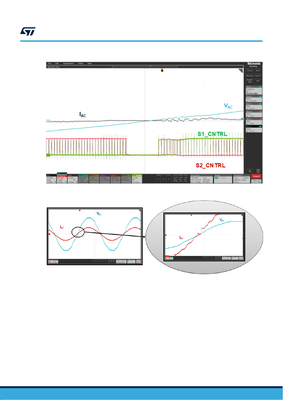
Figure 36. Smart duty control principle
UM2792
Zero cross current spike control
Figure 37. IAC current spike at each AC line voltage zero crossing
Figure 38 defines the common mode noise without smart duty cycle control and Figure 39 defines the common
mode noise with smart duty cycle control with P
= 800 W and VAC = 240 V
OUT
/50 Hz. Thanks to a smart duty
RMS
cycle SiC MOSFET control, the common mode is widely reduced at each zero cross of the AC line voltage.
Note: For these two common mode noise measurements a snap ferrite has been connected to the AC line wires (Ref:
742 758 15 from Wurth).
UM2792 - Rev 1
page 33/101
Page 34

Zero cross current spike control
Figure 38. Common mode without smart SiC MOSFET control
UM2792
Figure 39. Common mode with smart SiC MOSFET control
UM2792 - Rev 1
page 34/101
Page 35

7 PFC totem pole design
7.1 Input inductor design
The PFC choke is designed to keep the inductor current ripple under 20% of the maximum peak input current in
CCM (16 A
duty cycle of S1 and S2 SiC MOSFETs. The minimum inductor value is defined when D = 0.5 (see Eq. (3)). HVDC
is 400 VDC output voltage and Fs is the 72 kHz frequency switching of S1 and S2 Sic MOSFETs.
To meet the previous criterion with 10% of inductance tolerance, a 337 µH inductor has been selected for this
PFC totem pole at the maximum peak input current in CCM (16 A
). Equation 4 defines the minimum inductance to operate in CCM at full load (3.6 kW). D is the
RMS
D × 1 − D × HVDC
L ≥
I
L_Ripple_ %
Figure 40. PFC estimated nominal inductance vs. current
× F
0.5 × 1 − 0.5 × 400
=
s
0.2 × 16 × 2 × 72 × 10
RMS
).
= 307μH
3
UM2792
PFC totem pole design
(4)
7.2 Output DC capacitor
The output DC capacitor is defined by the equations below according to the hold time and output voltage ripple
regulation. In this evaluation board, the hold time is set to 1 half AC line cycle (45 Hz in the worst case). HVDC is
400 VDC output voltage, the minimum normal operation output voltage is 290 V, the maximum input power is 3.6
kW and the output voltage ripple is set to 5%.
C
≥
OUT
C
To meet the previous criteria with 20% of capacitor tolerance, 3 x 680 µF/450 VDC electrolytic capacitors are
connected in parallel.
UM2792 - Rev 1
P
2 × π × f × HVDC × HVDC
≥
OUT
OUT
2 × P
HVDC2− HVDC
OUT
× t
ℎold
min
Ripple
2
=
2 × π × 45 × 400 × 20
2 × 3600 ×
=
4002− 290
3600
1
2 × 45
2
= 1.59mF (5)
= 1.05mF
(6)
page 35/101
Page 36

7.3 Analog signal sensing
2
Vcc-
3
In-
R17
A_GND
470k
68nF
470k
A_GND
C14
R18
U2
R22
470k
K
2
3V3_A
MCP6231UT-E/OT
A_GND
470k
R23
R24
5
10k
U1
100nF 4.7uF
L1
470k
C20
NC
1
In+
R21
COM
3
470k
VAC_SENSE
C9
Vcc+
Out
4
C8
C12
NC
N1
C15
3.9nF
R27
R29
470k
R35
5k
470k
A_GND
A
1
R16
470k
R31
R28
3V3_A
A_GND
68nF
10k
7.3.1 AC line voltage (VAC) measurement
The AC line voltage (VAC) measurement is mainly used to:
• control the inrush current at board startup
• shape the IAC line current to the AC line voltage in PFC steady state operation
• detect the zero cross of the AC line voltage
• manage the AC line dips
A differential measurement is performed to measure VAC based on the line voltage (VL) and the neutral voltage
(VN) measurements (VAC = VL - VN). To sense VL and VN, a resistor divider bridge is used. The typical voltage
sensor is 3.545 mV/VAC.
Figure 41. AC line voltage measurement
UM2792
Analog signal sensing
7.3.2 AC line current (IAC) measurement
The PFC choke inductor current is measured to shape the AC line current to the AC line voltage. A CASR
15-NP current transducer is used in series with the PFC choke as shown in the figure below. The typical current
transducer is 41.6 mV/IAC.
As the AC line current is an alternative signal, an offset is needed to be read by the MCU. The current transducer
sensor is supplied with 5 VDC. R3 resistor (1.3 kOhms) is connected to the VREF pin of the current transducer
UM2792 - Rev 1
sensor to set the offset to 1.64 VDC.
page 36/101
Page 37

Figure 42. PFC choke inductor current sensor
150pF
A_GND
+
-
10k
10k
40k
10
9
OUT2
C31
1.3k
8
A_GND
40k
12
GND
150pF
R43
IAC_OFFSET
4.7uF
R41
NC
IN1
1
C44
OUT3
IM2
150pF
IN3
3
13
VC
14
5V_A
IAC_SENSE
A_GND
C38
VREF
11
U28
C29
C46
680INT_REF
LEM CASR 15-NP
2
IN2
OUT1
100nF
VOUT
Rm
R59
160k
C59
A_GND
U4
3V3_DC
160k
3k
K
2
GND_DC
160k
10nF
GND_DC
R54
A
1
HVDC
C60
NC
NC
NC
R50
C33
3
COM
R51
UM2792
Analog signal sensing
7.3.3 Output PFC HVDC measurement
A resistor divider circuit is used to measure the output PFC voltage (HVDC). As the MCU ADC input port is a high
resistance, an amplifier is not needed. The typical voltage sensor is 6.2 mV/HVDC.
UM2792 - Rev 1
Figure 43. HVDC output measurement
page 37/101
Page 38

7.3.4 Signal sense filter
Q2
5V_SCR1
R45
1k
C58
R44
1
GND_SCR1
390R
R55
2
270R
270R
R47
2N2907A
R52
R58
GND_SCR1
C52
4 1
10nF
G_SCR2
10nF
3
U6
R56
2N2907A
390R
GND_DC
100R
R46
R48
C53
LTV-817
5V_SCR2
C51
3
Q3
10nF
R53
1k
R57
G_SCR1
GND_DC
10nF
4
390R
SCR1
LTV-817
R49
GND_SCR2
U7
C57
100R
GND_SCR2
2
SCR2
100nF
47R
100nF
390R
C56
An RC filter is used to filter all analog signals (VAC, IAC, HVDC, TEMP).
7.4 Power circuit driver
7.4.1 SCR control circuit
The VIPER26LD flyback provides two insulated DC output voltage to control SCR1 and SCR2. Insulated positive
power supplies are required to supply current to SCR gates. As the MCU is not at the same ground reference as
SCRs, optocouplers are needed as shown in the figure below.
To improve the circuit control immunity filters have been added:
• an RC filter connected between the base and the emitter of the PNP transistors (Q2 and Q3)
• R45/R53 = 1 kΩ
• C52/C57 = 10 nF
• capacitors (C53 and C58) associated with R46/R47 and R55/R56 resistors improve the immunity of the
optocouplers (U6 and U7)
UM2792
Power circuit driver
Figure 44. SCR insulated control
UM2792 - Rev 1
To define the resistor value of the SCR control circuit, the block of equations below define the new resistor
definition according to the previous figure.
RGK= R44= R
Rg= R49= R
RF1= R45= R
RF2= R47= R
RF3= R46= R
RL= R48= R
CF1= C52= C
CF2= C53= C
52
58
53
56
55
57
57
58
Knowing the SCR gate current (IGT), the gate resistor RGK to limit the SCR gate current can be defined according
to the equation below, where 5VSCR is the power supply to provide the gate current to the SCRs, VCE_SAT
is the transistor collector/emitter of the PNP transistors (Q2 and Q3), VGT is the SCR gate triggering voltage and
RGK is the gate cathode resistor used to increase the SCR immunity.
PNP
page 38/101
(7)
(8)
(9)
(10)
(11)
(12)
(13)
(14)
Page 39

UM2792
Power circuit driver
5V
Rg<
SCR
IGT
SAT_PNP
SCR
− VCE
The collector resistors (RF2 and RF3) of the optocoupler are defined by the equation below, where RF1 is
the PNP transistor resistor filter, VCC_AC is the power supply to provide the gate current to the AC switch,
VCE_SAT
is the transistor collector/emitter of the optocoupler, β is the PNP transistor gain and VBE_SAT
Opto
is the PNP transistor base/emitter.
RF2+ RF3=
5V
SCR
SCR
− VCE
SAT_OPTO
SAT_NPN
β ⋅ R
G
5V
− VCE
Knowing the optocoupler CTR, RF2 and RF3 resistors value, the LED resistor RL of the optocoupler is defined
by the equation below, where 5VSCR is the power supply to provide the gate current to the AC switch,
VCE_SAT
is the transistor collector/emitter of the optocoupler, VBE_SAT
Opto
emitter and VOH_Min_MCU is the output MCU voltage to drive the optocoupler.
RL=
1
CTR
VOH_Min_MCU − VF
VCC_AC − VCE_SAT
×
With LTV-817 optocoupler and 2N2907 PNP transistor, you have to choose the following resistor values.
RGK= R44= R52= 1kΩ (18)
Rg= R49= R58= 47kΩ (19)
RF1= R45= R53= 1kΩ (20)
RF2= R47= R56= 390kΩ (21)
RF3= R46= R55= 390kΩ (22)
RL= R48= R57= 1kΩ (23)
CF1= C52= C57= 10nF (24)
CF2= C53= C58= 10nF (25)
VGT
+
R
− VGT_SCR
Opto
RF2+ R
− VGT
SCR
GK
− VBE
Opto
− VBE_SAT
F3
SCR
SAT_PNP
VBE
+
SAT_PNP
R
F1
is the PNP transistor base/
PNP
PNP
(15)
PNP
(16)
(17)
7.4.2 SiC MOSFET control circuit
The STGAP2S driver is designed to drive ST SiC MOSFET providing high peak current during turn-on and turn-off
and to minimize the switching losses for better system efficiency and EMI.
SiC MOSFET switches have different requirements for gate turn-on and turn-off voltage levels. The turn-on
voltage level is performed with +20 VDC and the turn-off is operated with -3.3 VDC to ensure the gate source safe
operating area.
UM2792 - Rev 1
page 39/101
Page 40

Figure 45. STGAP2S driver
24R
1nF
C41
8
100nF
U3
100nF
C21
C42
1uF
C22
GND_S2
VH
5
GND_DC
100nF
D3
NC
4.7uF
C24
GON
6
C39
2
IN+
STGAP2SM
L16
2A
150pF
C40
R42
NC
2
D6
NC
GON
6
GND_S2
24R
R40
8
1nF
GND_S2
150pF
C19
C30
R34
L15
D4
1
VDD
MOS1
3V3_DC
3
IN-
C18
C35
C26
2.2nF
3V3_DC
-3V_S2
R38
10k
1uF
NC
C36
100nF
G_MOS1
3
IN-
GND_S1
10k
24R
510R
G_MOS2
4.7uF
R39
GND_ISO
2.2nF
C28
4
GND
MOS2
C43
R32
VH
5
C27
1uF
150pF
GND_S1
-
20V_S1
C23
GND_ISO
7
GOFF
20V_S2
C25
U5
D5
150pF
R36
C45
VDD
1
GND_DC
GND_S1
2A
7
GOFF
C34
R33
1uF
1uF
1uF
IN+
STGAP2SM
4
GND
24R
510R
3V_S1
+VIN
10nF
C118
C107
GND_DC
C120
60R
C105
33uF/25V
33uF/25V
D18
C117
C104
2
39 mH
2A
R94
U15
100nF
20V_S2
R90
+
C126
-VIN
6
-Vout
0V
R89
2
+VIN
7
MGJ2D122005SC
20V_S1
DZ2W03300L
10nF
C114
C125
C119
+
L9
C102
+
C116
-3V_S2
1
1
60R
12V_DC
60R
L12
C103
C101 33uF/25V
-3V_S1
C115
5
100nF
39 mH
100nF10nF
D19
60R
+
5
2A
R95
MGJ2D122005SC
100nF
GND_S1
60R
C113
22uF/25V
DZ2W03300L
L13
C106
L7
GND_DC
+Vout
U16
60R
33uF/25V
R87
10nF
R93
22uF/25V
60R
100nF
100nF
7
R88
+Vout
6
C112
-VIN
-Vout
0V
100nF
R96
60R
100nF
UM2792
Power circuit driver
UM2792 - Rev 1
The asymmetric SiC MOSFET gate voltages (+20 VDC/-3.3 VDC) are achieved thanks to a high insulated DC-DC
converter (MGJ2 series from MURATA) to power the high side and the low side gate drive circuits for SiC
MOSFETs.
Figure 46. STGAP2S driver - DC-DC converter
page 40/101
Page 41

8 PFC protections
OFFSET
IL
t
OVP_H
OVP_L
8.1 Analogue overcurrent protection
Two comparators are used to detect the positive and negative PFC choke inductor overcurrent. This I
overcurrent detection is achieved thanks to STM32 comparators (COMP2 and COMP4) and STM32 digital analog
converters (DAC CH1 and DAC CH2).
Figure 47. STM32 comparator configuration
UM2792
PFC protections
AC
Figure 48. Positive and negative overcurrent detection
UM2792 - Rev 1
page 41/101
Page 42

An interrupt is generated by COMP2 or COMP4 peripherals if the PFC inductor current image is higher than
OVP_H limit or lower than lower OVP_L limit, respectively. Upper limit (OVP_H) and lower limit (OVP_L) are
defined by the STM32 digital analog converter peripherals (DAC CH1 and DAC CH2). The equations below define
the digital upper and lower limit with IAC_OFFSET the digital value (2070) of the IAC current sensor offset value.
The PFC totem pole turns off if the maximum PFC choke inductor current is higher than 25 A peak.
DAC
DAC
CH1
CH2
n
2
=
× I
ref
2
ref
L_MAX
n
× I
L_MAX
V
=
V
ΔI
L
+
× K
2
ΔI
L
+
× K
2
8.2 Digital PFC choke inductor current clamping
The PFC totem pole has been designed to limit the AC line current at 16 A
current is clamped to 16 A
performed by clamping the peak current reference in the firmware. The PFC totem pole board switches off if the
HVDC voltage is lower than the peak AC line voltage measured at board startup.
, if the output DC current (IDC) increases, the HVDC voltage decreases. This is
RMS
Figure 49. Over input current protection
i_sense
i_sense
UM2792
Digital PFC choke inductor current clamping
+ I
AC_OFFSET
− I
AC_OFFSET
(IAC). In this case, as the input
RMS
(26)
(27)
UM2792 - Rev 1
page 42/101
Page 43

Figure 50. IAC inductor current clamp
390 Vdc
MOSFETs ON
400 Vdc
HVDC
Load variation
420 Vdc
450 Vdc
MOSFETs OFF
MOSFETs ON
UM2792
HVDC overvoltage protection
8.3 HVDC overvoltage protection
HVDC output overvoltage might occur with a DC load variation from high to light load. SiC MOSFETs are switched
off if the HVDC output voltage is higher than 420 VDC and switched on again if the HVDC output voltage is lower
than 390 VDC at the zero cross of the AC line voltage.
Figure 51. Overvoltage protection
8.4 Overtemperature protection
The PFC totem pole temperature protection is made with a TO-220 temperature sensor mounted on the heatsink
and connected to an MCU GPIO. If overtemperature is detected by the MCU, the PFC totem pole turns off.
UM2792 - Rev 1
page 43/101
Page 44

9 Control loop design
9.1 Timing diagram
The AC line voltage (VAC), the PFC chock current (IL) and HVDC output voltage are sampled at the center of the
PWM signal used to control SiC MOSFET switches. The inner current loop computation is executed at 72 kHz to
get the desired switching signal and configured accordingly. The outer voltage loop computation is executed at
each AC line zero crossing.
UM2792
Control loop design
Figure 52. Timing diagram
9.2
UM2792 - Rev 1
Digital power factor correction (DPFC)
The figure below shows the PFC totem pole regulation principle using a digital control implemented in the STM32
microcontroller:
• the outer voltage loop regulates the totem pole HVDC output voltage
• the current loop is the faster loop and is used to shape the current inductor to the sinusoidal reference
(I
)
L_REF
• PLL is used to synchronize the PFC to the AC line cycle
page 44/101
Page 45

Figure 53. Digital PFC control diagram
Ci(s)
KcADC
I
Hi(s) =
L_MES
-
+
d
DPWM
L
I
L_REF
i
d(s)
L
(s)
UM2792
Current loop control design
9.3 Current loop control design
9.3.1 Current loop model
The figure below shows the current loop small signal model block diagram. The current loop controller keeps the
error between the reference and the current inductor at zero.
Ci(s) = current loop controller
Hi(s) = current transfer function duty cycle
DPWM = digital PWM gain
ADC = ADC transfer function
kc = current sensor transfer function to measure PFC choke inductor current
IL_REF = current reference signal
Figure 54. Current loop diagram
UM2792 - Rev 1
The controller output is fed by the DPWM block to control SiC MOSFET. The duty cycle adapts the inductor
current to be in phase with the reference signal (I
The full transfer function of open current loop is defined by the following equation
Tis = Cis × His × ADC × DPWM × K
The PFC duty cycle of current transfer function is defined by
L_REF
).
c
page 45/101
(28)
Page 46

UM2792
Current loop control design
R ⋅ C
His =
ILs
d s
2 ⋅ HVDC
=
R ⋅ 1 − d
⋅
2
1 +
E
R ⋅ 1 − d
1 +
L
In high frequency:
ILs
His =
d s
=
HVDC
L ⋅ s
with
2
HVDC
R =
POUT
and duty cycle equilibrium point:
dE= 1 −
VAC
HVDC
where:
• POUT: PFC output power
• L: PFC boost inductance
• C : DC output capacitor
• VAC: Input AC line voltage
• HVDC : DC output voltage
The current loop controller Ci(s) is defined by the following equation with Kp_i and Ki_i PI controller analog
coefficients
Cis = K
p_i
K
i_i
+
= K
s
p_i
1 + τi× s
×
with
K
p_i
τi=
K
i_i
The current sensor sensitive coefficient is defined by
Kc= 0.0416
The ADC STM32 transfer function is defined by
n
12
2
ADC =
V
ref
2
=
= 1241
3.3
The Digital PWM gain based on 72 MHz timer resolution and a 72 kHz switching frequency (Fs_i) is defined by
DPWM =
F
s_i
F
CLK_MCU
=
72 × 10
72 × 10
3
6
2
⋅ s +
2
E
τi× s
= 1 × 10
⋅ s
1 − d
−3
L ⋅ C
2
⋅ s
2
E
(29)
(30)
(31)
(32)
(33)
(34)
(35)
(36)
(37)
9.3.2 Controller design
A good current loop performance needs the crossover frequency F
switching frequency. To ensure the stability of the loop, two criteria must be verified with PMi as phase margin.
According to the previous equations, τi, Kp_i and Ki_i analog coefficients are defined by
In bilinear transformation, the formula below is used
UM2792 - Rev 1
20 × log Tis = 1 (38)
arg Tis = + 180 + PM
tan PM
τi=
2 × π × F
K
=
p_i
HVDC × ADC × DPWM × Kc× 1 + τi× 2 × π × F
L × τi× 2 × π × F
K
i_i
s =
T
i
c_i
K
p_i
=
τ
i
2
z − 1
×
z + 1
s
to be around 15 time lower than the
C_i
i
2
c_i
c_i
2
(39)
(40)
(41)
(42)
(43)
page 46/101
Page 47

UM2792
Feedforward design
The current loop controller Ci(z) is defined by
K
⋅ T
p_i
s_i
− K
2 ⋅ τ
Ciz =
i
where
K
τi=
According to the previous equations Kpz_i and Kiz_i are defined by
K
= K
iz_i
−
p_i
=
2 × τi× F
pz_i
K
Note: The current loop is executed at the MOSFETs switching frequency and fixed at 72 kHz. Ts_i and Fs_i are
repectively the MOSFETs switching period and the MOSFETs switching frequency.
To thoroughly use MCU resources, the PI corrector coefficients are normalized to fixed-point decimal format (Q15
data format). The relation between the actual and normalized values is defined by
K
pz_i_Q15
K
iz_i_Q15
= K
= K
To optimize the HVDC regulation, the PI current loop coefficient has been defined according to the AC line
voltage.
The table below defines the controller coefficient to be set in the MCU. In the firmware:
• the integral gain is defined by “PI_IAC_KI_230” and “PI_IAC_KI_110” according to the AC line voltage range
• the proportional gain is defined by “PI_IAC_KP_230” and “PI_IAC_KP_110” according to the AC line voltage
range
K
⋅ T
p_i
2 × τ
s_i
i
s_i
⋅ z
+
p_i
−1 + z
p_i
K
i_i
K
p_i
2 × τi× F
K
p_i
s_i
× 8192 (48)
pz_i
× 8192 (49)
iz_i
(44)
(45)
(46)
(47)
Table 10. Integral and proportional gains of the current loop PI controller
Parameter
Kpz_i_Q15 3400 3400
Kiz_i_Q15 40 260
9.4 Feedforward design
When the main voltage or load current changes suddenly, the low bandwidth of the voltage loop may cause
output voltage fluctuations. To alleviate the feedback controller, a digital feedforward control (DFF) has been
included in the current loop to pre-calculate a duty ratio as defined by the equation below where HVDC is the PFC
output voltage and VAC the AC is the line voltage.
The feedforward duty ratio is added to the average current mode control output to generate the final duty ratio.
The regular current loop compensator changes the duty ratio around this calculated duty ratio pattern.
VAC = 110 V
P
OUT_MAX
dFF=
RMS
= 1.8 kW
HVDC − VAC
HVDC
VAC = 230 V
P
OUT_MAX
RMS
= 3.6 kW
(50)
UM2792 - Rev 1
page 47/101
Page 48

10 Voltage loop control design
10.1 Voltage loop model
The figure below shows the small signal model block diagram.
Figure 55. Voltage loop diagram
Cv(s) = voltage loop controller
Hv(s) = inductor current to output voltage transfer function
ADC = ADC transfer function
kv= inductor current transfer function
UM2792
Voltage loop control design
The full transfer function of open voltage loop is defined by
Tvs = Hvs × Cvs × ADC × K
v
The output voltage transfer function is defined by
Hvs =
VAC⋅ R
2 ⋅ HVDC ⋅ Kc⋅ ADC
1
×
R ⋅ C
1 +
⋅ s
2
with
2
HVDC
R =
POUT
where:
• POUT: PFC output power
• C : The DC output capacitor
• VAC: Input AC line voltage
• HVDC : DC output voltage
• Kc = 0.0416 (current sensor sensitive coefficient)
The voltage loop controller Cv(s) is defined by with Kp_v and Ki_v PI controller analog coefficients
Cvs = K
p_v
K
i_v
+
= K
s
p_v
1 + τv× s
×
τv× s
with
K
p_v
τi=
K
i_v
The output voltage sense gain is defined by
R
Kv=
2
R1+ R
= 0.0062
2
The ADC STM32 transfer function is defined by
n
12
2
ADC =
V
ref
2
=
= 1241
3.3
(51)
(52)
(53)
(54)
(55)
(56)
(57)
UM2792 - Rev 1
page 48/101
Page 49

UM2792
Controller design
The equivalent resistor on the PFC output with HVDC, the PFC output voltage and P
power are defined by
10.2 Controller design
A good current loop performance needs the crossover frequency F
switching frequency. To ensure the stability of the loop, two criteria must be verified with PMi as phase margin.
According to the previous equations, τv, Kp_v and Ki_v are defined by
In bilinear transformation, the formula below is used
The voltage loop controller Cv(z) is defined by
where
According to the previous equations Kpz_i and Kiz_i are defined by
τv=
tan PMi+ 90 × 2 × R × C × π2× F
4 × HVDC × Kv× π × F
K
=
p_v
Cvz =
HVDC
R =
P
20 × log Tvs = 1 (59)
arg Tvs = + 180 + PM
R × C × F
VAC× VR× R × Kv×
K
⋅ T
p_v
2 ⋅ τ
v
K
pz_v
s_v
= K
K
iz_v
K
s =
− K
i_v
τv=
p_v
=
c_v
c_v
=
2
T
s
p_v
−
2 × τv× F
2
OUT
to be around 15 time lower than the
C_v
i
− tan PMi+ 90
2
+ 2 × π × F
c_v
× τv× 1 + R × C × π × F
1 + τi× 2 × π × F
K
p_v
τ
v
z − 1
×
z + 1
K
⋅ T
p_v
+
2 × τ
−1 + z
K
p_v
K
i_v
K
p_v
2 × τv× F
K
s_v
p_v
s_v
s_v
v
+ K
c_v
p_v
c_v
2
⋅ z
c_v
, and the PFC output
out
2
(58)
(60)
(61)
(62)
(63)
(64)
(65)
(66)
(67)
(68)
Note: The voltage loop is executed at each zero cross of the AC line voltage. Fs_v is fixed at twice the AC line
frequency.
To thoroughly use MCU resources, the PI corrector coefficients are normalized to fixed-point decimal format (Q15
data format). The relation between the actual and normalized values is defined by
K
pz_v_Q15
K
iz_v_Q15
= K
= K
× 2048
pz_v
× 2048 (70)
iz_v
To optimize the HVDC regulation, the PI voltage loop coefficient has been defined according to the AC line
voltage.
The table below defines the controller coefficient to be set in the MCU. In the firmware:
• the integral gain is defined by “PI_VBUS_KI_230” and “PI_VBUS_KI_110” according to the AC line voltage
range
• the proportional gain is defined by “PI_VBUS_KP_230” and “PI_VBUS_KP_110” according to the AC line
voltage range
UM2792 - Rev 1
(69)
page 49/101
Page 50

Table 11. Integral and proportional gains of the current loop PI controller
UM2792
Controller design
Parameter
VAC = 110 V
P
OUT_MAX
RMS
= 1.8 kW
Kpz_v_Q15 2300 940
Kiz_v_Q15 500 400
VAC = 230 V
P
OUT_MAX
RMS
= 3.6 kW
UM2792 - Rev 1
page 50/101
Page 51

11 AC line zero crossing synchronization
ADC
VAC
PI
+
+
α
θ
/
Integral
α/β
d/q
d/q
α/β
wc
β
q
d
LPF
LPF
VAC
VRMS
Frequency
11.1 PLL loop control design
To track the frequency and phase of the AC line voltage, a phase-locked loop (PLL) is used. The block diagram of
this loop is defined in Figure 56 by using a low pass filter and a PI controller implemented in the STM32 firmware.
PLL is used to generate the current reference in phase with the AC line voltage to shape the input AC line current
to the AC line voltage.
Figure 56. PLL diagram
UM2792
AC line zero crossing synchronization
The PLL is a closed loop system where the phase error between the PLL output phase and the reference is
minimum. In steady state, the PLL output generates a sinusoidal wave close to the AC line voltage. A PI controller
is used to reduce the error between the reference and the Vq value measured. Vq is defined thanks to the Park
transformations of AC line voltage.
In steady state operation, the PLL and the grid frequency are closed. The simplified system for the PLL is defined
by the following figure.
Figure 57. PLL loop PI controller
The input voltage sense gain is defined by
The ADC STM32 transfer function is defined by
K
VAC_sense
ADC =
n
2
=
V
ref
= 0.003545
12
2
= 1241
3.3
(71)
(72)
UM2792 - Rev 1
page 51/101
Page 52

The full transfer function of open loop is defined by
T
PLL s
= Vm ⋅ Kp
PLL
1 + τ
⋅
τ
PLL
PLL
⋅ s
1
⋅
s
⋅ s
The current loop controller CPLL(s) is defined by the following equation with K
coefficients
C
PLL
s = K
p_PLL
1 + τ
×
τ
PLL
PLL
× s
× s
with
K
τ
PLL
p_PLL
=
K
i_PLL
The input voltage sense gain is defined by
K
VAC_sense
= 0.003545 (76)
The ADC STM32 transfer function is defined by
n
12
2
ADC =
V
ref
2
=
= 1241 (77)
3.3
Vm is defined by
Vm= VAC ⋅ Kv⋅ ADC (78)
p_PLL
and K
i_PLL
UM2792
Controller design
(73)
as analog
(74)
(75)
11.2 Controller design
A good current loop performance needs the crossover frequency F
stability of the loop, two criteria must be verified with PMi phase margin fixed at 45°C.
According to the previous equations, τ
K
p_PLL
In bilinear transformation, the formula below is used
The current loop controller CPLL(z) is defined by
According to the previous equations Kpz_i and Kiz_i are defined by
=
C
V
PLL
AC_Peak
z =
arg T
, K
PLL
× ADC × K
K
⋅ T
p_PLL
2 ⋅ τ
K
pz_PLL
K
20 × log T
PLL
p_PLL
τ
PLL
τ
PLL
VAC_Sense
K
i_PLL
s =
s_PLL
PLL
= K
iz_PLL
s = 1 (79)
PLL
s = + 180 + PM
and K
i_PLL
tan PM
× 1 + τ
=
2
×
s
K
K
−
K
p_PLL
τ
PLL
z − 1
z + 1
K
−1 + z
p_v
i_v
2 × τ
K
p_PLL
PLL
PLL
c_PLL
C_PLL
p_PLL
× F
=
2 × π × F
× 2 × π × F
T
− K +
τv=
p_PLL
=
2 × τ
to be fixed at 65 Hz. To ensure the
C_PLL
i
are defined by
2
× 2 × π × F
PLL
⋅ T
s_PLL
2 × τ
PLL
K
p_PLL
× F
PLL
s_PLL
s_PLL
+ K
C_PLL
p_PLL
= 0.546
2
⋅ z
(80)
(81)
(82)
(83)
(84)
(85)
(86)
(87)
(88)
Note: The PLL loop is executed at 9 kHz (Fs_PLL).
To thoroughly use MCU resources, the PI corrector coefficients are normalized to fixed-point decimal format (Q15
data format). The relation between the actual and normalized values is defined by
K
pz_PLL_Q15
UM2792 - Rev 1
= K
pz_PLL
× 2048
(89)
page 52/101
Page 53

UM2792
Controller design
K
iz_PLL_Q15
= K
× 2048 (90)
iz_PLL
To optimize the HVDC regulation, the PI PLL loop coefficient has been defined according to the AC line voltage.
The table below defines the controller coefficient to be set in the MCU. In the firmware:
• the integral gain is defined by “PI_PLL_KI_230” and “PI_PLL_KI_110” according to the AC line voltage range
• the proportional gain is defined by “PI_PLL_KP_230” and “PI_PLL_KP_110” according to the AC line voltage
range
Table 12. Integral and proportional gains of the current loop PI controller
Parameter
Kpz_PLL_Q15 1421 460
Kiz_PLL_Q15 30 10
VAC = 110 V
P
OUT_MAX
RMS
= 1.8 kW
VAC = 230 V
P
OUT_MAX
RMS
= 3.6 kW
UM2792 - Rev 1
page 53/101
Page 54

12 Experimental results
0
2
4
6
8
10
12
14
16
85
87
89
91
93
95
97
99
0 500 1000 30001500 2000 2500 3500 4000
THD (%)
Efficiency (%)
Output power (P
out
)
V
AC
= 230 V
RMS
- 50 Hz
12.1 Efficiency and THD
The figures below show the PFC totem pole efficiency and THD according to the output power (P
UM2792
Experimental results
).
out
Figure 58. PFC efficiency and THD for VAC = 230 V
Figure 59. PFC efficiency and THD for VAC = 110 V
RMS
RMS
/50 Hz
/60 Hz
UM2792 - Rev 1
page 54/101
Page 55

12.2 Load variation
HVDC
S1_CNTRL
S2_CNTRL
V
AC
I
AC
I
HVDC
2
The figure below shows the transient response of the PFC totem pole when the AC line voltage is 230 V
and the DC load current (IHVDC) is stepped up from 0 % to 100 % (see 1) and stepped down from 100 % to 0 %
(see 2).
UM2792
Load variation
(VAC)
rms
VAC = AC line voltage
IAC = AC line current
HVDC = PFC output voltage
IHVDC = PFC output current
Figure 60. Load variation with VAC = 230 V
RMS
/50 Hz
The figure below shows the transient response when the AC line voltage is 230 V
(VAC) and the DC load
rms
current (IHVDC) is stepped up from 50 % to 100 % (see 1) and stepped down from 100 % to 50 % (see 2).
UM2792 - Rev 1
page 55/101
Page 56

HVDC
S2_CNTRL
S1_CNTRL
V
AC
I
AC
I
HVDC
2
UM2792
PFC totem pole startup
Figure 61. Load variation with VAC = 230 V
VAC = AC line voltage
IAC = AC line current
HVDC = PFC output voltage
IHVDC = PFC output current
/50 Hz (stepped up/down to 50%)
RMS
12.3 PFC totem pole startup
The figure below shows the startup sequence of the PFC totem pole with VAC = 230 V
DC load.
Figure 62. PFC startup with VAC = 230 V
VAC = AC line voltage
IAC = AC line current
HVDC = PFC output voltage
/50 Hz and with a 1 kW
rms
/50 Hz and P
RMS
= 1 kW
out
UM2792 - Rev 1
The figure below shows the startup sequence of the PFC totem pole with VAC = 110 V
DC load.
/60 Hz and with a 1 kW
rms
page 56/101
Page 57

UM2792
Steady state operation
Figure 63. PFC startup with VAC = 110 V
VAC = AC line voltage
IAC = AC line current
HVDC = PFC output voltage
Figure 64. PFC startup with VAC = 110 V
VAC = AC line voltage
IAC = AC line current
HVDC = PFC output voltage
/60 Hz and P
RMS
/60 Hz and without DC load
RMS
out
= 1 kW
12.4
UM2792 - Rev 1
Steady state operation
The figures below show the PFC steady state current waveform at different load conditions.
page 57/101
Page 58

UM2792
Steady state operation
Figure 65. PFC steady state with VAC = 230 V
VAC = AC line voltage
IAC = AC line current
HVDC = PFC output voltage
Figure 66. PFC steady state with VAC = 230 V
VAC = AC line voltage
IAC = AC line current
HVDC = PFC output voltage
/50 Hz and Pout = 1 kW
RMS
/50 Hz and Pout = 2 kW
RMS
UM2792 - Rev 1
page 58/101
Page 59

UM2792
Mains voltage dips and interruptions
Figure 67. PFC steady state with VAC = 230 V
VAC = AC line voltage
IAC = AC line current
HVDC = PFC output voltage
/50 Hz and Pout = 3 kW
RMS
12.5 Mains voltage dips and interruptions
12.5.1 IEC 61000-4-11 standard
IEC 61000-4-11 standard defines the test conditions to evaluate the immunity of the equipment to a voltage dip
or interrupt. As any appliance connected to the mains can be subject to line voltage dips or interruptions, a high
input current may occur when the line voltage suddenly increases to its nominal value. This high current may
damage the front-end circuit components such as the AC fuse for example.
12.5.2 PFC voltage dips
The STEVAL-DPSTPFC1 MCU firmware is programmed to comply with the IEC 61000-4-11 standard tests on the
basis of the following strategy:
UM2792 - Rev 1
page 59/101
Page 60

Mains voltage dips and interruptions
• if the peak AC line voltage falls below 70% of the AC line peak reference voltage, SCR1/SCR2 and
MOSFET1/MOSFET2 are switched off. The DC bus voltage is discharged by its load current. When the line
voltage is reapplied and if the HVDC voltage is higher than 80% of 400 VDC (PFC output voltage), the SCRs
are controlled back in full wave and MOSFET1/ MOSFET2 controlled in PWM.
Figure 68. AC line drop principle (HVDC > 80% of 400 VDC)
UM2792
Note: The SCR1/SCR2 and MOSFET1/MOSFET2 are switched on at the next zero cross of the AC line voltage when
the line voltage is reapplied.
• if the peak AC line voltage falls below 70% of the AC line peak reference voltage, SCR1/SCR2 and
MOSFET1/MOSFET2 are switched off. The DC bus voltage is discharged by its load current. When the line
voltage is reapplied and if the HVDC voltage is lower than 80% of 400 VDC, the SCRs are controlled back in
soft-start to ensure the inrush current limitation
Figure 69. AC line drop principle (HVDC < 80% of 400 VDC)
UM2792 - Rev 1
page 60/101
Page 61

UM2792
Mains voltage dips and interruptions
The figure below shows the PFC totem pole board behavior, working at 230 V
AC line voltage with a 1 kW
RMS
DC load, for an AC line voltage dip with a 0% residual voltage applied for 40 ms. When the voltage is reapplied
back and if HVDC voltage is higher than 80% of 400 VDC, SCRs are controlled in full wave according to the
AC line polarity and MOSFET1/ MOSFET2 controlled in PWM. The peak current is only 25 A as the DC voltage
decreased by just 100 V during the lack of AC line voltage.
Figure 70. Mains voltage dips with VAC = 230 V
VAC = AC line voltage
IAC = AC line current
HVDC = PFC output voltage
rms
and P
= 1 kW(0% residual voltage applied for 40 ms)
out
The figure below shows the PFC totem pole board behavior, working at 230 V
AC line voltage with a 1 kW
RMS
DC load, for an AC line voltage dip with a 0% residual voltage applied for 100 ms. When the voltage is reapplied
back and the HVDC voltage is lower than 80% of the 400 VDC, SCRs are controlled in soft-start (as at any system
startup) to avoid any component damage according to the AC line polarity.
UM2792 - Rev 1
page 61/101
Page 62

UM2792
Mains voltage dips and interruptions
Figure 71. Mains voltage dips with VAC = 230 V
VAC = AC line voltage
IAC = AC line current
HVDC = PFC output voltage
rms
and P
ms)
= 1 kW (0% residual voltage applied for 100
out
12.5.3 Case temperature measurements
The figures below define the case temperature of each power switch with an ambient temperature of 30 °C, an
AC line voltage of 230 V
The maximum case temperature of the low side MOSFET1 is 82.7°C, the maximum case temperature of the high
side MOSFET2 is 82.9°C and the maximum case temperature of the high side SCR is 71.2°C.
and a DC output load of 3.6 kW.
RMS
UM2792 - Rev 1
page 62/101
Page 63

Mains voltage dips and interruptions
Figure 72. Low side SiC MOSFET1 case temperature measurement
UM2792
Figure 73. Low side SiC MOSFET2 case temperature measurement
UM2792 - Rev 1
page 63/101
Page 64

Mains voltage dips and interruptions
Figure 74. High side SCR case temperature measurement
UM2792
UM2792 - Rev 1
page 64/101
Page 65

13 PFC firmware description
13.1 Overview
The STSW-DPSTPFC1FW firmware source code for the STEVAL-DPSTPCF1 is provided on demand and is
delivered free of charge only after explicit agreement with ST sales/marketing teams.
The firmware package is based on STM32CubeMX (v 4.22) and has been designed for IAR/EWARM workspace
(version 7.70).
The firmware is ready to be used at first power on or immediately after a board reset event.
If a different parameter needs to be modified before the demo board starts running, refer to the "main.h" file.
Once the modifications have been applied, the firmware must be re-built and downloaded into the STM32
microcontroller using your own development tool.
13.2 STEVAL-DPSTPFC1 PFC totem pole state machine
Figure 75. Digital PFC state machine
UM2792
PFC firmware description
UM2792 - Rev 1
page 65/101
Page 66

UM2792
STM32 peripherals
As shown in the figure above, the state machine is divided in the following states:
• PFC INIT: at board startup, the STM32 microcontroller is initialized. To switch from INIT to PFC OFF state,
the AC line voltage has to be between 85 and 264 VAC and the AC line frequency has to be between 45 and
65 Hz. If the AC line is out of range, the state machine goes from INIT to FAULT state.
• PFC OFF: SCRs and SiC MOSFETs are not controlled. SCRs allow PFC full disconnection at OFF state to
avoid undesired losses by just turning them off . The bridgeless PFC totem pole board switches from PFC
OFF to ICL RUN state when the user slides the PFC switch (SW1) to ON position.
• ICL RUN: to limit the inrush current, a resistor or NTC in series with DC capacitor is added. To limit the
power losses during steady-state operation, the resistor has to be bypassed. Usually, a relay or a TRIAC
is used for this purpose. On this board, a different startup procedure is implemented. With SCRs, the
PFC output DC capacitor can be smoothly charged with a progressive phase control. To start charging the
DC output capacitor, SCR1 and SCR2 have to be turned on according to the AC line voltage polarity in
progressive phase control (SCR1 is turned on when the AC line polarity is negative and SCR2 is turned on
when the AC line polarity is positive). When the output DC capacitor is charged to peak AC line voltage, the
PFC control switches from ICL RUN to PFC SOFT START state.
• PFC SOFT START: the current and voltage loop are initialized. The DC output voltage (HVDC) is slowly
incremented up to reference voltage target. Once the PFC output voltage reference is reached, the state
machine goes from PFC SOFT START to PFC RUN state.
• PFC RUN: the PFC output DC voltage is regulated at 400 Vdc according to the output and the input
conditions.
• FAULTS: if an out of range of the current (IAC), the voltage conditions or temperature occurs, the state
machine activates PFC protection.
13.3 STM32 peripherals
Figure 76. STM32 MCU peripherals/registers used to control the PFC totem pole
UM2792 - Rev 1
• TIM1: its frequency is fixed at 72 kHz. CH2 is used to drive the PFC SiC MOSFET 1 and CH2N is used to
drive the PFC SiC MOSFET 2
• TIM6: controls the inrush current by decreasing the SCR turn-on delay and used to detect the AC line
frequency
page 66/101
Page 67

• TIM7: is used to flash LEDs which define the PFC board status
• ADC1: reads the inrush current delay (I
(VAC)
• ADC2: reads the inductor current (IAC), the IAC current offset (IAC OFFSET) and the HVDC output PFC
voltage (HVDC) alternatively
• DMA1: stores the converted values by ADC1 and ADC2. As soon as all values have been converted, an IRQ
is generated and the PFC routine is executed
• COMP2/COMP4: retrieves overcurrent information from the power section. An IRQ is generated and the
digital PFC is stopped if an overcurrent condition is detected
• EXTI_LINE3: defines the PFC start or stop. An IRQ is generated and the STM32 checks the PFC switch
state to start or stop it.
13.4 MCU pins
MCU pin Description Comment
PC13 DC_DC_START To enable/disable a DC-DC converter
PA0 IMAX External potentiometer value to define the step to control SCRs in progressive phase control
PA1 FIX_VAR External switch to control SCRs in progressive phase control or through a look-up table
PA2 TEMP Heat sink temperature measurement
PA3 PFC_START Switch to start or stop PFC
PA5 IAC_SENSE AC line current measurement
PA6 IAC_OFFSET OFFSET to measure the positive and negative AC line current
PA7 IAC_PROTECTION
PC4 LED1_STATUS
PC5 LED2_STATUS
PB0 TIM1_CH2N High side MOSFET1 control
PB1 VAC_SENSE2 AC line voltage measurement
PB12 LED3_STATUS Control LED to determine if the PFC output voltage is regulated
PB13 LED8_STATUS Control LED to determine if the AC line voltage is detected
PB14 LED4_STATUS Control LED to determine the if the PFC output voltage is regulated
PB15 HVDC_SENSE PFC output DC voltage measurement
PC1 TIM1_CH2 Low side MOSFET2 control
PC6 LED6_STATUS Control LED to determine if the AC line frequency is detected
PC8 LED10_STATUS Control LED to determine heat sink temperature
PC9 LED5_STATUS Control LED to determine if the AC line frequency is detected
PA8 SCR1 SCR1 control
PA9 SCR2 SCR2 control
PA10 ZVS Zero cross of the AC line voltage (not used)
PA11 LED7_STATUS Control LED to determine if the AC line voltage is detected
PA12 HV_DISCHARGE To discharge the output DC capacitor
PC12 FAN_CTL FAN control
PB4 LED9_STATUS Control LED to determine heat sink temperature
), the heat-sink temperature (TEMP) and the AC line voltage
MAX
Table 13. STM32 microcontroller MCU pins
IAC value used to protect the PFC in case of IAC overcurrent
Control LED to determine if the IAC flows
Control LED to determine if the IAC flows
UM2792
MCU pins
UM2792 - Rev 1
page 67/101
Page 68

13.5 IRQ priorities
The table below shows the interrupts and their priorities for the integrated firmware, with 0 being the highest
priority. Priority must be given to IRQs used to manage protection conditions or synchronizations.
Peripheral IRQ use Pre-emption priority Sub priority
COMP2 Overcurrent protection (Positive IAC line cycle) 0 0
COMP4 Overcurrent protection (Negative IAC line cycle) 0 0
DMA1_CH1 PFC routine 1 0
EXTI3 PFC start 4 0
TIM3 PFC start 1 0
TIM6 ICL control 5 0
TIM7 LEDs control 8 0
UM2792
IRQ priorities
Table 14. MCU IRQ priorities
UM2792 - Rev 1
page 68/101
Page 69
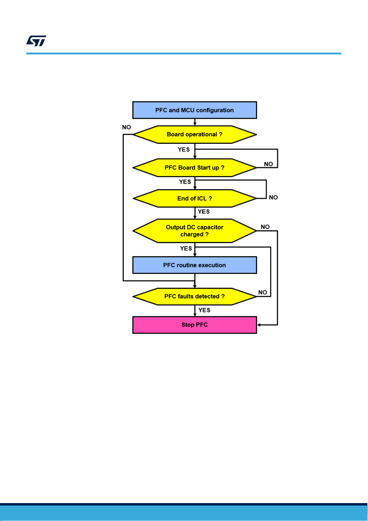
13.6 Digital PFC firmware execution
Figure 77. PFC firmware event sequence flowchart
UM2792
Digital PFC firmware execution
13.7 PFC regulation
The signal output from TIM1_CH2 and from TIM1_CH2N are used to drive power MOSFET2 and MOSFET1,
respectively. The frequency is fixed at 72 kHz and the duty cycle of the TIM1_CH2 and the TIM1_CH2N varies
according to the PFC control strategy according to the current loop computation.
UM2792 - Rev 1
page 69/101
Page 70

Figure 78. PFC management timing
UM2792
PFC regulation
TIM1_CH1 is used to start ADC1 and ADC2 as detailed in the table below. The ADC conversion starts at the end
of each TIM1_CH1 ON period. The duty cycle of TIM1_CH1 is equal to half the duty cycle of the TIM1_CH2 but
no lower than 1.5 µs to avoid invalid conversions due to noise generated by the power MOSFET switching. For
STM32 ADC the total conversion time is calculated as follows:
T
ADCconv
Sampling time + 12.5cycles
=
ADC
CLK
(91)
Table 15. ADC conversion definition
ADC Rank
ADC1_Rank1 VAC 7.5 cycles
ADC1_Rank2 IMAX 4.5 cycles
ADC1_Rank3 TEMP 4.5 cycles
ADC2_Rank1 IAC 7.5 cycles
ADC2_Rank2 HVDC 4.5 cycles
ADC2_Rank4 IAC_OFFSET 4.5 cycles
Signal measured Sampling time
UM2792 - Rev 1
page 70/101
Page 71

DMA Start
New Duty
cycle
DMA End
Start
Start
DMA End
DMA1 CH1 to start
DMA End
DMA End
DMA Start
DMA Start
DMA Start
ZVS
management
DMA Start
part
PLL first
Execution ZVS routines
HVDC
Check
HVDC Check
New Duty
cycle
PLL second
part
New Duty
cycle
New Duty
cycle
New Duty
cycle
Current loop routines
DMA End
Start
Start
Start
PFC synchronization with the AC line zero crossing
Figure 79. PFC regulation and ZVS management timing
DMA_CH1 interruption calls current loop, feed forward and PLL routines.
UM2792
Figure 80. Current loop and PLL execution flowchart
Table 16. Routine execution frequency
Routine name
Current Loop PFC regulation 72 KHz
Feed Forward PFC regulation 72 kHz
PLL_FIRST_PART routine calculation PLL calculation first part 18 kHz
PLL_SEC_PART routine calculation PLL calculation second part 18 KHz
ZVS_MANGEMENT routine Phase management and ZVS detection 18 KHz
HVDC Overvoltage Check Check HVDC Overvoltage 18 KHz
Routine definition Execution frequency
13.8 PFC synchronization with the AC line zero crossing
UM2792 - Rev 1
The PFC totem pole requires synchronization with the grid. To capture the phase information of single-phase
power grids, a single-phase phase-locked loop (PLL) method is applied.
page 71/101
Page 72

UM2792
PFC synchronization with the AC line zero crossing
Thanks to the phase information from the PLL routine (PLL_Theta) information, ZVS_Management routine is
called every 18 kHz and used to:
• manage the PFC, the voltage loop regulation at each AC line zero cross (twice the AC line frequency) and
the AC line voltage dips
• control SCRs and SiC MOSFETS according the AC line voltage polarity
• switch SCRs and SiC MOSFETs off at each AC line zero cross
• check PFC totem pole board temperature
Figure 81. PFC synchronization with the AC line zero crossing
In the figure below:
• the dotted line with number 1 indicates:
– SCRs turn off
– MOSFETs turn off
– Voltage loop communication routine
– Dip VAC detection routine
– Heat-sink overtemperature check routine
– PFC output power protection management routine
– Test HVDC: if overvoltage is detected, SCRs and MOSFETs turn off on the next half AC line cycle
• the dotted line with number 2 indicates:
– ZVS flag has been set (zero cross AC line voltage detected)
– VAC polarity has been saved
– SCRs and MOSFETs are controlled if no HVDC overvoltage is detected
UM2792 - Rev 1
page 72/101
Page 73

Figure 82. PFC management at the AC line zero crossing
MOSFET2
SCR1
SCR2
VAC
2
UM2792
PFC main files
13.9 PFC main files
The software for the digital PFC is composed of several files which contain all functions needed for the PFC
operation. The main.h file contains the definitions of the system parameters. Assuming that the host application
has the minimum necessary resources available (in terms of embedded peripherals, CPU load and code
memory), it is sufficient to include these two files in the host application firmware and to appropriately call a
function that initializes and starts the digital PFC.
13.9.1 ICL.c file
These routines manage the inrush current control at the board start up.
Get_Max_Inrush_Current_o
rder () routine
ICL_Init () routine Initializes the timer used to reduce the SCR turn-on delay from half-cycle to half-cycle of the AC
ICL_Management () routine Manages the inrush current limiter at board startup and checks whether the output DC
13.9.2 PI_Controller.c file
These routines manage the PFC.
PI_Regulator_IAC () routine PI controller implementation to shape the IAC line current on the AC line voltage
PI_Regulator_VDC ()
routine
CalcDutyFeedForward ()
routine
SET_KP_HVDC () routine Sets the proportional gain of the HVDC PI controller
SET_KI_HVDC () routine Sets the integral gain of the HVDC PI controller
SET_KP_IAC () routine Sets the proportional gain of the IAC PI controller
SET_KI_IAC () routine Sets the integral gain of the IAC PI controller
SET_KP_PLL () routine Sets the proportional gain of the PLL PI controller
Reads the value of the external potentiometer (R30) to define the step value of the constant
progressive phase control to control SCRs and therefore to control the peak inrush current.
line cycle and read SW2 ICL PEAK switch state. The step of SCR turn-on delay reduction can
be constant or variable (defined in the look up table) from one half-cycle to the following one
according to SW2 switch.
capacitor is charged
PI controller implementation to manage the PFC HVDC output voltage
To alleviate the feedback controller, a digital feed-forward control has been included in the
current loop to calculate duty ratio
UM2792 - Rev 1
page 73/101
Page 74

UM2792
PFC main files
SET_KI_PLL () routine Sets the integral gain of the PLL PI controller
RST_uDigitalLowPassFilter
() routine
Sin_Wave_Reference ()
routine
Soft_Duty_Cycle () routine Manages the duty cycle at each AC line zero crossing to reduce the IAC current spike. SiC
Soft_Start_PFC_Manageme
nt () routine
PFC_PI_Init_All () routine Initializes HVDC, PLL and IAC PI controllers
PFC_PI_Init_REG () routine Initializes HVDC and IAC PI controllers
13.9.3 PLL.c file
PLL_Zero_crossing_First_
Part () routine
PLL_Zero_crossing_Secon
d_Part () routine
Digital_LF () routine Digital low pass Filter
uDigitalLowPassFilter ()
routine
Components
DPSM_Trig_Functions ()
routine
Park_Transformation ()
routine
Rev_Park_Beta () routine Reverses Park transform
Calc_Sin_Value_Ref ()
routine
ShiftElectricAngle ()
routine
PI_Regulator_PLL ()
routine
Resets digital low pass filter
Generates the AC line current sine wave reference
MOSFETs are controlled with a small pulse width. The pulse gradually increases to normal duty
cycle
During the board power-up, the internal voltage loop output increases from initial voltage under
soft-start, reducing the current stress for all power switches. Once HVDC has reached 400 VDC,
the soft-start control is released to achieve regulation.
Tracks the frequency and phase of the AC line voltage (first part)
Tracks the frequency and phase of the AC line voltage (second part)
Digital low pass Filter
Define cos and sin values according to the angle value
Park transform
Defines sin value
Shifts the phase angle of the current signal reference from the AC line voltage
PI controller implementation to manage the PLL
13.9.4 System.c file
AC_Line_RMS_Detection () RMS and Peak AC line voltage measurement
AC_Line_Freq_Detection ()
routine
Init_Switch_OFF_PFC ()
routine
Get_Temp () routine Heat-sink temperature measurement
Get_Main_Voltage ()
routine
Get_Main_Voltage_Rectifie
r () routine
Get_IAC_Current_uint32 ()
routine
UM2792 - Rev 1
AC line frequency measurement
Switches PFC off and initializes MCU parameters
AC line voltage measurement
Absolute value of the AC line voltage measurement
PFC chock current inductor measurement
page 74/101
Page 75

UM2792
PFC main files
Get_REF_IAC_Sensor_uint
Reference voltage of the current sensor measurement
32 () routine
Get_HVDC_output ()
PFC HVDC output voltage measurement
routine
Board_Operational ()
Flashing LEDs indicating the board is operational
routine
CLEAR_IT_DMA_TC ()
Clears IRQ DMA
routine
PVD_Config () routine PVD configuration
Check_Board_StartUp ()
Checks AC line frequency, AC line RMS voltage, heat-sink temperature and current sensor
routine
Init_MCU () routine Initializes all MCU parameters
PFC_TIMING_Management
() routine
Manages the zero crossing of the AC line voltage, the AC line drops and the heat-sink
temperature
13.9.5 PFC_FAULT_DETECTION.c file
PFC_BusVoltageCheck ()
routine
PFC_OutputPowerProtecti
on () routine
PFC_OverCurrent_Check ()
routine
PFC_IAC_Sensor_Check ()
routine
PFC_OverTemp_Check ()
routine
Dips_VAC_Detection ()
routine
PFC_Statut_Led_Managem
ent () routine
PFC_Statut_Faults_Manag
ement () routine
Checks PFC output HVDC voltage
Checks the PFC output power
Checks the PFC chock inductor overcurrent
Checks the current sensor
Checks the heat-sink temperature
Detects the AC line drops
Manages LED state
Manages PFC fault detection
UM2792 - Rev 1
page 75/101
Page 76

51
PC11
A_GND
C23
33
PB13
34
I/O 2
3
A_GND
C26
ADC12_IN6
TP36
R16
+3.3V
8
PB12
COMP2_OUT/HRTIM_FLT1
TIM2_ETR
3
22pF
R25
10
ADC1_IN2
C19
Green LED
100pF
GND
10
STATUS_LED
A_GND
C8
FAULT_LED
PWM_1
I2C1_SDA/USART3_TX/CAN_TX
+3.3V
TP31
C32
L1
ADC2_IN5
HRTIM_CHC2
PWM_5
I2C1_SDA/USART3_TX/CAN_TX
ADC1_IN1
NRST
100nF
C10100nF
8
VBAT
12
+5V
TP3
Jumper
TP29
To pull-up when used for SMBUS communication
PC13
COMP6_OUT/TIM3_CH1/TIM1_CH3N/HRTIM_EEV10
+5V
1
DAC1_OUT1/SPI1_NSS
DAC2_OUT1
TP19
COMP4_INP/ADC1_IN11/OPAMP2_VINP
PB3
55
PWM_12
PA9
HRTIM_EEV1
HRTIM_CHE1
C33
PF0/OSC-IN
6
+5V
PA0
TP35
A_GND
PB1
7
100nF
7
X1
3
VIN
PC13
HRTIM_EEV7/SPI1_MISO
HRTIM_CHB1
1
24
PC5
5
VSS_
63
100uF
R31
PB7
59
10
ADC1_IN3
GND
53
PD2
100pF
I/O 4
6
REF3
REF4
8
37
PC7
38
1
10nF
+3.3V
5
REF4
3
GND
9
I/O 2
3
J4
HRTIM_CHE2
DAC1_OUT2/SPI1_SCLK
COMP_1_INP/ADC_11
TP21
R17
I/O 3
4
HRTIM_CHD2
10
ADC2_IN11/OPAMP2_VINM
HRTIM_CHC2
1.5 Ohm 215 mA
C31
2
ADC2_IN5
PWM_8
SMBus_SDA/UI_USART_TX
CAN_RX
REF2
TP22
J5
46
VDD_2
32
100nF
Digital Power Connector pinout assignment for STM32F334R8T6 MCU
ADC_4/DIFF_ADC_2-/OP-AMP_2-
GND
PA14
3
100nF
U3
HRTIM_CHB2
100pF
R27
10
HRTIM_FLT5
A_GND
PA7
23
7
PF1/OSC-OUT
NRST
TP17
R36
PB14
PC10
100uF
100pF
COMP6_INP
C9
I/O 3
4
R200
100nF
TP34
I/O 2
3
VSS_4
COMP2_OUT/HRTIM_FLT1
TP5
0
R37
ADC1_IN2
C12
Red LED
R29
C20
COMP_2_INP/ADC_12/OP-AMP_1+
ADC_8
GND
52
PC12
100pF
R35
ADC1_IN1
Blue LED
I2C1_SDA/USART3_TX/CAN_TX
USART1_RX
GND
R210
C29
1
TP9
R30
10
100nF
HRTIM_CHD1
PWM_4
TIM2_CH3
100pF
GND
ADC12_IN6
TP7
7
VSSA/VREF-
VSS_2
ANALOG INPUT FILTERS
VOLTAGE REGULATOR
U5
TP8
GPIO_5/DAC_1/COMP_4_INP/SPI_NSS
ADC12_IN7
PB9
62
100pF
42
PA10
43
PWM_11
GND
+3.3V
1
PC2
+3.3V
15
STM32F334R8T6 (LQFP64)
PA2
2
1
50
PB0
VDDA
C30
100nF
J6
10K
REF3
7
HRTIM_EEV7/SPI1_MISO
HRTIM_CHB2
PB4
56
PC6
8
PC0
GPIO_2/COMP_2_OUT/GP_PWM_2
A_GND
100pF
TP13
R28
10
57
PB6
58
39
PC9
40
VDDA
ADC2_IN11/OPAMP2_VINM
2
470nF
2
DA2
8MHz HC49/US
PWM_2
A_GND
22pF
10
DA108S1
TP2
D3
I/O 1
2
10 HRTIM Outputs on STM32F334
TP11
5
A_GND
29
PB11
30
USART1_TX
PC14/OSC32_IN
4
C28
ADC_6/OP-AMP_1-
GND
J7
10uFC16
1
HRTIM_CHD1
PWM_7
SMBus_SMBA/SPI_MOSI
I2C1_SCL/USART3_RX/CAN_RX
TP27
U4
TP1
TP18
ADC12_IN8
8
GND CON
Stripline male 2x1 2.54mm
PA11
44
VDDA/VREF+
+5V
31
2
HRTIM_CHA1
GPIO_1/COMP_3_OUT/GP_PWM_1/EEV_4
I2C1_SMBA/SPI1_MOSI
VDDA
GND
GND
A_GND
35
PB15
36
REF1
1
+
PC1
9
+3.3V
GPIO_6/DAC_2/SPI_SCLK
GPIO_7/DAC_3/OP-AMP_1_OUT
GPIO_8/EEV_2
GPIO_9/EEV_3/SPI_MISO
GPIO_10/DAC_4
1
2
A_GND
HRTIM_EEV2
I/O 1
2
VDD_419PC4
PA13
NRST
1
HRTIM_CHE2
ADC1_IN3
TP32
ADC_7/COMP_2_INM
ADC_9
TP37
5
REF4
+3.3V
DA108S1
+3.3V
C24
100pF
TP20
GND
C5
COMP2_INP/ADC2_IN4
TP16
R15
COMP4_OUT/TIM3_CH4
HRTIM_EEV1
TP25
COMP6_OUT/TIM3_CH1/TIM1_CH3N/HRTIM_EEV10
I2C1_SCL/USART3_RX/CAN_RX
HRTIM_FLT5
ADC_1/DIFF_ADC_1+
ADC_2/DIFF_ADC_1-/OP-AMP_2+
ADC_3/DIFF_ADC_2+/OP-AMP_2_OUT/COMP_1_NM
C17
100
ADC12_IN7
+3.3V
48
VDD_3
4.7k
BOOT0
60
+
17
PA4
VDDA
ADC12_IN8
ADC1_IN4
MCU_USART_RX
PWM_10
DAC1_OUT2/SPI1_SCLK
2
C14
2
GND
2
10
PC3
11
COMP2_INP/ADC2_IN4
HRTIM_EEV2
FAULT_LED
I/O 4
6
HRTIM_CHC1
PB5
Note: Keep ADC traces as short as
possible to connector P1
GND
SWD - USER COMMUNICATION
COMP_3_INP
2
PC13
I2C1_SMBA
PWM_3
VDDA
C25
1
PB8
61
TP28
R23
TIM3_ETR
PC8
DA108S1
EXT SUPPLY
R32
C7
C15
R19
TP23
OSC-IN
HRTIM_SCOUT
DAC1_OUT1/SPI1_NSS
REF1
1
HRTIM_CHE1
6
100pF
C21
I2C1_SCL/USART3_RX/CAN_RX
ADC_10
ADC1_IN4
VDDA
MCU_USART_TX
100nF
R34
10
REF2
PWM_6
I2C1_SDA/USART3_TX/CAN_TX
TP26
R26
10
TP30
TP4
SWCLK
ADC2_IN12
7
REF1
1
R33
10
LD1117
1
GND
VSS_3
47
4th DAC channel not available
BAR43S
+3.3V
A_VDD
I2C1_SMBA/SPI1_MOSI
HRTIM_CHA1
A_GND
STATUS_LED
GND
COMP6_INP
SMBus_SCL/UI_USART_RX
20
PA5
1
COMP4_OUT/TIM3_CH4
2
COMP4_INP/ADC1_IN11/OPAMP2_VIN
2
P
6
PB10
PC15/OSC32_OUT
5
VDDA
14
PA1
TP12
DA3
+
C11
I/O 1
2
PB2
28
J3
REF2
GND
2
VOUT
TP14
I/O 3
4
2
HRTIM_CHA2
TP6
10
PA12
45
TP10
TP15
R24
10
13
GND
TP24
DA1
5
54
4.7k
4
GND
USART1_TX
2
0
R18
D2
C6
SWDIO
C22
100pF
HRTIM_CHC1
10
ADC2_IN12
HRTIM_CHD2
DAC2_OUT1 USART1_RX
100pF
C27
SWCLK
C13
86
I/O 4
6
REF3
2
SWD/COM
16
GND
C18
PA3
CAN_TX
SWDIO
OSC-OUT
PA8
41
ADC_5
PWM_9
I2C1_SCL/USART3_RX/CAN_RX
TP33
+3.3V
18
100pF
R22
10
GND
49
PA15
HRTIM_CHB1
D1
A_GND
FAULT_1
GPIO_3/COMP_1_OUT/FAULT_2
GPIO_4/EEV_1
1
1VDD_
64
PA6
22
HRTIM_CHA2
1
GND
UM2792 - Rev 1
14 Schematic diagrams
Figure 83. STEVAL-DPS334M1 circuit schematic (1 of 3)
page 76/101
Schematic diagrams
UM2792
Page 77

+3.3V
+3.3V_iso
USART_TX_iso
+5V
PWM_11
GPIO_2/COMP_2_OUT/GP_PWM_2
A_VDD
FAULT_1
PWM_1
CAN_TX
SMBus_SCL/UI_USART_RX
SMBus_SDA/UI_USART_TX
PWM_2
PWM_4
PWM_6
PWM_8
CAN_RX
PWM_3
PWM_5
PWM_7
PWM_9
SMBus_SMBA/SPI_MOSI
GPIO_4/EEV_1
GPIO_5/DAC_1/COMP_4_INP/SPI_NSS
GPIO_7/DAC_3/OP-AMP_1_OUT
GPIO_9/EEV_3/SPI_MISO
ADC_1/DIFF_ADC_1+
COMP_1_INP/ADC_11
COMP_3_INP
USART_RX_iso
ADC_2/DIFF_ADC_1-/OP-AMP_2+
ADC_3/DIFF_ADC_2+/OP-AMP_2_OUT/COMP_1_NM
PWM_10
PWM_12
GPIO_3/COMP_1_OUT/FAULT_2
ADC_7/COMP_2_INM
ADC_4/DIFF_ADC_2-/OP-AMP_2-
ADC_5
ADC_6/OP-AMP_1-
COMP_2_INP/ADC_12/OP-AMP_1+
ADC_8
ADC_9
ADC_10
GPIO_6/DAC_2/SPI_SCLK
GPIO_8/EEV_2
GPIO_10/DAC_4
A_GND
GND_iso
GPIO_1/COMP_3_OUT/GP_PWM_1/EEV_4
GND
GND
P1
1B
1B
2A
2A
2B
Digital Power Connector
2B
3B
3B
4A
4A
4B
4B
5A
5A
5B
5B
6A
6A
6B
6B
7B
7B
8A
8A
8B
8B
9A
9A
9B
9B
10A
10A
10B
10B
11A
11A
11B
11B
12A
12A
12B
12B
13A
13A
13B
13B
14A
14A
14B
14B
15A
15A
15B
15B
16A
16A
16B
16B
17A
17A
17B
17B
18A
18A
18B
18B
19A
19A
19B
19B
20A
20A
20B
20B
21A
21A
21B
21B
22A
22A
22B
22B
23A
23A
23B
23B
24A
24A
24B
24B
25A
25A
25B
25B
7A
7A
1A
1A
26B
26B
29B
29B
27B
27B
28B
28B
30B
30B
26A
26A
27A
27A
28A
28A
29A
29A
30A
30A
32A
32A
31B
31B
32B
32B
31A
31A
3A
3A
UM2792 - Rev 1
Figure 84. STEVAL-DPS334M1 circuit schematic (2 of 3)
page 77/101
Schematic diagrams
UM2792
Page 78

TO PLACE ON THE RIGHT AND ON THE LEFT SIDE OF THE BOARD RESPECTIVELY
0 N.M.
47 R11
R13
U2
15pF
7
5
USART_TX_iso
USART_RX_iso
GND_iso
GND
GND
0 N.M.
R6
SHIELD
GND
USART_TX_iso
R10 820
J1
J2
MCU_USART_RX
1
USART_TX_iso
39
PS9821
MCU_USART_TX
+3.3V
4
R12
GND_iso
GND_iso
8
+3.3V_iso
+3.3V_iso
0 N.M
GND
8
0 N.M
R4
47
+3.3V_iso
1
2
3
4
OPTOCOUPLERS
CONNECTION BETWEEN TWO CONTROL BOARDS
USART_CON
6
U1
7
USART_CON
MCU_USART_TX
3
2
SHIELD
63
USART_RX_iso
1
2
3
4
5
USART_RX_iso
C1
R14
15pF
R3
0
R7
GND_iso
PS9821
GND
GND_iso
39 R9
100nF
0
R5
C3
0
820 R2
GND_iso
+3.3V
USART_TX_iso
USART_RX_iso
GND
1
C4
R8
+3.3V
MCU_USART_RX
100nF
R1
0
MCU_USART_TX
2
4
+3.3V_iso
C2
UM2792 - Rev 1
Figure 85. STEVAL-DPS334M1 circuit schematic (3 of 3)
page 78/101
Schematic diagrams
UM2792
Page 79

2
P1
Male Connector 2x10
Pitch 2.54 mm
TD
RD
J10 as close as possible to j12 pin 10
JTDI_JTAG_ADP
JTMS_ADP
10k
5
NC1
T1IN
7
J9
4
RESET#_BTN
GND
J1
100nF 25V
GND
SG
DB9-Female
7
Jtag conn.
R3
100nF 25V
4
V+
2
11
GND
USART_RX
CAN_RX
100nF
J3
1
11
RESET#_BTN
1
GND
4
T1OUT
14
1
6
2
7
3
8
4
9
5
I2C_SCL/USART_RX/CAN_RX
2
SWD - JTAG USER COMMUNICATION
RESET BUTTON
1
3
S1
RST
+3.3V
C2-
5
GND
GND
5
11
13
GND
JTMS_ADP
+3.3V
2
4
6
8
1
JP_JTDI
RESET#_ADP
SMBUS_SDA
T2IN
10
120
100nF 25V
C4
CAN_TX
I2C_SDA/USART_TX/CAN_TX
7
CANH
3
GND
C2+
4
C2
2x stripline male 3+1 2.54mm
pin 4 can be connected with pin 1, 2 or 3 with a jumper
+3.3V
3
2
1
3
5
7
9
D
1
+3.3V
JTCK_ADP
J7
4.7k
C8
CAN_RX
0
USART_TX
R1
DB9-Male
14
16
20
R2
P2
9
10
I2C_SMBA
R5
0
I2C_SMBA
R6
19
U2
I2C_SCL/USART_RX/CAN_RX
5
GND
U1
R2OUT
C+
1
RESET#_ADP
NC
8
18
SWD/COM
J8
2
C5
+3.3V
8
SMBUS_SDA
I2C_SDA/USART_TX/CAN_TX
8
R2IN
USART_TX
10
+3.3V
place reset button in the external part of the board
C7
JTCK_ADP
USART_RX
R1IN
13
SMBUS_SCL
+3.3V
C6
1
6
2
7
3
8
4
9
5
GND
3
C1-
12
R1OUT
1
T2OUT
VCC
16
R
4
6
CAN_TX
9
GND
3
15
100nF 16V
USER COMMUNICATION CONFIG
Stripline male 3x2 2.54mm
+3.3V
17
SMBUS
RS:461-9771
JTDO_ADP
GND
2
ST3232CTR
1
SMBUS_SCL
J2
J6
100nF 25V
SN65HVD232D
1
GND
15
12
VCC
3
V-
6
RS-232
CAN
6
4
GND
GND
100nF 25V
C3
C1
R4
100nF 25V
GND
SERIAL COMMUNICATION
CAN COMMUNICATION
GND
N.M.
6
CANL
2
4.7k
2
+3.3V
UM2792 - Rev 1
Figure 86. STEVAL-DPSADP01 circuit schematic
page 79/101
Schematic diagrams
UM2792
Page 80

16B
48
SCR2
12
12B
59
28B
60
PC8
42
11A
11
19B
1
TX_PC
3
300R
R6
PC6PC7
300R
R5
2
IAC_SENSE_Filtered
THETA
4A
4
PB7
LED4
3
A_GND
GND
C5
3
PB11
PA12
5V_DC
16A
16
30B
PA6
PB1
PB14
61
27B
VAC_SENSE
SCR1
A green
LED1
40
9A
9
J1
43
12A
A_GND
PC0
5V
LED2_STATUS
2
LED8_STATUS
LED6_STATUS
FAN_CTRL
A_GND
A green
55
24A
24
LED3
3B
35
TEMP
A_GND
1 Led_bicolor
R9
LED1_STATUS
300R
R10
38
7B
39
300R
PC1
31B
P1
A_GND
300R
29B
C
C
A green
A red
A red
17A
17
A red
GND_DC
LED2
ZVS
IAC_SENSE_Filtered
R98
C7
A green
PB15
A red
8A
8
LED9_STATUS
GND_DC
PC13
conn_5_pts
3
MOS2
LED2_STATUS
54
23A
23
2
300R
PA8
5A
5
300R
10R
PB0
63
32B
4.7uF
44
13A
CAN_TX
17B
49
25B
57
14A
DC/DC_START
2
C
A_GND
PFC_START
5V_DC
51
20A
20
C
2
LED6
MOS1
1 Led_bicolor
R12
10R
3V3_DC
21
21B
53
1A
1
LED6_STATUS
3V3_ISO
GND
10A
10
PA1
R11
23B
10nF
3V3_DC
3V3
64
31A
31
LED5_STATUS
R97
100pF
11B
PA9
PA11
14B
7A
7
PA3
C6
PB12
20B
52
R1
5
C2
GND_DC
300R
PA10
A_GND
1B
33
PA4
10B
PB6
A_VDD
LED3_STATUS
GND_DC
PA2
HV_DISCHARGE
GND_DC
1uF
28A
8B
PC5
A_GND
DC/DC_START
13
13B
45
R4
C1
6B
PB13
5B
24B
56
14
A_GND
300R
A_GND
LED5_STATUS
GND_DC
4
1 Led_bicolor
3A
3
CAN_RX
LED10_STATUS
R13
PB2
2B
R7
18A
PB4
100pF
12V_DC
A_GND
1 Led_bicolor
PC4
C
26
27A
27
26B
58
A_GND
19A
19
300R
PC9
37
6A
6
2
30
32A
32
21A
GND_DC
LED8_STATUS
R2
PC11
3
28
29A
IAC_SENSE
IMAX
2A
2
29
30A
LED7_STATUS
46
15A
15
1 Led_bicolor
Digital Power Connector
LED4_STATUS
LED3_STATUS
PB5
22B
LED10_STATUS
EXTERNAL CONNECTORS
LED STATUS
100pF
C3
PA5
I_AC
HVDC
R3
4B
36
HVDC_SENSE
LED5
A_GND
GND_ISO
9B
41
A green
3
PC12
A red
A_GND
LED1_STATUS
GND_DC
PA0
LED7_STATUS
GND_DC
A_GND
62
26A
10R
C4
300R
LED4_STATUS
RX_PC
FIX_VAR
34
22A
22
PC2
15B
47
LED9_STATUS
GND_DC
10R
A_GND
R8
25A
25
18
18B
50
100pF
Freq
V_AC
Temp
UM2792 - Rev 1
Figure 87. STEVAL-DPSTPFC0 circuit schematic (1 of 4)
page 80/101
Schematic diagrams
UM2792
Page 81

24R
1nF
C41
2
Vcc-
8
3
In-
Q2
100nF
U3
6
OUT
5V_SCR1
R15
39K
SW1
100nF
R45
1k
C58
1uF
C21
R44
2
C42
1
3V3_DC
R59
GND_SCR1
150pF
R17
390R
A_GND
R55
GND
2
LM35/TO220
2
SPDT PCB slide switch
HVDC_SENSE
A_GND
U8
270R
270R
D2
1uF
C22
C137
NC
GND_S2
VH
5
160k
C59
GND_DC
A_GND
100nF
U4
+
-
10k
10k
40k
D3
NC
4.7uF
C24
GON
6
470k
R47
10k
2N2907A
R52
C39
10
9
OUT2
C31
2
IN+
R58
STGAP2SM
68nF
1.3k
8
1
L16
2A
3V3_DC
470k
GND_SCR1
A_GND
NC
C11
150pF
R37
C40
C52
R42
A_GND
NC
A_GND
160k
3k
C14
2
TEMP
A_GND
FAN_CTRL
IMAX
D6
NC
4 1
Q1
GON
6
GND_S2
24R
40k
K
2
1k
2A
NCC135
R18
R40
U2
8
1nF
R22
GND_S2
470k
-
2
K
2
C10
C49
12
GND
TP1
2
3V3_A
MCP6231UT-E/OT
C50
10nF
3
150pF
G_SCR2
R43
A_GND
STTH1L06A
10nF
3
150pF
C19
C30
470k
STN4NF03L
R34
L15
D4
R23
1
VDD
MOS1
3V3_DC
NC
C134
IAC_OFFSET
GND_DC
U6
GND_DC
4.7uF
R24
5R
1uF
160k
3
IN-
C18
C35
C26
R41
NC
2.2nF
3V3_DC
IN1
1
C44
10nF
R56
2N2907A
390R
5
OUT3
10k
GND_DC
A_GND
2
GND_DC
U24
-3V_S2
U1
GND_DC
R38
75R
1
1
0.55K_W
100nF
10k
1uF
R54
100R
4.7uF
L1
NC
GND_DC
470k
R100NC
IM2
GND_DC
C36
150pF
R46
C20
100nF
R48
VAC sensor
MAX INRUSH CURRENT ORDER
ON/OFF PFC
Temperature sensor
IAC sensor
HVDC sensor
ICL FIX/VAR
Fan control
SWITCHES CONTROL
ZVS detection (optional)
C53
LTV-817
SPDT PCB slide switch
G_MOS1
3
IN-
5V_SCR2
GND_S1
C139NC
A
1
10k
NC
24R
L1
1
In+
510R
R26
10k
IN3
3
R21
G_MOS2
VAC_SENSE
3V3_A
4.7uF
COM
3
C51
R39
V+
7
13
VC
14
3
C37
470k
Q3
47R
10nF
R53
1k
VAC_SENSE
R57
C9
Vcc+
Out
4
C8
5V_A
GND_ISO
G_SCR1
2.2nF
C28
GND_DC
C12
NC
N1
C15
10nF
C13
10nF
1uF
4
GND
3V3_DC
MOS2
IAC_SENSE
A_GND
3.9nF
C43
C38
R14
4
A_GND
VREF
11
1
1
R32
VH
5
C27
1uF
39K
150pF
GND_S1
-
20V_S1
U28
HVDC
R99NC
R27
C23
390R
R29
GND_ISO
R30
7
GOFF
NCR101
3V3_A
470k
R25
1k
20V_S2
V-
4
SCR1
C25
1
U5
LTV-817
D5
PFC_START
R49
C29
GND_SCR2
GND_DC
U7
C46
C57
IM1
150pF
C60
NC
R36
R35
5k
VS
1
C45
100R
VDD
1
GND_DC
GND_SCR2
NC
FIX_VAR
GND_S1
2A
NC
470k
680INT_REF
A_GND
R50
A
1
LEM CASR 15-NP
A_GND
3
2
IN2
7
GOFF
C34
150pF
OUT1
2
10nF
C33
R16
R33
3
OUT
470k
100nF
R31
R20
3V3_DC
SW2
MG1
SCR2
100nF
ZVS
+
3
C138NC
1uF
R19
R28
3V3_A
1uF
47R
3
COM
1uF
IN+
STGAP2SM
12V_DC
100nF
4
GND
A_GND
390R
24R
68nF
5V_A
1
R51
VOUT
510R
C56
3V_S1
10k
Rm
UM2792 - Rev 1
page 81/101
Figure 88. STEVAL-DPSTPFC0 circuit schematic (2 of 4)
Schematic diagrams
UM2792
Page 82

L14
C66
R79
N1
33nF
J8
STN4NF03L
IM1
C78
10k
DZ1
NC
NEUTRAL1
GND_S2
1
1
C54
R73
self_boost_WE
1M5
C82
Y24.7nF
S14K250/EPC
33nF
C71
C80
GND_DC
L1
3.3 uF
Q5
DC-
1
1
R106
R76
LED7
J6
0R_10A
165k
JP2
GND_DC
R70
4
C73
NC
33k 5W
S14K385/EPC
C61
NC
Q4
4.7nF Y2
S14K250/EPC
L4
1
1
LINE1
X3_S
Q7
1
J
1k
R105
7
470nF
C67
R66
MMSZ5256BT1G
+
G_SCR1
HVDC
165k
15A_connector
R74
NC
22nF
33nF
X1_S
+
1
D10
165k
1.6mH_16A
3
R65
C79
U
1
1M5
X4
Y2
4.7nF
R68
U
1M5
GND_SCR2
G_SCR2
X1_D
U
1
1
1
D12
1
X1_G
2
R104
NC
1M5
Y2
4.7nF
X2
15A_connector
D7
NC
U
R103
R63
SCTW35N65G2V
HVDC SECURITY
cap discharge + visualisation
680uF/450V
1
1
3.3k
TS756
Y2
4.7nF
JP1
C74
P6KE440A
2
4
G_MOS2
C81
165k
1M5
1
X3
LINE
Y2
4.7nF
165k
+
BUL216
C75
J3
L18
DC+
1
X3_G
1
165k
SIOV1
C76
30A_connector
R81
30A_connector
R64
R80
C127
22nF
NEUTRAL
30A_connector
GND_SCR1
C63
C68
R77
NC
1
C70
NC
1
1
C77
SIOV4
C65
D8
0R_10A
2mH_10A
1
MMSZ5245BT1G
U
1
470nF
SIOV3
C64
D11
C62
1M5
680uF/450V
4
Q6
HVDC
1.6mH_16A
3
1
1
IM2
220nF
R61
TN3050H-12WY
SIOV2S14K385/EPC
JP3
1.6mH_16A
3
HV_DISCHARGE
R62
R69
TN3050H-12WY
GT1
2
L3
33nF
L10
SCTW35N65G2V
0R_10A
STQ1NK80ZR-AP
X3_D
C72
NC
5V_DC
MMSZ5V6T3G
J5
1M5
1M5
R67
680uF/450V
C32
1M5
SIOV5
GND_S1
F1
STN4NF03L
G_MOS1
2
R60
C69
S14K385/EPC
X1
1
C55
33nF
UM2792 - Rev 1
Figure 89. STEVAL-DPSTPFC0 circuit schematic (3 of 4)
page 82/101
Schematic diagrams
UM2792
Page 83

C93
8
10nF
+VIN
10nF
10nF
3
INH
C118
5V_SCR1
220uF/63V
5
OUT
3
OUT
C133
5V_DC
+
22uF/16V
C107
GND_DC
C120
C131
NC
60R
2
L5
+
C105
33uF/25V
C88
33uF/25V
D18
C94
C117
U11
L8
D15
C95
C104
5
12V_DC
10nF
4
BYP
2
39 mH
2A
R94
U15
100nF
A_GND
C85
STTH1R06A
C130
4.7nF
Y2
20V_S2
C91
R90
1mH
10uF/450V
Y2
STPS1150A
3
C110
+
viper26LD
+
C108
T1
1nF
STTH112UFY
C48
NC
GND_DC
C126
-
-VIN
-Vout
0V
6
IN
1
100nF
R89
1.5KE400A
2
3V3_A
1
+VIN
7
MGJ2D122005SC
20V_S1
47 R / 5W
N1
DZ2W03300L
C114
10nF
C92
C125
C119
+
DRAIN
L9
100uF/16V
U13
Y2
GND_SCR1
C102
C116
+
C100
D14
100nF
4.7uF
A_GND
D17
5V_A
2
-3V_S2
1
1
C17
Y2
150pF
C97
60R
GND
12V_DC
L1
C98
SIOV6
C123
STPS1150A
IN
1
1k
U12
LIM
14D911K
1
60R
C96
L12
4.7uF
C103
12V_DC
100nF
C121
2A
LD2985BM33R
C101
DZ2
33uF/25V
U10
3.9k
10nF
4.7uF
VDD
FB
C111
6
C84
-3V_S1
C115
5
R84
100nF
-
38k3
39 mH
TL432
LTV-817
C124
100nF10nF
D19
60R
SIOV7
+
GND
2
R82
N1
N1
4
5
GND
2
10nF
2A
22uF/16V
R95
-
GND_DC
MGJ2D122005SC
C90
100nF
220uF/25V
GND_S1
C113
60R
myrra74010
D13
Y2
STPS1150A
R86
9
L11
4.7nF
22uF/25V
C99
DZ2W03300L
+
2.2uF/35V
R85
L13
C87
+
C109
D16
C106
+
1,5mF/16V
R83
-
L7
+Vout
GND_DC
10nF
N1
U9
U16
L78M05ABDT
3
OUT
GND_DC
5V_DC
60R
33uF/25V
COMP
GND_DC
4.7uF
C122
100k
10k
R87
10nF
7
R93
C128
22uF/25V
GND
2
U14
60R
C47
NC
-
100nF
100nF
L6
2A
-
5V_SCR2
7
10uF/450V
L78M05ABDT
IN
1
3
3V3_DC
GND_SCR2
3V3_DC
100nF
R88
+Vout
-VIN
-Vout
0V
6
U
C112
NC
C83
C16
Y2
22uF/16V
Y2
4.7nF
100nF
R107
S14K385/EPC
R96
60R
100nF
UM2792 - Rev 1
page 83/101
Figure 90. STEVAL-DPSTPFC0 circuit schematic (4 of 4)
Schematic diagrams
UM2792
Page 84

15 Bill of materials
Table 17. STEVAL-DPSTPFC1 bill of materials
Item Q.ty Ref. Part/Value Description Manufacturer Order code
1 1
2 1
Table 18. STEV
AL-DPS334C1
Table 21. STEV
AL-DPSTPFC0
Table 18. STEVAL-DPS334C1 bill of materials
Item Q.ty Ref. Part/Value Description Manufacturer Order code
1 1
2 1
Table 19. STEV
AL-DPS334M1
Table 20. STEV
AL-DPSADP01
Digital power
control board
PFC bridge-less
totem pole
Digital power
control module
DSMPS adapter ST Not available for separate sale
ST Not available for separate sale
ST Not available for separate sale
ST Not available for separate sale
UM2792
Bill of materials
Table 19. STEVAL-DPS334M1 bill of materials
Item Q.ty Ref. Part/value Description Manufacturer Order code
1 2 C1, C4 15 pF 25 V ±10% smc0603 XR7 Ceramic capacitor Any
C2, C3, C7,
2 11
3 2 C5, C6 22 pF 25 V ±10% smc0603 XR7 Ceramic capacitor Any
4 2 C9, C11 100 µF 16 V ±20% capAluminumC
5 1 C16 10 µF 16 V ±10% tantalioB Tantalium capacitor KEMET T491B106K010AT
6 1 C17 10 nF 25 V ±10% smc0603 XR7 Ceramic capacitor Any
7 1 C19 470 nF 25 V ±10% smc0603 XR7 Ceramic capacitor Any
8 13
9 3
10 1 D1 1.9 V smd0603 Green LED KINGBRIGTH KP-1608CGCK
11 1 D2 1.9 V smd0603 Blue LED KINGBRIGTH KP-1608QBC-D
12 1 D3 1.9 V smd0603 Red LED KINGBRIGTH KP-1608 SRC-PRV
13 2 J1, J2 USART_CON COn4TE215079
14 1 J3 EXT SUPPLY MOR2X254 Terminal block Phoenix Contact 1725656
15 3 J4, J5, J6 CON2A SIPTM2002
C8, C10,
C12, C13,
C14, C15,
C18, C33
C20, C21,
C22, C23,
C24, C25,
C26, C27,
C28, C29,
C30, C31,
C32
DA1, DA2,
DA3
100 nF 25 V ±10% smc0603 XR7 Ceramic capacitor Any
Electrolytic
capacitor
100 pF 25 V ±10% smc0603 XR7 Ceramic capacitor Any
DA108S1 sog0508wg244l200 Diode array ST DA108S1
Ribbon cable
connector
Strip Line Male
2X1 pitch 2, 54mm
PANASONIC EEEFT1C101AR
TE Connectivity 7-215079-4
Any
UM2792 - Rev 1
page 84/101
Page 85

UM2792
Bill of materials
Item Q.ty Ref. Part/value Description Manufacturer Order code
16 1 J7 SWD/COM AMPMODE10 Connector header HARTING 9185106324
17 1 L1 470 Ohm 100 MHz 250 mA sml0402 Ferrite beads
18 1 P1 64 pin Conn64X254Harting09021646921
19 5
20 2 R2, R10 820 1/16 W ±1% smr0603 SMD Thick film resistor Any
21 2 R3, R9 39 1/16 W ±1% smr0603 SMD Thick film resistor Any
22 2 R4, R11 47 1/16 W ±1% smr0603 SMD Thick film resistor Any
23 2 R5, R7 0 750 mW ±5% SMR2010 SMD Thick film resistor VISHAY CRCW20100000ZOEF
24 0 R6, R8 750 mW ±5% SMR2010 SMD
25 0 R13, R14 750 mW ±5% SMR2010 SMD
26 1 R15 100 1/16 W ±1% smr0603 SMD Thick film resistor Any
27 14
28 1 R17 86.6 1/16 W ±1% smr0603 SMD Thick film resistor Any
29 1 R18 0 1/4 W ±1% smr1206 SMD Thick film resistor Any
30 1 R19 10 K 1/16 W ±1% smr0603 SMD Thick film resistor Any
31 2 R35, R36 4.7 k 1/16 W ±1% smr0603 SMD Thick film resistor Any
32 37
33 2 U1, U2 PS9821 sog0508wg244l200
34 1 U3 LD1117 800 mA ±1% SMDPACK
R1, R12,
R20, R21,
R37
R16, R22,
R23, R24,
R25, R26,
R27, R28,
R29, R30,
R31, R32,
R33, R34
TP1, TP2,
TP3, TP4,
TP5, TP6,
TP7, TP8,
TP9, TP10,
TP11, TP12,
TP13, TP14,
TP15, TP16,
TP17, TP18,
TP19, TP20,
TP21, TP22,
TP23, TP24,
TP25, TP26,
TP27, TP28,
TP29, TP30,
TP31, TP32,
TP33, TP34,
TP35, TP36,
TP37
0 1/16 W ±1% smr0603 SMD Thick film resistor Any
10 1/16 W ±1% smr0603 SMD Thick film resistor Any
Male DIN 41612
through hole
Thick film resistor
(not mounted)
Thick film resistor
(not mounted)
Test point Any
Optocoupler 1
chanel
Adjustable and
fixed low drop
positive voltage
regulator
WURTH
ELEKTRONIK
Erni 533406
Any
Any
NEC PS9821-1-F3-AX
ST LD1117DT33TR
7427927141
UM2792 - Rev 1
page 85/101
Page 86

UM2792
Bill of materials
Item Q.ty Ref. Part/value Description Manufacturer Order code
35 1 U4
36 1 U5 BAR43S 30 V, 0.1 A smsot23123
37 1 X1 8 MHz HC49/US Crystal oscillator EUROQUARTZ
37 1 2.54 mm Flat cable Samtec Inc.
38 1 Micro-Match 4 ways, 9.9"", 250mm, 1.27mm AMP Micro-MaTch TE Connectivity 1483350-3
STM32F334R8T6 (LQFP64)
quad50m64wg1200
Table 20. STEVAL-DPSADP01 bill of materials
Item Q.ty Ref. Part Description Manufacturer Order code
1 8
2 1 J2
3 1 J3
4 2 J6, J7 JP_JTDI siptm2002
5 1 J8 JP_JTDI siptm2002
6 2 J9, J11 JP_JTDI siptm3003
7 1 J10
8 1 P1
9 1 P2
10 2 R1, R2
11 1 R3
12 1 R4
13 1 R5
14 0 R6
15 1 S1 RST puls4smd
16 1 U1
C1, C2, C3,
C4, C5, C6,
C7, C8
100 nF 25 V ± 10%
smc0603
CON6
blkcon100vhtm2oew20
06
Jtag conn.
walcon100vhtm2oew3
2520
SWD/COM
AMPMODE10
DB9-Female
dsubrs318tm9f
DB9-Male
dsubrp318tm9mcon
4.7 k 1/16 W ± 1%
smr0603 SMD
10 k 1/16 W ± 1%
smr0603 SMD
120 1/16 W ± 1%
smr0603 SMD
0 1/16 W ± 1%
smr0603 SMD
N.M. 1/16W ± 1%
smr0603 SMD
ST3232CTR
SOG65M16WG820L63
5
Mainstream mixed
signals MCU Arm
Cortex-M4 core
General purpose
signal Schottky
diode
Capacitor Ceramic
XR7
Stripline male 3x2
2.54mm
JTAG connector TE-Connectivity 5103308-5
Jumper pitch 2, 54
mm
Stripline Male 2X1
pitch 2, 54 mm
Stripline Male 3X1
pitch 2, 54 mm
Prog Connector HARTING 9185106324
90° Through Hole TE-Connectivity 1-1634584-2
90° Through Hole RS-Pro
Thick film resistor Any
Thick film resistor Any
Thick film resistor Any
Thick film resistor Any
Thick film resistor
(not mounted)
Surface mount
tactile switch
RS-232 driver and
receiver
Any
Any
Any
Any
Any
Any
TE Connectivity FSM4J
ST ST3232CTR
ST STM32F334R8T6
ST BAR43SFILM
8.000MHZ
49USMX/30/50/40/18PF
/ATF
HCSD-05-D-11.40-01-NG-R
UM2792 - Rev 1
page 86/101
Page 87

UM2792
Bill of materials
Item Q.ty Ref. Part Description Manufacturer Order code
17 1 U2
Item Q.ty Ref. Part/Value Description Manufacturer Order code
C1, C10, C11,
C33, C52, C53,
C57, C58, C87,
1 18
2 10
3 9
4 4 C4, C5, C6, C7
5 2 C8, C9
6 20
7 9
8 1 C17
9 1 C20
10 2 C21, C39
11 3 C23, C41, C99
12 8
13 2 C32, C55
14 5
15 1 C67
C100, C102,
C104, C108,
C110, C115,
C116, C121,
C123
C2, C13, C18,
C22, C28, C30,
C40, C45, C49,
C50
C3, C15, C25,
C35, C38,
C109, C111,
C122, C124
C14, C19, C27,
C31, C34, C43,
C51, C56, C84,
C88, C97,
C101, C105,
C107, C113,
C114, C117,
C120, C126,
C133
C16, C63, C82,
C128, C130,
C65, C66, C74,
C75
C24, C26, C29,
C36, C37, C42,
C44, C46
C54, C62, C64,
C79, C80
10 nF cms0805 25 V ±10 %
SMD_0805
1 µF cms0805 25 V ±10 %
SMD_0805
4.7 µF cms0805 16 V ±10 %
SMD_0805
100 pF cms0805 25 V ±5 %
SMD_0805
68 nF cms0805 25 V ±5 %
SMD_0805
100 nF cms0805 25 V ±10 %
SMD_0805
4.7 nF capa_Y2_LS_7_5mm 400
VAC ±10 %
150 pF capa_Y2_LS_7_5mm
440 VAC ±10 %
3.9 nF cms0805 25 V ±5 %
SMD_0805
2.2 nF cms0805 25 V ±5 %
SMD_0805
1 nF cms0805 25 V ±10 %
SMD_0805
150 pF cms0805 25 V ±10 %
SMD_0805
22 nF capa_x2_15mm 305 VAC
±10 % SMD_0805
33 nF capa_x2_15mm 305 VAC
±10 %
3.3 µF capa_X2_27.5mm 275
VAC ±10 %
SN65HVD232D
SOG0508WG244L200
CAN transceiver TI SN65HVD232D
Table 21. STEVAL-DPSTPFC0 bill of materials
Capacitors
Capacitors
Capacitors
Capacitors
Capacitors
Capacitors
Capacitors Kemet C947U472MZVDAAWL45
Capacitors Any
Capacitors Any
Capacitors
Capacitors
Capacitors
Capacitors Any
Capacitors
Capacitors
WURTH
ELEKTRONIK
WURTH
ELEKTRONIK
WURTH
ELEKTRONIK
WURTH
ELEKTRONIK
WURTH
ELEKTRONIK
WURTH
ELEKTRONIK
WURTH
ELEKTRONIK
WURTH
ELEKTRONIK
WURTH
ELEKTRONIK
WURTH
ELEKTRONIK
WURTH
ELEKTRONIK
885012207066
885012207078
885012207053
885012207054
885012207071
885012207072
885012207062
885012207060
885012207055
890334025006
8324027025CS
UM2792 - Rev 1
page 87/101
Page 88

UM2792
Bill of materials
Item Q.ty Ref. Part/Value Description Manufacturer Order code
16 2 C68, C69
470 nF capa_x2_22_5mm 305
VAC ±10 %
Capacitors Any
17 3 C76, C77, C78
18 1 C81
19 1 C83
20 1 C85
21 3 C90, C91, C92
22 2 C93, C94
23 1 C95
24 1 C96
25 1 C98
26 2 C103, C118 22 µF/25V cms0805 25 V ±20 % Capacitors Any
27 4
C106, C112,
C119, C125
680 µF/450V capa_680uf-450V
450 V ±20 %
220 nF capa_x2_15mm 305
VAC ±10 %
220 µF/25 V capa_cms_16V_D
25 V ±20 %
1.5 mF/16 V
capa_cms_63v_H13 16 V ±20 %
22 µF/16V capa_cms_63V 16 V
±20 %
10 µF/450V
capa_cms_450V_K16 450 V ±20%Capacitors Any
220 µF/63V capa_cms_63v_H13
63 V ±20 %
100 µF/16V capa_cms_16V_D
16 V ±20 %
2.2 µF/35V capa_cms_63V 35 V
±20 %
33 µF/25V
capa_cms_35V_4_7uF 25 V ±20%Capacitors Any
Capacitors
Capacitors Any
Capacitors Any
Capacitors
Capacitors Any
Capacitors Any
Capacitors
Capacitors
TDK
WURTH
ELEKTRONIK
WURTH
ELEKTRONIK
WURTH
ELEKTRONIK
WURTH
ELEKTRONIK
861141486026
B43649A5687M05
865080362017
865060343005
865250540001
DC-, DC+,
LINE, X1_S,
X1_G, X1_D,
28 13
29 1 DZ1 P6KE440A do15 440 V 600 W 600 W TVS in DO-15 ST P6KE440A
30 1 DZ2 1.5KE400A do201 400 V 600 W 1500 W TVS in DO-201 ST 1.5KE400A
31 1 D2 STTH1L06A sma 600 V 1 A Low drop ultra fast diode ST STTH1L06
32 2 D7, D12 TS756 P600 600 V 6 A TS756_diode_standard Any
33 1 D8
34 1 D10
35 1 D11
36 3 D13, D16, D17 STPS1150A sma 150 V 1 A Power Schottky rectifier ST STPS1150
37 1 D14
38 1 D15 STTH1R06A sma 600 V 1 A Turbo 2 ultra fast diode ST STTH1R06A
39 2 D18, D19
LINE1, X3_S,
X3_G, X3_D,
NEUTRAL,
NEUTRAL1,
TP1
HVDC, L1, L2, N1, N2 Test point VERO 20-136
MMSZ5256BT1G SOD123 30 V
500 mW ±5 %
MMSZ5V6T3G SOD123 5.6 V
500 mW ±5 %
MMSZ5245BT1G SOD123 15 V
500 mW ±5 %
STTH112UFY smbflat 1200 V 1
A
DZ2W03300L SOD123 3.3 V 1
W
Zener diode Any
Zener diode Any
Zener diode Any
Ultra fast diode ST STTH112UFY
3V3_zener_diode_SOD-123 Any
UM2792 - Rev 1
page 88/101
Page 89

UM2792
Bill of materials
Item Q.ty Ref. Part/Value Description Manufacturer Order code
40 1 F1 FUSE support_fusible_6_3_32 Fuse holder SCHURTER 0031.8231
41 1 GT1
42 3 JP1, JP2, JP3 0R_10A shunt_harwin_10A 10 A SMD jumper Any
43 1 J1
44 2 J3, J8
45 3 J5, J6, J7
46 5
47 2 LED6, LED7 LED_RED_SMD1206 cms1206 LED Any
48 7
49 3 L3, L4, L14
50 1 L5 1 mH 1mH_WE_TI 300 mA ±5 % Power inductor
51 2 L7, L9
52 1 L10
53 1 L18
LED1, LED2,
LED3, LED4,
LED5
L1, L6, L8,
L12, L13, L15,
L16
GTD_EC600X GTD_EC600X
600 V 5 kA
conn_5_pts
con_5pts_RS_pas3_5mm 300 V
10 A
15A_connector 15A_connector
15 A
30A_connector
30A_DC_connector 30 A
Led_bicolor
led_bicolor_small_pad
2 A cms0805 2 A ±25 % Ferrite bead MURATA BLM21PG221SN1D
1.6 mH_16A
WE_CMBH_1.6mH_16A 16.4 A
39 mH filter_39mH_WE_CMB
300 mA ±2=30 %
2 mH_10A
filter_2mH_10A_WE_CMB 10 A
self_boost_WE
self_boost_WE_toroid 360 µH 16APFC boost inductor
Gas tube discharge EPCOS B88069X2830S102
Terminal block Any
Connector KEYSTONE 7691
Connector KEYSTONE 8197
LED VISHAY VLMV3100-GS08
WE-CMBHV series
Filter
Filter
WURTH
ELEKTRONIK
WURTH
ELEKTRONIK
WURTH
ELEKTRONIK
WURTH
ELEKTRONIK
WURTH
ELEKTRONIK
744831016164
744741102
744821039
7448031002
750318545
54 1 P1 DIN41612_b_64 Digital power connector Any
55 3 Q1, Q6, Q7 STN4NF03L sot223 30 V 4 A StripFET power MOSFET ST STN4NF03L
56 2 Q2, Q3 2N2907A to18 60 V 600 mA 60 V_PNP BJT Any
57 1 Q4 BUL216 to220ab 800 V 4 A
58 1 Q5
59 4 R1, R2, R3, R4 10 R cms0805 0.125 W ±1 % Resistors Any
R5, R6, R7,
60 11
61 1 R14 5 R cms0805 0.125 W ±1 % Resistors Any
62 5
63 9
64 2 R19, R20 39 K cms0805 0.125 W ±5 % Resistors Any
65 6
R8, R9, R10,
R11, R12, R13,
R97, R98
R15, R36, R42,
R86, R106
R16, R17, R18,
R21, R22, R23,
R24, R27, R28
R25, R26, R45,
R53, R84,
R105
STQ1NK80ZR-AP to92am 800 V
300 mA
300 R cms0805 0.125 W ±5 % Resistors Any
10 k cms0805 0.125 W ±1 % Resistors Any
470 k cms1206 0.25 W ±1 % Resistors Any
1 k cms0805 0.125 W ±5 % Resistors Any
High voltage fast switching
NPN power transistor
SuperMESH power MOSFET ST STQ1NK80ZR-AP
ST BUL216
UM2792 - Rev 1
page 89/101
Page 90

UM2792
Bill of materials
Item Q.ty Ref. Part/Value Description Manufacturer Order code
66 3 R29, R31 10 k cms0805 0.125 W ±1% Resistors Any
67 1 R30
68 4
69 2 R33, R39 510 R cms0805 0.125 W ±5 % Resistors Any
70 1 R35 5 k cms0805 0.125 W ±0.1 % Resistors Any
71 1 R37 75 R cms0805 0.125 W ±5 % Resistors Any
72 1 R43 1.3 k cms0805 0.125 W ±1 % Resistors Any
73 2 R44, R52 100 R cms0805 0.125 W ±1 % Resistors Any
74 4
75 2 R48, R57 270 R cms0805 0.125 W ±5 % Resistors Any
76 2 R49, R58 47 R r1w 2 W ±5 % Resistors Any
77 3 R50, R51, R54 160 k cms1206 0.25 W ±0.1 % Resistors Any
78 1 R59 3 k cms0805 0.125 W ±0.1 % Resistors Any
79 9
80 1 R63 33 k 5 W res1000 5 W ±5 % Resistors VISHAY CW00533K00JE12
81 6
82 1 R68 3.3 k cms0805 0.125 W ±5 % Resistors Any
83 1 R82 3.9 k cms0805 0.125 W ±1 % Resistors Any
84 1 R83 38k3 cms0805 0.125 W ±1 % Resistors Any
85 1 R85 100 k cms0805 0.125 W ±1 % Resistors Any
86 8
87 1 R107 47R r5W 5W ±5 % Resistors Any
88 2 SIOV1, SIOV5
89 5
90 2 SW1, SW2 switch_HVDC SPDT PCB slide switch Any
91 1 T1 myrra74010 12 W Flyback transformer MYRRA 74010
92 1 U2 MCP6231UT-E/OT sot23_5 CMOS operational amplifier MICROCHIP MCP6231UT-E/OT
93 2 U3, U5 STGAP2SM so8
94 3 U6, U7, U13 LTV-817 dip4 LTV-817_DIP4 Any
95 1 U8 LM35/TO220 to220ab Temperature sensor
96 2 U9, U12
R32, R38, R34,
R40
R46, R47, R55,
R56
R60, R61, R62,
R69, R73, R74,
R79, R80, R81
R64, R65, R66,
R67, R103,
R104
R87, R88, R89,
R90, R93, R94,
R95, R96
SIOV2, SIOV3,
SIOV4, SIOV6,
SIOV7
10 k potar_vertical_rotatif 0.05 W
±20 %
24 R cms1206 0.25 W ±1 % Resistors Any
390 R cms0805 0.125 W ±5 % Resistors Any
1M5 cms1206 0.25 W ±5 % Resistors Any
165 k cms1206 0.125 W ±5 % Resistors Any
60R cms1206 0.25 W ±1 % Resistors Any
S14K250/EPC
NTC_S238_EPCOS 250 VAC
S14K385/EPC
NTC_S238_EPCOS 385 VAC
L78M05ABDT LM2931_DPAK 5
V 0.5 A
Resistors Any
Varistors Any
Varistors Any
Galvanically isolated single
gate driver
Precision 500 mA regulator ST L78M05ABDT-TR
ST STGAP2SM
TEXAS
INSTRUMENTS
LM35DT/NOPB
UM2792 - Rev 1
page 90/101
Page 91

UM2792
Bill of materials
Item Q.ty Ref. Part/Value Description Manufacturer Order code
97 1 U10 LD2985BM33R sot23_5
98 1 U11 viper26LD SOIC16
99 1 U14 TL432 sot23 Voltage reference
100 2 U15, U16
101 1 U28
102 2 X1, X3 SCTW35N65G2V to247ae
103 2 X2, X4 TN3050H-12WY to247ae
MGJ2D122005SC
MGJ2_murata
LEM CASR 15-NP
LEM_CASR_15_NP 15 A
Very low drop and low noise
voltage regulator with inhibit
function
High voltage converter with
direct feedback
DC-DC converter MURATA MGJ2D122005SC
CASR 15-NP LEM CASR 15-NP
Silicon carbide power
MOSFET
Automotive grade AEC-Q101
SCR Thyristor
ST LD2985BM33R
ST VIPER26LD
TEXAS
INSTRUMENTS
ST SCTW35N65G2V
ST TN3050H-12WY
TL432BQDBZR
UM2792 - Rev 1
page 91/101
Page 92

UM2792
Inrush current limitation
Appendix A Inrush current limitation
The IEC 61000-3-3 standard gives the limitation of voltage changes and fluctuations for equipment with rated
RMS current lower than 16 A connected to a low voltage grid. Voltage fluctuations are caused by the equipment in
case a too high current is sunk from the grid. Then, a voltage drop occurs due to the line impedance.
As the mains voltage fluctuation might cause undesired brightness variation of lamps and displays (flicker
phenomenon), the inrush current sunk by the equipment has to be kept lower than specific limits.
The following equation explains the link between the line current variation
) which has to be lower than the maximum allowed value
Input
× Z
ΔU
ref
/U × 100 < d
operation) and the relative mains voltage variation (
(d
given in %):
max
ΔU = Δ
where Z
is the normalized line impedance (0.6 W with 796 µH in series for a single-phase grid) and U is the
ref
nominal RMS line voltage.
The d
level must not exceed 4%. A 6% or 7% limit is also allowed according to the way the equipment is
max
switched (manually or automatically, delayed or not, etc.) or for specific appliances.
If the
ΔU
variation exceeds 3.3% during a single voltage change, this should not last more than 500 ms.
The table below details the associated maximum input current variation related to the different d
appliance complies with the IEC 61000-3-3 limit at start-up if its RMS current remains below 16.1 A. The relative
variation is then lower than 3.3% and so the compliance is ensured even if the start-up lasts more than 500 ms.
max
ΔI
(due to the equipment
Input
levels. An
max
(92)
Table 22. Maximum input RMS current variation for 230 V single-phase grid according to IEC 61000-3-3
ΔI
(%)
d
max
3.3 7.6 16.1
4 9.2 19.5
6 13.8 29.3
7 16.1 34.1
ΔU
(V)
Input
(A)
UM2792 - Rev 1
page 92/101
Page 93

UM2792
Mains voltage dips and interruptions
Appendix B Mains voltage dips and interruptions
IEC 61000-4-11 standard defines the test conditions to evaluate the immunity of equipment to a voltage dip or
interrupt. This electromagnetic standard is given as a testing method reference by other standards. For example,
product standards (like EN55014-2 for appliances or EN 55024 for IT equipment) which have to be fulfilled
by products to be sold on the European open market, list tests to be performed according to IEC 61000-4-11
standard and the associated expected tests results.
If a product is not listed in a specific product standard, the general electromagnetic standard applies according to
the environment of use (residential or industrial environment, for example).
As any appliance connected to the mains can be subject to line voltage dips or interruptions, a high input
current may occur when the line voltage suddenly increases to its nominal value in rectifier circuits charging DC
capacitors. This high current may damage the front-end circuit components (like the bridge diodes, the AC fuse,
etc.).
The table below lists the different requirements for line voltage dips and interruptions according to different
electromagnetic immunity standards. The worst cases to take into account are:
• voltage dips: 1 cycle with a 0% residual voltage and 50 cycles with a 70% residual voltage
• voltage interruptions: 0% residual voltage for 250 or 300 cycles for 50 and 60 Hz line frequency, respectively
Criterion B is requested for the 0% voltage test for one cycle, while the other tests require criterion C only.
Table 23. Required dip and interruption tests and STEVAL-DPSTPFC1 performance
Standard
IEC 61000-6-1
IEC 61000-2-1 Industrial environments
EN55024
EN55014-2
Application Test type
Residential, commercial and
light industrial environments
Information technology
equipment
Appliances, electric tools,
etc.
% residual
voltage
Dips 0 0.5 B A
0 1 B A
Interruptions
Dips
Interruptions 0
Dips
Interruptions <5 250 C B
Dips
70
0
0 1 B A
40
70
<5 0.25 B A
70 25 C A
0 0.5 C A
40 10 C B
70 50 C A
Number of
cycles
2
251/30
2501/300
2
101/12
2
251/30
2501/300
2
2
Required
criterion by
standard
C A
C A
C B
C A
C B
STEVAL-
DPSTPFC1
result
UM2792 - Rev 1
page 93/101
Page 94

Revision history
UM2792
Table 24. Document revision history
Date Version Changes
15-Jan-2021 1 Initial release.
UM2792 - Rev 1
page 94/101
Page 95

UM2792
Contents
Contents
1 Getting started ....................................................................2
1.1 Safety instructions..............................................................2
1.2 Overview .....................................................................2
1.3 Main components ..............................................................3
1.4 Totem pole PFC specifications ...................................................6
1.5 Status LEDs ...................................................................8
2 Board connection and startup ....................................................10
2.1 Mechanical switches and potentiometer configuration ...............................10
2.2 AC line wires connection .......................................................11
2.3 Output DC load connection .....................................................11
2.4 PFC board power on...........................................................12
2.5 PFC startup ..................................................................13
2.6 PFC board turn off.............................................................13
3 DC bus capacitor discharge.......................................................14
4 Additional external components ..................................................15
4.1 DC-DC circuit connection .......................................................15
4.2 Motor inverter connection.......................................................15
4.3 Control through an external microcontroller ........................................15
5 Totem pole PFC control ...........................................................16
5.1 Bridgeless PFC totem pole overview .............................................16
5.2 Soft start .....................................................................17
5.3 Inrush current control ..........................................................18
5.3.1 IEC 61000-3-3 standard ..................................................18
5.3.2 Inrush current controlled by NTC resistor .....................................18
5.3.3 Inrush current controlled by SCRs...........................................19
5.3.4 Inrush current control flowchart .............................................22
5.4 Steady state operation .........................................................25
5.5 PFC soft start.................................................................26
6 Switch control ....................................................................29
UM2792 - Rev 1
page 95/101
Page 96

UM2792
Contents
6.1 SiC MOSFET control ..........................................................29
6.2 Zero cross current spike control .................................................30
7 PFC totem pole design............................................................35
7.1 Input inductor design ..........................................................35
7.2 Output DC capacitor ...........................................................35
7.3 Analog signal sensing..........................................................36
7.3.1 AC line voltage (VAC) measurement .........................................36
7.3.2 AC line current (IAC) measurement ..........................................36
7.3.3 Output PFC HVDC measurement ...........................................37
7.3.4 Signal sense filter .......................................................38
7.4 Power circuit driver ............................................................38
7.4.1 SCR control circuit ......................................................38
7.4.2 SiC MOSFET control circuit ...............................................39
8 PFC protections ..................................................................41
8.1 Analogue overcurrent protection .................................................41
8.2 Digital PFC choke inductor current clamping.......................................42
8.3 HVDC overvoltage protection ...................................................43
8.4 Overtemperature protection .....................................................43
9 Control loop design...............................................................44
9.1 Timing diagram ...............................................................44
9.2 Digital power factor correction (DPFC) ............................................44
9.3 Current loop control design .....................................................45
9.3.1 Current loop model ......................................................45
9.3.2 Controller design ........................................................46
9.4 Feedforward design ...........................................................47
10 Voltage loop control design .......................................................48
10.1 Voltage loop model ............................................................48
10.2 Controller design ..............................................................49
11 AC line zero crossing synchronization ............................................51
11.1 PLL loop control design ........................................................51
11.2 Controller design ..............................................................52
UM2792 - Rev 1
page 96/101
Page 97

UM2792
Contents
12 Experimental results..............................................................54
12.1 Efficiency and THD ............................................................54
12.2 Load variation ................................................................55
12.3 PFC totem pole startup.........................................................56
12.4 Steady state operation .........................................................57
12.5 Mains voltage dips and interruptions .............................................59
12.5.1 IEC 61000-4-11 standard .................................................59
12.5.2 PFC voltage dips........................................................59
12.5.3 Case temperature measurements ...........................................62
13 PFC firmware description .........................................................65
13.1 Overview ....................................................................65
13.2 STEVAL-DPSTPFC1 PFC totem pole state machine ................................65
13.3 STM32 peripherals ............................................................66
13.4 MCU pins ....................................................................67
13.5 IRQ priorities .................................................................68
13.6 Digital PFC firmware execution ..................................................69
13.7 PFC regulation................................................................69
13.8 PFC synchronization with the AC line zero crossing.................................71
13.9 PFC main files ................................................................73
13.9.1 ICL.c file ..............................................................73
13.9.2 PI_Controller.c file.......................................................73
13.9.3 PLL.c file ..............................................................74
13.9.4 System.c file ...........................................................74
13.9.5 PFC_FAULT_DETECTION.c file ............................................75
14 Schematic diagrams ..............................................................76
15 Bill of materials...................................................................84
Appendix A Inrush current limitation .................................................92
Appendix B Mains voltage dips and interruptions .....................................93
Revision history .......................................................................94
UM2792 - Rev 1
page 97/101
Page 98

UM2792
List of tables
List of tables
Table 1. PFC electrical specifications ............................................................6
Table 2. PFC temperature specifications ..........................................................6
Table 3. PFC protection specifications ...........................................................7
Table 4. Passive component specifications ........................................................7
Table 5. PFC efficiency specifications ............................................................7
Table 6. Status LEDs .......................................................................8
Table 7. STEVAL-DPSTPFC1 LEDs ............................................................ 12
Table 8. PFC LED status.................................................................... 13
Table 9. PFC LED status.................................................................... 13
Table 10. Integral and proportional gains of the current loop PI controller ...................................47
Table 11. Integral and proportional gains of the current loop PI controller ................................... 50
Table 12. Integral and proportional gains of the current loop PI controller ...................................53
Table 13. STM32 microcontroller MCU pins........................................................ 67
Table 14. MCU IRQ priorities .................................................................. 68
Table 15. ADC conversion definition ............................................................. 70
Table 16. Routine execution frequency ...........................................................71
Table 17. STEVAL-DPSTPFC1 bill of materials ..................................................... 84
Table 18. STEVAL-DPS334C1 bill of materials...................................................... 84
Table 19. STEVAL-DPS334M1 bill of materials ..................................................... 84
Table 20. STEVAL-DPSADP01 bill of materials ..................................................... 86
Table 21. STEVAL-DPSTPFC0 bill of materials ..................................................... 87
Table 22. Maximum input RMS current variation for 230 V single-phase grid according to IEC 61000-3-3 ............. 92
Table 23. Required dip and interruption tests and STEVAL-DPSTPFC1 performance ........................... 93
Table 24. Document revision history ............................................................. 94
UM2792 - Rev 1
page 98/101
Page 99

UM2792
List of figures
List of figures
Figure 1. STEVAL-DPSTPFC1 totem pole ........................................................1
Figure 2. STEVAL-DPSTPFC1 AC-DC power board and PFC control board (highlighted in yellow) .................2
Figure 3. STEVAL-DPSTPFC1 adapter board .....................................................3
Figure 4. STEVAL-DPSTPFC1 main component diagram .............................................4
Figure 5. STEVAL-DPSTPFC1 components - overview ...............................................5
Figure 6. PFC status LEDs overview............................................................ 9
Figure 7. STEVAL-DPSTPFC1 switches and potentiometer ........................................... 10
Figure 8. AC line wire connection overview ...................................................... 11
Figure 9. STEVAL-DPSTPFC1 output HVDC connection ............................................. 11
Figure 10. LED status overview ............................................................... 12
Figure 11. DC bus capacitor discharge circuit ..................................................... 14
Figure 12. DC-DC converter activation (DC_DC_Start signal) when PFC totem pole is operational .................15
Figure 13. Bridgeless PFC totem pole synoptic .................................................... 16
Figure 14. PFC soft start principle ............................................................. 17
Figure 15. PFC soft start procedure ............................................................ 18
Figure 16. PFC totem pole topology with NTC resistor ............................................... 19
Figure 17. PFC totem pole topology with SCRs .................................................... 19
Figure 18. HV capacitor charges controlled by SCRs ................................................ 20
Figure 19. Inrush current control at board startup (with fixed SCRs on delay) ................................21
Figure 20. Inrush current control at board startup (with variable SCRs on delay).............................. 22
Figure 21. SCR control management ........................................................... 23
Figure 22. ICL flowchart (1 of 2) ............................................................... 24
Figure 23. ICL flowchart (2 of 2) ............................................................... 25
Figure 24. Positive AC line cycle operation ....................................................... 25
Figure 25. Negative AC line cycle operation....................................................... 26
Figure 26. Steady state operation.............................................................. 26
Figure 27. PFC soft start ....................................................................27
Figure 28. PFC startup soft start management after inrush control procedure................................ 27
Figure 29. PFC startup soft start flowchart ........................................................ 28
Figure 30. Synchronous SiC MOSFET control ..................................................... 29
Figure 31. Synchronous SiC MOSFET control waveform .............................................. 30
Figure 32. PFC totem pole topology ............................................................ 31
Figure 33. IAC current spike at each AC line voltage zero crossing ....................................... 31
Figure 34. Smart duty cycle control flowchart ......................................................32
Figure 35. Soft duty cycle control principle........................................................ 32
Figure 36. Smart duty control principle .......................................................... 33
Figure 37. IAC current spike at each AC line voltage zero crossing ....................................... 33
Figure 38. Common mode without smart SiC MOSFET control.......................................... 34
Figure 39. Common mode with smart SiC MOSFET control ............................................ 34
Figure 40. PFC estimated nominal inductance vs. current ............................................. 35
Figure 41. AC line voltage measurement ........................................................ 36
Figure 42. PFC choke inductor current sensor ..................................................... 37
Figure 43. HVDC output measurement .......................................................... 37
Figure 44. SCR insulated control .............................................................. 38
Figure 45. STGAP2S driver .................................................................. 40
Figure 46. STGAP2S driver - DC-DC converter .................................................... 40
Figure 47. STM32 comparator configuration ......................................................41
Figure 48. Positive and negative overcurrent detection ............................................... 41
Figure 49. Over input current protection .........................................................42
Figure 50. IAC inductor current clamp ........................................................... 43
Figure 51. Overvoltage protection.............................................................. 43
Figure 52. Timing diagram................................................................... 44
UM2792 - Rev 1
page 99/101
Page 100

UM2792
List of figures
Figure 53. Digital PFC control diagram .......................................................... 45
Figure 54. Current loop diagram............................................................... 45
Figure 55. Voltage loop diagram............................................................... 48
Figure 56. PLL diagram .................................................................... 51
Figure 57. PLL loop PI controller .............................................................. 51
Figure 58. PFC efficiency and THD for VAC = 230 V
Figure 59. PFC efficiency and THD for VAC = 110 V
Figure 60. Load variation with VAC = 230 V
Figure 61. Load variation with VAC = 230 V
Figure 62. PFC startup with VAC = 230 V
Figure 63. PFC startup with VAC = 110 V
Figure 64. PFC startup with VAC = 110 V
Figure 65. PFC steady state with VAC = 230 V
Figure 66. PFC steady state with VAC = 230 V
Figure 67. PFC steady state with VAC = 230 V
/50 Hz................................................ 55
RMS
/50 Hz (stepped up/down to 50%)............................. 56
RMS
/50 Hz and P
RMS
/60 Hz and P
RMS
/60 Hz and without DC load................................... 57
RMS
RMS
RMS
RMS
Figure 68. AC line drop principle (HVDC > 80% of 400 VDC) ........................................... 60
Figure 69. AC line drop principle (HVDC < 80% of 400 VDC) ........................................... 60
Figure 70. Mains voltage dips with VAC = 230 V
Figure 71. Mains voltage dips with VAC = 230 V
rms
rms
Figure 72. Low side SiC MOSFET1 case temperature measurement ..................................... 63
Figure 73. Low side SiC MOSFET2 case temperature measurement ..................................... 63
Figure 74. High side SCR case temperature measurement ............................................ 64
Figure 75. Digital PFC state machine ........................................................... 65
Figure 76. STM32 MCU peripherals/registers used to control the PFC totem pole............................. 66
Figure 77. PFC firmware event sequence flowchart ................................................. 69
Figure 78. PFC management timing ............................................................ 70
Figure 79. PFC regulation and ZVS management timing .............................................. 71
Figure 80. Current loop and PLL execution flowchart ................................................71
Figure 81. PFC synchronization with the AC line zero crossing.......................................... 72
Figure 82. PFC management at the AC line zero crossing ............................................. 73
Figure 83. STEVAL-DPS334M1 circuit schematic (1 of 3) ............................................. 76
Figure 84. STEVAL-DPS334M1 circuit schematic (2 of 3) ............................................. 77
Figure 85. STEVAL-DPS334M1 circuit schematic (3 of 3) ............................................. 78
Figure 86. STEVAL-DPSADP01 circuit schematic................................................... 79
Figure 87. STEVAL-DPSTPFC0 circuit schematic (1 of 4) ............................................. 80
Figure 88. STEVAL-DPSTPFC0 circuit schematic (2 of 4) ............................................. 81
Figure 89. STEVAL-DPSTPFC0 circuit schematic (3 of 4) ............................................. 82
Figure 90. STEVAL-DPSTPFC0 circuit schematic (4 of 4) ............................................. 83
/50 Hz.......................................... 54
RMS
/60 Hz .......................................... 54
RMS
= 1 kW ..................................... 56
out
= 1 kW ..................................... 57
out
/50 Hz and Pout = 1 kW ................................. 58
/50 Hz and Pout = 2 kW ................................. 58
/50 Hz and Pout = 3 kW ................................. 59
and P
and P
= 1 kW(0% residual voltage applied for 40 ms) .......... 61
out
= 1 kW (0% residual voltage applied for 100 ms) ......... 62
out
UM2792 - Rev 1
page 100/101
 Loading...