

Page 1
2
1
UM2501
User manual
How to use the BlueNRG-Tile Bluetooth LE enabled sensor node development kit
Introduction
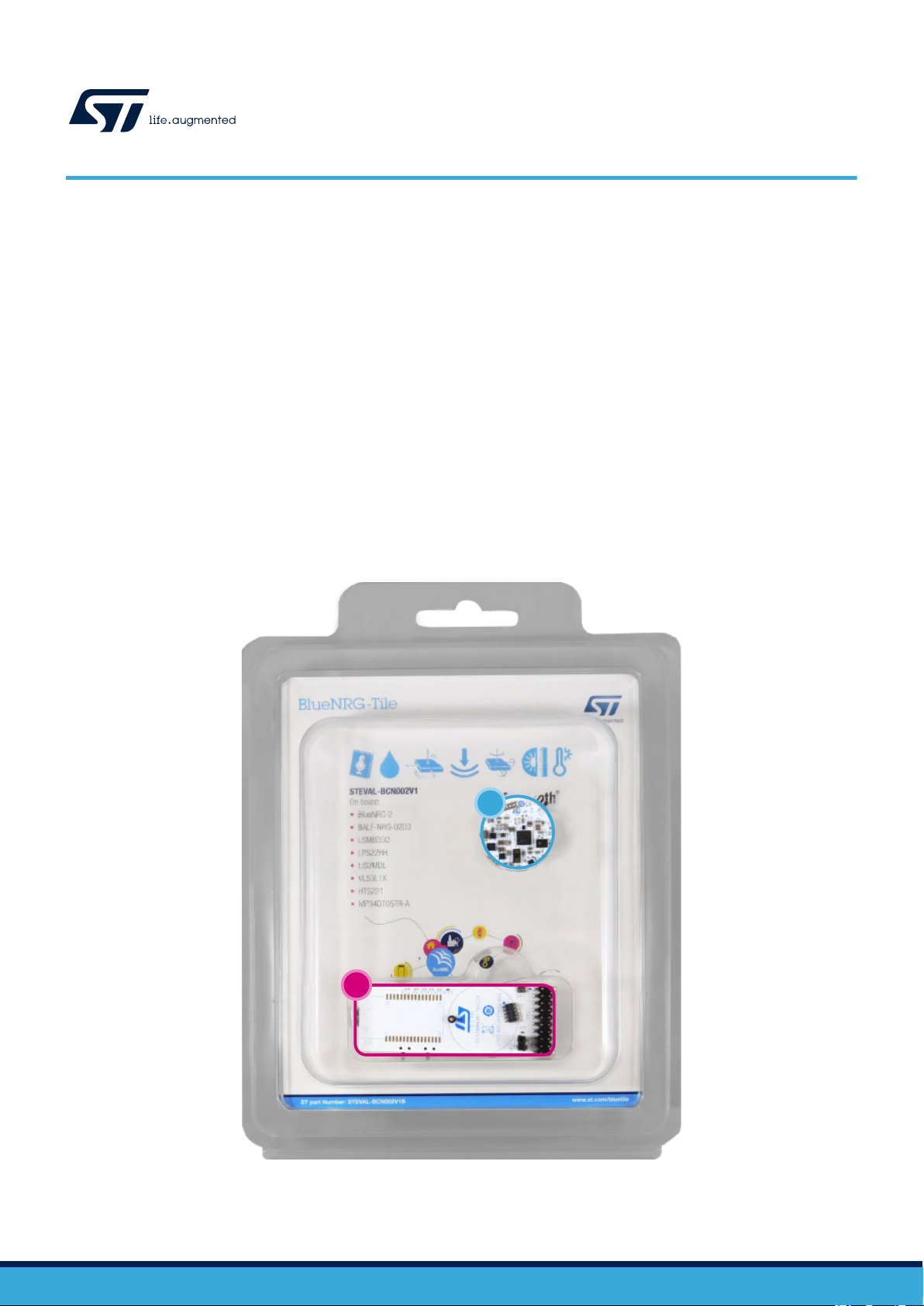
The STEV
board based on BlueNRG-2 SoC Bluetooth Low Energy application processor. This sensor board has accelerometer,
gyroscope, magnetometer, pressure, humidity, Time-of-Flight and microphone sensors, and is powered by a common CR2032
coin battery.
The sensor board communicates with a Bluetooth LE enabled smartphone running the ST BLE Sensor app, available on Google
Play and iTunes stores.
The STEVAL-BCN002V1D adapter board is used to program and debug the sensor board. The adapter board is powered via
USB.
1. STEVAL-BCN002V1 “BlueTile” sensor node with inertial and environmental digital MEMS sensors, a digital MEMS microphone, a time-offlight proximity sensor and a Bluetooth 5.0 wireless system-on-chip with a Cortex-M0 core
2. STEVAL-BCN002V1D host board to Flash and debug the sensor node
AL-BCN002V1B Bluetooth LE enabled sensor node development kit features the STEVAL-BCN002V1 multi-sensor
Figure 1. STEVAL-BCN002V1B BlueTile kit
UM2501 - Rev 3 - June 2020
For further information contact your local STMicroelectronics sales of
fice.
www.st.com
Page 2

1 Safety Information
Any type of usage not specified by the manufacturer may compromise the protection mechanisms in the device.
1.1 Class 1 laser product
VL53L1X contains a laser emitter; the device is designed to limit the laser output within Class 1 laser safety limits
under all conditions including single faults, in compliance with IEC 60825-1:2014 (third edition).
Recommended settings and operating conditions specified in VL53L1X datasheet and user manual MUST be
respected.
The laser output MUST NOT be increased by any means and no optics should be to used focus the laser beam.
Use of controls or adjustments or performance of procedures other than those specified in VL53L1X datasheet
and user manual may result in hazardous radiation exposure.
UM2501
Safety Information
UM2501 - Rev 3
page 2/44
Page 3
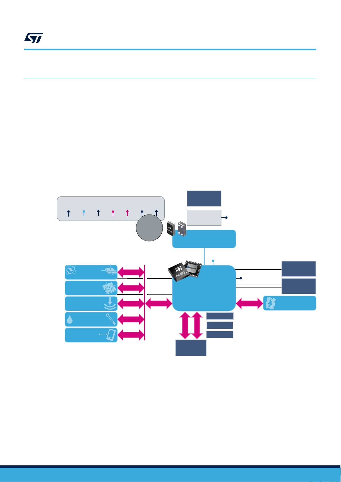
2 STEVAL-BCN002V1 BlueTile sensor node
I2C
LPS22HH
RGB LED
user button
UART
MP34DT05-A
LIS2MDL
32 MHz
I2C
I2C
VL53L1
400
kHz
1.6
I2C
Test points
TEST
VDDGND
MHz
RFTEST
PDM
inductor
10 pin
connector
32 KHz
Integrated
antenna
LSM6DSO
UART_RX line
I2C
BALF-NRG-02D3
HTS221
I2C
TEST ADC
ADC
RFTEST
SWD
SDASCL
IRQ
IRQ
I2C
3 VO LTS
+
BlueNRG-2
d
Pi-network
BlueTile is a small form-factor reference design ready for you to extend and customize, as well as a development
platform for BLE-enabled applications using the BlueNRG-2
and evaluate the performance of the sensors and the capabilities of the BLE.
Thanks to its small and thin design, BlueTile can be used in the field for data collection activities to test and
develop new algorithms.
Figure 2. STEVAL-BCN002V1 BlueTile block diagram
BlueNRG-2: Bluetooth 5.0 network and application processor
LSM6DSO: accelerometer and gyroscope
LIS2MDL: magnetometer
LPS22HH: barometer
HTS221: relative humidity and temperature sensor
VL53L1X: time-of-flight proximity sensor
MP34DT05-A: microphone
BALF-NRG-02D3: integrated balun
SDK. It is also an evaluation tool to help you assess
UM2501
STEVAL-BCN002V1 BlueTile sensor node
UM2501 - Rev 3
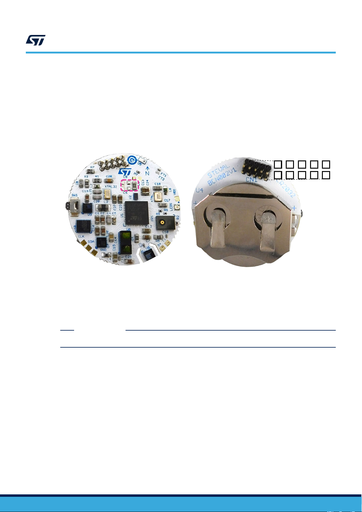
• The integrated SMD antenna needs clearance area and passives for proper tuning (FT1, FT2 and MT).
•
The Pi-network is only intended for flexibility and for testing. It is not populated as the integrated balun
provides the necessary matching.
• The 32kHz crystal allows lower power consumption BLE Sleep Mode.
• The inductor allows lower power consumption in BLE Active Mode.
• The STEVAL-BCN002V1 BlueTile sensor node is supplied with the default firmware (BLE_SensorDemo,
available in the SDK) already loaded. The firmware enables the streaming of sensor data to the reference
smartphone app (ST BlueMS, available on Android™ and iOS™ stores).
page 3/44
Page 4
1a
2a
4a
5a
6a
2b
2c
2d
2e
2f
3b
4b
4c
4d
4e
4f
4g
4h
1b
5b
6b
7a
7b
8
RESETN
UART RX
UART TX
SWD CLK
SWD IO
IO IO IO IO
GND
BOOT
GND GND VDD
1
2
10
UM2501
System architecture
Figure 3. STEV
1a. BlueNRG-2 Bluetooth 5.0 network and application processor 1b. BALF-NRG-02D3 integrated balun and matching network
2a. LPS22HH ambient pressure sensor 2b. LSM6DSO smart accelerometer and gyroscope 2c. LIS2MDL magnetometer 2d.
VL53L1X proximity by time-of-flight 2e. HTS221 relative humidity and temperature 2f. MP34DT05-A top-port digital microphone
3a. User button 3b. RGB LED
4a. I2C SCL 4b. I2C SDA 4c. GND 4d. ADC 4e. TEST 4f. VDD 4g. GND 4h. RFTEST
5a. II-network (not mounted) 5b. SMD antenna
6a. Inductor to enable lowest power BLE active mode 6b. 32kHz crystal to enable lowest power BLE sleep mode
7a. Battery holder 7b. CR2032 battery (not included)
8. 10-pin connector
FCC ID: S9NSTEBCN2V1 IC ID: 8976C-STEBCN2V1
AL-BCN002V1 sensor node front and rear components
The BlueTile sensor node is supplied with the firmware already loaded. The default firmware includes two
libraries:
1.
MotionFX fusion library for orientation estimation (visualized with a rotating cube).
2. BlueVoice library to stream the voice captured by the MEMS microphone over the BLE connection
(reproduced by the smartphone speaker, if not in vibration mode).
The STBLESensor app can be used to plot and log sensor data in real time on your smartphone.
RELATED LINKS
STBLE sensor documentation
2.1 System architecture
The BlueTile is powered by a coin-cell battery (CR2032). The voltage is not regulated because the sensors and
the BlueNRG-2
embedded linear power regulator and switching mode power converter (DC-DC).
2.1.1 Power section for BlueNRG-2
The BlueNRG-2 in active mode can use the embedded linear voltage regulator (LDO) or the embedded DC-DC
converter (DC-DC).
•
LDO regulator [Active mode, CPU Flash and RAM on]:
– RX 14.5 mA at 3 V, TX 17.2 mA when output power is +2 dBm
– range is 12-28.8 mA when output is -14 to +8 dBm
• DC-DC converter [Active mode, CPU Flash and RAM on]:
– RX 7.7 mA at 3 V, TX 9 mA at 3 V when output power is +2 dBm
– range is 6.6-15.1 mA when output is -14 to +8 dBm
UM2501 - Rev 3
can all operate at the voltage range of the battery. In any case, the BlueNRG-2 has its own
page 4/44
Page 5

System architecture
Note: The BlueTile sensor node includes the inductor needed by the DC-DC converter to allow lower power
consumption in active mode.
In Sleep Mode, the BlueNRG-2 device can use its internal 32 kHz ring oscillator (RO) or the external 32 kHz
crystal oscillator (XO) available on the BlueT
mode:
• Sleep Mode [32 kHz ring oscillator, 24 kB RAM retention]: 2.1 µA at 3 V
• Sleep Mode [32 kHz crystal oscillator, 24 kB RAM retention]: 0.9 µA at 3 V
ile sensor node, which offers lower power consumption in sleep
2.1.2 Radio frequency section
The radio frequency section of the BlueTile includes the following elements:
1.
A BALF-NRG-02D3 ultra-miniature balun which integrates matching network and harmonics filter.
2. A Pi-network which allows additional filtering and provides access points for testing.
Note: This network is not populated, as the integrated balun provides the necessary matching.
3. An SMD 2.4 GHz antenna, which requires a certain clearance area on the PCB and specific passives for
precise tuning (FT1, FT2 and MT).
2.1.3 MEMS sensor section
The MEMS sensor section of the BlueTile sensor node includes inertial and environmental MEMS sensors
connected with the BlueNRG-2 via an I2C bus operating at 400 kHz.
The MEMS microphone is connected with BlueNRG-2 through a dedicated line to transfer the PDM (Pulse
Density Modulated) stream at 1.6 MHz, which is converted to PCM (Pulse Coded Modulation) by the integrated
digital filter in the ADC block on the BlueNRG-2.
All sensors can generate interrupts, but only the interrupts from the LIS2MDL magnetometer and the LSM6DSO
accelerometer and gyroscope are connected with the BlueNRG-2 through dedicated and independent lines.
•
The LIS2MDL magnetometer interrupt line is push-pull only and must have its own independent line. The
interrupt pin of this sensor is connected with BlueNRG-2 to enable applications such as “reed-switch”, which
is activated by an external magnet.
• The LSM6DSO smart accelerometer and gyroscope interrupt pin is an input at boot. It has an internal pulldown. If the pin is low at boot, the I2C interface is selected, otherwise the I3C interface is selected. The pin
can be reconfigured as open-drain, but the external pull-up would cause additional power consumption. The
interrupt pin of this sensor is connected to BlueNRG-2 to exploit the smart embedded processing
functionality (single/double tap recognition, free-fall, wakeup, portrait/landscape, 6D/4D orientation detection;
activity/inactivity, stationary/motion detection; pedometer, step detector and step counter; up to 16 finite state
machines to process).
• The LPS22HH barometer interrupt pin exhibits the same behavior as the LSM6DSO interrupt pin: it is an
input pin at boot and must be low to activate the I2C interface. It can be configured as push-pull or opendrain after boot. The interrupt pin of this sensor is not connected to BlueNRG-2.
• The HTS221 relative humidity and temperature interrupt pin is push-pull at boot and can be reconfigured as
open-drain after boot. The interrupt pin of this sensor is not connected to BlueNRG-2.
• The VL53L1X time-of-flight proximity interrupt line is open-drain only and would require an external pull-up.
The interrupt pin of this sensor is not connected to BlueNRG-2.
The dynamics of the environmental parameters are relatively slow, so interrupts are not necessary. The
application only needs to wake up every few seconds and perform one-shot measurements with the LPS22HH
barometer or HTS221 relative humidity and temperature sensor, and trigger an action if specific conditions are
met.
It is also not convenient to keep the VL53L1X proximity time-of-flight sensor active, the power consumption or the
latency would be too high. The power consumption of VL53L1X ranges from 0.5 mA for 1 Hz measurements, up
to 7 mA for 10 Hz measurements.
UM2501
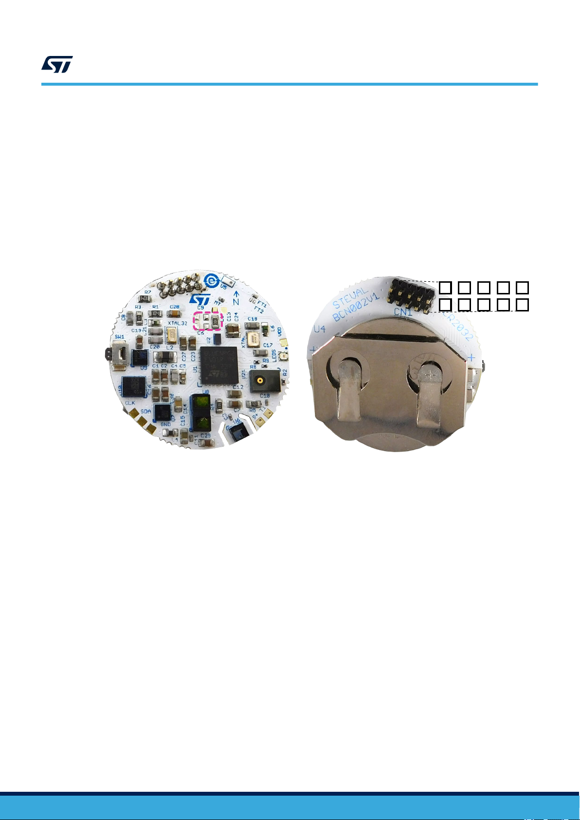
2.1.4 Pinout descriptions
In the following figure, you can see 6 pads along the edge of the board:
•
RFTEST (4h) and GND (4g) connected to the RF section for test purposes.
• TEST (4e) connected to the analog TEST output of BlueNRG-2 for test purposes.
• VDD (4f) and GND (4c), for test purposes or to power additional external components.
• ADC (4d) to accept analog input signals from additional external components.
UM2501 - Rev 3
page 5/44
Page 6
1a
2a
4a
5a
6a
2b
2c
2d
2e
2f
3b
4b
4c
4d
4e
4f
4g
4h
1b
5b
6b
7a
7b
8
RESETN
UART RX
UART TX
SWD CLK
SWD IO
IO IO IO IO
GND
BOOT
GND GND VDD
1
2
10
Features of the BlueNRG-2 device
• I2C SCL (4a) and I2C SDA (4b) to connect additional external components via I2C.
UM2501
Figure 4. STEV
1a. BlueNRG-2 Bluetooth 5.0 network and application processor 1b. BALF-NRG-02D3 integrated balun and matching network
2a. LPS22HH ambient pressure sensor 2b. LSM6DSO smart accelerometer and gyroscope 2c. LIS2MDL magnetometer 2d.
VL53L1X proximity by time-of-flight 2e. HTS221 relative humidity and temperature 2f. MP34DT05-A top-port digital microphone
3a. User button 3b. RGB LED
4a. I2C SCL 4b. I2C SDA 4c. GND 4d. ADC 4e. TEST 4f. VDD 4g. GND 4h. RFTEST
5a. II-network (not mounted) 5b. SMD antenna
6a. Inductor to enable lowest power BLE active mode 6b. 32kHz crystal to enable lowest power BLE sleep mode
7a. Battery holder 7b. CR2032 battery (not included)
8. 10-pin connector
FCC ID: S9NSTEBCN2V1 IC ID: 8976C-STEBCN2V1
AL-BCN002V1 sensor node front and rear components
On the debug connector on the rear of the board, there are 10 pins:
VDD (pin 2) and GND (pin 4, 6, 10) to accept power from the host motherboard.
•
• SWD IO (pin 1) and SWD CLK (pin 3) to Flash and debug through the host motherboard.
– SWD pins can be used as digital GPIOs when the BlueTile is not connected to its host board.
• UART TX (pin 5) and UART RX (pin 7).
– UART pins can be used as digital GPIOs when the BlueTile is not connected to its host board.
• BOOT (pin 8) and RESETN (pin 9) to control the boot and keep BlueNRG-2 under reset.
– The boot pin can also be used as a digital GPIO when the BlueTile is not connected to its host board,
but it needs to be pull-down at start-up.
2.2 Features of the BlueNRG-2 device
BlueNRG-2 integrates a Bluetooth Low Energy radio (BLE), an ARM® Cortex®-M0 core, 12+12 kB of RAM,
UM2501 - Rev 3
256 kB of Flash memory
fast 400 kHz), UART interfaces; two multi-function timers (MFT), a DMA controller, RTC and watchdog, and an
ADC with PDM stream processor.
The public key cryptography (PKA) and random number generator (RNG) are reserved for the BLE protocol stack,
but the user application can also read the RNG.
The ADC is 10-bit and features single or continuous acquisition at max. 1 MHz sampling frequency, two single
ended or one differential signal (ADC1 and ADC2 pins), embedded channels for temperature and battery voltage
sensing, embedded digital filter with down sampling. The embedded digital filter can be used to process the PDM
stream from a digital MEMS microphone (1.6 MHz or 0.8 MHz) and convert it to audio PCM (8 kHz to 50 kHz
when 1.6 MHz clock is used for the microphone).
BlueNRG-2 uses the embedded digital filter of the ADC peripheral for PDM to PCM conversion when reading the
PDM output of the MEMS microphone MP34DT05-A.
, SPI (max 1 MHz in slave mode, 8 MHz in master mode), two I2Cs (standard 100 kHz or
page 6/44
Page 7

The low-speed clock is used in low-power mode and can be supplied by the internal RC oscillator or by an
external crystal (32 kHz ±50 ppm). The high-speed clock is supplied by a fast-starting internal RC oscillator
(16 MHz) while the external crystal is starting up. The high-speed external crystal (16 or 32 MHz) is required to
enable the BLE radio.
Only the 32 MHz XO can support the highest computational loads, allowing the Cortex-M0, the DMA and the APB
tree to run at 32 MHz, while the rest of the clock tree runs at 16 MHz. When a 16 MHz XO is used, the Cortex-M0
and all the clock tree runs at 16 MHz.
2.2.1 BlueNRG-2 states
• Preactive:
–
After power-on-reset, all digital power supplies are stable.
– Internal 16 MHz and 32 kHz RC oscillators are used.
– Reachable from Reset, Standby and Sleep states.
– Goes to Active state.
• Active:
– The external high-frequency crystal is used (16 MHz ±50ppm or 32 MHz) to enable BLE
communication.
– Internal 16MHz RC oscillator is switched off
– BlueNRG-2 uses a 32 MHz ±10ppm crystal (higher crystal accuracy = lower power consumption).
– The radio can be activated for transmission (TX) or reception (RX). This is the state used by
BlueNRG-2 when the user application is running or there is a BLE event to serve.
– The programmed GPIO configuration is restored.
– reachable only from Preactive only.
• Standby:
– RAM retention is used (12 or 24 kB).
– 5 different GPIOs can be used to wake-up: IO9, IO10, IO11 with an internal pull-up; IO12, IO13 which
require an external drive).
– BlueNRG-2 IO11 is connected to the user button, IO12 connected to the interrupt pin of LIS2MDL
magnetometer, and IO13 connected to the interrupt pin of the LSM6DSO accelerometer and
gyroscope.
– Wake-up time is typically 200µs.
– reachable from Active.
– can go to Preactive.
• Sleep:
– RAM retention is used (12 or 24 kB).
– The low-frequency oscillator is switched on to serve periodic BLE connection events.
– 5 different GPIOs can also be used to wake-up, as in Standby state.
– This is the state used by the BlueNRG-2 tile to save power when the user application is not running
and the device is waiting for a BLE event to serve.
– The programmed GPIO configuration is not maintained (this may affect connected sensors; for
example, see pin IO7 of BlueNRG-2 connected to XSHUT pin of VL53L1X).
– Reachable from Active.
– Can go to Preactive.
UM2501
Features of the BlueNRG-2 device
2.2.2 BLE firmware stack and memory map
Program memory, data memory, registers and I/O ports are organized in a linear 32-bit address space.
•
The SRAM is divided in two banks:
– 12 KB from 0x2000_0000 to 0x2000_2FFF (retention always-on).
– 12 KB from 0x2000_3000 to 0x2000_5FFF (retention optional).
– The FULL BLE stack needs 9.6 KB of SRAM.
– The BASIC BLE stack needs 8.0 KB of SRAM.
UM2501 - Rev 3
page 7/44
Page 8

UM2501
Inertial MEMS sensors
• The Flash is 256 KB from 0x1004_0000 to 0x1007_FFFF
–
The FULL BLE stack needs 77 KB, leaving 179 KB for the user application. The FULL BLE stack
supports concurrent peripheral and central roles (N=0,1,2 connections to other centrals and 8-N
connections to other peripherals), LE secure connections, controller privacy, and extended data length.
– The BASIC BLE stack needs 58 KB, leaving 198 KB for the user application. The BASIC BLE supports
the peripheral role only (1 connection to a central), legacy security only, no controller privacy and no
extended data length.
– The OTA manager for over-the-air firmware updates adds 10 KB to the size of the BLE stack.
The OTA manager may be independent of the user application, or embedded in the user application:
• When the OTA manager is independent of the user application, the Flash is divided in two sections:
1. A relatively small section for the OTA application; the size is the sum of the BLE stack size and the
OTA manager size.
2. A larger section for the user application.
• When the OTA manager is embedded in the user application, the Flash is divided in three sections:
1. A section that holds the current application; the size is the sum of BLE stack size, OTA manager size
and user application size.
2. A section for the new updated application; the size is the same as the first section.
3. A very small section for the reset application that decides decides which application to run after boot,
depending on what is available and valid in the first two sections.
An independent OTA manager leaves more room for the user application, but there is no application to run if the
update does not finish successfully.
An embedded OTA manager can still use the previous application if the update does terminate successfully, but
the space available for the user application is less than half the size of the Flash.
Note: After a successful update, the new application can be copied over the old application, or the role of the first two
sections can be exchanged.
2.3 Inertial MEMS sensors
Each sensor is made of a Micro Electro Mechanical system (MEMS) with a sensing element and a dedicated
ASIC with analog acquisition chain, analog-to-digital converter (ADC), and digital signal processing (DSP) and
control logic.
2.3.1 LSM6DSO 3D accelerometer and 3D gyroscope
2.3.1.1 LSM6DSO interrupts
The LSM6DSO delivers best-in-class motion sensing able to support more sophisticated functionality than simply
orienting devices to portrait and landscape mode.
The following event-detection interrupts are supported:
•
Free-fall event:
– detected when acceleration data from all enabled axes are below threshold settings for a certain
duration
• Wake-up event:
– detected when the filtered data from any of the enabled axes are above threshold settings for a certain
duration
– choose between high-pass filtered data, slope detection filter (difference between consecutive
samples, divided by two), low-pass filtered data plus an offset for each axis, or unfiltered data plus an
offset.
• 6D/4D orientation event:
– detected when an axis (positive or negative) is above the threshold setting, while the other two are
below the threshold for a certain duration
– 4D is a subset of 6D; the Z axis is not used.
– choose between unfiltered data or low-pass filtered data
UM2501 - Rev 3
page 8/44
Page 9

UM2501
Inertial MEMS sensors
• Single/double tap event:
–
detected when the output of the slope detection filter exceeds the threshold setting and then returns
below the same setting within a “shock” time interval
– double tap event is detected when a first tap is detected and a second tap is detected after a “quiet”
time interval, but before a maximum “duration” interval
– for reliable detection, configure the device to use a high sampling rate, like 400 Hz.
– if two or more enabled axes are over their respective thresholds, the axis with the highest priority
setting is used
– can be used to enable user interaction in addition to the button present on the BlueTile
• Activity/inactivity event:
– uses the same data as the wake-up event
– if inactivity is detected (data below the threshold setting for a certain time interval), the device
automatically goes to Low-power Mode and reduces the accelerometer sampling rate down to 12.5 Hz
to minimize power consumption
– if a wake-up event is detected, the device automatically returns to the programmed accelerometer
operating mode and sampling rate
– can be configured to put the gyroscope in power-down or sleep mode when the accelerometer is in
low-power mode
• Stationary/motion event
• a special activity/inactivity event in which event detection is the same, but the device does not change power
mode or sampling rate
2.3.1.2 LSM6DSO advanced functionality
Certain digital processing blocks allow advanced functions and algorithms when the output data rate is 26 Hz or
higher
.
• Pedometer functions: step detector and step counter.
– when a step is detected, an interrupt is generated and a corresponding counter is incremented by 1
(max value is 65535)
– can also set the interrupt to only be triggered when at least one step is detected in a configurable time
interval
– de-bounce functionality to avoid false detections, where N consecutive steps are detected before the
first interrupt is generated (default is N=10)
– two additional blocks can facilitate the identification of false-positives:
only trigger when statistical data matches the walking pattern
adapt the embedded algorithm to slow pace walking patterns
• Significant motion detection: to signal a possible change in user location
– based on the pedometer function, which is automatically enabled
– interrupt is generated when the difference between the number of steps after initialization or reset is
higher than the de-bounce threshold (default is 10).
– function is reset after each interrupt
• Relative tilt detection
– generates an interrupt when there a change in the tilt of the device exceeds 35 degrees
– reference position is set when the detection logic is enabled and reset when the interrupt is generated
– detection logic requires a 2-second settling time after it is enabled or re-initialized
2.3.1.3 LSM6DSO finite state machines
The LSM6DSO can run up to 16 simultaneous finite state machines (FSMs) that consist of a sequence of
instructions or actions (parameter setting, interrupt generation, etc.), or a RESET
• if the RESET condition is satisfied, the FSM returns to the reset point
• if the NEXT condition is satisfied, the FSM moves to the next instruction
• otherwise, the RESET-NEXT conditions are re-tested.
FSM data may be accelerometer, gyroscope, integrated gyroscope or external sensor data, and can be
decimated. A data vector consists of X, Y, Z values and a vector norm V (square root of sum of squares).
UM2501 - Rev 3
-NEXT condition:
page 9/44
Page 10

Each FSM has the following features:
•
3 different 8-bit masks to allow tests on positive and negative values of X, Y, Z and V.
• 3 different thresholds and 1 programmable hysteresis value that is automatically added to or subtracted from
the selected threshold based on the test condition.
• 4 different counters/timers to manage event durations.
2.3.1.4 LSM6DSO smart FIFO buffer
The LSM6DSO accelerometer has a first-in first-out (FIFO) data buf
words of 7 bytes each (1 tag byte plus 6 data bytes). The tag drives the decoding and includes a parity bit for
validation, while the data can derive from any combination of accelerometer, gyroscope, up to 4 external sensors,
embedded temperature sensor, timestamp counter and pedometer step counter. The data rates can be set
independently for each source.
For the accelerometer, you can choose to store high-pass filtered data, slope detection filter data, low-pass
filtered data or unfiltered data plus an optional offset (independent for each axis). The low and high-pass filters
are configurable.
For the gyroscope, you can enable a first optional high-pass filter, and a second optional and programmable lowpass filter.
To maximize the amount of data stored in the FIFO, you can enable an adaptive lossless delta pulse-codedmodulation (DPCM) compression algorithm for the accelerometer and the gyroscope data. When the difference
between consecutive data words is small, instead of sending a new data word (16 bits/axis), only the difference
with respect to the previous is sent (8 bits = 2:1 compression or 5 bits/axis = 3:1 compression).
When DPCM compression is enabled, it is also possible to select when DPCM is reset by storing uncompressed
data in the FIFO: never, every 8, 16 or 32 words. This is useful when the FIFO is used as a circular buffer
(Continuous mode) and words may be overwritten, as the decoder can only work if previous data words can be
traced back to an uncompressed data word for reference.
DPCM compression works on 3 data words (sampled at time t, t-1 and t-2) and introduces a latency of 2 data
words. The compression factor depends on the difference between a data word and the previous data word.
• When DPCM is disabled, the compression buffer is flushed and the output is the non-compressed data word
at time t-2, then data word at time t-1 and data words at current time t thereafter (tag “NC_T_2”, “NC_T_1”,
and “NC”).
• When DPCM is enabled, the first output is the non-compressed data word at time t-2 (tag “NC_T_2”), used
as the reference to start decoding. Subsequent outputs depend on D2 (difference between data word at t-2
and previous decoded word), D1 (difference between data word at t-1 and t-2), and D0 (difference between
data word at t and t-1):
– If any difference in D2 exceeds 128 LSB on any axis:
◦ the uncompressed data word at time t-2 is written to the FIFO by storing the 16-bit signed value of
each axis (low and high bytes for X, Y and Z: XL XH YL YH ZL ZH, for a total of 6 bytes)
◦ tag NC_T_2
– If any difference in D2 and D1 exceeds 16 LSB, but is within 128 LSB for all axes:
◦ a 2:1 compression ratio is applied by storing the 8-bit signed difference to reconstruct 2 data
values for each axis at time t-1 and t-2 (D1x D1y D1z, then D2x D2y D2z, for a total of 6 bytes)
◦ tag 2xC
◦ the data at time t-2 is derived by summing D2 to the previously decoded data word
◦ the data at time t-1 is derived by summing D1 to the data at time t-2 just derived
– If all differences in D2, D1 and D0 are within 16LSB for all axis:
◦ a 3:1 compression ratio is applied by storing the 5-bit signed difference to derive 3 data values for
each axis at time t, t-1 and t-2 (D0x D0y D0z and a dummy bit to make 16 bits, then D1x D1y D1z
and a dummy bit, then D2x D2y D2z and a dummy bit, for a total of 6 bytes)
◦ tag 3xC
◦ the data at time t-2 is derived by summing D2 to the previous decoded data word
◦ the data at time t-1 is derived by summing D1 to the data at time t-2 just derived
◦ the data at time t is derived by summing D0 to the data at time t-1 just derived
Interrupts can be generated when the FIFO buffer stores a given number of samples (FIFO threshold level), or
when it is full, or when it overflows (overrun). The FIFO can work in the following modes:
UM2501
Inertial MEMS sensors
fer that can store up to 3 KB of data, or 512
UM2501 - Rev 3
page 10/44
Page 11

Inertial MEMS sensors
• Bypass Mode:
–
the FIFO buffer is disabled and cleared
• FIFO Mode:
– the FIFO buffer collects data until it is full, then stops
• Continuous Mode:
– the FIFO buffer collects data continuously
– when it is full, the oldest samples are overwritten as in a circular buffer
– FIFO full and FIFO threshold level interrupts allow the host microcontroller to read the data before it is
overwritten
• Continuous-to-FIFO Mode:
– the FIFO buffer collects data continuously but switches to FIFO Mode as soon as the selected interrupt
occurs
– this mode is especially useful to capture data before and after a specific event
• Bypass-to-Continuous Mode:
– the FIFO buffer is disabled, but switches to Continuous Mode as soon as the selected interrupt occurs
– this mode is useful to capture data after an event has occurred
• Bypass-to-FIFO Mode:
– the FIFO buffer is disabled, but switches to FIFO mode as soon as the selected interrupt occurs
– this mode is useful to capture data after an event has occurred
– data collection stops once the FIFO is filled
UM2501
UM2501 - Rev 3
page 11/44
Page 12

2.3.2 LIS2MDL 3-axis magnetometer
2.3.2.1 LIS2MDL dynamic range, resolution and accuracy
The LIS2MDL
Gauss if the magnetic field is not aligned with one of the axes), which is well above Earth’s magnetic field (which
is typically in the range of 0.25 to 0.65 Gauss).
The output is 16 bits (1.5 mGauss/LSB ±7%), and the RMS noise level in High-performance Mode is 3 mGauss
(2 LSB). The high resolution and accuracy allows e-compass orientation estimation and distance measurements
from a reference magnet (in its simplest form, the magnetometer can emulate a magnetically activated Reedswitch).
The LIS2MDL magnetometer can perform a single-shot measurement and then return to Power-down Mode, or
operate in Continuous Mode with a programmable sampling rate (10, 20, 50 or 100 Hz).
Single-shot measurements can be performed at max. 100 Hz in high-performance mode, or max. 150 Hz in lowpower mode. In low-power mode, the power consumption is reduced to 25%, while in high-performance mode the
RMS noise is halved. An optional low-pass filter can be activated to further reduce RMS noise, without increasing
the power consumption, the bandwidth in this case is reduced from output data rate ODR/2 down to ODR/4.
2.3.2.2 LIS2MDL intrinsic offset automatic cancellation
The LIS2MDL
an initial operating condition; a reset pulse may be used to enable the compensation of the intrinsic magnetic
offset.
• If intrinsic offset compensation is disabled, there is no reset pulse. The set pulse can be generated at poweron only (Set_FREQ=1), or every 64 measurements (Set_FREQ=0).
• If intrinsic offset compensation is enabled, set and reset pulses are generated alternately on consecutive
samples. After the set pulse, the measured output is the magnetic field H plus offset; after the reset pulse,
the measured output is H minus offset.
– In Continuous Mode, the device averages consecutive measurements to compensate for the offset, the
– output =
– In Single-shot Mode, the host microcontroller averages two consecutive measurements. The averaged
When intrinsic offset compensation is performed, the residual offset is in the range of ±60 mgauss, and the
dependency on temperature is ±0.3 mgauss/°C.
is a 3D digital magnetometer with a ±50 Gauss dynamic magnetic field range (reduced to ±25
is based on anisotropic magneto-resistive (AMR) technology, in which a set pulse is required to set
output will be equal to the magnetic field H.
ffset
H + o
+ H − offset
2
= H
measurements must occur within a short time of each other for the compensation to be ef
UM2501
Inertial MEMS sensors
fective.
2.3.2.3 LIS2MDL extrinsic offset (hard iron) compensation
Hard-iron compensation is a constant offset added to magnetic field measurements to compensate distortion
caused by ferromagnetic materials or high currents. This of
analysing the output of the magnetometer.
When it is available, this offset can be programmed in specific registers (OFFSET_X_REG_H/L,
OFFSET_Y_REG_H/L, OFFSET_Z_REG_H/L) so that it is automatically subtracted by the LIS2MDL device.
RELATED LINKS
DT0059: Ellipsoid or sphere fitting for sensor calibration
MotionMC software library in the X-CUBE-MEMS1 Sensor and motion algorithm software expansion for STM32Cube
2.3.2.4 LIS2MDL interrupt generation
The LIS2MDL
the subtraction of hard-iron offset) exceeds a programmed threshold (INT_THS_H/L_REG) in the positive or
negative direction.
Comparisons can be enabled independently for each axis (XIEN, YIEN, ZIEN flags):
• when the output data is above the positive threshold, the corresponding flag is set (P_TH_S_X/Y/Z)
• when the output data is below the negative threshold, the corresponding flag is set (N_TH_S_X/Y/Z).
A specific interrupt can be generated if there is a measurement range overflow at the internal ADC.
magnetometer sensor can be configured to generate an interrupt when output data (before or after
fset can be computed by the host microcontroller by
UM2501 - Rev 3
page 12/44
Page 13

2.4 Environmental MEMS sensors
2.4.1 LPS22HH barometer
2.4.1.1 LPS22HH acquisition chain
The LPS22HH pressure sensor can perform a one-shot measurement and then return to Power-down Mode, or it
can operate in Continuous Mode with a programmable sampling rate (1, 10, 25, 50, 75, 100 or 200 Hz).
Measurements can be taken in normal Low-noise Mode, or in Low-power Mode to minimize current consumption.
When continuous mode is selected, Low-noise Mode is not available at 100 and 200 Hz. In all cases, an optional
low-pass filter can be enabled with a programmable cutoff frequency to reduce the noise level (the bandwidth is
reduced from output data rate ODR/2 down to ODR/9 or ODR/20).
The low-pass filter is reset when it is enabled. After reset, a specific settling time is required before the first
accurate sample on the output is available (9 or 20 samples must be discarded, respectively).
Two programmable offsets can be subtracted from measured data:
• First, offset compensation (always): the offset measured with one-point calibration (OPC) can be stored in
specific registers (RPDS) and then subtracted from subsequent measurements (OPC-compensated data =
data – RPDS*256). The low-pass filter, if enabled, will filter OPC-compensated data. Filtered and unfiltered
OPC-compensated data is stored in the FIFO.
• Second, auto-zero mode (optional): the offset-compensated (and possibly filtered) pressure measurements
are stored in specific registers (REF_P) when auto-zero is enabled (AUTOZERO or AUTOREFP set to 1)
and then subtracted from subsequent measurements (AZ-compensated data = data – REF_P). Filtered and
unfiltered OPC-compensated data or AZ-compensated data is stored in output registers.
UM2501
Environmental MEMS sensors
2.4.1.2 LPS22HH interrupt generation and FIFO buffer
The LPS22HH pressure sensor can be configured to generate interrupt events related to pressure acquisitions
and FIFO status (watermark reached, full, overrun, etc.).
The interrupt can be generated when a new pressure or temperature sample is available, or when the AZcompensated data exceeds a programmed threshold (THS_P) in the positive (PHE flag enables the comparison
with +THS_P) or negative (PLE flag enables the comparison with –THS_P) direction. The following configurations
are available:
1.
AUTOZERO=0 and AUTOREFP=0: interrupt logic is disabled; filtered and unfiltered OPC-compensated data
goes to FIFO and output registers.
2. AUTOZERO=1: interrupt logic is enabled; REF_P is set when interrupt is enabled; AZ-compensated data
goes to the interrupt logic and to the output registers, while filtered and unfiltered OPC-compensated data
goes to FIFO.
3. AUTOREFP=1: interrupt logic is enabled; REF_P is set when interrupt is enabled; AZ-compensated data
goes to interrupt logic, while filtered and unfiltered OPC-compensated data goes to FIFO and output
registers.
The FIFO buffer can store up to 128 pressure samples (24 bits each) and 128 temperature samples (16 bits
each). FIFO depth can be limited by stopping at the programmable watermark level. The FIFO can work in the
following modes:
• Bypass Mode:
– the FIFO buffer is disabled and cleared
• FIFO Mode:
– the FIFO buffer collects data until it is full or the watermark setting is reached, then stops
• Continuous (or Dynamic Stream) Mode:
– the FIFO buffer collects data continuously
– when it is full or the watermark setting is reached, the oldest samples are overwritten as in a circular
buffer
– FIFO full and FIFO threshold level interrupts allow the host microcontroller to read the data before it is
overwritten
UM2501 - Rev 3
page 13/44
Page 14

Environmental MEMS sensors
• Continuous (Dynamic Stream)-to-FIFO Mode:
–
the FIFO buffer collects data continuously but switches to FIFO Mode as soon as the selected interrupt
occurs
– this mode is especially useful to capture data before and after a specific event
• Bypass-to-Continuous (Dynamic Stream) Mode:
– the FIFO buffer is disabled, but switches to Stream Mode as soon as the selected interrupt occurs
– this mode is useful to capture data after an event has occurred
• Bypass-to-FIFO Mode:
– the FIFO buffer is disabled, but switches to FIFO mode as soon as the selected interrupt occurs
– this mode is useful to capture data after an event has occurred
UM2501
UM2501 - Rev 3
page 14/44
Page 15

2.4.2 HTS221 temperature sensor
2.4.2.1 LPS22HH vs HTS221 ambient temperature measurement
The temperature sensor in the LPS22HH device is designed to compensate for temperature ef
pressure measurements, while the temperature sensor in the HTS221 device is designed and characterized for
ambient temperature measurements.
The BlueTile takes ambient temperature data from the HTS221 because it is more accurate over a larger range
than the LPS22HH. However, applications requiring a high data rate (above 12.5 Hz) can take data from the
LPS22HH temperature sensor.
Table 1. Comparison of HTS221 and LPS22HH temperature sensor characteristics
UM2501
Environmental MEMS sensors
fects in ambient
Device
HTS221 -40 to +120 °C 64 LSB/°C
LPS22HH -40 to +85 °C 100 LSB/°C ±1.5 °C (0 to 80 °C)
Temperature sensor
operating range
2.4.2.2 HTS221 acquisition chain
While all the board components have an embedded temperature sensor to monitor the temperature of the silicon,
the embedded HTS221
has the physical properties and accuracy necessary for the measurement of ambient
temperature.
The raw output of the humidity acquisition chain is stored in two 8-bit registers (HUMIDITY_OUT_H and
HUMIDITY_OUT _L), which are concatenated into a 16-bit two’s complement value (H_OUT). The raw output is
already temperature compensated and calibration coefficients to derive Relative Humidity (RH) from raw humidity
data are stored in the device. Factory calibration is performed at two different humidity levels and one
temperature.
The following sequence is used to calculate RH:
1. First true RH during calibration: H0
2. Second true RH during calibration: H1
3. First raw H output during calibration: H0
4. Second raw H output during calib.: H1
5. Current raw H output: H_O
6. Current RH% by linear interpolation: RH = R
The raw output of the temperature acquisition chain is stored in two 8-bit registers (TEMP_OUT_H and
TEMP_OUT _L) which are concatenated into a 16-bit two’
derive the Temperature in °C from raw temperature data are stored in the device. Factory calibration is performed
at two different temperatures.
Follow the sequence below to calculate the temperature in °C:
1. MSB of true temperatures during calibration: T1T0M
2. First true T in Celsius deg. (two’s comp): T0
3. Second true T in Celsius deg. (two’s comp): T1_°C_x8 setT1°C =
4. First raw T output during calibration: T0
5. Second raw T output during calibration: T1
6. Current raw T output during calibration: T_O
7. Current Temperature in °C: T = T0d
Sensitivity
UT
setH = H_O
Temperature absolute
accuracy
±1°C (0 to 60 °C)
±0.5 °C (15 to 40 °C);
_rH_x2
setRH0
_rH_x2
_T0_OUT
_T0_OUT
UT
H0 +
_°C_x8
_OUT
setT0
_OUT
UT
T1d
eg +
eg − T0deg
Long term
=
setRH1
setH0
setH1
RH1 −
1, 7, 12.5 Hz
1, 10, 25, 50, 75,
100, 200 Hz.
_rH_x2
H0
2
H0_rH_x2
=
2
= H0_T0_OUT
= H1_T0_OUT
H − H0
*
RH0
H1 −
Data rate Response time
15 s (time to
63%).
- -
H0
s complement value (T_OUT). Calibration coefficients to
SB
setT0
setMSB1
°C =
= T1T0MSB&0x03,MSB0 =
_°C_x8 + MSB0*256
T0
8
T1
_°C_x8 + MSB1*256
8
T1T0M
= T0_OUT
setT1
= T1_OUT
setT = T _ O
T1 −
UT
* T − T0
T0
drift
0.05 °C/
year
.
SB
4
UM2501 - Rev 3
page 15/44
Page 16

2.4.2.3 HTS221 system integration
To get reliable and consistent measurements, the system design should maximize sensor exposure to the
external environment while minimizing error sources.
•
Mechanical design:
– if there is one vent hole in the BlueTile housing, the hole diameter should be maximized and the dead
volume enclosed should be minimized
– two or multiple vent holes are preferable in order to create a laminar airflow and minimize the response
time
– avoid materials that absorb humidity
• Mechanical stress:
– Avoid flexing or bending the BlueTile board
• Heat:
– Heat convection or temperature gradients on the board may affect the sensor
– Metal lines and planes, such as the ground plane, should be kept far from the sensor
– Milled slits further increase decoupling
– Insulation may be required to isolate the BlueTile from convective and conducted heat
• Light exposure may induce a change in temperature and humidity.
To accelerate sensor recovery time in case of condensation, the firmware running on the host microcontroller can
be coded to switch the heating element on for a certain duration. Humidity and temperature data should not be
read during the heating cycle.
The BlueTile is designed for ultra-low power operation and a long battery life (1 month to 1 year on a typical
CR2032 coin battery, depending on the application). Power and heat generated on-board is therefore very limited.
Possible sources of conducted heat such as the BlueNRG-2 and the LED are placed as far as possible from
MEMS sensors to avoid any impact on measurements. Slits are also present to further isolate the HTS221
temperature sensor from neighboring components.
UM2501
Environmental MEMS sensors
RELATED LINKS
AN4722: HTS221 digital humidity sensor: hardware guidelines for system integration
UM2501 - Rev 3
page 16/44
Page 17

2.5 MP34DT05-A digital MEMS microphone
2.5.1 Features of the MEMS microphone
The MP34DT05-A omnidirectional top-port digital microphone has the following features:
122.5 dBSPL acoustic overload point (AOP), or 0 dBFS (100% of digital Full Scale(FS))
•
• -26dBFS ±3dB (5% of FS) sensitivity at 1 kHz and 94 dBSPL
• 64dB A-weighted SNR
• The equivalent input noise floor is 30 (94-64) dBSPL, or -90 (-26-64) dBFS (0.003% of FS).
• The total harmonic distortion plus noise THD+N:
– 0.2% at 94 dBSPL
– 0.7% at 110 dBSPL
– 6% at 120 dBSPL
• The frequency response is generally flat from 100 Hz to 5 kHz, up to +0.5 dB at 20 kHz.
Appropriate frequency response is important to maximize the performance of beamforming applications that can
determine the direction of incoming sounds and reject noise coming from certain directions
RELATED LINKS
AcousticBF software library in the X-CUBE-MEMSMIC1 Digital MEMS microphones acquisition and processing software
expansion for STM32Cube
UM2501
MP34DT05-A digital MEMS microphone
2.5.2 PDM to PCM conversion
The output of the digital MEMS microphone is a bit stream (1.6 MHz on the BlueTile), where frequency of ones is
proportional to the sound pressure level: this is known as pulse-density modulation (PDM). However
usually represented by words with at least 16 bits, at a rate equal or greater than twice the max. audio frequency,
typically 16, 24 or 48 kHz: this is known as pulse-coded modulation (PCM).
The PDM-to-PCM conversion can be performed with low-pass filtering. In its simplest form, it is equivalent to
averaging, or counting the number of ones over the sampling time of the PCM word.
In the BlueTile the conversion is performed by hardware in a dedicated block in the ADC peripheral in BlueNRG-2
device, but the conversion can also be performed by software.
RELATED LINKS
AN4957: How to synchronize the DFSDMs filters and how to program the pulse skipper on the STM32F413/423 line devices
AN3998: PDM audio software decoding on STM32 microcontrollers
PDM2PCM software library in the X-CUBE-MEMSMIC1 Digital MEMS microphones acquisition and processing software
expansion for STM32Cube
, audio is
UM2501 - Rev 3
page 17/44
Page 18

2.6 VL53L1X Time-of-Flight sensor
2.6.1 Features of the Time-of-Flight sensor
The VL53L1X is a state-of-the-art laser-ranging sensor in a miniaturized package, with a 940 nm Class 1 verticalcavity surface-emitting laser (VCSEL), a receiving 16x16 array of single-photon-avalanche-detectors (SP
physical infrared filters and optics to achieve the best ranging performance.
The VL53L1X measures the time it takes for photons emitted by the laser to be reflected back to the sensor.
The field-of-view (FoV) is programmable from 15 to 27 degrees, which sets the region of interest (ROI) in the
SPAD array from 4x4 to 16x16 detectors, respectively. The position of the ROI in the array can also be set, in
order to orient the FoV cone in a specific direction.
The sensor returns the following data:
• ranging distance in mm
• the return signal rate and the ambient signal rate (kilo-count-per-second (kcps) per SPAD)
• range status
2.6.2 Calibration for best performance
For best performance, run the calibration functions at least once after assembly is completed. Calibration data is
stored in the host microcontroller and loaded in the VL53L1X on each startup.
If you call one or more calibration functions, you must observe the sequence below:
•
RefSPAD calibration:
– Optimizes device dynamics and accuracy.
– Especially recommended if a protective glass cover is used on top of the device.
– SPAD cells are classified as non-attenuated, attenuated by 5 or attenuated by 10.
– SPAD are then selected to avoid internal signal saturation.
– This part-to-part value is computed during the final test at ST and stored in the non-volatile memory
(NVM); it is automatically loaded after boot.
• Offset calibration:
– Should always be performed after assembly.
– Compensates for part-to-part variations, reflow effects, and cover glass effects.
• Crosstalk calibration:
– Performed whenever there is a protective cover glass on top of the device, which may reflect laser light
back to the sensor.
– Crosstalk can be compensated internally by the VL53L1X .
UM2501
VL53L1X Time-of-Flight sensor
AD),
2.6.3 Ranging Mode configuration, distance and accuracy
The sensor performs ranging continuously and autonomously with a programmable inter-measurement period. If
the interrupt pin is connected, the host receives an interrupt whenever a new measurement is available. The intermeasurement period must be longer than the selected timing budget plus 4 ms.
The measurement timing budget can be set from 20 to 1000 ms. Increasing the timing budget increases the
maximum distance and reduces the repeatability error (standard deviation of measurements), but power
consumption also increases:
•
20 ms is the minimum timing budget, can be used only in Short Distance Mode
• 33 ms is the timing budget that can be used for all distance modes
• 140 ms is the minimum timing budget which allows maximum distance of 4 m in Long Distance Mode (dark
ambient light and a 54% gray target).
The minimum accurate ranging distance is 40 mm, while the maximum ranging distance depends on several
factors such as the ambient light (the lower the better), the reflectance of the target (the higher the better), on the
timing budget (the higher the better), on the selected ROI (the larger the better) and on the selected ranging
mode:
• Short Distance Mode:
– ranging distance up to 1.3 m
– independent of ambient light and target reflectance
UM2501 - Rev 3
page 18/44
Page 19

UM2501
VL53L1X Time-of-Flight sensor
• Medium Distance Mode:
–
ranging distance up to 2.9 m in the dark
– limited to 0.7 m in strong ambient light (200 kcps/SPAD, direct illumination on the sensor in a sunny
day, infrared component removed by glass)
• Long Distance Mode:
• ranging distance from 1.7 to 3.6 m max. in the dark for targets with 17 to 88% reflectance
• limited to 0.7 m in strong ambient light
• longest ranging distance is 4 m when timing budget is at least 140 ms
The ranging error is the sum of the accuracy and the repeatability error, and is typically between ±20mm in the
dark, and ±25mm in strong ambient light:
The software driver provided by ST uses two parameters to qualify the ranging measurement:
• VL531L1X_CHECKENABLE_SIGMA_FINAL_RANGE:
– standard deviation in mm, default is 15mm
– decrease to reduce repeatability error, but maximum ranging distance is also reduced
• VL53L1X_CHECKENABLE_SIGNAL_RATE_FINAL_RANGE:
– rate of photons reflected by target in Mcps, default is 1 Mcps
– increase to reduce repeatability error, but maximum ranging distance is also reduced
2.6.4 Power up and boot sequence
In the BlueTile, the XSHUT pin connected to the host BlueNRG-2 (IO7 pin) is used to power of
between measurements. The maximum boot time is 1.2 ms.
Note: When the sensor is powered off, the configuration is lost. The sensor must be re-configured on each wake-up.
To minimize power consumption, the application firmware may skip the configuration step after wake-up and use
the default (long ranging mode, 30 ms timing budget). The application may also perform an early readout, not
waiting for the data ready flag, and immediately shut down the sensors. This reduces power consumption but also
limits accuracy. The minimum ranging distance in this case is around 70 mm.
f the sensor
UM2501 - Rev 3
page 19/44
Page 20

UM2501
STEVAL-BCN002V1D host board for programming and debugging
3 STEVAL-BCN002V1D host board for programming and debugging
The STEVAL-BCN002V1D is used to Flash and debug the STEVAL-BCN002V1 BlueTile sensor node.
Figure 5. STEV
AL-BCN002V1D top and bottom
UM2501 - Rev 3
During Flashing and debugging, remove the battery as the BlueNRG-2 device on the BlueTile is powered by the
host board, which receives its supply voltage through its USB connector or on the USB connector of the ST-LINK
V3 Stamp if you are using it.
The BOOT and RESET pin of the BlueNRG-2 on the BlueTile are controlled by the STM32L1 on the host board,
or by the ST-LINK V3 Stamp if used, or by the user (user button and connector CN5).
page 20/44
Page 21

UM2501
STEVAL-BCN002V1D host board for programming and debugging
Figure 6. STEV
USBLC6-2P6: ESD protection
LD39015M33: LDO 3V3 - outputs to VDD
STM32L151: Cortex-M3 microcontroller
X2: 10-pin connector to JTAG/SWD of external ST-LINK
CN3: 2-pin connector to UART of Nucleo ST-LINK
CN5: 2-pin connector - force to VDD
CN7: 5-pin connector to JTAG/SWD of Nucleo ST-LINK
JTAG/SWD: 20-pin connector to JTAG/SWD of external ST-LINK
User button: force to GND
SW2 for UART RX/ SW3 for UART TX:
- 1-2 for ST-LINK V3
- 2-3 for STM32L1
X4: 10-pin connector - outputs to BlueNRG-2 device on the BlueTile board
AL-BCN002V1D block diagram
The BlueNRG-2 is programmed through the UAR
T from the STM32L1 on the host board, or from the ST-LINK V3
Stamp module if used.
Switches SW2 and SW3 must be in the following positions:
• 2-3 when the STM32L1 of the host board is used
• 1-2 when ST-LINK V3 is used
The BlueNRG-2 can also be programmed and debugged using the SWD of the Nucleo ST-LINK, or the SWD of
an external ST-LINK or other debugger.
UM2501 - Rev 3
page 21/44
Page 22

1
2
11
4
10
5
3
6
8
7
6
9
10
UM2501
STEVAL-BCN002V1D host board for programming and debugging
Figure 7. Configuration with STEV
1. STEVAL-BCN002V1 BlueTile sensor node
2. ST-LINK Stamp V3
3. ST-LINK Stamp V3 USB port (also power source for the microcontroller)
4. STM32 Nucleo development board
5. STEVAL-BCN002V1D host board (bottom side)
6. STEVAL-BCN002V1D USB port (also power source for host board microcontroller)
7. STM32L151 host board microcontroller
8. Nucleo ST-LINK (the rest of the Nucleo board may be detached)
9. Nucleo ST-LINK USB port
10. 5 pin JTAG/SWD for Nucleo ST-LINK (connected)
11. 20 pin JTAG/SWD for external ST-LINK V2 (not connected)
AL-BCN002V1 sensor node and STEVAL-BCN002V1D host board
plugged onto a NUCLEO ST-LINK
UM2501 - Rev 3
To Flash and debug the STEVAL-BCN002V1 BlueTile sensor node, the following software must be installed on
your computer:
•
STSW-STM32102 STM32 Virtual COM port driver (VCOM); (not needed for Windows 10).
• STSW-BNRGFLASHER utility to Flash the STEVAL-BCN002V1 or the STSW-BNRG1STLINK (or other IDE)
utility to Flash and debug using an ST-LINK.
page 22/44
Page 23

UM2501
How to Flash using the STEVAL-BCN002V1D host board only
Figure 8. Different ways to Flash and debug using the BlueT
Option A: host board only
- SW2 and SW3 in positions 2-3
- Flasher in UART Mode
- GUI: STSW-BNRGFLASHER
Option B: host board and Nucleo ST-LINK
- SW2 and SW3 in positions 1-2
- GUI: STSW-BNRG1STLINK or any IDE
Option C: host board and standalone ST-LINK/V2 debugger/programmer (or other JTAG/SWD debugger)
- GUI: STSW-BNRG1STLINK or any IDE
- USB connection on host board powers BlueTile board
Option D: host board with soldered ST-LINK V3 module
- GUI: STSW-BNRG1STLINK or any IDE
- USB connection on host board powers BlueTile board
ile host board and optional ST-LINK
3.1 How to Flash using the STEVAL-BCN002V1D host board only
This configuration is the simplest and most straightforward way to Flash the BlueTile.
Note:
No debugging is possible in this configuration.
Step 1. Remove the battery from the STEVAL-BCN002V1 BlueTile sensor board.
Figure 9. STEVAL-BCN002V1 sensor node bottom with battery removed
UM2501 - Rev 3
page 23/44
Page 24

3
1
2
4
UM2501
How to Flash using the STEVAL-BCN002V1D host board only
Step 2. Plug CN1 on the BlueT
Do not plug the sensor node onto the host board with the battery inserted.
Figure 10. Connectors to mount the sensor node on the host board
ile sensor board onto the matching connector on the host board.
Step 3. Set switches SW2 and SW3 to position 2-3.
This connects the BlueNRG-2
to the STM32L151 microcontroller on the host board.
Step 4. Plug the USB of the host board to the computer.
This powers the target microcontroller and establishes the UART VCOM communication.
Step 5. Run the STSW-BNRGFLASHER utility.
The utility exploits the STM32L151 microcontroller on the host board.
Figure 11. Configuration for Flash only
1. Flasher in UART Mode
2. STEVAL-BCN002V1D host board
3. SW2 and SW3 in position 2-3
4. STEVAL-BCN002V1 sensor node
UM2501 - Rev 3
page 24/44
Page 25

UM2501
How to Flash and debug using the STEVAL-BCN002V1D host board and the NUCLEO ST-LINK V2
3.2 How to Flash and debug using the STEVAL-BCN002V1D host board and the
NUCLEO ST
This method represents a straightforward and inexpensive way to Flash and debug with a Nucleo board and any
IDE
Step 1. Remove the battery from the STEV
Step 2. Plug CN1 on the BlueTile sensor board onto the matching connector on the host board.
Step 3. Plug the host board onto the Nucleo ST-LINK.
-LINK V2
AL-BCN002V1 BlueTile sensor board.
– Red arrow: 5-pin SWD connecto
– Blue arrows: alignment connectors
Figure 12. Connectors to mount the host board on the Nucleo ST-LINK debugger
Step 4. Plug the USB of the host board.
This powers the target microcontroller
Step 5. Plug the USB of the NUCLEO ST-Link to the computer.
This establishes the UART VCOM communication.
.
UM2501 - Rev 3
page 25/44
Page 26

3
1
2
4
UM2501
How to Flash and debug using the STEVAL-BCN002V1 host board and the ST-LINK/V2 debugger/programmer
Step 6. Run the STSW
The utility exploits the microcontroller on the NUCLEO ST-LINK.
Any other IDE can be used instead of the utility.
Figure 13. Configuration to Flash and debug with Nucleo ST-LINK programmer/debugger
1. STSW-BNRG1STLINK or any other IDE
2. STEVAL-BCN002V1D host board
3. STEVAL-BCN002V1 sensor node
4. STM32 Nucleo board
-BNRG1STLINK utility.
3.3 How to Flash and debug using the STEVAL-BCN002V1 host board and the ST-
LINK/V2 debugger/programmer
This method allows you to Flash and debug with any JTAG/SWD in-circuit debugger.
Step 1. Remove the battery from the STEVAL-BCN002V1 BlueTile sensor board.
Step 2. Plug CN1 on the BlueTile sensor board onto the matching connector on the host board.
Step 3. Plug the 20-pin JTAG/SWD connector on the host board to your ST-LINK/V2 in-circuit programmer/
debugger.
Step 4. Plug the USB of the host board.
This powers the target microcontroller.
Step 5. Plug the USB of the external ST-LINK/V2 to your computer.
This establishes the UART VCOM communication.
Step 6. Run the STSW-BNRG1STLINK utility.
The utility exploits the microcontroller on the external ST-LINK programmer/debugger.
Any other IDE can be used instead of the utility.
3.4 How to Flash and debug using the STEVAL-BCN002V1 host board with ST-LINK
Stamp V3 module
This method requires the ST-LINK Stamp V3 module to be soldered onto the host board.
Step 1. Remove the battery from the STEV
Step 2. Plug CN1 on the BlueTile sensor board onto the matching connector on the host board with soldered
ST-LINK Stamp V3 module.
Step 3. Set switches SW2 and SW3 to position 1-2.
This connects the BlueNRG-2 to the microcontroller on the ST-Link Stamp V3.
AL-BCN002V1 BlueTile sensor board.
UM2501 - Rev 3
Step 4. Plug the USB of the ST-LINK V3 to your computer.
This powers the target microcontroller and establishes the UART VCOM communication.
page 26/44
Page 27

UM2501
How to Flash and debug using the STEVAL-BCN002V1 host board with ST-LINK Stamp V3 module
Step 5. Run the STSW
-BNRG1STLINK utility.
The utility exploits the microcontroller on the ST-LINK Stamp V3 module.
Any other IDE can be used instead of the utility.
RELATED LINKS
UM2406: The BlueNRG-1, BlueNRG-2 Flasher SW package
AN4820: BlueNRG-1 and BlueNRG-2 low power modes
UM2501 - Rev 3
page 27/44
Page 28

4 Application firmware
The BlueTile is offered together with a software development kit (SDK) with documentation with examples on how
to use the BlueNRG-2 radio stack and hardware peripherals, PC utilities to easily configure the examples
provided and test all BlueNRG-2 functionalities, and few sample applications:
•
BLE_Beacon to advertise programmable data
• BLE_HID_Peripheral to emulate a wireless keyboard or mouse
• BLE_SensorDemo (default BlueTile firmware) to enable the streaming of sensor data to the STBLESensor
app
• DTM to enable the real-time interaction between a dedicated graphical user interface (STSW-BNRGUI) and
the BlueNRG-2 wireless system-on-chip
Figure 14. SDK directory structure with examples and IDE project files
1. Expand the BLE_Examples folder
2. Choose an appropriate demo application (BLE_SensorDemo is the default demo firmware)
3. Open the project file for your preferred IDE
UM2501
Application firmware
UM2501 - Rev 3
The BLE_SensorDemo is structured as follows:
Initialization of the BlueNRG-2 system (Clock, GPIO, Peripherals), the Bluetooth low-energy stack, and
•
MEMS sensors.
• An infinite main loop which calls:
– the Bluetooth low-energy stack tick function for processing BLE events, usually to change the state of
the system
– user tick function (User_AppTick) executes specific actions based on the state of the system
User actions are usually executed on a regular basis at specific intervals. After the action is executed, the
BlueNRG-2 can be set to Sleep Mode with active timers (SLEEPMODE_WAKETIMER is used) to minimize the
power consumption and wake up at the right moment, or it can be kept in Active Mode but with the CPU halted
(SLEEPMODE_CPU_HALT) to keep GPIOs configured and peripherals active.
In BLE_SensorDemo, the state of the system corresponds to which notification from the server (BlueTile sensor
node) to the client (the remote app running on the smartphone) is enable. The following notifications and states
can be enabled:
• Environmental data from LPS22HH barometer and HTS221 relative humidity and temperature sensor
– When enabled, this notification is performed every 100 ms (10 Hz).
page 28/44
Page 29

UM2501
Application firmware
• Inertial data from LSM6DSO accelerometer and gyroscope, and LIS2MDL magnetometer
. Inertial data is
processed on-board by the embedded MotionFX fusion library dedicated to orientation estimation, the output
quaternion is also notified.
– When enabled, these notifications are perfromed every 40 ms (25 Hz).
• Inertial data with fusion, as in the previous item, but VL53L1X time-of-flight ranging data is also added.
– When enabled, these notifications are performed every 40m s (25 Hz).
• Audio data from MP34DT05-A microphone. Audio data is processed on-board by the embedded BlueVoice
library dedicated to DPCM encoding at 32 kbps.
– When enabled, notifications are sent every 10 ms (100 Hz).
• Accelerometer events data from LSM6DSO accelerometer: events are detected by the built-in logic in the
MEMS sensors. The host BlueNRG-2 does not process accelerometer data to perform event detection.
– This notification only occurs when the enabled event is detected.
• LED control: the app sends commands to the BlueTile in order to control the LED status.
– The write occurs when the user taps the corresponding button on the app.
Table 2. Power consumption of BlueTile devices
Device Active phase
BlueNRG-2 1.9 mA (Active mode) 0.9 µA (Sleep mode)
LSM6DSO 280 µA (LowP, 50Hz) 3 µA (power-down)
LIS2MDL 475 µA (HighP, 50Hz, NoCanc) 1.5 µA (power-down)
HTS221 0.8 µA (AvgH=4, AvgT=2, 1Hz) 0.5 µA (power-down)
LPS22HH 4 µA (LowP, one-shot 1Hz) 0.9 µA (power-down)
MP34DT05-A 650 µA (normal) 5 µA (power-down)
VL53L1X <7 mA (<40 ms budget) 5 µA (power-down)
LED 1 mA 0 mA
Inactive phase
(power not gated by MCU)
RELATED LINKS
UM2058: BlueNRG GUI SW package
UM2109: BlueNRG-1 ST-LINK Utility software description
UM2501 - Rev 3
page 29/44
Page 30

5 Typical system performance
UM2501
Typical system performance
The current consumption of the BlueNRG-2
can be accurately predicted under different conditions using the
STSW-BNRG001 PC application.
Below are few examples of estimated power conditions similar to those used in the BLE_SensorDemo reference
firmware:
• Advertise at +8 dBm, 30 bytes every 1000 ms: 30 µA
• Advertise at +8 dBm, 30 bytes every 250 ms: 115 µA
• Connected as slave, +8 dBm, 2x 20 bytes every 10 ms (100 Hz): 1510 µA
• Connected as slave, +8 dBm, 1x 20 bytes every 40 ms (25 Hz): 220 µA
• Connected as slave, +8 dBm, 1x 20 bytes every 100 ms (10 Hz): 90 µA
Note: This estimate does not include MEMS sensor consumption and data readout and processing consumption.
The estimate does not include MEMS sensor consumption and data readout and processing consumption. For
sensors, the power consumption in the active phase depends on the configuration (low-power or highperformance, output data rate, internal filter setting, etc).
The following figure shows the average power consumption of the BlueTile, when the BlueTile is running the
reference firmware (BLE_SensorDemo) and it is connected to the ST BlueMS app running on the smartphone.
Figure 15. Average current consumption of BlueTile BCN002V1 when connected to ST BlueMS app on the
smartphone.
Mode: Standby | freq.: n/a | consumption: 25 µA
Mode: Advertise | freq.: 0.25 Hz | consumption: 170 µA
Mode: Battery data | freq.: 1 Hz | consumption: 0.3 mA
Mode: Environmental data | freq.: 10 Hz | consumption: 0.3 mA
Mode: Accelerometer events | freq.: sporadic | consumption: 0.3 mA
Mode: LED control (1mA 43% duty when on) | freq.: sporadic | consumption: 0.3 mA
Mode: Inertial data and MotionFX fusion | freq.: 25 Hz | consumption: 1.4 mA
Mode: BlueVoice 32kbps | freq.: 100 Hz | consumption: 3.6 mA
Mode: Inertial and Fusion with Time-of-Flight | freq.: 25 Hz | consumption: 8 mA
UM2501 - Rev 3
RELATED LINKS
4 Application firmware on page 28
page 30/44
Page 31

6 Schematic diagrams
SWDIO
SWDCLK
GND
GND
GND
INT_3X
INT_COM
UART_RX
100n
GND
100k
VDD
25
RESETN
26
SMPSFILT127SMPSFILT2
28
VDD1V2
29
DIO13
DIO12
30
TEST
31
32
DIO11
1
DIO10
2
DIO9
3
DIO8
4
DIO7
5
DIO6
6
VBAT3
7
DIO5
8
DIO4
VDD
L3
C7
GND
XTAL
GND
GND
1µ
GND
EXP
EXP
RX_P
B1
RX_N
B2
ANT
A1
GND
A2
U2
3.9n
VDD
C20
U1G1
2n
R1
L2
C2
FT1
FT2
MT
C4
9
DIO3
DIO210DIO111DIO0
12
13
ANATEST0/DIO14
14
ANATEST1
ADC115ADC2
16
C12
VDD
MLG0603P9N1H
GRM0332C1H7R0CA01
100n
BALF-NRG-02D3
Balun
Bluetooth low-energy chip
Chip Antenna
BLUENRG-2
GND
C23
I2C_CLK
I2C_SDA
10µH
100n
GND
7 pF
n.m.
9.1 nH
22p
C24
GND
100k
n.m.
0
n.m.
GND
17
FXTAL1
18
FXTAL0
VBAT2
19
RF1
20
RF0
21
22
SXTAL1
23
SXTAL0
24
VBAT1
10n
GND
15p
GND
ANT016008LCS2442MA1
U5
XTAL32
VDD
GND
VDD
150n
GND
NX2012SA-32.768K-STD-MUB-1
GND
GND
C6
L1
C28
CX2016DB32000D0FLJCC
BOOT
PDM_DATA
PDM_CLK
L_B
L_G
L_R
TEST1
L6
C27
R7
C13
C17
ADC
NRST
UART_TX
BOOT
GND
GND
GND
GND
C5
C1
100p
1µ
C21
22p
C9
1µ
15p
C18
1µ
UM2501
Schematic diagrams
Figure 16. STEV
AL-BCN002V1 schematic (1 of 3)
page 31/44
UM2501 - Rev 3
Page 32

100n
VL53L1CBV0FY
BLM15GG471SN1D
L4
VDD
GND
LSM6DSO
1
SCL
P2
VDD
P1
I2C_SDA
INT_COM
INT_3X
BOOT
V+
V+
PDM_CLK
U10
P6
VDD
VDD
V+
V+
P3
CS
DRDY
GND
GND
GND
GND
GND
GND
C30
C11
C10
C16
µ
GND
GND
GND
GND
GND
GND
GND
VDD
VDD
GND
VDD
VDD
VDD
10p
V+
VDD
P_1
AVDDVCSEL
P_2
AVSSVCSEL
GND
P_3
GND2
P_4
XSHUT
P_5
GND3
P_6
GPIO1
P_7
DNC
P_8
SDA
P_9
SCL
P_10
AVDD
P_11
GND4
P_12
100n
µ
CLK
4.7
V+
I2C_CLK
VDD
I2C_CLK
VDD
Digital Microphone
Magnetometer
Accelerometer / Gyroscope
Pressure
Humidity / Temperature
Proximity
GND
LPS22HH
Decoupling / Filtering
GND
I2C_CLK
U6
C19
VDDI2C_CLK
PDM_DATA
VDD
220n
I2C_SDA
HTS221
100n
GND
I2C_SDA
I2C_SDA
VDD
VDD
I2C_CLK
LIS2MDL
SDO
P5
B3
DOUT
B4
GND
G1*4
LR
B2
VDD
B1
CS
P12
SCL
P13
SDA
P14
U7
U9
P7
INT/DRDY
SCL
P1
CS
P3
SDA
P4
C1
P5
P1
VDD_IO
SCL
P2
CS
P6
P7
INT/DRDY
GNDP5SDA
P4
VDD
P8
INT2
P9
OCS
P10
NC
P11
GND
P6*2
GND
VDDIOP5GND1P6GND2
P7
VDD
GND
100n
GND
VDD
P9
VDD_IO
P10
GND
100n
MP34DT05-A
GND1
P8
GND2
P9
VDD
P10
RESP3SDA
P4
VDD
U8
C29
C3
C15
VDD
VDD
C14
SDO
P1
SDX
P2
SCX
P3
INT1
P4
U21
I2C_SDA
VDD
VDD
VDD
GND
Test points
P1
P1
P2
P2
P3
P3
P4
P4
P5
P5
P6
P6
P7
P7
P8
P8
P9
P9
P10
P10
U4
S
P+2
R3
ADC
C8
VDD
+
P+1
P-
-
SWDIO
SWDCLK
NRST
TEST1
L_G
L_B
UART_RX
I2C_SDA
P1
P1
P2
P2
P3
P3
P4
P4
onnectorebug cdARM10
RGB LEDPull-ups
CR2032 3 V battery
Push uttonb
SML-LX0404SIUPGUSB
GND
GND
GND
GND
VDD
VDD
R4
R5
R2
T1S+
R8
GNDSDACLK
R9
SW1
UART_RX
UART_TX
BOOT
B3U-3000P(M)
VDD
GND
10k
10k
VDD
VDD
525
75
135
VDD
I2C_SDA
L_R
FTS-105-01-F-D
100p
GND
I2C_CLK
100
VDD
I2C_CLK
GND
BAT-HLD-001
CN1
UM2501
Schematic diagrams
Figure 17. STEV
AL-BCN002V1 schematic (2 of 3)
UM2501 - Rev 3
Figure 18. STEV
AL-BCN002V1 schematic (3 of 3)
page 32/44
Page 33

7 Bill of materials
UM2501
Bill of materials
Table 3. STEV
Item Q.ty Ref. Part / Value Description Manufacturer Order code
1 1 U1
2 1 U9
3 1 U6
4 1 U7
5 1 U10
6 1 U8
7 1 U2 50 Ω nominal input
8 1 U21 MEMS audio sensor ST MP34DT05TR-A
9 1 XTAL
10 1 XTAL32
11 1 U4 20 mm - coin Battery holder
12 5
13 2 C17, C18 15 pF 5 V ±5%
14 7
15 1 C5 0.15 µF 10 V ±10%
16 1 L1 0 Ω Resistor SMD R0603
17 1 L2 10 µH
18 1 C28 0.01 µF 16 V ±10%
19 2 C4, C8 100 pF 50 V±5
20 2 R4, R5 10 k ±10% Resistor SMD R0603
22 2 C6, C9 Do not mount
23 1 U5 2.4 GHz
24 1 FT2 Do not mount
C1, C12, C13,
C16, C27
C2, C7, C19,
C23, C24, C29,
C30
32.0000 MHz 8 pF
SMD
32.7680 KHz 12.5
pF SMD
1 µF 10 V ±10%
0.1 µF 16 V ±10%
AL-BCN002V1 bill of materials
Bluetooth®
energy wireless
system-on-chip
Low-Power Pressure
sensor
Capacitive digital
sensor for humidity
and temperature
Digital output
magnetic sensor
iNEMO inertial
module
Time-of-Flight (ToF)
ranging sensor
Conjugate match
balun
Crystal
Crystal
MLCC - SMD/SMT
0603 X5R
MLCC - SMD/SMT
0603 C0G
MLCC - SMD/SMT
0603 X7R
MLCC - SMD/SMT
X5
Fixed Inductors
Power Supply Choke
MLCC - SMD/SMT
0603 X7R
MLCC - SMD/SMT
0603 C0G
BT WLAN Zigbee
Antenna chip
low
ST BLUENRG-232
ST LPS22HH
ST HTS221
ST LIS2MDL
ST LSM6DSO
ST VL53L1CBV0FY
ST BALF-NRG-02D3
AVX Corp/
Kyocera Corp
NDK America,
Inc.
Linx
T
echnologies Inc.
Murata GRM188R61A105KA61D
TDK C1608NP01H150J080AA
Walsin
T
echnologies
Murata GRM155R61A154KE19J
Walsin
T
echnologies
Murata LQM21FN100M70L
Walsin
T
echnologies
TDK C1608COG1H101JT
Walsin
T
echnologies
CX2016DB32000D0FLJCC
NX2012SA-32.768K-STDMUB-1
BAT-HLD-001
0603B104K250CT
WR06X000 PTL
0603B103K500CT
WR06X1002FTL
ANT016008LCS2442MA1
UM2501 - Rev 3
page 33/44
Page 34

UM2501
Bill of materials
Item Q.ty Ref. Part / Value Description Manufacturer Order code
25 1 FT1
26 1 MT
27 1 R2
28 1 C14
29 2 C20, C21
31 1 L6
32 2 R1, R7
33 1 L4 470 Ω 0402 1LN Ferrite bead Murata BLM15GG471SN1D
34 1 R3
35 1 L3
36 1 C15
37 1 R9
38 1 R8
39 1 CN1 .050 X .050 C.L.
40 1 LEDS
41 1 SW1
42 2 C3, C10
43 1 C11
7 pF 50 V COG
0201
9.1 nH 250 mA 900
mΩ ±3% 0201
510 Ω 5% 1/20 W
±5% SMD 0201
0.22 µF 50 V ±10%
X5R 0603
22 pF 50 V NP0
±5% 20603
3.9 nH 900 mA 90
mΩ ±
0.3 nH
100 k ±10% SMD
R0603
100 Ω 1/16 W ± 5%
SMD 0603
2 nH 900 mA 120
mΩ SMD
4.7 µF 10 V ±10%
X5R 0603
130 Ω 1/20 W ± 1%
SMD 0201
75 Ω 1/20 W ±1%
SMD 0201
RGB clear 0404
SMD
0.05 A 12 V SPSTNO
0.1 µF 10 V ±10%
X5R 0201
10 pF 50 V ±5%
C0G/NP0 0201
Ceramic capacitor Murata GRM0335C1H7R0CA01
Fixed inductor TDK MLG0603P9N1HT000
Resistor Panasonic ERJ-1GEJ511C
Ceramic capacitor
Ceramic capacitors Viking MC03JTN800220
Fixed inductor Murata LQG15WZ3N9S02D
Resistor Yageo RC0603JR-07100KL
Resistor
Fixed inductor Murata LQG15HN2N0S02D
Ceramic capacitor Murata GRM188R61A475KE15D
Resistor Panasonic ERJ-1GEF1300C
Resistor Panasonic ERJ-1GEF75R0C
Low profile header
strip
LED Lumex Opto SML-LX0404SIUPGUSB
Tactile switch
Ceramic capacitor Murata GRM033R61A104KE15D
Ceramic capacitor Murata GRM0335C1H100JA01D
Walsin
T
echnologies
Walsin
T
echnologies
Samtec Inc. FTS-105-01-F-D
Omron
Electronics
0603B224K250CT
WR06X101JTL
B3U-3000PM
UM2501 - Rev 3
page 34/44
Page 35

8 Board limitations and operating ranges
UM2501
Board limitations and operating ranges
LSM6DSO, LIS2MDL, LPS22HH and HTS221
• Mechanical stress on the package (e.g., caused by PCB bending) may affect the measurement accuracy of
all sensors.
• Conducted heat may affect measurement accuracy, especially for the environmental sensor HTS221.
Operating conditions for normal operation:
• Temperature between -20 and +85 °C; but care must be taken to ensure battery performance below 0
degrees and above 45 degrees.
• Ambient pressure between 260 and 1260 hPa; extreme values or fast variations may cause mechanical
stress in the sensor package and affect measurement accuracy.
• Relative humidity between 0 and 100%; the use of the heating element in HTS221 may be required to
restore sensor operation in case of condensation
• The board is not protected against condensation of water.
• FCC part 15 Subpart C verification conditions: indoor environment, temperature up to 45 °C, humidity range
between 20% and 80%.
MEMS sensors:
8.1 Temperature, pressure and humidity considerations
A suitable battery must be selected for operation at low/high temperatures, ambient pressure and relative
humidity
The operating ambient pressure ranges from 260 to 1260 hPa, but the LSM6DSO accelerometer sensor may be
sensitive to extreme changes in ambient pressure.
The operating ambient relative humidity ranges from 0 to 100% rH, but the BlueTile board is not protected against
condensation, so a suitable water-resistant coating should be applied to the board and its components:
Note: Depending on the chemistry, typical batteries have very limited or no functionality at or below 0 °C. Moreover,
rechargeable batteries cannot operate above +45 °C.
, as it represents the main limiter for temperature, humidity and ambient pressure ranges.
8.1.1 Operating ranges for each component
• BALF-NRG-02D3 ultra-miniature balun and integrated harmonic filter:
–
-40 to +105 °C.
• BlueNRG-2 low-energy wireless system-on-chip in QFN32 package:
– -40 to +105 °C.
• LSM6DSO accelerometer and gyroscope:
– -40 to +85 °C
– Max shock 20000 g for 0.2 s.
• LIS2MDL magnetometer:
– -40 to +85 °C:
– magnetic dynamic range ±50 Gauss when magnetic field is aligned with any axis
– ±25 Gauss when it is not aligned
– Automatic recovery is activated when larger fields are removed, and recovery is complete if larger field
do not exceed 1200 Gauss
– If 1200 Gauss limit is exceeded, there will be a residual magnetization of ±100mGauss for X and Y,
±500mGauss for Z axis.
– Residual magnetization can be estimated and compensated for, as in hard-iron effects.
– Max field 10000 Gauss.
• LPS22HH ambient pressure sensor in HLGA-10L package:
– -40 to +85 °C
– 260 to 1260 hPa ambient pressure
– Max pressure 2 MPa
UM2501 - Rev 3
page 35/44
Page 36

Temperature, pressure and humidity considerations
• HTS221 relative humidity and temperature sensor in HLGA-6L package:
–
-40 to +120 °C
– 0 to 100% rH ambient relative humidity
– Max. temperature +125 °C
• MP34DT05-A digital microphone:
– -40 to +85 °C.
• VL53L1X time-of-flight ranging sensor:
– -20 to +85 °C
– moisture sensitivity level 3 (MSL) as described in IPC/JEDEC JSTD-020-C.
• CR2032 typical Lithium/Manganese-Dioxide battery:
– 220mAh nominal capacity and 3V open-circuit voltage at room temperature.
– At -20 Celsius, open-circuit voltage is reduced from 3V to 2.2-2.7V for 1k-100kΩ loads
– Capacity is reduced from 220mAh down to 45-175mAh for 1k-100kΩ loads.
– The battery cannot sustain peak currents at low temperatures.
UM2501
UM2501 - Rev 3
page 36/44
Page 37

9 Compliance Information
9.1 Part 15.19
This device complies with Part 15 of the FCC Rules. Operation is subject to the following two conditions: (1) this
device may not cause harmful interference, and (2) this device must accept any interference received, including
interference that may cause undesired operation.
9.2 Part 15.21
Any changes or modifications to this equipment not expressly approved by STMicroelectronics may cause
harmful interference and void the user
9.3 Part 15.105
This equipment has been tested and found to comply with the limits for a Class B digital device, pursuant to part
15 of the FCC Rules. These limits are designed to provide reasonable protection against harmful interference in a
residential installation. This equipment generates uses and can radiate radio frequency energy and, if not installed
and used in accordance with the instructions, may cause harmful interference to radio communications. However,
there is no guarantee that interference will not occur in a particular installation. If this equipment does cause
harmful interference to radio or television reception, which can be determined by turning the equipment off and
on, the user is encouraged to try to correct the interferences by one or more of the following measures:
• Reorient or relocate the receiving antenna.
• Increase the separation between the equipment and the receiver.
• Connect the equipment into an outlet on a circuit different from that to which the receiver is connected.
• Consult the dealer or an experienced radio/TV technician for help.
UM2501
Compliance Information
’s authority to operate this equipment.
9.4 Compliance Statement
This device complies with Industry Canada licence-exempt RSS standard(s). Operation is subject to the following
two conditions: (1) this device may not cause interference, and (2) this device must accept any interference,
including interference that may cause undesired operation.
9.5 Japanese RF certification
This radio equipment is certified in accordance with the provisions of Article 38-24 of the Radio Law.
•
Classification of the specified radio equipment: 2.4 GHz advanced low power data communication
• Type of emission, frequency and antenna power: FlD 2402 ~ 2480 MHz 0.005 W
• Certification number: 006·000773
UM2501 - Rev 3
page 37/44
Page 38

10 References
The following reference material is all freely available on www.st.com:
•
AN5192: LSM6DSO always-on 3D accelerometer and 3D gyroscope
• AN5069: LIS2MDL ultra-low-power high-performance 3D magnetometer
• TN0018: surface mounting guidelines for MEMS sensors in LGA package (LSM6DSO, LIS2MDL)
• AN5209: LPS22HH MEMS nano pressure sensor
• AN4722: HTS221 digital humidity sensor: hardware guidelines for system integration
• TN1219: HTS221 digital humidity sensor reference design implementation
• TN1218: Interpreting humidity and temperature readings in the HTS221 digital humidity sensor
• TN1198: surface mount guidelines for MEMS sensors in HLGA packages (LPS22HH, HTS221, MP34DT05A)
• AN4428: best practices in the manufacturing process of MEMS microphones
• AN4427:: gasket design for optimal acoustic performance in MEMS microphones
• AN4426: tutorial for MEMS microphones
• AN5191: using the programmable region of interest (ROI) with the VL53L1X
• UM2356: VL53L1X API user manual
• UM2058: BlueNRG GUI SW package (documentation for STSW-BNRGUI, GUI to interact in real-time with
BlueNRG-2)
• UM2109: BlueNRG-1 ST-Link utility software package (documentation for STSW-BNRG1STLINK, GUI to
flash BlueNRG-2 using an ST-Link)
• UM2406: The BlueNRG-1, BlueNRG-2 Flasher SW package (documentation for STSW-BNRGFLASHER,
GUI to flash BlueNRG-2)
• UM2379: The BlueNRG-1, BlueNRG-2 radio driver (documentation for a proprietary 2.4GHz radio stack)
• PM0257: BlueNRG-1, BlueNRG-2 BLE stack v2.x programming guidelines (documentation for Bluetooth
low-energy radio stack)
UM2501
References
UM2501 - Rev 3
page 38/44
Page 39

Revision history
12-Nov-2018 1 Initial release.
17-Sep-2019 2 Added Section 9.5 Japanese RF certification.
04-Jun-2020 3 Updated Section 7 Bill of materials.
able 4. Document revision history
T
Date Version Changes
UM2501
UM2501 - Rev 3
page 39/44
Page 40

UM2501
Contents
Contents
1 Safety Information .................................................................2
1.1 Class 1 laser product ...........................................................2
2 STEV
AL-BCN002V1 BlueTile sensor node ..........................................3
2.1 System architecture ............................................................4
2.1.1 Power section for BlueNRG-2 ...............................................4
2.1.2 Radio frequency section ...................................................5
2.1.3 MEMS sensor section .....................................................5
2.1.4 Pinout descriptions .......................................................5
2.2 Features of the BlueNRG-2 device ................................................6
2.2.1 BlueNRG-2 states ........................................................7
2.2.2 BLE firmware stack and memory map.........................................7
2.3 Inertial MEMS sensors ..........................................................8
2.3.1 LSM6DSO 3D accelerometer and 3D gyroscope ................................8
2.3.2 LIS2MDL 3-axis magnetometer.............................................12
2.4 Environmental MEMS sensors ..................................................13
2.4.1 LPS22HH barometer.....................................................13
2.4.2 HTS221 temperature sensor ...............................................15
2.5 MP34DT05-A digital MEMS microphone ..........................................17
2.5.1 Features of the MEMS microphone..........................................17
2.5.2 PDM to PCM conversion..................................................17
2.6 VL53L1X Time-of-Flight sensor..................................................18
2.6.1 Features of the Time-of-Flight sensor ........................................18
2.6.2 Calibration for best performance ............................................18
2.6.3 Ranging Mode configuration, distance and accuracy ............................18
2.6.4 Power up and boot sequence ..............................................19
3 STEVAL-BCN002V1D host board for programming and debugging ................20
3.1 How to Flash using the STEVAL-BCN002V1D host board only .......................23
3.2 How to Flash and debug using the STEVAL-BCN002V1D host board and the NUCLEO ST-
LINK V2 .....................................................................25
3.3 How to Flash and debug using the STEVAL-BCN002V1 host board and the ST-LINK/V2
debugger/programmer .........................................................26
UM2501 - Rev 3
page 40/44
Page 41

UM2501
Contents
3.4 How
to Flash and debug using the STEVAL-BCN002V1 host board with ST-LINK Stamp V3
module ......................................................................26
4 Application firmware..............................................................28
5 Typical system performance ......................................................30
6 Schematic diagrams ..............................................................31
7 Bill of materials ...................................................................33
8 Board limitations and operating ranges ...........................................35
8.1 Temperature, pressure and humidity considerations ................................35
8.1.1 Operating ranges for each component .......................................35
9 Compliance Information ..........................................................37
9.1 Part 15.19....................................................................37
9.2 Part 15.21....................................................................37
9.3 Part 15.105 ..................................................................37
9.4 Compliance Statement .........................................................37
9.5 Japanese RF certification.......................................................37
10 References .......................................................................38
Revision history .......................................................................39
UM2501 - Rev 3
page 41/44
Page 42

List of figures
UM2501
List of figures
Figure 1. STEV
Figure 2. STEVAL-BCN002V1 BlueTile block diagram................................................3
Figure 3. STEVAL-BCN002V1 sensor node front and rear components .................................... 4
Figure 4. STEVAL-BCN002V1 sensor node front and rear components .................................... 6
Figure 5. STEVAL-BCN002V1D top and bottom ...................................................20
Figure 6. STEVAL-BCN002V1D block diagram.................................................... 21
Figure 7. Configuration with STEVAL-BCN002V1 sensor node and STEVAL-BCN002V1D host board plugged onto a
Figure 8. Different ways to Flash and debug using the BlueTile host board and optional ST-LINK .................23
Figure 9. STEVAL-BCN002V1 sensor node bottom with battery removed ................................. 23
Figure 10. Connectors to mount the sensor node on the host board ...................................... 24
Figure 11. Configuration for Flash only .......................................................... 24
Figure 12. Connectors to mount the host board on the Nucleo ST-LINK debugger ............................ 25
Figure 13. Configuration to Flash and debug with Nucleo ST-LINK programmer/debugger.......................26
Figure 14. SDK directory structure with examples and IDE project files .................................... 28
Figure 15. Average current consumption of BlueTile BCN002V1 when connected to ST BlueMS app on the smartphone. . 30
Figure 16. STEVAL-BCN002V1 schematic (1 of 3) ..................................................31
Figure 17. STEVAL-BCN002V1 schematic (2 of 3) ..................................................32
Figure 18. STEVAL-BCN002V1 schematic (3 of 3) ..................................................32
AL-BCN002V1B BlueTile kit .......................................................1
NUCLEO ST-LINK ................................................................ 22
UM2501 - Rev 3
page 42/44
Page 43

UM2501
List of tables
List of tables
able 1. Comparison of HTS221 and LPS22HH temperature sensor characteristics ........................... 15
T
Table 2. Power consumption of BlueTile devices ................................................... 29
Table 3. STEVAL-BCN002V1 bill of materials...................................................... 33
Table 4. Document revision history ............................................................. 39
UM2501 - Rev 3
page 43/44
Page 44

UM2501
IMPORTANT NOTICE – PLEASE READ CAREFULLY
STMicroelectronics NV and its subsidiaries (“ST”) reserve the right to make changes, corrections, enhancements, modifications, and improvements to ST
products and/or to this document at any time without notice. Purchasers should obtain the latest relevant information on ST products before placing orders. ST
products are sold pursuant to ST’
Purchasers are solely responsible for the choice, selection, and use of ST products and ST assumes no liability for application assistance or the design of
Purchasers’ products.
No license, express or implied, to any intellectual property right is granted by ST herein.
Resale of ST products with provisions different from the information set forth herein shall void any warranty granted by ST for such product.
ST and the ST logo are trademarks of ST. For additional information about ST trademarks, please refer to www
names are the property of their respective owners.
Information in this document supersedes and replaces information previously supplied in any prior versions of this document.
s terms and conditions of sale in place at the time of order acknowledgement.
.st.com/trademarks. All other product or service
© 2020 STMicroelectronics – All rights reserved
UM2501 - Rev 3
page 44/44
 Loading...