

Page 1

UMXXX
UMxxxx
User manual
STEVAL-BCN002V1 User Manual
1. Introduction
The STEVAL-BNC002V1 is an BLE-enabled sensor node. The STEVAL-BCN002V1
platform includes the following components: inertial and environmental digital MEMS
sensors, a digital MEMS microphone, a time-of-flight proximity sensor, and a BLE wireless
system-on-chip with a Cortex-M0 core that can run the user application and the radio stack
(BLE or proprietary), to enable communication with any device equipped with BLE.
The BLE-enabled sensor node can be seen as a small form-factor reference design, ready
to be extended and customized. It is also a development platform, to test and develop BLEenabled applications exploiting the BlueNRG-2 SDK. Finally, it is an evaluation tool, to
evaluate the performance of the sensors and the capabilities of the BLE. Thanks to the
small and thin form factor, it can be used in the field for data collection campaigns, to
develop new custom algorithms.
Figure 1. STEVAL-BCN002V1 BLE-enabled sensor node.
Page 2
UMXXX
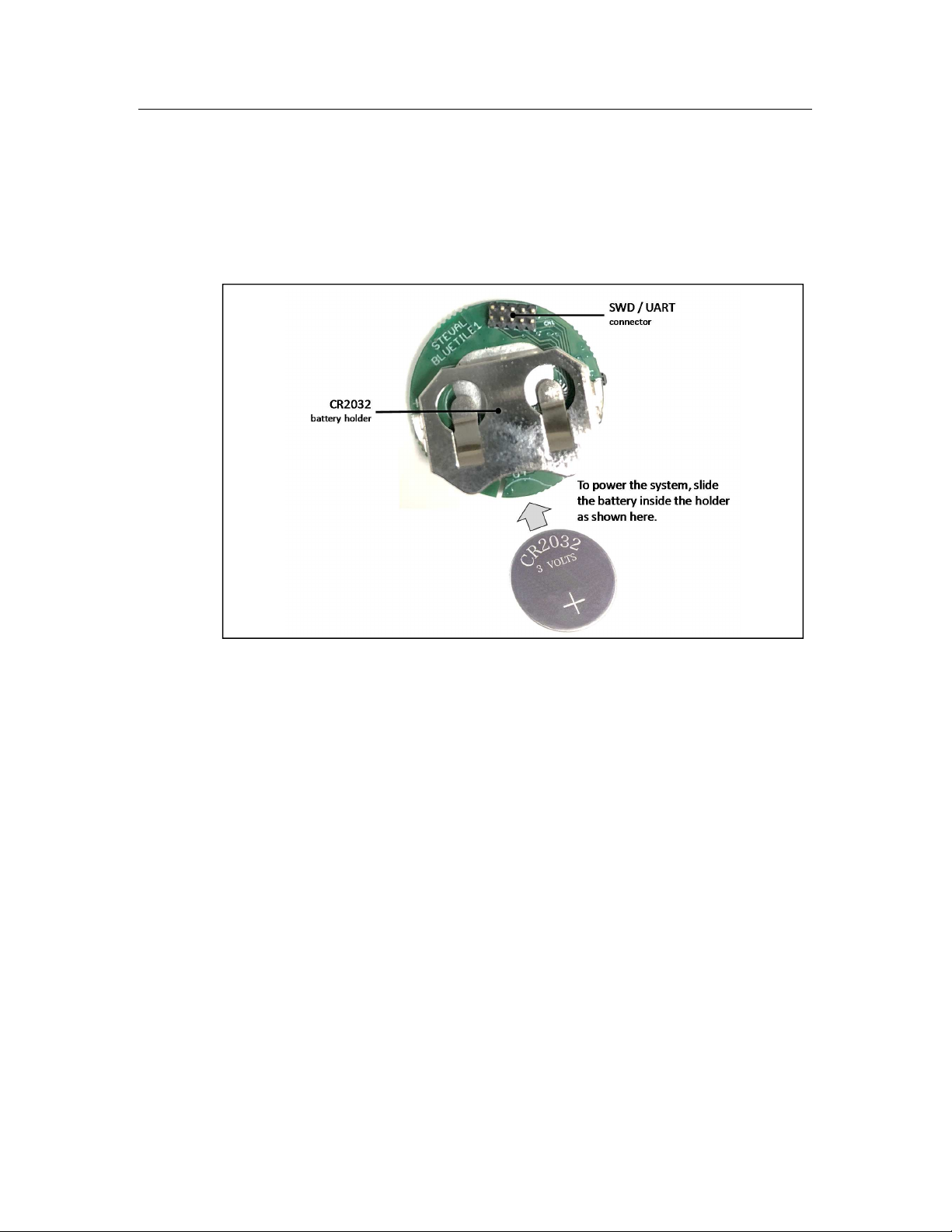
Figure 2. STEVAL-BCN002V1 battery holder and SWD connector
2. Features
The STEVAL-BCN002V1 includes the following components and features:
• BLUENRG-2 Bluetooth low-energy wireless system-on-chip: the device includes
an ultra low-power ARM Cortex-M0 MCU with 256KB Flash and 24KB RAM with
retention, plus an extensive range of enhanced I/O and peripherals (10bit ADC, 2
general purpose 16bit timers, watchdog and RTC, DMA controller, PDM stream
processor, 2 I2C, 1 SPI, 1 UART, up to 26 GPIOs). The embedded Cortex-M0 runs
at 32MHz and supports the radio stack and the user application. The device support
BLE 5.0 stack and proprietary 2.4GHz stack. The device can work with an external
16 or 32MHz crystal, and with an internal 32kHz ring oscillator or an external 32kHz
crystal (which enable lowest power sleep mode). The device includes an integrated
linear regulator and a DC-DC converter (requires an external inductor and enables
lowest power active mode). Power consumption down to 1uA with active BLE stack
(sleep mode); 1.9mA when CPU is running, RAM and Flash on (active mode);
8.3mA TX peak current at -2dBm output power. Up to +8dBm output power, up to
Page 3

UMXXX
96dB link budget.
• BALF-NRG-02D3 50ohm nominal input / conjugate match to BlueNRG transceiver
with integrated harmonic filter.
• LSM6DSO inertial digital module with 3-axis accelerometer and 3-axis
gyroscope. Ultra-low power (0.55mA in combo high-performance mode at the
highest datarate, 6.6kS/s). Configurable free-fall, wakeup, 6D/4D orientation
detection (to support portrait and landscape mode detection), single/double tap
recognition; automatic detection for activity/inactivity and stationary/motion
condition; advanced algorithms for pedometer, step detector and step counter;
significant motion and relative tilt; up to 16 finite state machines (FSM) to process
accelerometer, gyroscope or external sensor data. User selectable full scale of 2,
4, 8 or 16g and 125, 250, 500, 1000 or 2000dps; output data rates from 12.5 to
6600Hz, bandwidth up to 3kHz. The device includes 9KB FIFO buffer for 2 internal
sensors and up to 4 external sensors.
• LIS2MDL ultra low-power high-performance 3-axis magnetic digital sensor, 50
Gauss magnetic dynamic range. Selectable resolution/power trade-off. Output data
rate up to 150Hz. RMS noise down to 3mgauss in high-performance mode with
low-pass filter active. Embedded intrinsic offset cancellation. Embedded registers
for hard-iron offset subtraction. Configurable interrupt.
• LPS22HH ultra-compact piezo-resistive absolute pressure digital sensor, 260-
1260hPa, digital output barometer, full-mold, holed LGA package. The sensing
element, which detects absolute pressure, consists of a suspended membrane
manufactured using a dedicated process developed by ST.
• HTS221 capacitive digital sensor for relative humidity and temperature. The
sensing element consists of a polymer dielectric planar capacitor structure capable
of detecting relative humidity variations and is manufactured using a dedicated ST
process.
• MP34DT05-A compact low-power omnidirectional digital top-port microphone with
a capacitive sensing element; 0.2% THD+N and 64dB signal-to-noise ratio at 1kHz
and 94dBSPL, 0.7% THD+N at 1kHz and 110dBSPL, 122.5dBSPL acoustic
overload point, -26dBFS +/-3dB sensitivity, PDM output (1.2 to 3.25MHz), up to
24kHz bandwidth.
• VL53L1X long distance ranging Time-of-Flight sensor based on ST’s
FlightSense™ technology. 940nm class 1 laser emitter, 16x16 SPAD receiving
array with integrated lens (27deg field of view). Ranging frequency from 1 to 50Hz
Page 4
UMXXX
(repeatability improves at lower data rate, 2.5mm standard deviation with 200msec
measurement); Ranging distance from 4cm to 400cm (under 4cm the device will
detect a target but measurement will not be accurate). Ranging error within 20mm.
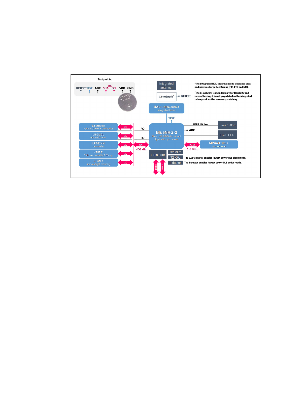
Figure 3. STEVAL-BCN002V1 block diagram
3. System architecture
The BLE sensor node is powered by a coin-cell battery (CR2032). The voltage is NOT
regulated because all sensors and the BlueNRG-2, they can all operate at the voltage range
of the battery. Moreover, the BlueNRG-2 has its own embedded linear power regulator and
switching mode power converter (DC-DC).
POWER SECTION FOR BLUENRG-2
The BlueNRG-2 in active mode can use the embedded linear voltage regulator (LDO) or
the embedded DC-DC converter (DC-DC). The BLE sensor node includes the inductor
needed by the DC-DC converter to enable the lowest power consumption in active mode:
• Active mode, CPU Flash and RAM on, LDO regulator: RX 14.5mA at 3V, TX
17.2mA when output power is +2dBm, range is 12-28.8mA when output is -14 to
+8dBm
• Active mode, CPU Flash and RAM on, DC-DC converter: RX 7.7mA at 3V, TX
9mA at 3V when output power is +2dBm, range is 6.6-15.1mA when output is -14
to +8dBm
The BlueNRG-2 in sleep mode can use the internal 32kHz ring oscillator (RO) or an external
32kHz crystal oscillator (XO). The BLE sensor node includes the 32kHz crystal oscillator
Page 5

UMXXX
to enable the lowest power consumption in sleep mode:
• Sleep mode, 32kHz RO (Ring oscillator), 24kB RAM retention: 2.1uA at 3V
• Sleep mode, 32kHz XO (Crystal oscillator), 24kB RAM retention: 0.9uA at 3V
RADIO FREQUENCY SECTION
The Radio Frequency section of the BLE sensor node includes three elements:
• The first element is BALF-NRG-02D3, an ultra-miniature balun which integrates
matching network and harmonics filter.
• The second element is a Π-network which provides the flexibility to get additional
filtering and also provides access points for testing. This network is not populated
as the integrated balun provides the necessary matching.
• The third element is the SMD 2.4GHz antenna which needs a specific clearance
area on the PCB and specific passives for perfect tuning (FT1, FT2 and MT).
MEMS SENSOR SECTION
The Sensor section of the BLE sensor node includes inertial and environmental MEMS
sensors connected to BlueNRG-2 by means of an I2C bus operated at 400kHz.
The MEMS microphone is connected to BlueNRG-2 using a dedicated line to transfer the
PDM (Pulse Density Modulated) stream at 1.6MHz. The PDM stream is converted to PCM
(Pulse Coded Modulation) by the integrated digital filter included in the ADC block on
BlueNRG-2.
All sensors can generate interrupts, but in the BLE sensor node, only two interrupt pins are
connected to BlueNRG-2 using dedicated and independent lines: the interrupt from the
LIS2MDL magnetometer and the interrupt from the LSM6DSO accelerometer and
gyroscope.
• The LIS2MDL magnetometer interrupt line is only push-pull and must have its own
independent line. The interrupt pin of this sensor is connected to BlueNRG-2 to
enable applications such as “reed-switch” (switch activated by an external magnet).
• The LSM6DSO smart accelerometer and gyroscope interrupt pin is an input at boot.
It has an internal pull-down. If the pin is low at boot, the I2C interface is selected,
otherwise the I3C interface is selected. The pin can be reconfigured as open-drain
but the external pull-up would cause an additional power consumption. The
interrupt pin of this sensor is connected to BlueNRG-2 to fully exploit the “smart”
embedded processing (single/double tap recognition, free-fall, wakeup,
portrait/landscape, 6D/4D orientation detection; activity/inactivity, stationary/motion
Page 6

UMXXX
detection; pedometer, step detector and step counter; up to 16 finite state machines
to process
• The LPS22HH barometer interrupt pin is the same as for LSM6DSO: it is an input
pin at boot and must be low so that I2C interface is activated. It can be configured
as push-pull or open-drain after boot. The interrupt pin of this sensor is not
connected to BlueNRG-2.
• The HTS221 relative humidity and temperature interrupt pin is push-pull at boot and
can be reconfigured as open-drain after boot. The interrupt pin of this sensor is not
connected to BlueNRG-2.
• The VL53L1X time-of-flight proximity interrupt line is only open-drain and would
require an external pull-up. The interrupt pin of this sensor is not connected to
BlueNRG-2.
From the application point of view, the dynamic of the environmental parameters is very
slow. Therefore, an interrupt need not be used. The application can wake-up on a regular
basis, every few seconds, perform one-shot measurements with the LPS22HH barometer
or HTS221 relative humidity and temperature sensor, and trigger the corresponding action
if specific conditions are met.
Also, from the application point of view, it is not convenient to keep the VL53L1X proximity
time-of-flight sensor active, waiting for a gesture and a corresponding wake-up interrupt.
The power consumption or the latency would be too high. The power consumption of
VL53L1X ranges from 0.5mA for 1Hz measurements, up to 7mA for 10Hz measurements.
4. BlueNRG-2 features
BlueNRG-2 integrates a Bluetooth Low Energy radio (BLE), an ARM Cortex-M0 core,
12+12kB of RAM, 256kB of Flash memory and several peripherals: SPI (max 1MHz in slave
mode, 8MHz in master mode), 2x I2C (standard 100kHz or fast 400kHz), and UART
interfaces; 2x multi-function timer (MFT), DMA controller, RTC and watchdog, ADC with
PDM stream processor.
The public key cryptography (PKA) and random number generator (RNG) are reserved for
the BLE protocol stack, however the user application can also read the RNG.
The ADC features are: 10-bit, single or continuous acquisition at max 1MHz sampling
frequency, 2x single ended or 1x differential signal (ADC1 and ADC2 pins), embedded
channels for temperature and battery voltage sensing, embedded digital filter with down
sampling. The embedded digital filter can be used to process the PDM stream coming from
a digital MEMS microphone (1.6MHz or 0.8MHz) and convert it to audio PCM (8kHz to
50kHz when 1.6MHz clock is used for the microphone). The BlueNRG-2 sensor node
Page 7

UMXXX
does exploit the embedded digital filter of the ADC peripheral for PDM to PCM
conversion when reading the PDM output of the MEMS microphone MP34DT05-A.
The low-speed clock is used in low-power mode and can be supplied by the internal RC
oscillator or by an external crystal (32kHz +/-50ppm). The high-speed clock is supplied by
a fast-starting internal RC oscillator (16MHz) while the external crystal is starting up. The
high-speed external crystal (16 or 32MHz) is strictly required to enable the BLE radio.
In order to support the highest computational load, the 32MHz XO must be used. When
32MHz XO is used, the Cortex-M0, the DMA and the APB tree run at 32MHz while the rest
of the clock tree runs at 16MHz. When 16MHz XO is used, the Cortex-M0 and all the clock
tree runs at 16MHz.
BlueNRG-2 states
• Preactive (reachable from Reset, Standby or Sleep, goes to Active): after power-
on-reset, all digital power supplies are stable; internal 16MHz and 32kHz RC
oscillators are used.
• Active (reachable only from Preactive): the external high-frequency crystal is used
(16MHz +/-50ppm or 32MHz) to enable BLE communication; the internal 16MHz
RC oscillator is switched off; the higher the accuracy of the crystal, the lower the
power consumption is; the BlueNRG-2 sensor node uses a 32MHz +/-10ppm
crystal. In active mode the radio can be activated for transmission (TX) or reception
(RX). This is the state used by BlueNRG-2 when the user application is
running or there is a BLE event to serve.
• Standby (reachable from Active, can go to Preactive): RAM retention is used (12 or
24kB); 5 different GPIOs can be used to wake-up (IO9, IO10, IO11 which have an
internal pull-up, and IO12, IO13 which require an external drive); the BlueNRG-2
sensor node uses IO11 connected to the user button, IO12 connected to the
interrupt pin of LIS2MDL magnetometer, and IO13 connected to the interrupt pin of
of LSM6DSO accelerometer and gyroscope. The wake-up time is typically 200us.
• Sleep (reachable from Active, can go to Preactive): RAM retention is used (12 or
24kB); the low-frequency oscillator is switched on to serve periodic BLE connection
events; as in Standby state, 5 different GPIOs can also be used to wake-up. This
is the state used by the BlueNRG-2 tile to save power when the user
application is not running and the device is waiting for a BLE event to serve.
BLE FIRMWARE STACK AND MEMORY MAP
Program memory, data memory, registers and I/O ports are organized in a linear 32-bit
address space.
Page 8

UMXXX
• The SRAM is divided in two banks
o 12KB from 0x2000_0000 to 0x2000_2FFF, retention always-on
o 12KB from 0x2000_3000 to 0x2000_5FFF, retention optional
o The FULL BLE stack needs 9.6KB of SRAM; see below for FULL BLE stack
features.
o The BASIC BLE stack needs 0.0KB of SRAM; see below for BASIC BLE
stack features.
• The Flash is 256KB from 0x1004_0000 to 0x1007_FFFF
o The FULL BLE stack needs 77KB, leaving 179KB for the user application;
the FULL BLE stack will support concurrent peripheral and central roles
(N=0,1,2 connections to other centrals and 8-N connections to other
peripherals), LE secure connections, controller privacy, extended data
length.
o The BASIC BLE stack needs 58KB, leaving 198KB for the user
application; the BASIC BLE stack will support only the peripheral role (1
connection to a central), only legacy security, no controller privacy and no
extended data length.
o The OTA manager to enable over-the-air firmware updates adds 10KB to
the size of the BLE stack. The OTA manager may be independent of the
user application, or it may be embedded in the user application.
When the OTA manager is independent of the user application, the Flash is divided in two
section. The first relatively small section is dedicated to the OTA application; the size is the
sum of BLE stack size and OTA manager size. The second large section is dedicated to
the user application and is made of the rest of the Flash. This has the advantage of leaving
the largest space to the user application, but it has the disadvantage that there is no
application to run if the update is not completed successfully.
When the OTA manager is embedded in the user application, the Flash is divided in three
sections. The first section is dedicated to the current old application; the size is the sum of
BLE stack size, OTA manager size and user application size. The second section is
dedicated to the new updated application; the size is the same as the first section. The third
very small section is dedicated to the reset application; the reset application decides which
application to run after boot, depending on what is available and valid in the first two
sections. This has the advantage that even if the update is not completed successfully,
there will always be a valid old application to run. The disadvantage is that the space
available for the user application is less than half the size of the Flash. Note that after a
Page 9

UMXXX
successful update, the new application can be copied over the old application or the role of
the first two sections can be exchanged.
5. Inertial MEMS sensors features
Each sensor is made of two parts: the first is the Micro Electro Mechanical system (MEMS)
which includes the sensing element; the second is the dedicated ASIC with the analog
acquisition chain, the analog-to-digital converter (ADC), and the dedicated digital signal
processing (DSP) and control logic.
LSM6DSO INTERRUPT GENERATION
The LSM6DSO delivers best-in-class motion sensing that can detect orientation and
gestures in order to empower application developers and consumers with features and
capabilities that are more sophisticated than simply orienting their devices to portrait and
landscape mode.
The event-detection interrupts enable efficient and reliable motion tracking and contextual
awareness, implementing hardware recognition of free-fall events, 6D orientation, click and
double-click sensing, activity or inactivity, stationary/motion detection and wakeup events.
• Free-fall event: when the device is in free fall, acceleration data is near zero. The
user can define a threshold and a duration. The free-fall event is detected if data
from all enabled axis is under the programmed threshold for the minimum
programmed duration.
• Wake-up event: the user can choose to one of the following: high-pass filtered data,
the output of the slope detection filter (the slope is the computed as the difference
of consecutive samples, divided by two), low-pass filtered data summed with a
programmable offset (independent for each axis), or unfiltered data summed with
the programmable offset; the low/high-pass filters are configurable; the wake-up
event is detected if the filtered data from any of the enabled axis is over the
threshold for the minimum programmed duration.
• 6D/4D orientation event: the user can choose to use unfiltered data or low-pass
filtered data (the low-pass filter is the same as mentioned above); a specific 6D
orientation is detected when one axis (positive or negative) is above the
programmed threshold, while the other two are below the threshold, for the
minimum programmed duration; 4D is a subset of 6D: in this configuration the Z
axis is not used.
• Single/Double tap event: the single tap event is detected when the output of the
slope detection filter exceeds the programmed threshold and then returns below it
within the programmed “shock” time window (the high-pass filter is the same as
Page 10

UMXXX
mentioned above); the double tap event is detected when a first tap is detected,
and a second tap is detected after the programmed “quiet” time window but before
the maximum “duration” time window; for a reliable detection of short duration shock
events, it is suggested to configure the device to use a high sampling rate (e.g.
400Hz). If more than one axis is enabled, and they are over their respective
threshold, the highest priority axis is used; the priority can be configured.
• Activity/Inactivity event: uses the same data as selected for the wake-up event; if
inactivity is detected (data below the programmed threshold for the programmed
duration), the device automatically goes to low-power mode and reduces the
accelerometer sampling rate down to 12.5Hz to minimize power consumption; if
activity is detected (wake-up event) the device automatically returns to the
programmed accelerometer operating mode and sampling rate. This feature may
be configured to put the gyroscope in power-down or sleep mode when the
accelerometer is in low-power mode.
• Stationary/Motion event: is a particular case of Activity/Inactivity event; event
detection is the same but the device does not change in power mode or sampling
rate.
Single/double tap recognition may be used to enable user interaction in addition to the use
of the button present in the BlueNRG-2 sensor node. The on-board LED can be used to
give feedback to the user.
LSM6DSO INTERRUPT GENERATION AND ADVANCED FUNCTIONS
Specific digital processing blocks enable advanced functions and algorithms: pedometer
functions with step detector and step counter, tilt detection, significant motion detection.
These functions require the output data rate to be 26 Hz or higher.
• Pedometer functions: step detector and step counter. An interrupt is generated
whenever a step is detected and the corresponding counter is incremented by 1
(max value is 65535). Optionally the interrupt can be generated only if at least one
step is detected in a configurable time interval. In order to avoid false detections, N
consecutive steps must be detected before the first interrupt is generated (debounce functionality), when this happens the counter is incremented by N. the
parameter N is configurable. Two additional blocks can be enabled to enhance the
rejection of false-positives: the first block enable the step detection only is statistical
data matches the walking pattern; the second block adapts the embedded
algorithm to slow pace walking patterns. STMicroelectronics provides the software
tools to generate specific pedometer configurations based on data logs. The step
counter is not reset to 0 when the accelerometer is configured to power-down
Page 11

UMXXX
mode, or the step counter is disabled or re-initialized. The step counter can be reset
explicitly by the user application.
• Significant motion detection: this function generates an interrupt when there is a
change in user location, computed by integrating accelerometer data.
• Relative tilt detection: this function generates an interrupt when there is a change
in the tilt of the device. The interrupt is generated when the change in tilt exceeds
35 degrees. The reference start position is set when the detection logic is enabled
and it is reset when the interrupt is generated. The detection logic requires a 2
second settling time after it is enabled or re-initialized.
LSM6DSO FINITE STATE MACHINES
The LSM6DSO can have up to 16 FSM running concurrently. Each FSM is composed by a
sequence of instructions where each instruction is an immediate action (parameter setting,
interrupt generation, etc) or a RESET-NEXT condition. If the reset condition is satisfied, the
FSM goes back to the programmed reset point; if the next condition is satisfied, the FSM
moves to the next instruction; otherwise the RESET- NEXT conditions are re-tested. Each
FSM can be configured independently. FSM data can be one of the following:
accelerometer, gyroscope, integrated gyroscope or external sensor data. Data can be
decimated. Data vector is made of X, Y, Z values and a vector norm V (square root of sum
of squares). Each FSM has 3 different 8-bit masks to enable tests on positive and negative
values of X, Y, Z and V; also, each FSM has 3 different thresholds and 1 programmable
hysteresis value which is automatically added or subtracted to the selected threshold based
on the test condition; finally, each FSM has 4 different counters/timers to manage events’
durations.
LSM6DSO SMART FIFO BUFFER
The LSM6DSO accelerometer has a first-in first-out data buffer (FIFO) which can store up
to 3KB of data: 512 words of 7 bytes each; the first byte is a tag followed by six bytes of
data. The tag in the word drives the decoding. The tag includes a parity bit for validation.
The data source can be any combination of the following: the accelerometer, gyroscope,
up to 4 external sensors, embedded temperature sensor, timestamp counter and the
pedometer step counter. The data rates can be set independently for each source.
For the accelerometer: the user can choose to store high-pass filtered data, the output of
the slope detection filter, low-pass filtered data or unfiltered data summed with an optional
and programmable offset (independent for each axis); the low/high-pass filters are
configurable.
For the gyroscope: the user can choose to enable a first optional high-pass filter, and a
second optional and programmable low-pass filter.
Page 12

UMXXX
In order to maximize the amount of data stored in the FIFO, the user can enable a lossless
DPCM compression algorithm for the accelerometer and/or the gyroscope data. When
DPCM compression is enabled, it is also possible to select when DPCM is reset by storing
uncompressed data in the FIFO (never, or every 8, 16 or 32 words); this is useful when the
FIFO is used as a circular buffer (Continuous mode, see below) and words may be
overwritten: DPCM decoding of the current data word is possible only if previous data words
can be read from the FIFO, back to the point where an uncompressed data word is stored.
The DPCM compression works on 3 data words (sampled at time t, t-1 and t-2) and
introduces a latency of 2 data words. The compression factor depends on the difference
between a data word and the previous data word. When it is disabled, the compression
buffer will be flushed and the output will be the non-compressed data word at time t-2, then
data word at time t-1 and data words at current time t thereafter (tag “NC_T_2”, “NC_T_1”,
and “NC”). When it is enabled, the first output will be the non-compressed data word at time
t-2 (tag “NC_T_2”) so that the decoder has a reference to start decoding; the next outputs
depend on the difference D2 between data word at time t-2 and the previous decoded word,
difference D1 between data word at time t-1 and t-2, and difference D0 between data word
at time t and t-1:
• If any difference in D2 exceeds 128LSB on any axis, the uncompressed data word
at time t-2 is written to the FIFO by storing the 16-bits signed value of each axis
(low and high bytes for X, Y and Z: XL XH YL YH ZL ZH, for a total of 6 bytes); tag
“NC_T_2”.
• If any difference in D2 and D1 exceeds 16LSB but is within 128LSB for all axis, a
2x compression ratio is applied by storing the 8-bit signed difference to reconstruct
2 data values for each axis at time t-1 and t-2 (D1x D1y D1z, then D2x D2y D2z,
for a total of 6 bytes); tag “2xC”. The data at time t-2 is reconstructed by summing
D2 to the previous decoded data word. The data at time t-1 is reconstructed by
summing D1 to the data at time t-2 just reconstructed.
• If all differences in D2, D1 and D0 are within 16LSB for all axis, a 3x compression
ratio is applied by storing the 5-bit signed difference to reconstruct 3 data values
for each axis at time t, t-1 and t-2 (D0x D0y D0z and a dummy bit to make 16bits,
then D1x D1y D1z and a dummy bit, then D2x D2y D2z and a dummy bit, for a total
of 6 bytes); tag “3xC”. The data at time t-2 is reconstructed by summing D2 to the
previous decoded data word. The data at time t-1 is reconstructed by summing D1
to the data at time t-2 just reconstructed. The data at time t is reconstructed by
summing D0 to the data at time t-1 just reconstructed.
Interrupts can be generated when the FIFO buffer stores a given number of samples
Page 13

UMXXX
(FIFO threshold level), or when it is full, or when it overflows (overrun). The FIFO can
work in the following modes:
• Bypass mode: the FIFO buffer is disabled and cleared.
• FIFO mode: the FIFO buffer collects data until it is full, then stops.
• Continuous mode: the FIFO buffer collects data continuously, when it is full oldest
samples are overwritten as in a circular buffer. The host microcontroller may read
the data before it is overwritten thanks to the FIFO full and FIFO threshold level
interrupts.
• Continuous-to-FIFO mode: the FIFO buffer collects data continuously but switch to
FIFO mode as soon as the selected interrupt occurs. This mode is especially useful
to capture data before and after a specific event.
• Bypass-to-Continuous mode: the FIFO buffer is disabled but switch to continuous
mode as soon as the selected interrupt occurs. This mode is useful to capture data
after an event has occurred.
• Bypass-to-FIFO mode: the FIFO buffer is disabled but switch to FIFO mode as soon
as the selected interrupt occurs. This mode is useful to capture data after an event
has occurred. FIFO is filled and then data collection stops.
LIS2MDL DYNAMIC RANGE, RESOLUTION AND ACCURACY
The LIS2MDL is a 3D digital magnetometer. The magnetic field dynamic range is +/-50
Gauss (reduced to +/-25 Gauss if the magnetic field is not aligned with one of the axis); well
above the earth magnetic field level (which is typically in the range of 0.25 to 0.65 Gauss).
However, the resolution and accuracy is also high: the output is 16 bits (1.5 mgauss/LSB
+/-7%), the RMS noise level in high-performance mode is 3 mgauss (2LSB). This enables
applications such as accurate e-compass orientation estimation as well as distance
measurements from a reference magnet (in its simplest form: the magnetometer can
emulate a Reed-switch, a magnetically activated switch).
The LIS2MDL magnetometer can perform a single-shot measurement and then return to
power-down mode, or it can operate in continuous mode with a programmable sampling
rate (10, 20, 50 or 100 Hz). Single-shot measurements can be done at max 100 Hz in highperformance mode, or max 150 Hz in low-power mode. In low-power mode the power
consumption is reduced to 25%, while in high-performance mode the RMS noise is halved.
An optional low-pass filter can be activated to further reduce RMS noise, without increasing
the power consumption, the bandwidth in this case is reduced from output data rate ODR/2
down to ODR/4.
LIS2MDL INTRINSIC OFFSET AUTOMATIC CANCELLATION
Page 14

UMXXX
The LIS2MDL is based on AMR technology (anisotropic magneto-resistive): a set pulse is
needed to set an initial operating condition; a reset pulse may be used to enable the
compensation of the intrinsic magnetic offset.
• If intrinsic offset compensation is disabled, there is no reset pulse. The set pulse
can be generated at power-on only (Set_FREQ=1), or every 64 measurements
(Set_FREQ=0).
• If intrinsic offset compensation is enabled, set and reset pulses are generated
alternately on consecutive samples. After the set pulse, the measured output is
magnetic field H + offset; after the reset pulse, the measured output is H – offset
o In continuous mode, the device will automatically average consecutive
measurements to compensate for the offset, the output will be equal to the
magnetic field H: output = [( H+offset) + (H-offset)]/2 = H.
o In single-shot mode, the host microcontroller has to perform the average of
two consecutive measurements. The averaged measurements must be
near in time for the compensation to be effective.
When intrinsic offset compensation is done, the residual offset is in the range of +/-60
mgauss, and the dependency on temperature is +/-0.3 mgauss/degC.
LIS2MDL EXTRINSIC OFFSET (HARD IRON) COMPENSATION
Hard-iron distortion is a constant offset added to the magnetic field to be measured. Hardiron distortion may be caused by near-by ferromagnetic materials or high currents. This
offset can be computed by the host microcontroller by analyzing the output of the
magnetometer (see DT0059 on ellipsoid or sphere fitting, also see MotionMC software
library in X-CUBE-MEMS1 software expansion on st.com). When it is available, this offset
can be programmed in specific registers (OFFSET_X_REG_H/L, OFFSET_Y_REG_H/L,
OFFSET_Z_REG_H/L) so that it is automatically subtracted by LIS2MDL.
LIS2MDL INTERRUPT GENERATION
The LIS2MDL magnetometer sensor can be configured to generate interrupt when output
data (before or after the subtraction of hard-iron offset) exceeds a programmed threshold
(INT_THS_H/L_REG) in the positive or negative direction. Comparisons can be enabled
independently for each axis (XIEN, YIEN, ZIEN flags). When the output data is above the
positive threshold, the corresponding flag is set (P_TH_S_X/Y/Z). When the output data is
below the negative threshold, the corresponding flag is se t(N_TH_S_X/Y/Z).
A specific interrupt can be generated if there is a measurement range overflow at the
internal ADC.
Page 15

UMXXX
6. Environmental MEMS sensors features
LPS22HH ACQUISITION CHAIN
The LPS22HH pressure sensor can perform a one-shot measurement and then return to
power-down mode, or it can operate in continuous mode with a programmable sampling
rate (1, 10, 25, 50, 75, 100 or 200Hz). The measurements can be taken in normal low-noise
mode, or in low-power mode to minimize current consumption. When continuous mode is
selected, low-noise mode is not available at 100 and 200Hz. In all cases, an optional lowpass filter can be enabled with a programmable cutoff frequency to reduce the noise level
(the bandwidth is reduced from output data rate ODR/2 down to ODR/9 or ODR/20). The
low-pass filter is reset when it is enabled; after reset, a specific settling time is required
before the first correct sample on output (9 or 20 samples must be discarded, respectively).
Two programmable offsets can be subtracted from measured data:
• First, offset compensation (always): the offset measured with one-point calibration
(OPC) can be stored in specific registers (RPDS) and then subtracted from
subsequent measurements (OPC-compensated data = data – RPDS*256). The
low-pass filter, if enabled, will filter OPC-compensated data. Un/filtered OPCcompensated data is stored in the FIFO.
• Second, auto-zero mode (optional): the offset-compensated (and possibly filtered)
pressure measurements is stored in specific registers (REF_P) when auto-zero is
enabled (AUTOZERO or AUTOREFP set to 1) and then it is subtracted from
subsequent measurements (AZ-compensated data = data – REF_P). Un/filtered
OPC-compensated data or AZ-compensated is stored in output registers.
LPS22HH INTERRUPT GENERATION AND FIFO BUFFER
The LPS22HH pressure sensor can be configured to generate interrupt events related to
pressure acquisitions (see below) and FIFO status (watermark reached, full, overrun).
The interrupt can be generated when a new pressure or temperature sample is available;
or when the AZ-compensated data exceeds a programmed threshold (THS_P) in the
positive (PHE flag enables the comparison with +THS_P) or negative direction (PLE flag
enables the comparison with –THS_P). There are three configurations:
• AUTOZERO=0 and AUTOREFP=0: interrupt logic is disabled; un/filtered OPC-
compensated data goes to FIFO and output registers.
• AUTOZERO=1: interrupt logic is enabled; REF_P is set when interrupt is enabled;
AZ-compensated data goes to the interrupt logic and to the output registers, while
un/filtered OPC-compensated data goes to FIFO.
• AUTOREFP=1: interrupt logic is enabled; REF_P is set when interrupt is enabled;
Page 16

UMXXX
AZ-compensated data goes to interrupt logic, while un/filtered OPC-compensated
data goes to FIFO and output registers.
The FIFO buffer can store up to 128 pressure samples (24 bit each) and 128 temperature
samples (16 bit each). FIFO depth can be limited by stopping at the programmable
watermark level. The FIFO can work in the following modes:
• Bypass mode: the FIFO buffer is disabled and cleared.
• FIFO mode: the FIFO buffer collects data until it is full or until the programmed
watermark level is reached, then stops.
• Continuous (or Dynamic Stream) mode: the FIFO buffer collects data continuously,
when it is full or the watermark level is reached, oldest samples are overwritten as
in a circular buffer. The host microcontroller may read the data before it is
overwritten thanks to the FIFO full and FIFO watermark level interrupts.
• Continuous (Dynamic Stream)-to-FIFO mode: the FIFO buffer collects data
continuously but switch to FIFO mode as soon as the selected interrupt occurs.
This mode is especially useful to capture data before and after a specific event.
• Bypass-to-Continuous (Dynamic Stream) mode: the FIFO buffer is disabled but
switch to stream mode as soon as the selected interrupt occurs. This mode is useful
to capture data after an event has occurred.
• Bypass-to-FIFO mode: the FIFO buffer is disabled but switch to FIFO mode as soon
as the selected interrupt occurs. This mode is useful to capture data after an event
has occurred.
LPS22HH vs HTS221 AMBIENT TEMPERATURE MEASUREMENT
The temperature sensor in LPS22HH is designed and used to compensate for temperature
effects in ambient pressure measurements. On the opposite, the temperature sensor in
HTS221 is designed and characterized for ambient temperature measurements.
In the BlueNRG-2 sensor node the ambient temperature is read from HTS221 because of
its higher accuracy and larger range with respect to LPS22HH. If the application needs a
high data rate (above 12.5 Hz), one can use the LPS22HH temperature sensor.
Here is a summary of the characteristics of the embedded temperature sensor:
• LPS22HH: temperature sensor operating range from -40 to +85 Celsius degrees,
sensitivity 100 LSB/degC, temperature absolute accuracy +/-1.5degC (from 0 to 80
Celsius degrees); data rate: 1, 10, 25, 50, 75, 100, 200 Hz.
• HTS221: temperature sensor operating range from -40 to +120 Celsius degrees,
sensitivity 64 LSB/degC, temperature absolute accuracy +/-1degC (from 0 to 60
Page 17

UMXXX
Celsius degrees), +/-0.5degC (from 15 to 40 Celsius degrees); data rate 1, 7 or
12.5 Hz. Response time 15 s (time to 63%). Long term drift 0.05degC/year.
HTS221 ACQUISITION CHAIN
All components on the board, the MEMS sensors, the BlueNRG-2 processor, have an
embedded temperature sensor. These temperature sensors have been design to enable
the measurement of the temperature of the silicon, not the ambient temperature. On the
opposite, the temperature sensor embedded in HTS221 has the physical properties and the
accuracy required by the measurement of the ambient temperature.
The raw output of the humidity acquisition chain is stored in two 8bit registers
(HUMIDITY_OUT_H and _L) which must be concatenated to get a 16bit two’s complement
value (H_OUT). The raw output is already temperature-compensated. Calibrations
coefficients to go from raw humidity output to Relative Humidity (RH) are stored in the
device. Factory calibration is performed at two different humidity levels and one
temperature. This is the sequence to compute RH:
1. First true RH during calibration: H0_rH_x2, set RH0 = H0_rH_x2 / 2
2. Second true RH during calibration: H1_rH_x2, set RH1 = H0_rH_x2 / 2
3. First raw H output during calibration: H0_T0_OUT, set H0 = H0_T0_OUT
4. Second raw H output during calib.: H1_T0_OUT, set H1 = H1_T0_OUT
5. Current raw H output: H_OUT, set H = H_OUT
6. Current RH% by linear interpolation: RH = RH0 + (RH1-RH0) * (H-H0)/(H1-H0)
The raw output of the temperature acquisition chain is stored in two 8bit registers
(TEMP_OUT_H and _L) which must be concatenated to get a 16bit two’s complement value
(T_OUT). Calibration coefficients to go from raw temperature output to Temperature in
Celsius degrees are stored in the device. Factory calibration is performed at two different
temperatures. This is the sequence to compute Temperature in Celsius degrees:
1. MSB of true temperatures during calibration: T1T0MSB,
• set MSB1 = T1T0MSB & 0x03, MSB0 = T1T0MSB/4
2. First true T in Celsius deg. (two’s comp): T0_degC_x8,
• set T0degC = (T0_degC_x8 + MSB0*256)/8
3. Second true T in Celsius deg. (two’s comp): T1_degC_x8,
• set T1degC = (T1_degC_x8 + MSB1*256)/8
4. First raw T output during calibration: T0_OUT, set T0 = T0_OUT
Page 18

UMXXX
5. Second raw T output during calibration: T1_OUT, set T1 = T1_OUT
6. Current raw T output during calibration: T_OUT, set T = T_OUT
7. Current Temperature in Celsius degrees:
• T = T0deg + (T1deg-T0deg) * (T-T0)/(T1-T0)
HTS221 SYSTEM INTEGRATION
To get reliable and consistent measurements, the system design should maximize sensor
exposure to the external environment while minimizing error sources. See also application
note AN4722.
• Mechanical design: if there is one vent hole in the BlueNRG-2 sensor node housing, the
hole diameter should be maximized and the dead volume enclosed should be minimized;
two or multiple vent holes are preferable, in order to create a laminar airflow and minimize
the response time. Materials that absorb humidity should be avoided.
• Mechanical stress: any mechanical force applied directly or indirectly to the sensor may
affect the output. The BlueNRG-2 sensor node board should not be flexed/curved.
• Heat convection or temperature gradients on the board may affect the sensor Metal lines
and planes, such as the ground plane, should be kept far from the sensor. Milled slits further
increase decoupling. Insulation may be required to isolate the BlueNRG-2 sensor node from
convective and conducted heat.
• Light exposure may induce a change in temperature and humidity.
The internal heating element can effectively be used to speed up sensor recovery in case
of condensation. The heater control is not automatic; it must be switched on/off by the
firmware running on the host microcontroller. Humidity and temperature data should not be
read during the heating cycle. Valid data can only be read once the heater has been turned
off, after the completion of the heating cycle.
BlueNRG-2 sensor node has been designed for ultra-low power operation to enable a very
long battery life (3-10 years on a typical CR2032 coin battery, depending on the application).
Power and heat generated on-board is therefore very limited. Possible sources of
conducted heat, such as the BlueNRG-2 and the LED, have been placed as far as possible
from MEMS sensors to increase the accuracy of the measurements. Milled slits have been
used to further isolate HTS221 temperature sensor from neighboring components.
7. Digital MEMS microphone features
A MEMS microphone is a dual-die device. The first die is a MEMS (micro electromechanical
system) and it is basically a silicon capacitor; the second die is an ASIC (application specific
integrated circuit) that converts the polarized MEMS capacitance in an analog or digital
Page 19

UMXXX
PDM modulated output. The sound inlet (port) can be at the top or at the bottom of the
package. Top-port microphones are easier to assemble (sound port can be easily protected
during assembly), but SNR and frequency response are not optimal; bottom-port
microphone are more difficult to use (soldering process must be very careful to avoid dust
or soldering paste enter the sound port, a precisely aligned hole must be carved in the PCB,
PCB thickness does matter), but SNR and frequency response are optimal.
The MP34DT05-A is an omnidirectional top-port digital microphone: the acoustic overload
point (AOP) is at 122.5 dBSPL and corresponds to 0dBFS (100% of digital Full Scale); the
reference audio at 1kHz and 94dBSPL corresponds to -26dBFS +/-3dB (5% of FS); the Aweighted SNR is 64dB. A-weighting gives less weight to frequencies below 1kHz and above
10kHz, as the sensitivity of the human ear is reduced at those frequencies; on the opposite,
slightly more weight is given to frequencies around 3kHz where human ear has its peak
sensitivity. Roughly speaking, the equivalent input noise floor will be at 94-64 = 30 dBSPL,
which corresponds to -26-64 = -90 dBFS (0.003% of FS). The total harmonic distortion plus
noise THD+N at 94 dBSPL is 0.2%, at 110 dBSPL is 0.7%, at 120 dBSPL is 6%, best in
class.enabling the highest audio fidelity.
The frequency response is practically flat from 100 Hz to 5kHz, up to +0.5dB at 20kHz. This
is especially important, even if mic sensitivity variations are estimated and compensated in
real time, to maximize the performance of beamforming applications, when the output of at
least two microphones is combined to achieve some directionality and reject noise coming
from specific directions (see AcousticBF library in X-CUBE-MEMSMIC1 software expansion
on st.com).
PDM to PCM conversion
The output of the digital MEMS microphone is a bit stream at a rate equal to the clock given
to the microphone (1.2 to 3.25 MHz, 1.6 MHz is used on the BlueNRG-2 sensor node). The
frequency of ones is proportional to the sound pressure level; this is known as PulseDensity-Modulation (PDM). However, audio is usually represented by words with at least
16 bits, at a rate equal or greater than twice the max audio frequency, typically 16, 24, 48
kHz; this is known as Pulse-Coded-Modulation (PCM).
The PDM-to-PCM conversion can be done by low-pass filtering; in its simplest form, this is
equivalent to averaging, or counting the number of ones in a time interval, equivalent to the
sampling time of the PCM word. The conversion can be done in software (see PDM2PCM
library in X-CUBE-MEMSMIC1 software expansion on st.com, AN3998 PDM audio software
decoding) or in hardware (see AN4957 DFSDM filters on STM32 microcontrollers). In the
BlueNRG-2 sensor node the conversion is done in hardware by a dedicated block in the
ADC peripheral.
Page 20

UMXXX
8. Time-of-Flight sensor features
The VL53L1X is a state-of-the-art laser-ranging sensor in a miniaturized package. It
integrates a 940nm Class 1 vertical-cavity surface-emitting laser (VCSEL), a receiving
16x16 array of single-photon-avalanche-detectors (SPAD), physical infrared filters and
optics to achieve the best ranging performance. Unlike conventional ranging sensor,
VL53L1X measures the time-of-flight of photons emitted by the laser and reflected back by
the target. This allows an absolute distance measurement, which is independent of target
color or reflectance.
The field-of-view (FoV) is programmable from 15 to 27 degrees. When the full array of
SPAD is used the FoV is 27 deg; the FoV is reduced by selecting a subset, known as regionof-interest (ROI), in the SPAD array: 4x4 to 16x16 ROI size can be selected; the position of
the ROI in the array can also be set, in order to orient the FoV cone in a specific direction.
Reported values from the sensor are the ranging distance in mm, the return signal rate and
the ambient signal rate (kilo-count-per-second per SPAD, kcps), and the range status.
CALIBRATION FOR BEST PERFORMANCE
To get the best performance, it is advised to run calibration functions at least once after
assembly is completed. Calibration data must be stored in the host microcontroller and
loaded in VL53L1X at each startup.
• RefSPAD calibration (if used must be first called) should be used to optimize device
dynamic and accuracy: SPAD cells are classified as non-attenuated, attenuated by
5 or attenuated by 10; then SPAD are selected to avoid internal signal saturation.
This part-to-part value is computed during the final test at ST and stored in the nonvolatile memory (NVM), it is automatically loaded after boot. If a protective glass
cover is used on top of the device, it is recommended to perform this calibration.
• Offset calibration (call after RefSPAD and before Crosstalk) is to be performed
always after assembly is completed, to compensate for part-to-part variations,
reflow effects, and cover glass effects (if present).
• Crosstalk calibration (if used must be last called) is to be performed whenever there
is a protective cover glass on top of the device: crosstalk is the amount of light
reflected by the cover glass (not by the target); depending on glass quality the
crosstalk can be significant; when measured, the crosstalk can be compensated
internally by VL53L1X. Crosstalk compensation can be disabled.
RANGING MODE CONFIGURATION, DISTANCE AND ACCURACY
The sensor performs ranging continuously and autonomously with a programmable intermeasurement period. If the interrupt pin is connected, the host will receive an interrupt
Page 21

UMXXX
whenever a new measurement is available. The inter-measurement period must be longer
than the selected timing budget plus 4ms.
The measurement timing budget can be set from 20 to 1000ms: increasing the timing
budget does increase the maximum distance and also reduce the repeatability error
(standard deviation of measurements), however power consumption increase accordingly:
• 20ms is the minimum timing budget, can be used only in short distance mode
• 33ms is the timing budget that can be used for all distance modes
• 140ms is the minimum timing budget which allows maximum distance of 4m in long
distance mode (dark ambient light and a 54% gray target).
The minimum ranging distance is 40mm; under this distance the sensor will detect a target
but the measurement will not be accurate. The maximum ranging distance depends on the
ambient light (the lower the better), on the reflectance of the target (the higher the better),
on the timing budget (the higher the better), on the selected ROI (the larger the better) and
on the selected ranging mode:
• short distance mode: ranging distance up to 1.3m, independent of ambient light and
target reflectance
• medium distance mode: ranging distance up to 2.9m in the dark, limited to 0.7m in
strong ambient light (200kcps/SPAD, direct illumination on the sensor in a sunny
day, infrared component removed by glass)
• long distance mode: ranging distance up to 1.7-3.6m in the dark for targets with 17-
88% reflectance, limited to ~0.7m in strong ambient light (specified as above);
longest ranging distance is 4m when timing budget is at least 140ms
The ranging error is typically between +/-20mm in the dark, and +/-25mm in strong ambient
light; the ranging error is the sum of the accuracy and the repeatability error:
• Accuracy is defined as the difference between the mean distance computed on 32
measurements and the actual distance; it can be affected by an offset error, a
temperature drift, and a voltage drift.
• The repeatability error is the standard deviation of the 32 measurements;
repeatability errors is reduced by increasing the timing budget; typical error is from
+/-1% down to +/-0.15%, depending on timing budget and ambient light.
The software driver provided by ST uses two parameters to qualify the ranging
measurement. The user application can disable the checks but ranging measurements may
be incorrect. The parameters are:
Page 22
UMXXX
• VL531L1X_CHECKENABLE_SIGMA_FINAL_RANGE: standard deviation in mm,
default is 15mm. Decrease to reduce repeatability error, but maximum ranging
distance will be reduced.
• VL53L1X_CHECKENABLE_SIGNAL_RATE_FINAL_RANGE: rate of photons
reflected by target in Mcps, default is 1Mcps. Increase to reduce repeatability error,
but maximum ranging distance will be reduced as more photons need to be
reflected back and collected by the sensor before a measurement is reported.
POWER UP AND BOOT SEQUENCE
In the BlueNRG-2 sensor node the XSHUT pin is connected to the host BlueNRG-2. XSHUT
is used used to completely power off the sensor between measurements, and wake up only
when needed. Please note that when the sensor is powered off, the configuration is lost.
The sensor must be re-configured at each wake-up. The boot duration is max 1.2ms.
For minimal power consumption, after wake-up, the application firmware may skip the
configuration step and use the default; the application may also perform an early readout,
not waiting for the data ready flag, and immediately shut down the sensors. This will reduce
power consumption but will also limit the accuracy. Min ranging distance in this case is
observed to be around 70mm.
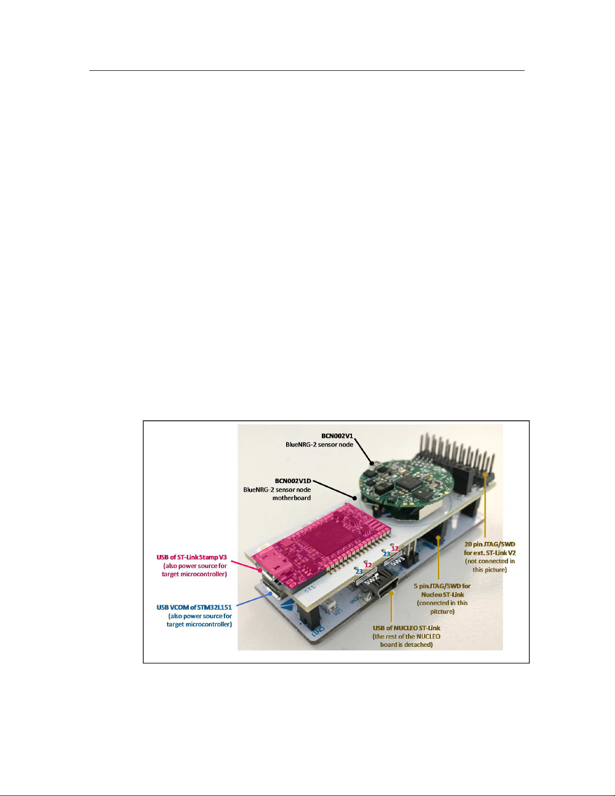
Figure 6. BlueNRG-2 sensor node (BCN002V1) on the top is connected to its
motherboard (BCN002V1D) in the middle, which in turn is connected to a NUCLEO ST-
Link on the bottom.
Page 23

UMXXX
9. How to program and debug
In order to Flash and debug the BlueNRG-2 sensor node BCN002V1, the corresponding
motherboard BCN002V1D is needed.
The following software must be installed on the computer:
• STSW-STM32102 STM32 Virtual COM port driver (VCOM), not needed for
Windows 10.
• STSW-BNRGFLASHER utility to Flash using any of the options illustrated below
(options A, B, C or D).
• STSW-BNRG1STLINK utility to Flash and debug using an ST-Link (see below,
options B, C or D).
The user MUST remove the battery from the BlueNRG-2 sensor node, then plug the
sensor node on its motherboard as shown in figure 6.
Four different options are supported to Flash and debug:
A. Flash using the motherboard (BCN002V1D), no debug is possible.
1. SW2 and SW3 switches must be in position 2-3 to connect the
BlueNRG-2 to the STM32L151 microcontroller on the motherboard.
2. Plug the USB of the motherboard to the computer to power the target
microcontroller and connect the UART VCOM
3. Run the STSW-BNRGFLASHER utility. The utility will exploit the
microcontroller which is assembled on the motherboard (STM32L151)
B. Flash and debug using the motherboard (BCN002V1D) and the NUCLEO ST-Link
V2 (connected and shown in figure 6).
1. Plug the 5-pin JTAG/SWD connector of motherboard to the corresponding
connector of the NUCLEO ST-Link
2. Plug the USB of the motherboard to power the target microcontroller
3. Plug the USB of the NUCLEO ST-Link to the computer to connect the
UART VCOM
4. Run the STSW-BNRG1STLINK utility. The utility will exploit the
microcontroller of the NUCLEO ST-Link.
C. Flash and debug using the motherboard (BCN002V1) and an external ST-Link V2
(not connected and not shown in figure 6).
1. Plug the 20-pin JTAG/SWD connector to the external ST-Link
Page 24

UMXXX
2. Plug the USB of the motherboard to power the target microcontroller
3. Plug the USB of the external ST-Link to the computer to connect the UART
VCOM
4. Run the STSW-BNRG1STLINK utility. The utility will exploit the
microcontroller of the external ST-Link.
D. Flash and debug using the motherboard (BCN002V1) with ST-Link Stamp V3
assembled (assembled and shown in figure 6).
1. The ST-Link Stamp V3 must be soldered on the motherboard
2. SW2 and SW3 switches must be in position 1-2 to connect the
BlueNRG-2 to the microcontroller on the ST-Link Stamp V3.
3. Plug the USB of the ST-Link V3 to the computer to power the target
microcontroller and connect the UART VCOM
4. Run the STSW-BNRG1STLINK utility. The utility will exploit the
microcontroller of the ST-Link Stamp V3.
10. Application firmware
Here are few hints for application developers: TBD
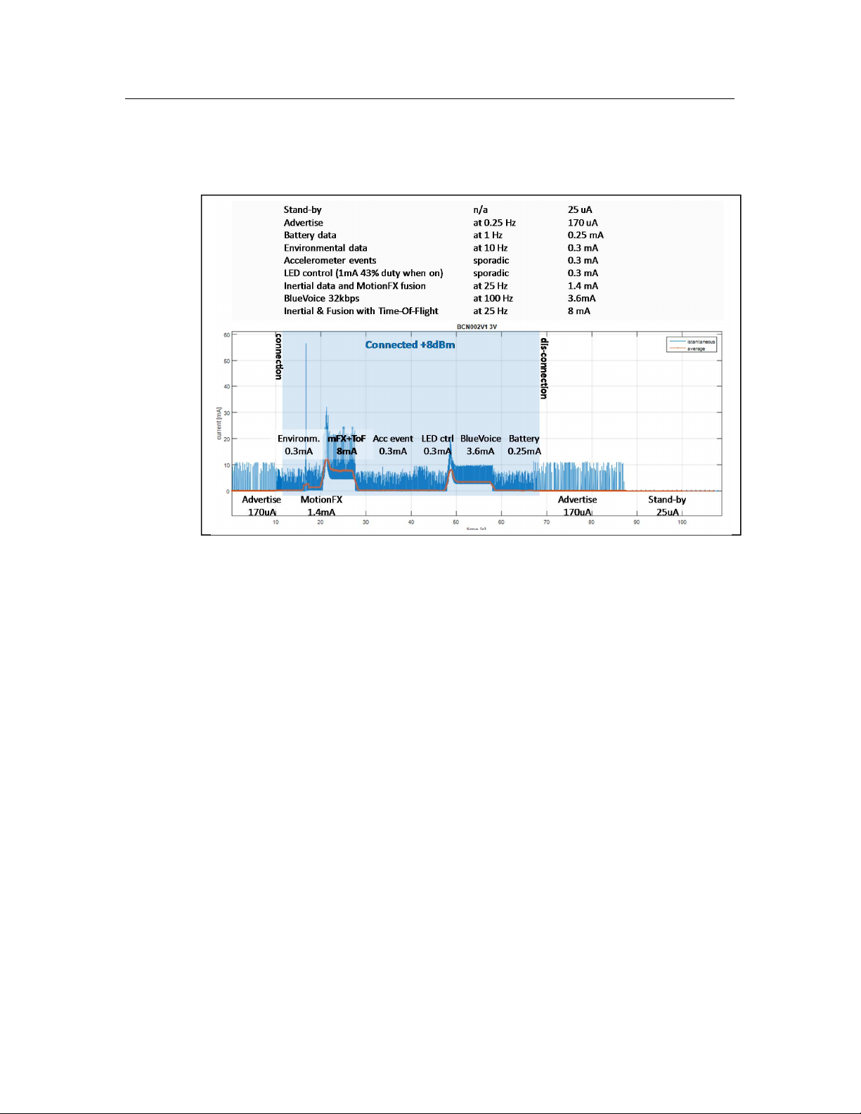
Table 3. Reference power consumption.
Active phase Inactive phase
(power not gated by MCU)
LED 150 uA (On) 0 uA (Off)
LSM6DSO Acc+Gyro 3 uA (LP, 50Hz) 0.05 uA (power-down)
HTS221 Rel. Humidity 22.5 uA (max avg, 1Hz) 0.5 uA (power-down)
LPS22HH Barometer 4 uA (LP, one-shot) 1 uA (power-down)
Figure 9. Example firmware application
Page 25
UMXXX
11. System performance
TBD.
Figure 10. Average current consumption for the example application
12. Schematic
Include schematic already formatted (see companion document).
13. Bill of Materials
Include BOM table already formatted (see companion document).
14. References
• AN5192 LSM6DSO always-on 3D accelerometer and 3D gyroscope
• AN5069 LIS2MDL ultra-low-power high-performance 3D magnetometer
• TN0018 surface mounting guidelines for MEMS sensors in LGA package
(LSM6DSO, LIS2MDL)
• AN5209 LPS22HH MEMS nano pressure sensor
• AN4722 HTS221 digital humidity sensor: hardware guidelines for system
integration
• TN1219 HTS221 digital humidity sensor reference design implementation
Page 26

UMXXX
• TN1218 Interpreting humidity and temperature readings in the HTS221 digital
humidity sensor
• TN1198 surface mount guidelines for MEMS sensors in HLGA packages
(LPS22HH, HTS221, MP34DT05-A)
• AN4428 best practices in the manufacturing process of MEMS microphones
• AN4427 gasket design for optimal acoustic performance in MEMS microphones
• AN4426 tutorial for MEMS microphones
• AN5191 using the programmable region of interest (ROI) with the VL53L1X
• UM2356 VL53L1X API user manual
Figure 12. VL53L1X is a Class 1 laser product
15. Safety Information
All usages not specified by the manufacturer may compromise the protection insured by the
device.
• VL53L1X contains a laser emitter; the device is designed to limit the laser
output within Class 1 laser safety limits under all conditions including single
faults, in compliance with IEC 60825-1:2014 (third edition). Recommended
settings and operating conditions specified in VL53L1X datasheet and user
manual MUST be respected. The laser output MUST NOT be increased by any
means and no optics should be to used focus the laser beam. Use of controls
or adjustments or performance of procedures other than those specified in
VL53L1X datasheet and user manual may result in hazardous radiation
Page 27

UMXXX
exposure.
• VL53L1X has an operating range from -20 to +85 degrees. Other components on
BlueNRG-2 sensor node have an operating temperature range from -40 to +85
Celsius degrees. The BlueNRG-2 low-energy wireless system-on-chip has a larger
operating range from -40 to +105 Celsius degrees. The ambient temperature and
relative humidity sensor HTS221 has the largest operating range up to +120
Celsius degrees.
• Operating ambient pressure goes from 260 to 1260 hPa. The LSM6DSO
accelerometer sensor may be sensitive to extreme changes in ambient pressure.
Others?
• Operating ambient relative humidity goes from 0 to 100% rH. Please note that the
BlueNRG-2 sensor node board is NOT PROTECTED against condensation of
water. A suitable water-resistant coating must be applied to the board and its
components. Note that any difference in the thermal expansion coefficient will
create mechanical stress between the PCB and the plastic package of the
components. This may affect MEMS sensors (LSM6DSO accelerometer and
gyroscope, LIS2MDL magnetometer, LPS22HH ambient pressure sensor, HTS221
ambient temperature and relative humidity sensor, MP34DT05-A microphone and
VL53L1 time-of-flight sensor). When coating is applied, the venting hole in the
package of LPS22HH and HTS221 should be covered not to contaminate the
sensing element. VL53L1X operates at 940nm wavelength (infrared) and coating,
if present, must be transparent to this wavelength; VL53L1X is strongly advised to
compensate for the optical effects of the coating.
• Please note that, the main component limiting the temperature, humidity and
ambient pressure operating range is the battery. Depending on the chemistry,
typical batteries have very limited or no functionality at or below 0 Celsius degrees.
Moreover, rechargeable batteries cannot operate above +45 Celsius degrees. A
suitable energy source must be selected for operation at low/high temperatures,
ambient pressure or relative humidity.
Operating Conditions for each component
• BlueNRG-2 low-energy wireless system-on-chip in QFN32 package: -40 to +105
Celsius degrees.
• LSM6DSO accelerometer and gyroscope: -40 to +85 Celsius degrees. Max shock
20000 g for 0.2s.
• LIS2MDL magnetometer: -40 to +85 Celsius degrees. Magnetic dynamic range +/-
Page 28

UMXXX
50 Gauss when magnetic field is aligned with any axis, +/-25 Gauss when it is not
aligned. Automatic recovery is activated when larger fields are removed. Recovery
is complete if larger field does not exceed 1200 Gauss; if 1200 Gauss limit is
exceeded, there will be a residual magnetization of +/-100mGauss for X and Y, +/500mGauss for Z axis. The residual magnetization, if any, can be estimated and
compensated as it is done for hard-iron effects (see corresponding paragraph). Max
field 10000 Gauss.
• LPS22HH ambient pressure sensor in HLGA-10L package: -40 to +85 Celsius
degrees; 260 to 1260 hPa ambient pressure. Max pressure 2MPa.
• HTS221 relative humidity and temperature sensor in HLGA-6L package: -40 to
+120 Celsius degrees; 0 to 100% rH ambient relative humidity. Max temperature
+125 Celsius degrees.
• MP34DT05-A digital microphone: -40 to +85 Celsius degrees.
• VL53L1X time-of-flight ranging sensor: -20 to +85 Celsius degrees; moisture
sensitivity level 3 (MSL) as described in IPC/JEDEC JSTD-020-C.
• CR2032 typical Lithium/Manganese-Dioxide battery has 220mAh nominal capacity
and 3V open-circuit voltage at room temperature. At -20 Celsius, open-circuit
voltage is reduced from 3V down to 2.2-2.7V for 1k-100kohm loads; capacity is
reduced from 220mAh down to 45-175mAh for 1k-100kohm loads. The inability of
the battery to sustain peak currents at low temperatures may prevent correct
system operation.
16. Limitations and disclaimers
For convenience, here is a summary of the limitations in the operating conditions of the
BlueNRG-2 sensor node:
• LSM6DSO, LIS2MDL, LPS22HH and HTS221 MEMS sensors
o Mechanical stress on the package (e.g. caused by PCB bending) may
affect the measurement accuracy of all sensors.
o Conducted heat may affect measurement accuracy, especially for the
environmental sensor HTS221: see AN4722 for details.
• Operating conditions for normal operation
o Temperature between -20 and +85 Celsius degrees; but care must be
taken to ensure battery performance below 0 degrees, and above 45
degrees.
Page 29

UMXXX
o Ambient pressure between 260 and 1260 hPa; please note that extreme
values or fast variations may cause mechanical stress in the sensor
package and affect measurement accuracy.
o Relative humidity between 0 and 100%; please note that use of the heating
element in HTS221 may be required to restore sensor operation in case of
condensation; please note that the board is not protected against
condensation of water.
o FCC part 15 Subpart C verification conditions: indoor environment,
temperature up to 45degC, Humidity range between 20% and 80%.
17. Compliance Information
FCC Compliance Statement
Part 15.19
This device complies with Part 15 of the FCC Rules. Operation is subject to the following
two conditions: (1) this device may not cause harmful interference, and (2) this device must
accept any interference received, including interference that may cause undesired
operation.
Part 15.105
This equipment has been tested and found to comply with the limits for a Class A digital
device, pursuant to part 15 of the FCC Rules. These limits are designed to provide
reasonable protection against harmful interference when the equipment is operated in a
commercial environment. This equipment generates, uses, and can radiate radio frequency
energy and, if not installed and used in accordance with the instruction manual, may cause
harmful interference to radio communications. Operation of this equipment in a residential
area is likely to cause harmful interference in which case the user will be required to correct
the interference at his own expense.
Part 15.21
Any changes or modifications to this equipment not expressly approved by
STMicroelectronics may cause harmful interference and void the user’s authority to operate
this equipment.
IC Compliance Statement
Compliance Statement
This device contains licence-exempt transmitter(s)/receiver(s) that comply with
Innovation, Science and Economic Development Canada’s licence-exempt RSS(s).
Operation is subject to the following two conditions:
Page 30

UMXXX
1. This device may not cause interference
2.
This device must accept any interference, including interference that may
cause undesired
operation of the device
Déclaration de conformité
Cet appareil contient un ou plusieurs émetteurs / récepteurs exemptés de licence
conformes à la norme Innovation, Science (s) RSS exemptés de licence par Science et
Développement économique Canada.
L’exploitation est autorisée aux deux conditions suivantes:
(1) l’appareil ne doit pas produire de brouillage
(2) l’utilisateur de l’appareil doit accepter tout brouillage radioélectrique subi, même si le
brouillage est susceptible d’en compromettre le fonctionnement.
EU RED
STEVAL-BCN002V1B bundle kit complies with the following European EMI/EMC and safety directives and
standards:
•
EN 300 328 V 2.1.1 (2016-11) (a)
•
ETSI EN 301 489-17 V3.1.1 (2017-02) (b)
•
ETSI EN 301 489-1 V2.1.1 (2017-02) (c)
•
EN 60950-1:2006 + A11:2009 + A1:2010 + A12:2011 + A2:2013 (d)
•
EN 62311:2008
The module is provided by CE marking:
Figure 9. CE marking
The module has obtained the RED certificate: No.
(certification in progress)
The certified module production firmware release is: 1.X
For additional information please refer to:
STMicroelectronics Via C. Olivetti, 2 Agrate Brianza 20864 (ITALY)
Page 31

UMXXX
Standard
Bluetooth Low Energy
Antenna
Embedded
RF Frequency
2402
-
2480
MHz
Max Output Power
8 dBm
Simplified EU Declaration of Conformity
Hereby, STMicroelectronics SRL declares that the radio equipment type STEVALBCN002V1B is in compliance with Directive 2014/53/EU.
The full text of the EU declaration of conformity is available at the following internet address:
www.st.com/bluetile
18.
Radio Features
Table 1: Radio features
19.
Antenna specifications
The STEVAL-BC002V1B comes with embedded ceramic antenna.
The table below represents the antenna specifications.
Antenna specifications
Nr. Of authorized antenna types 1
Antenna type Dedicated on PCB
Maximum total gain +1.6 dBi max
External Power amplifier Not present
Table 2: Antenna features
The table below represents the evaluation of exemption limit.
Table 3: Evaluation of Exemption Limit
Page 32

UMXXX
2402
8
+1,6 9,12 15,15
2440
8
+1,6 9,12 14,94
2480
8
+1,6 9,12 15,15
Given the values shown in tables above, the minimum usage distance is set to: 15 mm.
Évaluation de l'exemption limite:
Déclaré par le fabricant
Évaluation de l'exemption limite (distance de séparation 15mm)
Limite
d'exemption
(Obtenu par
interpolation
linéaire) (mW)
Fréquence
maximale
Puissance rayonnée
maximale
Max gain
d'antenne
maximum
dBm mW
Niveau
Table 4: Évaluation de l'exemption limite
Étant donné les valeurs indiquées dans les tableaux ci-dessus, la distance d'utilisation minimale
est définie sur: 15 mm.
20. Revision History
Table 8. Document revision history
Page 33

UMXXX
Date Revision Changes
13-Aug-2018 1 A.Vitali: Document draft, some chapter completed.
12-Nov-2018 2 A.Cucchi: Updated chapters for to the radio certifications
21. Contents
1. Introduction ................................................................................................... 1
2. Features........................................................................................................ 2
3. System architecture ...................................................................................... 4
4. BlueNRG-2 features ...................................................................................... 6
5. Inertial MEMS sensors features .................................................................... 9
6. Environmental MEMS sensors features ...................................................... 15
7. Digital MEMS microphone features ............................................................. 18
8. Time-of-Flight sensor features .................................................................... 20
9.
How to program and debug
........................................................................... 23
10.
11.
12.
13.
14.
Application firmware
System performance
Schematic
Bill of Materials
References
.................................................................................................... 25
.................................................................................................. 25
..................................................................................... 24
..................................................................................... 25
............................................................................................. 25
15. Safety Information ....................................................................................... 26
16.
17.
18.
19.
20.
Limitations and disclaimers
Compliance Information
Radio Features
............................................................................................. 31
Antenna specifications
Revision History
........................................................................................... 32
........................................................................... 28
................................................................................ 29
.................................................................................. 31
21. Contents ..................................................................................................... 33
Page 34

UMXXX
STMicroelectronics NV and its subsidiaries (“ST”) reserve the right to make changes, corrections, enhancements, modifications, and
improvements to ST products and/or to this document at any time without notice. Purchasers should obtain the latest relevant information on
ST products before placing orders. ST products are sold pursuant to ST’s terms and conditions of sale in place at the time of order
acknowledgement.
Purchasers are solely responsible for the choice, selection, and use of ST products and ST assumes no liability for application assistance or
the design of Purchasers’ products.
No license, express or implied, to any intellectual property right is granted by ST herein.
Resale of ST products with provisions different from the information set forth herein shall void any warranty granted by ST for such product.
ST and the ST logo are trademarks of ST. All other product or service names are the property of their respective owners.
Information in this document supersedes and replaces information previously supplied in any prior versions of this document.
IMPORTANT NOTICE – PLEASE READ CAREFULLY
© 2015 STMicroelectronics – All rights reserved
April 2017 DocIDXXXXX Rev 2 1/35
www.st.com
Page 35

UMXXX
 Loading...