

Page 1
STD4NK50ZD - STD4NK50ZD-1
1
3
3
3
1
3
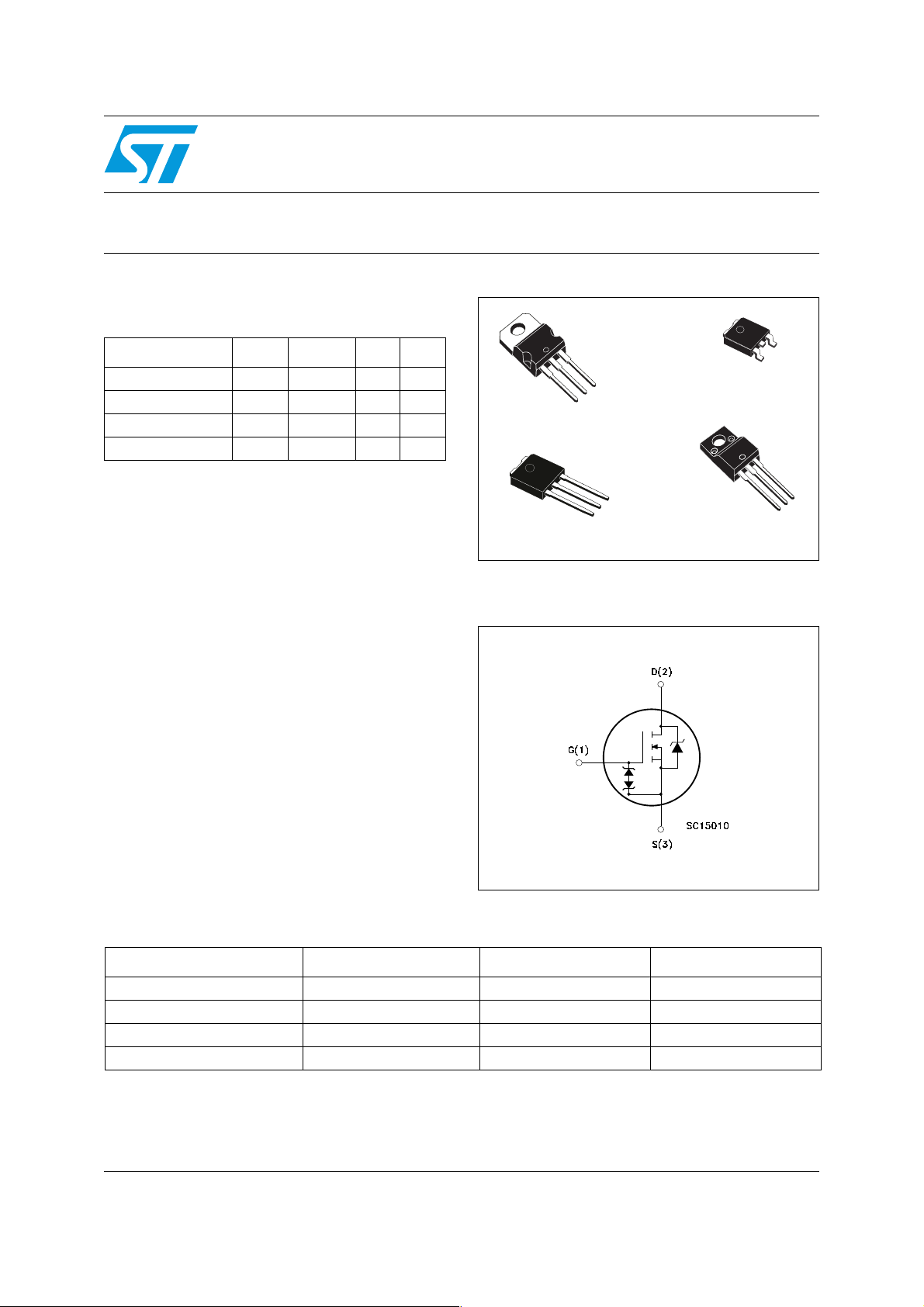
STF4NK50 ZD - STP4NK50ZD
N-channel 500V - 2.4Ω - 3A - TO-220 - TO-220FP- DPAK - IPAK
Fast diode SuperMESH™ Power MOSFET
General features
Type V
STD4NK50ZD-1 500V <2.7Ω 3A 45W
STD4NK50ZD 500V <2.7Ω 3A 45W
STF4NK50ZD 500V <2.7Ω 3A 20W
STP4NK50ZD 500V <2.7Ω 3A 45W
■ 100% avalanche tested
■ Extremely high dv/dt capability
■ Gate charge minimized
■ Very low intrinsic capacitances
■ Very good manufacturing repeability
DSS
R
DS(on)ID
Pw
TO-220
IPAK
2
2
1
DPAK
TO-220FP
1
2
Description
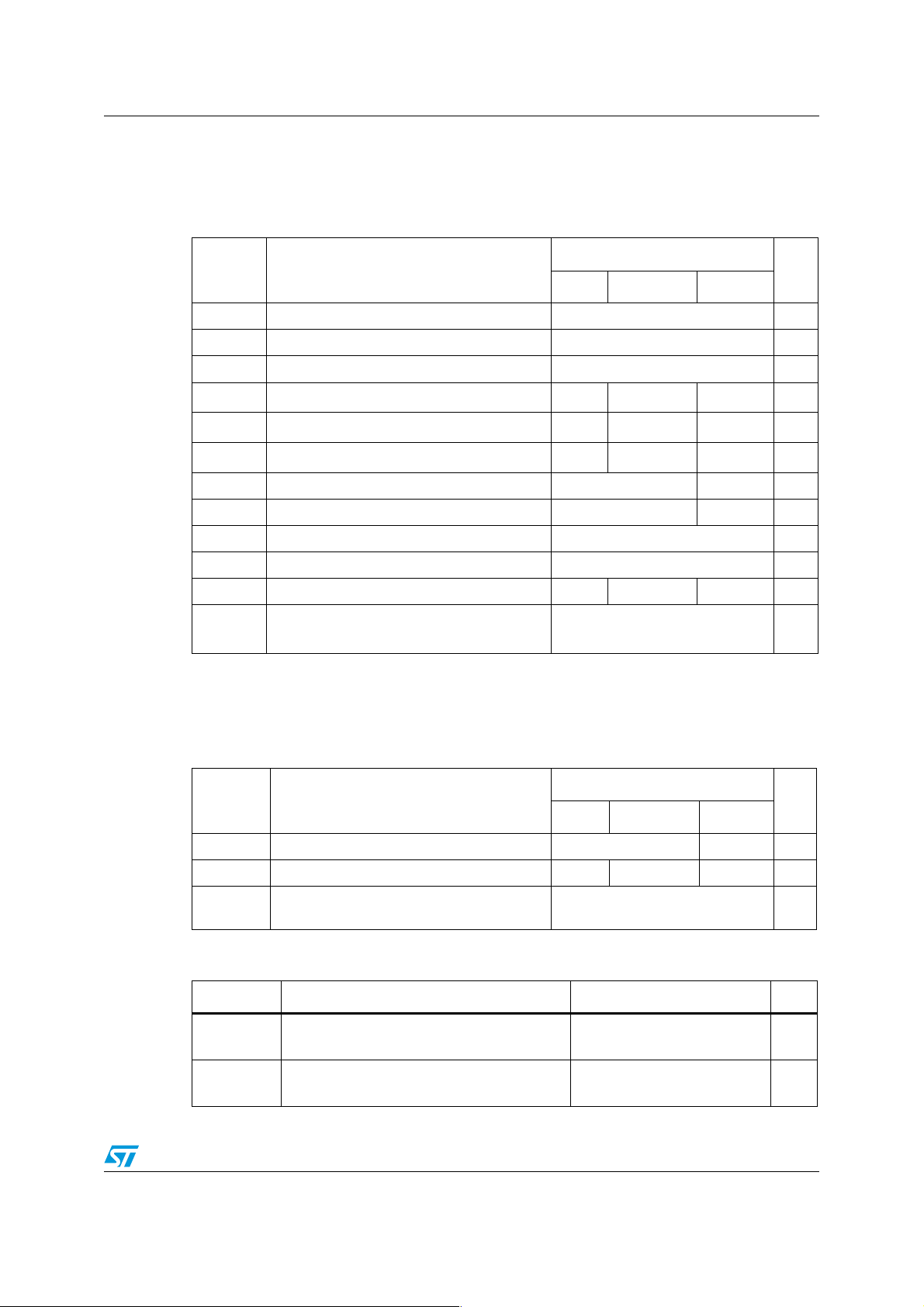
The fast SuperMESH™ series as sociate s all
advantages of reduced on-resistance, zener gate
protection and outstanding dc/dt capability with a
Fast body-drain recovery diode. Such series
complements the FDmesh™ advanced tecnology.
Applications
■ Switching application
Order codes
Part number Marking Package Packaging
STD4NK50ZD-1 D4NK50ZD-1 IPAK Tube
STD4NK50ZD D4NK50ZD DPAK Tape & reel
STF4NK50ZD F4NK50ZD TO-220FP Tube
STP4NK50ZD P4NK50ZD TO-220 Tube
Internal schematic diagram
April 2006 Rev 3 1/17
www.st.com
17
Page 2

Contents STD4NK50ZD - STD4NK50ZD-1 - STF4NK50ZD - STP4NK50ZD
Contents
1 Electrical ratings . . . . . . . . . . . . . . . . . . . . . . . . . . . . . . . . . . . . . . . . . . . . 3
2 Electrical characteristics . . . . . . . . . . . . . . . . . . . . . . . . . . . . . . . . . . . . . 5
2.1 Electrical characteristics (curves) . . . . . . . . . . . . . . . . . . . . . . . . . . . . 6
3 Test circuit . . . . . . . . . . . . . . . . . . . . . . . . . . . . . . . . . . . . . . . . . . . . . . . 10
4 Package mechanical data . . . . . . . . . . . . . . . . . . . . . . . . . . . . . . . . . . . . 11
5 Packaging mechanical data . . . . . . . . . . . . . . . . . . . . . . . . . . . . . . . . . . 16
6 Revision history . . . . . . . . . . . . . . . . . . . . . . . . . . . . . . . . . . . . . . . . . . . 17
2/17
Page 3
STD4NK50ZD - STD4NK50ZD-1 - STF4NK50ZD - STP4NK50ZD Electrical ratings
1 Electrical ratings
Table 1. Abs olute maxim um ratings
Value
Symbol Parameter
TO-220 IPAK/DPAK TO-220FP
Unit
V
I
P
V
DGR
V
I
I
DM
TOT
Drain-source voltage (VGS = 0) 500 V
DS
Drain-gate voltage (RGS = 20KΩ) 500 V
Gate-source voltage ± 30 V
GS
Drain current (continuous) at TC = 25°C 3
D
Drain current (continuous) at TC=100°C 1.9
D
(2)
Drain current (pulsed) 12
Total dissipation at TC = 25°C 45 20 W
Derating factor 0.36 0.16 W/°C
V
ESD(G-D)
dv/dt
V
T
T
1. Limited only by max im um temper a tu r e all ow e d
2. Pulse width limited by safe operating area
3. ISD ≤3A, di/dt ≤200A/µs, VDD =80%V
Gate source ESD(HBM-C=100pF, R=1.5KΩ) 2800 V
(3)
Peak diode recovery voltage slope 15 V/ns
Insulation withstand voltage (DC) -- -- 2500 V
ISO
Operating junction temperature
J
Storage temperature
stg
(BR)DSS
Table 2. Th erm al resi stance
3
1.9
12
(1)
(1)
(1)
3
1.9
12
(1)
(1)
(1)
-55 to 150 °C
A
A
A
Value
Symbol Parameter
TO-220 IPAK/DPAK TO-220FP
R
thj-case
R
thj-a
T
Thermal resistance junction-case Max 2.78 6.25 °C/W
Thermal resistance junction-ambient Max 62.5 100 62.5 °C/W
Maximum lead tempera ture for soldering
l
purpose
300 °C
Table 3. Avalanche data
Symbol Parameter Value Unit
I
AR
E
AS
Avalanche current, repetitive or not-repetiti ve
(pulse width limited by Tj Max)
Single pulse avalanche energy
(starting Tj=25°C, Id=Iar, Vdd=50V)
3A
120 mJ
Unit
3/17
Page 4
Electrical characteristics STD4NK50ZD - STD4NK50ZD-1 - STF4NK50ZD - STP4NK50ZD
2 Electrical characteristics
(T
=25°C unless otherwise specified)
CASE
Table 4. On /off states
Symbol Parameter T est condictions Min. T yp. Max. Unit
V
(BR)DSS
I
DSS
I
GSS
V
GS(th)
R
DS(on)
Drain-source breakdown
voltage
Zero gate voltage drain
current (V
GS
= 0)
Gate body leakage curren t
= 0)
(V
DS
Gate threshold voltage
Sta ti c drain-source on
resistance
I
= 1mA, VGS= 0
D
V
= Max rating,
DS
= Max rating @125°C
V
DS
= ±20V
V
GS
V
= VGS, ID = 50µA
DS
V
= 10V, ID= 1.5A
GS
500 V
1
50
±10 µA
2.5 3.5 4.5 V
2.3 2.7 Ω
Table 5. Dyn amic
Symbol Parameter Test condictions Min. Typ. Max. Unit
C
oss eq
(1)
g
fs
C
C
C
Forward transconductance
Input capacitance
iss
Output capacitance
oss
Reverse transfe r
rss
capacitance
(2)
Equivalent output
.
capacitance
=15V, ID = 1.5A
V
DS
= 25V, f = 1 MHz,
V
DS
V
= 0
GS
V
= 0, V
GS
DS
=0V to 400V
1.5 S
310
49
10
33 pF
µA
µA
pF
pF
pF
Q
g
Total gate charge
Q
Q
1. Pulsed: pulse duration=300 µs, duty cycle 1.5%
2. C
inceases from 0 to 80% V
Gate-source charge
gs
Gate-drain char ge
gd
is def ined as a constant eq uivalent capacitance gi ving the same charging time as C
oss eq.
DSS
V
V
(see Figure 11)
Table 6. Swi tching times
Symbol Pa rameter Test condictions Min. T yp. Max. Unit
t
d(on)
t
d(off)
4/17
Turn-on delay time
t
Rise time
r
Turn-off del ay tim e
Fall time
t
f
V
R
(see Figure 18)
= 400V, ID = 3A
DD
=10V
GS
= 250 V, ID= 1.5A,
DD
= 4.7Ω, V
G
GS
=10V
12
3
7
9.5
15.5
23
22
when VDS
oss
nC
nC
nC
ns
ns
ns
ns
Page 5
STD4NK50ZD - STD4NK50ZD-1 - STF4NK50ZD - STP4NK50ZD Electrical characteristics
Table 7. S ource drain diode
Symbol Parameter Test condictions Min Typ. Max Unit
I
SD
I
SDM
V
SD
t
Q
I
RRM
t
Q
I
RRM
1. Pulse width limited by safe operating area
2. Pulsed: pulse duration=300 µs, duty cycle 1.5%
Source -drain current 3 A
(1)
Source-drain current (pulsed) 12 A
(2)
Forward on voltage
rr
Reverse rec overy time
Reverse recovery charge
rr
Reverse rec overy current
rr
Reverse rec overy time
Reverse Recovery Char ge
rr
Reverse rec overy current
= 3A, VGS=0
I
SD
= 3A,
I
SD
di/dt = 100A/µs,
= 34V, Tj = 25°C
V
DD
= 3A,
I
SD
di/dt = 100A/µs,
= 34V, Tj = 150°C
V
DD
73
140
3.82
118
260
4.4
1.6 V
Table 8. Gate-source zen er di ode
Symbol Parameter Test condictions Min. Typ. Max Unit
Gate-source braekdown
(1)
BV
GSO
1. The bui lt-in b ack-to-back Zener diodes have specifically been designed to enhance not onl y the device’s
ESD capability, but also to make them safely absorb possible voltage transients that may occasionally be
applied from gate to source. In this respect the Zener voltage is appropriate to achieve an efficient and
cost-effective intervention to protect the device’s integrity. These integrated Zener diodes thus avoid the
usage of ex te r na l co mp on ents.
voltage
= ±1mA (open drain) 30 V
I
GS
ns
nC
A
ns
nC
A
5/17
Page 6
Electrical characteristics STD4NK50ZD - STD4NK50ZD-1 - STF4NK50ZD - STP4NK50ZD
2.1 Electrical characteristics (curves)
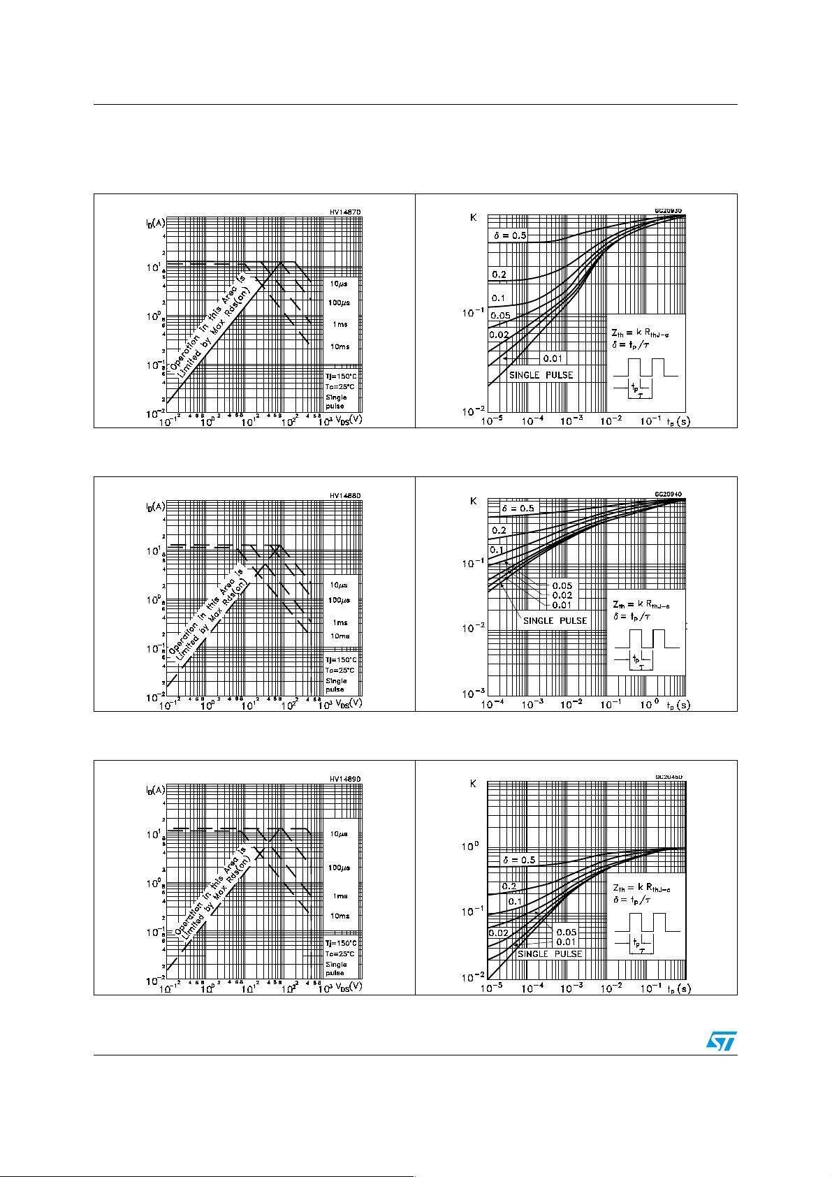
Figure 1. Safe operating area for TO-220 Figure 2. Thermal impedance for TO-220
Figure 3. Safe operating areafor TO-220FP Figure 4. Thermal impedance for TO-220FP
Figure 5. Safe operating area for DPAK/IPAK Figure 6. Thermal impedance for DPAK/IPAK
6/17
Page 7

STD4NK50ZD - STD4NK50ZD-1 - STF4NK50ZD - STP4NK50ZD Electrical characteristics
Figure 7. Output characterisics Figure 8. Transfer characteristics
Figure 9. Transconductance Figure 10. Static drain-source on resistance
Figure 11. Gate charge vs gate-source voltage Figure 12. Capacitance variations
7/17
Page 8

Electrical characteristics STD4NK50ZD - STD4NK50ZD-1 - STF4NK50ZD - STP4NK50ZD
Figure 13. Normalized gate threshold voltage
vs temperature
Figure 15. Source-drain diode forward
characteristics
Figure 14. Normalized on resistance vs
temperature
Figure 16. Normalized B
vs temperature
VDSS
Figure 17. Maxim um aval anch e ener gy vs
temperature
8/17
Page 9

STD4NK50ZD - STD4NK50ZD-1 - STF4NK50ZD - STP4NK50ZD Test circuit
3 Test circuit
Figure 18. Switching times test circuit for
resistive load
Figure 20. Test circuit for inductive load
switching and diode recovery times
Figure 19. Gate charge test circuit
Figure 21. Unclamped inductive load test
circuit
Figure 22. Unclamped inductive waveform Figure 23. Switching time waveform
9/17
Page 10

Package mechanical data STD4NK50ZD - STD4NK50ZD-1 - STF4NK50ZD - STP4NK50ZD
4 Package mechanical data
In order to meet environmental requirements, ST offers these devices in ECOPA CK ®
packages. These packages have a Lead-free second level interconnect . The category of
second level interconnect is marked on the package and on the inner box label, in
compliance with JEDEC Standard JESD97. The maximum ratings related to soldering
conditions are also marked on the inner box label. ECOPACK is an ST trademark.
ECOPACK specifications are available at: www.st.com
10/17
Page 11

STD4NK50ZD - STD4NK50ZD-1 - STF4NK50ZD - STP4NK50ZD Packag e m echa nical data
TO-220 MECHANICAL DATA
DIM.
A 4.40 4.60 0.173 0.181
b 0.61 0.88 0.024 0.034
b1 1.15 1.70 0.045 0.066
c 0.49 0.70 0.019 0.027
D 15.25 15.75 0.60 0.620
E 10 10.40 0.393 0.409
e 2.40 2.70 0.094 0.106
e1 4.95 5.15 0.194 0.202
F 1.23 1.32 0.048 0.052
H1 6.20 6.60 0.244 0.256
J1 2.40 2.72 0.094 0.107
L 13 14 0.511 0.551
L1 3.50 3.93 0.137 0.154
L20 16.40 0.645
L30 28.90 1.137
øP 3.75 3.85 0.147 0.151
Q 2.65 2.95 0.104 0.116
MIN. TYP MAX. MIN. TYP. M AX.
mm. inch
11/17
Page 12

Package mechanical data STD4NK50ZD - STD4NK50ZD-1 - STF4NK50ZD - STP4NK50ZD
0068771-E
TO-251 (IPAK) MECHANICAL DATA
DIM.
MIN. TYP. MAX. MIN. TYP. MAX.
mm inch
A 2.2 2.4 0.086 0.094
A1 0.9 1.1 0.035 0.043
A3 0.7 1.3 0.027 0.051
B 0.64 0.9 0.025 0.031
B2 5.2 5.4 0.204 0.212
B3 0.85 0.033
B5 0.3 0.012
B6 0.95 0.037
C 0.45 0.6 0.017 0.023
C2 0.48 0.6 0.019 0.023
D 6 6.2 0.236 0.244
E 6.4 6.6 0.252 0.260
G 4.4 4.6 0.173 0.181
H 15.9 16.3 0.626 0.641
L 9 9.4 0.354 0.370
L1 0.8 1.2 0.031 0.047
L2 0.8 1 0.031 0.039
H
C
A
C2
D
E
= =
L2
B2
= =
12/17
A1
L
B3
B6
B
2
1 3
L1
B5
A3
G
= =
Page 13

STD4NK50ZD - STD4NK50ZD-1 - STF4NK50ZD - STP4NK50ZD Packag e m echa nical data
TO-252 (DPAK) MECHANICAL DATA
DIM.
A 2.20 2.40 0.087 0.094
A1 0.90 1.10 0.035 0.043
A2 0.03 0.23 0.001 0.009
B 0.64 0.90 0.025 0.035
B2 5.20 5.40 0.204 0.213
C 0.45 0.60 0.018 0.024
C2 0.48 0.60 0.019 0.024
D 6.00 6.20 0.236 0.244
E 6.40 6.60 0.252 0.260
G 4.40 4.60 0.173 0.181
H 9.35 10.10 0.368 0.398
L2 0.8 0.031
L4 0.60 1.00 0.024 0.039
V2 0
MIN. TYP. MAX. MIN. TYP. MAX.
o
mm inch
o
8
o
0
o
0
P032P_B
13/17
Page 14

Package mechanical data STD4NK50ZD - STD4NK50ZD-1 - STF4NK50ZD - STP4NK50ZD
TO-220FP MECHANICAL DATA
DIM.
A 4.4 4.6 0.173 0.181
B 2.5 2.7 0.098 0.106
D 2.5 2.75 0.098 0.108
E 0.45 0.7 0.017 0.027
F 0.75 1 0.030 0.039
F1 1.15 1.7 0.045 0.067
F2 1.15 1.7 0.045 0.067
G 4.95 5.2 0.195 0.204
G1 2.4 2.7 0.094 0.106
H 10 10.4 0.393 0.409
L2 16 0.630
L3 28.6 30.6 1.126 1.204
L4 9.8 10.6 .0385 0.417
L5 2.9 3.6 0.114 0.141
L6 15.9 16.4 0.626 0.645
L7 9 9.3 0.354 0.366
Ø 3 3.2 0.118 0.126
MIN. TYP MAX. MIN. TYP. MAX.
mm. inch
E
A
D
B
L3
L6
L7
F1
F
H
14/17
L2
L5
F2
G1
G
123
L4
Page 15

STD4NK50ZD - STD4NK50ZD-1 - STF4NK50ZD - STP4NK50ZD Pa ckag ing mecha nical data
5 Packaging mechanical data
DPAK FOOTPRINT
All dimensions are in millimeters
TAPE AND REEL SHIPMENT
REEL MECHANICAL DATA
DIM.
A 330 12.992
B 1.5 0.059
C 12.8 13.2 0.504 0.520
D 20.2 0.795
G 16.4 18.4 0.645 0.724
N 50 1.968
T 22.4 0.881
mm inch
MIN. MAX . MIN. MAX.
TAPE MECHANICAL DATA
DIM.
A0 6.8 7 0.267 0.275
B0 10.4 10.6 0.409 0.417
B1 12.1 0.476
D 1.5 1.6 0.059 0.063
D1 1.5 0.059
E 1.65 1.85 0.065 0.073
F 7.4 7.6 0.291 0.299
K0 2.55 2.75 0.100 0.108
P0 3.9 4.1 0. 153 0.161
P1 7.9 8.1 0.311 0.319
P2 1.9 2.1 0. 075 0.082
R 40 1.574
W 15.7 16.3 0.618 0.641
mm inch
MIN. MAX. MIN. MAX.
BASE QTY BULK QTY
2500 2500
15/17
Page 16

Revision history STD4NK50ZD - STD4NK50ZD-1 - STF4NK50ZD - STP4NK50ZD
6 Revision history
Table 9. Revision history
Date Revision Changes
09-Feb-2006 1 First Release
20-Feb-2006 2 Corrected Part Nu mber
27-Apr-2006 3 Modified curves on page 6
16/17
Page 17

STD4NK50ZD - STD4NK50ZD-1 - STF4NK50ZD - STP4NK50ZD
I
e
r
y
t
A
P
o
l
N
is
d
ts
o
h
t
U
D
W
D
W
S
O
U
D,
A
S,
N
R
S
R
id
a
y
l
Please Read Carefu ll y:
nformation in this document is provided solely in connection with ST products. STMicroelectronics NV and its subsidiaries (“ST”) reserve th
ight to make changes, corrections, modifications or improvements, to this document, and the products and services described herein at an
ime, without notice.
ll ST product s are sold pursuant to ST’s te rm s and condit io ns of sale.
urchasers are solely responsible for the choice, selection and use o f the ST products and services described herein, and ST assum es n
iability whatsoever relating to the choice, selection or use of the ST products and services described herein.
o license, express or implied, by estoppel or otherwise, to any intellectual property rights is granted under this document. If any part of th
ocument refers to any third party products or s ervices it s hall not be deem ed a licen se grant by ST for the use of such third party produc
r services , or any intel lec tual pro per ty cont aine d ther ein or con sidere d as a warra nty c overi ng th e use i n any mann er w hats oever of suc
hird part y products or s ervices or any i ntellectual property cont ai ned therein.
NLESS OTHERWISE SET FORTH IN ST’S TERMS AND CONDITIONS OF SALE ST DISCLAIMS ANY EXPRESS OR IMPLIE
ARRANTY WITH RESPECT TO THE USE AND/OR SALE OF ST PRODUCTS INCLUDING WITHOUT LIMITATION IMPLIE
ARRANTIES OF MERCHANTABILITY, FITNESS FOR A PARTICULAR PURPOSE (AND THEIR EQUIVALENTS UNDER THE LAW
F ANY JURISDICTION), OR INFRINGEMENT OF ANY PATENT, COPYRIGHT OR OTHER INTELLECTUAL PROPERTY RIGHT.
NLESS EXPRESSLY APPROVED IN WRI TING BY A N AUTH ORIZE REP RESENTATI VE OF S T, ST PRODUCTS ARE NOT DESIGNE
UTHORIZ ED OR WAR RANTED F OR USE IN MI L IT ARY, AI R CRAFT, SPACE, L IF E SAVING , OR LIFE SUSTAINING APPLICATIO N
OR IN PRODUCTS OR SYSTEMS, WHERE FAILURE OR MALFUNCTION MAY RESULT IN PERSONAL INJURY, DEATH, O
EVERE PROPERTY OR ENVIRONMENTAL DAMAGE.
esale of ST products with provisions different from the statements and/or technical features set forth in this document shall immediately vo
ny warran ty gr anted by ST fo r the ST produc t or se rvice d es cribed he rein and shall not c reat e o r extend in a ny mann er wha tsoe ve r, an
iability of ST.
The ST logo is a registered trademark of STMicroelectronics. All other names are the property of their respective owners.
ST and the ST logo are trademarks or registered tradem arks of ST in vari ous countries.
Information in this document super sedes and repla ces all inform ation previously supplied.
© 2006 STMi croelectro ni cs - All rights reserved
Austra l i a - Be l gi um - Brazil - C anada - China - Czech Republic - Finland - France - Germ any - Hong Kong - India - Israe l - It aly - Japan -
STMicroelectronic s group of companies
Malaysi a - M al ta - Morocco - Singapore - Spain - Swede n - Sw i tzerland - United Kingdom - United States of Ameri ca
www.st.com
17/17
 Loading...