

Page 1
STD22NM20N
3
N-CHANNEL 200V - 0.088Ω - 22A DPAK
ULTRA LOW GATE CHARGE MDmesh™ II MOSFET
Table 1: General Fe a ture s
TYPE V
STD22NM20N 200 V < 0.105 Ω 22 A
■ WORLDWIDE LOWEST GATE CHARGE
■ TYPICAL R
■ HIGH dv/dt and AVALANCHE CAPAB IL IT IES
■ LOW INPUT CAPACITANCE
■ LOW GATE RESISTAN CE
DS
DSS
(on) = 0.088 Ω
R
DS(on)
I
D
DESCRIPTION
This 200V MOS FET with a new advanced layout
brings all unique advantages of MDm esh technol
ogy to lower vol tages. The device exhi bits worldwide lowest gate charge for any given onresistance. Its use is therefore ideal as primary
switch in isolated DC-DC converters for Telecom
and Computer appli cations. Used in combination
with secondary-side low-voltage STripFET™
products, it contributes to reducting losses and
boosting effeciency.
APPLICATIONS
The MDmesh™ family is very suitable for increasing power density allowing system miniaturization
and higher efficiencies
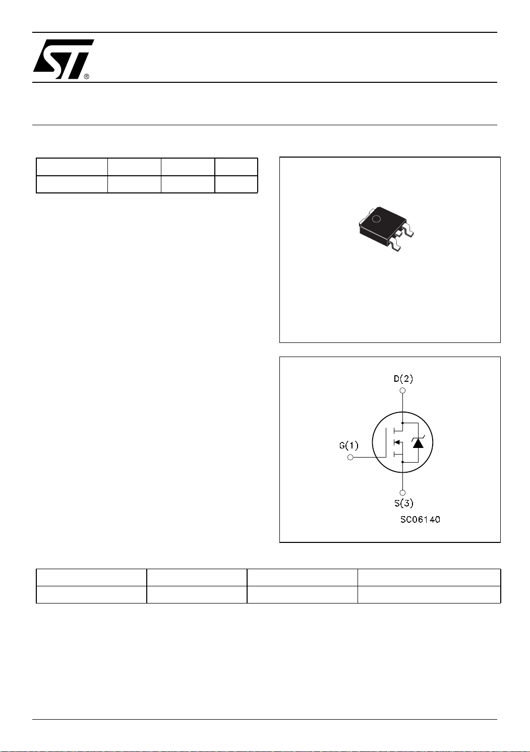
Figure 1: Package
1
DPAK
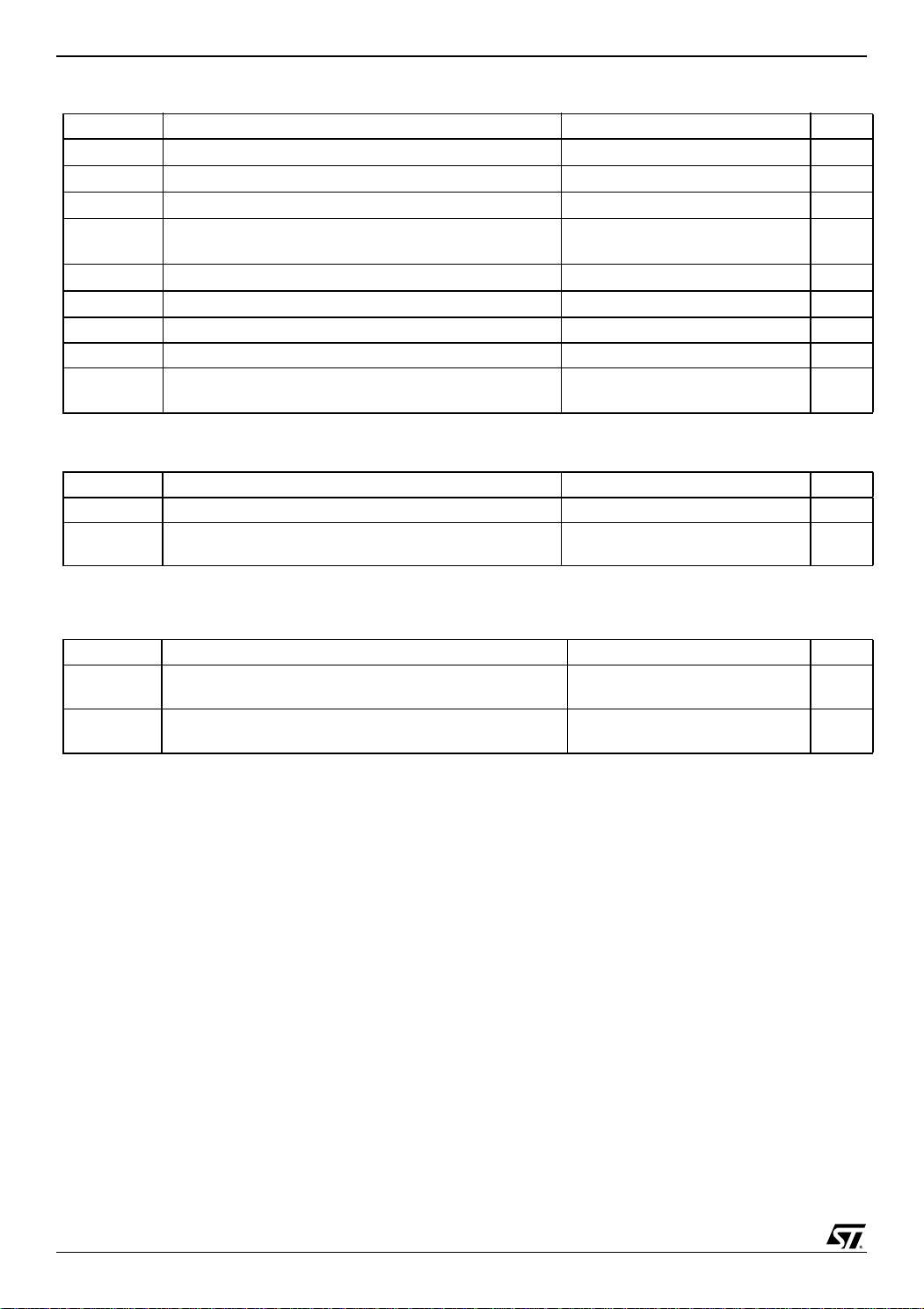
Figure 2: Internal Schematic Diagram
Table 2: Order Codes
SALES TYPE MARKING PACKAGE PACKAGING
STD22NM20NT4 D22NM20N DPAK TAPE & REEL
Rev. 5
1/10November 2005
Page 2
STD22NM20N
Table 3: Absolute Maximum ratings
Symbol Parameter Value Unit
V
DS
V
DGR
V
GS
I
D
I
DM
P
TOT
dv/dt (2) Peak Diode Recovery voltage slope 14 V/ns
T
j
T
stg
(*) ISD ≤ 22A, di/dt ≤ 400A/µs, VDD = 80% V
Table 4: Thermal Data
Rthj-case Thermal Resistance Junction-case Max 1.25 °C/W
Rthj-amb Thermal Resistance Junction-ambient Max 100 °C/W
Rthj-ambTlThermal Resistance Junction-pcb (*)
(*) When mounted on 1 inch² FR-4 board, 2 oz Cu, t ≤ 10 sec
Drain-source Voltage (VGS = 0) 200 V
Drain-gate Voltage (RGS = 20 kΩ) 200 V
Gate- source Voltage
Drain Current (continuous) at TC = 25°
Drain Current (continuous) at T
(*)
Drain Current (pulsed)
C =
100°
± 20 V
22
13.7
88 A
Total Dissipation at TC = 25°C 100 W
Derating Factor 0.8 W/°C
Storage Temperature
Max Operating Junction Temperature
(BR)DSS
150
-65 to 150
43
Maximum Lead Temperature For Soldering Purpose
275
A
A
°C
°C
°C/W
°C
Table 5: Avalanche Characteristics
Symbol Parameter Max Value Unit
I
AS
E
AS
Avalanche Current, Repetitive or Not-Repetitive
(pulse width limited by Tj max)
Single Pulse Avalanche Energy
(starting Tj = 25 °C, ID = 22 A, VDD = 50 V)
22 A
380 mJ
2/10
Page 3
STD22NM20N
ELECTRICAL CHARACTERISTICS (T
=25°C UNLESS OTHERWISE SPECIFIED)
CASE
Table 6: On/Off
Symbol Parameter Test Conditions Min. Typ. Max. Unit
V
(BR)DSS
Drain-source
ID = 1mA, VGS = 0 200 V
Breakdown Voltage
I
DSS
I
GSS
Zero Gate Voltage
Drain Current (VGS = 0)
Gate-body Leaka ge
VDS = Max Rating
VDS = Max Rating, TC = 125 °C
1
10
VGS = ± 20V 100 nA
Current (VDS = 0)
V
GS(th)
R
DS(on)
Gate Threshold Voltage
Static Drain-source On
VDS = VGS, ID = 250 µA 3.5 4.2 5 V
VGS = 10V, ID = 11 A 0.088 0.105 Ω
Resistance
Table 7: Dynamic
Symbol Parameter Test Conditions Min. Typ. Max. Unit
g
C
(**) C
(2)
fs
C
iss
C
oss
C
rss
oss eq. (**)
Forward Transconductance
Input Capacitance
Output Capacitance
Reverse Transfer
Capacitance
Equivalent Outpu t
Capacitiance
R
t
d(on)
t
t
r(Voff)
t
Q
Q
Q
oss eq.
G
r
f
g
gs
gd
Gate Input Resistance f= 1MHz Gate DC Bias = 0
Turn-on Delay Time
Rise Time
Turn-off Delay Time
Fall Time
Total Gate Charge
Gate-Source Charge
Gate-Drain Charge
is defi n ed as a constant equivalent capacitance gi vi ng the sam e charging tim e as C
VDS = 15 V, ID=11 A 8 S
VDS = 25V, f = 1 MHz, VGS = 0 800
330
130
VGS = 0 V, VDS = 0 V to 400 V 225 pF
5 Ω
Test Sgnal Level = 20 mV
Open Drain
VDD = 100 V, ID = 11 A
RG = 4.7Ω VGS = 10 V
(see Figure 15)
40
15
40
11
VDD = 100 V, ID = 20 A,
VGS = 10 V
(see Figure 19)
when VDS increases from 0 to 80% V
oss
32
25
50 nC
6
µA
µA
pF
pF
pF
ns
ns
ns
ns
nC
nC
DSS
Table 8: Source Drain Diode
Symbol Parameter Test Conditions Min. Typ. Max. Unit
I
SD
I
(1)
SDM
VSD (2)
t
rr
Q
rr
I
RRM
t
rr
Q
rr
I
RRM
(1) Pulse width limite d by safe operating area.
(2) Pulsed: Pulse durat i on = 300 µs, duty cycle 1.5 %
Source-drain Current
Source-drain Current (pulsed)
Forward On Voltage
Reverse Recovery Time
Reverse Recovery Charge
Reverse Recovery Current
Reverse Recovery Time
Reverse Recovery Charge
Reverse Recovery Current
ISD = 20 A, VGS = 0 1.3 V
ISD = 20 A, di/dt = 100 A/µs
VDD = 100V, Tj = 25°C
(see test circuit, Figure 17)
ISD = 20 A, di/dt = 100 A/µs
VDD = 100V, Tj = 150°C
(see test circuit, Figure 17)
160
960
12.8
225
1642
15
22
88
A
A
ns
µC
A
ns
µC
A
3/10
Page 4

STD22NM20N
Figure 3: Safe Operating Area
Figure 4: Output Characteristics
Figure 6: Thermal Impedance
Figure 7: Transfer Characteristics
Figure 5: Transconductance
4/10
Figure 8: Static Drain-source On Resistance
Page 5

STD22NM20N
Figure 9: Gate Charge vs Gate-source Voltag e
Figure 10: Normalized Gate Thereshold Voltage vs Temperature
Figure 12: Capacitance Variations
Figure 13: Normal ized On R esistance vs Temperature
Figure 11: S ource-Drain Diode Forward Characteristics
Figure 14: Normalized BVdss vs Temperature
5/10
Page 6

STD22NM20N
Figure 15: Unclamped Inductive Load Test Circuit
Figure 16: Switching Times Test Circuit For Resistive Load
Figure 18: Unclamped Inductive Wafeform
Figure 19: Gate Charge Test Circuit
Figure 17: Test Circuit For Inductive Load Switching and Diode Recovery Times
6/10
Page 7

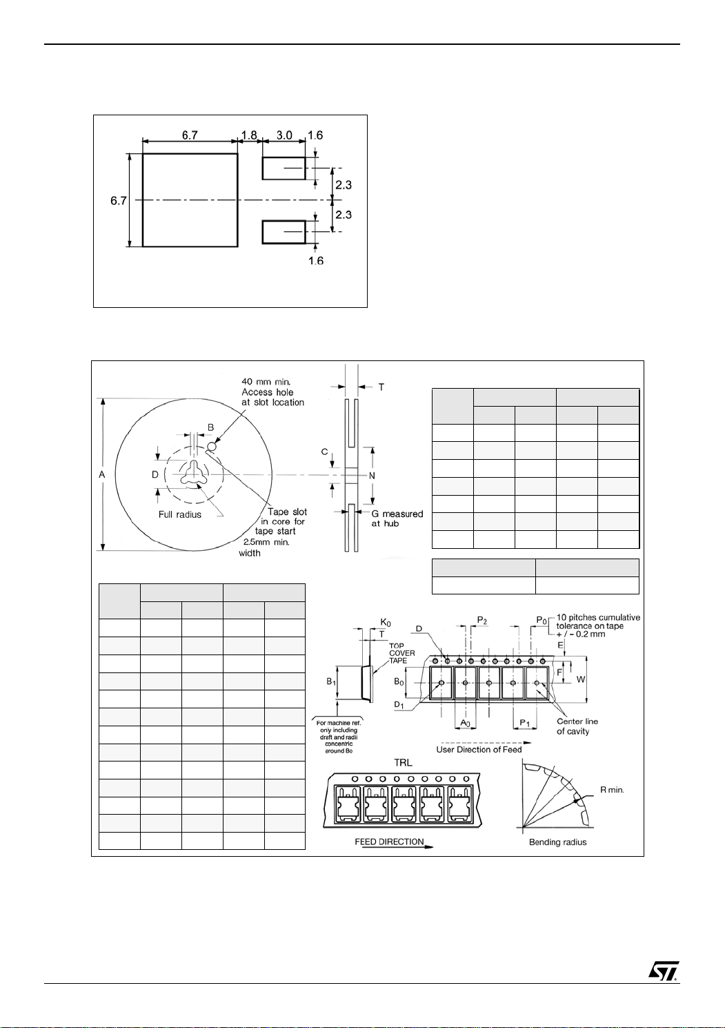
TO-252 (DPAK ) MECHANICAL DATA
STD22NM20N
DIM.
A 2.20 2.40 0.087 0.094
A1 0.90 1.10 0.035 0.043
A2 0.03 0.23 0.001 0.009
B 0.64 0.90 0.025 0.035
B2 5.20 5.40 0.204 0.213
C 0.45 0.60 0.018 0.024
C2 0.48 0.60 0.019 0.024
D 6.00 6.20 0.236 0.244
E 6.40 6.60 0.252 0.260
G 4.40 4.60 0.173 0.181
H 9.35 10.10 0.368 0.398
L2 0.8 0.031
L4 0.60 1.00 0.024 0.039
V2 0
MIN. TYP. MAX. MIN. TYP. MAX.
o
mm inch
o
8
o
0
o
0
P032P_B
7/10
Page 8
STD22NM20N
All dimensions are in millimeters
DPAK FOOTPRINT
TAPE AND REEL SHIPMENT
REEL MECHANICAL DATA
DIM.
A 330 12.992
B 1.5 0.059
C 12.8 13.2 0.504 0.520
D 20.2 0.795
G 16.4 18.4 0.645 0.724
N 50 1.968
T 22.4 0.881
mm inch
MIN. MAX. MIN. MAX.
TAPE MECHANICAL DATA
DIM.
A0 6.8 7 0.267 0.275
B0 10.4 10.6 0.409 0.417
B1 12.1 0.476
D 1.5 1.6 0.059 0.063
D1 1.5 0.059
E 1.65 1.85 0.065 0.073
F 7. 4 7.6 0.291 0.299
K0 2.55 2.75 0.100 0.108
P0 3.9 4.1 0.153 0.161
P1 7.9 8.1 0.311 0.319
P2 1.9 2.1 0.075 0.082
R 40 1.574
W 15.7 16.3 0.618 0.641
mm inch
MIN. MAX. MIN. MAX.
BASE QTY BULK QTY
2500 2500
8/10
Page 9

Table 9: Revision History
Date Revision Description of Change s
31-May-2004 1 First Release.
15-Mar-2005 2 Update version.
09-May-2005 3 Complete version.
09-Jun-2005 4 New update
04-Nov-2005 5 Corrected value on Table 8
STD22NM20N
9/10
Page 10

STD22NM20N
I
s
o
d
b
t
t
t
a
nformation furnished is believed to be accurate and reliable. However, STMicroelectronics assumes no responsibility for the consequence
f use of such information nor for any infringement of patents or other rights of third parties which may result from its use. No license is grante
y implicat io n or ot h er wis e under an y pat e nt or pa te nt r igh ts of STMi c roe l ec tro ni c s. Sp ec i fi ca ti on s ment i o ne d in th is p ub li c ati on ar e s ub jec
o change without notice. This publication supersedes and repla ces all information previously supplied. STMicroel ectronics products are no
uthorized for use as critical components in life support devices or systems without express written approval of STMicroelectronics.
The ST logo is a registered trademark of STMicroelectronics
All other names are the property of their respective owners
Australia - Belgium - Brazil - Canada - China - Czech Republic - Finland - France - Germany - Hong Kong - India - Israel - Italy - Japan -
Malaysia - Malta - Morocco - Singapore - Spain - Sweden - Switzerland - United Kingdom - United States of America
© 2005 STMicroelectronics - All Rights Reserved
STMicroelectronics group of companies
10/10
 Loading...