

STMicroelectronics STD17NF03L, STD17NF03L-1 Technical data
N-channel 30V - 0.038Ω - 17A - DPAK/IPAK
3
General features
Type V
STD17NF03L-1 30V <0.05Ω 17A
STD17NF03L 30V <0.05Ω 17A
■ Exceptional dv/dt capability
■ Low gate charge at 100°C
■ Application oriented characterization
■ 100% avalanche tested
DSS
Description
This Power MOSFET is the latest development of
STMicroelectronis unique "Single Feature Size™"
strip-based process. The resulting transistor
shows extremely high packing density for low onresistance, rugged avalanche characteristics and
less critical alignment steps therefore a
remarkable manufacturing reproducibility.
R
DS(on)
I
D
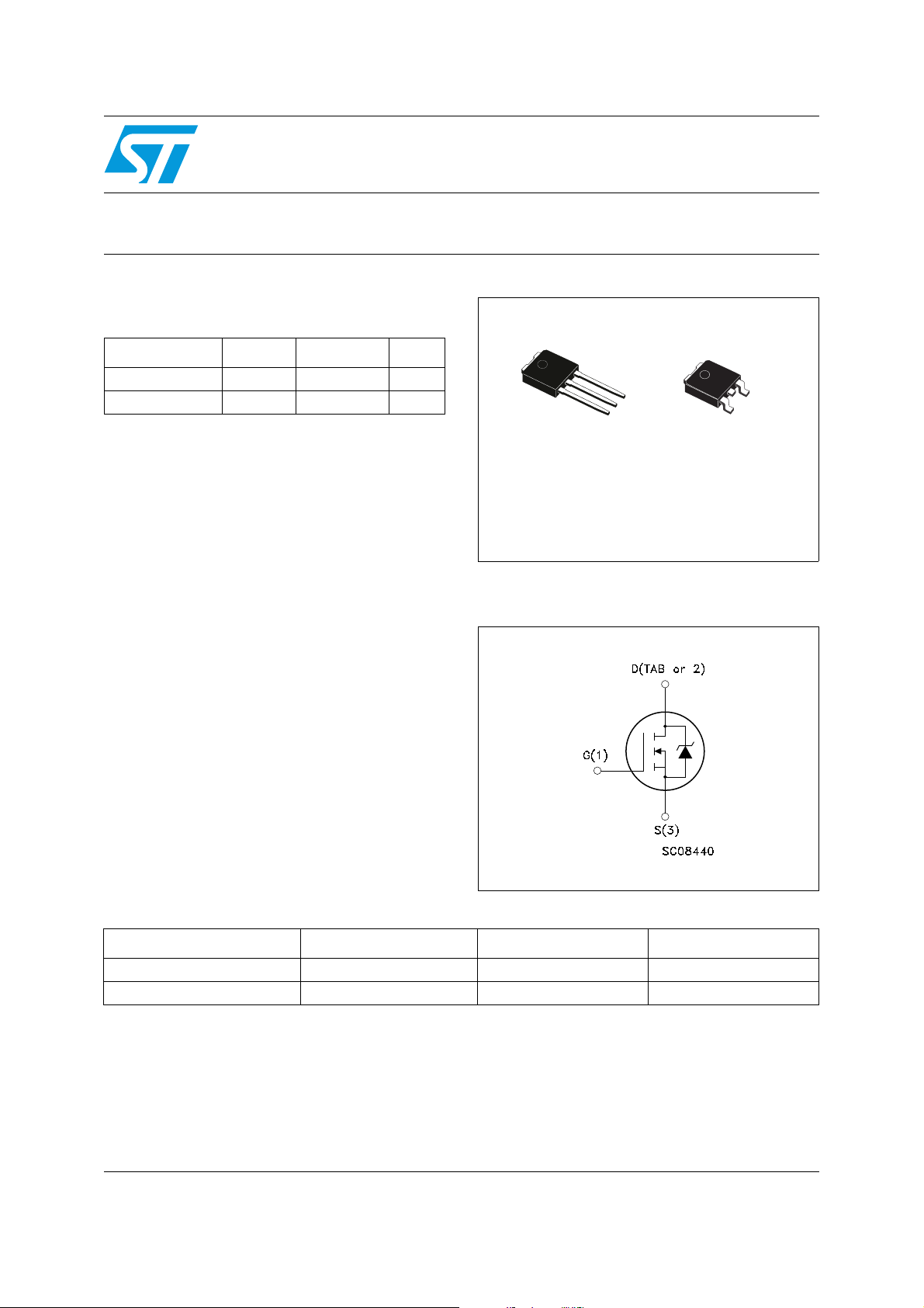
STD17NF03L
STD17NF03L-1
STripFET™ II Power MOSFET
2
1
iPAK
DPAK
Internal schematic diagram
3
1
Applications
■ Switching application
Order codes
Part number Marking Package Packaging
STD17NF03L-1 D17NF03L@ IPAK Tube
STD17NF03LT4 D17NF03L@ DPAK Tape & reel
July 2006 Rev 3 1/14
www.st.com
14

Contents STD17NF03L - STD17NF03L-1
Contents
1 Electrical ratings . . . . . . . . . . . . . . . . . . . . . . . . . . . . . . . . . . . . . . . . . . . . 3
2 Electrical characteristics . . . . . . . . . . . . . . . . . . . . . . . . . . . . . . . . . . . . . 4
2.1 Electrical characteristics (curves) . . . . . . . . . . . . . . . . . . . . . . . . . . . . . 6
3 Test circuit . . . . . . . . . . . . . . . . . . . . . . . . . . . . . . . . . . . . . . . . . . . . . . . . 8
4 Package mechanical data . . . . . . . . . . . . . . . . . . . . . . . . . . . . . . . . . . . . . 9
5 Packing mechanical data . . . . . . . . . . . . . . . . . . . . . . . . . . . . . . . . . . . . 12
6 Revision history . . . . . . . . . . . . . . . . . . . . . . . . . . . . . . . . . . . . . . . . . . . 13
2/14
STD17NF03L - STD17NF03L-1 Electrical ratings
1 Electrical ratings
Table 1. Absolute maximum ratings
Symbol Parameter Value Unit
V
I
V
DGR
V
DM
P
I
I
DS
GS
D
D
(1)
tot
Drain-source voltage (VGS = 0) 30 V
Drain-gate voltage (RGS = 20 kΩ)30V
Gate- source voltage ± 16 V
Drain current (continuous) at TC = 25°C 17 A
Drain current (continuous) at TC = 100°C 12 A
Drain current (pulsed) 68 A
Total dissipation at TC = 25°C 30 W
Derating Factor 0.2 W/°C
(2)
dv/dt
(3)
E
AS
T
stg
T
j
1. Pulse width limited by safe operating area.
2. ISD ≤17A, di/dt ≤ 300A/µs, VDD =V
3. Starting Tj = 25 °C, ID = 8.5A, VDD = 15V
Peak diode recovery avalanche energy 7 V/ns
Single pulse avalanche energy 200 mJ
Storage temperature
-55 to 175 °C
Max. operating junction temperature
, Tj ≤ T
(BR)DSS
JMAX
Table 2. Thermal data
Rthj-case Thermal resistance junction-case max 5.0 °C/W
Rthj-amb Thermal resistance junction-to ambient max 100 °C/W
T
J
Maximum lead temperature for soldering purpose 275 °C
3/14
Electrical characteristics STD17NF03L - STD17NF03L-1
2 Electrical characteristics
(T
=25°C unless otherwise specified)
CASE
Table 3. On/off states
Symbol Parameter Test conditions Min. Typ. Max. Unit
V
(BR)DSS
I
DSS
I
GSS
V
GS(th)
R
DS(on)
Drain-source
breakdown voltage
Zero gate voltage
drain current (V
GS
Gate-body leakage
current (V
DS
= 0)
= 0)
ID = 250µA, VGS =0 30 V
V
= Max rating
DS
VDS = Max rating,
= 125°C
T
C
1
10
VGS = ± 16V ±100 nA
Gate threshold voltage VDS = VGS, ID = 250µA 1 1.5 2.2 V
Static drain-source on
resistance
= 10V, ID = 8.5A
V
GS
= 5V, ID = 8.5A
V
GS
0.038
0.045
0.05
0.06
Table 4. Dynamic
Symbol Parameter Test conditions Min. Typ. Max. Unit
fs
C
C
C
transconductance
Input capacitance
iss
Output capacitance
oss
Reverse transfer
rss
capacitance
Forward
(1)
g
VDS > I
D(on)
R
DS(on)max, , ID
= 25V, f = 1MHz,
V
DS
VGS = 0
x
=8.5A
12 S
320
155
28
µA
µA
Ω
Ω
pF
pF
pF
t
d(on)
t
t
d(off)
t
Q
Q
Q
1. Pulsed: Pulse duration = 300 µs, duty cycle 1.5 %.
Turn-on delay time
Rise time
r
Turn-off delay time
Fall time
f
Total gate charge
g
Gate-source charge
gs
Gate-drain charge
gd
V
R
(see Figure 13)
VDD = 3024V, ID = 17A,
V
(see Figure 14)
4/14
= 15V, ID = 8.5A
DD
=4.7Ω VGS = 5V
G
= 5V, RG=4.7Ω
GS
11
100
25
22
4.8
2.25
1.7
ns
ns
ns
ns
6.5 nC
nC
nC

STD17NF03L - STD17NF03L-1 Electrical characteristics
Table 5. Source drain diode
Symbol Parameter Test conditions Min. Typ. Max. Unit
I
SD
I
SDM
V
SD
t
Q
I
RRM
1. Pulse width limited by safe operating area.
2. Pulsed: Pulse duration = 300 µs, duty cycle 1.5 %
Source-drain current
Source-drain current
(1)
(pulsed)
(2)
Forward on voltage ISD = 17A, VGS = 0 1.5 V
Reverse recovery time
rr
Reverse recovery charge
rr
Reverse recovery current
ISD = 17A, di/dt = 100A/µs,
VDD = 15V, Tj = 150°C
(see Figure 15)
28
18
1.3
22
88
A
A
ns
nC
A
5/14
 Loading...