

STMicroelectronics STA518 Service Manual
Feature
■ Multipower BCD technology
■ Minimum input output pulse width distortion
■ 200mΩ R
complementary dmos output
dsON
stage
■ CMOS compatible logic inputs
■ Thermal protection
■ Thermal warning output
■ Under voltage protection
■ Short circuit protection
Description
STA518 is a monolithic quad half bridge stage in
Multipower BCD Technology. The device can be
used also as dual bridge or reconfigured, by
connecting CONFIG pin to Vdd pin, as single
bridge with double current capability.
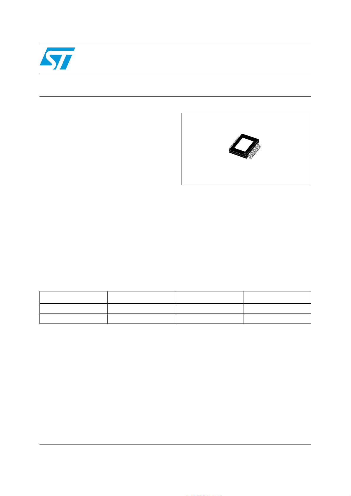
STA518
40V 3.5A quad power half bridge
PSSO36 (slug up)
The device is particularly designed to make the
output stage of a stereo All-Digital High Efficiency
(DDX™) amplifier capable to deliver an output
power of 24W x 4 channels @ THD = 10% at Vcc
30V on 4W load in single ended configuration.
It can also deliver 50 + 50W @ THD = 10% at Vcc
29V as output power on 8W load in BTL
configuration and 70W @ THD = 10% at Vcc 34V
on 8W in single paralleled BTL configuration.
The input pins have threshold proportional to VL
pin voltage
.
Order codes
Part number Temp range, °CPackage Packing
STA518 -40 to 90 PowerSSO36 (slug up) Tube
STA51813TR -40 to 90 PowerSSO36 (slug up) Tape & reel
May 2006 Rev 3 1/19
www.st.com
1

Contents STA518
Contents
1 Audio application circuit . . . . . . . . . . . . . . . . . . . . . . . . . . . . . . . . . . . . . . 5
2 Pins description . . . . . . . . . . . . . . . . . . . . . . . . . . . . . . . . . . . . . . . . . . . . 6
3 Electrical specifications . . . . . . . . . . . . . . . . . . . . . . . . . . . . . . . . . . . . . . 8
3.1 Absolute maximum ratings . . . . . . . . . . . . . . . . . . . . . . . . . . . . . . . . . . . . . 8
3.2 Recommended operating conditions . . . . . . . . . . . . . . . . . . . . . . . . . . . . . 8
3.3 Thermal data . . . . . . . . . . . . . . . . . . . . . . . . . . . . . . . . . . . . . . . . . . . . . . . 8
3.4 Thermal information . . . . . . . . . . . . . . . . . . . . . . . . . . . . . . . . . . . . . . . . . . 8
3.5 Electrical characteristcs . . . . . . . . . . . . . . . . . . . . . . . . . . . . . . . . . . . . . . . 9
4 Technical information . . . . . . . . . . . . . . . . . . . . . . . . . . . . . . . . . . . . . . . 12
4.1 Logic interface and decode: . . . . . . . . . . . . . . . . . . . . . . . . . . . . . . . . . . . 12
4.2 Power outputs: . . . . . . . . . . . . . . . . . . . . . . . . . . . . . . . . . . . . . . . . . . . . . 13
4.3 Parallel output / high current operation: . . . . . . . . . . . . . . . . . . . . . . . . . . 13
4.4 Additional informations: . . . . . . . . . . . . . . . . . . . . . . . . . . . . . . . . . . . . . . 13
5 Characterization curves . . . . . . . . . . . . . . . . . . . . . . . . . . . . . . . . . . . . . 15
6 Package information . . . . . . . . . . . . . . . . . . . . . . . . . . . . . . . . . . . . . . . . 17
7 Revision history . . . . . . . . . . . . . . . . . . . . . . . . . . . . . . . . . . . . . . . . . . . 18
2/19

STA518 List of tables
List of tables
Table 1. Pin Function . . . . . . . . . . . . . . . . . . . . . . . . . . . . . . . . . . . . . . . . . . . . . . . . . . . . . . . . . . . . . 6
Table 2. Functional Pin Status . . . . . . . . . . . . . . . . . . . . . . . . . . . . . . . . . . . . . . . . . . . . . . . . . . . . . . 7
Table 3. Absolute maximum ratings . . . . . . . . . . . . . . . . . . . . . . . . . . . . . . . . . . . . . . . . . . . . . . . . . . 8
Table 4. Recommended operating conditions . . . . . . . . . . . . . . . . . . . . . . . . . . . . . . . . . . . . . . . . . . 8
Table 5. Thermal data . . . . . . . . . . . . . . . . . . . . . . . . . . . . . . . . . . . . . . . . . . . . . . . . . . . . . . . . . . . . 8
Table 6. Electrical Characteristcs . . . . . . . . . . . . . . . . . . . . . . . . . . . . . . . . . . . . . . . . . . . . . . . . . . . 9
Table 7. VLOW, VHIGH variation with I
Table 8. Logic Truth Table (see Figure 4) . . . . . . . . . . . . . . . . . . . . . . . . . . . . . . . . . . . . . . . . . . . . 10
Table 9. Document revision history . . . . . . . . . . . . . . . . . . . . . . . . . . . . . . . . . . . . . . . . . . . . . . . . . 18
bias . . . . . . . . . . . . . . . . . . . . . . . . . . . . . . . . . . . . . . . . . . . . . . . . . . . . . . . 10
3/19

List of figures STA518
List of figures
Figure 1. Audio application circuit ( Quad single ended) . . . . . . . . . . . . . . . . . . . . . . . . . . . . . . . . . . . 5
Figure 2. Pin Connection (top view) . . . . . . . . . . . . . . . . . . . . . . . . . . . . . . . . . . . . . . . . . . . . . . . . . . . 6
Figure 3. Low current dead time for Single End application: test circuit. . . . . . . . . . . . . . . . . . . . . . . 11
Figure 4. High current dead time for Bridge application: block diagram . . . . . . . . . . . . . . . . . . . . . . 11
Figure 5. High current dead time for Bridge application: test circuit. . . . . . . . . . . . . . . . . . . . . . . . . . 11
Figure 6. STA518 Block Diagram Full-Bridge DDX® or Binary Modes . . . . . . . . . . . . . . . . . . . . . . . 12
Figure 7. STA518 Block Diagram Binary Half-Bridge Mode . . . . . . . . . . . . . . . . . . . . . . . . . . . . . . . 12
Figure 8. Typical Stereo Full Bridge Configuration . . . . . . . . . . . . . . . . . . . . . . . . . . . . . . . . . . . . . . 14
Figure 9. Typical Single BTL Configuration . . . . . . . . . . . . . . . . . . . . . . . . . . . . . . . . . . . . . . . . . . . . 14
Figure 10. Power Dissipation vs Output Power . . . . . . . . . . . . . . . . . . . . . . . . . . . . . . . . . . . . . . . . . . 15
Figure 11. Power Derating Curve . . . . . . . . . . . . . . . . . . . . . . . . . . . . . . . . . . . . . . . . . . . . . . . . . . . . 15
Figure 12. THD+N vs Output Power . . . . . . . . . . . . . . . . . . . . . . . . . . . . . . . . . . . . . . . . . . . . . . . . . . 15
Figure 13. Output Power vs Supply Voltage . . . . . . . . . . . . . . . . . . . . . . . . . . . . . . . . . . . . . . . . . . . . 15
Figure 14. THD vs Frequency . . . . . . . . . . . . . . . . . . . . . . . . . . . . . . . . . . . . . . . . . . . . . . . . . . . . . . . 15
Figure 15. Output Power vs Supply Voltage . . . . . . . . . . . . . . . . . . . . . . . . . . . . . . . . . . . . . . . . . . . . 16
Figure 16. THD+N vs Output Power . . . . . . . . . . . . . . . . . . . . . . . . . . . . . . . . . . . . . . . . . . . . . . . . . . 16
Figure 17. Power Dissipation vs Output Power . . . . . . . . . . . . . . . . . . . . . . . . . . . . . . . . . . . . . . . . . . 16
Figure 18. THD+N vs Output Power . . . . . . . . . . . . . . . . . . . . . . . . . . . . . . . . . . . . . . . . . . . . . . . . . . 16
Figure 19. PSSO36 (Slug Up) Mechanical Data & Package Dimensions . . . . . . . . . . . . . . . . . . . . . . 17
4/19
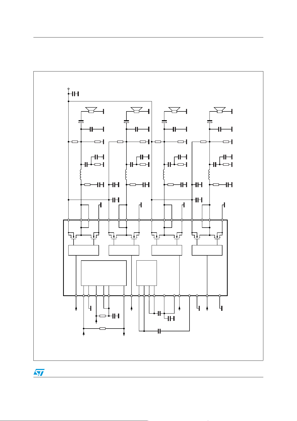
STA518 Audio application circuit
1 Audio application circuit
Figure 1. Audio application circuit ( Quad single ended)
CC
C21
2200µF
+V
4Ω
1µF
C91
C31 820µF
5K
R61
L11 22µH
1P
CC
V
OUTPL
17
15
C71
R41
16
100nF
20
OUTPL
5K
R62
C81
100nF
6
R51
C41
330pF
PGND1P
14
C61
C51
1N
CC
V
121011
R63
100nF
1µF
OUTNL
4Ω
1µF
C92
C32 820µF
5K
L12 22µH
C72
100nF
R42
OUTNL
R645KR65
C82
100nF
R52
20
C42
PGND1N
13
6
330pF
C33 820µF
2P
CC
V
7
4Ω
1µF
C93
5K
L13 22µH
OUTPR
8
C73
R43
9
100nF
20
OUTPR
5K
R66
C83
100nF
6
R53
C43
330pF
PGND2P
6
C62
C52
2N
CC
V
423
R67
100nF
1µF
OUTNR
4Ω
1µF
C94
C34 820µF
5K
L14 22µH
OUTNR
C74
R44
100nF
20
PGND2N
5
R68
C84
R54
5K
100nF
6
C44
330pF
D03AU1474
M3
292324
L
V
IN1A
IN1A
+3.3V
CONFIG
M2
&
PROTECTIONS
252726
FAULT
PWRDNPWRDN
10K
R59
10K
R57
LOGIC
M5
28
TH_WAR
TRI-STATE
C58
100nF
M4
3021223334
DDVDD
V
IN1B
IN1B
TH_WAR
M17
REGULATORS
SS
VSSV
C53
C58
SIGN
V
100nF
100nF
M15
35
36
31
IN2A
SIGN
CC
CC
V
IN2A
C60
100nF
20
GND-Reg
GND-Clean
M16
19
32
IN2B
IN2B
M14
1
GNDSUB
5/19
Pins description STA518
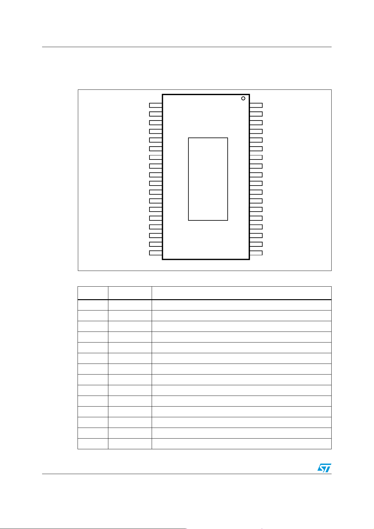
2 Pins description
Figure 2. Pin Connection (top view)
V
Sign
CC
VCCSign
V
SS
V
SS
IN2B
IN1B
IN1A
FAULT
TRI-STATE
PWRDN
CONFIG
V
L
V
DD
V
DD
Table 1. Pin Function
36
35
34
33
32
31
30
29
28
26
25
23
22
21
20
19
D01AU1273
1027
11
12
1324
14
15
16
17
18
1
2
3
4
5
6
7
8
9
GND-SUB
OUT2B
OUT2B
2B
V
CC
GND2B
GND2AIN2A
V
2A
CC
OUT2A
OUT2ATH_WAR
OUT1B
OUT1B
V
1B
CC
GND1B
GND1A
1A
V
CC
OUT1A
OUT1AGND-Reg
N.C.GND-Clean
N° Pin Description
1 GND-SUB Substrate ground
2 ; 3 OUT2B Output half bridge 2B
4 Vcc2B Positive supply
5 GND2B Negative Supply
6 GND2A Negative Supply
7 Vcc2A Positive supply
8 ; 9 OUT2A Output half bridge 2A
10 ; 11 OUT1B Output half bridge 1B
12 Vcc1B Positive supply
13 GND1B Negative Supply
14 GND1A Negative Supply
15 Vcc1A Positive supply
16 ; 17 OUT1A Output half bridge 1A
35 ; 36 Vcc Sign Signal Positive supply
6/19
 Loading...