

Page 1

ST7LITE1
8-BIT MCU WITH SINGLE VOLTAGE FLASH MEMORY,
DATA EEPROM, ADC, 4 TIMERS, SPI
■ Memories
– 4 Kbytes single voltage extended Flash
(XFlash) Program memory with read-out protection, In-Circuit Programming and In-Application programming (ICP and IAP). 10K write/
erase cycles guaranteed, data retention: 20
years at 55°C.
– 256 bytes RAM
2
– 128 bytes data E
PROM with read-out protection. 300K write/erase cycles guaranteed,
data retention: 20 years at 55°C.
■ Clock, Reset and Supply Management
– Enhanced reset system
– Enhanced low voltage supervisor (LVD) for
main supply and an auxiliary voltage detector
(AVD) with interrupt capability for implementing safe power-down procedures
– Clock sources: Internal 1% RC oscillator (on
some devices), crystal/ceramic resonator or
external clock
– Internal 32-MHz input clock for Auto-reload
timer
– Optional x4 or x8 PLL for 4 or 8 MHz internal
clock
– Five Power Saving Modes: Halt, Active-Halt,
Auto Wake-up from Halt, Wait and Slow
■ I/O Ports
– Up to 15 multifunctional bidirectional I/O lines
–7 high sink outputs
■ 4 Timers
– Configurable watchdog timer
– Two 8-bit Lite Timers with prescaler,
1 realtime base and 1 input capture
– One 12-bit Auto-reload Timer with 4 PWM
outputs, input capture and output compare
functions
■ Communication Interface
– SPI synchronous serial interface
■ Interrupt Management
– 10 interrupt vectors plus TRAP and RESET
– 15 external interrupt lines (on 4 vectors)
■ A/D Converter
– 7 input channels
– Fixed gain Op-amp
– 13-bit precision for 0 to 430 mV (@ 5V V
– 10-bit precision for 430 mV to 5V (@ 5V V
■ Instruction Set
– 8-bit data manipulation
– 63 basic instructions with illegal opcode de-
tection
– 17 main addressing modes
– 8 x 8 unsigned multiply instructions
■ Development Tools
– Full hardware/software development package
– DM (Debug Module)
Device Summary
Features ST7LITE10 ST7LITE15 ST7LITE19
Program memory - bytes 4K
RAM (stack) - bytes 256 (128)
Data EEPROM - bytes - - 128
Peripherals
Operating Supply 2.4V to 5.5V
CPU Frequency
Operating Temperature -40°C to +85°C
Packages SO20 300”
Lite Timer with Watchdog,
Autoreload Timer, SPI,
10-bit ADC with Op-Amp
Up to 8Mhz
(w/ ext OSC up to 16MHz)
Lite Timer with Watchdog,
Autoreload Timer with 32-MHz input clock,
SPI, 10-bit ADC with Op-Amp
Up to 8Mhz (w/ ext OSC up to 16MHz
and int 1MHz RC 1% PLLx8/4MHz)
SO20
DD
DD
)
)
Rev. 2.0
December 2004 1/131
1
Page 2

Table of Contents
1 INTRODUCTION . . . . . . . . . . . . . . . . . . . . . . . . . . . . . . . . . . . . . . . . . . . . . . . . . . . . . . . . . . . . . . 5
2 PIN DESCRIPTION . . . . . . . . . . . . . . . . . . . . . . . . . . . . . . . . . . . . . . . . . . . . . . . . . . . . . . . . . . . . 6
3 REGISTER & MEMORY MAP . . . . . . . . . . . . . . . . . . . . . . . . . . . . . . . . . . . . . . . . . . . . . . . . . . . 10
4 FLASH PROGRAM MEMORY . . . . . . . . . . . . . . . . . . . . . . . . . . . . . . . . . . . . . . . . . . . . . . . . . . 13
4.1 INTRODUCTION . . . . . . . . . . . . . . . . . . . . . . . . . . . . . . . . . . . . . . . . . . . . . . . . . . . . . . . 13
4.2 MAIN FEATURES . . . . . . . . . . . . . . . . . . . . . . . . . . . . . . . . . . . . . . . . . . . . . . . . . . . . . . 13
4.3 PROGRAMMING MODES . . . . . . . . . . . . . . . . . . . . . . . . . . . . . . . . . . . . . . . . . . . . . . . . 13
4.4 ICC INTERFACE . . . . . . . . . . . . . . . . . . . . . . . . . . . . . . . . . . . . . . . . . . . . . . . . . . . . . . . 14
4.5 MEMORY PROTECTION . . . . . . . . . . . . . . . . . . . . . . . . . . . . . . . . . . . . . . . . . . . . . . . . 15
4.6 RELATED DOCUMENTATION . . . . . . . . . . . . . . . . . . . . . . . . . . . . . . . . . . . . . . . . . . . . 15
4.7 REGISTER DESCRIPTION . . . . . . . . . . . . . . . . . . . . . . . . . . . . . . . . . . . . . . . . . . . . . . . 15
5 DATA EEPROM . . . . . . . . . . . . . . . . . . . . . . . . . . . . . . . . . . . . . . . . . . . . . . . . . . . . . . . . . . . . . 16
5.1 INTRODUCTION . . . . . . . . . . . . . . . . . . . . . . . . . . . . . . . . . . . . . . . . . . . . . . . . . . . . . . . 16
5.2 MAIN FEATURES . . . . . . . . . . . . . . . . . . . . . . . . . . . . . . . . . . . . . . . . . . . . . . . . . . . . . . 16
5.3 MEMORY ACCESS . . . . . . . . . . . . . . . . . . . . . . . . . . . . . . . . . . . . . . . . . . . . . . . . . . . . . 17
5.4 POWER SAVING MODES . . . . . . . . . . . . . . . . . . . . . . . . . . . . . . . . . . . . . . . . . . . . . . . 19
5.5 ACCESS ERROR HANDLING . . . . . . . . . . . . . . . . . . . . . . . . . . . . . . . . . . . . . . . . . . . . 19
5.6 DATA EEPROM READ-OUT PROTECTION . . . . . . . . . . . . . . . . . . . . . . . . . . . . . . . . . 19
5.7 REGISTER DESCRIPTION . . . . . . . . . . . . . . . . . . . . . . . . . . . . . . . . . . . . . . . . . . . . . . . 20
6 CENTRAL PROCESSING UNIT . . . . . . . . . . . . . . . . . . . . . . . . . . . . . . . . . . . . . . . . . . . . . . . . . 21
6.1 INTRODUCTION . . . . . . . . . . . . . . . . . . . . . . . . . . . . . . . . . . . . . . . . . . . . . . . . . . . . . . . 21
6.2 MAIN FEATURES . . . . . . . . . . . . . . . . . . . . . . . . . . . . . . . . . . . . . . . . . . . . . . . . . . . . . . 21
6.3 CPU REGISTERS . . . . . . . . . . . . . . . . . . . . . . . . . . . . . . . . . . . . . . . . . . . . . . . . . . . . . . 21
7 SUPPLY, RESET AND CLOCK MANAGEMENT . . . . . . . . . . . . . . . . . . . . . . . . . . . . . . . . . . . . 24
7.1 INTERNAL RC OSCILLATOR ADJUSTMENT . . . . . . . . . . . . . . . . . . . . . . . . . . . . . . . . 24
7.2 PHASE LOCKED LOOP . . . . . . . . . . . . . . . . . . . . . . . . . . . . . . . . . . . . . . . . . . . . . . . . . 24
7.3 REGISTER DESCRIPTION . . . . . . . . . . . . . . . . . . . . . . . . . . . . . . . . . . . . . . . . . . . . . . . 25
7.4 MULTI-OSCILLATOR (MO) . . . . . . . . . . . . . . . . . . . . . . . . . . . . . . . . . . . . . . . . . . . . . . . 27
7.5 RESET SEQUENCE MANAGER (RSM) . . . . . . . . . . . . . . . . . . . . . . . . . . . . . . . . . . . . . 28
7.6 SYSTEM INTEGRITY MANAGEMENT (SI) . . . . . . . . . . . . . . . . . . . . . . . . . . . . . . . . . . 30
8 INTERRUPTS . . . . . . . . . . . . . . . . . . . . . . . . . . . . . . . . . . . . . . . . . . . . . . . . . . . . . . . . . . . . . . . 35
8.1 NON MASKABLE SOFTWARE INTERRUPT . . . . . . . . . . . . . . . . . . . . . . . . . . . . . . . . . 35
8.2 EXTERNAL INTERRUPTS . . . . . . . . . . . . . . . . . . . . . . . . . . . . . . . . . . . . . . . . . . . . . . . 35
8.3 PERIPHERAL INTERRUPTS . . . . . . . . . . . . . . . . . . . . . . . . . . . . . . . . . . . . . . . . . . . . . 35
9 POWER SAVING MODES . . . . . . . . . . . . . . . . . . . . . . . . . . . . . . . . . . . . . . . . . . . . . . . . . . . . . 39
9.1 INTRODUCTION . . . . . . . . . . . . . . . . . . . . . . . . . . . . . . . . . . . . . . . . . . . . . . . . . . . . . . . 39
9.2 SLOW MODE . . . . . . . . . . . . . . . . . . . . . . . . . . . . . . . . . . . . . . . . . . . . . . . . . . . . . . . . . 39
9.3 WAIT MODE . . . . . . . . . . . . . . . . . . . . . . . . . . . . . . . . . . . . . . . . . . . . . . . . . . . . . . . . . . 40
9.4 HALT MODE . . . . . . . . . . . . . . . . . . . . . . . . . . . . . . . . . . . . . . . . . . . . . . . . . . . . . . . . . . 41
9.5 ACTIVE-HALT MODE . . . . . . . . . . . . . . . . . . . . . . . . . . . . . . . . . . . . . . . . . . . . . . . . . . . 42
9.6 AUTO WAKE UP FROM HALT MODE . . . . . . . . . . . . . . . . . . . . . . . . . . . . . . . . . . . . . . 43
10 I/O PORTS . . . . . . . . . . . . . . . . . . . . . . . . . . . . . . . . . . . . . . . . . . . . . . . . . . . . . . . . . . . . . . . . . 47
131
2/131
1
Page 3

Table of Contents
10.1 INTRODUCTION . . . . . . . . . . . . . . . . . . . . . . . . . . . . . . . . . . . . . . . . . . . . . . . . . . . . . . . 47
10.2 FUNCTIONAL DESCRIPTION . . . . . . . . . . . . . . . . . . . . . . . . . . . . . . . . . . . . . . . . . . . . 47
10.3 I/O PORT IMPLEMENTATION . . . . . . . . . . . . . . . . . . . . . . . . . . . . . . . . . . . . . . . . . . . . 50
10.4 UNUSED I/O PINS . . . . . . . . . . . . . . . . . . . . . . . . . . . . . . . . . . . . . . . . . . . . . . . . . . . . . 50
10.5 LOW POWER MODES . . . . . . . . . . . . . . . . . . . . . . . . . . . . . . . . . . . . . . . . . . . . . . . . . . 50
10.6 INTERRUPTS . . . . . . . . . . . . . . . . . . . . . . . . . . . . . . . . . . . . . . . . . . . . . . . . . . . . . . . . . 50
10.7 DEVICE-SPECIFIC I/O PORT CONFIGURATION . . . . . . . . . . . . . . . . . . . . . . . . . . . . . 51
11 ON-CHIP PERIPHERALS . . . . . . . . . . . . . . . . . . . . . . . . . . . . . . . . . . . . . . . . . . . . . . . . . . . . . 52
11.1 WATCHDOG TIMER (WDG) . . . . . . . . . . . . . . . . . . . . . . . . . . . . . . . . . . . . . . . . . . . . . . 52
11.2 12-BIT AUTORELOAD TIMER 2 (AT2) . . . . . . . . . . . . . . . . . . . . . . . . . . . . . . . . . . . . . 56
11.3 LITE TIMER 2 (LT2) . . . . . . . . . . . . . . . . . . . . . . . . . . . . . . . . . . . . . . . . . . . . . . . . . . . . 66
11.4 SERIAL PERIPHERAL INTERFACE (SPI) . . . . . . . . . . . . . . . . . . . . . . . . . . . . . . . . . . . 71
11.5 10-BIT A/D CONVERTER (ADC) . . . . . . . . . . . . . . . . . . . . . . . . . . . . . . . . . . . . . . . . . . 82
12 INSTRUCTION SET . . . . . . . . . . . . . . . . . . . . . . . . . . . . . . . . . . . . . . . . . . . . . . . . . . . . . . . . . 86
12.1 ST7 ADDRESSING MODES . . . . . . . . . . . . . . . . . . . . . . . . . . . . . . . . . . . . . . . . . . . . . . 86
12.2 INSTRUCTION GROUPS . . . . . . . . . . . . . . . . . . . . . . . . . . . . . . . . . . . . . . . . . . . . . . . . 89
13 ELECTRICAL CHARACTERISTICS . . . . . . . . . . . . . . . . . . . . . . . . . . . . . . . . . . . . . . . . . . . . . 92
13.1 PARAMETER CONDITIONS . . . . . . . . . . . . . . . . . . . . . . . . . . . . . . . . . . . . . . . . . . . . . . 92
13.2 ABSOLUTE MAXIMUM RATINGS . . . . . . . . . . . . . . . . . . . . . . . . . . . . . . . . . . . . . . . . . 93
13.3 OPERATING CONDITIONS . . . . . . . . . . . . . . . . . . . . . . . . . . . . . . . . . . . . . . . . . . . . . . 94
13.4 SUPPLY CURRENT CHARACTERISTICS . . . . . . . . . . . . . . . . . . . . . . . . . . . . . . . . . . 100
13.5 CLOCK AND TIMING CHARACTERISTICS . . . . . . . . . . . . . . . . . . . . . . . . . . . . . . . . . 102
13.6 MEMORY CHARACTERISTICS . . . . . . . . . . . . . . . . . . . . . . . . . . . . . . . . . . . . . . . . . . 103
13.7 EMC CHARACTERISTICS . . . . . . . . . . . . . . . . . . . . . . . . . . . . . . . . . . . . . . . . . . . . . . 104
13.8 I/O PORT PIN CHARACTERISTICS . . . . . . . . . . . . . . . . . . . . . . . . . . . . . . . . . . . . . . . 106
13.9 CONTROL PIN CHARACTERISTICS . . . . . . . . . . . . . . . . . . . . . . . . . . . . . . . . . . . . . . 111
13.10 COMMUNICATION INTERFACE CHARACTERISTICS . . . . . . . . . . . . . . . . . . . . . . . . 113
13.11 10-BIT ADC CHARACTERISTICS . . . . . . . . . . . . . . . . . . . . . . . . . . . . . . . . . . . . . . . . 115
14 PACKAGE CHARACTERISTICS . . . . . . . . . . . . . . . . . . . . . . . . . . . . . . . . . . . . . . . . . . . . . . 119
14.1 PACKAGE MECHANICAL DATA . . . . . . . . . . . . . . . . . . . . . . . . . . . . . . . . . . . . . . . . . 119
14.2 SOLDERING AND GLUEABILITY INFORMATION . . . . . . . . . . . . . . . . . . . . . . . . . . . . 121
15 DEVICE CONFIGURATION . . . . . . . . . . . . . . . . . . . . . . . . . . . . . . . . . . . . . . . . . . . . . . . . . . 122
15.1 OPTION BYTES . . . . . . . . . . . . . . . . . . . . . . . . . . . . . . . . . . . . . . . . . . . . . . . . . . . . . . 122
15.2 DEVICE ORDERING INFORMATION . . . . . . . . . . . . . . . . . . . . . . . . . . . . . . . . . . . . . . 124
15.3 DEVELOPMENT TOOLS . . . . . . . . . . . . . . . . . . . . . . . . . . . . . . . . . . . . . . . . . . . . . . . 125
15.4 ST7 APPLICATION NOTES . . . . . . . . . . . . . . . . . . . . . . . . . . . . . . . . . . . . . . . . . . . . . 126
16 IMPORTANT NOTES . . . . . . . . . . . . . . . . . . . . . . . . . . . . . . . . . . . . . . . . . . . . . . . . . . . . . . . 129
16.1 EXECUTION OF BTJX INSTRUCTION . . . . . . . . . . . . . . . . . . . . . . . . . . . . . . . . . . . . 129
16.2 ADC CONVERSION SPURIOUS RESULTS . . . . . . . . . . . . . . . . . . . . . . . . . . . . . . . . . 129
16.3 A/ D CONVERTER ACCURACY FOR FIRST CONVERSION . . . . . . . . . . . . . . . . . . . 129
16.4 NEGATIVE INJECTION IMPACT ON ADC ACCURACY . . . . . . . . . . . . . . . . . . . . . . . 129
3/131
Page 4

ST7LITE1
16.5 CLEARING ACTIVE INTERRUPTS OUTSIDE INTERRUPT ROUTINE . . . . . . . . . . . . 129
16.6 USING PB4 AS EXTERNAL INTERRUPT . . . . . . . . . . . . . . . . . . . . . . . . . . . . . . . . . . 129
17 REVISION HISTORY . . . . . . . . . . . . . . . . . . . . . . . . . . . . . . . . . . . . . . . . . . . . . . . . . . . . . . . . 130
To obtain the most recent version of this datasheet,
please check at www.st.com>products>technical literature>datasheet
Please also pay special attention to the Section “IMPORTANT NOTES” on page 128.
4/131
Page 5

1 INTRODUCTION
ST7LITE1
The ST7LITE1 is a member of the ST7 microcontroller family. All ST7 devices are based on a common industry-standard 8-bit core, featuring an enhanced instruction set.
The ST7LITE1 features FLASH memory with
byte-by-byte In-Circuit Programming (ICP) and InApplication Programming (IAP) capability.
Under software control, the ST7LITE1 device can
be placed in WAIT, SLOW, or HALT mode, reducing power consumption when the application is in
idle or standby state.
The enhanced instruction set and addressing
modes of the ST7 offer both power and flexibility to
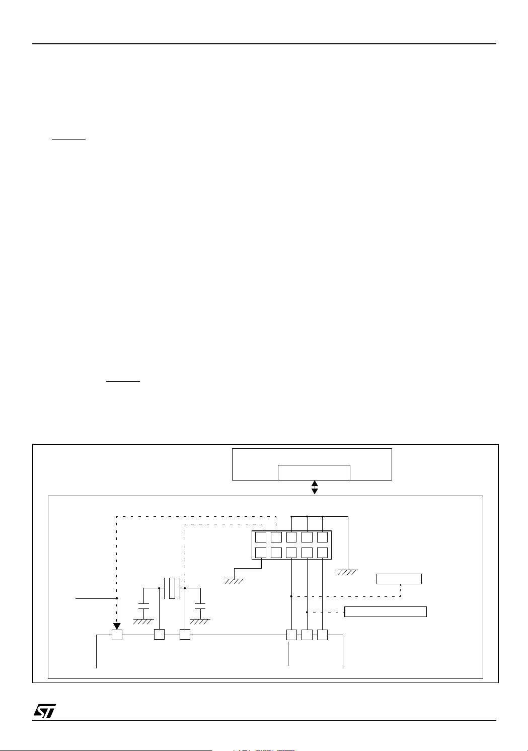
Figure 1. General Block Diagram
PLL
8MHz -> 32MHz
Int.
1% RC
CLKIN
OSC1
OSC2
V
DD
V
SS
RESET
Ext.
OSC
1MHz
to
16MHz
1MHz
PLL x 8
or PLL X4
/ 2
LVD
POWER
SUPPLY
CONTROL
software developers, enabling the design of highly
efficient and compact application code. In addition
to standard 8-bit data management, all ST7 microcontrollers feature true bit manipulation, 8x8 unsigned multiplication and indirect addressing
modes.
For easy reference, all parametric data are located
in section 13 on page 91.The devices feature an
on-chip Debug Module (DM) to support in-circuit
debugging (ICD). For a description of the DM registers, refer to the ST7 ICC Protocol Reference
Manual.
12-Bit
Auto-Reload
TIMER 2
8-Bit
LITE TIMER 2
Internal
CLOCK
PORT A
ADDRESS AND DATA BUS
PORT B
+ OpAmp
ADC
SPI
PA7:0
(8 bits)
PB6:0
(7 bits)
8-BIT CORE
ALU
PROGRAM
MEMORY
(4K Bytes)
RAM
(256 Bytes)
Debug Module
DATA EEPROM
(128 Bytes)
WATCHDOG
5/131
1
Page 6

ST7LITE1
2 PIN DESCRIPTION
Figure 2. 20-Pin SO Package Pinout
V
SS
V
DD
RESET
/AIN0/PB0
SS
SCK/AIN1/PB1
MISO/AIN2/PB2
MOSI/AIN3/PB3
CLKIN/AIN4/PB4
AIN5/PB5
AIN6/PB6
1
2
3
4
5
6
7
8
9
10
ei3
ei2
ei0
ei1
OSC1/CLKIN
20
OSC2
19
PA0 (HS)/LTIC
18
PA1 (HS)/ATIC
17
PA2 (HS)/ATPWM0
16
PA3 (HS)/ATPWM1
15
PA4 (HS)/ATPWM2
14
PA5 (HS)/ATPWM3/ICCDATA
13
PA6/MCO/ICCCLK/BREAK
12
PA7(HS)
11
(HS) 20mA high sink capability
eix associated external interrupt vector
6/131
1
Page 7

ST7LITE1
PIN DESCRIPTION (Cont’d)
Legend / Abbreviations for Table 1:
Type: I = input, O = output, S = supply
In/Output level: C
Output level: HS = 20mA high sink (on N-buffer only)
Port and control configuration:
– Input: float = floating, wpu = weak pull-up, int = interrupt, ana = analog
– Output: OD = open drain, PP = push-pull
The RESET configuration of each pin is shown in bold which is valid as long as the device is in reset state.
Table 1. Device Pin Description
= CMOS 0.3VDD/0.7VDD with input trigger
T
Pin
No.
1V
2V
3 RESET
4 PB0/AIN0/SS
Pin Name
SS
DD
I/O C
Type
S Ground
S Main power supply
I/O C
5 PB1/AIN1/SCK I/O C
6 PB2/AIN2/MISO I/O C
7 PB3/AIN3/MOSI I/O C
8 PB4/AIN4/CLKIN I/O C
9 PB5/AIN5 I/O C
10 PB6/AIN6 I/O C
11 PA7 I/O C
Level Port / Control
Input Output
Input
T
T
Output
float
X
wpu
int
ana
OD
PP
X X Top priority non maskable interrupt (active low)
XXXPort B0
ei3
X XXXPort B1
T
X XXXPort B2
T
X
T
ei2
X XXXPort B4
T
X XXXPort B5 ADC Analog Input 5
T
X XXXPort B6 ADC Analog Input 6
T
HS X ei1 X X Port A7
T
XXXPort B3
Main
Function
(after reset)
Alternate Function
ADC Analog Input 0 or SPI
Slave Select (active low)
Caution: No negative current
injection allowed on this pin. For
details, refer to section 13.2.2
on page 92
ADC Analog Input 1 or SPI Serial Clock
Caution: No negative current
injection allowed on this pin. For
details, refer to section 13.2.2
on page 92
ADC Analog Input 2 or SPI Master In/ Slave Out Data
ADC Analog Input 3 or SPI Master Out / Slave In Data
ADC Analog Input 4 or External
clock input
7/131
1
Page 8

ST7LITE1
Level Port / Control
Pin
No.
Pin Name
Type
Input Output
Input
Output
float
wpu
int
ana
OD
Main
Function
(after reset)
PP
Alternate Function
Main Clock Output or In Circuit
Communication Clock or External BREAK
Caution: During normal operation this pin must be pulled- up,
PA6 /MCO/
12
ICCCLK/BREAK
I/O C
X ei1 XXPort A6
T
internally or externally (external
pull-up of 10k mandatory in
noisy environment). This is to
avoid entering ICC mode unexpectedly during a reset. In the
application, even if the pin is
configured as output, any reset
will put it back in input pull-up
PA5 /
13
ICCDATA
I/O C
14 PA4 I/O C
15 PA3/ATPWM1 I/O C
16 PA2/ATPWM0 I/O C
17 PA1/ATIC I/O C
18 PA0/LTIC I/O C
HS X
T
HS X XXPort A4
T
HS X
T
HS X XXPort A2 Auto-Reload Timer PWM0
T
ei1
ei0
HS X XXPort A1
T
HS X XXPort A0 Lite Timer Input Capture
T
XXPort A5 In Circuit Communication Data
XXPort A3 Auto-Reload Timer PWM1
Auto-Reload Timer Input Capture
19 OSC2 O Resonator oscillator inverter output
20 OSC1/CLKIN I
Resonator oscillator inverter input or External
clock input
8/131
1
Page 9

3 REGISTER & MEMORY MAP
ST7LITE1
As shown in Figure 3, the MCU is capable of addressing 64K bytes of memories and I/O registers.
The available memory locations consist of 128
bytes of register locations, 256 bytes of RAM, 128
bytes of data EEPROM and 4 Kbytes of flash program memory. The RAM space includes up to 128
bytes for the stack from 180h to 1FFh.
The highest address bytes contain the user reset
and interrupt vectors.
Figure 3. Memory Map
0000h
007Fh
0080h
00FFh
0100h
017Fh
0180h
01FFh
0200h
0FFFh
1000h
107Fh
1080h
EFFFh
F000h
FFDFh
FFE0h
FFFFh
HW Registers
(see Table 2)
RAM
(128 Bytes)
Reserved
RAM
(128 Bytes)
Reserved
Data EEPROM
(128 Bytes)
Reserved
Flash Memory
(4K)
Interrupt & Reset Vectors
(see Table 5)
F000h
FBFFh
FC00h
FFFFh
0080h
00FFh
0100h
017Fh
0180h
01FFh
The Flash memory contains two sectors (see Fig-
ure 3) mapped in the upper part of the ST7 ad-
dressing space so the reset and interrupt vectors
are located in Sector 0 (F000h-FFFFh).
The size of Flash Sector 0 and other device options are configurable by Option byte (refer to sec-
tion 15.1 on page 121).
IMPORTANT: Memory locations marked as “Reserved” must never be accessed. Accessing a reseved area can have unpredictable effects on the
device.
Short Addressing
RAM (zero page)
Reserved
128 Bytes Stack
1000h
1001h
see section 7.1 on page 23
4K FLASH
PROGRAM MEMORY
3 Kbytes
SECTOR 1
1 Kbyte
SECTOR 0
FFDEh
FFDFh
see section 7.1 on page 23
RCCR0
RCCR1
RCCR0
RCCR1
9/131
1
Page 10

ST7LITE1
Table 2. Hardware Register Map
Address Block Register Label Register Name Reset Status Remarks
0000h
0001h
0002h
0003h
0004h
0005h
0006h
0007h
0008h
0009h
000Ah
000Bh
000Ch
000Dh
000Eh
000Fh
0010h
0011h
0012h
0013h
0014h
0015h
0016h
0017h
0018h
0019h
001Ah
001Bh
001Ch
001Dh
001Eh
001Fh
0020h
0021h
0022h
Port A
Port B
LITE
TIMER 2
AUTO-
RELOAD
TIMER 2
PADR
PADDR
PAOR
PBDR
PBDDR
PBOR
LTCSR2
LTARR
LTCNTR
LTCSR1
LTICR
ATCSR
CNTRH
CNTRL
ATRH
ATRL
PWMCR
PWM0CSR
PWM1CSR
PWM2CSR
PWM3CSR
DCR0H
DCR0L
DCR1H
DCR1L
DCR2H
DCR2L
DCR3H
DCR3L
ATICRH
ATICRL
TRANCR
BREAKCR
Port A Data Register
Port A Data Direction Register
Port A Option Register
Port B Data Register
Port B Data Direction Register
Port B Option Register
Reserved Area (2 bytes)
Lite Timer Control/Status Register 2
Lite Timer Auto-reload Register
Lite Timer Counter Register
Lite Timer Control/Status Register 1
Lite Timer Input Capture Register
Timer Control/Status Register
Counter Register High
Counter Register Low
Auto-Reload Register High
Auto-Reload Register Low
PWM Output Control Register
PWM 0 Control/Status Register
PWM 1 Control/Status Register
PWM 2 Control/Status Register
PWM 3 Control/Status Register
PWM 0 Duty Cycle Register High
PWM 0 Duty Cycle Register Low
PWM 1 Duty Cycle Register High
PWM 1 Duty Cycle Register Low
PWM 2 Duty Cycle Register High
PWM 2 Duty Cycle Register Low
PWM 3 Duty Cycle Register High
PWM 3 Duty Cycle Register Low
Input Capture Register High
Input Capture Register Low
Transfer Control Register
Break Control Register
1)
FFh
00h
40h
1)
FFh
00h
00h
0Fh
00h
00h
0X00 0000h
xxh
0X00 0000h
00h
00h
00h
00h
00h
00h
00h
00h
00h
00h
00h
00h
00h
00h
00h
00h
00h
00h
00h
01h
00h
R/W
R/W
R/W
R/W
R/W
2)
R/W
R/W
R/W
Read Only
R/W
Read Only
R/W
Read Only
Read Only
R/W
R/W
R/W
R/W
R/W
R/W
R/W
R/W
R/W
R/W
R/W
R/W
R/W
R/W
R/W
Read Only
Read Only
R/W
R/W
0023h to
002Dh
002Eh WDG WDGCR Watchdog Control Register 7Fh R/W
0002Fh FLASH FCSR Flash Control/Status Register 00h R/W
00030h EEPROM EECSR Data EEPROM Control/Status Register 00h R/W
0031h
0032h
0033h
0034h
0035h
0036h
10/131
SPI
ADC
SPIDR
SPICR
SPICSR
ADCCSR
ADCDRH
ADCDRL
SPI Data I/O Register
SPI Control Register
SPI Control Status Register
A/D Control Status Register
A/D Data Register High
A/D Amplifier Control/Data Low Register
Reserved area (11 bytes)
xxh
0xh
00h
00h
xxh
0xh
1
R/W
R/W
R/W
R/W
Read Only
R/W
Page 11

ST7LITE1
Address Block Register Label Register Name Reset Status Remarks
0037h ITC EICR External Interrupt Control Register 00h R/W
0038h MCC MCCSR Main Clock Control/Status Register 00h R/W
0039h
003Ah
003Bh Reserved area (1 byte)
003Ch ITC EISR External Interrupt Selection Register 0Ch R/W
003Dh to
0048h
0049h
004Ah
004Bh
004Ch
004Dh
004Eh
004Fh
0050h
0051h to
007Fh
Clock and
Reset
AWU
3)
DM
RCCR
SICSR
AWUPR
AWUCSR
DMCR
DMSR
DMBK1H
DMBK1L
DMBK2H
DMBK2L
RC oscillator Control Register
System Integrity Control/Status Register
Reserved area (12 bytes)
AWU Prescaler Register
AWU Control/Status Register
DM Control Register
DM Status Register
DM Breakpoint Register 1 High
DM Breakpoint Register 1 Low
DM Breakpoint Register 2 High
DM Breakpoint Register 2 Low
Reserved area (47 bytes)
FFh
0000 0XX0h
FFh
00h
00h
00h
00h
00h
00h
00h
R/W
R/W
R/W
R/W
R/W
R/W
R/W
R/W
R/W
R/W
Legend: x=undefined, R/W=read/write
Notes:
1. The contents of the I/O port DR registers are readable only in output configuration. In input configuration, the values of the I/O pins are returned instead of the DR register contents.
2. The bits associated with unavailable pins must always keep their reset value.
3. For a description of the Debug Module registers, see ICC reference manual.
11/131
1
Page 12

ST7LITE1
4 FLASH PROGRAM MEMORY
4.1 Introduction
The ST7 single voltage extended Flash (XFlash) is
a non-volatile memory that can be electrically
erased and programmed either on a byte-by-byte
basis or up to 32 bytes in parallel.
The XFlash devices can be programmed off-board
(plugged in a programming tool) or on-board using
In-Circuit Programming or In-Application Programming.
The array matrix organisation allows each sector
to be erased and reprogrammed without affecting
other sectors.
4.2 Main Features
■ ICP (In-Circuit Programming)
■ IAP (In-Application Programming)
■ ICT (In-Circuit Testing) for downloading and
executing user application test patterns in RAM
■ Sector 0 size configurable by option byte
■ Read-out and write protection
4.3 PROGRAMMING MODES
The ST7 can be programmed in three different
ways:
– Insertion in a programming tool. In this mode,
FLASH sectors 0 and 1, option byte row and
data EEPROM (if present) can be programmed or erased.
– In-Circuit Programming. In this mode, FLASH
sectors 0 and 1, option byte row and data
EEPROM (if present) can be programmed or
erased without removing the device from the
application board.
– In-Application Programming. In this mode,
sector 1 and data EEPROM (if present) can
be programmed or erased without removing
the device from the application board and
while the application is running.
4.3.1 In-Circuit Programming (ICP)
ICP uses a protocol called ICC (In-Circuit Communication) which allows an ST7 plugged on a printed circuit board (PCB) to communicate with an external programming device connected via cable.
ICP is performed in three steps:
Switch the ST7 to ICC mode (In-Circuit Communications). This is done by driving a specific signal
sequence on the ICCCLK/DATA pins while the
RESET pin is pulled low. When the ST7 enters
ICC mode, it fetches a specific RESET vector
which points to the ST7 System Memory containing the ICC protocol routine. This routine enables
the ST7 to receive bytes from the ICC interface.
– Download ICP Driver code in RAM from the
ICCDATA pin
– Execute ICP Driver code in RAM to program
the FLASH memory
Depending on the ICP Driver code downloaded in
RAM, FLASH memory programming can be fully
customized (number of bytes to program, program
locations, or selection of the serial communication
interface for downloading).
4.3.2 In Application Programming (IAP)
This mode uses an IAP Driver program previously
programmed in Sector 0 by the user (in ICP
mode).
This mode is fully controlled by user software. This
allows it to be adapted to the user application, (user-defined strategy for entering programming
mode, choice of communications protocol used to
fetch the data to be stored etc).
IAP mode can be used to program any memory areas except Sector 0, which is write/erase protected to allow recovery in case errors occur during
the programming operation.
12/131
1
Page 13
FLASH PROGRAM MEMORY (Cont’d)
ST7LITE1
4.4 ICC interface
ICP needs a minimum of 4 and up to 6 pins to be
connected to the programming tool. These pins
are:
– RESET
–V
: device reset
: device power supply ground
SS
– ICCCLK: ICC output serial clock pin
– ICCDATA: ICC input serial data pin
– OSC1: main clock input for external source
(not required on devices without OSC1/OSC2
pins)
: application board power supply (option-
–V
DD
al, see Note 3)
Notes:
1. If the ICCCLK or ICCDATA pins are only used
as outputs in the application, no signal isolation is
necessary. As soon as the Programming Tool is
plugged to the board, even if an ICC session is not
in progress, the ICCCLK and ICCDATA pins are
not available for the application. If they are used as
inputs by the application, isolation such as a serial
resistor has to be implemented in case another device forces the signal. Refer to the Programming
Tool documentation for recommended resistor values.
2. During the ICP session, the programming tool
must control the RESET
pin. This can lead to conflicts between the programming tool and the application reset circuit if it drives more than 5mA at
high level (push pull output or pull-up resistor<1K).
A schottky diode can be used to isolate the application RESET circuit in this case. When using a
classical RC network with R>1K or a reset management IC with open drain output and pull-up resistor>1K, no additional components are needed.
In all cases the user must ensure that no external
reset is generated by the application during the
ICC session.
3. The use of Pin 7 of the ICC connector depends
on the Programming Tool architecture. This pin
must be connected when using most ST Programming Tools (it is used to monitor the application
power supply). Please refer to the Programming
Tool manual.
4. Pin 9 has to be connected to the OSC1 pin of
the ST7 when the clock is not available in the application or if the selected clock option is not programmed in the option byte. ST7 devices with multi-oscillator capability need to have OSC2 grounded in this case.
5. With the ICP option disabled with ST7 MDT10EPB that the external clock has to be provided on
PB4.
Caution: During normal operation the ICCCLK pin
must be pulled- up, internally or externally (external pull-up of 10k mandatory in noisy environment). This is to avoid entering ICC mode unexpectedly during a reset. In the application, even if
the pin is configured as output, any reset will put it
back in input pull-up.
Figure 4. Typical ICC Interface
(See Note 3)
APPLICATION
POWER SUPPLY
C
L2
VDD
OSC2
OPTIONAL
(See Note 4)
C
CLKIN
OSC1/PB4
(See Note 5)
PROGRAMMING TOOL
ICC CONNECTOR
ICC Cable
ICC CONNECTOR
HE10 CONNECTOR TYPE
APPLICATION BOARD
APPLICATION
RESET SOURCE
See Note 2
See Note 1 and Caution
APPLICATION
I/O
13/131
RESET
1
246810
ICCCLK
ICCDATA
975 3
L1
ST7
1
Page 14

ST7LITE1
FLASH PROGRAM MEMORY (Cont’d)
4.5 Memory Protection
There are two different types of memory protection: Read Out Protection and Write/Erase Protection which can be applied individually.
4.5.1 Read out Protection
Readout protection, when selected provides a protection against program memory content extraction and against write access to Flash memory.
Even if no protection can be considered as totally
unbreakable, the feature provides a very high level
of protection for a general purpose microcontroller.
Both program and data E
2
memory are protected.
In flash devices, this protection is removed by reprogramming the option. In this case, both program and data E
2
memory are automatically
erased and the device can be reprogrammed.
Read-out protection selection depends on the de-
vice type:
– In Flash devices it is enabled and removed
through the FMP_R bit in the option byte.
– In ROM devices it is enabled by mask option
specified in the Option List.
4.5.2 Flash Write/Erase Protection
Write/erase protection, when set, makes it impossible to both overwrite and erase program memory. It does not apply to E
2
data. Its purpose is to
provide advanced security to applications and prevent any change being made to the memory content.
Warning: Once set, Write/erase protection can
never be removed. A write-protected flash device
is no longer reprogrammable.
Write/erase protection is enabled through the
FMP_W bit in the option byte.
4.6 Related Documentation
For details on Flash programming and ICC protocol, refer to the ST7 Flash Programming Reference Manual and to the ST7 ICC Protocol Reference Manual
.
4.7 Register Description
FLASH CONTROL/STATUS REGISTER (FCSR)
Read/Write
Reset Value: 000 0000 (00h)
1st RASS Key: 0101 0110 (56h)
2nd RASS Key: 1010 1110 (AEh)
70
00000OPTLATPGM
Note: This register is reserved for programming
using ICP, IAP or other programming methods. It
controls the XFlash programming and erasing operations.
When an EPB or another programming tool is
used (in socket or ICP mode), the RASS keys are
sent automatically.
14/131
1
Page 15

5 DATA EEPROM
ST7LITE1
5.1 INTRODUCTION
The Electrically Erasable Programmable Read
Only Memory can be used as a non volatile backup for storing data. Using the EEPROM requires a
basic access protocol described in this chapter.
Figure 5. EEPROM Block Diagram
EECSR
ADDRESS
DECODER
0 E2LAT00 0 0 0 E2PGM
4
DECODER
ROW
5.2 MAIN FEATURES
■ Up to 32 Bytes programmed in the same cycle
■ EEPROM mono-voltage (charge pump)
■ Chained erase and programming cycles
■ Internal control of the global programming cycle
duration
■ WAIT mode management
■ Readout protection
HIGH VOLTAGE
PUMP
EEPROM
MEMORY MATRIX
(1 ROW = 32 x 8 BITS)
ADDRESS BUS
128128
4
4
DATA
MULTIPLEXER
DATA BUS
32 x 8 BITS
DATA LATCHES
15/131
1
Page 16

ST7LITE1
DATA EEPROM (Cont’d)
5.3 MEMORY ACCESS
The Data EEPROM memory read/write access
modes are controlled by the E2LAT bit of the EEPROM Control/Status register (EECSR). The flowchart in Figure 6 describes these different memory
access modes.
Read Operation (E2LAT=0)
The EEPROM can be read as a normal ROM location when the E2LAT bit of the EECSR register is
cleared. In a read cycle, the byte to be accessed is
put on the data bus in less than 1 CPU clock cycle.
This means that reading data from EEPROM
takes the same time as reading data from
EPROM, but this memory cannot be used to execute machine code.
Write Operation (E2LAT=1)
To access the write mode, the E2LAT bit has to be
set by software (the E2PGM bit remains cleared).
When a write access to the EEPROM area occurs,
Figure 6. Data EEPROM Programming Flowchart
the value is latched inside the 32 data latches according to its address.
When PGM bit is set by the software, all the previous bytes written in the data latches (up to 32) are
programmed in the EEPROM cells. The effective
high address (row) is determined by the last EEPROM write sequence. To avoid wrong programming, the user must take care that all the bytes
written between two programming sequences
have the same high address: only the five Least
Significant Bits of the address can change.
At the end of the programming cycle, the PGM and
LAT bits are cleared simultaneously.
Note: Care should be taken during the programming cycle. Writing to the same memory location
will over-program the memory (logical AND between the two write access data result) because
the data latches are only cleared at the end of the
programming cycle and by the falling edge of the
E2LAT bit.
It is not possible to read the latched data.
This note is ilustrated by the Figure 8.
READ MODE
E2LAT=0
E2PGM=0
READ BYTES
IN EEPROM AREA
CLEARED BY HARDWARE
WRITE MODE
E2LAT=1
E2PGM=0
WRITEUPTO32BYTES
IN EEPROM AREA
(with the same 11 MSB of the address)
START PROGRAMMING CYCLE
E2LAT=1
E2PGM=1 (set by software)
01
E2LAT
16/131
1
Page 17

DATA EEPROM (Cont’d)
2
Figure 7. Data E
DEFINITION
PROM Write Operation
⇓ Row / Byte ⇒ 0 1 2 3 ... 30 31 Physical Address
ROW
ST7LITE1
0
1
...
N
00h...1Fh
20h...3Fh
Nx20h...Nx20h+1Fh
E2LAT bit
E2PGM bit
Read operation impossible
Byte 1 Byte 2 Byte 32
PHASE 1
Writing data latches Waiting E2PGM and E2LAT to fall
Set by USER application
Programming cycle
PHASE 2
Read operation possible
Cleared by hardware
Note: If a programming cycle is interrupted (by software or a reset action), the integrity of the data in mem-
ory is not guaranteed.
17/131
1
Page 18

ST7LITE1
DATA EEPROM (Cont’d)
5.4 POWER SAVING MODES
Wait mode
The DATA EEPROM can enter WAIT mode on execution of the WFI instruction of the microcontroller or when the microcontroller enters Active-HALT
mode.The DATA EEPROM will immediately enter
this mode if there is no programming in progress,
otherwise the DATA EEPROM will finish the cycle
and then enter WAIT mode.
Active-Halt mode
Refer to Wait mode.
Halt mode
The DATA EEPROM immediately enters HALT
mode if the microcontroller executes the HALT instruction. Therefore the EEPROM will stop the
function in progress, and data may be corrupted.
5.5 ACCESS ERROR HANDLING
If a read access occurs while E2LAT=1, then the
data bus will not be driven.
If a write access occurs while E2LAT=0, then the
data on the bus will not be latched.
If a programming cycle is interrupted (by software/
RESET action), the memory data will not be guaranteed.
5.6 Data EEPROM Read-out Protection
The read-out protection is enabled through an option bit (see section 15.1 on page 121).
When this option is selected, the programs and
data stored in the EEPROM memory are protected
against read-out (including a re-write protection).
In Flash devices, when this protection is removed
by reprogramming the Option Byte, the entire Program memory and EEPROM is first automatically
erased.
Note: Both Program Memory and data EEPROM
are protected using the same option bit.
Figure 8. Data EEPROM Programming Cycle
READ OPERATION NOT POSSIBLE
INTERNAL
PROGRAMMING
VOLTAGE
ERASE CYCLE WRITE CYCLE
WRITE OF
DATA LATCHES
t
PROG
READ OPERATION POSSIBLE
LAT
PGM
18/131
1
Page 19

DATA EEPROM (Cont’d)
5.7 REGISTER DESCRIPTION
EEPROM CONTROL/STATUS REGISTER (EECSR)
Read/Write
Reset Value: 0000 0000 (00h)
70
000000E2LATE2PGM
Bits 7:2 = Reserved, forced by hardware to 0.
Bit 1 = E2LAT Latch Access Transfer
This bit is set by software. It is cleared by hardware at the end of the programming cycle. It can
only be cleared by software if the E2PGM bit is
cleared.
0: Read mode
1: Write mode
ST7LITE1
Bit 0 = E2PGM Programming control and status
This bit is set by software to begin the programming
cycle. At the end of the programming cycle, this bit
is cleared by hardware.
0: Programming finished or not yet started
1: Programming cycle is in progress
Note: if the E2PGM bit is cleared during the programming cycle, the memory data is not guaranteed
Table 3. DATA EEPROM Register Map and Reset Values
Address
(Hex.)
0030h
Register
Label
EECSR
Reset Value
76543210
000000
E2LAT0E2PGM
0
19/131
1
Page 20

ST7LITE1
6 CENTRAL PROCESSING UNIT
6.1 INTRODUCTION
This CPU has a full 8-bit architecture and contains
six internal registers allowing efficient 8-bit data
manipulation.
6.2 MAIN FEATURES
■ 63 basic instructions
■ Fast 8-bit by 8-bit multiply
■ 17 main addressing modes
■ Two 8-bit index registers
■ 16-bit stack pointer
■ Low power modes
■ Maskable hardware interrupts
■ Non-maskable software interrupt
6.3 CPU REGISTERS
The 6 CPU registers shown in Figure 9 are not
present in the memory mapping and are accessed
by specific instructions.
Figure 9. CPU Registers
70
RESET VALUE = XXh
70
RESET VALUE = XXh
70
RESET VALUE = XXh
Accumulator (A)
The Accumulator is an 8-bit general purpose register used to hold operands and the results of the
arithmetic and logic calculations and to manipulate
data.
Index Registers (X and Y)
In indexed addressing modes, these 8-bit registers
are used to create either effective addresses or
temporary storage areas for data manipulation.
(The Cross-Assembler generates a precede instruction (PRE) to indicate that the following instruction refers to the Y register.)
The Y register is not affected by the interrupt automatic procedures (not pushed to and popped from
the stack).
Program Counter (PC)
The program counter is a 16-bit register containing
the address of the next instruction to be executed
by the CPU. It is made of two 8-bit registers PCL
(Program Counter Low which is the LSB) and PCH
(Program Counter High which is the MSB).
ACCUMULATOR
X INDEX REGISTER
Y INDEX REGISTER
15 8
RESET VALUE = RESET VECTOR @ FFFEh-FFFFh
15
RESET VALUE = STACK HIGHER ADDRESS
20/131
PCH
RESET VALUE =
7
70
1C11HI NZ
1X11X1XX
70
8
PCL
1
0
PROGRAM COUNTER
CONDITION CODE REGISTER
STACK POINTER
X = Undefined Value
Page 21

CPU REGISTERS (Cont’d)
CONDITION CODE REGISTER (CC)
Read/Write
Reset Value: 111x1xxx
70
111HINZC
because the I bit is set by hardware at the start of
the routine and reset by the IRET instruction at the
end of the routine. If the I bit is cleared by software
in the interrupt routine, pending interrupts are
serviced regardless of the priority level of the current interrupt routine.
Bit 2 = N Negative.
The 8-bit Condition Code register contains the interrupt mask and four flags representative of the
result of the instruction just executed. This register
can also be handled by the PUSH and POP instructions.
These bits can be individually tested and/or controlled by specific instructions.
This bit is set and cleared by hardware. It is repre-
sentative of the result sign of the last arithmetic,
logical or data manipulation. It is a copy of the 7
bit of the result.
0: The result of the last operation is positive or null.
1: The result of the last operation is negative
(i.e. the most significant bit is a logic 1).
This bit is accessed by the JRMI and JRPL instrucBit 4 = H Half carry.
tions.
This bit is set by hardware when a carry occurs be-
tween bits 3 and 4 of the ALU during an ADD or
ADC instruction. It is reset by hardware during the
same instructions.
0: No half carry has occurred.
1: A half carry has occurred.
This bit is tested using the JRH or JRNH instruction. The H bit is useful in BCD arithmetic subroutines.
Bit 1 = Z Zero.
This bit is set and cleared by hardware. This bit in-
dicates that the result of the last arithmetic, logical
or data manipulation is zero.
0: The result of the last operation is different from
zero.
1: The result of the last operation is zero.
This bit is accessed by the JREQ and JRNE test
instructions.
Bit 3 = I Interrupt mask.
This bit is set by hardware when entering in interrupt or by software to disable all interrupts except
the TRAP software interrupt. This bit is cleared by
software.
0: Interrupts are enabled.
1: Interrupts are disabled.
This bit is controlled by the RIM, SIM and IRET instructions and is tested by the JRM and JRNM instructions.
Note: Interrupts requested while I is set are
latched and can be processed when I is cleared.
Bit 0 = C Carry/borrow.
This bit is set and cleared by hardware and soft-
ware. It indicates an overflow or an underflow has
occurred during the last arithmetic operation.
0: No overflow or underflow has occurred.
1: An overflow or underflow has occurred.
This bit is driven by the SCF and RCF instructions
and tested by the JRC and JRNC instructions. It is
also affected by the “bit test and branch”, shift and
rotate instructions.
By default an interrupt routine is not interruptable
ST7LITE1
th
21/131
1
Page 22

ST7LITE1
CPU REGISTERS (Cont’d)
STACK POINTER (SP)
Read/Write
Reset Value: 01FFh
15 8
00000001
70
1 SP6 SP5 SP4 SP3 SP2 SP1 SP0
The Stack Pointer is a 16-bit register which is always pointing to the next free location in the stack.
It is then decremented after data has been pushed
onto the stack and incremented before data is
popped from the stack (see Figure 10).
Since the stack is 128 bytes deep, the 9 most significant bits are forced by hardware. Following an
MCU Reset, or after a Reset Stack Pointer instruction (RSP), the Stack Pointer contains its reset value (the SP6 to SP0 bits are set) which is the stack
higher address.
The least significant byte of the Stack Pointer
(called S) can be directly accessed by a LD instruction.
Note: When the lower limit is exceeded, the Stack
Pointer wraps around to the stack upper limit, with-
out indicating the stack overflow. The previously
stored information is then overwritten and there-
fore lost. The stack also wraps in case of an under-
flow.
The stack is used to save the return address dur-
ing a subroutine call and the CPU context during
an interrupt. The user may also directly manipulate
the stack by means of the PUSH and POP instruc-
tions. In the case of an interrupt, the PCL is stored
at the first location pointed to by the SP. Then the
other registers are stored in the next locations as
shown in Figure 10.
– When an interrupt is received, the SP is decre-
mented and the context is pushed on the stack.
– On return from interrupt, the SP is incremented
and the context is popped from the stack.
A subroutine call occupies two locations and an in-
terrupt five locations in the stack area.
Figure 10. Stack Manipulation Example
@ 0180h
SP
@ 01FFh
CALL
Subroutine
SP
PCH
PCL
Stack Higher Address = 01FFh
Stack Lower Address =
Interrupt
Event
SP
CC
A
X
PCH
PCL
PCH
PCL
0180h
PUSH Y POP Y IRET
SP
Y
CC
A
X
PCH
PCL
PCH
PCL
CC
A
X
PCH
PCL
PCH
PCL
SP
PCH
PCL
RET
or RSP
SP
22/131
1
Page 23

7 SUPPLY, RESET AND CLOCK MANAGEMENT
ST7LITE1
The device includes a range of utility features for
securing the application in critical situations (for
example in case of a power brown-out), and reducing the number of external components.
Main features
■ Clock Management
– 1 MHz internal RC oscillator (enabled by op-
tion byte, available on ST7LITE15 and
ST7LITE19 devices only)
– 1 to 16 MHz or 32kHz External crystal/ceramic
resonator (selected by option byte)
– External Clock Input (enabled by option byte)
– PLL for multiplying the frequency by 8 or 4
(enabled by option byte)
– For clock ART counter only: PLL32 for multi-
plying the 8 MHz frequency by 4 (enabled by
option byte). The 8 MHz input frequency is
mandatory and can be obtained in the follow-
ing ways:
–1 MHz RC + PLLx8
–16 MHz external clock (internally divided
by 2)
–2 MHz. external clock (internally divided by
2) + PLLx8
–Crystal oscillator with 16 MHz output fre-
quency (internally divided by 2)
■ Reset Sequence Manager (RSM)
■ System Integrity Management (SI)
– Main supply Low voltage detection (LVD) with
reset generation (enabled by option byte)
– Auxiliary Voltage detector (AVD) with interrupt
capability for monitoring the main supply (en-
abled by option byte)
7.1 INTERNAL RC OSCILLATOR ADJUSTMENT
The device contains an internal RC oscillator with
an accuracy of 1% for a given device, temperature
and voltage range (4.5V-5.5V). It must be calibrated to obtain the frequency required in the application. This is done by software writing a calibration
value in the RCCR (RC Control Register).
Whenever the microcontroller is reset, the RCCR
returns to its default value (FFh), i.e. each time the
device is reset, the calibration value must be loaded in the RCCR. Predefined calibration values are
stored in EEPROM for 3 and 5V V
ages at 25°C, as shown in the following table.
supply volt-
DD
RCCR Conditions
=5V
V
DD
=25°C
RCCR0
RCCR1
T
A
=1MHz
f
RC
=3V
V
DD
=25°C
T
A
=700KHz
f
RC
ST7LITE19
Address
1000h
and FFDEh
1001h
and FFDFh
ST7LITE15
Address
FFDEh
FFDFh
Note:
– See “ELECTRICAL CHARACTERISTICS” on
page 91. for more information on the frequency
and accuracy of the RC oscillator.
– To improve clock stability, it is recommended to
place a decoupling capacitor between the V
SS
pins.
and V
DD
– These two bytes are systematically programmed
by ST, including on FASTROM devices. Consequently, customers intending to use FASTROM
service must not use these two bytes.
– RCCR0 and RCCR1 calibration values will be
erased if the read-out protection bit is reset after
it has been set. See “Read out Protection” on
page 14.
Caution: If the voltage or temperature conditions
change in the application, the frequency may need
to be recalibrated.
Refer to application note AN1324 for information
on how to calibrate the RC frequency using an external reference signal.
7.2 PHASE LOCKED LOOP
The PLL can be used to multiply a 1MHz frequency from the RC oscillator or the external clock by 4
or 8 to obtain f
of 4 or 8 MHz. The PLL is ena-
OSC
bled and the multiplication factor of 4 or 8 is selected by 2 option bits.
– The x4 PLL is intended for operation with V
DD
in
the 2.4V to 3.3V range
– The x8 PLL is intended for operation with V
DD
in
the 3.3V to 5.5V range
Refer to Section 15.1 for the option byte description.
If the PLL is disabled and the RC oscillator is enabled, then f
OSC =
1MHz.
If both the RC oscillator and the PLL are disabled,
is driven by the external clock.
f
OSC
23/131
1
Page 24

ST7LITE1
PHASE LOCKED LOOP (Cont’d)
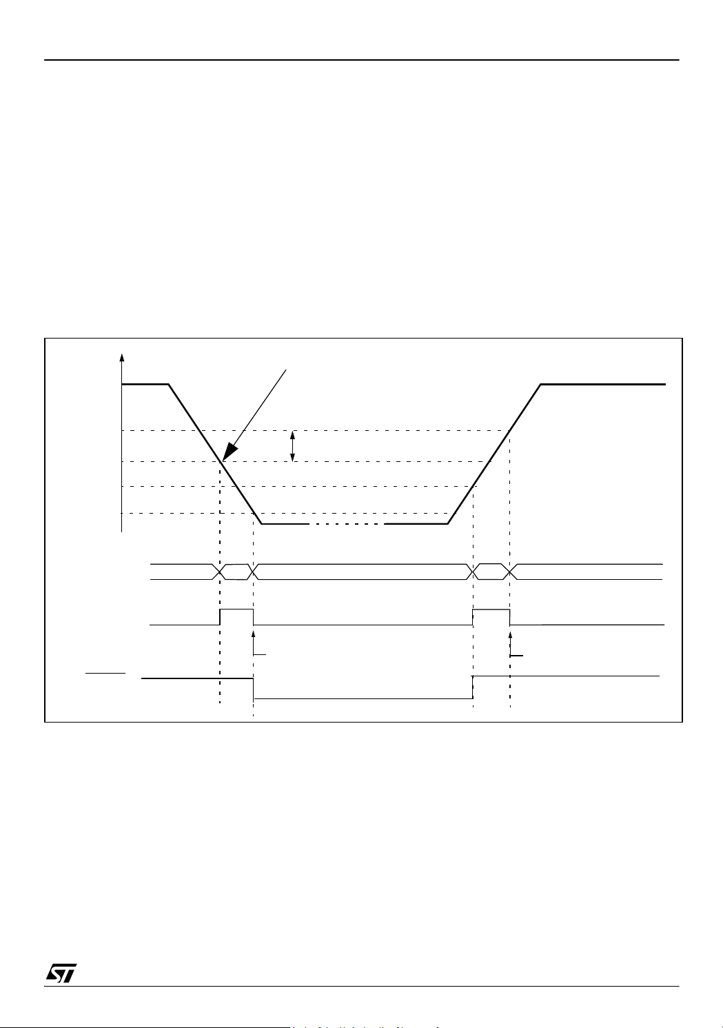
Figure 11. PLL Output Frequency Timing
Diagram
LOCKED bit set
4/8 x
input
freq.
t
STAB
t
LOCK
t
STARTUP
Output freq.
t
When the PLL is started, after reset or wakeup
from Halt mode or AWUFH mode, it outputs the
clock after a delay of t
STARTUP
.
When the PLL output signal reaches the operating
frequency, the LOCKED bit in the SICSCR register
is set. Full PLL accuracy (ACC
a stabilization time of t
STAB
) is reached after
PLL
(see Figure 11 and
13.3.4 Internal RC Oscillator and PLL)
Refer to section 7.6.4 on page 33 for a description
of the LOCKED bit in the SICSR register.
7.3 REGISTER DESCRIPTION
MAIN CLOCK CONTROL/STATUS REGISTER
(MCCSR)
Read / Write
Reset Value: 0000 0000 (00h)
70
000000
MCO SMS
Bits 7:2 = Reserved, must be kept cleared.
Bit 1 = MCO Main Clock Out enable
This bit is read/write by software and cleared by
hardware after a reset. This bit allows to enable
the MCO output clock.
0: MCO clock disabled, I/O port free for general
purpose I/O.
1: MCO clock enabled.
Bit 0 = SMS Slow Mode select
This bit is read/write by software and cleared by
hardware after a reset. This bit selects the input
OSC
or f
clock f
0: Normal mode (f
1: Slow mode (f
/32.
OSC
CPU = fOSC
CPU = fOSC
/32)
24/131
RC CONTROL REGISTER (RCCR)
Read / Write
Reset Value: 1111 1111 (FFh)
70
CR
CR70 CR60 CR50 CR40 CR30 CR20 CR10
0
Bits 7:0 = CR[7:0] RC Oscillator Frequency Ad-
justment Bits
These bits must be written immediately after reset
to adjust the RC oscillator frequency and to obtain
an accuracy of 1%. The application can store the
correct value for each voltage range in EEPROM
and write it to this register at start-up.
00h = maximum available frequency
FFh = lowest available frequency
Note: To tune the oscillator, write a series of different values in the register until the correct frequency is reached. The fastest method is to use a dichotomy starting with 80h.
1
Page 25

Figure 12. Clock Management Block Diagram
ST7LITE1
CLKIN
CLKIN
/OSC1
OSC2
OSC,PLLOFF,
OSCRANGE[2:0]
Option bits
CLKIN
CLKIN
OSC
1-16 MHZ
or 32kHz
f
OSC
/32 DIVIDER
CR4CR7 CR0CR1CR2CR3CR6 CR5
Tunable
Oscillator1% RC
f
CPU
PLL 1MHz -> 8MHz
PLL 1MHz -> 4MHz
/2
CLKIN/2
DIVIDER
OSC
/2
DIVIDER
8-BIT
LITE TIMER 2 COUNTER
f
/32
OSC
f
OSC
1
0
RCCR
PLL
8MHz -> 32MHz
(1ms timebase @ 8 MHz f
f
LTIMER
12-BIT
AT TIMER 2
RC OSC
PLLx4x8
CLKIN/2
OSC/2
OSC,PLLOFF,
OSCRANGE[2:0]
Option bits
f
CPU
TO CPU AND
PERIPHERALS
f
OSC
OSC
)
MCO
SMS
MCCSR
f
CPU
MCO
25/131
1
Page 26

ST7LITE1
7.4 MULTI-OSCILLATOR (MO)
The main clock of the ST7 can be generated by
four different source types coming from the multioscillator block (1 to 16MHz or 32kHz):
■ an external source
■ 5 crystal or ceramic resonator oscillators
■ an internal high frequency RC oscillator
Each oscillator is optimized for a given frequency
range in terms of consumption and is selectable
through the option byte. The associated hardware
configurations are shown in Table 4. Refer to the
electrical characteristics section for more details.
External Clock Source
In this external clock mode, a clock signal (square,
sinus or triangle) with ~50% duty cycle has to drive
the OSC1 pin while the OSC2 pin is tied to ground.
Note: when the Multi-Oscillator is not used, PB4 is
selected by default as external clock.
Crystal/Ceramic Oscillators
This family of oscillators has the advantage of producing a very accurate rate on the main clock of
the ST7. The selection within a list of 4 oscillators
with different frequency ranges has to be done by
option byte in order to reduce consumption (refer
to section 15.1 on page 121 for more details on the
frequency ranges). In this mode of the multi-oscillator, the resonator and the load capacitors have
to be placed as close as possible to the oscillator
pins in order to minimize output distortion and
start-up stabilization time. The loading capacitance values must be adjusted according to the
selected oscillator.
These oscillators are not stopped during the
RESET phase to avoid losing time in the oscillator
start-up phase.
Internal RC Oscillator
In this mode, the tunable 1%RC oscillator is used
as main clock source. The two oscillator pins have
to be tied to ground.
Table 4. ST7 Clock Sources
Hardware Configuration
OSC1 OSC2
External ClockCrystal/Ceramic ResonatorsInternal RC Oscillator
EXTERNAL
SOURCE
OSC1 OSC2
C
L1
OSC1 OSC2
ST7
ST7
LOAD
CAPACITORS
ST7
C
L2
26/131
1
Page 27

7.5 RESET SEQUENCE MANAGER (RSM)
ST7LITE1
7.5.1 Introduction
The reset sequence manager includes three RESET sources as shown in Figure 14:
■ External RESET source pulse
■ Internal LVD RESET (Low Voltage Detection)
■ Internal WATCHDOG RESET
These sources act on the RESET
pin and it is al-
ways kept low during the delay phase.
The RESET service routine vector is fixed at ad-
dresses FFFEh-FFFFh in the ST7 memory map.
The basic RESET sequence consists of 3 phases
as shown in Figure 13:
■ Active Phase depending on the RESET source
■ 256 or 4096 CPU clock cycle delay (see table
below)
■ RESET vector fetch
The 256 or 4096 CPU clock cycle delay allows the
oscillator to stabilise and ensures that recovery
has taken place from the Reset state. The shorter
or longer clock cycle delay is automatically selected depending on the clock source chosen by option byte:
Clock Source
Internal RC Oscillator 256
External clock (connected to CLKIN pin) 256
External Crystal/Ceramic Oscillator
(connected to OSC1/OSC2 pins)
CPU clock
cycle delay
4096
The RESET vector fetch phase duration is 2 clock
cycles.
If the PLL is enabled by option byte, it outputs the
clock after an additional delay of t
STARTUP
(see
Figure 11).
Figure 13. RESET Sequence Phases
RESET
Active Phase
INTERNAL RESET
256 or 4096 CLOCK CYCLES
7.5.2 Asynchronous External RESET
The RESET
output with integrated R
pin is both an input and an open-drain
weak pull-up resistor.
ON
FETCH
VECTOR
pin
This pull-up has no fixed value but varies in accordance with the input voltage. It
can be pulled
low by external circuitry to reset the device. See
Electrical Characteristic section for more details.
A RESET signal originating from an external
source must have a duration of at least t
h(RSTL)in
in
order to be recognized (see Figure 15). This detection is asynchronous and therefore the MCU
can enter reset state even in HALT mode.
Figure 14. Reset Block Diagram
V
DD
R
ON
RESET
Filter
PULSE
GENERATOR
INTERNAL
RESET
WATCHDOG RESET
LVD RESET
27/131
1
Page 28

ST7LITE1
RESET SEQUENCE MANAGER (Cont’d)
The RESET
plays a major role in EMS performance. In a noisy
environment, it is recommended to follow the
guidelines mentioned in the electrical characteristics section.
7.5.3 External Power-On RESET
If the LVD is disabled by option byte, to start up the
microcontroller correctly, the user must ensure by
means of an external reset circuit that the reset
signal is held low until V
level specified for the selected f
A proper reset signal for a slow rising V
can generally be provided by an external RC network connected to the RESET
Figure 15. RESET Sequences
pin is an asynchronous signal which
is over the minimum
DD
frequency.
OSC
supply
DD
pin.
V
DD
7.5.4 Internal Low Voltage Detector (LVD) RESET
Two different RESET sequences caused by the internal LVD circuitry can be distinguished:
■ Power-On RESET
■ Voltage Drop RESET
The device RESET
pulled low when V
V
DD<VIT-
(falling edge) as shown in Figure 15.
The LVD filters spikes on V
pin acts as an output that is
DD<VIT+
(rising edge) or
larger than t
DD
g(VDD)
to
avoid parasitic resets.
7.5.5 Internal Watchdog RESET
The RESET sequence generated by a internal
Watchdog counter overflow is shown in Figure 15.
Starting from the Watchdog counter underflow, the
device RESET
low during at least t
pin acts as an output that is pulled
w(RSTL)out
.
V
IT+(LVD)
V
IT-(LVD)
EXTERNAL
RESET
SOURCE
RESET PIN
WATCHDOG
RESET
RUN
LVD
RESET
ACTIVE PHASE
RUN
t
h(RSTL)in
EXTERNAL
RESET
ACTIVE
PHASE
WATCHDOG UNDERFLOW
RUN RUN
INTERNAL RESET (256 or 4096 T
VECTOR FETCH
WATCHDOG
RESET
ACTIVE
PHASE
t
w(RSTL)out
CPU
)
28/131
1
Page 29

7.6 SYSTEM INTEGRITY MANAGEMENT (SI)
ST7LITE1
The System Integrity Management block contains
the Low voltage Detector (LVD) and Auxiliary Voltage Detector (AVD) functions. It is managed by
the SICSR register.
Note: A reset can also be triggered following the
detection of an illegal opcode or prebyte code. Refer to section 12.2.1 on page 88 for further details.
7.6.1 Low Voltage Detector (LVD)
The Low Voltage Detector function (LVD) generates a static reset when the V
below a V
IT-(LVD)
reference value. This means that
supply voltage is
DD
it secures the power-up as well as the power-down
keeping the ST7 in reset.
The V
IT-(LVD)
lower than the V
reference value for a voltage drop is
IT+(LVD)
reference value for poweron in order to avoid a parasitic reset when the
MCU starts running and sinks current on the supply (hysteresis).
The LVD Reset circuitry generates a reset when
is below:
V
DD
–V
–V
IT+(LVD)
IT-(LVD)
when VDD is rising
when VDD is falling
The LVD function is illustrated in Figure 16.
The voltage threshold can be configured by option
byte to be low, medium or high.
Provided the minimum V
the oscillator frequency) is above V
value (guaranteed for
DD
IT-(LVD)
, the
MCU can only be in two modes:
– under full software control
– in static safe reset
In these conditions, secure operation is always ensured for the application without the need for external reset hardware.
During a Low Voltage Detector Reset, the RESET
pin is held low, thus permitting the MCU to reset
other devices.
Notes:
The LVD allows the device to be used without any
external RESET circuitry.
The LVD is an optional function which can be se-
lected by option byte.
It is recommended to make sure that the V
DD
supply voltage rises monotonously when the device is
exiting from Reset, to ensure the application functions properly.
Figure 16. Low Voltage Detector vs Reset
V
DD
V
IT+
(LVD)
V
IT-
(LVD)
RESET
V
hys
29/131
1
Page 30

ST7LITE1
Figure 17. Reset and Supply Management Block Diagram
RESET
V
SS
V
DD
RESET SEQUENCE
MANAGER
(RSM)
WATCHDOG
TIMER (WDG)
STATUS FLAG
SYSTEM INTEGRITY MANAGEMENT
SICSR
00 LVDRFLOCKEDWDGRF0
LOW VOLTAGE
AUXILIARY VOLTAGE
AVD Interrupt Request
AVDIEAVDF
DETECTOR
(LVD)
DETECTOR
(AVD)
30/131
1
Page 31
SYSTEM INTEGRITY MANAGEMENT (Cont’d)
7.6.2 Auxiliary Voltage Detector (AVD)
The Voltage Detector function (AVD) is based on
an analog comparison between a V
V
IT+(AVD)
ply voltage (V
reference value and the VDD main sup-
AVD
). The V
IT-(AVD)
reference value
for falling voltage is lower than the V
IT-(AVD)
IT+(AVD)
and
reference value for rising voltage in order to avoid parasitic detection (hysteresis).
The output of the AVD comparator is directly readable by the application software through a real
time status bit (AVDF) in the SICSR register. This
bit is read only.
Caution: The AVD functions only if the LVD is en-
ST7LITE1
abled through the option byte.
7.6.2.1 Monitoring the V
The AVD voltage threshold value is relative to the
selected LVD threshold configured by option byte
(see section 15.1 on page 121).
If the AVD interrupt is enabled, an interrupt is generated when the voltage crosses the V
V
IT-(AVD)
threshold (AVDF bit is set).
In the case of a drop in voltage, the AVD interrupt
acts as an early warning, allowing software to shut
down safely before the LVD resets the microcontroller. See Figure 18.
Main Supply
DD
IT+(LVD)
or
Figure 18. Using the AVD to Monitor V
V
DD
V
IT+(AVD)
V
IT-(AVD)
V
IT+(LVD)
V
IT-(LVD)
AVDF bit
AVD INTERRUPT
REQUEST
IF AVDIE bit = 1
LVD RESET
01
INTERRUPT Cleared by
DD
Early Warning Interrupt
(Power has dropped, MCU not
not yet in reset)
V
hyst
RESET
reset
01
INTERRUPT Cleared by
hardware
31/131
1
Page 32

ST7LITE1
SYSTEM INTEGRITY MANAGEMENT (Cont’d)
7.6.3 Low Power Modes
Mode Description
WAIT
HALT
7.6.3.1 Interrupts
The AVD interrupt event generates an interrupt if
the corresponding Enable Control Bit (AVDIE) is
No effect on SI. AVD interrupts cause the
device to exit from Wait mode.
The SICSR register is frozen.
The AVD remains active.
set and the interrupt mask in the CC register is reset (RIM instruction).
Flag
Enable
Control
Bit
Interrupt Event
AVD event AVDF AVDIE Yes No
Event
Exit
from
Wait
Exit
from
Halt
32/131
1
Page 33

SYSTEM INTEGRITY MANAGEMENT (Cont’d)
7.6.4 Register Description SYSTEM INTEGRITY (SI) CONTROL/STATUS REGISTER (SICSR)
Read/Write
Reset Value: 0000 0xx0 (0xh)
70
000
WDG
LOCKED LVDRF AVDF AVDIE
RF
Bit 2 = LVDRF LVD reset flag
This bit indicates that the last Reset was generated by the LVD block. It is set by hardware (LVD reset) and cleared by software (by reading). When
the LVD is disabled by OPTION BYTE, the LVDRF
bit value is undefined.
Bit 1 = AVDF Voltage Detector flag
Bit 7:5 = Reserved, must be kept cleared.
This read-only bit is set and cleared by hardware.
If the AVDIE bit is set, an interrupt request is gen-
Bit 4 = WDGRF Watchdog reset flag
This bit indicates that the last Reset was generated by the Watchdog peripheral. It is set by hardware (watchdog reset) and cleared by software
erated when the AVDF bit is set. Refer to Figure
18 and to Section 7.6.2.1 for additional details.
over AVD threshold
0: V
DD
under AVD threshold
1: V
DD
(writing zero) or an LVD Reset (to ensure a stable
cleared state of the WDGRF flag when CPU
starts).
Combined with the LVDRF flag information, the
flag description is given by the following table.
RESET Sources LVDRF WDGRF
External RESET
Watchdog 0 1
LVD 1 X
pin 0 0
Bit 0 = AVDIE Voltage Detector interrupt enable
This bit is set and cleared by software. It enables
an interrupt to be generated when the AVDF flag is
set. The pending interrupt information is automatically cleared when software enters the AVD interrupt routine.
0: AVD interrupt disabled
1: AVD interrupt enabled
ST7LITE1
Bit 3 = LOCKED PLL Locked Flag
This bit is set and cleared by hardware. It is set automatically when the PLL reaches its operating frequency.
0: PLL not locked
1: PLL locked
Application notes
The LVDRF flag is not cleared when another RESET type occurs (external or watchdog), the
LVDRF flag remains set to keep trace of the original failure.
In this case, a watchdog reset can be detected by
software while an external reset can not.
33/131
1
Page 34

ST7LITE1
8 INTERRUPTS
The ST7 core may be interrupted by one of two different methods: maskable hardware interrupts as
listed in the Interrupt Mapping Table and a nonmaskable software interrupt (TRAP). The Interrupt
processing flowchart is shown in Figure 19.
The maskable interrupts must be enabled by
clearing the I bit in order to be serviced. However,
disabled interrupts may be latched and processed
when they are enabled (see external interrupts
subsection).
Note: After reset, all interrupts are disabled.
When an interrupt has to be serviced:
– Normal processing is suspended at the end of
the current instruction execution.
– The PC, X, A and CC registers are saved onto
the stack.
– The I bit of the CC register is set to prevent addi-
tional interrupts.
– The PC is then loaded with the interrupt vector of
the interrupt to service and the first instruction of
the interrupt service routine is fetched (refer to
the Interrupt Mapping Table for vector addresses).
The interrupt service routine should finish with the
IRET instruction which causes the contents of the
saved registers to be recovered from the stack.
Note: As a consequence of the IRET instruction,
the I bit will be cleared and the main program will
resume.
Priority Management
By default, a servicing interrupt cannot be interrupted because the I bit is set by hardware entering in interrupt routine.
In the case when several interrupts are simultaneously pending, an hardware priority defines which
one will be serviced first (see the Interrupt Mapping Table).
Interrupts and Low Power Mode
All interrupts allow the processor to leave the
WAIT low power mode. Only external and specifically mentioned interrupts allow the processor to
leave the HALT low power mode (refer to the “Exit
from HALT“ column in the Interrupt Mapping Table).
8.1 NON MASKABLE SOFTWARE INTERRUPT
This interrupt is entered when the TRAP instruction is executed regardless of the state of the I bit.
It will be serviced according to the flowchart on
Figure 19.
8.2 EXTERNAL INTERRUPTS
External interrupt vectors can be loaded into the
PC register if the corresponding external interrupt
occurred and if the I bit is cleared. These interrupts
allow the processor to leave the Halt low power
mode.
The external interrupt polarity is selected through
the miscellaneous register or interrupt register (if
available).
An external interrupt triggered on edge will be
latched and the interrupt request automatically
cleared upon entering the interrupt service routine.
Caution: The type of sensitivity defined in the Miscellaneous or Interrupt register (if available) applies to the ei source.
8.3 PERIPHERAL INTERRUPTS
Different peripheral interrupt flags in the status
register are able to cause an interrupt when they
are active if both:
– The I bit of the CC register is cleared.
– The corresponding enable bit is set in the control
register.
If any of these two conditions is false, the interrupt
is latched and thus remains pending.
Clearing an interrupt request is done by:
– Writing “0” to the corresponding bit in the status
register or
– Access to the status register while the flag is set
followed by a read or write of an associated register.
Note: the clearing sequence resets the internal
latch. A pending interrupt (i.e. waiting for being enabled) will therefore be lost if the clear sequence is
executed.
34/131
1
Page 35

INTERRUPTS (Cont’d)
Figure 19. Interrupt Processing Flowchart
FROM RESET
ST7LITE1
N
N
INTERRUPT
PENDING?
Y
STACK PC, X, A, CC
SET I BIT
LOAD PC FROM INTERRUPT VECTOR
EXECUTE INSTRUCTION
RESTORE PC, X, A, CC FROM STACK
I BIT SET?
Y
FETCH NEXT INSTRUCTION
N
THIS CLEARS I BIT BY DEFAULT
IRET?
Y
Table 5. Interrupt Mapping
Exit
N°
Source
Block
Description
Register
Label
Priority
Order
from
HALT or
AWUFH
RESET Reset
TRAP Software Interrupt no
N/A
Highest
Priority
yes yes FFFEh-FFFFh
0 AWU Auto Wake Up Interrupt AWUCSR yes
1 ei0 External Interrupt 0
2 ei1 External Interrupt 1 FFF6h-FFF7h
3 ei2 External Interrupt 2 FFF4h-FFF5h
N/A
yes
4 ei3 External Interrupt 3 FFF2h-FFF3h
5 LITE TIMER LITE TIMER RTC2 interrupt LTCSR2 no FFF0h-FFF1h
6 Not used FFEEh-FFEFh
7 SI AVD interrupt SICSR
8
AT TIMER
AT TIMER Output Compare Interrupt
or Input Capture Interrupt
9 AT TIMER Overflow Interrupt ATCSR yes FFE8h-FFE9h
10
LITE TIMER
11 LITE TIMER RTC1 Interrupt LTCSR yes FFE4h-FFE5h
LITE TIMER Input Capture Interrupt LTCSR no FFE6h-FFE7h
12 SPI SPI Peripheral Interrupts SPICSR yes no FFE2h-FFE3h
13 Not usedNot used FFE0h-FFE1h
PWMxCSR
or ATCSR
no
Lowest
Priority
1)
Exit
from
ACTIVE
-HALT
no
no
Address
Vector
FFFCh-FFFDh
FFFAh-FFFBh
FFF8h-FFF9h
FFECh-FFEDh
FFEAh-FFEBh
Note 1: This interrupt exits the MCU from “Auto Wake-up from Halt” mode only.
35/131
1
Page 36

ST7LITE1
INTERRUPTS (Cont’d)
EXTERNAL INTERRUPT CONTROL REGISTER
(EICR)
Read/Write
Reset Value: 0000 0000 (00h)
70
IS31 IS30 IS21 IS20 IS11 IS10 IS01 IS00
Bit 7:6 = IS3[1:0] ei3 sensitivity
These bits define the interrupt sensitivity for ei3
(Port B0) according to Table 6.
EXTERNAL INTERRUPT SELECTION REGISTER (EISR)
Read/Write
Reset Value: 0000 1100 (0Ch)
70
ei31 ei30 ei21 ei20 ei11 ei10 ei01 ei00
Bit 7:6 = ei3[1:0] ei3 pin selection
These bits are written by software. They select the
Port B I/O pin used for the ei3 external interrupt according to the table below.
Bit 5:4 = IS2[1:0] ei2 sensitivity
These bits define the interrupt sensitivity for ei2
(Port B3) according to Table 6.
Bit 3:2 = IS1[1:0] ei1 sensitivity
These bits define the interrupt sensitivity for ei1
External Interrupt I/O pin selection
ei31 ei30 I/O Pin
0 0 PB0 *
0 1 PB1
1 0 PB2
(Port A7) according to Table 6.
* Reset State
Bit 1:0 = IS0[1:0] ei0 sensitivity
These bits define the interrupt sensitivity for ei0
(Port A0) according to Table 6.
Note: These 8 bits can be written only when the I
bit in the CC register is set.
Bit 5:4 = ei2[1:0] ei2 pin selection
These bits are written by software. They select the
Port B I/O pin used for the ei2 external interrupt according to the table below.
External Interrupt I/O pin selection
Table 6. Interrupt Sensitivity Bits
ISx1 ISx0 External Interrupt Sensitivity
0 0 Falling edge & low level
0 1 Rising edge only
1 0 Falling edge only
1 1 Rising and falling edge
.
36/131
ei21 ei20 I/O Pin
0 0 PB3 *
0 1 PB4
1 0 PB5
1 1 PB6
1)
* Reset State
1) Note that PB4 cannot be used as an external interrupt in HALT mode.
1
Page 37

INTERRUPTS (Cont’d)
Bit 3:2 = ei1[1:0] ei1 pin selection
These bits are written by software. They select the
Port A I/O pin used for the ei1 external interrupt according to the table below.
External Interrupt I/O pin selection
ei11 ei10 I/O Pin
0 0 PA4
0 1 PA5
1 0 PA6
1 1 PA7*
ST7LITE1
Port A I/O pin used for the ei0 external interrupt according to the table below.
External Interrupt I/O pin selection
ei01 ei00 I/O Pin
0 0 PA0 *
0 1 PA1
1 0 PA2
1 1 PA3
* Reset State
* Reset State
Bit 1:0 = ei0[1:0] ei0 pin selection
These bits are written by software. They select the
Bits 1:0 = Reserved.
37/131
1
Page 38

ST7LITE1
9 POWER SAVING MODES
9.1 INTRODUCTION
To give a large measure of flexibility to the application in terms of power consumption, five main power saving modes are implemented in the ST7 (see
Figure 20):
■ Slow
■ Wait (and Slow-Wait)
■ Active Halt
■ Auto Wake up From Halt (AWUFH)
■ Halt
After a RESET the normal operating mode is selected by default (RUN mode). This mode drives
the device (CPU and embedded peripherals) by
means of a master clock which is based on the
main oscillator frequency divided or multiplied by 2
).
(f
OSC2
From RUN mode, the different power saving
modes may be selected by setting the relevant
register bits or by calling the specific ST7 software
instruction whose action depends on the oscillator
status.
Figure 20. Power Saving Mode Transitions
High
9.2 SLOW MODE
This mode has two targets:
– To reduce power consumption by decreasing the
internal clock in the device,
– To adapt the internal clock frequency (f
CPU
) to
the available supply voltage.
SLOW mode is controlled by the SMS bit in the
MCCSR register which enables or disables Slow
mode.
In this mode, the oscillator frequency is divided by
32. The CPU and peripherals are clocked at this
lower frequency.
Note: SLOW-WAIT mode is activated when enter-
ing WAIT mode while the device is already in
SLOW mode.
Figure 21. SLOW Mode Clock Transition
f
/32 f
f
CPU
f
OSC
OSC
OSC
RUN
SLOW
WAIT
SLOW WAIT
ACTIVE HALT
AUTO WAKE UP FROM HALT
HALT
POWER CONSUMPTION
SMS
NORMAL RUN MODE
REQUEST
Low
38/131
1
Page 39
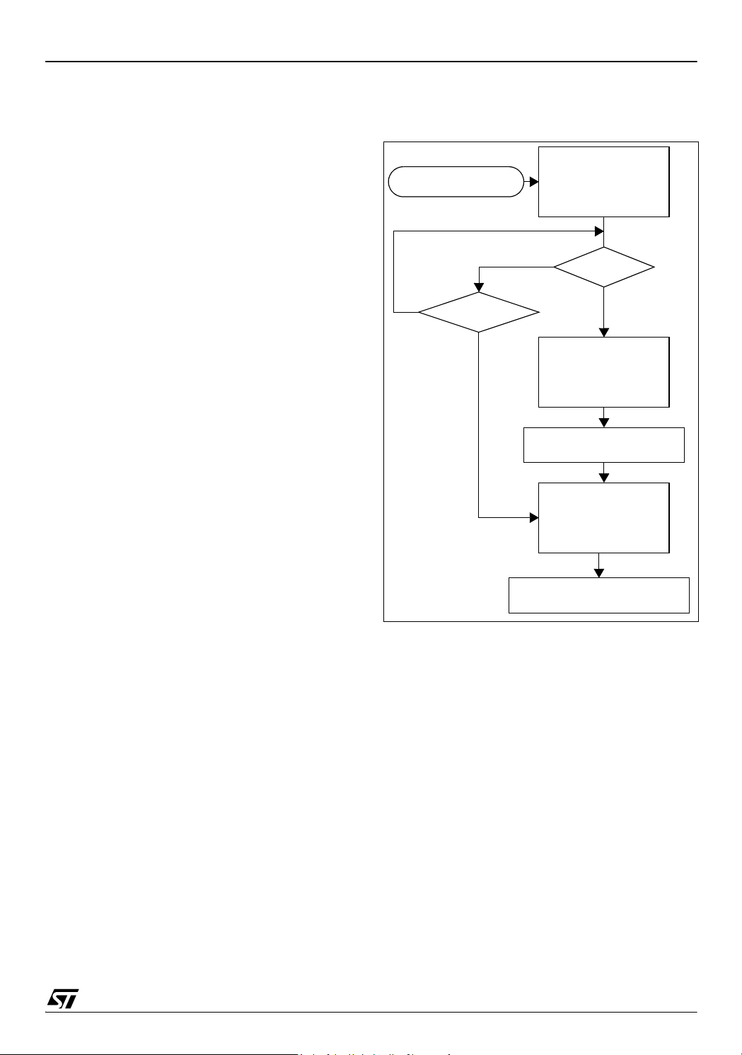
POWER SAVING MODES (Cont’d)
ST7LITE1
9.3 WAIT MODE
WAIT mode places the MCU in a low power consumption mode by stopping the CPU.
This power saving mode is selected by calling the
‘WFI’ instruction.
All peripherals remain active. During WAIT mode,
the I bit of the CC register is cleared, to enable all
interrupts. All other registers and memory remain
unchanged. The MCU remains in WAIT mode until
an interrupt or RESET occurs, whereupon the Program Counter branches to the starting address of
the interrupt or Reset service routine.
The MCU will remain in WAIT mode until a Reset
or an Interrupt occurs, causing it to wake up.
Refer to Figure 22.
Figure 22. WAIT Mode Flow-chart
OSCILLATOR
WFI INSTRUCTION
N
INTERRUPT
Y
PERIPHERALS
CPU
IBIT
N
RESET
Y
OSCILLATOR
PERIPHERALS
CPU
IBIT
256 OR 4096 CPU CLOCK
CYCLE DELAY
OSCILLATOR
PERIPHERALS
CPU
IBIT
ON
ON
OFF
0
ON
OFF
ON
0
ON
ON
ON
X
1)
FETCH RESET VECTOR
OR SERVICE INTERRUPT
Note:
1. Before servicing an interrupt, the CC register is
pushed on the stack. The I bit of the CC register is
set during the interrupt routine and cleared when
the CC register is popped.
39/131
1
Page 40

ST7LITE1
POWER SAVING MODES (Cont’d)
9.4 HALT MODE
The HALT mode is the lowest power consumption
mode of the MCU. It is entered by executing the
‘HALT’ instruction when ACTIVE-HALT is disabled
(see section 9.5 on page 41 for more details) and
when the AWUEN bit in the AWUCSR register is
cleared.
The MCU can exit HALT mode on reception of either a specific interrupt (see Table 5, “Interrupt
Mapping,” on page 35) or a RESET. When exiting
HALT mode by means of a RESET or an interrupt,
the oscillator is immediately turned on and the 256
or 4096 CPU cycle delay is used to stabilize the
oscillator. After the start up delay, the CPU
resumes operation by servicing the interrupt or by
fetching the reset vector which woke it up (see Fig-
ure 24).
When entering HALT mode, the I bit in the CC register is forced to 0 to enable interrupts. Therefore,
if an interrupt is pending, the MCU wakes up immediately.
In HALT mode, the main oscillator is turned off
causing all internal processing to be stopped, including the operation of the on-chip peripherals.
All peripherals are not clocked except the ones
which get their clock supply from another clock
generator (such as an external or auxiliary oscillator).
The compatibility of Watchdog operation with
HALT mode is configured by the “WDGHALT” option bit of the option byte. The HALT instruction
when executed while the Watchdog system is enabled, can generate a Watchdog RESET (see sec-
tion 15.1 on page 121 for more details).
Figure 23. HALT Timing Overview
Figure 24. HALT Mode Flow-chart
HALT INSTRUCTION
(Active Halt disabled)
(AWUCSR.AWUEN=0)
WATCHDOG
RESET
Y
CYCLE
WDGHALT
1
WATCHDOG
RESET
N
INTERRUPT
Y
1)
ENABLE
0
OSCILLATOR
PERIPHERALS
CPU
IBIT
N
3)
OSCILLATOR
PERIPHERALS
CPU
IBIT
256 OR 4096 CPU CLOCK
OSCILLATOR
PERIPHERALS
CPU
IBIT
FETCH RESET VECTOR
OR SERVICE INTERRUPT
DISABLE
2)
DELAY
OFF
OFF
OFF
0
ON
OFF
ON
X
5)
ON
ON
ON
X
4)
4)
HALTRUN RUN
HALT
INSTRUCTION
[Active Halt disabled]
40/131
1
256 OR 4096 CPU
CYCLE DELAY
RESET
OR
INTERRUPT
FETCH
VECTOR
Notes:
1. WDGHALT is an option bit. See option byte sec-
tion for more details.
2. Peripheral clocked with an external clock source
can still be active.
3. Only some specific interrupts can exit the MCU
from HALT mode (such as external interrupt). Refer to Table 5 Interrupt Mapping for more details.
4. Before servicing an interrupt, the CC register is
pushed on the stack. The I bit of the CC register is
set during the interrupt routine and cleared whenthe CC register is popped.
5. If the PLL is enabled by option byte, it outputs
the clock after a delay of t
STARTUP
(see Figure 11).
Page 41
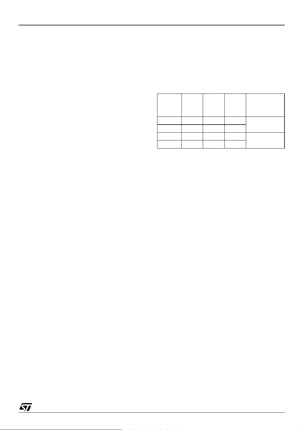
POWER SAVING MODES (Cont’d)
9.4.1 Halt Mode Recommendations
– Make sure that an external event is available to
wake up the microcontroller from Halt mode.
– When using an external interrupt to wake up the
microcontroller, reinitialize the corresponding I/O
as “Input Pull-up with Interrupt” before executing
the HALT instruction. The main reason for this is
that the I/O may be wrongly configured due to external interference or by an unforeseen logical
condition.
– For the same reason, reinitialize the level sensi-
tiveness of each external interrupt as a precautionary measure.
– The opcode for the HALT instruction is 0x8E. To
avoid an unexpected HALT instruction due to a
program counter failure, it is advised to clear all
occurrences of the data value 0x8E from memory. For example, avoid defining a constant in program memory with the value 0x8E.
– As the HALT instruction clears the interrupt mask
in the CC register to allow interrupts, the user
may choose to clear all pending interrupt bits before executing the HALT instruction. This avoids
entering other peripheral interrupt routines after
executing the external interrupt routine corresponding to the wake-up event (reset or external
interrupt).
ST7LITE1
9.5 ACTIVE-HALT MODE
ACTIVE-HALT mode is the lowest power consumption mode of the MCU with a real time clock
available. It is entered by executing the ‘HALT’ instruction. The decision to enter either in ACTIVEHALT or HALT mode is given by the LTCSR/ATCSR register status as shown in the following table:
LTCSR1
TB1IE bit
The MCU can exit ACTIVE-HALT mode on reception of a specific interrupt (see Table 5, “Interrupt
Mapping,” on page 35) or a RESET.
– When exiting ACTIVE-HALT mode by means of
a RESET, a 256 or 4096 CPU cycle delay occurs. After the start up delay, the CPU resumes
operation by fetching the reset vector which
woke it up (see Figure 26).
– When exiting ACTIVE-HALT mode by means of
an interrupt, the CPU immediately resumes operation by servicing the interrupt vector which woke
it up (see Figure 26).
When entering ACTIVE-HALT mode, the I bit in
the CC register is cleared to enable interrupts.
Therefore, if an interrupt is pending, the MCU
wakes up immediately (see Note 3).
In ACTIVE-HALT mode, only the main oscillator
and the selected timer counter (LT/AT) are running
to keep a wake-up time base. All other peripherals
are not clocked except those which get their clock
supply from another clock generator (such as external or auxiliary oscillator).
ATCSR
OVFIE
0xx0
00xx
1 xxx
x 101
bit
ATCSR
CK1 bit
ATCSR
CK0 bit
ACTIVE-HALT
mode disabled
ACTIVE-HALT
mode enabled
Meaning
Note: As soon as ACTIVE-HALT is enabled, exe-
cuting a HALT instruction while the Watchdog is
active does not generate a RESET.
This means that the device cannot spend more
than a defined delay in this power saving mode.
41/131
1
Page 42
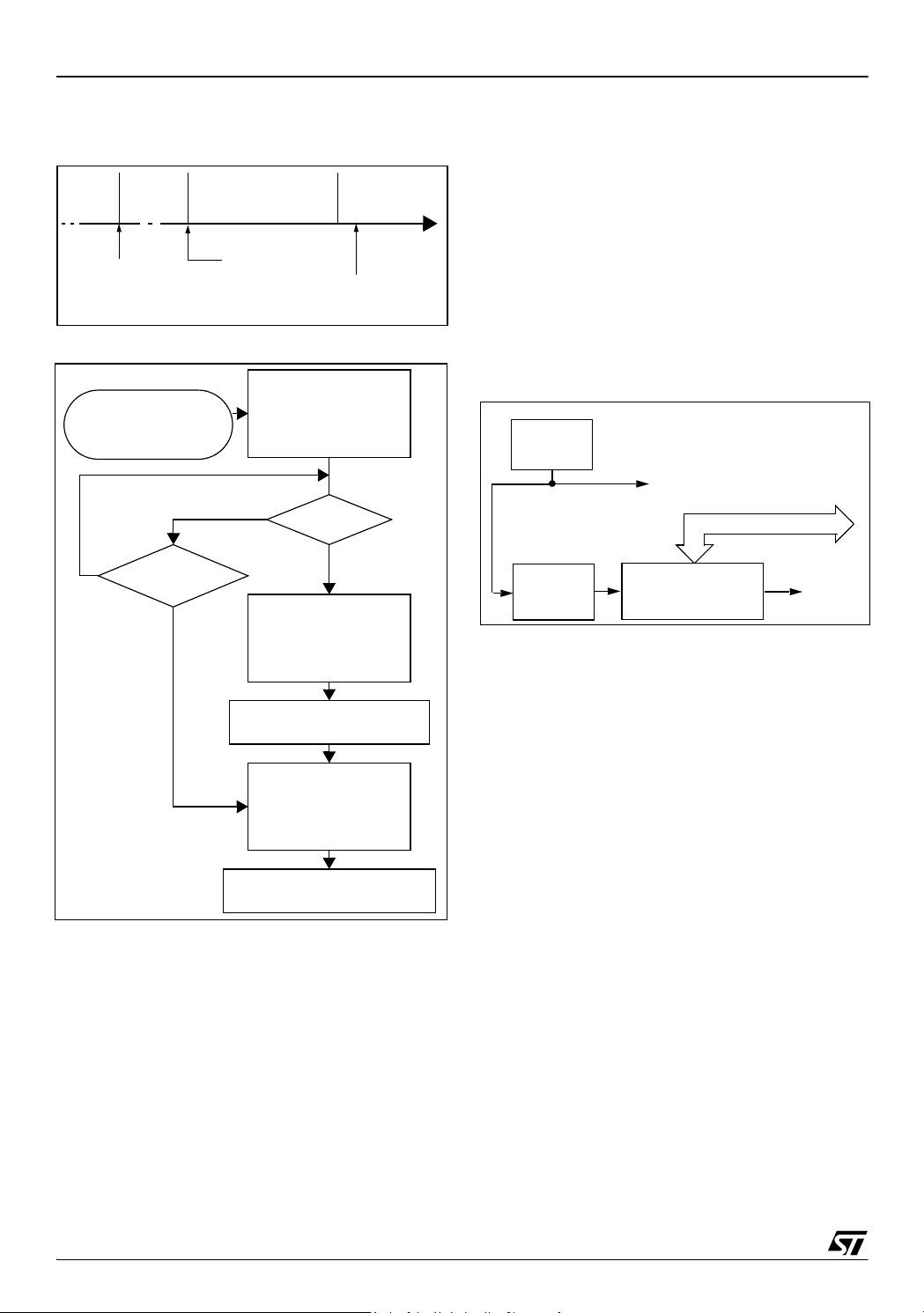
ST7LITE1
POWER SAVING MODES (Cont’d)
Figure 25. ACTIVE-HALT Timing Overview
ACTIVE
HALTRUN RUN
HALT
INSTRUCTION
[Active Halt Enabled]
256 OR 4096 CPU
CYCLE DELAY
RESET
OR
INTERRUPT
1)
FETCH
VECTOR
Figure 26. ACTIVE-HALT Mode Flow-chart
HALT INSTRUCTION
(Active Halt enabled)
(AWUCSR.AWUEN=0)
N
INTERRUPT
Y
OSCILLATOR
PERIPHERALS
CPU
IBIT
N
RESET
Y
3)
OSCILLATOR
PERIPHERALS
CPU
IBIT
256 OR 4096 CPU CLOCK
CYCLE
OSCILLATOR
PERIPHERALS
CPU
IBIT
FETCH RESET VECTOR
OR SERVICE INTERRUPT
2)
2)
DELAY
ON
OFF
OFF
0
ON
OFF
ON
X
ON
ON
ON
X
4)
4)
Notes:
1. This delay occurs only if the MCU exits ACTIVE-
HALT mode by means of a RESET.
2. Peripherals clocked with an external clock
source can still be active.
3. Only the RTC1 interrupt and some specific interrupts can exit the MCU from ACTIVE-HALT mode.
Refer to Table 5, “Interrupt Mapping,” on page 35
for more details.
4. Before servicing an interrupt, the CC register is
pushed on the stack. The I bit of the CC register is
set during the interrupt routine and cleared when
the CC register is popped.
9.6 AUTO WAKE UP FROM HALT MODE
Auto Wake Up From Halt (AWUFH) mode is similar to Halt mode with the addition of a specific internal RC oscillator for wake-up (Auto Wake Up
from Halt Oscillator). Compared to ACTIVE-HALT
mode, AWUFH has lower power consumption (the
main clock is not kept running, but there is no accurate realtime clock available.
It is entered by executing the HALT instruction
when the AWUEN bit in the AWUCSR register has
been set.
Figure 27. AWUFH Mode Block Diagram
AWU RC
oscillator
f
AWU_RC
to Timer input capture
AWUFH
/64
divider
AWUFH
prescaler/1 .. 255
interrupt
(ei0 source)
As soon as HALT mode is entered, and if the
AWUEN bit has been set in the AWUCSR register,
the AWU RC oscillator provides a clock signal
(f
AWU_RC
). Its frequency is divided by a fixed divider and a programmable prescaler controlled by the
AWUPR register. The output of this prescaler provides the delay time. When the delay has elapsed
the AWUF flag is set by hardware and an interrupt
wakes-up the MCU from Halt mode. At the same
time the main oscillator is immediately turned on
and a 256 or 4096 cycle delay is used to stabilize
it. After this start-up delay, the CPU resumes operation by servicing the AWUFH interrupt. The AWU
flag and its associated interrupt are cleared by
software reading the AWUCSR register.
To compensate for any frequency dispersion of
the AWU RC oscillator, it can be calibrated by
measuring the clock frequency f
AWU_RC
and then
calculating the right prescaler value. Measurement
mode is enabled by setting the AWUM bit in the
AWUCSR register in Run mode. This connects
f
AWU_RC
load timer, allowing the f
to the input capture of the 12-bit Auto-Re-
AWU_RC
to be measured
using the main oscillator clock as a reference timebase.
42/131
1
Page 43
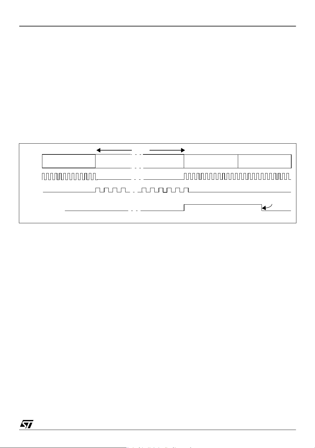
POWER SAVING MODES (Cont’d)
Similarities with Halt mode
The following AWUFH mode behaviour is the
same as normal Halt mode:
– The MCU can exit AWUFH mode by means of
any interrupt with exit from Halt capability or a reset (see Section 9.4 HALT MODE).
– When entering AWUFH mode, the I bit in the CC
register is forced to 0 to enable interrupts. Therefore, if an interrupt is pending, the MCU wakes
up immediately.
Figure 28. AWUF Halt Timing Diagram
t
AWU
ST7LITE1
– In AWUFH mode, the main oscillator is turned off
causing all internal processing to be stopped, including the operation of the on-chip peripherals.
None of the peripherals are clocked except those
which get their clock supply from another clock
generator (such as an external or auxiliary oscillator like the AWU oscillator).
– The compatibility of Watchdog operation with
AWUFH mode is configured by the WDGHALT
option bit in the option byte. Depending on this
setting, the HALT instruction when executed
while the Watchdog system is enabled, can generate a Watchdog RESET.
RUN MODE HALT MODE 256 OR 4096 t
f
CPU
f
AWU_RC
AWUFH interrupt
CPU
RUN MODE
Clear
by software
43/131
1
Page 44

ST7LITE1
POWER SAVING MODES (Cont’d)
Figure 29. AWUFH Mode Flow-chart Notes:
1. WDGHALT is an option bit. See option byte sec-
HALT INSTRUCTION
(Active-Halt disabled)
(AWUCSR.AWUEN=1)
ENABLE
WDGHALT
1
WATCHDOG
RESET
1)
WATCHDOG
0
AWU RC OSC ON
MAIN OSC
PERIPHERALS
CPU
I[1:0] BITS
DISABLE
2)
OFF
OFF
OFF
10
tion for more details.
2. Peripheral clocked with an external clock source
can still be active.
3. Only an AWUFH interrupt and some specific interrupts can exit the MCU from HALT mode (such
as external interrupt). Refer to Table 5, “Interrupt
Mapping,” on page 35 for more details.
4. Before servicing an interrupt, the CC register is
pushed on the stack. The I[1:0] bits of the CC register are set to the current software priority level of
the interrupt routine and recovered when the CC
register is popped.
5. If the PLL is enabled by option byte, it outputs
the clock after an additional delay of t
Figure 11).
STARTUP
(see
N
INTERRUPT
Y
N
3)
AWU RC OSC OFF
MAIN OSC
PERIPHERALS
CPU
I[1:0] BITS
256 OR 4096 CPU CLOCK
AWU RC OSC OFF
MAIN OSC
PERIPHERALS
CPU
I[1:0] BITS
FETCH RESET VECTOR
OR SERVICE INTERRUPT
RESET
Y
CYCLE
DELAY
ON
OFF
ON
XX
5)
ON
ON
ON
XX
4)
4)
44/131
1
Page 45

POWER SAVING MODES (Cont’d)
9.6.0.1 Register Description
70
AWUFH CONTROL/STATUS REGISTER
AWU
AWU
AWU
AWU
(AWUCSR)
Read/Write
PR7
PR6
PR5
PR4
AWU
PR3
Reset Value: 0000 0000 (00h)
Bits 7:0= AWUPR[7:0] Auto Wake Up Prescaler
70
00000
AWUFAWUMAWU
EN
Bits 7:3 = Reserved.
Bit 1= AWUF Auto Wake Up Flag
This bit is set by hardware when the AWU module
These 8 bits define the AWUPR Dividing factor (as
explained below:
AWUPR[7:0] Dividing factor
00h Forbidden
01h 1
... ...
FEh 254
FFh 255
generates an interrupt and cleared by software on
reading AWUCSR. Writing to this bit does not
change its value.
0: No AWU interrupt occurred
In AWU mode, the period that the MCU stays in
Halt Mode (t
in Figure 28 on page 43) is de-
AWU
fined by
1: AWU interrupt occurred
t
AWU
64 AW U PR×
--------------------------t
f
AWURC
Bit 1= AWUM Auto Wake Up Measurement
This bit enables the AWU RC oscillator and connects its output to the inputcapture of the 12-bit
Auto-Reload timer. This allows the timer to be
used to measure the AWU RC oscillator dispersion and then compensate this dispersion by providing the right value in the AWUPRE register.
0: Measurement disabled
1: Measurement enabled
This prescaler register can be programmed to
modify the time that the MCU stays in Halt mode
before waking up automatically.
Note: If 00h is written to AWUPR, depending on
the product, an interrupt is generated immediately
after a HALT instruction, or the AWUPR remains
inchanged.
1
AWU
PR2
+×=
ST7LITE1
AWU
PR1
RCSTRT
AWU
PR0
Bit 0 = AWUEN Auto Wake Up From Halt Enabled
This bit enables the Auto Wake Up From Halt feature: once HALT mode is entered, the AWUFH
wakes up the microcontroller after a time delay dependent on the AWU prescaler value. It is set and
cleared by software.
0: AWUFH (Auto Wake Up From Halt) mode disa-
bled
1: AWUFH (Auto Wake Up From Halt) mode ena-
bled
AWUFH PRESCALER REGISTER (AWUPR)
Read/Write
Table 7. AWU Register Map and Reset Values
Address
(Hex.)
0049h
004Ah
Register
Label
AWUPR
Reset Value
AWUCSR
Reset Value
76543210
AWUPR71AWUPR61AWUPR51AWUPR41AWUPR31AWUPR21AWUPR11AWUPR0
00000AWUFAWUMAWUEN
1
45/131
1
Page 46

ST7LITE1
10 I/O PORTS
10.1 INTRODUCTION
The I/O ports allow data transfer. An I/O port can
contain up to 8 pins. Each pin can be programmed
independently either as a digital input or digital
output. In addition, specific pins may have several
other functions. These functions can include external interrupt, alternate signal input/output for onchip peripherals or analog input.
10.2 FUNCTIONAL DESCRIPTION
A Data Register (DR) and a Data Direction Register (DDR) are always associated with each port.
The Option Register (OR), which allows input/output options, may or may not be implemented. The
following description takes into account the OR
register. Refer to the Port Configuration table for
device specific information.
An I/O pin is programmed using the corresponding
bits in the DDR, DR and OR registers: bit x corresponding to pin x of the port.
Figure 30 shows the generic I/O block diagram.
10.2.1 Input Modes
Clearing the DDRx bit selects input mode. In this
mode, reading its DR bit returns the digital value
from that I/O pin.
If an OR bit is available, different input modes can
be configured by software: floating or pull-up. Refer to I/O Port Implementation section for configuration.
Notes:
1. Writing to the DR modifies the latch value but
does not change the state of the input pin.
2. Do not use read/modify/write instructions
(BSET/BRES) to modify the DR register.
External Interrupt Function
Depending on the device, setting the ORx bit while
in input mode can configure an I/O as an input with
interrupt. In this configuration, a signal edge or level input on the I/O generates an interrupt request
via the corresponding interrupt vector (eix).
Falling or rising edge sensitivity is programmed independently for each interrupt vector. The External Interrupt Control Register (EICR) or the Miscellaneous Register controls this sensitivity, depending on the device.
External interrupts are hardware interrupts. Fetching the corresponding interrupt vector automatically clears the request latch. Modifying the sensitivity
bits will clear any pending interrupts.
10.2.2 Output Modes
Setting the DDRx bit selects output mode. Writing
to the DR bits applies a digital value to the I/O
through the latch. Reading the DR bits returns the
previously stored value.
If an OR bit is available, different output modes
can be selected by software: push-pull or opendrain. Refer to I/O Port Implementation section for
configuration.
DR Value and Output Pin Status
DR Push-Pull Open-Drain
0V
1VOHFloating
OL
V
OL
10.2.3 Alternate Functions
Many ST7s I/Os have one or more alternate functions. These may include output signals from, or
input signals to, on-chip peripherals. The Device
Pin Description table describes which peripheral
signals can be input/output to which ports.
A signal coming from an on-chip peripheral can be
output on an I/O. To do this, enable the on-chip
peripheral as an output (enable bit in the peripheral’s control register). The peripheral configures the
I/O as an output and takes priority over standard I/
O programming. The I/O’s state is readable by addressing the corresponding I/O data register.
Configuring an I/O as floating enables alternate
function input. It is not recommended to configure
an I/O as pull-up as this will increase current consumption. Before using an I/O as an alternate input, configure it without interrupt. Otherwise spurious interrupts can occur.
Configure an I/O as input floating for an on-chip
peripheral signal which can be input and output.
Caution:
I/Os which can be configured as both an analog
and digital alternate function need special attention. The user must control the peripherals so that
the signals do not arrive at the same time on the
same pin. If an external clock is used, only the
clock alternate function should be employed on
that I/O pin and not the other alternate function.
46/131
1
Page 47
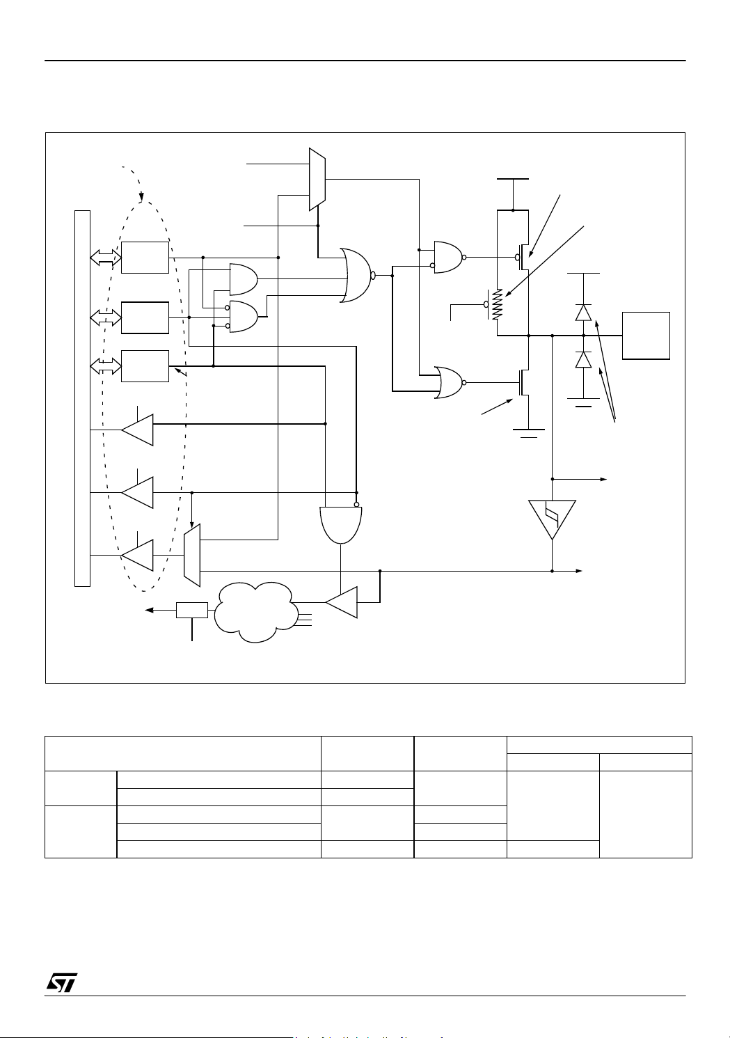
I/O PORTS (Cont’d)
Figure 30. I/O Port General Block Diagram
ST7LITE1
REGISTER
ACCESS
DATA BUS
DDR SEL
DR
DDR
OR
OR SEL
DR SEL
ALTERNATE
OUTPUT
From on-chip peripheral
ALTERNATE
ENABLE
BIT
If implemented
1
1
0
PULL-UP
CONDITION
N-BUFFER
V
DD
CMOS
SCHMITT
TRIGGER
P-BUFFER
(see table below)
PULL-UP
(see table below)
V
DD
PAD
DIODES
(see table below)
ANALOG
INPUT
0
EXTERNAL
INTERRUPT
REQUEST (eix)
SENSITIVITY
SELECTION
Combinational
Table 8. I/O Port Mode Options
Configuration Mode Pull-Up P-Buffer
Input
Output
Floating with/without Interrupt Off
Pull-up with/without Interrupt On
Push-pull
Open Drain (logic level) Off
True Open Drain NI NI NI (see note)
Legend: NI - not implemented
Off - implemented not activated
On - implemented and activated
Logic
FROM
OTHER
BITS
Note: Refer to the Port Configuration
table for device specific information.
Off
Note: The diode to V
true open drain pads. A local protection between
the pad and V
vice against positive stress.
ALTERNATE
To on-chip peripheral
Diodes
to V
DD
Off
On
is implemented to protect the de-
OL
On
is not implemented in the
DD
INPUT
to V
SS
On
47/131
1
Page 48
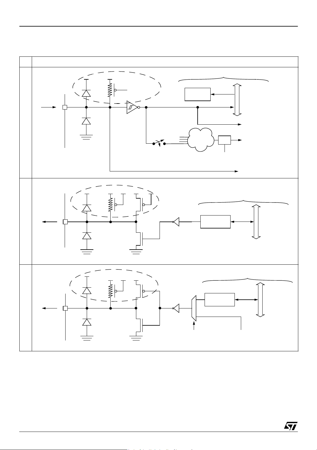
ST7LITE1
I/O PORTS (Cont’d)
Table 9. I/O Configurations
Hardware Configuration
1)
INPUT
2)
PAD
PAD
V
DD
R
V
DD
R
PU
PU
NOTE 3
NOTE 3
PULL-UP
CONDITION
INTERRUPT
CONDITION
FROM
OTHER
PINS
COMBINATIONAL
DR REGISTER ACCESS
DR
REGISTER
LOGIC
DR
REGISTER
W
R
POLARITY
SELECTION
DR REGISTER ACCESS
DATA B U S
ALTERNATE INPUT
To on-chip peripheral
EXTERNAL INTERRUPT
SOURCE (eix)
ANALOG INPUT
R/W
DATA BUS
OPEN-DRAIN OUTPUT
DR REGISTER ACCESS
DR
REGISTER
ALTERNATEALTERNATE
R/W
DATA B U S
2)
PUSH-PULL OUTPUT
PAD
NOTE 3
V
DD
R
PU
ENABLE OUTPUT
BIT From on-chip peripheral
Notes:
1. When the I/O port is in input configuration and the associated alternate function is enabled as an output,
reading the DR register will read the alternate function output status.
2. When the I/O port is in output configuration and the associated alternate function is enabled as an input,
the alternate function reads the pin status given by the DR register content.
3. For true open drain, these elements are not implemented.
48/131
1
Page 49

I/O PORTS (Cont’d)
Analog alternate function
Configure the I/O as floating input to use an ADC
input. The analog multiplexer (controlled by the
ADC registers) switches the analog voltage
present on the selected pin to the common analog
rail, connected to the ADC input.
Analog Recommendations
Do not change the voltage level or loading on any
I/O while conversion is in progress. Do not have
clocking pins located close to a selected analog
pin.
WARNING: The analog input voltage level must
be within the limits stated in the absolute maximum ratings.
ST7LITE1
Figure 31. Interrupt I/O Port State Transitions
01
INPUT
floating/pull-up
interrupt
10.4 UNUSED I/O PINS
Unused I/O pins must be connected to fixed voltage levels. Refer to Section 13.8.
00
INPUT
floating
(reset state)
10
OUTPUT
open-drain
XX
11
OUTPUT
push-pull
= DDR, OR
10.3 I/O PORT IMPLEMENTATION
The hardware implementation on each I/O port depends on the settings in the DDR and OR registers
and specific I/O port features such as ADC input or
open drain.
Switching these I/O ports from one state to another should be done in a sequence that prevents unwanted side effects. Recommended safe transitions are illustrated in Figure 31. Other transitions
are potentially risky and should be avoided, since
they may present unwanted side-effects such as
spurious interrupt generation.
10.5 LOW POWER MODES
Mode Description
WAIT
HALT
No effect on I/O ports. External interrupts
cause the device to exit from WAIT mode.
No effect on I/O ports. External interrupts
cause the device to exit from HALT mode.
10.6 INTERRUPTS
The external interrupt event generates an interrupt
if the corresponding configuration is selected with
DDR and OR registers and if the I bit in the CC
register is cleared (RIM instruction).
Interrupt Event
External interrupt on
selected external
event
Event
Flag
-
Enable
Control
Bit
DDRx
ORx
Exit
from
Wait
Yes Yes
Exit
from
Halt
49/131
1
Page 50

ST7LITE1
I/O PORTS (Cont’d)
10.7 DEVICE-SPECIFIC I/O PORT CONFIGURATION
The I/O port register configurations are summarised as follows.
Standard Ports
PA7:0, PB6:0
MODE DDR OR
floating input 0 0
pull-up input 0 1
open drain output 1 0
push-pull output 1 1
Interrupt Ports
Ports where the external interrupt capability is
selected using the EISR register
MODE DDR OR
floating input 0 0
pull-up interrupt input 0 1
open drain output 1 0
push-pull output 1 1
Table 10. Port Configuration (Standard ports)
Port Pin name
Port A PA7:0 floating
Port B PB6:0 floating pull-up open drain push-pull
OR = 0 OR = 1 OR = 0 OR = 1
Input Output
pull-up
open drain push-pull
Note: On ports where the external interrupt capability is selected using the EISR register, the configuration will be as follows:
Port Pin name
Port A PA7:0 floating
Port B PB6:0 floating pull-up interrupt open drain push-pull
OR = 0 OR = 1 OR = 0 OR = 1
Input Output
pull-up interrupt
open drain push-pull
Table 11. I/O Port Register Map and Reset Values
Address
(Hex.)
0000h
0001h
0002h
0003h
0004h
0005h
50/131
Register
Label
PADR
Reset Value
PADDR
Reset Value
PAOR
Reset Value
PBDR
Reset Value
PBDDR
Reset Value
PBOR
Reset Value
76543210
MSB
1111111
MSB
0000000
MSB
0100000
MSB
1111111
MSB
0000000
MSB
0000000
LSB
1
LSB
0
LSB
0
LSB
1
LSB
0
LSB
0
1
Page 51

11 ON-CHIP PERIPHERALS
11.1 WATCHDOG TIMER (WDG)
ST7LITE1
11.1.1 Introduction
The Watchdog timer is used to detect the occurrence of a software fault, usually generated by external interference or by unforeseen logical conditions, which causes the application program to
abandon its normal sequence. The Watchdog circuit generates an MCU reset on expiry of a programmed time period, unless the program refreshes the counter’s contents before the T6 bit becomes cleared.
11.1.2 Main Features
■ Programmable free-running downcounter (64
increments of 16000 CPU cycles)
■ Programmable reset
■ Reset (if watchdog activated) when the T6 bit
reaches zero
Figure 32. Watchdog Block Diagram
RESET
■ Optional reset on HALT instruction
(configurable by option byte)
■ Hardware Watchdog selectable by option byte
11.1.3 Functional Description
The counter value stored in the CR register (bits
T[6:0]), is decremented every 16000 machine cycles, and the length of the timeout period can be
programmed by the user in 64 increments.
If the watchdog is activated (the WDGA bit is set)
and when the 7-bit timer (bits T[6:0]) rolls over
from 40h to 3Fh (T6 becomes cleared), it initiates
a reset cycle pulling low the reset pin for typically
30µs.
f
CPU
WATCHDOG CONTROL REGISTER (CR)
T5
WDGA
T6
T4
7-BIT DOWNCOUNTER
CLOCK DIVIDER
÷16000
T3
T2
T1
T0
51/131
1
Page 52

ST7LITE1
WATCHDOG TIMER (Cont’d)
The application program must write in the CR register at regular intervals during normal operation to
prevent an MCU reset. This downcounter is freerunning: it counts down even if the watchdog is
disabled. The value to be stored in the CR register
must be between FFh and C0h (see Table 12
.Watchdog Timing):
– The WDGA bit is set (watchdog enabled)
– The T6 bit is set to prevent generating an imme-
diate reset
– The T[5:0] bits contain the number of increments
which represents the time delay before the
watchdog produces a reset.
Following a reset, the watchdog is disabled. Once
activated it cannot be disabled, except by a reset.
The T6 bit can be used to generate a software reset (the WDGA bit is set and the T6 bit is cleared).
If the watchdog is activated, the HALT instruction
will generate a Reset.
Table 12.Watchdog Timing
f
= 8MHz
CPU
WDG
Counter
Code
C0h 1 2
FFh 127 128
min
[ms]
max
[ms]
Notes:
1. The timing variation shown in Table 12 is due to
the unknown status of the prescaler when writing
to the CR register.
2. The number of CPU clock cycles applied during
the RESET phase (256 or 4096) must be taken
into account in addition to these timings.
11.1.4 Hardware Watchdog Option
If Hardware Watchdog is selected by option byte,
the watchdog is always active and the WDGA bit in
the CR is not used.
Refer to the Option Byte description in section 15
on page 121.
11.1.4.1 Using Halt Mode with the WDG (WDGHALT option)
If Halt mode with Watchdog is enabled by option
byte (No watchdog reset on HALT instruction), it is
recommended before executing the HALT instruction to refresh the WDG counter, to avoid an unexpected WDG reset immediately after waking up
the microcontroller. Same behavior in active-halt
mode.
52/131
1
Page 53

WATCHDOG TIMER (Cont’d)
ST7LITE1
11.1.5 Interrupts
None.
Bit 6:0 = T[6:0] 7-bit timer (MSB to LSB).
These bits contain the decremented value. A reset
is produced when it rolls over from 40h to 3Fh (T6
becomes cleared).
11.1.6 Register Description
CONTROL REGISTER (CR)
Read/Write
Reset Value: 0111 1111 (7Fh)
70
WDGA T6 T5 T4 T3 T2 T1 T0
Bit 7 = WDGA Activation bit.
This bit is set by software and only cleared by
hardware after a reset. When WDGA = 1, the
watchdog can generate a reset.
0: Watchdog disabled
1: Watchdog enabled
Note: This bit is not used if the hardware watchdog option is enabled by option byte.
53/131
1
Page 54

ST7LITE1
WATCHDOG TIMER (Cont’d)
Table 13. Watchdog Timer Register Map and Reset Values
Address
(Hex.)
002Eh
Register
Label
WDGCR
Reset Value
76543210
WDGA
0
T6
T5
1
1
T4
1
T3
T2
1
1
T1
T0
1
1
54/131
1
Page 55

11.2 12-BIT AUTORELOAD TIMER 2 (AT2)
ST7LITE1
11.2.1 Introduction
The 12-bit Autoreload Timer can be used for general-purpose timing functions. It is based on a freerunning 12-bit upcounter with an input capture register and four PWM output channels. There are 6
external pins:
– Four PWM outputs
– ATIC pin for the Input Capture function
– BREAK pin for forcing a break condition on the
PWM outputs
11.2.2 Main Features
■ 12-bit upcounter with 12-bit autoreload register
(ATR)
Figure 33. Block Diagram
ATIC
f
LTIMER
(1 ms
timebase
@ 8MHz)
f
CPU
32 MHz
ATICR
ATCSR
12-BIT INPUT CAPTURE REGISTER
IC INTERRUPT
REQUEST
f
COUNTER
CNTR
ATR
■ Maskable overflow interrupt
■ Generation of four independent PWMx signals
■ Frequency 2KHz-4MHz (@ 8 MHz f
CPU
– Programmable duty-cycles
– Polarity control
– Programmable output modes
– Maskable Compare interrupt
■ Input Capture
– 12-bit input capture register (ATICR)
– Triggered by rising and falling edges
– Maskable IC interrupt
OVF INTERRUPT
REQUEST
CMPIEOVFIEOVFCK0CK1ICIEICF0
CMPF0
CMPF1
CMPF2
CMPF3
12-BIT UPCOUNTER
12-BIT AUTORELOAD REGISTER
CMP
INTERRUPT
REQUEST
)
DCR0H
Preload
DCR0L
Preload
on OVF Event
IF TRAN=1
12-BIT DUTY CYCLE VALUE (shadow)
4 PWM Channels
CMPFx bit
COMP-
PARE
PWM GENERATION
f
PWM
OPx bit
POLARITY
OEx bit
PWMx
OUTPUT CONTROL
55/131
1
Page 56

ST7LITE1
12-BIT AUTORELOAD TIMER (Cont’d)
11.2.3 Functional Description
PWM Mode
This mode allows up to four Pulse Width Modulated signals to be generated on the PWMx output
pins. The PWMx output signals can be enabled or
disabled using the OEx bits in the PWMCR register.
PWM Frequency and Duty Cycle
The four PWM signals have the same frequency
) which is controlled by the counter period
(f
PWM
and the ATR register value.
= f
f
PWM
COUNTER
Following the above formula,
– If f
COUNTER
is 8 MHz (ATR register value = 4092), the
f
PWM
is 32 MHz, the maximum value of
minimum value is 8 KHz (ATR register value = 0)
– If f
COUNTER
is 4 Mhz, the maximum value of f
is 2 MHz (ATR register value = 4094),the minimum value is 1 KHz (ATR register value = 0).
Note: The maximum value of ATR is 4094 because it must be lower than the DCR value which
must be 4095 in this case.
At reset, the counter starts counting from 0.
When a upcounter overflow occurs (OVF event),
the preloaded Duty cycle values are transferred to
the Duty Cycle registers and the PWMx signals
are set to a high level. When the upcounter matches the DCRx value the PWMx signals are set to a
low level. To obtain a signal on a PWMx pin, the
/ (4096 - ATR)
PWM
contents of the corresponding DCRx register must
be greater than the contents of the ATR register.
The polarity bits can be used to invert any of the
four output signals. The inversion is synchronized
with the counter overflow if the TRAN bit in the
TRANCR register is set (reset value). See Figure
34.
Figure 34. PWM Inversion Diagram
inverter
PWMx
PWMxCSR Register
OPx
TRANCR Register
TRAN
counter
overflow
DFF
The maximum available resolution for the PWMx
duty cycle is:
Resolution = 1 / (4096 - ATR)
Note: To get the maximum resolution (1/4096), the
ATR register must be 0. With this maximum resolution, 0% and 100% can be obtained by changing
the polarity.
PWMx
PIN
Figure 35. PWM Function
4095
DUTY CYCLE
REGISTER
(DCRx)
AUTO-RELOAD
COUNTER
REGISTER
(ATR)
000
WITH OE=1
AND OPx=0
WITH OE=1
AND OPx=1
PWMx OUTPUT
56/131
1
t
Page 57

12-BIT AUTORELOAD TIMER (Cont’d)
Figure 36. PWM Signal from 0% to 100% Duty Cycle
f
COUNTER
ATR= FFDh
ST7LITE1
PWMx OUTPUTtWITH OEx=1
PWMx OUTPUT
WITH OEx=1
AND OPx=0
AND OPx=1
COUNTER
DCRx=000h
DCRx=FFDh
DCRx=FFEh
DCRx=000h
FFDh FFEh FFFh FFDh FFEh FFFh FFDh FFEh
Output Compare Mode
To use this function, load a 12-bit value in the
DCRxH and DCRxL registers.
When the 12-bit upcounter (CNTR) reaches the
value stored in the DCRxH and DCRxL registers,
the CMPF bit in the PWMxCSR register is set and
an interrupt request is generated if the CMPIE bit
is set.
Note: The output compare function is only available for DCRx values other than 0 (reset value).
Break Function
The break function is used to perform an emergency shutdown of the power converter.
The break function is activated by the external
BREAK pin (active low). In order to use the
BREAK pin it must be previously enabled by software setting the BPEN bit in the BREAKCR register.
When a low level is detected on the BREAK pin,
the BA bit is set and the break function is activated.
Software can set the BA bit to activate the break
function without using the BREAK pin.
When the break function is activated (BA bit =1):
– The break pattern (PWM[3:0] bits in the BREAK-
CR) is forced directly on the PWMx output pins
(after the inverter).
– The 12-bit PWM counter is set to its reset value.
– The ARR, DCRx and the corresponding shadow
registers are set to their reset values.
– The PWMCR register is reset.
When the break function is deactivated after ap-
plying the break (BA bit goes from 1 to 0 by software):
– The control of PWM outputs is transferred to the
port registers.
57/131
1
Page 58
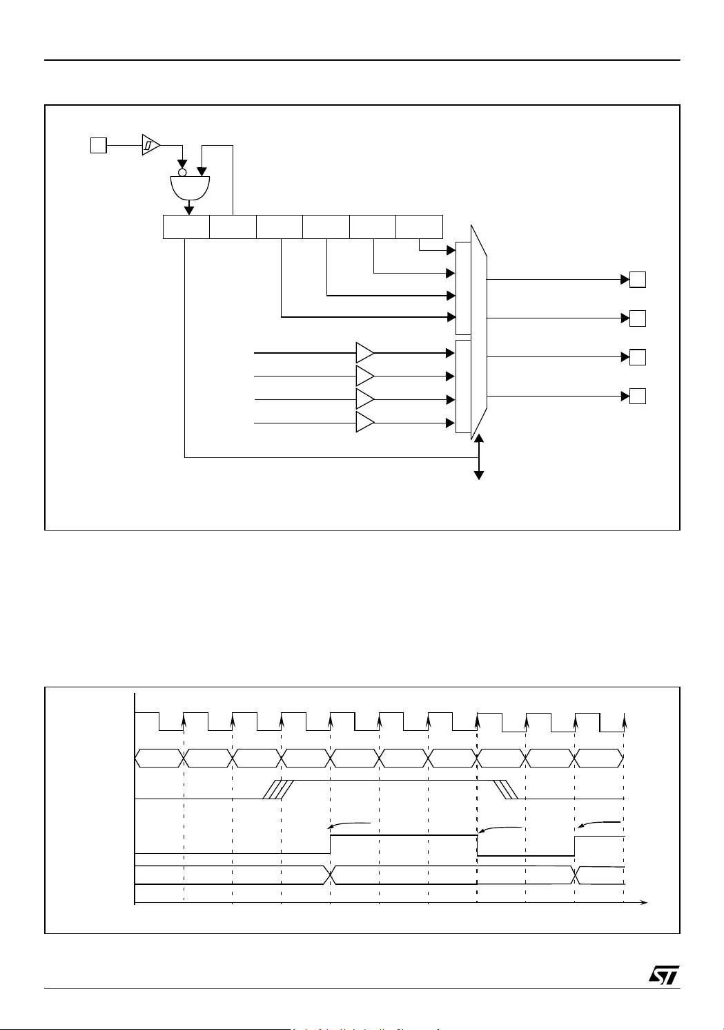
ST7LITE1
Figure 37. Block Diagram of Break Function
BREAK pin
(Active Low)
BREAKCR Register
PWM0
PWM1
PWM2
PWM3
Note:
The BREAK pin value is latched by the BA bit.
(Inverters)
PWM0PWM1PWM2PWM3BPENBA
1
PWM0
PWM1
PWM2
PWM3
0
When BA is set:
PWM counter -> Reset value
ARR & DCRx -> Reset value
PWM Mode -> Reset value
11.2.3.1 Input Capture
The 12-bit ATICR register is used to latch the value of the 12-bit free running upcounter after a rising or falling edge is detected on the ATIC pin.
When an input capture occurs, the ICF bit is set
and the ATICR register contains the value of the
Figure 38. Input Capture Timing Diagram
f
COUNTER
COUNTER
ATIC PIN
ICF FLAG
ICR REGISTER
01h
02h 03h 04h 05h 06h 07h
xxh
free running upcounter. An IC interrupt is generated if the ICIE bit is set. The ICF bit is reset by reading the ATICR register when the ICF bit is set. The
ATICR is a read only register and always contains
the free running upcounter value which corresponds to the most recent input capture. Any further input capture is inhibited while the ICF bit is
set.
08h 09h 0Ah
INTERRUPT
ATICR READ
04h
INTERRUPT
09h
t
58/131
1
Page 59
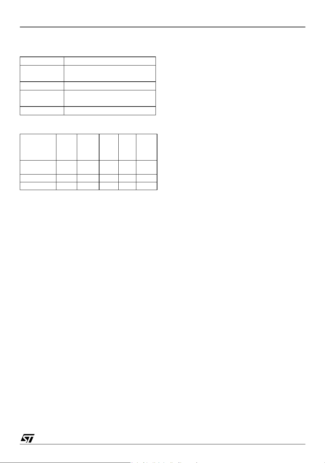
12-BIT AUTORELOAD TIMER (Cont’d)
11.2.4 Low Power Modes
Mode Description
SLOW
The input frequency is divided
by 32
WAIT No effect on AT timer
ACTIVE-HALT
AT timer halted except if CK0=1,
CK1=0 and OVFIE=1
HALT AT timer halted
11.2.5 Interrupts
ST7LITE1
The OVF event is mapped on a separate vector
(see Interrupts chapter).
They generate an interrupt if the enable bit is set in
the ATCSR register and the interrupt mask in the
CC register is reset (RIM instruction).
Note 2: Only if CK0=1 and CK1=0 (f
f
)
LTIMER
COUNTER
=
Exit
Interrupt
Event
Overflow
Event
IC Event ICF ICIE Yes No No
CMP Event CMPF0 CMPIE Yes No No
Event
1)
Enable
Control
Flag
OVF OVIE Yes No Yes
Bit
Exit
from
Wait
from
Halt
Exit
from
Active-
Halt
2)
Note 1: The CMP and IC events are connected to
the same interrupt vector.
59/131
1
Page 60
ST7LITE1
12-BIT AUTORELOAD TIMER (Cont’d)
11.2.6 Register Description
TIMER CONTROL STATUS REGISTER
(ATCSR)
Read / Write
Reset Value: 0x00 0000 (x0h)
76 0
Bit 2 = OVF Overflow Flag.
This bit is set by hardware and cleared by software
by reading the TCSR register. It indicates the transition of the counter from FFFh to ATR value.
0: No counter overflow occurred
1: Counter overflow occurred
0 ICF ICIE CK1 CK0 OVF OVFIE CMPIE
Bit 7 = Reserved.
Bit 6 = ICF Input Capture Flag.
This bit is set by hardware and cleared by software
by reading the ATICR register (a read access to
ATICRH or ATICRL will clear this flag). Writing to
this bit does not change the bit value.
0: No input capture
1: An input capture has occurred
Bit 5 = ICIE IC Interrupt Enable.
This bit is set and cleared by software.
0: Input capture interrupt disabled
1: Input capture interrupt enabled
Bits 4:3 = CK[1:0] Counter Clock Selection.
These bits are set and cleared by software and
cleared by hardware after a reset. They select the
clock frequency of the counter.
Counter Clock Selection CK1 CK0
OFF 0 0
(1 ms timebase @ 8 MHz)
f
LTIMER
f
CPU
32 MHz
2)
1)
01
10
11
Bit 1 = OVFIE Overflow Interrupt Enable.
This bit is read/write by software and cleared by
hardware after a reset.
0: OVF interrupt disabled.
1: OVF interrupt enabled.
Bit 0 = CMPIE Compare Interrupt Enable.
This bit is read/write by software and cleared by
hardware after a reset. It can be used to mask the
interrupt generated when the CMPF bit is set.
0: CMPF interrupt disabled.
1: CMPF interrupt enabled.
COUNTER REGISTER HIGH (CNTRH)
Read only
Reset Value: 0000 0000 (000h)
15 8
0000
CNTR11CNTR
10
CNTR9 CNTR8
COUNTER REGISTER LOW (CNTRL)
Read only
Reset Value: 0000 0000 (000h)
70
CNTR7 CNTR6 CNTR5 CNTR4 CNTR3 CNTR2 CNTR1 CNTR0
Note 1: PWM mode and Output Compare modes
are not available at this frequency.
Note 2: ATICR counter may return inaccurate results when read. It is therefore not recommended
to use Input Capture mode at this frequency.
60/131
1
Bits 15:12 = Reserved.
Bits 11:0 = CNTR[11:0] Counter Value.
This 12-bit register is read by software and cleared
by hardware after a reset. The counter is incremented continuously as soon as a counter clok is
selected. To obtain the 12-bit value, software
should read the counter value in two consecutive
read operations, LSB first. When a counter overflow occurs, the counter restarts from the value
specified in the ATR register.
Page 61

12-BIT AUTORELOAD TIMER (Cont’d)
ST7LITE1
AUTORELOAD REGISTER (ATRH)
Read / Write
Reset Value: 0000 0000 (00h)
PWMx CONTROL STATUS REGISTER
(PWMxCSR)
Read / Write
Reset Value: 0000 0000 (00h)
15 8
76 0
0 0 0 0 ATR11 ATR10 ATR9 ATR8
000000OPxCMPFx
AUTORELOAD REGISTER (ATRL)
Read / Write
Bits 7:2= Reserved, must be kept cleared.
Reset Value: 0000 0000 (00h)
70
Bit 1 = OPx PWMx Output Polarity.
This bit is read/write by software and cleared by
ATR7 ATR6 ATR5 ATR4 ATR3 ATR2 ATR1 ATR0
hardware after a reset. This bit selects the polarity
of the PWM signal.
0: The PWM signal is not inverted.
Bits 11:0 = ATR[11:0] Autoreload Register.
1: The PWM signal is inverted.
This is a 12-bit register which is written by software. The ATR register value is automatically
loaded into the upcounter when an overflow occurs. The register value is used to set the PWM
frequency.
Bit 0 = CMPFx PWMx Compare Flag.
This bit is set by hardware and cleared by software
by reading the PWMxCSR register. It indicates
that the upcounter value matches the DCRx register value.
PWM OUTPUT CONTROL REGISTER
(PWMCR)
0: Upcounter value does not match DCR value.
1: Upcounter value matches DCR value.
Read/Write
Reset Value: 0000 0000 (00h)
BREAK CONTROL REGISTER (BREAKCR)
70
Read/Write
Reset Value: 0000 0000 (00h)
0OE30OE20OE10OE0
70
Bits 7:0 = OE[3:0] PWMx output enable.
These bits are set and cleared by software and
cleared by hardware after a reset.
0: PWM mode disabled. PWMx Output Alternate
Function disabled (I/O pin free for general purpose I/O)
1: PWM mode enabled
0 0 BA BPEN PWM3 PWM2 PWM1 PWM0
Bits 7:6 = Reserved. Forced by hardware to 0.
Bit 5 = BA Break Active.
This bit is read/write by software, cleared by hardware after reset and set by hardware when the
BREAK pin is low. It activates/deactivates the
Break function.
0: Break not active
1: Break active
61/131
1
Page 62
ST7LITE1
12-BIT AUTORELOAD TIMER (Cont’d)
Bit 4 = BPEN Break Pin Enable.
This bit is read/write by software and cleared by
hardware after Reset.
0: Break pin disabled
1: Break pin enabled
INPUT CAPTURE REGISTER HIGH (ATICRH)
Read only
Reset Value: 0000 0000 (00h)
15 8
Bit 3:0 = PWM[3:0] Break Pattern.
0 0 0 0 ICR11 ICR10 ICR9 ICR8
These bits are read/write by software and cleared
by hardware after a reset. They are used to force
the four PWMx output signals into a stable state
when the Break function is active.
INPUT CAPTURE REGISTER LOW (ATICRL)
Read only
Reset Value: 0000 0000 (00h)
PWMx DUTY CYCLE REGISTER HIGH (DCRxH)
70
Read / Write
Reset Value: 0000 0000 (00h)
15 8
ICR7 ICR6 ICR5 ICR4 ICR3 ICR2 ICR1 ICR0
Bits 15:12 = Reserved.
0 0 0 0 DCR11 DCR10 DCR9 DCR8
Bits 11:0 = ICR[11:0] Input Capture Data.
This is a 12-bit register which is readable by software and cleared by hardware after a reset. The
ATICR register contains captured the value of the
PWMx DUTY CYCLE REGISTER LOW (DCRxL)
Read / Write
Reset Value: 0000 0000 (00h)
70
12-bit CNTR register when a rising or falling edge
occurs on the ATIC pin. Capture will only be performed when the ICF flag is cleared.
TRANSFER CONTROL REGISTER (TRANCR)
Read/Write
DCR7 DCR6 DCR5 DCR4 DCR3 DCR2 DCR1 DCR0
Reset Value: 0000 0001 (01h)
Bits 15:12 = Reserved.
Bits 11:0 = DCR[11:0] PWMx Duty Cycle Value
This 12-bit value is written by software. It definesthe duty cycle of the corresponding PWM output
signal (see Figure 35).
In PWM mode (OEx=1 in the PWMCR register)
the DCR[11:0] bits define the duty cycle of the
PWMx output signal (see Figure 35). In Output
Compare mode, they define the value to be compared with the 12-bit upcounter value.
62/131
1
70
0000000TRAN
Bits 7:1 Reserved. Forced by hardware to 0.
Bit 0 = TRAN Transfer enable
This bit is read/write by software, cleared by hardware after each completed transfer and set by
hardware after reset.
It allows the value of the DCRx registers to be
transferred to the DCRx shadow registers after the
next overflow event.
The OPx bits are transferred to the shadow OPx
bits in the same way.
Page 63

12-BIT AUTORELOAD TIMER (Cont’d)
Table 14. Register Map and Reset Values
ST7LITE1
Address
(Hex.)
0D
0E
0F
10
11
12
13
14
15
16
17
18
19
1A
1B
1C
1D
1E
1F
20
Register
Label
ATCSR
Reset Value
CNTRH
Reset Value
CNTRL
Reset Value
ATRH
Reset Value
ATRL
Reset Value
PWMCR
Reset Value
PWM0CSR
Reset Value
PWM1CSR
Reset Value
PWM2CSR
Reset Value
PWM3CSR
Reset Value
DCR0H
Reset Value
DCR0L
Reset Value
DCR1H
Reset Value
DCR1L
Reset Value
DCR2H
Reset Value
DCR2L
Reset Value
DCR3H
Reset Value
DCR3L
Reset Value
ATICRH
Reset Value
ATICRL
Reset Value
76543210
0
0000
CNTR70CNTR80CNTR70CNTR60CNTR30CNTR20CNTR10CNTR0
0000
ATR7
0
0
000000
000000
000000
000000
0000
DCR70DCR6
0000
DCR70DCR6
0000
DCR70DCR6
0000
DCR70DCR6
0000
ICR7
0
ICF
0
ATR6
0
OE3
0
0
0
0
0
ICR6
0
ICIE
0
ATR5
0
0
DCR5
0
DCR5
0
DCR5
0
DCR5
0
ICR5
0
CK1
0
ATR4
0
OE2
0
DCR40DCR3
DCR40DCR3
DCR40DCR3
DCR40DCR3
ICR4
0
CK0
0
CNTR110CNTR100CNTR90CNTR8
ATR110ATR100ATR9
ATR3
0
0
DCR110DCR100DCR90DCR8
0
DCR110DCR100DCR90DCR8
0
DCR110DCR10
0
DCR110DCR100DCR90DCR8
0
ICR110ICR10
ICR3
0
OVF
0
ATR2
0
OE1
0
DCR2
0
DCR2
0
0
DCR2
0
DCR2
0
0
ICR2
0
OVFIE0CMPIE
0
0
0
ATR8
0
ATR1
0
0
OP0
0
OP1
0
OP2
0
OP3
0
DCR10DCR0
DCR10DCR0
DCR90DCR8
DCR10DCR0
DCR10DCR0
ICR9
0
ICR1
0
0
ATR0
0
OE0
0
CMPF0
0
CMPF1
0
CMPF2
0
CMPF3
0
0
0
0
0
0
0
0
0
ICR8
0
ICR0
0
63/131
1
Page 64

ST7LITE1
Address
(Hex.)
21
22
Register
Label
TRANCR
Reset Value
BREAKCR
Reset Value
76543210
0000000
00
BA
0
BPEN0PWM30PWM20PWM10PWM0
TRAN
1
0
64/131
1
Page 65

11.3 LITE TIMER 2 (LT2)
ST7LITE1
11.3.1 Introduction
The Lite Timer can be used for general-purpose
timing functions. It is based on two free-running 8bit upcounters, an 8-bit input capture register.
11.3.2 Main Features
■ Realtime Clock
– One 8-bit upcounter 1 ms or 2 ms timebase
period (@ 8 MHz f
OSC
)
Figure 39. Lite Timer 2 Block Diagram
f
/32
OSC
LTCNTR
8-bit TIMEBASE
COUNTER 2
8
LTARR
8-bit AUTORELOAD
REGISTER
LTCSR2
– One 8-bit upcounter with autoreload and pro-
– 2 Maskable timebase interrupts
■ Input Capture
– 8-bit input capture register (LTICR)
– Maskable interrupt with wakeup from Halt
0
00
grammable timebase period from 4µs to
1.024ms in 4µs increments (@ 8 MHz f
OSC
)
Mode capability
LTTB2
Interrupt request
0
00
TB2IE
f
LTIMER
TB2F
To 12-bit AT TImer
LTIC
8-bit TIMEBASE
COUNTER 1
LTICR
8-bit
INPUT CAPTURE
REGISTER
/2
f
LTIMER
8
LTCSR1
1
0
Timebase
1 or 2 ms
(@ 8MHz
f
OSC
)
TB1F TB1IETBICFICIE
LTTB1 INTERRUPT REQUEST
LTIC INTERRUPT REQUEST
65/131
1
Page 66
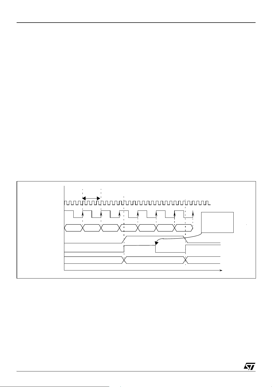
ST7LITE1
LITE TIMER (Cont’d)
11.3.3 Functional Description
11.3.3.1 Timebase Counter 1
The 8-bit value of Counter 1 cannot be read or
written by software. After an MCU reset, it starts
incrementing from 0 at a frequency of f
overflow event occurs when the counter rolls over
from F9h to 00h. If f
= 8 MHz, then the time pe-
OSC
riod between two counter overflow events is 1 ms.
This period can be doubled by setting the TB bit in
the LTCSR1 register.
OSC
/32. An
LTARR reload value. Software can write a new
value at anytime in the LTARR register, this value
will be automatically loaded in the counter when
the next overflow occurs.
When Counter 2 overflows, the TB2F bit in the
LTCSR2 register is set by hardware and an interrupt request is generated if the TB2IE bit is set.
The TB2F bit is cleared by software reading the
LTCSR2 register.
11.3.3.3 Input Capture
When Counter 1 overflows, the TB1F bit is set by
hardware and an interrupt request is generated if
the TB1IE bit is set. The TB1F bit is cleared by
software reading the LTCSR1 register.
11.3.3.2 Timebase Counter 2
Counter 2 is an 8-bit autoreload upcounter. It can
be read by accessing the LTCNTR register. After
an MCU reset, it increments at a frequency of
/32 starting from the value stored in the
f
OSC
LTARR register. A counter overflow event occurs
when the counter rolls over from FFh to the
Figure 40. Input Capture Timing Diagram.
4µs
f
CPU
f
/32
OSC
8-bit COUNTER 1
LTIC PIN
ICF FLAG
LTICR REGISTER
(@ 8MHz f
01h
)
OSC
02h 03h 05h 06h 07h
xxh
04h
The 8-bit input capture register is used to latch the
free-running upcounter (Counter 1) 1 after a rising
or falling edge is detected on the LTIC pin. When
an input capture occurs, the ICF bit is set and the
LTICR1 register contains the MSB of Counter 1.
An interrupt is generated if the ICIE bit is set. The
ICF bit is cleared by reading the LTICR register.
The LTICR is a read-only register and always contains the data from the last input capture. Input
capture is inhibited if the ICF bit is set.
CLEARED
BY S/W
READING
LTIC REGISTER
04h
07h
66/131
1
t
Page 67
LITE TIMER (Cont’d)
– The opcode for the HALT instruction is 0x8E. To
avoid an unexpected HALT instruction due to a
program counter failure, it is advised to clear all
occurrences of the data value 0x8E from memory. For example, avoid defining a constant in
ROM with the value 0x8E.
– As the HALT instruction clears the I bit in the CC
register to allow interrupts, the user may choose
to clear all pending interrupt bits before executing the HALT instruction. This avoids entering
other peripheral interrupt routines after executing
the external interrupt routine corresponding to
the wake-up event (reset or external interrupt).
ST7LITE1
11.3.6 Register Description
LITE TIMER CONTROL/STATUS REGISTER 2
(LTCSR2)
Read / Write
Reset Value: 0x00 0000 (x0h)
70
000000TB2IETB2F
11.3.4 Low Power Modes
Mode Description
No effect on Lite timer
SLOW
(this peripheral is driven directly
OSC
/32)
by f
WAIT No effect on Lite timer
ACTIVE-HALT No effect on Lite timer
HALT Lite timer stops counting
11.3.5 Interrupts
Interrupt
Event
Timebase 1
Event
Timebase 2
Event
IC Event ICF ICIE Yes No No
Event
Enable
Control
Flag
TB1F TB1IE Yes Yes No
TB2F TB2IE Yes No No
Bit
Exit
from
Wait
Exit
from
Active
Halt
Exit
from
Halt
Note: The TBxF and ICF interrupt events are con-
nected to separate interrupt vectors (see Interrupts chapter).
Bits 7:2 = Reserved, must be kept cleared.
Bit 1 = TB2IE Timebase 2 Interrupt enable.
This bit is set and cleared by software.
0: Timebase (TB2) interrupt disabled
1: Timebase (TB2) interrupt enabled
Bit 0 = TB2F Timebase 2 Interrupt Flag.
This bit is set by hardware and cleared by software
reading the LTCSR register. Writing to this bit has
no effect.
0: No Counter 2 overflow
1: A Counter 2 overflow has occurred
LITE TIMER AUTORELOAD REGISTER
(LTARR)
Read / Write
Reset Value: 0000 0000 (00h)
70
AR7 AR7 AR7 AR7 AR3 AR2 AR1 AR0
They generate an interrupt if the enable bit is set in
the LTCSR1 or LTCSR2 register and the interrupt
mask in the CC register is reset (RIM instruction).
Bits 7:0 = AR[7:0] Counter 2 Reload Value.
These bits register is read/write by software. The
LTARR value is automatically loaded into Counter
2 (LTCNTR) when an overflow occurs.
67/131
1
Page 68

ST7LITE1
LITE TIMER (Cont’d)
LITE TIMER COUNTER 2 (LTCNTR)
Read only
Reset Value: 0000 0000 (00h)
70
CNT7 CNT7 CNT7 CNT7 CNT3 CNT2 CNT1 CNT0
Bit 5 = TB Timebase period selection.
This bit is set and cleared by software.
0: Timebase period = t
1: Timebase period = t
* 8000 (1ms @ 8 MHz)
OSC
* 16000 (2ms @ 8
OSC
MHz)
Bit 4 = TB1IE Timebase Interrupt enable.
This bit is set and cleared by software.
Bits 7:0 = CNT[7:0] Counter 2 Reload Value.
This register is read by software. The LTARR val-
0: Timebase (TB1) interrupt disabled
1: Timebase (TB1) interrupt enabled
ue is automatically loaded into Counter 2 (LTCNTR) when an overflow occurs.
Bit 3 = TB1F Timebase Interrupt Flag.
This bit is set by hardware and cleared by software
LITE TIMER CONTROL/STATUS REGISTER
(LTCSR1)
Read / Write
Reset Value: 0x00 0000 (x0h)
70
reading the LTCSR register. Writing to this bit has
no effect.
0: No counter overflow
1: A counter overflow has occurred
Bits 2:0 = Reserved
ICIE ICF TB TB1IE TB1F - - -
LITE TIMER INPUT CAPTURE REGISTER
(LTICR)
Read only
Bit 7 = ICIE Interrupt Enable.
Reset Value: 0000 0000 (00h)
This bit is set and cleared by software.
0: Input Capture (IC) interrupt disabled
70
1: Input Capture (IC) interrupt enabled
ICR7 ICR6 ICR5 ICR4 ICR3 ICR2 ICR1 ICR0
Bit 6 = ICF Input Capture Flag.
This bit is set by hardware and cleared by software
by reading the LTICR register. Writing to this bit
does not change the bit value.
0: No input capture
1: An input capture has occurred
Note: After an MCU reset, software must initialise
Bits 7:0 = ICR[7:0] Input Capture Value
These bits are read by software and cleared by
hardware after a reset. If the ICF bit in the LTCSR
is cleared, the value of the 8-bit up-counter will be
captured when a rising or falling edge occurs on
the LTIC pin.
the ICF bit by reading the LTICR register
68/131
1
Page 69

LITE TIMER (Cont’d)
Table 15. Lite Timer Register Map and Reset Values
ST7LITE1
Address
(Hex.)
08
09
0A
0B
0C
Register
Label
LTCSR2
Reset Value
LTARR
Reset Value
LTCNTR
Reset Value
LTCSR1
Reset Value
LTICR
Reset Value
76543210
000000
AR7
0
CNT7
0
ICIE
0
ICR7
0
AR6
0
CNT6
0
ICF
x
ICR6
0
AR5
0
CNT5
0
TB
0
ICR5
0
AR4
0
CNT4
0
TB1IE
0
ICR4
0
AR3
0
CNT3
0
TB1F
0
ICR3
0
AR2
0
CNT2
0
000
ICR2
0
TB2IE
0
AR1
0
CNT1
0
ICR1
0
TB2F
0
AR0
0
CNT0
0
ICR0
0
69/131
1
Page 70

ST7LITE1
11.4 SERIAL PERIPHERAL INTERFACE (SPI)
11.4.1 Introduction
The Serial Peripheral Interface (SPI) allows fullduplex, synchronous, serial communication with
external devices. An SPI system may consist of a
master and one or more slaves or a system in
which devices may be either masters or slaves.
11.4.2 Main Features
■ Full duplex synchronous transfers (on 3 lines)
■ Simplex synchronous transfers (on 2 lines)
■ Master or slave operation
■ Six master mode frequencies (f
■ f
■ SS Management by software or hardware
■ Programmable clock polarity and phase
■ End of transfer interrupt flag
■ Write collision, Master Mode Fault and Overrun
/2 max. slave mode frequency (see note)
CPU
CPU
/4 max.)
flags
Note: In slave mode, continuous transmission is
not possible at maximum frequency due to the
software overhead for clearing status flags and to
initiate the next transmission sequence.
Figure 41. Serial Peripheral Interface Block Diagram
Data/Address Bus
SPIDR
Read Buffer
Read
11.4.3 General Description
Figure 41 shows the serial peripheral interface
(SPI) block diagram. There are 3 registers:
– SPI Control Register (SPICR)
– SPI Control/Status Register (SPICSR)
– SPI Data Register (SPIDR)
The SPI is connected to external devices through
3 pins:
– MISO: Master In / Slave Out data
– MOSI: Master Out / Slave In data
– SCK: Serial Clock out by SPI masters and in-
put by SPI slaves
: Slave select:
–SS
This input signal acts as a ‘chip select’ to let
the SPI master communicate with slaves individually and to avoid contention on the data
lines. Slave SS
ard I/O ports on the master
inputs can be driven by stand-
Device.
Interrupt
request
MOSI
MISO
SCK
70/131
1
SS
SOD
bit
8-Bit Shift Register
Write
MASTER
CONTROL
SERIAL CLOCK
GENERATOR
SPIF WCOL MODF
SPIE SPE
OVR SSISSMSOD
SPI
STATE
CONTROL
MSTR
SPR2
0
CPOL
SS
CPHA
SPICSR
1
0
SPICR
SPR1
07
07
SPR0
Page 71

SERIAL PERIPHERAL INTERFACE (Cont’d)
11.4.3.1 Functional Description
A basic example of interconnections between a
single master and a single slave is illustrated in
Figure 42.
The MOSI pins are connected together and the
MISO pins are connected together. In this way
data is transferred serially between master and
slave (most significant bit first).
The communication is always initiated by the master. When the master device transmits data to a
slave device via MOSI pin, the slave device re-
Figure 42. Single Master/ Single Slave Application
ST7LITE1
sponds by sending data to the master device via
the MISO pin. This implies full duplex communication with both data out and data in synchronized
with the same clock signal (which is provided by
the master device via the SCK pin).
To use a single data line, the MISO and MOSI pins
must be connected at each node ( in this case only
simplex communication is possible).
Four possible data/clock timing relationships may
be chosen (see Figure 45) but master and slave
must be programmed with the same timing mode.
MASTER
MSBit LSBit MSBit LSBit
+5V
MISO
MOSI
SCK
SS
8-BIT SHIFT REGISTER
8-BIT SHIFT REGISTER
SPI
CLOCK
GENERATOR
MISO
MOSI
SCK
SS
SLAVE
Not used if SS is managed
by software
71/131
1
Page 72

ST7LITE1
SERIAL PERIPHERAL INTERFACE (Cont’d)
11.4.3.2 Slave Select Management
As an alternative to using the SS
Slave Select signal, the application can choose to
manage the Slave Select signal by software. This
is configured by the SSM bit in the SPICSR register (see Figure 44)
In software management, the external SS
free for other application uses and the internal SS
signal level is driven by writing to the SSI bit in the
SPICSR register.
In Master mode:
–SS
internal must be held high continuously
pin to control the
pin is
In Slave Mode:
There are two cases depending on the data/clock
timing relationship (see Figure 43):
If CPHA=1 (data latched on 2nd clock edge):
–SS
internal must be held low during the entire
transmission. This implies that in single slave
applications the SS
V
, or made free for standard I/O by manag-
SS
ing the SS
function by software (SSM= 1 and
pin either can be tied to
SSI=0 in the in the SPICSR register)
If CPHA=0 (data latched on 1st clock edge):
–SS
internal must be held low during byte
transmission and pulled high between each
byte to allow the slave to write to the shift register. If SS
is not pulled high, a Write Collision
error will occur when the slave writes to the
shift register (see Section 11.4.5.3).
Figure 43. Generic SS
MOSI/MISO
Master SS
Slave SS
(if CPHA=0)
Slave SS
(if CPHA=1)
Timing Diagram
Byte 1 Byte 2
Figure 44. Hardware/Software Slave Select Management
SSM bit
external pin
SS
SSI bit
1
0
SS internal
Byte 3
72/131
1
Page 73

SERIAL PERIPHERAL INTERFACE (Cont’d)
11.4.3.3 Master Mode Operation
In master mode, the serial clock is output on the
SCK pin. The clock frequency, polarity and phase
are configured by software (refer to the description
of the SPICSR register).
Note: The idle state of SCK must correspond to
the polarity selected in the SPICSR register (by
pulling up SCK if CPOL=1 or pulling down SCK if
CPOL=0).
To operate the SPI in master mode, perform the
following steps in order (if the SPICSR register is
not written first, the SPICR register setting (MSTR
bit ) may be not taken into account):
1. Write to the SPICR register:
– Select the clock frequency by configuring the
SPR[2:0] bits.
– Select the clock polarity and clock phase by
configuring the CPOL and CPHA bits. Figure
45 shows the four possible configurations.
Note: The slave must have the same CPOL
and CPHA settings as the master.
2. Write to the SPICSR register:
– Either set the SSM bit and set the SSI bit or
clear the SSM bit and tie the SS
the complete byte transmit sequence.
3. Write to the SPICR register:
– Set the MSTR and SPE bits
Note: MSTR and SPE bits remain set only if
SS
is high.
The transmit sequence begins when software
writes a byte in the SPIDR register.
11.4.3.4 Master Mode Transmit Sequence
When software writes to the SPIDR register, the
data byte is loaded into the 8-bit shift register and
then shifted out serially to the MOSI pin most significant bit first.
When data transfer is complete:
– The SPIF bit is set by hardware
– An interrupt request is generated if the SPIE
bit is set and the interrupt mask in the CCR
register is cleared.
Clearing the SPIF bit is performed by the following
software sequence:
1. An access to the SPICSR register while the
SPIF bit is set
2. A read to the SPIDR register.
pin high for
ST7LITE1
Note: While the SPIF bit is set, all writes to the
SPIDR register are inhibited until the SPICSR register is read.
11.4.3.5 Slave Mode Operation
In slave mode, the serial clock is received on the
SCK pin from the master device.
To operate the SPI in slave mode:
1. Write to the SPICSR register to perform the following actions:
– Select the clock polarity and clock phase by
configuring the CPOL and CPHA bits (see
Figure 45).
Note: The slave must have the same CPOL
and CPHA settings as the master.
– Manage the SS
11.4.3.2 and Figure 43. If CPHA=1 SS
be held low continuously. If CPHA=0 SS
be held low during byte transmission and
pulled up between each byte to let the slave
write in the shift register.
2. Write to the SPICR register to clear the MSTR
bit and set the SPE bit to enable the SPI I/O
functions.
11.4.3.6 Slave Mode Transmit Sequence
When software writes to the SPIDR register, the
data byte is loaded into the 8-bit shift register and
then shifted out serially to the MISO pin most significant bit first.
The transmit sequence begins when the slave device receives the clock signal and the most significant bit of the data on its MOSI pin.
When data transfer is complete:
– The SPIF bit is set by hardware
– An interrupt request is generated if SPIE bit is
set and interrupt mask in the CCR register is
cleared.
Clearing the SPIF bit is performed by the following
software sequence:
1. An access to the SPICSR register while the
SPIF bit is set.
2. A write or a read to the SPIDR register.
Notes: While the SPIF bit is set, all writes to the
SPIDR register are inhibited until the SPICSR register is read.
The SPIF bit can be cleared during a second
transmission; however, it must be cleared before
the second SPIF bit in order to prevent an Overrun
condition (see Section 11.4.5.2).
pin as described in Section
must
must
73/131
1
Page 74
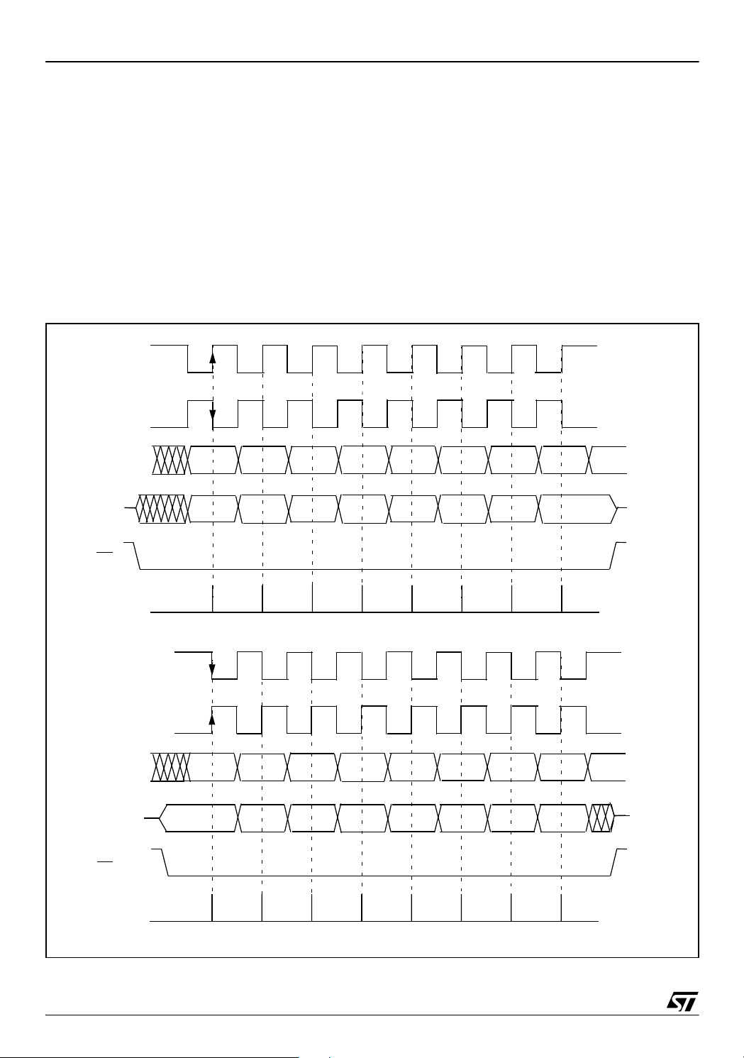
ST7LITE1
SERIAL PERIPHERAL INTERFACE (Cont’d)
11.4.4 Clock Phase and Clock Polarity
Four possible timing relationships may be chosen
by software, using the CPOL and CPHA bits (See
Figure 45).
Note: The idle state of SCK must correspond to
the polarity selected in the SPICSR register (by
pulling up SCK if CPOL=1 or pulling down SCK if
CPOL=0).
The combination of the CPOL clock polarity and
CPHA (clock phase) bits selects the data capture
clock edge
Figure 45. Data Clock Timing Diagram
SCK
(CPOL = 1)
SCK
(CPOL = 0)
Figure 45, shows an SPI transfer with the four
combinations of the CPHA and CPOL bits. The diagram may be interpreted as a master or slave
timing diagram where the SCK pin, the MISO pin,
the MOSI pin are directly connected between the
master and the slave device.
Note: If CPOL is changed at the communication
byte boundaries, the SPI must be disabled by resetting the SPE bit.
CPHA =1
MISO
(from master)
MOSI
(from slave)
SS
(to slave)
CAPTURE STROBE
SCK
(CPOL = 1)
SCK
(CPOL = 0)
MISO
(from master)
MOSI
(from slave)
SS
(to slave)
CAPTURE STROBE
MSBit Bit 6 Bit 5
MSBit Bit 6 Bit 5
MSBit Bit 6 Bit 5
MSBit Bit 6 Bit 5
Bit 4 Bit3 Bit 2 Bit 1 LSBit
Bit 4 Bit3Bit 2Bit 1LSBit
CPHA =0
Bit 4 Bit3 Bit 2 Bit 1 LSBit
Bit 4 Bit3 Bit 2 Bit 1 LSBit
74/131
1
Note:
This figure should not be used as a replacement for parametric information.
Refer to the Electrical Characteristics chapter.
Page 75
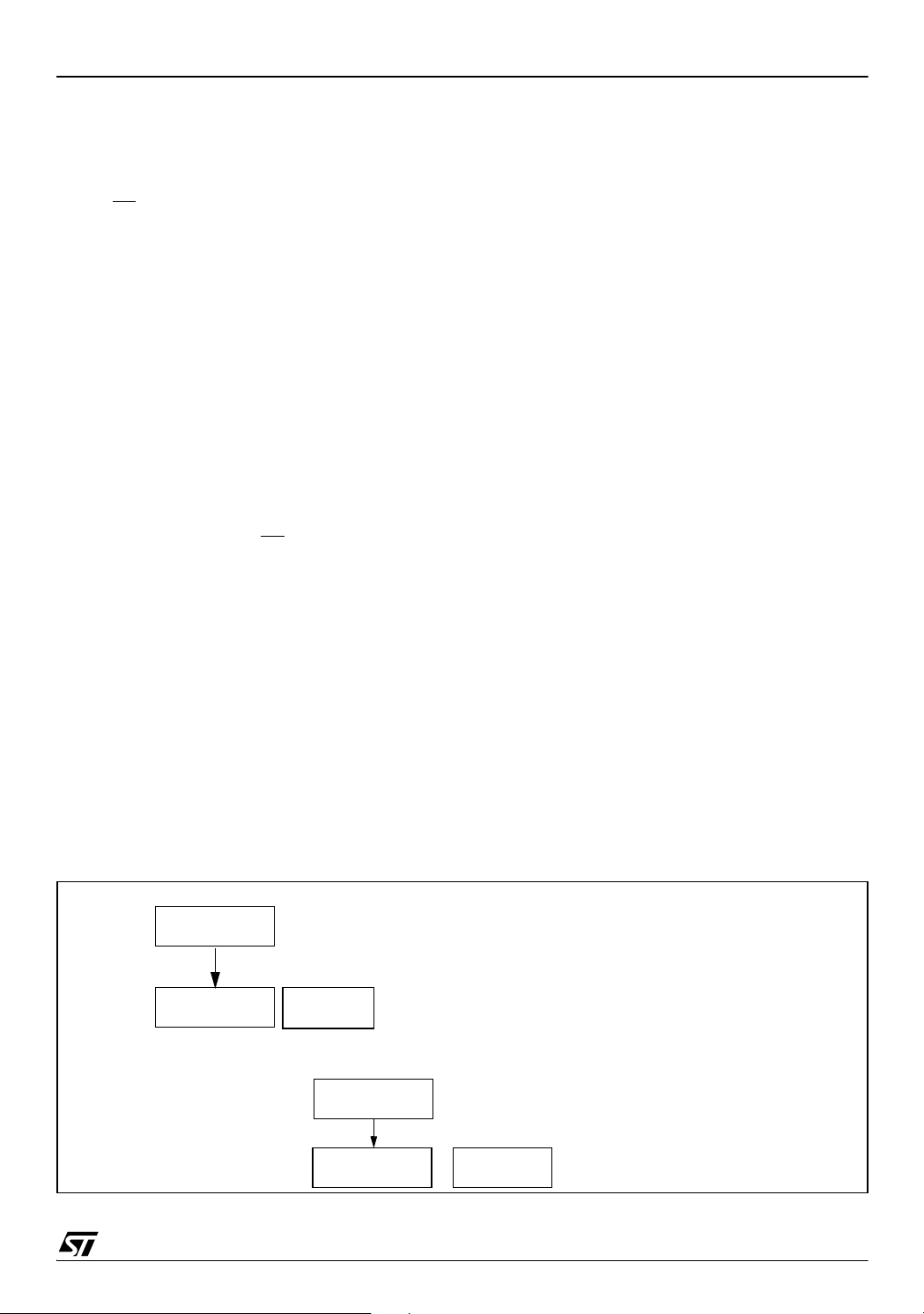
SERIAL PERIPHERAL INTERFACE (Cont’d)
11.4.5 Error Flags
11.4.5.1 Master Mode Fault (MODF)
Master mode fault occurs when the master device
has its SS
pin pulled low.
When a Master mode fault occurs:
– The MODF bit is set and an SPI interrupt re-
quest is generated if the SPIE bit is set.
– The SPE bit is reset. This blocks all output
from the Device and disables the SPI peripheral.
– The MSTR bit is reset, thus forcing the Device
into slave mode.
Clearing the MODF bit is done through a software
sequence:
1. A read access to the SPICSR register while the
MODF bit is set.
2. A write to the SPICR register.
Notes: To avoid any conflicts in an application
with multiple slaves, the SS
pin must be pulled
high during the MODF bit clearing sequence. The
SPE and MSTR bits may be restored to their original state during or after this clearing sequence.
Hardware does not allow the user to set the SPE
and MSTR bits while the MODF bit is set except in
the MODF bit clearing sequence.
In a slave device, the MODF bit can not be set, but
in a multi master configuration the
Device can be in
slave mode with the MODF bit set.
The MODF bit indicates that there might have
been a multi-master conflict and allows software to
handle this using an interrupt routine and either
perform to a reset or return to an application default state.
ST7LITE1
11.4.5.2 Overrun Condition (OVR)
An overrun condition occurs, when the master device has sent a data byte and the slave device has
not cleared the SPIF bit issued from the previously
transmitted byte.
When an Overrun occurs:
– The OVR bit is set and an interrupt request is
generated if the SPIE bit is set.
In this case, the receiver buffer contains the byte
sent after the SPIF bit was last cleared. A read to
the SPIDR register returns this byte. All other
bytes are lost.
The OVR bit is cleared by reading the SPICSR
register.
11.4.5.3 Write Collision Error (WCOL)
A write collision occurs when the software tries to
write to the SPIDR register while a data transfer is
taking place with an external device. When this
happens, the transfer continues uninterrupted;
and the software write will be unsuccessful.
Write collisions can occur both in master and slave
mode. See also Section 11.4.3.2 Slave Select
Management.
Note: a "read collision" will never occur since the
received data byte is placed in a buffer in which
access is always synchronous with the CPU operation.
The WCOL bit in the SPICSR register is set if a
write collision occurs.
No SPI interrupt is generated when the WCOL bit
is set (the WCOL bit is a status flag only).
Clearing the WCOL bit is done through a software
sequence (see Figure 46).
Figure 46. Clearing the WCOL bit (Write Collision Flag) Software Sequence
Clearing sequence after SPIF = 1 (end of a data byte transfer)
1st Step
2nd Step
Read SPICSR
Read SPIDR
RESULT
SPIF =0
WCOL=0
Clearing sequence before SPIF = 1 (during a data byte transfer)
1st Step
2nd Step
Read SPICSR
Read SPIDR
RESULT
WCOL=0
Note: Writing to the SPIDR register instead of reading it does not
reset the WCOL bit
75/131
1
Page 76
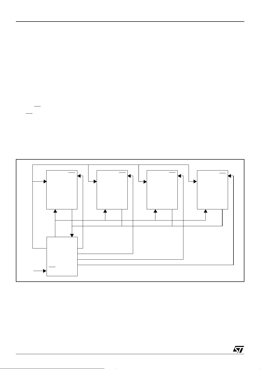
ST7LITE1
SERIAL PERIPHERAL INTERFACE (Cont’d)
11.4.5.4 Single Master and Multimaster Configurations
There are two types of SPI systems:
– Single Master System
– Multimaster System
Single Master System
A typical single master system may be configured,
using a
slaves (see Figure 47).
The master device selects the individual slave devices by using four pins of a parallel port to control
the four SS
The SS
master device ports will be forced to be inputs at
that time, thus disabling the slave devices.
Note: To prevent a bus conflict on the MISO line
the master allows only one active slave device
during a transmission.
Figure 47. Single Master / Multiple Slave Configuration
device as the master and four devices as
pins of the slave devices.
pins are pulled high during reset since the
For more security, the slave device may respond
to the master with the received data byte. Then the
master will receive the previous byte back from the
slave device if all MISO and MOSI pins are connected and the slave has not written to its SPIDR
register.
Other transmission security methods can use
ports for handshake lines or data bytes with command fields.
Multi-Master System
A multi-master system may also be configured by
the user. Transfer of master control could be implemented using a handshake method through the
I/O ports or by an exchange of code messages
through the serial peripheral interface system.
The multi-master system is principally handled by
the MSTR bit in the SPICR register and the MODF
bit in the SPICSR register.
5V
SCK
Device
MOSI
MOSI
SCK
Master
Device
SS
Slave
MISO
SS
Ports
SCK
MOSI MOSI MOSIMISO MISO MISOMISO
Slave
Device
SS
SCK
Slave
Device
SS
SS
SCK
Slave
Device
76/131
1
Page 77
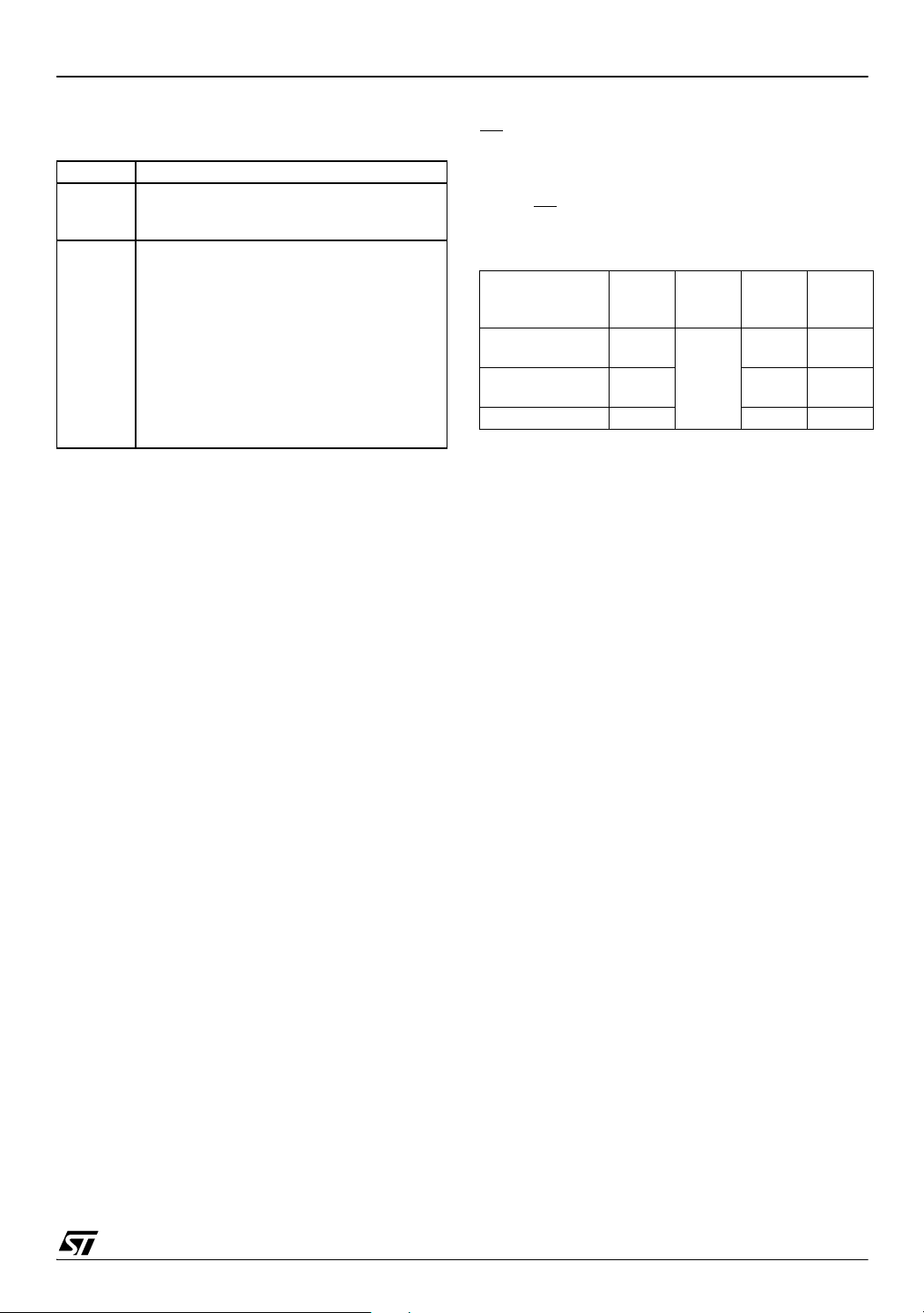
SERIAL PERIPHERAL INTERFACE (Cont’d)
11.4.6 Low Power Modes
Mode Description
WAIT
HALT
No effect on SPI.
SPI interrupt events cause the Device to exit
from WAIT mode.
SPI registers are frozen.
In HALT mode, the SPI is inactive. SPI operation resumes when the Device is woken up
by an interrupt with “exit from HALT mode”
capability. The data received is subsequently
read from the SPIDR register when the software is running (interrupt vector fetching). If
several data are received before the wakeup event, then an overrun error is generated.
This error can be detected after the fetch of
the interrupt routine that woke up the Device.
11.4.6.1 Using the SPI to wake-up the Device from Halt mode
In slave configuration, the SPI is able to wake-up
the Device from HALT mode through a SPIF interrupt. The data received is subsequently read from
the SPIDR register when the software is running
(interrupt vector fetch). If multiple data transfers
have been performed before software clears the
SPIF bit, then the OVR bit is set by hardware.
Note: When waking up from Halt mode, if the SPI
remains in Slave mode, it is recommended to perform an extra communications cycle to bring the
SPI from Halt mode state to normal state. If the
SPI exits from Slave mode, it returns to normal
state immediately.
Caution: The SPI can wake-up the
Device from
Halt mode only if the Slave Select signal (external
ST7LITE1
pin or the SSI bit in the SPICSR register) is low
SS
when the
lection is configured as external (see Section
11.4.3.2), make sure the master drives a low level
on the SS
11.4.7 Interrupts
Interrupt Event
SPI End of Transfer Event
Master Mode
Fault Event
Overrun Error OVR Yes No
Note: The SPI interrupt events are connected to
the same interrupt vector (see Interrupts chapter).
They generate an interrupt if the corresponding
Enable Control Bit is set and the interrupt mask in
the CC register is reset (RIM instruction).
Device enters Halt mode. So if Slave se-
pin when the slave enters Halt mode.
Event
Flag
SPIF
MODF Yes No
Enable
Control
Bit
SPIE
Exit
from
Wait
Yes Yes
Exit
from
Halt
77/131
1
Page 78
ST7LITE1
SERIAL PERIPHERAL INTERFACE (Cont’d)
11.4.8 Register Description CONTROL REGISTER (SPICR)
Read/Write
Reset Value: 0000 xxxx (0xh)
70
SPIE SPE SPR2 MSTR CPOL CPHA SPR1 SPR0
Bit 7 = SPIE Serial Peripheral Interrupt Enable.
This bit is set and cleared by software.
0: Interrupt is inhibited
1: An SPI interrupt is generated whenever an End
of Transfer event, Master Mode Fault or Overrun error occurs (SPIF=1, MODF=1 or OVR=1
in the SPICSR register)
Bit 6 = SPE Serial Peripheral Output Enable.
This bit is set and cleared by software. It is also
cleared by hardware when, in master mode, SS
=0
(see Section 11.4.5.1 Master Mode Fault
(MODF)). The SPE bit is cleared by reset, so the
SPI peripheral is not initially connected to the external pins.
0: I/O pins free for general purpose I/O
1: SPI I/O pin alternate functions enabled
Bit 5 = SPR2 Divider Enable.
This bit is set and cleared by software and is
cleared by reset. It is used with the SPR[1:0] bits to
set the baud rate. Refer to Table 16 SPI Master
mode SCK Frequency.
0: Divider by 2 enabled
1: Divider by 2 disabled
Note: This bit has no effect in slave mode.
Bit 4 = MSTR Master Mode.
This bit is set and cleared by software. It is also
cleared by hardware when, in master mode, SS
=0
(see Section 11.4.5.1 Master Mode Fault
(MODF)).
0: Slave mode
1: Master mode. The function of the SCK pin
changes from an input to an output and the functions of the MISO and MOSI pins are reversed.
Bit 3 = CPOL Clock Polarity.
This bit is set and cleared by software. This bit determines the idle state of the serial Clock. The
CPOL bit affects both the master and slave
modes.
0: SCK pin has a low level idle state
1: SCK pin has a high level idle state
Note: If CPOL is changed at the communication
byte boundaries, the SPI must be disabled by resetting the SPE bit.
Bit 2 = CPHA Clock Phase.
This bit is set and cleared by software.
0: The first clock transition is the first data capture
edge.
1: The second clock transition is the first capture
edge.
Note: The slave must have the same CPOL and
CPHA settings as the master.
Bits 1:0 = SPR[1:0] Serial Clock Frequency.
These bits are set and cleared by software. Used
with the SPR2 bit, they select the baud rate of the
SPI serial clock SCK output by the SPI in master
mode.
Note: These 2 bits have no effect in slave mode.
Table 16. SPI Master mode SCK Frequency
Serial Clock SPR2 SPR1 SPR0
f
/4 1 0 0
CPU
f
/8 0 0 0
CPU
f
/16 0 0 1
CPU
f
/32 1 1 0
CPU
f
/64 0 1 0
CPU
f
/128 0 1 1
CPU
78/131
1
Page 79

SERIAL PERIPHERAL INTERFACE (Cont’d)
CONTROL/STATUS REGISTER (SPICSR)
Read/Write (some bits Read Only)
Reset Value: 0000 0000 (00h)
70
Bit 2 = SOD SPI Output Disable.
This bit is set and cleared by software. When set, it
disables the alternate function of the SPI output
(MOSI in master mode / MISO in slave mode)
SPIF WCOL OVR MODF - SOD SSM SSI
0: SPI output enabled (if SPE=1)
1: SPI output disabled
ST7LITE1
Bit 7 = SPIF Serial Peripheral Data Transfer Flag
(Read only).
This bit is set by hardware when a transfer has
been completed. An interrupt is generated if
SPIE=1 in the SPICR register. It is cleared by a
software sequence (an access to the SPICSR
register followed by a write or a read to the
SPIDR register).
0: Data transfer is in progress or the flag has been
cleared.
1: Data transfer between the
Device and an exter-
nal device has been completed.
Note: While the SPIF bit is set, all writes to the
SPIDR register are inhibited until the SPICSR register is read.
Bit 6 = WCOL Write Collision status (Read only).
This bit is set by hardware when a write to the
SPIDR register is done during a transmit sequence. It is cleared by a software sequence (see
Figure 46).
0: No write collision occurred
1: A write collision has been detected
Bit 5 = OVR SPI Overrun error (Read only).
This bit is set by hardware when the byte currently
being received in the shift register is ready to be
transferred into the SPIDR register while SPIF = 1
(See Section 11.4.5.2). An interrupt is generated if
SPIE = 1 in the SPICR register. The OVR bit is
cleared by software reading the SPICSR register.
0: No overrun error
1: Overrun error detected
Bit 4 = MODF Mode Fault flag (Read only).
This bit is set by hardware when the SS
pin is
pulled low in master mode (see Section 11.4.5.1
Master Mode Fault (MODF)). An SPI interrupt can
be generated if SPIE=1 in the SPICR register. This
bit is cleared by a software sequence (An access
to the SPICSR register while MODF=1 followed by
a write to the SPICR register).
0: No master mode fault detected
1: A fault in master mode has been detected
Bit 3 = Reserved, must be kept cleared.
Bit 1 = SSM SS
Management.
This bit is set and cleared by software. When set, it
disables the alternate function of the SPI SS
pin
and uses the SSI bit value instead. See Section
11.4.3.2 Slave Select Management.
0: Hardware management (SS
managed by exter-
nal pin)
1: Software management (internal SS
trolled by SSI bit. External SS
signal con-
pin free for gener-
al-purpose I/O)
Bit 0 = SSI SS
Internal Mode.
This bit is set and cleared by software. It acts as a
‘chip select’ by controlling the level of the SS
slave
select signal when the SSM bit is set.
0 : Slave selected
1 : Slave deselected
DATA I/O REGISTER (SPIDR)
Read/Write
Reset Value: Undefined
70
D7 D6 D5 D4 D3 D2 D1 D0
The SPIDR register is used to transmit and receive
data on the serial bus. In a master device, a write
to this register will initiate transmission/reception
of another byte.
Notes: During the last clock cycle the SPIF bit is
set, a copy of the received data byte in the shift
register is moved to a buffer. When the user reads
the serial peripheral data I/O register, the buffer is
actually being read.
While the SPIF bit is set, all writes to the SPIDR
register are inhibited until the SPICSR register is
read.
Warning: A write to the SPIDR register places
data directly into the shift register for transmission.
A read to the SPIDR register returns the value located in the buffer and not the content of the shift
register (see Figure 41).
79/131
1
Page 80

ST7LITE1
Table 17. SPI Register Map and Reset Values
Address
(Hex.)
0031h
0032h
0033h
Register
Label
SPIDR
Reset Value
SPICR
Reset Value
SPICSR
Reset Value
76543210
MSB
xxxxxxx
SPIE
0
SPIF
0
SPE
0
WCOL
0
SPR20MSTR0CPOL
x
OVR
0
MODF
00
CPHA
x
SOD
0
SPR1
x
SSM
0
LSB
x
SPR0
x
SSI
0
80/131
1
Page 81
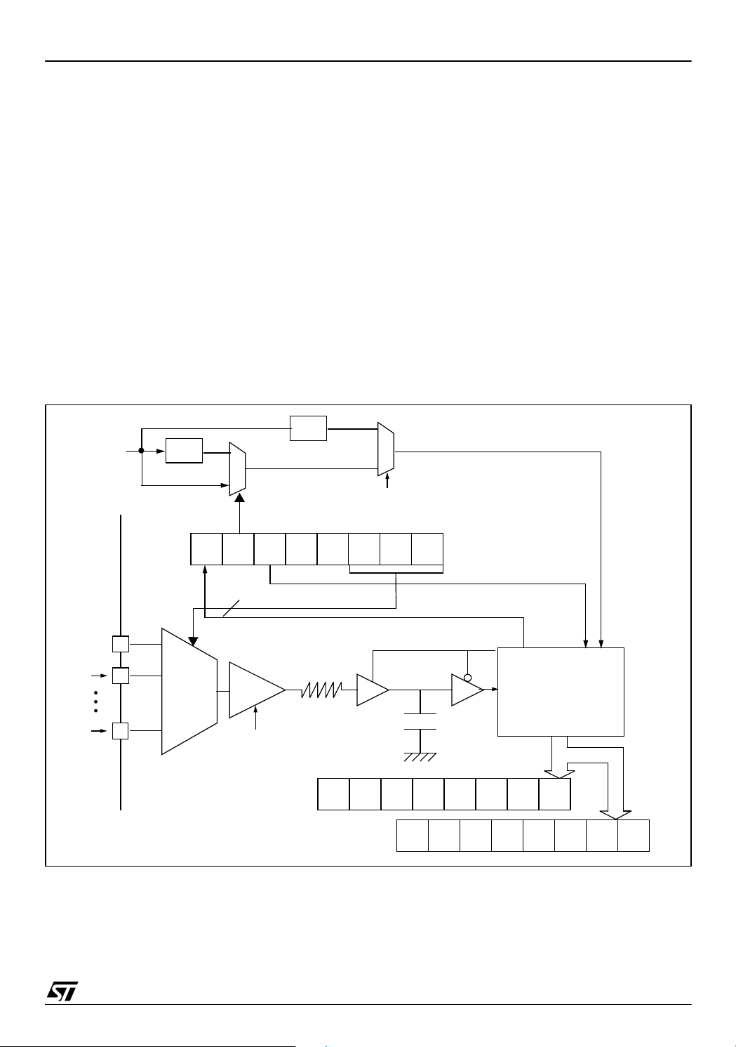
11.5 10-BIT A/D CONVERTER (ADC)
ST7LITE1
11.5.1 Introduction
The on-chip Analog to Digital Converter (ADC) peripheral is a 10-bit, successive approximation converter with internal sample and hold circuitry. This
peripheral has up to 7 multiplexed analog input
channels (refer to device pin out description) that
allow the peripheral to convert the analog voltage
levels from up to 7 different sources.
The result of the conversion is stored in a 10-bit
Data Register. The A/D converter is controlled
through a Control/Status Register.
11.5.2 Main Features
■ 10-bit conversion
■ Up to 7 channels with multiplexed input
■ Linear successive approximation
Figure 48. ADC Block Diagram
f
CPU
DIV 2
0
1
DIV 4
■ Data register (DR) which contains the results
■ Conversion complete status flag
■ On/off bit (to reduce consumption)
The block diagram is shown in Figure 48.
11.5.3 Functional Description
11.5.3.1 Analog Power Supply
V
DDA
and V
are the high and low level refer-
SSA
ence voltage pins. In some devices (refer to device
pin out description) they are internally connected
to the V
and VSS pins.
DD
Conversion accuracy may therefore be impacted
by voltage drops and noise in the event of heavily
loaded or badly decoupled power supply lines.
1
0
SLOW
bit
f
ADC
AIN0
AIN1
AINx
ANALOG
MUX
3
x 1 or
x 8
AMPSEL
bit
ADCDRH
0
R
CH2 CH1EOC SPEED ADON 0 CH0
HOLD CONTROL
ADC
ADCCSR
C
ADC
ADCDRL 00 0
ANALOG TO DIGITAL
CONVERTER
D4 D3D5D9 D8 D7 D6 D2
AMP
CAL
SLOW
AMP
SEL
D1 D0
81/131
1
Page 82

ST7LITE1
10-BIT A/D CONVERTER (ADC) (Cont’d)
11.5.3.2 Input Voltage Amplifier
The input voltage can be amplified by a factor of 8
by enabling the AMPSEL bit in the ADCDRL register.
When the amplifier is enabled, the input range is
0V to V
For example, if V
vert voltages in the range 0V to 430mV with an
ideal resolution of 0.6mV (equivalent to 13-bit resolution with reference to a V
For more details, refer to the Electrical characteristics section.
Note: The amplifier is switched on by the ADON
bit in the ADCCSR register, so no additional startup time is required when the amplifier is selected
by the AMPSEL bit.
11.5.3.3 Digital A/D Conversion Result
The conversion is monotonic, meaning that the result never decreases if the analog input does not
and never increases if the analog input does not.
If the input voltage (V
(high-level voltage reference) then the conversion
result is FFh in the ADCDRH register and 03h in
the ADCDRL register (without overflow indication).
If the input voltage (V
level voltage reference) then the conversion result
in the ADCDRH and ADCDRL registers is 00 00h.
The A/D converter is linear and the digital result of
the conversion is stored in the ADCDRH and ADCDRL registers. The accuracy of the conversion is
described in the Electrical Characteristics Section.
R
AIN
for an analog input signal. If the impedance is too
high, this will result in a loss of accuracy due to
leakage and sampling not being completed in the
alloted time.
11.5.3.4 A/D Conversion
The analog input ports must be configured as input, no pull-up, no interrupt. Refer to the «I/O
ports» chapter. Using these pins as analog inputs
does not affect the ability of the port to be read as
a logic input.
In the ADCCSR register:
– Select the CS[2:0] bits to assign the analog
/8.
DD
= 5V, then the ADC can con-
DD
to VDD range).
SS
) is greater than V
AIN
) is lower than V
AIN
SSA
DDA
(low-
is the maximum recommended impedance
channel to convert.
ADC Conversion mode
In the ADCCSR register:
Set the ADON bit to enable the A/D converter and
to start the conversion. From this time on, the
ADC performs a continuous conversion of the
selected channel.
When a conversion is complete:
– The EOC bit is set by hardware.
– The result is in the ADCDR registers.
A read to the ADCDRH resets the EOC bit.
To read the 10 bits, perform the following steps:
1. Poll EOC bit
2. Read ADCDRL
3. Read ADCDRH. This clears EOC automati-
cally.
To read only 8 bits, perform the following steps:
1. Poll EOC bit
2. Read ADCDRH. This clears EOC automati-
cally.
11.5.4 Low Power Modes Note: The A/D converter may be disabled by re-
setting the ADON bit. This feature allows reduced
power consumption when no conversion is needed and between single shot conversions.
Mode Description
WAIT No effect on A/D Converter
A/D Converter disabled.
After wakeup from Halt mode, the A/D
HALT
Converter requires a stabilization time
(see Electrical Characteristics)
t
STAB
before accurate conversions can be
performed.
11.5.5 Interrupts
None.
82/131
1
Page 83

10-BIT A/D CONVERTER (ADC) (Cont’d)
11.5.6 Register Description
ST7LITE1
CONTROL/STATUS REGISTER (ADCCSR)
Read/Write (Except bit 7 read only)
Reset Value: 0000 0000 (00h)
70
EOC SPEED ADON 0 CH3 CH2 CH1 CH0
DATA REGISTER HIGH (ADCDRH)
Read Only
Reset Value: xxxx xxxx (xxh)
70
D9 D8 D7 D6 D5 D4 D3 D2
Bit 7 = EOC End of Conversion
This bit is set by hardware. It is cleared by software reading the ADCDRH register.
Bit 7:0 = D[9:2] MSB of Analog Converted Value
0: Conversion is not complete
1: Conversion complete
AMP CONTROL/DATA REGISTER LOW (ADCDRL)
Bit 6 = SPEED ADC clock selection
This bit is set and cleared by software. It is used
Read/Write
Reset Value: 0000 00xx (0xh)
together with the SLOW bit to configure the ADC
clock speed. Refer to the table in the SLOW bit de-
70
scription.
AMP
CAL
SLOW
Bit 5 = ADON A/D Converter on
This bit is set and cleared by software.
000
Bit 7:5 = Reserved. Forced by hardware to 0.
0: A/D converter and amplifier are switched off
1: A/D converter and amplifier are switched on
Bit 4 = AMPCAL Amplifier Calibration Bit
This bit is set and cleared by software. User is sug-
Bit 4:3 = Reserved. Must be kept cleared.
gested to use this bit to calibrate the ADC when
amplifier is ON. Setting this bit internally connects
amplifier input to 0v. Hence, corresponding ADC
Bit 2:0 = CH[2:0] Channel Selection
These bits are set and cleared by software. They
select the analog input to convert.
Channel Pin* CH2 CH1 CH0
AIN0 0 0 0
AIN1 0 0 1
AIN2 0 1 0
AIN3 0 1 1
AIN4 1 0 0
AIN5 1 0 1
AIN6 1 1 0
*The number of channels is device dependent. Refer to
the device pinout description.
output can be used in software to eliminate amplifier-offset error.
0: Calibration off
1: Calibration on. (The input voltage of the amp is
set to 0V)
Note: It is advised to use this bit to calibrate the
ADC when the amplifier is ON. Setting this bit internally connects the amplifier input to 0v. Hence,
the corresponding ADC output can be used in software to eliminate an amplifier-offset error.
Bit 3 = SLOW Slow mode
This bit is set and cleared by software. It is used
together with the SPEED bit to configure the ADC
clock speed as shown on the table below.
AMP-
SEL
D1 D0
f
ADC
f
/2 00
CPU
f
CPU
f
/4 1x
CPU
SLOW SPEED
01
83/131
1
Page 84

ST7LITE1
Bit 2 = AMPSEL Amplifier Selection Bit
This bit is set and cleared by software.
0: Amplifier is not selected
1: Amplifier is selected
Table 18. ADC Register Map and Reset Values
Address
(Hex.)
0034h
0035h
0036h
Register
Label
ADCCSR
Reset Value
ADCDRH
Reset Value
ADCDRL
Reset Value
76543210
EOC0SPEED0ADON
D9
x
0
0
D8
x
0
0
Note: When AMPSEL=1 it is mandatory that f
be less than or equal to 2 MHz.
Bit 1:0 = D[1:0] LSB of Analog Converted Value
D7
0
0
x
0
0
0
D6
x
AMPCAL0SLOW0AMPSEL0D1
0
0
D5
x
CH2
0
D4
x
CH1
0
D3
x
x
ADC
CH0
0
D2
x
D0
x
84/131
1
Page 85

12 INSTRUCTION SET
ST7LITE1
12.1 ST7 ADDRESSING MODES
The ST7 Core features 17 different addressing
modes which can be classified in 7 main groups:
Addressing Mode Example
Inherent nop
Immediate ld A,#$55
Direct ld A,$55
Indexed ld A,($55,X)
Indirect ld A,([$55],X)
Relative jrne loop
Bit operation bset byte,#5
so, most of the addressing modes may be subdivided in two sub-modes called long and short:
– Long addressing mode is more powerful be-
cause it can use the full 64 Kbyte address space,
however it uses more bytes and more CPU cycles.
– Short addressing mode is less powerful because
it can generally only access page zero (0000h 00FFh range), but the instruction size is more
compact, and faster. All memory to memory instructions use short addressing modes only
(CLR, CPL, NEG, BSET, BRES, BTJT, BTJF,
INC, DEC, RLC, RRC, SLL, SRL, SRA, SWAP)
The ST7 Assembler optimizes the use of long and
short addressing modes.
The ST7 Instruction set is designed to minimize
the number of bytes required per instruction: To do
Table 19. ST7 Addressing Mode Overview
Mode Syntax
Inherent nop + 0
Immediate ld A,#$55 + 1
Short Direct ld A,$10 00..FF + 1
Long Direct ld A,$1000 0000..FFFF + 2
No Offset Direct Indexed ld A,(X) 00..FF
Short Direct Indexed ld A,($10,X) 00..1FE + 1
Long Direct Indexed ld A,($1000,X) 0000..FFFF + 2
Short Indirect ld A,[$10] 00..FF 00..FF byte + 2
Long Indirect ld A,[$10.w] 0000..FFFF 00..FF word + 2
Short Indirect Indexed ld A,([$10],X) 00..1FE 00..FF byte + 2
Long Indirect Indexed ld A,([$10.w],X) 0000..FFFF 00..FF word + 2
Relative Direct jrne loop PC-128/PC+127
Relative Indirect jrne [$10] PC-128/PC+127
Bit Direct bset $10,#7 00..FF + 1
Bit Indirect bset [$10],#7 00..FF 00..FF byte + 2
Bit Direct Relative btjt $10,#7,skip 00..FF + 2
Bit Indirect Relative btjt [$10],#7,skip 00..FF 00..FF byte + 3
Destination/
Source
Pointer
Address
(Hex.)
1)
1)
00..FF byte + 2
Pointer
Size
(Hex.)
Length
(Bytes)
+ 0 (with X register)
+ 1 (with Y register)
+ 1
Note 1. At the time the instruction is executed, the Program Counter (PC) points to the instruction following JRxx.
85/131
1
Page 86

ST7LITE1
ST7 ADDRESSING MODES (Cont’d)
12.1.1 Inherent
All Inherent instructions consist of a single byte.
The opcode fully specifies all the required information for the CPU to process the operation.
Inherent Instruction Function
NOP No operation
TRAP S/W Interrupt
WFI
HALT
RET Sub-routine Return
IRET Interrupt Sub-routine Return
SIM Set Interrupt Mask
RIM Reset Interrupt Mask
SCF Set Carry Flag
RCF Reset Carry Flag
RSP Reset Stack Pointer
LD Load
CLR Clear
PUSH/POP Push/Pop to/from the stack
INC/DEC Increment/Decrement
TNZ Test Negative or Zero
CPL, NEG 1 or 2 Complement
MUL Byte Multiplication
SLL, SRL, SRA, RLC,
RRC
SWAP Swap Nibbles
12.1.2 Immediate
Immediate instructions have two bytes, the first
byte contains the opcode, the second byte contains the operand value.
Immediate Instruction Function
LD Load
CP Compare
BCP Bit Compare
AND, OR, XOR Logical Operations
ADC, ADD, SUB, SBC Arithmetic Operations
Wait For Interrupt (Low Power
Mode)
Halt Oscillator (Lowest Power
Mode)
Shift and Rotate Operations
12.1.3 Direct
In Direct instructions, the operands are referenced
by their memory address.
The direct addressing mode consists of two submodes:
Direct (short)
The address is a byte, thus requires only one byte
after the opcode, but only allows 00 - FF addressing space.
Direct (long)
The address is a word, thus allowing 64 Kbyte addressing space, but requires 2 bytes after the opcode.
12.1.4 Indexed (No Offset, Short, Long)
In this mode, the operand is referenced by its
memory address, which is defined by the unsigned
addition of an index register (X or Y) with an offset.
The indirect addressing mode consists of three
sub-modes:
Indexed (No Offset)
There is no offset, (no extra byte after the opcode),
and allows 00 - FF addressing space.
Indexed (Short)
The offset is a byte, thus requires only one byte after the opcode and allows 00 - 1FE addressing
space.
Indexed (long)
The offset is a word, thus allowing 64 Kbyte addressing space and requires 2 bytes after the opcode.
12.1.5 Indirect (Short, Long)
The required data byte to do the operation is found
by its memory address, located in memory (pointer).
The pointer address follows the opcode. The indirect addressing mode consists of two sub-modes:
Indirect (short)
The pointer address is a byte, the pointer size is a
byte, thus allowing 00 - FF addressing space, and
requires 1 byte after the opcode.
Indirect (long)
The pointer address is a byte, the pointer size is a
word, thus allowing 64 Kbyte addressing space,
and requires 1 byte after the opcode.
86/131
1
Page 87

ST7 ADDRESSING MODES (Cont’d)
12.1.6 Indirect Indexed (Short, Long)
This is a combination of indirect and short indexed
addressing modes. The operand is referenced by
its memory address, which is defined by the unsigned addition of an index register value (X or Y)
with a pointer value located in memory. The pointer address follows the opcode.
The indirect indexed addressing mode consists of
two sub-modes:
Indirect Indexed (Short)
The pointer address is a byte, the pointer size is a
byte, thus allowing 00 - 1FE addressing space,
and requires 1 byte after the opcode.
Indirect Indexed (Long)
The pointer address is a byte, the pointer size is a
word, thus allowing 64 Kbyte addressing space,
and requires 1 byte after the opcode.
Table 20. Instructions Supporting Direct,
Indexed, Indirect and Indirect Indexed
Addressing Modes
ST7LITE1
SWAP Swap Nibbles
CALL, JP Call or Jump subroutine
12.1.7 Relative Mode (Direct, Indirect)
This addressing mode is used to modify the PC
register value by adding an 8-bit signed offset to it.
Available Relative Direct/
Indirect Instructions
JRxx Conditional Jump
CALLR Call Relative
The relative addressing mode consists of two submodes:
Relative (Direct)
The offset follows the opcode.
Relative (Indirect)
The offset is defined in memory, of which the address follows the opcode.
Function
Long and Short
Instructions
LD Load
CP Compare
AND, OR, XOR Logical Operations
ADC, ADD, SUB, SBC
BCP Bit Compare
Short Instructions Only Function
CLR Clear
INC, DEC Increment/Decrement
TNZ Test Negative or Zero
CPL, NEG 1 or 2 Complement
BSET, BRES Bit Operations
BTJT, BTJF
SLL, SRL, SRA, RLC,
RRC
Arithmetic Addition/subtraction operations
Bit Test and Jump Operations
Shift and Rotate Operations
Function
87/131
1
Page 88
ST7LITE1
12.2 INSTRUCTION GROUPS
The ST7 family devices use an Instruction Set
consisting of 63 instructions. The instructions may
Load and Transfer LD CLR
Stack operation PUSH POP RSP
Increment/Decrement INC DEC
Compare and Tests CP TNZ BCP
Logical operations AND OR XOR CPL NEG
Bit Operation BSET BRES
Conditional Bit Test and Branch BTJT BTJF
Arithmetic operations ADC ADD SUB SBC MUL
Shift and Rotates SLL SRL SRA RLC RRC SWAP SLA
Unconditional Jump or Call JRA JRT JRF JP CALL CALLR NOP RET
Conditional Branch JRxx
Interruption management TRAP WFI HALT IRET
Condition Code Flag modification SIM RIM SCF RCF
Using a pre-byte
The instructions are described with one to four
bytes.
In order to extend the number of available opcodes for an 8-bit CPU (256 opcodes), three different prebyte opcodes are defined. These prebytes
modify the meaning of the instruction they precede.
The whole instruction becomes:
PC-2 End of previous instruction
PC-1 Prebyte
PC Opcode
be subdivided into 13 main groups as illustrated in
the following table:
PDY 90 Replace an X based instruction using
immediate, direct, indexed, or inherent
addressing mode by a Y one.
PIX 92 Replace an instruction using direct, di-
rect bit, or direct relative addressing
mode to an instruction using the corresponding indirect addressing mode.
It also changes an instruction using X
indexed addressing mode to an instruction using indirect X indexed addressing
mode.
PIY 91 Replace an instruction using X indirect
indexed addressing mode by a Y one.
PC+1 Additional word (0 to 2) according to the
number of bytes required to compute the
effective address
12.2.1 Illegal Opcode Reset
In order to provide enhanced robustness to the device against unexpected behaviour, a system of il-
These prebytes enable instruction in Y as well as
indirect addressing modes to be implemented.
They precede the opcode of the instruction in X or
the instruction using direct addressing mode. The
prebytes are:
legal opcode detection is implemented. If a code to
be executed does not correspond to any opcode
or prebyte value, a reset is generated. This, combined with the Watchdog, allows the detection and
recovery from an unexpected fault or interference.
Note: A valid prebyte associated with a valid opcode forming an unauthorized combination does
not generate a reset.
88/131
1
Page 89

ST7LITE1
INSTRUCTION GROUPS (Cont’d)
Mnemo Description Function/Example Dst Src H I N Z C
ADC Add with Carry A = A + M + C A M H N Z C
ADD Addition A = A + M A M H N Z C
AND Logical And A = A . M A M N Z
BCP Bit compare A, Memory tst (A . M) A M N Z
BRES Bit Reset bres Byte, #3 M
BSET Bit Set bset Byte, #3 M
BTJF Jump if bit is false (0) btjf Byte, #3, Jmp1 M C
BTJT Jump if bit is true (1) btjt Byte, #3, Jmp1 M C
CALL Call subroutine
CALLR Call subroutine relative
CLR Clear reg, M 0 1
CP Arithmetic Compare tst(Reg - M) reg M N Z C
CPL One Complement A = FFH-A reg, M N Z 1
DEC Decrement dec Y reg, M N Z
HALT Halt 0
IRET Interrupt routine return Pop CC, A, X, PC H I N Z C
INC Increment inc X reg, M N Z
JP Absolute Jump jp [TBL.w]
JRA Jump relative always
JRT Jump relative
JRF Never jump jrf *
JRIH Jump if ext. interrupt = 1
JRIL Jump if ext. interrupt = 0
JRH Jump if H = 1 H = 1 ?
JRNH Jump if H = 0 H = 0 ?
JRM Jump if I = 1 I = 1 ?
JRNM Jump if I = 0 I = 0 ?
JRMI Jump if N = 1 (minus) N = 1 ?
JRPL Jump if N = 0 (plus) N = 0 ?
JREQ Jump if Z = 1 (equal) Z = 1 ?
JRNE Jump if Z = 0 (not equal) Z = 0 ?
JRC Jump if C = 1 C = 1 ?
JRNC Jump if C = 0 C = 0 ?
JRULT Jump if C = 1 Unsigned <
JRUGE Jump if C = 0 Jmp if unsigned >=
JRUGT Jump if (C + Z = 0) Unsigned >
89/131
1
Page 90
ST7LITE1
INSTRUCTION GROUPS (Cont’d)
Mnemo Description Function/Example Dst Src H I N Z C
JRULE Jump if (C + Z = 1) Unsigned <=
LD Load dst <= src reg, M M, reg N Z
MUL Multiply X,A = X * A A, X, Y X, Y, A 0 0
NEG Negate (2's compl) neg $10 reg, M N Z C
NOP No Operation
OR OR operation A = A + M A M N Z
POP Pop from the Stack pop reg reg M
pop CC CC M H I N Z C
PUSH Push onto the Stack push Y M reg, CC
RCF Reset carry flag C = 0 0
RET Subroutine Return
RIM Enable Interrupts I = 0 0
RLC Rotate left true C C <= Dst <= C reg, M N Z C
RRC Rotate right true C C => Dst => C reg, M N Z C
RSP Reset Stack Pointer S = Max allowed
SBC Subtract with Carry A = A - M - C A M N Z C
SCF Set carry flag C = 1 1
SIM Disable Interrupts I = 1 1
SLA Shift left Arithmetic C <= Dst <= 0 reg, M N Z C
SLL Shift left Logic C <= Dst <= 0 reg, M N Z C
SRL Shift right Logic 0 => Dst => C reg, M 0 Z C
SRA Shift right Arithmetic Dst7 => Dst => C reg, M N Z C
SUB Subtraction A = A - M A M N Z C
SWAP SWAP nibbles Dst[7..4] <=> Dst[3..0] reg, M N Z
TNZ Test for Neg & Zero tnz lbl1 N Z
TRAP S/W trap S/W interrupt 1
WFI Wait for Interrupt 0
XOR Exclusive OR A = A XOR M A M N Z
90/131
1
Page 91
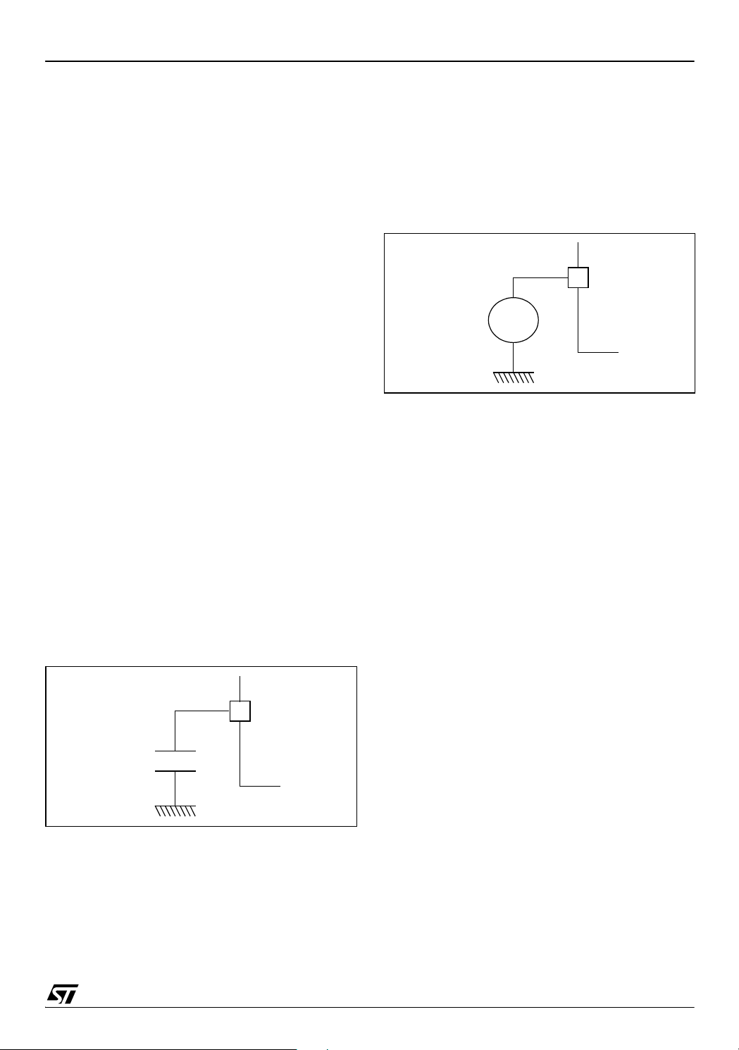
13 ELECTRICAL CHARACTERISTICS
13.1 PARAMETER CONDITIONS
ST7LITE1
Unless otherwise specified, all voltages are referred to V
SS
.
13.1.1 Minimum and Maximum values
Unless otherwise specified the minimum and maximum values are guaranteed in the worst conditions of ambient temperature, supply voltage and
frequencies by tests in production on 100% of the
devices with an ambient temperature at T
and T
max (given by the selected temperature
A=TA
=25°C
A
range).
Data based on characterization results, design
simulation and/or technology characteristics are
indicated in the table footnotes and are not tested
in production. Based on characterization, the minimum and maximum values refer to sample tests
and represent the mean value plus or minus three
times the standard deviation (mean±3Σ).
13.1.2 Typical values
Unless otherwise specified, typical data are based
=25°C, VDD=5V (for the 4.5V≤VDD≤5.5V
on T
A
voltage range) and V
=3.3V (for the 3V≤VDD≤4V
DD
voltage range). They are given only as design
guidelines and are not tested.
13.1.3 Typical curves
Unless otherwise specified, all typical curves are
given only as design guidelines and are not tested.
13.1.4 Loading capacitor
The loading conditions used for pin parameter
measurement are shown in Figure 49.
13.1.5 Pin input voltage
The input voltage measurement on a pin of the device is described in Figure 50.
Figure 50. Pin input voltage
ST7 PIN
V
IN
Figure 49. Pin loading conditions
C
L
ST7 PIN
91/131
1
Page 92

ST7LITE1
13.2 ABSOLUTE MAXIMUM RATINGS
Stresses above those listed as “absolute maximum ratings” may cause permanent damage to
the device. This is a stress rating only and functional operation of the device under these condi-
13.2.1 Voltage Characteristics
Symbol Ratings Maximum value Unit
V
- V
DD
V
IN
V
ESD(HBM)
SS
Supply voltage 7.0
Input voltage on any pin
1) & 2)
Electrostatic discharge voltage (Human Body Model)
13.2.2 Current Characteristics
Symbol Ratings Maximum value Unit
I
VDD
I
VSS
Total current into VDD power lines (source)
Total current out of VSS ground lines (sink)
Output current sunk by any standard I/O and control pin 25
I
IO
Output current sunk by any high sink I/O pin 50
Output current source by any I/Os and control pin - 25
Injected current on RESET pin ± 5
I
INJ(PIN)
2) & 4)
Injected current on OSC1 and OSC2 pins ± 5
Injected current on PB0 and PB1 pins
Injected current on any other pin
ΣI
INJ(PIN)
2)
Total injected current (sum of all I/O and control pins)
13.2.3 Thermal Characteristics
tions is not implied. Exposure to maximum rating
conditions for extended periods may affect device
reliability.
VSS-0.3 to VDD+0.3
see section 13.7.3 on
page 104
3)
3)
5)
6)
6)
100
100
+5
± 5
± 20
V
V
mA
Symbol Ratings Value Unit
T
STG
T
J
Storage temperature range -65 to +150 °C
Maximum junction temperature (see Table 21, “THERMAL CHARACTERISTICS,” on
page 119)
Notes:
1. Directly connecting the I/O pins to V
tion occurs (for example, due to a corrupted program counter). To guarantee safe operation, this connection has to be
done through a pull-up or pull-down resistor (typical: 10kΩ for I/Os). Unused I/O pins must be tied in the same way to V
or VSS according to their reset configuration.
2. I
respected, the injection current must be limited externally to the I
must never be exceeded. This is implicitly insured if VIN maximum is respected. If VIN maximum cannot be
INJ(PIN)
while a negative injection is induced by VIN<VSS. For true open-drain pads, there is no positive injection current, and the
corresponding V
3. All power (V
4. Negative injection disturbs the analog performance of the device. In particular, it induces leakage currents throughout
maximum must always be respected
IN
) and ground (VSS) lines must always be connected to the external supply.
DD
DD
or V
could damage the device if an unexpected change of the I/O configura-
SS
value. A positive injection is induced by VIN>V
INJ(PIN)
DD
DD
the device including the analog inputs. To avoid undesirable effects on the analog functions, care must be taken:
- Analog input pins must have a negative injection less than 0.8 mA (assuming that the impedance of the analog voltage
is lower than the specified limits)
- Pure digital pins must have a negative injection less than 1.6mA. In addition, it is recommended to inject the current as
far as possible from the analog input pins.
5. No negative current injection allowed on PB0 and PB1 pins.
6. When several inputs are submitted to a current injection, the maximum ΣI
and negative injected currents (instantaneous values). These results are based on characterisation with ΣI
mum current injection on four I/O port pins of the device.
is the absolute sum of the positive
INJ(PIN)
INJ(PIN)
maxi-
92/131
1
Page 93
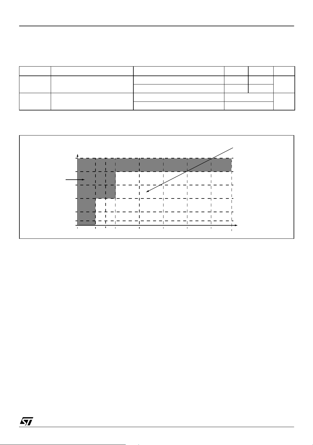
ST7LITE1
13.3 OPERATING CONDITIONS
13.3.1 General Operating Conditions: Suffix 6 Devices
T
= -40 to +85°C unless otherwise specified.
A
Symbol Parameter Conditions Min Max Unit
f
= 8 MHz. max., 2.4 5.5
V
DD
f
CLKIN
Supply voltage
External clock frequency on
CLKIN pin
OSC
= 16 MHz. max. 3.3 5.5
f
OSC
3.3V≤ V
2.4V≤V
≤5.5V up to 16
DD
<3.3V up to 8
DD
V
MHz
Figure 51. f
FUNCTIONALITY
NOT GUARANTEED
CLKIN
IN THIS AREA
Maximum Operating Frequency Versus V
f
[MHz]
CLKIN
16
8
4
1
0
2.0 2.4
2.7
3.3 3.5 4.0 4.5 5.0
Supply Voltage
DD
FUNCTIONALITY
GUARANTEED
IN THIS AREA
(UNLESS OTHERWISE
STATED IN THE
TABLES OF
PARAMETRIC DATA)
SUPPLY VOLTAGE [V]
5.5
93/131
1
Page 94
ST7LITE1
13.3.2 Operating Conditions with Low Voltage Detector (LVD)
T
= -40 to 85°C, unless otherwise specified
A
Symbol Parameter Conditions Min Typ Max Unit
1)
V
IT+
V
IT-
(LVD)
V
hys
Vt
POR
t
g(VDD)
I
DD(LVD
(LVD)
Reset release threshold
rise)
(V
DD
Reset generation threshold
fall)
(V
DD
LVD voltage threshold hysteresis V
VDD rise time rate
Filtered glitch delay on V
2)
DD
) LVD/AVD current consumption 220 µA
High Threshold
Med. Threshold
Low Threshold
High Threshold
Med. Threshold
Low Threshold
(LVD)
-V
IT-
(LVD)
IT+
Not detected by the LVD 150 ns
Note:
1. Not tested in production.
2. Not tested in production. The V
When the V
slope is outside these values, the LVD may not ensure a proper reset of the MCU.
DD
rise time rate condition is needed to insure a correct device power-on and LVD reset.
DD
13.3.3 Auxiliary Voltage Detector (AVD) Thresholds
T
= -40 to 85°C, unless otherwise specified
A
Symbol Parameter Conditions Min Typ Max Unit
V
V
V
∆V
IT+
IT-
hys
(AVD)
(AVD)
IT-
1=>0 AVDF flag toggle threshold
rise)
(V
DD
0=>1 AVDF flag toggle threshold
fall)
(V
DD
AVD voltage threshold hysteresis V
Voltage drop between AVD flag set
and LVD reset activation
Note:
1. Not tested in production.
High Threshold
Med. Threshold
Low Threshold
High Threshold
Med. Threshold
Low Threshold
IT+
V
DD
-V
(AVD)
IT-
(AVD)
fall 0.45 V
4.00
3.40
2.65
3.80
3.20
2.40
1)
4.25
1)
3.60
2.90
4.05
3.40
2.70
4.50
3.80
3.15
4.30
3.65
2.90
1)
1)
1)
200 mV
20 20000 µs/V
1)
4.40
3.90
3.20
4.30
3.70
2.90
4.70
1)
4.10
1)
3.40
4.60
3.90
3.20
5.00
4.30
3.60
4.90
4.10
3.40
1)
1)
1)
150 mV
V
V
13.3.4 Internal RC Oscillator and PLL
The ST7 internal clock can be supplied by an internal RC oscillator and PLL (selectable by option byte).
Symbol Parameter Conditions Min Typ Max Unit
V
DD(RC)
DD(x4PLL)
V
DD(x8PLL)
Internal RC Oscillator operating voltage 2.4 5.5
x4 PLL operating voltage 2.4 3.3
x8 PLL operating voltage 3.3 5.5
VV
PLL
input
t
STARTUP
PLL Startup time 60
clock
(f
PLL
cycles
94/131
1
)
Page 95
ST7LITE1
OPERATING CONDITIONS (Cont’d)
The RC oscillator and PLL characteristics are temperature-dependent and are grouped in four tables.
13.3.4.1 Devices with ‘”6” order code suffix (tested for T
Symbol Parameter Conditions Min Typ Max Unit
f
RC
ACC
I
DD(RC)
t
su(RC)
f
PLL
t
LOCK
t
STAB
ACC
t
w(JIT)
JIT
PLL
I
DD(PLL)
Internal RC oscillator frequency
Accuracy of Internal RC
oscillator with
RC
RCCR=RCCR0
2)
RC oscillator current consumption
RC oscillator setup time TA=25°C,VDD=5V 10
x8 PLL input clock 1
PLL Lock time
5)
PLL Stabilization time
x8 PLL Accuracy
PLL
PLL jitter period fRC = 1MHz 8
PLL jitter (∆f
CPU/fCPU
PLL current consumption TA=25°C 600
RCCR = FF (reset value), T
RCCR = RCCR0
2 )
,TA=25°C,VDD=5V 1000
TA=25°C,VDD=4.5 to 5.5V -1 +1%
T
=-40 to +85°C,VDD=5V -5 +2 %
A
=0 to +85°C,VDD=4.5 to 5.5V -2
T
A
=25°C,VDD=5V 970
T
A
5)
= 1MHz@TA=25°C,VDD=4.5 to 5.5V 0.1
f
RC
f
= 1MHz@TA=-40 to +85°C,VDD=5V 0.1
RC
)1
= -40 to +85°C) @ VDD = 4.5 to 5.5V
A
=25°C,VDD=5V 760
A
1)
+2
1)
1)
2ms
4ms
4)
4)
3)
3)
1)
kHz
1)
%
µA
2)
µs
MHz
%
%
kHz
%
µA
Notes:
1. Data based on characterization results, not tested in production
2. RCCR0 is a factory-calibrated setting for 1000kHz with ±0.2 accuracy @ T
CILLATOR ADJUSTMENT” on page 23
3. Guaranteed by design.
4. Averaged over a 4ms period. After the LOCKED bit is set, a period of t
5. After the LOCKED bit is set ACC
is max. 10% until t
PLL
has elapsed. See Figure 11 on page 24.
STAB
STAB
=25°C, VDD=5V. See “INTERNAL RC OS-
A
is required to reach ACC
accuracy.
PLL
95/131
1
Page 96

ST7LITE1
OPERATING CONDITIONS (Cont’d)
13.3.4.2 Devices with ‘”6” order code suffix (tested for T
Symbol Parameter Conditions Min Typ Max Unit
f
RC
ACC
I
DD(RC)
t
su(RC)
f
PLL
t
LOCK
t
STAB
ACC
t
w(JIT)
JIT
PLL
I
DD(PLL)
Internal RC oscillator frequency
Accuracy of Internal RC
oscillator when calibrated
RC
with RCCR=RCCR1
RC oscillator current consumption
RC oscillator setup time TA=25°C,VDD=3V 10
x4 PLL input clock 0.7
PLL Lock time
5)
PLL Stabilization time
x4 PLL Accuracy
PLL
PLL jitter period fRC = 1MHz 8
PLL jitter (∆f
CPU/fCPU
PLL current consumption TA=25°C 190
RCCR = FF (reset value), T
RCCR=RCCR1
2)
,TA=25°C,VDD= 3V 700
TA=25°C,VDD=3V -2 +2 %
T
=25°C,VDD=2.7 to 3.3V -25 +25 %
1)2)
A
T
=-40 to +85°C,VDD=3V -15 15 %
A
=25°C,VDD=3V 700
T
A
5)
= 1MHz@TA=25°C,VDD=2.7 to 3.3V 0.1
f
RC
= 1MHz@TA=40 to +85°C,VDD= 3V 0.1
f
RC
)1
= -40 to +85°C) @ VDD = 2.7 to 3.3V
A
=25°C, VDD= 3.0V 560
A
1)
1)
2ms
4ms
4)
4)
3)
3)
1)
2)
kHz
µA
µs
MHz
%
%
kHz
%
µA
Notes:
1. Data based on characterization results, not tested in production
2. RCCR1 is a factory-calibrated setting for 700MHz with ±0.2 accuracy @ T
CILLATOR ADJUSTMENT” on page 23.
3. Guaranteed by design.
4. Averaged over a 4ms period. After the LOCKED bit is set, a period of t
5. After the LOCKED bit is set ACC
is max. 10% until t
PLL
has elapsed. See Figure 11 on page 24.
STAB
STAB
=25°C, VDD=3V. See “INTERNAL RC OS-
A
is required to reach ACC
accuracy
PLL
96/131
1
Page 97

OPERATING CONDITIONS (Cont’d)
)
ST7LITE1
Figure 52. RC Osc Freq vs V
(Calibrated with RCCR1: 3V @ 25°C)
@ TA=25°C
DD
1.00
0.90
0.80
0.70
0.60
Output Freq (MHz
0.50
2.4 2.6 2.8 3 3.2 3.4 3.6 3.8 4
VDD (V)
Figure 54. Typical RC oscillator Accuracy vs
temperature @ V
(Calibrated with RCCR0: 5V @ 25°C
2
1
0
-1
RC Accuracy
-2
-3
-4
(
)
*
-5
-45 025 85
) tested in production
(
*
=5V
DD
Temperature (°C)
)
(
*
(*)
125
Figure 53. RC Osc Freq vs V
(Calibrated with RCCR0: 5V@ 25°C)
1.10
1.00
0.90
0.80
0.70
0.60
0.50
0.40
0.30
Output Freq. (MHz)
0.20
0.10
0.00
2.533.544.555.56
Vdd (V)
Figure 55. RC Osc Freq vs V
1.80
1.60
1.40
1.20
1.00
0.80
0.60
Output Freq. (MHz)
0.40
0.20
0.00
2.4 2.7 3 3.3 3.75 4 4.5 5 5.5 6
Vdd (V)
DD
and RCCR Value
DD
-45°
0°
25°
90°
105°
130°
rccr=00h
rccr=64h
rccr=80h
rccr=C0h
rccr=FFh
97/131
1
Page 98

ST7LITE1
OPERATING CONDITIONS (Cont’d)
Figure 56. PLL ∆f
∆f
Max
0
Min
CPU/fCPU
CPU/fCPU
versus time
Figure 57. PLLx4 Output vs CLKIN frequency
7.00
6.00
5.00
4.00
3.00
Output Frequency (MHz)
2.00
1.00
11.522.53
Ext ernal Input Cloc k Frequency (MHz)
3.3
3
2.7
t
w(JIT)
t
w(JIT)
Figure 58. PLLx8 Output vs CLKIN frequency
11.00
9.00
7.00
5.00
3.00
Output Frequency (MHz)
1.00
0.85 0.9 1 1.5 2 2.5
External Input Clock Frequency (MHz)
t
5.5
5
4.5
4
Note: f
OSC
= f
CLKIN
/2*PLL4
13.3.4.3 32MHz PLL
= -40 to 85°C, unless otherwise specified
T
A
Symbol Parameter Min Typ Max Unit
V
DD
f
PLL32
f
INPUT
Voltage
Frequency
Input Frequency
Note 1: 32 MHz is guaranteed within this voltage range.
98/131
1)
1)
Note: f
OSC
= f
CLKIN
/2*PLL8
4.5 5 5.5 V
32 MHz
7
89MHz
1
Page 99

13.4 SUPPLY CURRENT CHARACTERISTICS
ST7LITE1
The following current consumption specified for
the ST7 functional operating modes over temperature range does not take into account the clock
vice consumption, the two current values must be
added (except for HALT mode for which the clock
is stopped).
source current consumption. To get the total de-
13.4.1 Supply Current
= -40 to +85°C unless otherwise specified, V
T
A
Symbol Parameter Conditions Typ Max Unit
Supply current in RUN mode
Supply current in WAIT mode
I
DD
Supply current in SLOW mode f
Supply current in SLOW WAIT mode f
Supply current in HALT mode
Supply current in AWUFH mode
5)
6)7)
Notes:
1. CPU running with memory access, all I/O pins in input mode with a static value at V
in reset state; clock input (CLKIN) driven by external square wave, LVD disabled.
2. All I/O pins in input mode with a static value at V
driven by external square wave, LVD disabled.
3. SLOW mode selected with f
(no load), all peripherals in reset state; clock input (CLKIN) driven by external square wave, LVD disabled.
V
SS
4. SLOW-WAIT mode selected with f
or VSS (no load), all peripherals in reset state; clock input (CLKIN) driven by external square wave, LVD disabled.
V
DD
based on f
CPU
based on f
CPU
OSC
5. All I/O pins in output mode with a static value at V
tested in production at VDD max and f
CPU
max.
6. All I/O pins in input mode with a static value at V
max.
7. This consumption refers to the Halt period only and not the associated run period which is software dependent.
=5.5V
DD
External Clock, f
Internal RC, f
f
CPU
=8MHz
1)
External Clock, f
Internal RC, f
f
CPU
CPU
CPU
=8MHz
=250kHz
=250kHz
2)
=1MHz
CPU
=1MHz 2.2
CPU
=1MHz
CPU
=1MHz 1.8
CPU
3)
4)
-40°C≤TA≤+85°C
= +125°C
A
TA= +25°C
or VSS (no load), all peripherals in reset state; clock input (CLKIN)
DD
1)
1
7.5 12
2)
0.8
mA
3.7 6
1.6 2.5
1.6 2.5
110
15 50
µAT
20 30
or VSS (no load), all peripherals
DD
divided by 32. All I/O pins in input mode with a static value at VDD or
divided by 32. All I/O pins in input mode with a static value at
OSC
(no load), LVD disabled. Data based on characterization results,
SS
or VSS (no load). Data tested in production at VDD max. and f
DD
CPU
Figure 59. Typical IDD in RUN vs. f
9.0
8.0
7.0
6.0
5.0
4.0
Idd (mA)
3.0
2.0
1.0
0.0
2.02.53.03.54.04.55.05.56.0
8Mhz
4Mhz
1Mhz
Vdd (V)
CPU
Figure 60. Typical IDD in SLOW vs. f
1.6
1.4
1.2
1.0
0.8
0.6
Idd (mA)
0.4
0.2
0.0
250Khz
125Khz
62.5Hz
2 2.5 3 3.5 4 4.5 5 5.5 6
Vdd (V)
CPU
99/131
1
Page 100

ST7LITE1
SUPPLY CURRENT CHARACTERISITCS (Cont’d)
Figure 61. Typical I
4.5
4.0
3.5
3.0
2.5
2.0
Idd (mA)
1.5
1.0
0.5
0.0
8Mhz
4Mhz
1MHz
2.0 2.5 3.0 3.5 4.0 4.5 5.0 5.5 6.0
in WAIT vs. f
DD
Vdd (V)
CPU
Figure 62. Typical IDD in SLOW-WAIT vs. f
1.4
1.2
1.0
0.8
0.6
Idd (mA)
0.4
0.2
0.0
250KHz
125KHz
62.5Khz
TBD
2.0 2.5 3.0 3.5 4.0 4.5 5.0 5.5 6.0
Vdd (V)
CPU
Figure 63. Typical IDD in AWUFH mode
at T
=25°C
A
0.035
0.030
0.025
0.020
0.015
Idd(mA)
0.010
0.005
0.000
Figure 64. Typical I
at V
= 5V and f
DD
8.0
7.0
6.0
5.0
Idd (mA)
4.0
fawu_rc ~125 KHz
2.0 2.5 3.0 3.5 4.0 4.5 5.0 5.5 6.0
Vdd(V)
vs. Temperature
DD
= 8MHz
CPU
25°
-45°
90°
130°
3.0
2.0
2.4 2.8 3.2 3.6 4 4.4 4.8 5.2 5.6
Vdd (V)
13.4.2 On-chip peripherals
Symbol Parameter Conditions Typ Unit
f
=4MHz VDD=3.0V 300
I
DD(AT)
I
DD(SPI)
I
DD(ADC)
12-bit Auto-Reload Timer supply current
SPI supply current
2)
ADC supply current when converting
1)
3)
1. Data based on a differential IDD measurement between reset configuration (timer stopped) and a timer running in PWM
mode at f
2. Data based on a differential I
tion (data sent equal to 55h).
3. Data based on a differential I
cpu
=8MHz.
measurement between reset configuration and a permanent SPI master communica-
DD
measurement between reset configuration and continuous A/D conversions with am-
DD
plifier off.
CPU
f
=8MHz VDD=5.0V 1000
CPU
f
=4MHz VDD=3.0V 50
CPU
f
=8MHz VDD=5.0V 300
CPU
=3.0V 250
V
f
ADC
=4MHz
DD
V
=5.0V 1100
DD
µA
100/131
1
 Loading...