

STMicroelectronics ST755 Technical data

ADJUSTABLE INVERTING NEGATIVE OUTPUT
CURRENT MODE PWM REGULATORS
■ 2.7V TO 11V INPUT TO ADJUSTABLE
NEGATIVE OUTPUT CONVERSION
■ 1W GUARANTEED OUTPUT POWER
(V
>4.5V,T≤70°C)
I
■ 68% TYP. EFFICENCY AT 6V
■ VERY LOW QUIESCENT CURRENT:1.2mA
IN ON MODE, 10µA IN SH UT DOWN MODE
■ SOFT START
■ VERY LOW NOISE OUTPUT
■ 160KHz FIXED FREQUENCY OSCILLATOR
■ MIXED BIPOLAR-CMOS TECHNO LOG Y
DESCRIPTION
The ST755 is an adjustable inverting switch-mode
DC-DC regulator with internal Power MOSFET
that generators an adjustable negative output
from a voltage input of 2.7V to 11V , output current
guaranteed at 200mA (for V
>4.5V,VO=-5Vand
I
ST755
DIP-8 SO-8
T
= 0°C to 70°C) and 275mA (typical value at T
A
=25°C,VO=-5V).
A logic controlled shut down pin that interfaces
directly with microprocessor reduces supply
current to only 10mA. Input to Output differential
voltage is limited to V
supply current is 1. 2mA.
+|VO|<12.7V. No load
I
A
SCHEMATIC DIAGRAM
1/10June 2003
ST755
ABSOLUTE MAXIMUM RATINGS
Symbol Parameter² Value Unit
V
V
SHDN
V
V
I
LX
P
TOT
T
T
Absolute Maximum Ratings are those values beyond which damage to the device may occur. Functional operation under these condition is
not implied.
Note 1: The input to output differential voltage is limited to V
THERMAL DATA
Symbol Parameter SO-8 DIP-8 Unit
R
thj-amb
(*) This value depends from thermal design of PCB on which the device is mounted.
DC Input Voltage to GND (Note1)
CC
-0.3 to 12 V
Shutdown Voltage, SS Voltage, CC Voltage -0.3 to (VCC+ 0.3)
Switch Voltage (LX to VCC)
LX
Feedback Voltage (VOto GND)
FB
Peak Switch Current
Continuous Power Dissipation at TA= 70°C (DIP-8)
(SO-8)
Operating Junction Temperature Range (C series) -40 to 185 °C
op
Storage Temperature Range
stg
+|VO|<12.7V
CC
Thermal Resistance Junction-ambient (*)
-12.5 to + 0.3 V
-11 to + 0.9 V
2A
725
470
-55 to +150 °C
160 100 °C/W
V
mW
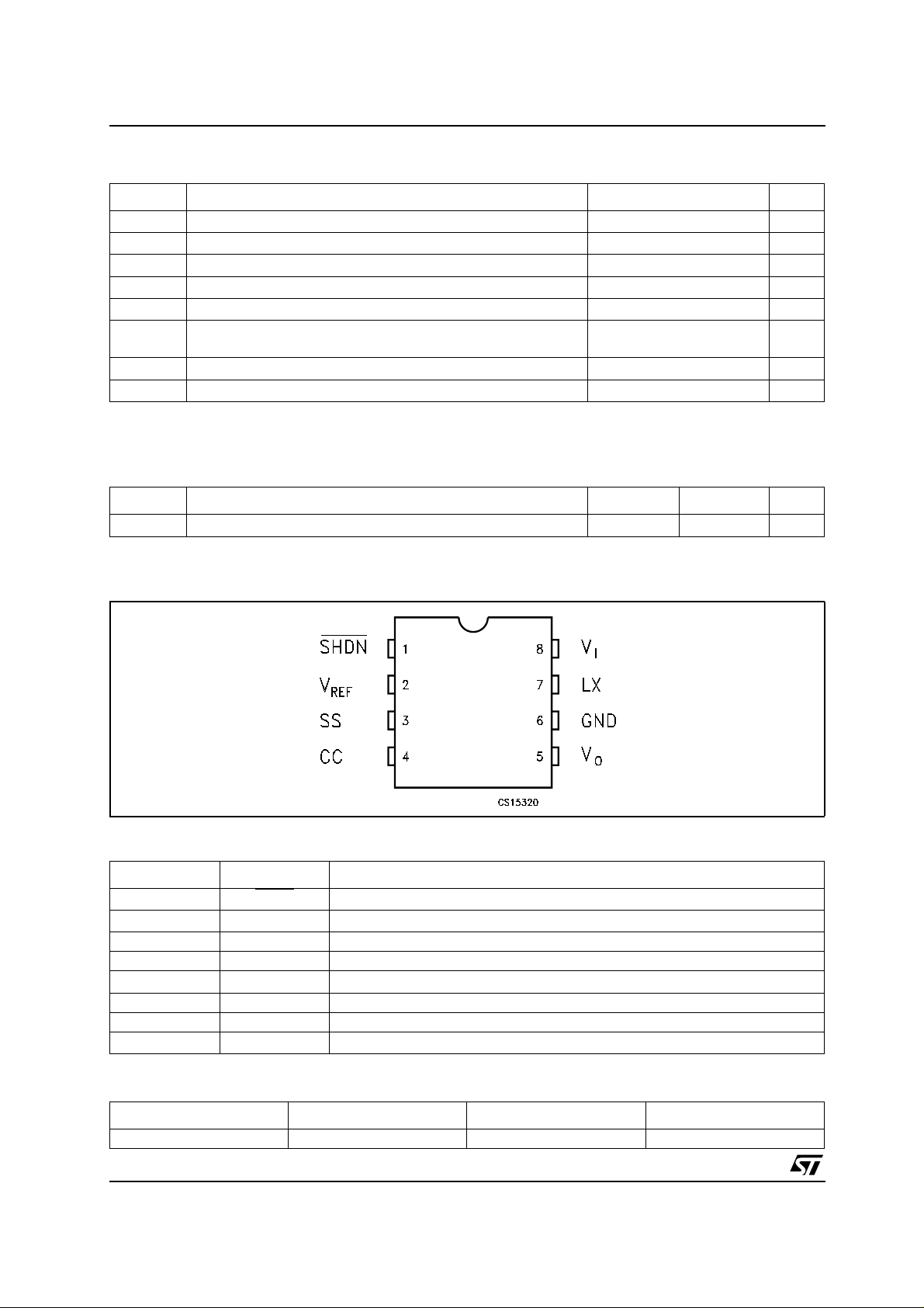
CONNECTION DIAGRAM (top view)
PIN DESCRIPTION
Pin N° Symbol Name and Function
1 SHDN
2V
REF
3 SS Soft Start
4 CC Compensation Input
5V
O
6 GND Ground
7 LX Switch Output
8V
CC
SHUT-DOWN control (VCC= ON, GND = Shutdown)
Reference Output Voltage: (1.25V)
Negative Output Voltage
Supply Voltage Input.
ORDERING CODES
TYPE DIP8 SO-8 SO-8 (T&R)
ST755 ST755CN ST755CD ST755CD-TR
2/10
ST755
ELECTRICAL CHARACTERISTICS (Refer to the test circuits , VCC=5V,VO= -5.25 to -4.75V,
I
=0mA,TA=T
LOAD
Symbol Parameter Test Conditions Min. Typ. Max. Unit
VIInput Voltage 4 11 V
Output Voltage VCC= 4.5 to 6.2V IO=0 to 200mA 4.75 5 5.25 V
V
O
Output Current VCC= 4.5 to 6.2V TA= 0 to 70°C 200 275 mA
I
O
I
SUPPLY
I
∆V
∆V
V
∆V
R
I
LEAK
f
Supply Current (Including
Switching Current)
Standby Current) No Load V
OFF
Short Circuit Current) 1.2 A
I
SC
Line Regulation VCC= 4 to 6.2V 0.1 %/V
O
Load Regulation IO= 0 to 200mA 0.003 %/mA
O
Reference Voltage TA= 25°C 1.18 1.25 1.32 V
REF
Reference Drift TA=T
REF
LX On Resistance 0.7 Ω
DSON
LX Leakage Current) VDS= 10V 1 µA
Shutdown Pin Current) 1 µA
I
SH
SHDN Input High Threshold 2 V
V
IH
SHDN Input Low Threshold 0.25 V
V
IL
Oscillator Frequency 160 KHz
OSC
η Power Efficiency I
CC Compensation Pin
Impedance
Do not overload or short the Output to Ground. If the above conditions are observed, the device may be damaged.
MIN
to T
, unless otherwise s pec ified. Typical value are referred at TA= 25°C)
MAX
= 4.5 to 6.2V TA= -40 to 85°C 175
V
CC
=4V VO= -5V 175
V
CC
V
= 2.7V VO= -5V 125
CC
No Load V
to T
MIN
=100mA 68 %
O
MAX
SHDN=VCC
=0V 10 100 µA
SHDN
1.2 3.5 mA
50 ppm/°C
7.5 KΩ
APPLICATION INFORMATION
The ST755 is a n IC developed for voltage conversion from an input volt age ranging from +2.4V to 11V to
a regulated adjustable negative output limite d by |V
| ≤ 12 .7V-VI. The circuit adopts a current-mode PWM
O
control scheme to achieve good efficiency, high stability and low noise performance. The figure in the first
page shown the detailed b lock diagram of the device.
ST755 is realized in a BCD technology in order to achieve high temperature stability, the best
REFERENCE precision, a very low quiescent current and jitter free operat ions. The f inal stage is built
around a 0.7Ω - 2 A P-Channel Power MOS. A f raction of the output curren t is splitted o ut for current
detection.Internal clock frequency is fixed to 160KHz. Error amplifier drives the PWM comparator in order
to keep 0V on the CC input. So R
V
)*R3(see fig 1). For R3can be choose any value between 2KΩ and 20KΩ. Soft-Start (SS) input is a
REF
and R4resistors are calculated by t he following formulae R4= (|VO|/
3
voltage dependent-output current limit (see figure 9, Switch Current Limit vs. SS Input V oltage). SS pin is
internally pulled to V
through a 1.2 MΩ resistor. Applying an appropriate capacitor at SS input is
REF
possible to obtain a s of t-start current imitation during power up. F orcing Soft -Start (SS) input to a lower
voltage through a resistive voltage driver (R
and R2), the maximum LX current limit can be lowered
1
according the diagram showed in figure 9. When SHDN input is l ow, the total current c ons umption is
reduced to 10µA.
APPLICATION CIRCUIT
To achieve the best performances from switch ing power supply topology, particular care to layout drawing
is needed, in order to minimize EMI and obtain low noise, jitter free operati on moreover, it ensures the full
device functionality. Layou t design proposed on demoboard (see pict ure 2) helps to lower the developing
3/10
 Loading...