

Page 1
8-BIT OTP/EPROM MCUs WITH A/D CONVERTER,
SAFE RESET, AUTO-RELOAD TIMER AND EEPROM
■ 3.0 to 6.0V Supply Operating Range
■ 8 MHz Maximum Clock Frequency
■ -40 to +125°C Operating Temperature Range
■ Run, Wait and Stop Modes
■ 5 Interrupt Vectors
■ Look-up Table capability in Program Memory
■ Data Storage in Program Memory:
User selectable size
■ Data RAM: 128 bytes
■ Data EEPROM: 64 bytes (none on ST 62T 5 2 C )
■ User Programmable Options
■ 9 I/O pins, fully programmable as:
– Input with pull-up resistor
– Input without pull-up resistor
– Input with interrupt generation
– Open-drain or push-pull output
– Analog Input
■ 5 I/O lines can sink up to 30mA to drive LEDs or
TRIACs directly
■ 8-bit Timer/Counter with 7-bit programmable
prescaler
■ 8-bit Auto-reload Timer with 7-bit programmable
prescaler (AR Timer)
■ Digital Watchdog
■ Oscillator Safe Guard
■ Low Voltage Detector for Safe Reset
■ 8-bit A/D Converter with 4 analog inputs
■ On-chip Clock oscillator can be driven by Quartz
Crystal Ceramic resonator or RC network
■ User configurable Power-on Reset
■ One external Non-Maskable Interrupt
■ ST626x-EMU2 Emulation and Development
System (connects to an MS-DOS PC via a
parallel port)
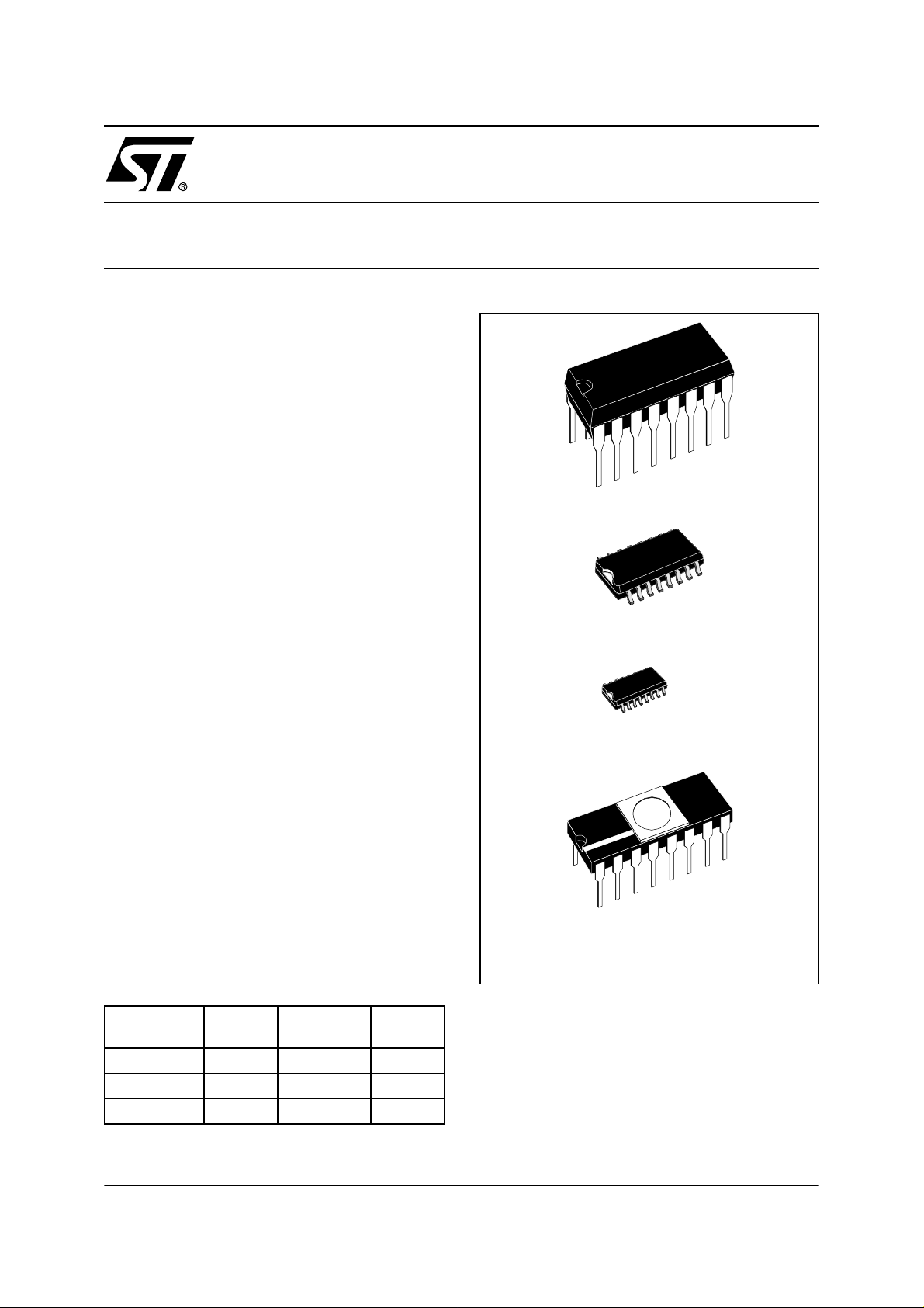
ST62T52C
ST62T62C/E62C
PDIP16
PSO16
SSOP16
CDIP16W
(See end of Datasheet for Ordering Information)
DEVICE SUMMARY
DEVICE
ST62T52C 1836 ST62T62C 1836 64
ST62E62C 1836 64
EPROM
(Bytes)
OTP
(Bytes)
EEPROM
Rev. 3.0
February 2002 1/78
Page 2

Table of Contents
Document
Page
ST62T52C
ST62T62C/E62C . . . . . . . . . . . . . . . . . . . . . . . . . . . . . . . . . . . . . 1
1 GENERAL DESCRIPTION . . . . . . . . . . . . . . . . . . . . . . . . . . . . . . . . . . . . . . . . . . . . . . . . . . . . . . 5
1.1 INTRODUCTION . . . . . . . . . . . . . . . . . . . . . . . . . . . . . . . . . . . . . . . . . . . . . . . . . . . . . . . . . 5
1.2 PIN DESCRIPTIONS . . . . . . . . . . . . . . . . . . . . . . . . . . . . . . . . . . . . . . . . . . . . . . . . . . . . . . 6
1.3 MEMORY MAP . . . . . . . . . . . . . . . . . . . . . . . . . . . . . . . . . . . . . . . . . . . . . . . . . . . . . . . . . . 7
1.3.1 Introduction . . . . . . . . . . . . . . . . . . . . . . . . . . . . . . . . . . . . . . . . . . . . . . . . . . . . . . . . 7
1.3.2 Program Space . . . . . . . . . . . . . . . . . . . . . . . . . . . . . . . . . . . . . . . . . . . . . . . . . . . . . 8
1.3.3 Data Space . . . . . . . . . . . . . . . . . . . . . . . . . . . . . . . . . . . . . . . . . . . . . . . . . . . . . . . . 9
1.3.4 Stack Space . . . . . . . . . . . . . . . . . . . . . . . . . . . . . . . . . . . . . . . . . . . . . . . . . . . . . . . . 9
1.3.5 Data Window Register (DWR) . . . . . . . . . . . . . . . . . . . . . . . . . . . . . . . . . . . . . . . . . 10
1.3.6 Data RAM/EEPROM Bank Register (DRBR) . . . . . . . . . . . . . . . . . . . . . . . . . . . . . . 11
1.3.7 EEPROM Description . . . . . . . . . . . . . . . . . . . . . . . . . . . . . . . . . . . . . . . . . . . . . . . 12
1.4 PROGRAMMING MODES . . . . . . . . . . . . . . . . . . . . . . . . . . . . . . . . . . . . . . . . . . . . . . . . . 14
1.4.1 Option Bytes . . . . . . . . . . . . . . . . . . . . . . . . . . . . . . . . . . . . . . . . . . . . . . . . . . . . . . 14
1.4.2 Program Memory . . . . . . . . . . . . . . . . . . . . . . . . . . . . . . . . . . . . . . . . . . . . . . . . . . . 14
1.4.3 . EEPROM Data Memory . . . . . . . . . . . . . . . . . . . . . . . . . . . . . . . . . . . . . . . . . . . . . 15
2 CENTRAL PROCESSING UNIT . . . . . . . . . . . . . . . . . . . . . . . . . . . . . . . . . . . . . . . . . . . . . . . . . 16
2.1 INTRODUCTION . . . . . . . . . . . . . . . . . . . . . . . . . . . . . . . . . . . . . . . . . . . . . . . . . . . . . . . . 16
2.2 CPU REGISTERS . . . . . . . . . . . . . . . . . . . . . . . . . . . . . . . . . . . . . . . . . . . . . . . . . . . . . . . 16
3 CLOCKS, RESET, INTERRUPTS AND POWER SAVING MODES . . . . . . . . . . . . . . . . . . . . . 18
3.1 CLOCK SYSTEM . . . . . . . . . . . . . . . . . . . . . . . . . . . . . . . . . . . . . . . . . . . . . . . . . . . . . . . . 18
3.1.1 Main Oscillator . . . . . . . . . . . . . . . . . . . . . . . . . . . . . . . . . . . . . . . . . . . . . . . . . . . . . 18
3.1.2 Low Frequenc y Au xiliar y Os c illa tor ( LFA O) . . . . . . . . . . . . . . . . . . . . . . . . . . . . . . . 19
3.1.3 Oscillator Safe Guard . . . . . . . . . . . . . . . . . . . . . . . . . . . . . . . . . . . . . . . . . . . . . . . . 19
3.2 RESETS . . . . . . . . . . . . . . . . . . . . . . . . . . . . . . . . . . . . . . . . . . . . . . . . . . . . . . . . . . . . . . . 22
3.2.1 RESET Input . . . . . . . . . . . . . . . . . . . . . . . . . . . . . . . . . . . . . . . . . . . . . . . . . . . . . . 22
3.2.2 Power-on Reset . . . . . . . . . . . . . . . . . . . . . . . . . . . . . . . . . . . . . . . . . . . . . . . . . . . . 22
3.2.3 Watchdog Reset . . . . . . . . . . . . . . . . . . . . . . . . . . . . . . . . . . . . . . . . . . . . . . . . . . . 23
3.2.4 LVD Reset . . . . . . . . . . . . . . . . . . . . . . . . . . . . . . . . . . . . . . . . . . . . . . . . . . . . . . . . 23
3.2.5 Application Notes . . . . . . . . . . . . . . . . . . . . . . . . . . . . . . . . . . . . . . . . . . . . . . . . . . . 23
3.2.6 MCU Initialization Sequence . . . . . . . . . . . . . . . . . . . . . . . . . . . . . . . . . . . . . . . . . . 24
3.3 DIGITAL WATCHDOG . . . . . . . . . . . . . . . . . . . . . . . . . . . . . . . . . . . . . . . . . . . . . . . . . . . . 26
3.3.1 Digital Watchdog Register (DWDR) . . . . . . . . . . . . . . . . . . . . . . . . . . . . . . . . . . . . . 28
3.3.2 Application Notes . . . . . . . . . . . . . . . . . . . . . . . . . . . . . . . . . . . . . . . . . . . . . . . . . . . 28
3.4 INTERRUPTS . . . . . . . . . . . . . . . . . . . . . . . . . . . . . . . . . . . . . . . . . . . . . . . . . . . . . . . . . . 30
3.4.1 Interrupt request . . . . . . . . . . . . . . . . . . . . . . . . . . . . . . . . . . . . . . . . . . . . . . . . . . . . 30
3.4.2 Interrupt Procedure . . . . . . . . . . . . . . . . . . . . . . . . . . . . . . . . . . . . . . . . . . . . . . . . . 31
3.4.3 Interrupt Option Register (IOR) . . . . . . . . . . . . . . . . . . . . . . . . . . . . . . . . . . . . . . . . 32
3.4.4 Interrupt Sources . . . . . . . . . . . . . . . . . . . . . . . . . . . . . . . . . . . . . . . . . . . . . . . . . . . 32
3.5 POWER SAVING MODES . . . . . . . . . . . . . . . . . . . . . . . . . . . . . . . . . . . . . . . . . . . . . . . . . 34
3.5.1 WAIT Mode . . . . . . . . . . . . . . . . . . . . . . . . . . . . . . . . . . . . . . . . . . . . . . . . . . . . . . . 34
3.5.2 STOP Mode . . . . . . . . . . . . . . . . . . . . . . . . . . . . . . . . . . . . . . . . . . . . . . . . . . . . . . . 34
3.5.3 Exit from WAIT and STOP Modes . . . . . . . . . . . . . . . . . . . . . . . . . . . . . . . . . . . . . . 35
78
2/78
Page 3

Table of Contents
4 ON-CHIP PERIPHERALS . . . . . . . . . . . . . . . . . . . . . . . . . . . . . . . . . . . . . . . . . . . . . . . . . . . . . . 36
4.1 I/O PORTS . . . . . . . . . . . . . . . . . . . . . . . . . . . . . . . . . . . . . . . . . . . . . . . . . . . . . . . . . . . . . 36
4.1.1 Operating Modes . . . . . . . . . . . . . . . . . . . . . . . . . . . . . . . . . . . . . . . . . . . . . . . . . . . 37
4.1.2 Safe I/O State Switching Sequence . . . . . . . . . . . . . . . . . . . . . . . . . . . . . . . . . . . . . 38
4.1.3 ARTimer alternate functions . . . . . . . . . . . . . . . . . . . . . . . . . . . . . . . . . . . . . . . . . . 40
4.2 TIMER . . . . . . . . . . . . . . . . . . . . . . . . . . . . . . . . . . . . . . . . . . . . . . . . . . . . . . . . . . . . . . . . 41
4.2.1 Timer Operation . . . . . . . . . . . . . . . . . . . . . . . . . . . . . . . . . . . . . . . . . . . . . . . . . . . . 42
4.2.2 Timer Interrupt . . . . . . . . . . . . . . . . . . . . . . . . . . . . . . . . . . . . . . . . . . . . . . . . . . . . . 42
4.2.3 Application Notes . . . . . . . . . . . . . . . . . . . . . . . . . . . . . . . . . . . . . . . . . . . . . . . . . . . 42
4.2.4 Timer Registers . . . . . . . . . . . . . . . . . . . . . . . . . . . . . . . . . . . . . . . . . . . . . . . . . . . . 43
4.3 AUTO-RELOAD TIMER . . . . . . . . . . . . . . . . . . . . . . . . . . . . . . . . . . . . . . . . . . . . . . . . . . . 44
4.3.1 AR Timer Description . . . . . . . . . . . . . . . . . . . . . . . . . . . . . . . . . . . . . . . . . . . . . . . . 44
4.3.2 Timer Operating Modes . . . . . . . . . . . . . . . . . . . . . . . . . . . . . . . . . . . . . . . . . . . . . . 44
4.3.3 AR Timer Registers . . . . . . . . . . . . . . . . . . . . . . . . . . . . . . . . . . . . . . . . . . . . . . . . . 48
4.4 A/D CONVERTER (ADC) . . . . . . . . . . . . . . . . . . . . . . . . . . . . . . . . . . . . . . . . . . . . . . . . . 50
4.4.1 Application Notes . . . . . . . . . . . . . . . . . . . . . . . . . . . . . . . . . . . . . . . . . . . . . . . . . . . 50
5 SOFTWARE . . . . . . . . . . . . . . . . . . . . . . . . . . . . . . . . . . . . . . . . . . . . . . . . . . . . . . . . . . . . . . . . 52
5.1 ST6 ARCHITECTURE . . . . . . . . . . . . . . . . . . . . . . . . . . . . . . . . . . . . . . . . . . . . . . . . . . . . 52
5.2 ADDRESSING MODES . . . . . . . . . . . . . . . . . . . . . . . . . . . . . . . . . . . . . . . . . . . . . . . . . . . 52
5.3 INSTRUCTION SET . . . . . . . . . . . . . . . . . . . . . . . . . . . . . . . . . . . . . . . . . . . . . . . . . . . . . . 53
6 ELECTRICAL CHARACTERISTICS . . . . . . . . . . . . . . . . . . . . . . . . . . . . . . . . . . . . . . . . . . . . . . 58
6.1 ABSOLUTE MAXIMUM RATINGS . . . . . . . . . . . . . . . . . . . . . . . . . . . . . . . . . . . . . . . . . . . 58
6.2 RECOMMENDED OPERATING CONDITIONS . . . . . . . . . . . . . . . . . . . . . . . . . . . . . . . . . 59
6.3 DC ELECTRICAL CHARACTERISTICS . . . . . . . . . . . . . . . . . . . . . . . . . . . . . . . . . . . . . . 60
6.4 AC ELECTRICAL CHARACTERISTICS . . . . . . . . . . . . . . . . . . . . . . . . . . . . . . . . . . . . . . 61
6.5 A/D CONVERTER CHARACTERISTICS . . . . . . . . . . . . . . . . . . . . . . . . . . . . . . . . . . . . . . 62
6.6 TIMER CHARACTERISTICS . . . . . . . . . . . . . . . . . . . . . . . . . . . . . . . . . . . . . . . . . . . . . . . 62
6.7 SPI CHARACTERISTICS . . . . . . . . . . . . . . . . . . . . . . . . . . . . . . . . . . . . . . . . . . . . . . . . . 62
6.8 ARTIMER ELECTRICAL CHARACTERISTICS . . . . . . . . . . . . . . . . . . . . . . . . . . . . . . . . . 62
7 GENERAL INFORMATION . . . . . . . . . . . . . . . . . . . . . . . . . . . . . . . . . . . . . . . . . . . . . . . . . . . . . 68
7.1 PACKAGE MECHANICAL DATA . . . . . . . . . . . . . . . . . . . . . . . . . . . . . . . . . . . . . . . . . . . . 68
7.2 ORDERING INFORMATION . . . . . . . . . . . . . . . . . . . . . . . . . . . . . . . . . . . . . . . . . . . . . . . 70
Document
Page
ST62P52C
ST62P62C . . . . . . . . . . . . . . . . . . . . . . . . . . . . . . . . . . . . . . . . . 71
1 GENERAL DESCRIPTION . . . . . . . . . . . . . . . . . . . . . . . . . . . . . . . . . . . . . . . . . . . . . . . . . . . . . . 72
1.1 INTRODUCTION . . . . . . . . . . . . . . . . . . . . . . . . . . . . . . . . . . . . . . . . . . . . . . . . . . . . . . . . . 72
1.2 ORDERING INFORMATION . . . . . . . . . . . . . . . . . . . . . . . . . . . . . . . . . . . . . . . . . . . . . . . . 72
1.2.1 Transfer of Customer Code . . . . . . . . . . . . . . . . . . . . . . . . . . . . . . . . . . . . . . . . . . . 72
1.2.2 Listing Generation and Verification . . . . . . . . . . . . . . . . . . . . . . . . . . . . . . . . . . . . . 72
3/78
Page 4

Table of Contents
Document
Page
ST6252C
ST6262 B . . . . . . . . . . . . . . . . . . . . . . . . . . . . . . . . . . . . . . . . . . . 73
1 GENERAL DESCRIPTION . . . . . . . . . . . . . . . . . . . . . . . . . . . . . . . . . . . . . . . . . . . . . . . . . . . . . . 74
1.1 INTRODUCTION . . . . . . . . . . . . . . . . . . . . . . . . . . . . . . . . . . . . . . . . . . . . . . . . . . . . . . . . . 74
1.2 ROM READOUT PROTECTION . . . . . . . . . . . . . . . . . . . . . . . . . . . . . . . . . . . . . . . . . . . . . 74
1.3 ORDERING INFORMATION . . . . . . . . . . . . . . . . . . . . . . . . . . . . . . . . . . . . . . . . . . . . . . . . 75
1.3.1 Transfer of Customer Code . . . . . . . . . . . . . . . . . . . . . . . . . . . . . . . . . . . . . . . . . . . 75
1.3.2 Listing Generation and Verification . . . . . . . . . . . . . . . . . . . . . . . . . . . . . . . . . . . . . 75
2 SUMMARY OF CHANGES . . . . . . . . . . . . . . . . . . . . . . . . . . . . . . . . . . . . . . . . . . . . . . . . . . . . . 77
4/78
78
Page 5
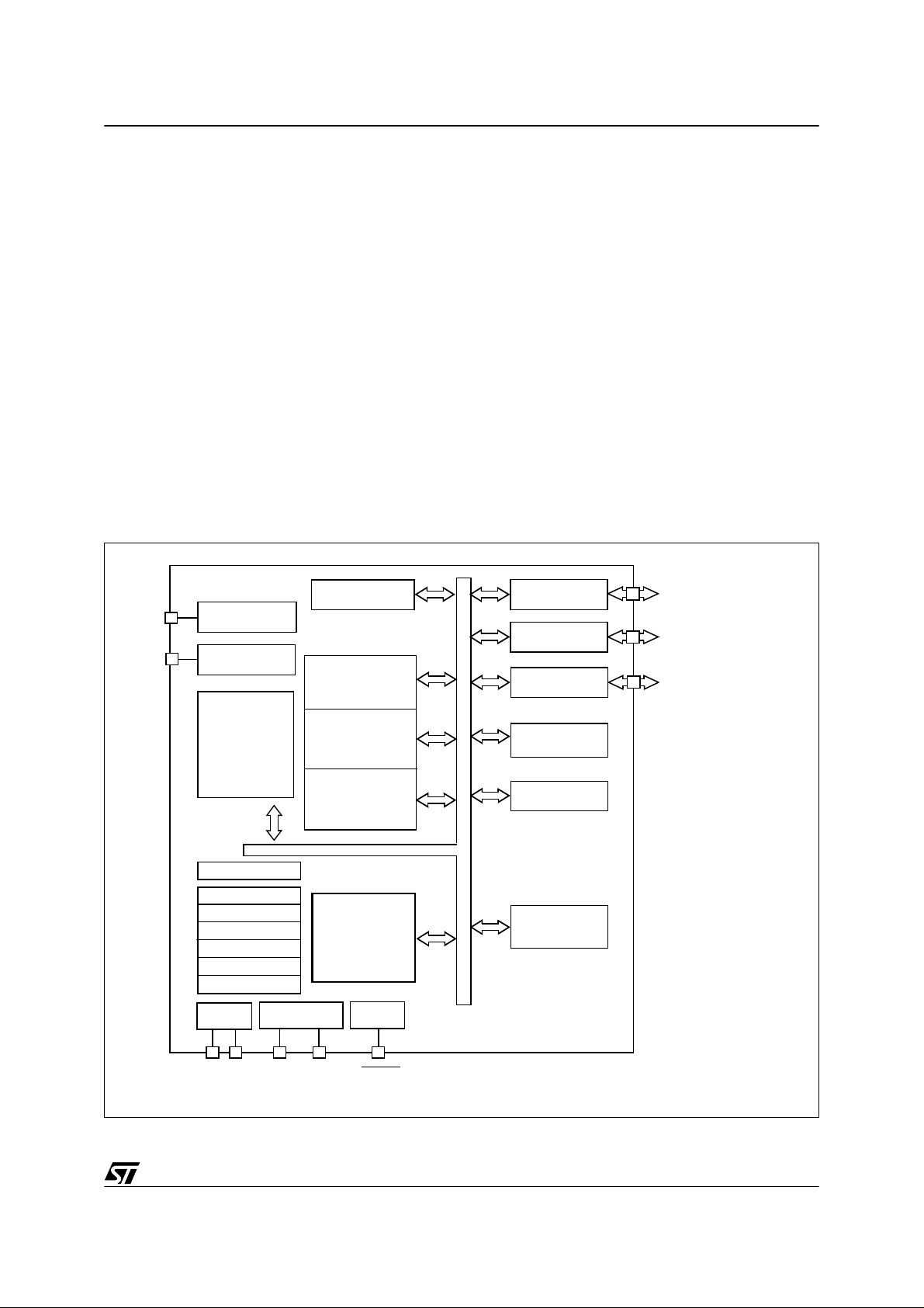
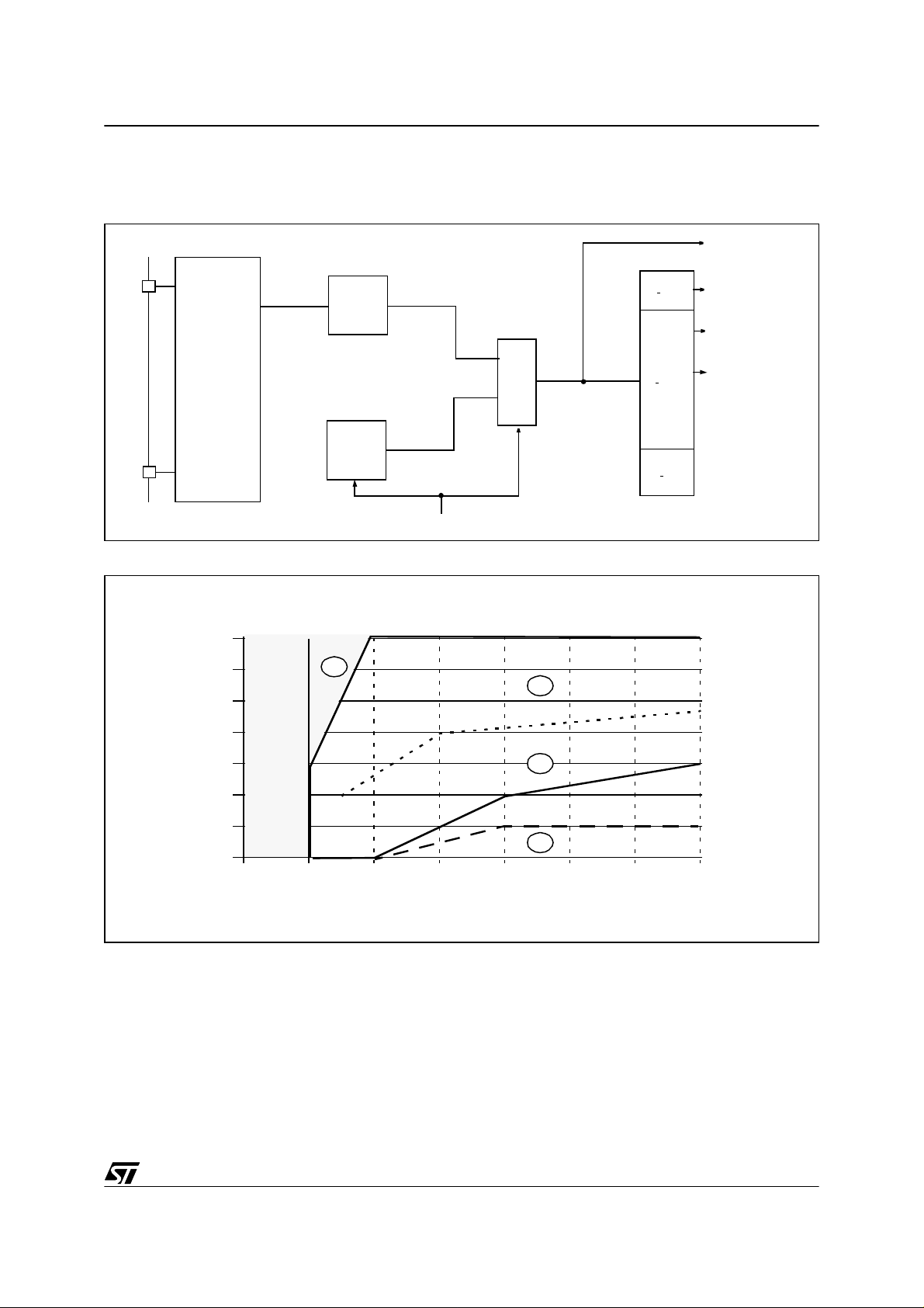
1 GENERAL DESCRIPTIO N
1.1 INTRODUCTION
ST62T52C ST62T62C/E62C
The ST62T52C and ST62T62C devices is low cost
members of the ST62xx 8-bit HCMOS family of microcontrollers, which is targeted at lo w t o med ium
complexity applications. All ST62xx devices are
based on a building block approach: a common
core is surrounded by a number of on-chip peripherals.
The ST62E62C is the erasable EPROM version of
the ST62T62C device, whi ch may be used to em ulate the ST62T52C and ST62T62C devices as
well as the ST6252C and ST6262B ROM devices.
OTP and EPROM devices are functional ly identical. The ROM based versions offer the same functionality selecting as ROM options the options de-
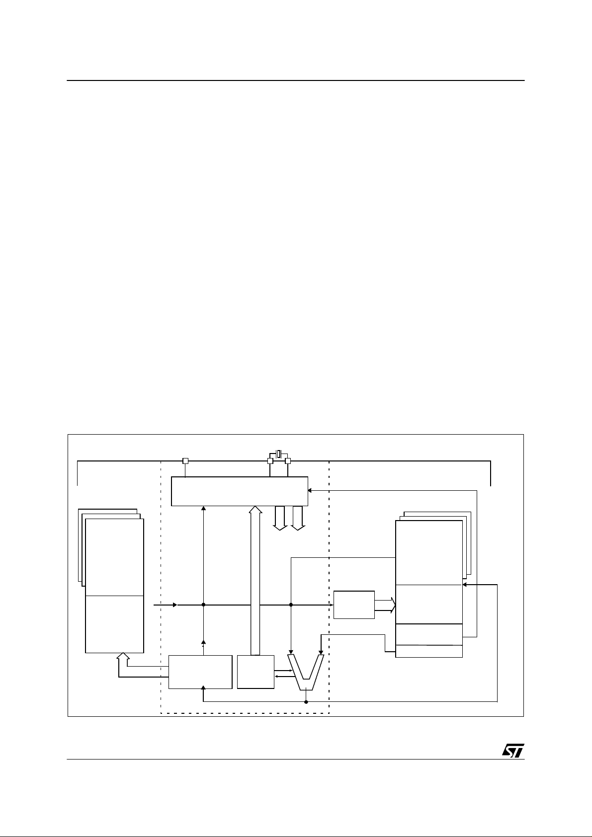
Figure 1. Block Diagram
8-BIT
TEST/V
PP
NMI INTER RUPT
TEST
PROGRAM
MEMORY
1836 bytes OTP
(ST62T52C, T62C)
1836 bytes EPROM
(ST62E62C)
A/D CONVERTER
DATA ROM
USER
SELECTABLE
DATA RAM
128 Bytes
DATA EEPROM
64 Bytes
(ST62T62C/E62C)
fined in the programmable option byte of the
OTP/EPROM versions.
OTP devices offer all the advant ages of user programmability at low cost, which make them the
ideal choice in a wide range of applications where
frequent code chang es, mu ltiple code vers ions or
last minute programmability are required.
These compact low -cost devices feature a Timer
comprising an 8-bit counter and a 7-bit programmable prescaler, an 8-bit Auto-Reload Timer,
EEPRO M data capa bility (exce pt ST62T52C ), an
8-bit A/D Converter with 4 analog inputs and a Digital Watchdog timer, making them well suited for a
wide range of automotive, appliance and industrial
applications.
PORT A
PORT B
PORT C PC2..PC3 / Ain
AUTORELOAD
TIMER
TIMER
PA4..PA5 / Ain
PB0, PB2..PB3 / 30 mA Sink
PB6 / ARTimin / 20 mA Sink
PB7 / ARTimout / 20 mA Sink
PC
STACK LEVEL 1
STACK LEVEL 2
STACK LEVEL 3
STACK LEVEL 4
STACK LEVEL 5
STACK LEVEL 6
POWER
SUPPLY
V
DDVSS
OSCILLATOR
OSCin OSCout RESET
8 BIT CORE
RESET
DIGITAL
WATCHDOG
5/78
Page 6

ST62T52C ST62T62C/E62C
1.2 PIN DESCRI PTIONS
V
and VSS. Power is suppl ied to the MCU vi a
DD
these two pins. V
V
is the ground connection.
SS
is the power conn ection and
DD
OSCin and OSCout. These pins are internally
connected to the on-chip oscillator circuit. A quartz
crystal, a ceramic resonator or an external clock
signal can be connected between these two pins.
The OSCin pin is the input pin, the OSCout pin is
the output pin.
RESET. The active-low RESET
pin is used to re-
start the microcontroller.
TEST/V
PP. The TEST must be held at V
for nor-
SS
mal operation. If TEST pin is connected to a
+12.5V level during the reset phase, the
EPROM/OTP programming Mode is entered.
NMI. The NMI pin provides the capability for asynchronous interruption, by applying an external non
maskable interrupt to the MCU. The NM I input is
falling edge sensitive. It is provided with an on-chip
pullup resistor (if option has been e nabled), and
Schmitt trigger characteristics.
PA4-PA5. Th es e 2 lines are orga nized as one I /O
port (A). Each line may be configu red under software control as inputs with or without internal pullup resistors, interrupt generating inputs with pullup resistors, open-drain or push-pull outputs, analog inputs for the A/D converter.
PB0, PB2-PB3, PB6-PB7. These 5 lines are organized as one I/O port (B). Each line may be configured under software control as inputs with or
without internal pull-up resistors, interrupt generating inputs with pull-up resistors, open-drain or
push-pull outputs. PB6/ARTIMin and PB7/ARTI-
Mout are either Port B I/O bits or the Input and
Output pins of the ARTimer.
Reset state of PB2-PB3 pins can be defined by option either with pull-up or high impedance.
PB0, PB2-PB3, PB6 -PB7 sca n also sink 30mA for
direct LED driving.
PC2-PC3. These 2 lines are organized as one I/O
port (C). Each line may be configured under software control as input with or without internal pullup resistor, interrupt generating in put with pull-up
resistor, analog input for the A/D converter, opendrain or push-pull output.
Figure 2. ST62T52C, E62C and T62C Pin
Configuration
PB0
V
/TEST
PP
PB2
PB3
ARTIMin/PB6
ARTIMout/PB7
V
DD
V
SS
1
2
3
4
5
6
7
8
16
15
14
13
12
10
11
9
PC2/Ain
PC3/Ain
NMI
RESET
OSCout
OSCin
PA5/Ain
PA4/Ain
6/78
Page 7

1.3 MEMORY MA P
ST62T52C ST62T62C/E62C
1.3.1 Introd uct i on
The MCU operates in three separate memory
spaces: Program space, Data space, and Stack
space. Operation in these three memory spaces is
described in the following paragraphs.
Figure 3. Mem ory Addressing D ia gram
PROGRAM SPACE
0000h
0-63
PROGRAM
MEMORY
Briefly, Program space contains user program
code in OTP and user vectors; Data space contains user data in RAM and in OTP, and Stack
space accommodat es six levels of stack for subroutine and interrupt service routine nesting.
DATA SPACE
000h
RAM / EEPROM
BANKING AREA
03Fh
040h
DATA READ-ONLY
WINDOW
RAM
07Fh
080h
081h
082h
083h
084h
MEMORY
X REGISTER
Y REGISTER
V REGISTER
W REGISTER
0FF0h
0FFFh
INTERRUPT &
RESET VECTORS
0C0h
0FFh
DATA READ-ONLY
MEMORY
WINDOW SELECT
DATA RAM
BANK SELECT
ACCUMULATOR
7/78
Page 8

ST62T52C ST62T62C/E62C
MEMORY MAP (Cont’d)
1.3.2 Program Space
Program Space comprises the instructions to b e
executed, the data required for immediate addressing mode instructions, the reserved factory
test area and the user v ectors. Program Space is
addressed via the 12-bit Program Counter register
(PC register).
1.3.2.1 Program Memory Protection
The Program Mem ory i n O TP or E P ROM devices
can be protected against external readout of memory by selecting the READOUT PROTECTION option in the option byte.
In the EPROM parts, READOUT PROTECTION
option can be disactivated only by U.V. erasure
that also results into the whole EPROM context
erasure.
Note: Once the Readout Protection is activated, it
is no longer possible, even for STMicroelectronics,
to gain access to the OTP contents. Returned
parts with a protection set can therefore not be accepted.
Figure 4. ST62T52C/T62C Program
Memory M a p
0000h
RESERVED
087Fh
0880h
USER
PROGRAM MEMORY
1836 BYTES
(OTP/EPROM)
*
0F9Fh
0FA0h
0FEFh
0FF0h
0FF7h
0FF8h
0FFBh
0FFCh
0FFDh
0FFEh
0FFFh
RESERVED
INTERRUPT VECTORS
RESERVED
NMI VECTOR
USER RESET VECTOR
*
(*) Reserved areas should be filled with 0FFh
8/78
Page 9
MEMORY MAP (Cont’d)
1.3.3 Data Space
Data Space accommodates all the data necessary
for processing the user program. This space comprises the RAM resource, the proc essor core an d
peripheral registers, as well as read-only data
such as constants and look-up tables in
OTP/EPROM.
1.3.3.1 Data ROM
All read-only data is physically stored in program
memory, which also accommodates the Program
Space. The program mem ory consequently contains the program code to be executed, as well as
the constants and look-up tables required by th e
application.
The Data Space locations in which the different
constants and look-up tables are addressed by the
processor core may be thought of as a 64-byte
window through which it is possible to acc ess the
read-only data stored in OTP/EPROM.
1.3.3.2 Data RAM/EEPROM
In ST62T52C, T62C and ST62E62C devices, the
data space includes 60 bytes of RAM, the accumulator (A), the i ndirect registers (X), (Y), t he short
direct registers (V), (W), the I/O port registers, the
peripheral data and control registers, the interrupt
option register and the Data ROM Window register
(DRW register).
Additional RAM and EEPROM pages can also be
addressed using banks of 64 bytes located between addresses 00h and 3Fh.
1.3.4 Stack Space
Stack space consists of six 12-bit registers which
are used to stack subroutine and interrupt return
addresses, as well as the current program counter
contents.
Table 1. Additional RAM / EEPROM Banks
Device RAM EEPROM
ST62T52C 1 x 64 bytes ST62T62C 1 x 64 bytes 1 x 64 bytes
ST62T52C ST62T62C/E62C
Table 2. ST62T52C, T62C and ST62E62C Data
Memory Space
RAM / EEPROM banks
DATA ROM WINDOW AREA
X REGISTER 080h
Y REGISTER 081h
V REGISTER 082h
W REGISTER 083h
DATA RAM 60 BYT ES
PORT A DATA REGISTER 0C0h
PORT B DATA REGISTER 0C1h
PORT C DAT A REGISTER 0C2h
RESERVED 0C3h
PORT A DIRECTION REGISTER 0C4h
PORT B DIRECTION REGISTER 0C5h
PORT C DIRECTION REGISTER 0C6h
RESERVED 0C7h
INTERRUPT OPTION REGISTER 0C8h*
DATA RO M WINDOW RE GIS T ER 0C9h*
RESERVED
PORT A OPTION REGISTER 0CCh
PORT B OPTION REGISTER 0CDh
PORT C OPTION REGISTER 0CEh
RESERVED 0CFh
A/D DATA REGISTER 0D0h
A/D CONTROL REGISTER 0D1h
TIMER PRESCALER REGISTE R 0D2h
TIMER COUNTER REGISTER 0D3h
TIMER S T A T US CONTRO L REGISTER 0D4h
AR TIMER MODE CONTROL REGI STER 0D5h
AR TIMER STATUS/CONTROL REGISTER1 0D6h
AR TIMER STATUS/CONTROL REGISTER2 0D7h
WATCHDOG REGISTER 0D8h
AR TIMER RELOAD/CAPTURE REGISTER 0D9h
AR TIMER COMPARE REGISTER 0DAh
AR TIMER LOAD REGISTER 0 DBh
RESERVED
DATA RAM/EEPROM REGISTER 0E8h*
RESERVED 0E9h
EEPROM CONTROL REGISTER 0EAh
RESERVED
ACCUMULATOR 0FFh
* WRITE ONLY REGISTE R
000h
03Fh
040h
07Fh
084h
0BFh
0CAh
0CBh
0DCh
0DDh
0DEh
0E7h
0EBh
0FEh
9/78
Page 10
ST62T52C ST62T62C/E62C
MEMORY MAP (Cont’d)
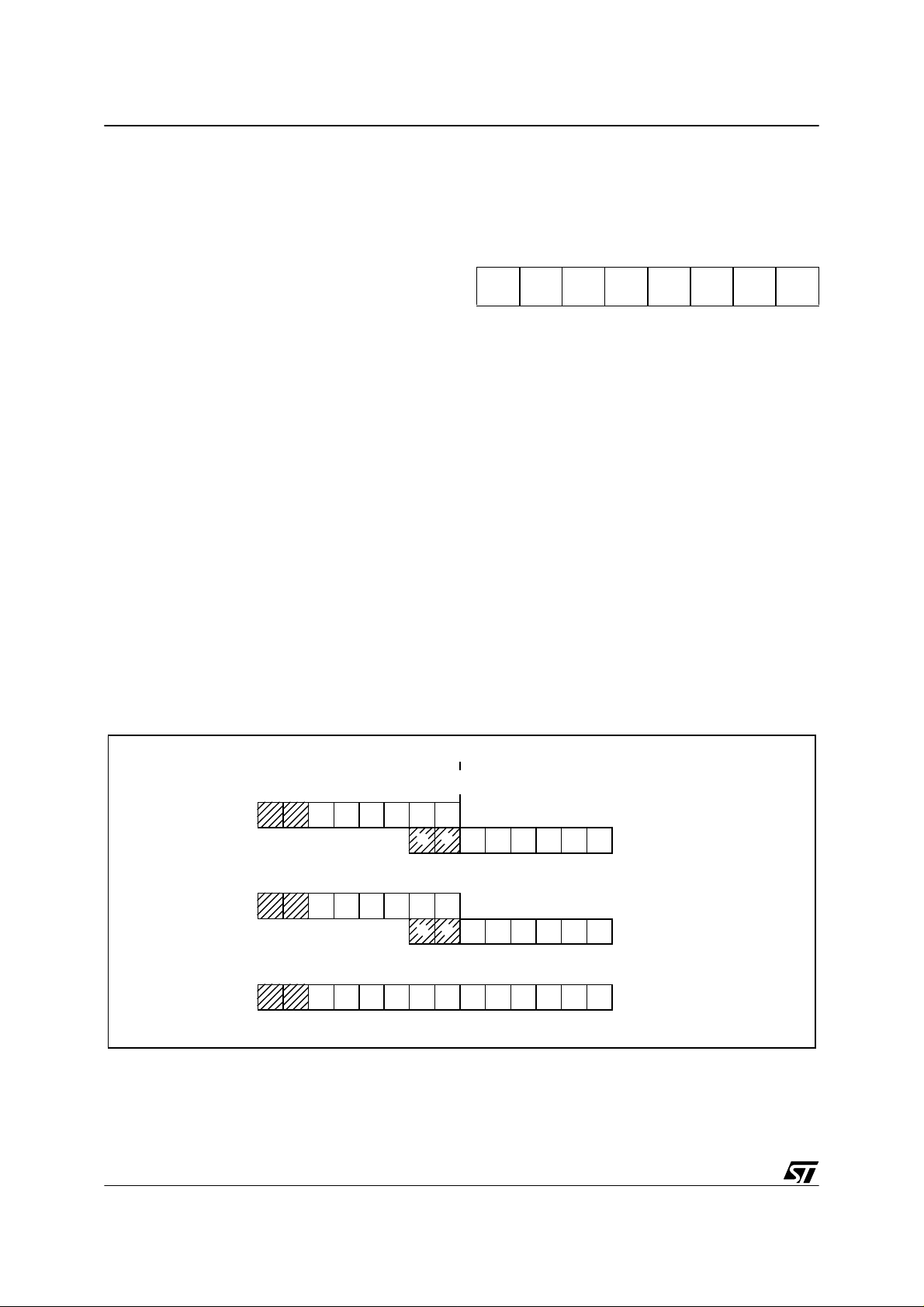
1.3.5 Data Window Register (DWR)
Data Wind ow R eg ist er (DWR)
The Data read-only memory window is located from
address 0040h to address 007Fh in Data space. It
allows direct reading of 64 consecutive bytes located anywhere in program memory, between address 0000h and 0FFFh (top memory address depends on the specific device). All the program
memory can therefore be used to store ei ther instructions or read-only data. Indeed, the window
can be moved i n steps of 64 byt es along the program memory by writing the appropriate code in the
Data Window Register (DWR).
The DWR can be addressed like any RAM location
in the Data Space, it is however a write-only register and therefore cannot be accessed using singlebit operations. This register is used to position the
64-byte read-only data window (from address 40 h
to address 7Fh of the Data space) in program
memory in 64-byte steps. The effective address of
the byte to be rea d as data in program me mory is
obtained by concatenating the 6 least significant
bits of the register address given in the instruction
(as least significant bits) and the content of the
DWR register (as most significant bits), as illustrated in Figure 5 below. For instance, when address-
ing location 0040h of the Data Space, with 0 loaded in the DWR register, the physical location addressed in program memory is 00h. The DWR register is not cleared on reset, therefore it must be
written to prior to the first access to the Data readonly memory window area.
Address: 0C9h — Write Only
70
- - DWR5 DWR4 DWR3 DWR2 DWR1 DWR0
Bits 6, 7 = Not used.
Bit 5-0 = DWR5-DWR0:
Window Register Bits.
Data read-only memory
These are the Da ta readonly memory Window bits that correspond to the
upper bits of the data read-only memory space.
Caution:
This register is undefined on reset. Neither read nor single bit instructions may be used to
address this register.
Note: Care is required when handling the DWR
register as it is write only. For this reason, the
DWR contents should no t be changed while executing an interrupt service routine, as the service
routine cannot save and then restore the register’s
previous contents. If it is impossible to avoid writing to the DWR during the interrupt service routine,
an image of the register m ust be saved in a RAM
location, and each time the program writes to the
DWR, it must also write to the image register. The
image register must be written first so that, if an interrupt occurs between the two instructions, the
DWR is not affected.
Figure 5. Data read-only memory Window Memo ry Add ressi ng
543210
DATA ROM
WINDOW REGISTER
CONTENTS
(DWR)
Example:
DWR=28h
ROM
ADDRESS:A19h
12
13
765432 0
11
1100000001
67891011
1
01
0
000
01
543210
1
0
1
00
11
PROGRAM SPACE ADDRESS
READ
DATA SPACE ADDRESS
40h-7Fh
IN INSTRUCTION
DATA SPACE ADDRESS
1
59h
VR01573C
:
:
10/78
Page 11

ST62T52C ST62T62C/E62C
MEMORY MAP (Cont’d)
1.3.6 Data RAM/EEPROM Bank Register
(DRBR)
Address: E8h — Write only
70
---
DRBR
---
4
DRBR
0
Bit 7-5 = These bits are not used
Bit 4 - DRBR4. This bit, when set, selects RAM
Page 2.
Bit 3-1. Not used
Bit 0. DRBR0. This bit, when set, selects EEP-
ROM page 0.
The selection of the bank is made by programming
the Data RAM Bank Switch register (DRBR register) located at address E8h of the Data Sp ace according to Table 1. No more than one bank should
be set at a time.
The DRBR register can be addressed l ike a RAM
Data Space at the address E8h; nevertheless it is
a write only register that cannot be accessed with
single-bit operations. This register is used to select
the desired 64-byte RAM bank of the Data Space.
The bank number has to be loaded in the DRB R
register and the instruction has to point to the selected location as if it was in bank 0 (from 00h address to 3Fh address).
This register is not cleared during the MCU initialization, therefore it must be written bef ore the first
access to the Data Space bank region. Refer to
the Data Space description f or a dditional inform a-
tion. The DRBR register is not modified whe n an
interrupt or a subroutine occurs.
Notes :
Care is required when handling the DRBR register
as it is write only. For this reason, it is not allowed
to change the DRBR contents while executing interrupt service routine, as the service routine cannot save and then restore its previous content. If it
is impossible to avoid the w riting of th is register in
interrupt service routine, an image of this register
must be saved in a RAM location, and each time
the program writes to DRBR it must write also to
the image register. The image register must be
written first, so if an interrupt occurs between t he
two instructions the DRBR is not affected.
In DRBR Register, only 1 bit must be set. Otherwise two or more pages are enabled in parallel,
producing errors.
Care must also be taken not to change the
E²PROM page (when available) when the parallel
writing mode is set for the E²PROM, as defined in
EECTL register.
Table 3. Data RAM Bank Register Set-up
DRBR ST62T52C ST62T62C
00 None None
01 Not available EEPROM page 0
02 Not Available Not Available
08 Not available Not available
10h RAM Page 2 RAM Page 2
other Reserved Reserved
11/78
Page 12

ST62T52C ST62T62C/E62C
MEMORY MAP (Cont’d)
1.3.7 EEPROM Description
EEPROM memory is located in 64-byte pages i n
data space. This memory may be used by the user
program for non-volatile data storage.
Data space from 00h to 3Fh is paged as described
in T able 4 . EEPROM locations are accessed directly by addressing these paged sections of data
space.
The EEPROM does not require dedicated instructions for read or write access. Once selected via t he
Data RAM Bank Register, the active EEPROM
page is controlled by the EEPROM Control Register (EECTL), which is described below.
Bit E20FF of the EECTL register must be reset prior
to any write or read access to the EEPROM. If no
bank has been selected, or if E2OFF is set, any access is meaningless.
Programming must be enabled by setting the
E2ENA bit of the EECTL register.
The E2BUSY bit of the EECTL register is set when
the EEPROM is performing a programming cycle.
Any access to the EEPROM when E2B US Y is set
is meaningless.
Provided E2OFF and E2BUSY are reset, an EEPROM location is read just like any other data location, also in terms of access time.
Writing to the EEPROM ma y be carried o ut in tw o
modes: B yte Mode (BM ODE) and Pa rallel Mode
(PMODE). In BMODE, one byte is accessed at a
time, while in PMODE up to 8 bytes in the same
row are programmed simultaneously (with consequent speed and power consumption advantages,
the latter being particularly important in battery
powered circuits).
General Notes:
Data should be written directly to the intended ad-
dress in EEPROM space. There is no buffer memory between data RAM and the EEPROM space.
When the EEPROM is busy (E2BUSY = “1”)
EECTL cannot be accessed in write mode, it is
only possible to read t he status of E2BUSY . This
implies that as long as the EEPROM is busy, it is
not possible to change the status of the EEP ROM
Control Register. EECTL bits 4 and 5 are reserved
and must never be set.
Care is required when dealing with the EECTL register, as some bits are w rite on ly. F or this reason,
the EECTL contents must not be altered while executing an interrupt service routine.
If it is impossible to avoid writing to this register
within an interrupt service routine, an image of the
register must be saved in a RAM location, and
each time the program writes to EECTL it must
also write to the image register. The image register
must be written to first so that, if an interrupt occurs between the two in structions, the E E CT L wi ll
not be affected.
Table 4. Row Arr a ng e men t f or Para llel Writin g of EEPRO M Lo c ations
Dataspace
addresses.
Banks 0 and 1.
Byte01234567
ROW7 38h-3Fh
ROW6 30h-37h
ROW5 28h-2Fh
ROW4 20h-27h
ROW3 18h-1Fh
ROW2 10h-17h
ROW1 08h-0Fh
ROW0 00h-07h
Up to 8 bytes in each row may be programmed simultaneously in Parallel Write mode.
The number of available 64-byte banks (1 or 2) is device dependent.
Note: The EEPROM is di s abled as soon as STO P inst ruction i s exec uted in order to a chieve the lowest
power-consumption.
12/78
Page 13

MEMORY MAP (Cont’d)
Addi t i onal No t es on Parallel Mo de:
If the user wishes to perform parallel programming, the first step should be t o set the E2PAR2
bit. From this time on, the EEPROM will be addressed in write mode, the ROW address and the
data will be latched and it will be possible to
change them only at the end of the programmin g
cycle or by resetting E2PAR2 without programming the EEPROM. After the ROW address is
latched, the MCU can only “see” the selected
EEPROM row and any attempt to write or read
other rows will produce errors.
The EEPROM should not be read while E2PAR2
is set.
As soon as the E2PAR2 bit is set, the 8 volatile
ROW latches are cleared. From this moment on,
the user can load data in all or in part of the ROW.
Setting E2PAR1 will modify the EEPROM registers corresponding to the ROW latches accessed
after E2PAR2. For example, if the software sets
E2PAR2 and accesses the EEPROM by writing to
addresses 18h, 1Ah and 1Bh, and then sets
E2PAR1, t he s e t h r ee re g is ters will be modified s imultaneously; the remaining bytes in the row will
be unaffected.
Note that E2PAR2 is internally reset at the end of
the programming cycle. This implies that the user
must set the E2PAR2 bit between two parallel programming cycles. Note that if the user tries to set
E2PAR1 while E2PAR2 is not set, there will be no
programming cycle and the E2PAR1 bit will be unaffected. Consequently, the E2PAR1 bit cannot be
set if E2ENA is low. The E2PAR1 bit can be set by
the user, only if the E2ENA and E2PAR2 bits are
also set.
Notes: The EEPROM page shall not be changed
through the DRBR register when the E2PAR2 bit
is set.
ST62T52C ST62T62C/E62C
EEPROM Control Register (EECTL)
Address: EAh — Read/Write
Reset status: 00h
70
E2O
FF
D5 D4
Unused.
Stand-by Enable Bit.
D7
Bit 7 = D7:
Bit 6 = E2OFF:
If this bit is set the EEPROM is disabled (any access
will be meaningless) and the power consumption of
the EEPROM is reduced to it s lowe st va lue .
Bit 5-4 = D5-D4:
Reserved.
Bit 3 = E2PAR1:
Once in Parallel Mode, as soon as the user software
sets the E2PAR1 bit, parallel writing of the 8 adjacent registers will start. This bit is internally reset at
the end of the programming procedure. Note that
less than 8 bytes can be written if required, the undefined bytes being unaffected by the parallel programming cycle; thi s is explained in greater d etail in
the Additional Notes on Parallel Mode overleaf.
Bit 2 = E2PAR2:
ONLY. This bit must be set by the user program in
order to perform parallel programming. If E2PAR2
is set and the parallel start bit (E2PAR1) is reset,
up to 8 adjacent bytes c an be written simultaneously. These 8 adjacent bytes are considered as a
row, whose address lines A7, A6, A5, A4, A3 are
fixed while A2, A1 and A0 are the changing bits, as
illustrated in Table 4. E2PAR2 is automatically reset at the end of any parallel programming procedure. It can be reset by the user s oftware before
starting the programming procedure, thus leaving
the EEPROM registers unchanged.
Bit 1 = E2BUSY:
LY. This bit is aut omatically set by the EEP ROM
control logic when the EEPROM is in programming mode. The user program should test it before
any EEPROM rea d or wri te oper at ion; any att emp t
to access the EEPROM while the busy bit is set
will be aborted and the writing procedure in
progress w ill be c ompleted.
Bit 0 = E2ENA:
EEPROM Enable Bi t.
LY. This bit enables programming of the EEPROM
cells. It must be set before any write to the EEPROM register. Any attempt to write to the EEPROM when E2ENA is low is meaningless and will
not trigger a write cycle.
E2PAR1E2PAR2E2BUSYE2E
WRIT E ONL Y.
MUST be kept reset.
Parallel Start Bit.
WRITE ONLY.
Parallel Mode En. Bit.
EEPROM Busy Bit.
WRITE ON-
NA
WRITE
READ ON-
13/78
Page 14

ST62T52C ST62T62C/E62C
1.4 PROGRAMMING MODES
1.4.1 Option Bytes
The two Option Bytes allow configuration capability to the MCUs. Option byte’s content is automatically read, and the selected options enabled, when
the chip reset is activated.
It can only be accessed during the programmin g
mode. This access is made either automatically
(copy from a master device) or by selecting the
OPTION BYTE PROGRAMMING mode of the programmer.
The option bytes are located in a non-user m ap.
No address has to be specified.
EXTCNTL is low, STOP mode is not available with
the watchdog active.
PB2-3 PULL. When set this bit removes pull-up at
reset on PB2-PB3 pins. When cleared PB2-PB3
pins have an internal pull-up resistor at reset.
D4. Reserved. Must be cleared to 0.
WDACT. This bit controls the watchdog activation.
When it is high, hardware activation is selected.
The software activation is selected when WDACT
is low.
DELAY.
This bit enables the selection of the delay
internally generated after the internal reset (external pin, LVD, or watchdog activated) is released.
EPROM Code Option Byte (LSB)
70
PRO-
EXTC-
TECT
NTL
PB2-3
PULL
- WDACT
DELAY
OSCIL OSGEN
When DELAY is low, the delay is 2048 cycles of
the oscillat or, it is of 32768 cycles when DELAY i s
high.
OSCIL.
Oscillat or selection
. When this bit is low,
the oscillator must b e controlled by a quartz crystal, a ceramic resonator or an ex ternal frequenc y.
When it is high, the oscillator must be controlled by
EPROM Code Option Byte (MSB)
15 8
--SYNCHRO
ADC
--
NMI
PULL
LVD
an RC network, with only the resistor having to be
externally provided.
OSGEN.
Oscillator Safe Guard
set high to enable the Oscillator Safe Guard.
When this bit is low, the OSG is disabled.
The Option byte is writt en during programming ei-
D15-D13. Reserved . Must be cleared.
ADC SYNCHRO
.
When set, an A/D c onvers ion is
started upon WAIT instruction execution, in order
ther by using the PC menu (PC driven M ode) or
automatically (stand-alone mode).
1.4.2 Program Memory
to reduce supply noise. When this bit is low, an
A/D conversion is started as soon as the STA bit of
the A/D Converter Control Register is set.
D11. Reserved, must be cleared.
D10. Reserved, must be set to one.
NMI PULL.
NMI Pull-Up
. This bit must be set high
to configure the NMI pin with a pull-up resistor.
When it is low, no pull-up is provided.
LVD.
LVD RESET enable.
When this bit is set, safe
RESET is performed by MCU when the supply
voltage is too low. When this bit is cleared, only
power-on reset or external RESET are active.
PROTECT.
Readout Protection.
This bit allows the
protection of the software contents against piracy.
When the bit PROTECT is set high, readout of the
OTP contents is prevented by hardware.. When
this bit is low, the user program can be read.
EXTCNTL.
External STOP MODE control.
. Whe n
EPROM/OTP programming mode is set by a
+12.5V voltage applied to the TEST/V
programming flow of the ST62T62C is described
in the User Manual of the EPROM Programming
Board.
The MCUs can be programmed with the
ST62E6xB EPRO M programming tools available
from STMicroelectronics.
Table 5. ST62T52C/T62C Program Memory Map
Device Address Description
0000h-087Fh
0880h-0F9Fh
0FA0h-0FEFh
0FF0h-0FF7h
0FF8h-0FFBh
0FFCh-0FFDh
0FFEh-0FFFh
NMI Interrupt Vector
EXTCNTL is high, ST OP mode is available with
watchdog active by setting NMI pin to one. When
Note: OTP/EPROM devices c an be programmed
with the development tools a vailable from STMicroelectro n ics (ST62E6X-EPB or ST62 6X - KIT ) .
. This bit must be
pin. The
PP
Reserved
User ROM
Reserved
Interrupt Vectors
Reserved
Reset Vector
14/78
Page 15

PROGRAMMING MODES (Cont’d)
1.4.3 . EEPROM Data Memory
EEPROM data pages are supplied in the virgin
state FFh. Partial or total programming of EEPROM data memory can be performed either
through the application software or through an ex-
ST62T52C ST62T62C/E62C
ternal programmer. Any STMicroelectronics tool
used for the program memory (O TP/EPROM ) c an
also be used to pr o g ra m th e EEPROM data memory.
15/78
Page 16
ST62T52C ST62T62C/E62C
2 CENTRAL PRO CESSING UNIT
2.1 INTRODUCTION
The CPU Core of ST6 devices is independent of the
I/O or Memory conf iguration. As such, it may b e
thought of as an independent central processor
communicating with on-chip I/O, Memory and Peripherals via internal address, data, and control
buses. In-core communication is arranged as
shown in Figure 6; the controller being externally
linked to both the Reset and Oscillator circuits,
while the core is linked to the dedicated on-chip peripherals via the serial data bus and indirec tly, for
interrupt purposes, through the control registers.
2.2 CPU REGISTERS
The ST6 Family CPU core features six registers and
three pairs of flags available to the programmer.
These are described in the following paragraphs.
Accumulator (A). The accumulator is an 8-bit
general purpose register used in all arithmetic calculations, logical operations, and data manipulations. The accumulator can be a ddressed in Dat a
space as a RAM location at address FFh. Thus the
ST6 can manipulate the accumu lator just like any
other register in Data space.
Figure 6ST6 Core Block Diagram
0,01 TO 8MHz
RESET
OSCin
Indirect Registers (X, Y). These t wo indi rect registers are used as pointers to memory locations in
Data space. They are used in the register-indirect
addressing mode. These registers can be addressed in the data space as RAM locations at addresses 80h (X) and 81h (Y). They can also be accessed with the direct, short direct, or bit direct addressing modes. Accordingly, the ST6 i nstruction
set can use the indirect registers as any other register of the data space.
Short Direct Registers (V, W). The se two registers are used to save a byte in short direct addressing mode. They can be addressed in Data
space as RAM locations at addresses 82h (V) and
83h (W). They can also be acc ess ed usin g th e direct and bit direct addressing modes. Thus, the
ST6 instruction set can use the short direct registers as any other register of the data space.
Program Counter (PC). The program counter is a
12-bit register which cont ains the address of the
next ROM location to be processed by the core.
This ROM location may b e an opcode, an operand, or the address of an operand. The 12-bit
length allows the direct addressing of 4096 bytes
in Program space.
OSCout
16/78
PROGRAM
ROM/EPROM
12
OPCODE
Program Count e r
and
6 LAYER STACK
CONTROLLER
FLAG
VALUES
2
FLAGS
CONTROL
SIGNALS
A-DATA
ADDRESS/READ LINE
ADDRESS
DECODER
B-DATA
ALU
RESULTS TO DATA SPACE (WRITE LINE)
INTERRUPTS
256
DATA SPACE
DATA
RAM/EEPROM
DATA
ROM/EPROM
DEDICATIONS
ACCUMULATOR
VR01811
Page 17
CPU REGISTERS (Cont’d)
ST62T52C ST62T62C/E62C
However, if the program space contains more than
4096 bytes, the additional memory in program
space can be addressed by using the Program
Bank Switch register.
The PC value is incremented after reading the address of the current instruction. To execute relative
jumps, the PC and the offset are shifted through
the ALU, where they are added; the result is then
shifted back into the PC. The program counter can
be changed in the following ways:
- JP (Jump) instructionPC=Jump address
- CALL instructionPC= Call address
- Relative Branch Instruction.PC= PC +/- offset
- Interrupt PC=Interrupt vector
- ResetPC= Reset vector
- RET & RETI instructionsPC= Pop (stack)
- Normal instructionPC= PC + 1
Flags (C, Z). The ST6 CPU includes three pairs of
flags (Carry and Zero), each pair being associated
with one of the three normal modes of operation:
Normal mode, Interrupt mode and Non Maskabl e
Interrupt mode. Each pair consists of a CARRY
flag and a ZERO flag. One pair (CN, ZN) is u sed
during Normal operation, another pair is used during Interrupt mode (CI, ZI), and a third pair is used
in the Non Maskable Interrupt m ode (CNMI, ZNMI).
The ST6 CPU uses the pair of flags associated
with the current mode: as soon as an interrupt (or
a Non Maskable I nterrupt) is generated, the ST 6
CPU uses the Interrupt flags (resp. the NMI flags)
instead of the Normal flags. When the RETI instruction is executed, the previously used set of
flags is restored. It should be noted that each flag
set can only be addressed in its own context (Non
Maskable Interrupt, Normal Interrupt or Main routine). The flags are not cleared during context
switching and thus retain their status.
The Carry flag is set when a carry or a borrow occurs during arithmetic operations; otherwise it is
cleared. The Carry flag is also set to the val ue of
the bit tested in a bit test instruction; it also participates in the rotate left instruction.
The Zero flag is set if the result of the last arithmetic or logical operation was equal to zero; otherwise it is cleared.
Switching between the three sets of flags is performed automatically when an NMI, an interrupt or
a RETI instructions occurs. As the NMI mode is
automatically selected aft er the reset of the MCU,
the ST6 core uses at first the NMI flags.
Stack. The ST6 CP U includes a true LIFO hardware stack which eliminates the need for a stack
pointer. The stack consists of six separate 12-bit
RAM locations that do not belong to the data
space RAM area. When a subroutine call (or interrupt request) occurs, the contents of each level are
shifted into the next higher level, while the content
of the PC is shifted into the first level (the original
contents of the sixth stac k level are lost). Whe n a
subroutine or interrupt return occurs (RET or RETI
instructions), the first level register is shifted back
into the PC and the value of ea ch level is popped
back into the previous level. Since the acc umulator, in common with all other data space registers,
is not stored in this sta ck, management of these
registers should be performed within the subroutine. The stack will rem ain in it s “deep est” pos it ion
if more than 6 nested calls or interrupts are executed, and consequent ly the last return address wi ll
be lost. It will als o remain in its highe st pos ition if
the stack is empty and a RET or RETI is executed.
In this case the next instruction will be executed.
Figure 7S T6 C P U Pro gramming Mo de
l
X R EG. POINTER
INDEX
REGISTER
INTERRUPTFLAGS
NMI FLAGS
b7
b7
b7
b7
b7
PROGRAM COUNTER
SIX LEVELS
STACK REGISTER
YREG.POINTER
VREGISTER
WREGISTER
ACCUMULATOR
b0
b0
b0
b0
b0
b0b11
CZNORMAL FLAGS
CZ
CZ
SHORT
DIRECT
ADDRESSING
MODE
VA000423
17/78
Page 18
ST62T52C ST62T62C/E62C
3 CLOCKS, RESET, INTERRUPTS AND POWER SAVING MODES
3.1 CLOCK SYSTEM
The MCU f ea tu r es a Main Oscilla tor wh ic h c an be
driven by an external clock, or used in conjunction
with an AT-cut parallel resonant crystal or a s uitable ceramic resonator, or with an external resistor
). In addition, a Low Frequency Auxiliary Os-
(R
NET
cillator (LFAO) can be switched in for security reasons, to reduce power consumption, or to offer the
benefits of a back-up clock system.
The Oscillator Safeguard (OSG) option filters
spikes from the oscillator lines, provides access to
the LFAO to provide a backup oscillator in the
event of main osc illator failure and al so automat ically limits the internal clock frequency (f
function of V
, in order to guarantee correct oper-
DD
INT
) as a
ation. These functions are il lustrated in Figure 9.,
Figure 10., Figure 11. and Figure 12..
Figure 8. illustrates various possible oscillator con-
figurations using an external crystal or ceramic resonator, an external clock input, an external resistor
(R
), or the lowest cost solution using only the
NET
LFAO. C
an CL2 should have a capacitance in the
L1
range 12 tST6_CLK1o 22 pF for an oscillator frequency in the 4-8 MHz range.
The internal MCU clock frequency (f
) is divided
INT
by 12 to drive the Timer, the A/D converter and the
Watchdog timer, and by 13 to drive the CPU core,
as may be seen in Figure 11..
With an 8MHz oscillator frequency, the fastest machine cycle is therefore 1.625µs.
A machine cycle is the smallest unit of ti me needed
to execute any operation (for instance, to increment
the Program Counter). An instruction may requi re
two, four, or five machine cycles for execution.
3.1.1 Main Oscillator
The oscillator configuration may be specified by selecting the appropriate option. When the CRYSTAL/RESONATOR option is selected, it must be
used with a quartz crystal, a ceramic resonator or an
external signal provided on the OSCin pin. When the
RC NETWORK option is selected, the system clock
is generated by an external resistor.
The main oscillator can be turned off (when the
OSG ENABLED option is se lected ) by set ting th e
OSCOFF bit of the ADC Control Register. The
Low Frequency Auxiliary Oscillator is automatically started.
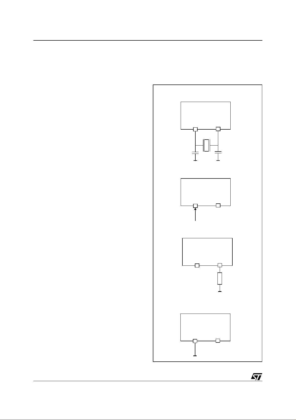
Figure 8. Os cill a tor C on f ig urations
CRYSTAL/RESONATOR CLOCK
CRYSTAL/RESONATOR option
ST6xxx
in
ST6xxx
in
ST6xxx
in
ST6xxx
in
OSC
OSC
NC
OSC
OSC
out
out
out
out
C
L2
R
NET
OSC
C
L1n
EXTERNAL CLOCK
CRYSTAL/RESONATOR option
OSC
RC NETWORK
RC NETW O RK option
OSC
NC
INTEGRATED CL OCK
CRYSTAL/RESONATOR option
OSG ENABLED option
OSC
18/78
NC
Page 19

ST62T52C ST62T62C/E62C
CLOCK SYSTEM (Cont’d)
Turning on the main oscillator is achieved by resetting the OSCOFF bit of the A/D Converter Control Register or by resetting the MCU. Restarting
the main oscillator implies a delay comprising the
oscillator start up delay period plus the duration of
the software instruction at f
clock frequency.
LFAO
3.1.2 Low Frequency Auxiliary Oscillator
(LFAO)
The Low Frequency Auxiliary Oscillator has three
main purposes. Firstly, it can be used to reduce
power consumption in non timing critical routines.
Secondly, it offers a fully integrated system clock,
without any external components. Lastly, it acts as
a safety oscillator in case of main oscillator failure.
This oscillator is available when the OSG ENABLED option is selected. In this case, it automatically starts one of its periods after the first missing
edge from the main oscillator, whatever the reason
(main oscillator defective, no clock circuitry provided, main osc illator swit ched off...).
User code, normal interrupts, WAIT and STOP instructions, are processed as normal, at the reduced f
frequency. The A/D converter accura-
LFAO
cy is decreased, since the internal frequency is below 1MHz.
At power on, the Low Frequency Aux ilia ry Osc ill ator starts faster than the Main Oscillator. It therefore feeds the on-chip counter generating the POR
delay until the Main Oscillator runs.
The Low Frequency Auxiliary Oscillator is automatically switched off as soon as the main oscillator sta r ts.
ADCR
Address: 0D1h — Read/Write
70
ADCR7ADCR6ADCR5ADCR4ADCR3OSC
OFF
ADCR1ADCR
0
Bit 7-3, 1-0= ADCR7-ADCR3, ADCR1-ADCR0:
ADC Control Register
. These bits are not used.
Bit 2 = OSCOFF. When low, this bit enables m ai n
oscillator to run. The main oscillator is switched off
when OSCOFF is high.
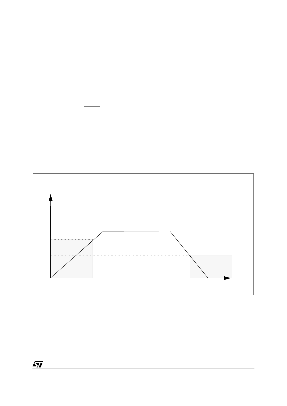
3.1.3 Oscillator Safe Guard
The Oscillator Safe Guard (OSG) affords drastically increased operational integrity in ST62x x dev ices. The OSG circuit provides three basic func-
tions: it filters spikes from the oscillator lines which
would result in over frequency to the ST62 CPU; it
gives access to the Low Frequency Auxiliary Oscillator (LFAO), used to ensure minimum processing in case of main oscillator failure, to offer reduced power consumption or to provide a fixed frequency low cost oscillator; finally, it automatically
limits the internal clock frequen cy as a function of
supply voltage, in order to ensure correct operation even if the power supply should drop.
The OSG is enabled or disab led by choosin g the
relevant OSG option. It may b e viewed as a filter
whose cross-over frequency is device dependent.
Spikes on the oscillator lines result in an effectively
increased internal clock frequency. In the absence
of an OSG circuit, this may lead to an over frequency for a given power supply voltage. The
OSG filters out such spikes (as illustr ated in Figure
9.). In all cases, when the OSG is active, the max-
imum internal clock frequency, f
f
, which is supply voltage dependent. T his re-
OSG
lationship is illustrated in Figure 12..
When the OSG is enabled, the Low Frequency
Auxiliary Oscillator may be accessed. This oscillator starts operating after the first missing edge of
the main oscillator (see Figu re 10.).
Over-frequency, at a given power supp ly level, is
seen by the OSG as spikes; it therefore filte rs out
some cycles in order that the internal clock frequency of the device is kept within the range t he
particular device can stand (depending o n V
and below f
: the maximum authorised frequen-
OSG
cy with OSG enabled.
Note. The OSG should be used wherever possible
as it provides maximum safet y. Care must be taken, however, as it ca n increase power consumption and reduce the maximum operating frequency
to f
OSG
.
Warning: Care has to be taken when using the
OSG, as the internal frequency is defined between
a minimum and a maximum value and is not accurate.
For precise timing measu remen ts, it is no t re commended to use the OSG and it should not be enabled in applications that use the SPI or the UART.
It should also be noted that power consum ption in
Stop mode is higher when the OSG is enabled
(around 50µA at nominal conditions and room
temperature).
, is limited to
INT
DD
),
19/78
Page 20
ST62T52C ST62T62C/E62C
CLOCK SYSTEM (Cont’d)
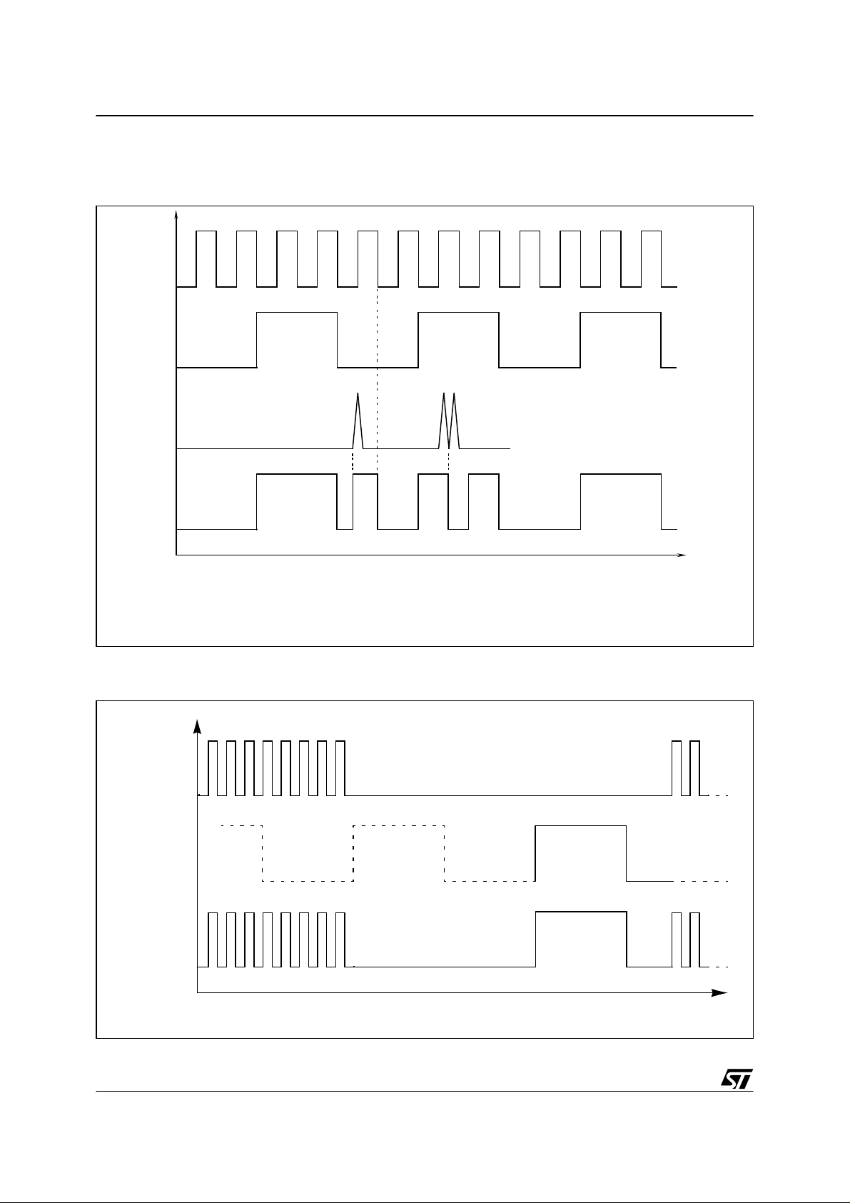
Figure 9. OSG Fi l terin g P rin c i pl e
(1)
(2)
(3)
(4)
(1)
Maximum Frequency for the device to work correctly
(2)
Actual Quartz Crystal Frequency at OSCin pin
(3)
Noise from OSCin
(4)
Resulting Internal Frequency
Figure 10. OSG Emergency Oscillator Principle
Main
Oscillator
Emergency
Oscillator
Internal
Frequency
VR001932
20/78
VR001933
Page 21
CLOCK SYSTEM (Cont’d)
Figure 11. Clock Circuit Block Diagram
ST62T52C ST62T62C/E62C
POR
OSG
MAIN
OSCILLATOR
LFAO
Main Oscillator off
Figure 12. Maximum Operating Frequency (f
Maximum FREQUENCY (MHz)
8
7
6
5
4
3
2
1
2.5
GUARANTEED
FUNCTIONALITY IS NOT
4
IN THIS AREA
3
3.644.555.56
M
U
X
) versus Supply Voltage (VDD)
MAX
3
2
1
f
INT
f
OSG
f
Min (at 85 °C)
OSG
f
Min (at 125°C)
OSG
:
:
12
13
:
Core
TIMER 1
Watchdog
1
SUPPLY VOLTAGE (V
Notes:
1. In this area, operation is guaranteed at the
quartz crystal frequency.
2. When the OSG is disabled, operation in this
area is guaranteed at the crystal frequency. When
the OSG is enabled, operation in this area is guaranteed at a frequency of at least f
OSG Min.
3. When the OSG is disabled, operation in this
)
DD
VR01807J
area is guaranteed at the quartz crystal frequency.
When the OSG is enab led, access to this area is
prevented. The internal frequency is kept a f
OSG.
4. When the OSG is disabled, operation in this
area is not guaranteed
When the OSG is enab led, access to this area is
prevented. The internal frequency is kept at f
OSG.
21/78
Page 22

ST62T52C ST62T62C/E62C
3.2 RESETS
The MCU can be reset in four ways:
– by the external Reset input being pulled low;
– by Power-on Reset;
– by the digital Watchdog peripheral timing out.
– by Low Voltage Detection (LVD)
3.2.1 RESET Input
The RESET
pin may be connected to a device of
the application board in order to reset the MCU if
required. The RESET
pin may be pulled low in
RUN, WAIT or STOP mode. This input can be
used to reset the MCU internal state and ensure a
correct start-up procedure. The pin i s active low
and features a Schmitt trigger input. The internal
Reset signal is generated by adding a delay to the
external signal. Therefore even short pulses on
the RESET
pin are acceptable, provide d VDD has
completed its rising phase and that the oscillator is
running correctly (normal RUN or WAIT modes).
The MCU is kept in the Reset state as long as the
RESET
If RESET
pin is held low.
activation occurs in the RUN or WAIT
modes, processing of the user program is stopped
(RUN mode only), the Inputs and Outputs are configured as inputs with pull-up resistors and the
main Osc illat o r is res t ar ted. When the le v el o n the
RESET pin then goes high, the initialization sequence is executed following expiry of the internal
delay period.
If RESET
pin activation occurs in the STOP mode,
the oscillator starts u p and a ll Inputs and Out puts
are configured as inputs with pull-up resistors.
When the level of the RESET
pin then goes high,
the initialization sequence is executed following
expiry of the internal delay period.
3.2.2 Power-on Reset
The function of the POR circuit cons ists in waking
up the MCU by detecting around 2V a dynamic
(rising edge) variation of the VDD Supply. At the
beginning of this sequence, the MCU is configured
in the Reset state: al l I/O ports are c onfigured as
inputs with pull-up resistors a nd no instruction is
executed. When the power supply voltage rises to
a sufficient level, the o scillator starts to operate,
whereupon an internal delay is initiated, in order to
allow the oscillator to fully stabilize befo re ex ecut ing the first instruction. The initialization sequence
is executed immediately following the internal delay.
To ensure correct s tart-up, the user shoul d take
care that the VDD Supply is stabilized at a sufficient level for the chosen frequency (see recommended operation) before the reset sign al is released. In addition, supply rising must start from
0V.
As a consequence, the POR does not allow to supervise static, slowly rising, or falling, or noisy
(present in g o s c illation) VDD supplies.
An external RC network connected to the RESET
pin, or the LVD reset can b e used instead to get
the best performances.
Figure 13. Reset and Interrupt Processing
RESET
NMI M ASK SET
INT LATCH CLEARED
( IF PRESENT )
SELECT
NMI MODE FLAGS
PUT FFEH
ON ADDRESS BUS
YES
IS RESET STILL
PRESENT?
NO
LOAD PC
FROM RESET LOCATIONS
FFE/FFF
FETCH INSTRUCTION
VA000427
22/78
Page 23
RESETS (Cont’d)
3.2.3 Watchdog Reset
The MCU provides a Wat chdog timer function in
order to ensure graceful recovery from software
upsets. If the Watchdog regi ster is not refreshed
before an end-of-count condition is reached, the
internal reset will be activated. This, amongs t ot her things, resets the watchdog counter.
ues, allowing hysteresis effect. Reference value in
case of voltage drop has been set lower than the
reference value for power-on in order to avoid any
parasitic Reset when MCU start's running and
sinking current on the supply.
As long as the s upply voltage is below the reference value, there is a internal and static RESET
command. The MCU can start only when the sup-
The MCU restarts just as though the Reset had
been generated by the RESET
pin, including the
built-in stabilisation de l a y peri o d.
3.2.4 LVD Reset
The on-chip Low Voltage Detector, selectable as
user option, features static Reset when supply
voltage is below a reference value. Thanks to this
feature, external reset circuit can be removed
while keeping the application safety. This SAFE
RESET is effective as well in Power-on phase as
ply voltage rises over the reference value. Therefore, only two operating mode exist for the MCU:
RESET active below the voltage reference, and
running mode over the voltage reference as
shown on the Figure 14., that represents a powerup, power-down sequence.
Note: When the RESET state is controlled by one
of the internal RESET sourc es (Low Voltage Detector, Watchdog, Power on Reset), the RESET
pin is tied to low logic level.
in power supply drop with different reference val-
Figure 14. LVD Reset on Power-on and Power-down (Brown-out)
ST62T52C ST62T62C/E62C
V
DD
V
Up
V
dn
RESET
3.2.5 Application Notes
No external resistor is requ ired bet ween V
DD
and
the Reset pin, thanks to the built-in pull-up device.
RESET
time
VR02106 A
Direct external connection of the pin RESET to
V
must be avoided in order to ensure safe be-
DD
haviour of the internal reset sources (AND.Wired
structure).
23/78
Page 24

ST62T52C ST62T62C/E62C
RESETS (Cont’d)
3.2.6 MCU Initialization Sequence
When a reset occurs the stack is reset, the PC is
loaded with the address of the Reset Vector (located in program ROM starting at address 0FFEh). A
jump to the beginning of the user program must be
coded at this address. Following a Reset , the Interrupt flag is automatically set, so that the CPU is
in Non Maskable Interrupt mode; this prevents the
initialisation routine from being interrupted. The initialisation routine should therefore be t erminated
by a RETI instruction, in order to revert to normal
mode and enable interrupts. If no pending interrupt
is present at the end of the initialisation routine, the
MCU will continue by processing the instruction
immediately following the RETI instruction. If, however, a pending interrupt is present, it will be serviced.
Figure 16. Reset Block Diagram
Figure 15. Reset and Interrupt Processing
RESET
RESET
VECTOR
INITIALIZATION
ROUTINE
JP
RETI
JP:2 BYTES/4 CYCLES
RETI: 1 BYTE/2 CYCLES
VA00181
V
DD
R
PU
R
RESET
POWER
WATCHDOG R ESE T
LVD RESET
1) Resis tive ESD protection. Val ue not guaranteed.
ESD
ON RESET
f
OSC
1)
AND. Wired
RESET
CK
COUNTER
RESET
ST6
INTERNAL
RESET
VR02107A
24/78
Page 25

RESETS (Cont’d)
Table 6. Register Reset Status
Register Address(es) Status Comment
EEPROM Control Register
Port Data Registers
Port Direction Register
Port Option Register
Interrupt Option Register
TIMER Status/Control
0EAh
0C0h to 0C2h
0C4h to 0C6h
0CCh to 0CEh
0C8h
0D4h
00h
ST62T52C ST62T62C/E62C
EEPROM enabled (if available)
I/O are Input with pull-up
I/O are Input with pull-up
I/O are Input with pull-up
Interrupt disabled
TIMER disabled
AR TIMER Mode Control Register
AR TIMER Status/Control 1 Register
AR TIMER Status/Control 2Register
AR TIMER Compare Register
X, Y, V, W, Register
Accumulator
Data RAM
Data RAM Page REgister
Data ROM Window Register
EEPROM
A/D Result Register
AR TIMER Load Register
AR TIMER Reload/Capture Register
TIMER Counter Register
TIMER Prescaler Register
Watchdog Counter Register
A/D Control Register
0D5h
0D6h
0D7h
0DAh
080H TO 083H
0FFh
084h to 0BFh
0E8h
0C9h
00h to F3h
0D0h
0DBh
0D9h
0D3h
0D2h
0D8h
0D1h
Undefined
FFh
7Fh
FEh
40h
AR TIMER stopped
As written if programmed
Max count loaded
A/D in Standby
25/78
Page 26

ST62T52C ST62T62C/E62C
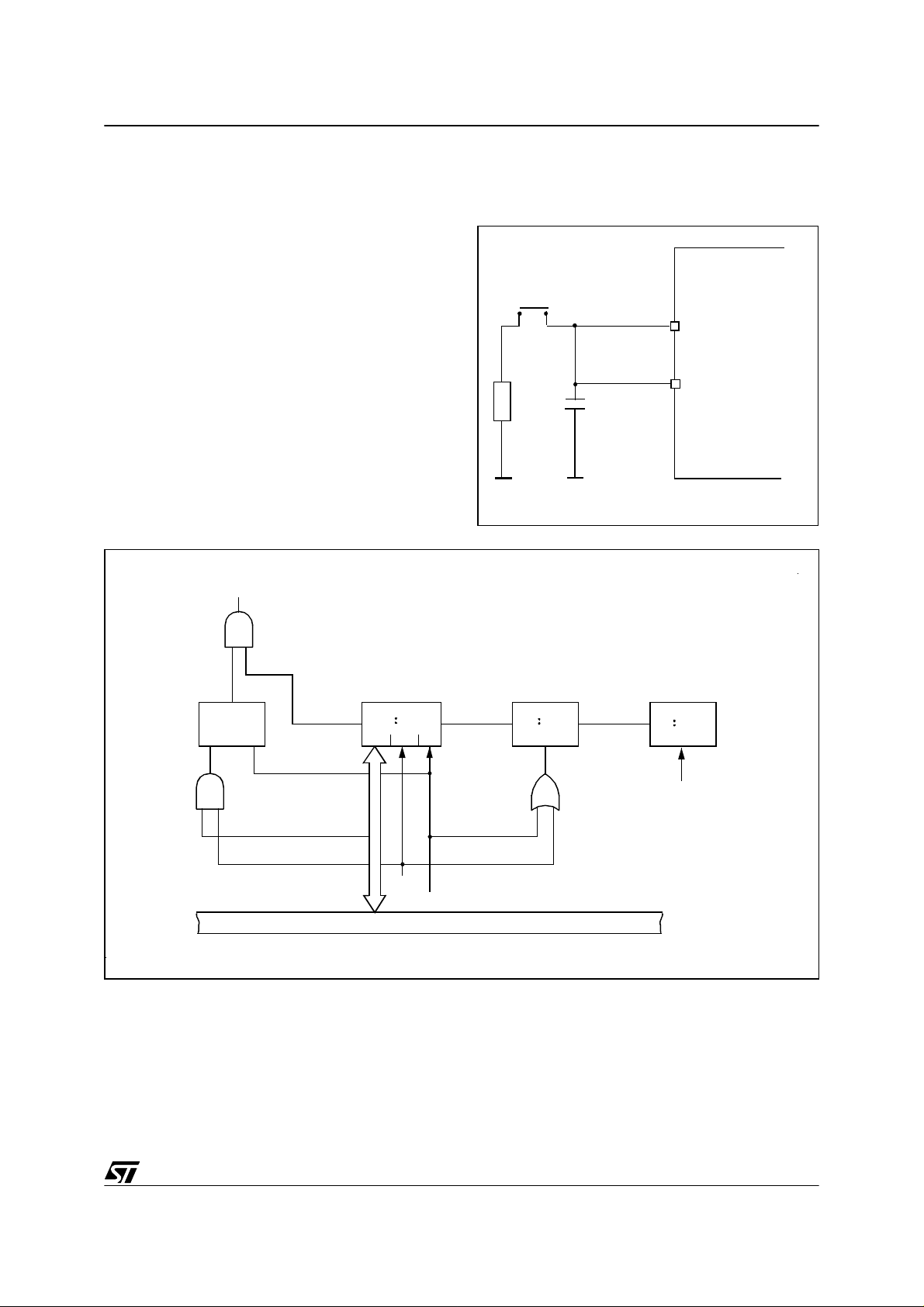
3.3 DIGITAL WATCHDOG
The digital Watchdog consists of a reloadable
downcounter timer which can be used to provide
controlled recovery from software upsets.
The Watchdog circuit generates a Reset when the
downcounter reaches zero. User software can
prevent this reset by reloading the counter, and
should therefore be written so that the counter is
regularly reloaded while the user program runs
correctly. In the event of a software mishap (usually caused by externally generated interference),
the user program will no longer behave in its usual
fashion and the timer register will thus not be reloaded periodically. Consequently the timer will
decrement down to 00h and reset the MCU. In order to maximise the effectiveness of the Watchdog
function, user software must be written with this
concept in mind.
Watchdog behaviour is gove rned by two options,
known as “WATCHDOG ACTIVATION” (i.e.
HARDWARE or SOFTWARE) and “EXTERNAL
STOP MODE CONTROL” (see Table 7 ).
In the SOFTWARE option, t he Watchdog is d isabled until bit C of the DWDR register has been set.
Table 7. Recommended Option Choices
Functions Required Recommended Options
Stop Mode & Watchdog “EXTERNAL STOP MODE” & “HARDWARE WATCHDOG”
Stop Mode “SOFTWARE WATCHDOG”
Watchdog “HARDWARE WATCHDOG”
When the Watchdog is di sabled, low power Stop
mode is available. On ce activated, the Watchdog
cannot be disabled, except by resetting the MCU.
In the HARDWARE option, the Watchdog i s permanently enabled. Since the oscillator will run continuously, low power mode is not available. The
STOP instruction is inter pr eted as a WAIT instr uc tion, and the Watchdog continues to countdown.
However, when the EXTERNAL STOP MODE
CONTROL option has been selected low power
consumption may be achieved in Stop Mode.
Execution of the STOP instruction is then governed by a secondary function associated with the
NMI pin. If a STOP instruction is encountered
when the NMI pin is low, it is interpreted as WAIT,
as described above. If, however, the STOP instruction is encountered when the NMI pin is high,
the Watchdog counter is fr ozen and the CPU enters STOP mode.
When the MCU exits STOP mode (i.e. when an interrupt is generated), the Watchdog resumes its
activity.
26/78
Page 27

DIGITAL WATCHDOG (Cont’d)
The Watchdog is associated with a Data space
register (Digital WatchDog Register, DWDR, location 0D8h) which is described in greater detail in
Section 3.3.1 Digital Watchdog Register (DWDR).
This register is set to 0FEh on Reset: bit C is
cleared to “0”, which disables the Watchdog; the
timer downcounter bits, T0 t o T5, and the SR bit
are all set to “1”, thus selecting the longest Watchdog timer period. This time period can be set to t he
user’s requirements by setting the appropriate value for bits T0 to T5 in the DWDR register. The SR
bit must be set to “1”, since it is this bit which generates the Reset signal when it changes to “0”;
clearing this bit would gen erate an i mm edia te Reset.
It should be noted that the order of the bits in the
DWDR register is inverted with respect to the associated bits in the down counter: bit 7 of the
DWDR register corresponds, in fact, to T0 and bit
2 to T5. The user should bear in mind the fact that
these bits are inverted and shifted with respect t o
the physical counter bits when writing to this register. The relationship between the DWDR regist er
bits and the physical implementation of the Watchdog timer downcounter is illustrated in Figure 17..
Only the 6 most significant bits may be used to define the time period, since it is bit 6 which triggers
the Reset when it changes to “0”. This offers the
user a choice of 64 timed periods ranging from
3,072 to 196,608 clock c ycles (with an oscillator
frequency of 8MHz, this is equivalent to t i mer periods ranging from 384µs to 24.576ms).
ST62T52C ST62T62C/E62C
Figure 17. Watchdog Counter Control
D0
D1
D2
D3
D4
D5
D6
WATCHDOG CONTROL REGISTER
D7
C
SR
RESET
T5
T4
T3
WATCHDOG COUNTER
T2
T1
T0
8
÷2
OSC ÷12
VR02068A
27/78
Page 28

ST62T52C ST62T62C/E62C
DIGITAL WATCHDOG (Cont’d)
3.3.1 Digital Watchdog Register (DWDR)
Address: 0D8h — Read/Write
Reset status: 1111 1110b
70
T0 T1 T2 T3 T4 T5 SR C
Bit 0 = C :
Watchdog Control bit
If the hardware option is selected, this bit is forced
high and the user cannot change it (the Watchdog
is always active). When the software option is selected, the Watchd og function is activated by set ting bit C to 1, and cannot then be disabled (save
by resetting the MCU).
When C is kept low the counter can be used as a
7-bit timer.
This bit is cleared to “0” on Reset.
Bit 1 = SR:
Software Reset bit
This bit triggers a Reset when cleared.
When C = “0” (Watchdog disabled) it is the MSB of
the 7-bit timer.
This bit is set to “1” on Reset.
Bits 2-7 = T5-T0:
Downcounter bits
It should be noted that the register bits are reversed and shifted with respect to the physical
counter: bit-7 (T0) is the LSB of the Watchdog
downcounter and bit-2 (T5) is the MSB.
These bits are set to “1” on Reset.
3.3.2 Application Notes
The Watchdog plays an i mportant support ing role
in the high noise immunity of ST62xx devices, and
should be used whe rever possible. Watchd og related options shou ld be select ed o n t he basis of a
trade-off between application s ecurity and STOP
mode availabilit y.
When STOP m ode is not requ ired, hardware activation without EXTERNAL STOP MODE CONTROL should be preferred, as it provides maximum security, especially during power-on.
When STOP mode i s required, hardware activation and EXTERNAL STOP MODE CONTROL
should be chosen. NM I shoul d be high by defa ult,
to allow STOP mode to be entered when the MCU
is idle.
The NMI pin can be connected to an I/O line (see
Figure 18.) to allow its state to be controlled by
software. The I/O line can then be used to keep
NMI low while Watchdog protection is required, or
to avoid noise or key bounce. When no more
processing is required, the I/O line is released and
the device placed in STOP mode for lowest power
consumption.
When software activation is selected and the
Watchdog is not activated, t he downcounter may
be used as a simple 7-bit timer (remember that the
bits are in reverse order).
The software activation opt ion should be chosen
only when the Watchdog counter is to be used as
a timer. To ensure the Watchdog has not been unexpectedly activated, the following instructions
should be executed within the first 27 instructions:
jrr 0, WD, #+3
ldi WD, 0FDH
28/78
Page 29
DIGITAL WATCHDOG (Cont’d)
These instructions test the C bit and Reset the
MCU (i.e. disable the Watchdog) i f the bit is set
(i.e. if the Watchdog is active), thus disabling the
Watchdog.
In all modes, a minimum of 28 instructions are executed after activation, before the Watchdog can
generate a Reset. Consequently, user software
should load the watchdog counter within the first
27 instructions following Watchdog activation
(software mode), or within the first 27 inst ructions
executed following a Reset (hardware activation).
It should be noted that when the GEN bit is low (interrupts disabled), the NMI interrupt is active but
cannot cause a wake up from STOP/WAIT modes.
Figure 19. Digital Watchdog Block Diagram
ST62T52C ST62T62C/E62C
Figure 18. A typical circuit maki ng use of the
EXERNAL STOP MODE CONTROL feature
SWITCH
NMI
I/O
VR02002
RESET
RSFF
S
Q
R
DB0
7
-2
DB1.7 SETLOAD
8
WRITE
DATA BUS
RESET
-2
SET
8
-12
OSCILLATOR
CLOCK
VA00010
29/78
Page 30

ST62T52C ST62T62C/E62C
3.4 INTERRUPTS
The CPU can manage four Maskable Interrupt
sources, in addition to a Non Maskable Interrupt
source (top priority interrupt). Each source i s associated with a specific Interrupt Vector which contains a Jump instruction to the associated interrupt
service routine. These vec tors are located i n Program space (see Table 8 ).
When an interrupt source generates an interrupt
request, and interrupt processing is enabled, the
PC register is loaded with the address of the interrupt vector (i.e. of the Jump instruction), which
then causes a Jump to the relevant interrupt service routine, thus servicing the interrupt.
Interrupt sources are linked to events either on external pins, or on chip peripherals. Several event s
can be ORed o n the same interrupt source, an d
relevant flags are available to determine which
event triggered the interrupt.
The Non Maskable Interrupt request has the highest priority and can interrupt any interrupt rou tine
at any time; the other four interrupts cannot interrupt each other. If more than one interrupt request
is pending, these are processed by the proces sor
core according to their priority level: source #1 has
the higher priority while source #4 the lower. The
priority of each interrupt source is fixed.
Table 8. Interrupt Vector Map
Interrupt Source Priority Vector Address
Interrupt source #0 1 (FFCh-FFDh)
Interrupt source #1 2 (FF6h-FF7h)
Interrupt source #2 3 (FF4h-FF5h)
Interrupt source #3 4 (FF2h-FF3h)
Interrupt source #4 5 (FF0h-FF1h)
3.4.1 Interrupt request
All interrupt sources but the Non M askable Interrupt source can be disabled by setting accordingly
the GEN bit of the Interrupt Option Register (IOR).
This GEN bit also defines if an interrupt source, including the Non Maskable Interrupt source, can restart the MCU from STOP/WAIT modes.
Interrupt request from the No n M ask able Interrupt
source #0 is latched by a flip flop which is automat-
ically reset by the core at the beginning of the nonmaskable interrupt service routine.
Interrupt request from source #1 can be configured either as edge or level sensitive by setting accordingly the LES bit of the Interrupt Option Register (IOR).
Interrupt request from source #2 are always edge
sensitive. The e dge polarity can be configured by
setting accord ingl y the ESB bit of the Int erru pt Option Register (IOR).
Interrupt request from sources #3 & #4 are level
sensitive.
In edge sensitive mode, a latch is set when a edge
occurs on the interrupt sou rce line and is cleared
when the associated interrupt routine is started.
So, the occurrence of an interrupt can be stored,
until completion of the running interrupt routine before being processed. If several interrupt requests
occurs before completion o f the running interrupt
routine, only the first request is stored.
Storage of interrupt requests is not available in level sensitive mode. To be taken into account, the
low level must be present on the interrupt pin when
the MCU samples the line after instruction execution.
At the end of every instruction, the MCU tests the
interrupt lines: if there is an interrupt request the
next instruction is not e xecuted and the appropriate interrupt service routine is executed instead.
Table 9. Interrupt Option Register Description
GEN
ESB
LES
OTHERS NOT USED
SET Enable all interrupts
CLEARED Disable all interrupts
SET
CLEARED
SET
CLEARED
Rising edge mode on interrupt source #2
Falling edge mode on interrupt source #2
Level-sensitive mode on interrupt source #1
Falling edge mode on interrupt source #1
30/78
Page 31

INTERRUPTS (Cont’d)
3.4.2 Interrupt Procedure
The interrupt procedure is very similar to a call procedure, indeed the user can consider the interrupt
as an asynchronous call procedure. As this is an
asynchronous event, the user cannot know the
context and the time at which it occurred. As a result, the user should save all Data space registers
which may be used within the interrupt routines.
There are separate sets of processor flags for normal, interrupt and non-maskable interrupt modes,
which are automatically switched and so do not
need to be saved.
The following list summarizes the interrupt procedure:
MCU
– The interrupt is detected.
– The C and Z flags are replaced by the interrupt
flags (or by the NMI flags).
– The PC contents are stored in the first level of
the stack.
– The normal interrupt lines are inhibited (NMI still
active).
– The first internal latch is cleared.
– The associated interrupt vector is loaded in the PC.
WARNING: In some circumstances, when a
maskable interrupt occurs while the ST6 core is in
NORMAL mode and es pecially during the ex ecution of an "ldi IOR, 00h" instruction (disabling all
maskable interrupts): if the interrupt arrives during
the first 3 cycles of the "ldi" instruction (which is a
4-cycle instruction) the core will switch to interrupt
mode BUT the flags CN and ZN will NOT switch to
the interrupt pair CI and ZI.
User
– User selected registers are saved within the in-
terrupt service routine (normally on a software
stack).
– The source of the interrupt is found by polling the
interrupt flags (if more than one source is associ-
ated with the same vector).
– The interrupt is serviced.
– Return from interrupt (RETI)
ST62T52C ST62T62C/E62C
MCU
– Automatically the MCU switches back to the nor-
mal flag set (or the interrupt flag set) and pops
the previous PC value from the stack.
The interrupt routine usually begins by the identifying the device which generated the interrupt request (by polling). The user should save the registers which are used within the interrupt routine in a
software stack. After the RETI instruction is executed, the MCU returns to the main routine.
Figure 20. Interrupt Processing Flow Chart
INSTRUCTION
FETCH
INSTRUCTION
EXECUTE
INSTRUCTION
LOAD PC FROM
INTERRUPT VECTOR
(FFC/FFD)
SET
INTERRUPT MASK
PUSH THE
PC INTO THE STACK
SELECT
INTERNAL MODE FLAG
VA000014
THE INSTRUCTION
YES
INTERRUPT MASK
PROGRAM FLAGS
THE STACKED PC
NO
WAS
A RETI ?
?
CLEAR
SELECT
"POP"
?
NO
YES
IS THE CORE
ALREADY IN
NORMAL MODE?
NO
CHECK IF THERE IS
AN INTERRUPT REQUEST
AND INTERRUPT MASK
YES
31/78
Page 32

ST62T52C ST62T62C/E62C
INTERRUPTS (Cont’d)
3.4.3 Interrupt Option Register (IOR)
The Interrupt Option Register (IOR) is used to enable/disable the individual interrupt sources and to
select the operating mode of the external interrupt
inputs. This register is write-only and cannot be
accessed by single-bit operations.
Address: 0C8h — Write Only
Reset status: 00h
70
- LES ESB GEN - - - -
Bit 5 = ESB:
The bit ESB selects the polarity of the interrupt
source #2.
Bit 4 = GEN:
is set to one, all interrupts are enable d. When t his
bit is cleared to zero a ll the interrupts (excluding
NMI) are disabled.
When the GEN bit is low, the NMI in terrupt is active but cannot cause a wake up from STOP/WAIT
modes.
This register is cleared on reset.
3.4.4 Interrupt Sources
Edge Selection bit
Global Enable Interrupt
.
. When this bit
Bit 7, Bits 3-0 =
Bit 6 = LES:
Unused
.
Level/Edge Selection bit
.
When this bit is set to one, the interrupt source #1
Interrupt sources available on the
ST62E62C/T62C are summarized in the Table 10
with associated mas k bit to enable/disabl e the in-
terrupt request.
is level sensitive. When cleared to zero the edge
sensitive mode for interrupt request is selected.
Table 10. Interrupt Requests and Mask Bits
Peripheral Register
GENERAL IOR C8h GEN
TIMER TSCR1 D4h ETI TMZ: TIMER Overflow Vector 4
A/D CONVERTER ADCR D1h EAI EOC: End of Conversion Vector 4
AR TIMER ARMC D5h
Port PAn ORPA-DRPA C0h-C4h ORPAn-DRPAn PAn pin Vector 1
Port PBn ORPB-DRPB C1h-C5h ORPBn-DRPBn PBn pin Vector 1
Port PCn ORPC-DRPC C2h-C6h ORPCn-DRPCn PCn pin Vector 2
Address
Register
Mask bit Masked Interrupt Source
All Interrupts, excluding NMI
OVIE
CPIE
EIE
OVF: AR TIMER Overflow
CPF: Successful compare
EF: Active edge on ARTIMin
Interrupt
vector
Vector 3
32/78
Page 33

INTERRUPTS (Cont’d)
Figure 21. Interrupt Blo ck D ia gram
FROM REGISTER PORT A,B,C
SINGLE BI T ENABLE
PBE
V
DD
ST62T52C ST62T62C/E62C
PORT A
PORT B
Bits
PORT C
Bits
PBE
PBE
SPIDIV Register
SPINT bi t
SPIE bit
SPIMOD Register
AR TIMER
V
DD
TIMER1
ADC
FF
QCLK
CLR
IOR REG. C8H, bit 5
OVF
OVIE
CPF
CPIE
EF
EIE
TMZ
ETI
EOC
EAI
0
MUX
Start
I
1
1
IOR REG. C8H, bit 6
FF
CLK Q
CLR
I2Start
INT #1 (F F6 ,7)
RESTART FROM
STOP/WAIT
INT #2 (F F4 ,5)
INT #3 (F F2 ,3)
INT #4 (F F0 ,1)
NMI
FF
QCLK
CLR
I
Start
0
Bit GEN (IOR Register)
NMI (FFC,D)
VA0426K
33/78
Page 34

ST62T52C ST62T62C/E62C
3.5 POWER SAVI NG MO DE S
The WAIT and STOP modes have been implemented in the ST62xx family of MCUs in order to
reduce the product’s electrical consumption during
idle periods. These two powe r saving modes are
described in the following paragraphs.
3.5.1 WAIT Mode
The MCU goes into WAIT mode as soon as the
WAIT instruction is executed. The microcontroller
can be considered as being in a “software f rozen”
state where the core stops processing the program instructions, the RAM contents and peripheral registers are preserved as long as the power
supply voltage is higher than the RAM retention
voltage. In this mode the peripherals are still active.
WAIT mode can be used when the use r wants to
reduce the MCU power consumption during idle
periods, while not losing track of time or the capability of monitoring external events. The active oscillator is not stopped in order to provide a clock
signal to the peripherals. Timer counting may be
enabled as well as the Timer interrupt, before entering the WAIT mode: this allows the WAIT mode
to be exited when a T imer interrupt occurs. Th e
same applies to other peripherals which use th e
clock signal.
If the WAIT mode is exited due to a Reset (either
by activating the external pin or generated by the
Watchdog), the MCU enters a normal reset procedure. If an interrupt is generated during WAIT
mode, the MCU’s behaviour depends on the stat e
of the processor core prior to the WAIT instruction,
but also on the kind of interrupt request which is
generated. This is described in the following para-
graphs. The processor core does not generate a
delay following the occurrence of the interrupt, be-
cause the oscillator clock is still av ailable and no
stabilisation period is necessary.
3.5.2 STOP Mode
If the Watchdog is disabled, STOP mode is availa-
ble. When in STOP mode, the MCU is pla ced in
the lowest power consumption mode. In this oper-
ating mode, the microcontroller can be considered
as being “frozen”, no instruction is e xecuted, the
oscillator is stopped, the RAM contents and pe-
ripheral registers are preserved as long as the
power supply voltage is higher than the RAM re-
tention voltage, and the ST62xx core wa its for the
occurrence of an external interrupt request or a
Reset to exit the STOP state.
If the STOP state is exited due to a Reset (by acti-
vating the external p in) the MCU will enter a nor-
mal reset procedure. Behaviour in response to in-
terrupts depends on the state of the processor
core prior to issuing the STOP instruction, and
also on the kind of interrupt request that is gener-
ated.
This case will be described in the following para-
graphs. The proces sor core generates a de lay a f-
ter occurrence of the interrupt request, in order to
wait for complete stabilisation of the oscillator, be-
fore executing the first instruction.
34/78
Page 35

POWER SAVING MODE (Cont’d)
3.5.3 Exit from WAIT and STOP Modes
The following paragraphs describe how the MCU
exits from WAIT and STOP modes, when an interrupt occurs (not a Reset). It should be noted that
the restart sequence depends on the original state
of the MCU (normal, interrupt or non-maskable interrupt mode) prior to entering WAIT or STOP
mode, as well as on the interrupt type.
Interrupts do not affect the oscillator selection.
3.5.3.1 Normal Mode
If the MCU was in the main routine when the WAIT
or STOP instruction was executed, exit from S top
or Wait mode will occur as soon as an interrupt occurs; the related interrupt routine is executed and,
on completion, the instruction which follows the
STOP or WAIT instruction is then executed, providing no other interrupts are pending.
3.5.3.2 Non Maskable Interrupt Mode
If the STOP or WAIT instruc tion has be en ex ecut ed during execution of the non-maskab le interrupt
routine, the MCU exits from the Stop or Wait mode
as soon as an interrupt occurs: the instruction
which follows the STOP or WAIT instruction is executed, and the MCU remains in non-maskable interrupt mode, even if another interrupt has been
generated.
3.5.3.3 Normal Interrupt Mode
If the MCU was in interrupt mode before the STOP
or WAIT instruction was executed, it exits from
STOP or WAIT mode as soon as an interrupt occurs. Nevertheless, two cases must be considered:
– If the interrupt is a normal one, the interrupt rou-
tine in which the WAIT or STOP mode was en-
ST62T52C ST62T62C/E62C
tered will be completed, starting with the
execution of the instruction which follows the
STOP or the WAIT instruction, and the MCU is
still in the interrupt mode. A t the end of this routine pending interrupts will be serviced in accordance with their priority.
– In the event of a non-maskable interrupt, the
non-maskable inte rrupt service routine is processed first, then the routine in which the WAIT or
STOP mode was entered will be compl eted by
executing the instruction following the STOP or
WAIT instruction. The MCU remains in normal
interrupt mode.
Notes:
To achieve the lowest po wer consumption during
RUN or WAIT modes, the user program must take
care of:
– configuring unused I/Os as inputs without pull-up
(these should be ext ernally tied to well defined
logic levels);
– placing all peripherals in their power down
modes before entering STOP mod e;
When the hardware activated Watchdog i s sel ect-
ed, or when the software Watchdog is enabled, the
STOP instruction is disabled and a WAIT instruc-
tion will be executed in its place.
If all interrupt sources are disabled (GEN low), the
MCU can only be restarted by a Reset. Although
setting GEN low does not mask the NMI as an in-
terrupt, it will stop it generating a wake-up signal.
The WAIT and STOP instructions are not execut-
ed if an enabled interrupt request is pending.
35/78
Page 36

ST62T52C ST62T62C/E62C
4 ON-CHIP PERIPHERALS
4.1 I/O PORTS
The MCU features Input/Output lines which m ay
be individually programmed as any of the following
input or output configurations:
– Input without pull-up or interrupt
– Input with pull-up and interrupt
– Input with pull-up, but without interrupt
– Analog input
– Push-pull output
– Open drain output
The lines are organised as bytewise Ports.
Each port is associated with 3 registers in Data
space. Each bit of these registers is associated
with a particular line (for instance, bits 0 of Port A
Data, Direction and Option registers are associated with the PA0 line of Port A).
The DATA registers (DRx), are used to read the
voltage level values of the lines which have bee n
configured as inputs, or t o write the logic value of
the signal to be output on the l ines configured as
outputs. The port data registers can be read to get
the effective logic levels of the pins, but t hey can
Figure 22. I/O Por t Bl ock D i agram
SIN CONTRO LS
RESET
be also written by user software, in conjunction
with the related option registers, to select the dif-
ferent input mode options.
Single-bit operations on I/O registers a re possible
but care is necessary because reading in input
mode is done from I/O pins while writing will direct-
ly affect the Port data register ca using an unde-
sired change of the input configuration.
The Data Direction registers (DDRx) allow the
data direction (input or output) of each pin to be
set.
The Option registers (ORx) are used to select the
different port options available both in input and in
output mode.
All I/O registers can be read or written to just as
any other RAM location in Data space, so no extra
RAM cells are needed for port data storage and
manipulation. During MCU initialization, all I/O reg-
isters are cleared and the input mode with pull-ups
and no interrupt generation is se lected for all the
pins, thus avoiding pin conflicts.
V
DD
36/78
SHIFT
REGISTER
S
OUT
TO INTERRUPT
TO ADC
DATA
DIRECTION
REGISTER
DATA
REGISTER
OPTION
REGISTER
V
DD
INPUT/OUTPUT
VA00413
Page 37

ST62T52C ST62T62C/E62C
I/O PO R T S (Cont’d)
4.1.1 Operating Modes
Each pin may be individually programmed as input
or output with various configurations.
This is achieved by writing the relevant bit in the
Data (DR), Data Direction (DDR) and O ption registers (OR). Table 11 illustrates the various port
configurations which can be selected by user software.
4.1.1.1 Input Options
Pull-up, High Impedance Option. All input lines
can be individually programmed with or without an
internal pull-up by programming the OR and DR
registers accordingly. If the pull-up option is not
selected, the input pin will be in the high-impedance state.
Table 11. I/O Port Option Selection
DDR OR DR Mo de Option
0 0 0 Input With pull-up, no interrupt
0 0 1 Input No pull-up, no interrupt
0 1 0 Input With pull-up and with interrupt
0 1 1 Input Analog input (when available)
1 0 X Output Open-drain output (20mA sink when available)
1 1 X Output Push-pull output (20mA sink when available)
4.1.1.2 Interrupt Options
All input lines can be individually connected by
software to the interrupt system by programming
the OR and DR registers accordingly. The inter-
rupt trigger modes (fall ing edge, rising edge and
low level) can be configured by software as de-
scribed in the Interrupt Chapter for each port.
4.1.1.3 Analog Input Options
Some pins can be configured as analog input s by
programming the OR and DR registers according-
ly. These analog inputs are c onnected to the on-
chip 8-bit Analog to Digital Converter.
pin should be programmed as an a nalog input at
any time, since by selecting m ore than one input
simultaneously their pins will be effectively sh ort-
ed.
ONLY ONE
Note: X = Don’t care
37/78
Page 38

ST62T52C ST62T62C/E62C
I/O PO R T S (Cont’d)
4.1.2 Safe I/O State Switching Sequence
Switching the I/O ports from one state to another
should be done in a se quence which ensures that
no unwanted side effects can occur. The recommended safe transitions are illustrated in Figure
23.. All other transitions are potentially risky and
should be avoided when changing the I/O operating mode, as it is most likely that undesirable sideeffects will be experienced, such as spurious interrupt generation or two pins shorted together by the
analog multiplexer.
Single bit instructions (SET, RES, INC and DEC)
should be used with great caution on Ports Data
registers, since these instructions make an implicit
read and write back of the entire reg ister. In port
input mode, however, the data register reads from
the input pins directly, and not from the data register latches. Since data register information in input
mode is used to set the characteristics of the input
pin (interrupt, pull-up, analog input), these may be
unintentionally reprogrammed depending on the
state of the input pins. As a general rule, it is better
to limit the use of single bit instructions on data
registers to when the whole (8-bit) port is in output
mode. In the case of inputs or of mixed inputs and
outputs, it is advisable to keep a copy of the data
register in RAM. Single bit instructions may then
be used on the R AM copy, a fter which the whole
copy register can be written to the port data regis-
ter:
SET bit, datacopy
LD a, datacopy
LD DRA, a
Warning: Care must also be taken to not use in-
structions that act on a whole port register (INC,
DEC, or read operations) when all 8 bits are not
available on the de vice. Unavailable bits must be
masked by software (AND instruction).
The WAIT and STOP instructions allow the
ST62xx to be used in situations where low power
consumption is needed. The lowest power con-
sumption is achieved b y configuring I/Os in input
mode with well-defined logic levels.
The user must take care not to switch outputs with
heavy loads during the co nversion of one of the
analog inputs in order to avoid any disturbance to
the conversion.
Figure 23. Diagram showing Safe I/O State Transitions
Interrupt
pull-up
010*
Input
pull-up (Reset
000
state)
Output
Open Drain
Output
Push-pull
100
110
Note *. xxx = DDR, OR, DR Bits respectively
011
001
101
111
Input
Analog
Input
Output
Open Drain
Output
Push-pull
38/78
Page 39

I/O PO R T S (Cont’d)
Table 12. I/O Port Option Selections
ST62T52C ST62T62C/E62C
MODE AVAILABLE ON
Input
Reset state(
Reset state if PULL-UP
option disabled
Input
Reset state
Reset state if PULL-UP
option enabled
Input
with pull up
with interrupt
(1)
PA4-PA5
PB0, PB6-PB7
PC2-PC3
PB2-PB3,
PA4-PA5
PB0,,PB6-PB7
PC2-PC3
PB2-PB3
PA4-PA5
PB0, PB2-PB3,PB6-PB7
PC2-PC3
SCHEMATIC
Data in
Interrupt
Data in
Interrupt
Data in
Interrupt
Analog Input
Open drain output
5mA
Open drain output
30mA
Push-pull output
5mA
Push-pull output
30mA
Note 1. Pr ovided the cor rect configuration has been selected.
PA4-PA5
PC2-PC3
PA4-PA5
PC2-PC3
PB0, PB2-PB3,PB6-PB7
PA4-PA5
PC2-PC3
PB0, PB2-PB3,PB6-PB7
ADC
Data out
Data out
39/78
Page 40

ST62T52C ST62T62C/E62C
I/O PO R T S (Cont’d)
4.1.3 ARTimer alternate functions
When bit PWMOE of register ARMC is low, pin
ARTIMout/PB7 is configured as any standard pin
of port B through the port registers. When PWMOE is high, ARTMout/PB7 is the PWM output, independently of the port registers configuration.
Figure 24. Peripheral Interface Configuration of AR Timer
ARTIMin/PB6 is c onnect ed to t he A R Timer input.
It is configured through the port regist ers as any
standard pin of port B. To use ARTIMin/PB6 as AR
Timer input, it must be configured as input through
DDRB.
PID
ARTIMin
ARTIMin
ARTIMout
PID
DR
MUX
AR TIMER
OR
1
0
DR
PWMOE
ARTIMout
VR01661G
40/78
Page 41

4.2 TIMER
ST62T52C ST62T62C/E62C
The MCU features an on-chip Timer peripheral,
consisting of an 8-bit counter with a 7-bit programmable prescaler, giving a maximum count of 2
15
.
Figure 25. shows the Time r Block Diagram. The
content of the 8-bit counter can be read/written in
the Timer/Counter register, TCR, which can be addressed in Data space as a RAM location at address 0D3h. The state of the 7-bit prescaler can be
read in the PSC register at address 0D2h. The
control logic device is managed in the TSCR register as described in the following paragraphs.
The 8-bit counter is decrement by the output (rising edge) coming from the 7-bit prescaler and can
be loaded and read under program contro l. Whe n
it decrements to zero then the TMZ (Timer Zero)bit
in the TSCR is set. If the ETI (Enable Timer Interrupt) bit in the TSCR is also set, an interrupt request is generated. The Timer interrupt can be
used to exit the MCU from WAIT mode.
Figure 25. Timer Block Diagram
The prescaler input is the interna l frequency (f
divided by 12. The p rescaler decrements on the
rising edge. Depending on the division factor pro-
grammed by P S2, PS 1 and PS0 bits in the TSCR
(see Table 13.), the clock input of the timer/coun-
ter register is multiplexed to different s ources . For
division factor 1, the clock input of the prescaler is
also that of timer/counter; for factor 2, bit 0 of the
prescaler register is connected to the clock input of
TCR. This bit changes its state at half the frequen-
cy of the prescaler input clock. For factor 4, bit 1 of
the PSC is connected to the clock input of TCR,
and so forth. The prescaler initialize bit, PSI, in the
TSCR register must be set to allow the prescaler
(and hence the counter) to start. If it is cleared, all
the prescaler bits are se t and t he counter is inhib-
ited from counting. The prescaler can be loa ded
with any value between 0 and 7Fh, if bit PSI is set.
The prescaler tap is selected by means of the
PS2/PS1/PS0 bits in the control register.
Figure 26. illustrates the Timer’s working principle.
DATA BUS
INT
)
f
INT
12
PSC
8
6
5
4
3
2
1
0
SELECT
1 OF 7
8
8-BIT
COUNTER
3
b7 b6 b5 b4 b3 b2 b1 b0
STATUS/CONTROL
TMZ ETI D5 D4 PSI PS2 PS1 PS0
8
REGISTER
INTERRUPT
LINE
VR02070A
41/78
Page 42

ST62T52C ST62T62C/E62C
TIMER (Cont’d)
4.2.1 Timer Operation
The Timer prescaler is clocked by the prescaler
clock input (f
The user can select the desired prescaler division
ratio through t he PS2, P S1, PS0 b its. When the
TCR count reaches 0, it sets the TMZ bit in the
TSCR. The TMZ bit can be tested und er program
control to perform a timer function whenever it
goes high.
4.2.2 Timer Interru pt
When the counter register decrements to zero with
the ETI (Enable Timer Interrupt) bit s et to one, a n
interrupt request associated with Interrupt Vector
#4 is generated. When the c ounter dec rem ents t o
Figure 26. Tim er Working Princ i pl e
CLOCK
÷ 12).
INT
BIT0 BIT1 BIT2
7-BIT PRESCALE R
zero, the TMZ bit in the TSCR register is set to
one.
4.2.3 Application Notes
TMZ is set when the counter reaches zero; howev-
er, it may also be set by writing 00h in the TCR
register or by setting bit 7 of the TSCR register.
The TMZ bit must be cleared by user software
when servicing the timer interrupt to avoid unde-
sired interrupts when leaving the interrupt service
routine. After reset, the 8-bit counter register is
loaded with 0FFh, while the 7-bit prescaler is load-
ed with 07Fh, and the TSCR register is cleared.
This means that the Timer is stopped (PSI=“0”)
and the timer interrupt is disabled.
BIT3 BIT6BIT5BIT4
10234
8-1 MULTIPLEXER
BIT0 BIT1
BIT2
BIT3 BIT4 BIT5 BIT6
8-BIT COUNTER
5
67
BIT7
PS0
PS1
PS2
VA00186
42/78
Page 43

ST62T52C ST62T62C/E62C
TIMER (Cont’d)
A write to the TCR register will predominate over
the 8-bit counter decrement to 00h function, i.e. if a
write and a TCR register decrement to 00h occur
simultaneously, the write will take precedence,
and the TMZ bit i s not set until the 8-bit c ounter
reaches 00h again. The values of the TCR and the
PSC registers can be read accurately at any time.
4.2.4 Timer Registers
Timer Status Control Register (TSCR)
Address: 0D4h — Read/Write
70
TMZ ETI D5 D4 PSI PS2 PS1 PS0
Bit 7 = TMZ:
Timer Ze r o bit
A low-to-high transition indicates that the timer
count register has decrement to zero. This bit
must be cleared by user software before starting a
new count.
Bit 6 = ETI:
Enable Timer Interrup
When set, enables the timer interrupt request
(vector #4). If ETI=0 the timer interrupt is di sabled.
If ETI=1 and TMZ=1 an interrupt request is generated.
Bit 5 = D5:
Reserved
Must be set to “1”.
Bit 4 = D4
Do not care.
Bit 3 = PSI:
Prescaler Initialize Bit
Used to initialize the prescaler and inhibit its counting. When PSI=“0” the presc aler is set to 7Fh and
the counter is inhibited. When PSI=“1” the prescaler is enabled to count downwards. As long as
PSI=“0” both counter and prescaler are not run-
ning.
Bit 2, 1, 0 = PS2, PS1, PS0:
These bits select the division ratio of the pres-
lect.
caler register.
Table 13. Prescaler Division Factors
PS2 PS1 PS0 Divided by
0 0 0 1
0 0 1 2
0 1 0 4
0118
10016
10132
11064
111128
Timer Counter Register (TCR)
Address: 0D3h — Read/Write
70
D7 D6 D5 D4 D3 D2 D1 D0
Bit 7-0 = D7-D0:
Counter Bits.
Prescaler Register PSC
Address: 0D2h — Read/Write
70
D7 D6 D5 D4 D3 D2 D1 D0
Bit 7 = D7: Always read as "0".
Bit 6-0 = D6-D0: Prescaler Bit s .
Prescaler Mux. Se-
43/78
Page 44

ST62T52C ST62T62C/E62C
4.3 AUTO-RELOAD TIMER
The Auto-Reload Timer (AR Timer) on-chip peripheral consists of an 8-bit timer/counter with
compare and cap ture/reload capabilities and of a
7-bit prescaler with a clock m ultiplexer, enabling
the clock input to be selected as f
external clock source. A Mode Control Register,
INT
, f
INT/3
or an
ARMC, two Status Control Registers, ARSC0 and
ARSC1, an output pin, ARTIMout, and an input
pin, ARTIMin, allow the Auto-Reload Timer to be
used in 4 modes:
– Auto-reload (PWM generation),
– Output compare and reload on externa l event
(PLL),
– Input capture and output compare for time meas-
urement.
– Input capture and output compare for period
measurement.
The AR Timer can be used to wake the MCU from
WAIT mode either with an internal or with an external clock. It also can be used to wake the MCU
from STOP mode , if used with an external clock
signal connected to the ARTIMin pin. A Load register allows the program to read and write the
counter on the fly.
4.3.1 AR Timer Description
The AR COUNTER is an 8-bit up-counter incremented on the input clock’s rising edge. The counter is loaded from the ReLoad/Capture Register,
ARRC, for auto-reload or capture operations, as
well as f or initialization. Direct access to the AR
counter is not possible; however, by reading or
writing the ARLR load register, it is possible to
read or write the counter’s contents on the fly.
The AR Timer’s input clock can be either the internal clock (from the Oscillator Divider), the internal
clock divided by 3, or the clock signal connected to
the ARTIMin pin. Selection between these clock
sources is effected by suitably programming bits
CC0-CC1 of the ARSC1 register. The output of the
AR Multiplexer feeds the 7-bit programmable AR
Prescaler, ARPSC, which selects one of the 8
available taps of the prescaler, as defined by
PSC0-PSC2 in the AR Mode Control Register.
Thus the division factor of the prescaler can be set
to 2n (where n = 0, 1,..7).
The clock input to the AR counter is enabled by the
TEN (Timer Enable) bit in the ARMC register.
When TEN is reset, the AR counter is stopped and
the prescaler and counter contents are frozen.
When TEN is set, the AR counter runs at the rate
of the selected clock source. The counter is
cleared on system reset.
The AR counter may also be initialized by writing
to the ARLR load register, which also causes an
immediate copy of the value to be placed in the AR
counter, regardless of whether the counter is run-
ning or not. I nitialization of the counter, by either
method, will also clear the ARPSC register, where-
upon counting will start from a known value.
4.3.2 Timer Operating Modes
Four different operating modes are available for
the AR Timer:
Auto-reload Mode with PWM Generation. This
mode allows a Pulse Width Modulated signal to be
generated on the ARTIMout pin with minimum
Core processing overhead.
The free running 8-bit counter is fed by the pres-
caler’s output, and is incremented on every rising
edge of the clock signal.
When a counter overflow occurs, the counter is
automatically reloaded with the contents of the Re-
load/Capture Register, ARCC, and ARTIMout is
set. When the counter reaches the value con-
tained in the compare register (ARCP), ARTIMout
is reset.
On overflow, the OVF flag of the ARSC0 register is
set and an overflow interrupt request is generated
if the overflow interrupt enable bit, OVIE, in the
Mode Control Register (A RMC), is set. The OVF
flag must be reset by the user software.
When the counter reaches the compare value, the
CPF flag of t he A RS C0 register is set a nd a com-
pare interrupt request is generated, if t he Compare
Interrupt enable bit, CPIE, in the Mode Control
Register (ARMC), is set. The interrupt service rou-
tine may then adjust the PWM period by loading a
new value into ARCP. The CPF flag must be reset
by user software.
The PWM signal is generated on the ARTIMout
pin (refer to the Block Diagram). The f requen cy of
this signal is controlled by the prescaler setting
and by the auto-reload value present in the Re-
load/Capture register, ARRC. The duty cycle of
the PWM signal is controlled by the Compare Reg-
ister, ARCP.
44/78
Page 45

AUTO-RELOAD TIMER (Cont’d)
Figure 27. AR Timer Block Diagram
ST62T52C ST62T62C/E62C
f
f
INT
INT
/3
M
U
X
CC0-CC1
7-Bit
AR PRES CA LE R
PS0-PS2
DATA BUS
8
AR COMPARE
REGISTER
8
COMPARE
8
8-Bit
AR COUNTER
8
CPF
OVF
LOAD
DRB7
R
S
OVF
OVIE
TCLD
EIE
EF
CPF
CPIE
DDRB7
PB7/
ARTIMout
PWMOE
AR TIMER
INTERRUPT
PB6/
ARTIMin
SL0-SL1
SYNCHRO
EF
88
AR
RELOAD/CAPTURE
REGISTER
8
AR
LOAD
REGISTER
8
DATA BUS
VR01660A
45/78
Page 46

ST62T52C ST62T62C/E62C
AUTO-RELOAD TIMER (Cont’d)
It should be noted that the reload val ues will also
affect the value and the resolution of the duty cycle
of PWM output signal. To obtain a signal on ARTIMout, the contents of the ARCP register must be
greater than the contents of the ARRC register.
The maximum available resolution for the ARTIMout duty cycle is:
Resolution = 1/[255-(ARRC)]
Where ARRC is the content of the Reload/Capture
register. The compare value loaded in the Com pare Register, ARCP, must be in the range from
(ARRC) to 255.
Figure 28. Auto-reload Timer PWM Function
COUNTER
255
COMPARE
VALUE
The ARTC counter is initialized by writing to t he
ARRC register and by then setting the TCLD (Tim-
er Load) and the TEN (Timer Clock Enable) bits in
the Mode Control register, ARMC.
Enabling and sel ection of t he c lock s ource is con-
trolled by the CC0, CC1, SL0 and S L1 bits in the
Status Control Register, ARSC1. The prescaler di-
vision ratio is selected by the P S0, PS1 and PS 2
bits in the ARSC1 register.
In Auto-reload Mode, any of the three available
clock sources can be selected: Internal Clock, In-
ternal Clock divided by 3 or the clock signal
present on the ARTIMin pin.
RELOAD
REGISTER
PWM OUTPUT
000
t
t
VR001852
46/78
Page 47

AUTO-RELOAD TIMER (Cont’d)
Capture Mode with PWM Generation. In this
mode, the AR counter operates as a free running
8-bit counter fed by the prescaler output. The
counter is incremented on every clock rising edge.
An 8-bit capture operation from the counter to the
ARRC register is performed o n every active edg e
on the ARTIMin pin, whe n ena bled by E dge Control bits SL0, SL1 in the ARSC1 register. At the
same time, the External F lag, EF, in the ARSC0
register is set and an external interrupt request is
generated if the External Interrupt Enable bit, EIE,
in the ARMC register, is set. The EF flag must be
reset by user software.
Each ARTC overflow sets ARTIMout, while a
match between the counter and ARCP (Compare
Register) resets ARTIMout and sets the compare
flag, CPF. A compare interrupt request is generated if the related compare interrupt enable bit,
CPIE, is set. A PWM signal is generated on ARTIMout. The CPF flag must be reset by user software.
The frequency of the generated signal is determined by the prescaler setting. The du ty cycle is
determined by the ARCP register.
Initialization and reading of the counter are identical to the auto-reload mode (see previous description).
Enabling and selection of clock sources is controlled by the CC0 and CC1 bits in the AR Status Control Register, ARSC1.
The prescaler division ratio is selected by programming the PS0, PS1 and PS2 bits in the
ARSC1 Register.
In Capture mode, the allowed clo ck sources are
the internal clock and the internal clock divided by
3; the external ARTIMin input pin should not be
used as a clock source.
Capture Mode with Reset of counter and prescaler, and PWM Generation. This mode is identi-
cal to the previous one, with the differenc e that a
capture condition also resets the counter and th e
prescaler, thus allowing easy measurement of the
time between two captures (for input period measurement on the ARTIMin pin).
Load on External Input. The counter operates as
a free running 8-bit counter f ed by the prescaler.
ST62T52C ST62T62C/E62C
the count is incremented on every clock rising
edge.
Each counter overflow sets the A RTIMout pin. A
match between the counter and ARCP (Compare
Register) resets the ARTIMout pin and sets the
compare flag, CPF. A compare interrupt request is
generated if the related compare interrupt ena ble
bit, CPIE, is set. A PWM signal is generated on
ARTIMout. The CPF flag must be reset by user
software.
Initialization of the counter is as described in the
previous paragraph. In addition, if the external AR-
TIMin input is enabled, an active edge on the input
pin will copy the contents of t he ARRC regist er into
the counter, whether the counter is running or not.
Notes:
The allowed AR Timer clock sources are the fol-
lowing:
AR Timer Mode Clock Sources
Auto-reload mode f
Capture mode f
Capture/Reset mode f
External Load mode f
The clock frequency should not be modified while
the counter is counting, since the c ounter may be
set to an unpredictable value. For instance, the
multiplexer setting should not be modified while
the counter is counting.
Loading of the counter by any means (by auto-re-
load, through ARLR, ARRC or by the Core) resets
the prescaler at the same time.
Care should be taken when both the Capture inter-
rupt and the Overflow i nterrupt are used. Capture
and overflow are asynchron ous. If t he capt ure oc-
curs when the Overflow Interrupt Flag, OVF, is
high (between counter overflow and the flag being
reset by software, in the interrupt routine), the Ex-
ternal Interrupt Flag, EF, may be cleared simul-
taneusly without the interrupt being taken into ac-
count.
The solution consist s in resetting the OVF flag by
writing 06h in the ARSC0 register. The value of EF
is not affected by this operation. If an interrupt has
occured, it w ill be proc esse d whe n the MCU exi ts
from the interrupt routine (the second interrupt is
latched).
INT
INT
INT
INT
, f
, f
, f
, f
INT/3
INT/3
INT/3
INT/3
, ARTIMin
47/78
Page 48

ST62T52C ST62T62C/E62C
AUTO-RELOAD TIMER (Cont’d)
4.3.3 AR Timer Registers
AR Mode Control Register (ARMC)
Address: D5h — Read/Write
Reset status: 00h
70
TCLD T EN PWMOE EIE CPIE OVIE ARMC1 ARMC0
The AR Mode Control Register ARMC is used to
program the different operating modes of the AR
Timer, to enable the clock and to initialize the
counter. It can be read and written to by the Core
and it is cleared on system reset (the AR Timer is
disabled).
ARSC0 register is al so set , an i nterrup t reques t is
generated.
Bit 1-0 = A RMC1-ARMC0:
Mode Control Bits 1-0
These are the operating mode control bits. The fol-
lowing bit combinations will select the v arious op-
erating modes:
ARMC1 ARMC0 Operating Mode
0 0 Auto-reload Mode
0 1 Capture Mode
10
11
Capture Mode with Reset
of ARTC and ARPSC
Load on External Edge
Mode
.
Bit 7 = TLCD:
Timer Load Bit.
This b it, when se t,
will cause the contents of ARRC register to be
loaded into the counter and the contents of the
prescaler register, ARPSC, are cleared in order to
initialize the timer before starting to count. This bit
is write-only and any attempt to read it will yield a
logical zero.
Bit 6 = TEN
: Timer Clock Enable.
This bit, when
set, allows the timer to count. When cleared, it will
stop the timer and freeze ARPSC and ARTSC.
Bit 5 = PWMOE:
PWM Output Enable.
This bit,
when set, enables the PWM output on the ARTIMout pin. When reset, the PWM output is disabled.
Bit 4 = EIE:
External Interrupt Enable.
This bit,
when set, enables the exte rnal interrupt request.
When reset, the external interrupt request is
masked. If EIE is set and the related flag, EF, in
the ARSC0 register is also set, an interrupt request is generated.
Bit 3 = CPIE:
Compare Interrupt Enable.
This bit,
when set, enables the compare interrupt request.
If CPIE is reset, the com pare interrupt request is
masked. If CPIE is set and the related flag, CPF, in
the ARSC0 register is also set, an interrupt request is generated.
Bit 2 = OVIE:
Overflow Interrupt
. This bit, when
set, enables the overflow interrupt request. If OVIE
is reset, the compare interrupt request is m asked.
If OVIE is set and the related flag, OVF in the
AR Timer Status/Control Registers ARSC0 &
ARSC1. These registers contain the AR Timer sta-
tus information bits and also allow the programming of clock source s, active edge and pres caler
multiplex er s e ttin g.
ARSC0 register bits 0,1 and 2 contain the interrupt
flags of the AR Timer. These bits are read normally. Each one may b e reset by software. Writing a
one does not affect the bit value.
AR Status Control Register 0 (ARSC0)
Address: D6h — Read/Clear
70
D7 D6 D5 D4 D3 EF CPF OVF
Bits 7-3 = D7-D3:
Bit 2 = EF:
External Interrupt Flag.
Unused
This bit is set by
any active edge on the external ARTIMin input pin.
The flag is cleared by writing a zero to the EF bit.
Bit 1 = CPF:
Compare Interrupt Flag.
This bit is set
if the contents of the counter and the ARCP register are equal. The flag is cleared by writing a zero
to the CPF bit.
Bit 0 = OVF:
Overflow Interrupt Flag.
This bit is set
by a transition of the counter from FFh to 00h
(overflow). The flag is cleared by writing a zero to
the OVF bit.
48/78
Page 49

ST62T52C ST62T62C/E62C
AUTO-RELOAD TIMER (Cont’d)
AR Status Control Register 1(ARSC1)
Address: D7h — Read/Write
70
PS2 PS1 PS0 D4 SL1 SL0 CC1 CC0
AR Load Register ARLR. The ARLR load register
is used to read or write the ARTC counter register
“on the fly” (while it is counting). The ARLR register is not affected by system reset.
AR Load Register (ARLR)
Address: DBh — Read/Write
Bist 7-5 = PS2-PS0:
Bits 2-0.
These bits determine the Prescaler divi-
Prescaler Division Selection
sion ratio. The prescaler itself is not affected by
these bits. The prescaler division ratio is listed in the
following table:
Table 14. Prescaler Division Ratio Selection
PS2 PS1 PS0 ARPSC Division Ratio
0
0
0
0
1
1
1
1
Bit 4 = D4:
Bit 3-2 = SL1-SL0:
0.
These bits control the edge function of the Timer
0
0
1
1
0
0
1
1
Reserved
Timer Input Edge Control Bits 1-
0
1
0
1
0
1
0
1
1
2
4
8
16
32
64
128
. Must be kept reset.
input pin for external synchronization. If bit SL0 is reset, edge detection is disabled; if set edge detection
is enabled. If bit SL1 is reset, the AR Timer input pin
is rising edge sensitive; if set, it is falling edge sensitive.
SL1 SL0 Edge Detection
X 0 Disabled
0 1 Rising Edge
1 1 Falling Edge
Bit 1-0 = CC1-CC0:
Clock Source Select Bit 1-0.
These bits select the clock source for the AR Timer
through the AR Multiplexer. The p rogramming of
the clock sources is explained in the following Table
15 :
70
D7 D6 D5 D4 D3 D2 D1 D0
Bit 7-0 = D7-D0:
Load Register Data Bits.
These
are the load register data bits.
AR Reload/Capture Register. The ARRC reload/capture register is used to ho ld the auto-reload value which is automatically loaded in to the
counter when overflow occurs.
AR Reload/Capture (ARRC)
Address: D9h — Read/Write
70
D7 D6 D5 D4 D3 D2 D1 D0
Bit 7-0 = D7-D0:
Reload/Capture Data Bits
. These
are the Reload/Capture register data bits.
AR Compare Register. The CP compare register
is used to hold the compare value for the compare
function.
AR Compare Register (ARCP)
Address: DAh — Read/Write
70
D7 D6 D5 D4 D3 D2 D1 D0
Bit 7-0 = D7-D0:
Compare Data Bits
. These are
the Compare register data bits.
Table 15. Clock Source Selection.
CC1 CC0 Clock Source
00F
01F
1 0 ARTIMin Input Clock
1 1 Reserved
int
Divided by 3
int
49/78
Page 50

ST62T52C ST62T62C/E62C
4.4 A/D CONVERTER (ADC)
The A/D converter peripheral is an 8-bit analog to
digital converter with analog inputs as alternate I/O
functions (the number of which is device dependent), offering 8-bit resolution with a typical conversion time of 70us (at an oscillator clock frequency
of 8MHz).
The ADC converts the inpu t voltage by a process
of successive approximations, using a clock frequency derived from the os cillator with a division
factor of twelve. With an oscillator clock frequency
less than 1.2MHz, conversion accuracy is decreased.
Selection of the input pi n is done by configuring
the related I/O line as an analog input via the Option and Data registers (refer to I/O ports description for additional information). Only one I/O line
must be configured as an analog input at any time.
The user must avoid any situation in wh ich more
than one I/O pin is selecte d as an analog input simultaneously, to avoid device malfunction.
The ADC uses two registers in the data space: the
ADC data conversion register, ADR, which stores
the conversion result, and the ADC control register, ADCR, used to program the ADC functions.
A conversion is started by writing a “1” to the Start
bit (STA) in the ADC control register. This automatically clears (resets to “0”) the End Of Conversion Bit (EOC). When a conversion is complete,
the EOC bit is automatically set to “1”, in order to
flag that conversion is complete and t hat the data
in the ADC data conversion register is val id. E ach
conversion has to be separately initiated by writing
to the STA bit.
The STA bit is continuously scanned so that, if the
user sets it to “1” while a previous conversion is in
progress, a new conversion is started before completing the previous one. The start bit (STA) is a
wri te o nly b it , any att emp t to r ead it wi ll show a logical “0”.
The A/D converter features a maskable interrupt
associated with the end of conversion. This interrupt is associated with interrupt vector #4 and occurs when the EOC bit is set (i.e. when a conv ersion is completed). The interrupt is masked us ing
the EAI (interrupt mask) bit in the control register.
The power consumption of th e device can be reduced by turning off the ADC peripheral. Thi s is
done by setting the PDS bit in the ADC control register to “0”. If PDS=“1”, the A/D is powered and enabled for conversion. This bit mus t be set at least
one instruction before the beginning of the conver-
sion to allow stabilisation of the A/D converter.
This action is also needed before ente ring WAIT
mode, since the A/D com parator is not automatically disabled in WAIT mode.
During Reset, any conversion in progress is
stopped, the control register is reset to 40h and the
ADC interrupt is masked (EAI=0).
Figure 29. ADC Block Diagram
INTERRUPT
Ain
CONTRO L REGIS T ER
CONTROL SI GNA LS
CONVERTER
8
CORE
RESULT REGISTER
CLOCK
RESET
AV
AV
8
CORE
SS
DD
VA00418
4.4.1 Application Notes
The A/D converter doe s not f eature a sample and
hold circuit. The a nalog voltage to be measured
should therefore be stable during the entire conversion cycle. Voltage variati on should not exceed
±1/2 LSB for the optim um conve rsion acc uracy . A
low pass filter may be used at the analog input
pins to reduce input voltage variation during conversion.
When selected as an analog channel, the input pin
is internally connected to a capacitor C
of typi-
ad
cally 12pF. For maximum ac curacy , th is capacitor
must be fully charged at the beginnin g of conversion. In the worst case, conversion starts on e instruction (6.5 µs) after the channel has been selected. In worst case conditions, the impedan ce,
ASI, of the analog voltage source is calculated using the following formula:
6.5µs = 9 x C
x ASI
ad
(capacitor charged to over 99.9%), i.e. 30 kΩ including a 50% guardband. ASI can be higher if C
ad
has been charged for a longer period by adding instructions before the start of conversion (adding
more than 26 CPU cycles is pointless).
50/78
Page 51

A/D CONVERTER (Cont’d)
Since the ADC is on the same chip as the micro-
processor, the user should not switch heavily loaded output signals during conversion, if high precision is required. Such switching will affect the supply voltages used as analog references.
The accuracy of the conversion depends on the
quality of the power supplies (V
and VSS). Th e
DD
user must take special care to ensure a well regulated reference voltage is present on the V
pins (power supply voltage variations must be
V
SS
DD
and
less than 5V/ms). This implies, in particular, that a
suitable decoupling capacitor is used at the V
DD
pin.
The converter resolution is given by::
ST62T52C ST62T62C/E62C
the noise during the c onversion. But the first conversion step is performed before the execution of
the WAIT when most of clocks signals are still enabled . The key is to sy nchronize the ADC start
with the effective execution of the WAIT. This is
achieved by setting ADC SYNC op tion. This way,
ADC conversion starts in effective WAIT for m aximum accuracy.
Note: With this extra option, it is mandatory to execute WAIT instruction just after ADC start instruction. Insertion of any extr a instruction may cause
spurious interrupt request at ADC interrupt vector.
A/D Converter Control Register (ADCR)
Address: 0D1h — Read/Write
V
–
DDVSS
--------------------------- 256
The Input voltage (Ain) which is to be converted
must be constant for 1µs before conversion and
remain constant during conversion.
Conversion resolution can be improved if the power supply voltage (V
lowered.
) to the microcontroller is
DD
In order to optimise conversion resolution, the user
can configure the microcontroller in WAIT mode,
because this mode minimises noise disturbances
and power supply variations due to output switching. Nevertheless, the WAIT instruction should be
executed as soon as possible after the beg inning
of the conversion, because execution of the WAIT
instruction may cause a small variation of the V
DD
voltage. The negative effect of this variation is m inimized at the beginning of the conversion when the
converter is less sensitive, rather than at the end
of conversion, when the less significant bits are
determined.
The best configuration, from an accuracy standpoint, is WAIT mode with the Timer stopped. Indeed, only the A DC peripheral and the oscillator
are then still working. The MCU must be woken up
from WAIT mode by th e ADC interrupt at the end
of the conversion. It should be noted that waking
up the microcontroller could also be done using
the Timer interrup t, but in t his case the Time r will
be working and the resulting noise could affect
conversion accuracy.
One extra feature is available in the ADC to get a
better accuracy. In fact, each ADC conversion has
to be followed by a WAIT instruction to minimize
70
EAI EOC STA PDS D3 D2 D1 D0
Bit 7 = EAI:
Enable A/D Interrupt.
If this b it is se t to
“1” the A/D interrupt is enabled, when EAI=0 the
interrupt is disabled.
Bit 6 = EOC:
End of con version. Read Only
. This
read only bit indicates when a conversion has
been completed. Thi s bit is automatically reset to
“0” when the STA bit is written. If the user is using
the interrupt option then this bit can be used as an
interrupt pending bit. Data in the data conversion
register are valid only when this bit is set to “1”.
Bit 5 = STA
: Start of Conversion. Write Only
. Writing a “1” t o this bit will start a conversion on the selected channel and aut omatically reset to “0” the
EOC bit. If the bit is set again when a conversion is
in progress, the present conversion is stopped and
a new one will take place. This bit is write only, any
attempt to read it will show a logical zero.
Bit 4 = PDS
: Power Down Selection.
This bit activates the A/D converter if set to “1”. Writing a “0” to
this bit will put the ADC in power down mode (idle
mode).
Bit 3-0 = D3-D0. Not used
A/D Converter Data Register (ADR)
Address: 0D0h — Read only
70
D7 D6 D5 D4 D3 D2 D1 D0
Bit 7-0 = D7-D0
: 8 Bit A/D Conversion Result.
51/78
Page 52

ST62T52C ST62T62C/E62C
5 SOFTWARE
5.1 ST6 ARCHITECTURE
The ST6 software has been designed to fully use
the hardware in the most efficient way possible
while keeping byte usage to a minimum ; in short,
to provide byte efficient programming capability.
The ST6 core has t he ability to set or clear any
register or RAM location bit of the Data space with
a single instruction. Furthermore, the program
may branch to a selected address depe nding on
the status of any bit of the Data space. The carry
bit is stored with the value of the bit when the SET
or RE S instruction is processed.
5.2 ADDRESSING MODES
The ST6 core offers nine addressing modes,
which are described in the follo wing paragraphs.
Three different address spaces are available: Program space, Data s pace, and Stack space. Program space cont ains the instructions which are to
be executed, plus the data for immediate mode instructions. Data space contains the Accumulator,
the X,Y,V and W registers, peripheral and Input/Output registers, the RAM locations and Data
ROM locations (for storage of tables and constants). Stack space contains six 12-bit RAM cells
used to stack the return addresses for subroutines
and interrupts.
Immediate. In the immediate addressing mode,
the operand of the instruction follows the opcode
location. As the operand is a ROM byte, the immediate addressing mode is used to access constants which do not change during program execution (e.g., a constant used to initialize a loop counter).
Direct. In the direct addressing mode, the address
of the byte which is processed by the instruction is
stored in the location which follows the opcode. Direct addressing allows the user to directly address
the 256 bytes in Data Space memory with a single
two-byte instruction.
Short Direct. The core can address the four RAM
registers X,Y,V,W (locations 80h, 81h, 82h, 83h) in
the short-direct addressing mode. In this case, the
instruction is only one byte and the selection of the
location to be processed is contained in the opcode. Short direct addressing is a subset of the direct addressing mode. (Note that 80h and 81h are
also indirect registers).
Extende d. In the exten ded addressing m ode, the
12-bit address needed to define the instruction is
obtained by concatenating the four less significant
bits of the opcode with the byte following the opcode. The instructions (JP, CALL) which use the
extended addressing mode are able to branch to
any address of the 4K bytes Program space.
An extended addressing m ode instruction is twobyte long.
Program Counter Relative. The relative addressing mode is only used in conditional branch instructions. The instruction is used to perform a test
and, if the condition is true, a branch with a span of
-15 to +16 locations around the address of the relative instruction. If the condition is not true, the instruction which follows the relative instruction is
executed. The relative addressing mode instruction is one-byte long. The opcode is obtained in
adding the three most significant bits which characterize the kind of the test, one bit which de termines whether the branch is a forward (wh en it is
0) or backward (when it is 1) branch and the four
less significant bits which give the span of the
branch (0h to Fh) which must be added or subtracted to the ad dress of t he rel ative inst ruction t o
obtain the address of the branch.
Bit Direct. In the bit direct addressing mode, the
bit to be set or cleared is part of the opcode, and
the byte following the opcode points to the address of the byte in which the specified bit must be
set or cleared. Thus, any bit in the 256 locations of
Data space memory can be set or cleared.
Bit Test & Branch. The bit test and branch addressing mode is a combination of direct addressing and relative addressing. The bit test and
branch instruction is three-byte long. T he bit identification and the tested condition are include d in
the opcode byte. The address of the byte to be
tested follows immedia tely the opcode in the Program space. The third byte is the jump displacement, which is in the range of -127 to +128. This
displacement can be determined using a label,
which is converted by the assembler.
Indirect. In the indirect addressing mode, the byte
processed by the register-indirect instruction is at
the address pointed by the content of one of the indirect registers, X or Y (80h,81h). The indirect register is selected by the bit 4 of the opcode. A register indirect instruction is one byte long.
Inherent. In the inherent addressing mode, all the
information necessary to execute the instruction is
contained in the opcode. These instructions are
one byte long.
52/78
Page 53

5.3 INSTRUCTION SET
ST62T52C ST62T62C/E62C
The ST6 core offers a set of 40 bas ic instructions
which, when combined with nine addressing
modes, yield 244 usable opcodes. They can be divided into six different ty pes: load/store, arithmetic/logic, conditional branch, control instructions,
jump/call, and bit manipu lat ion. T he f ollowing paragraphs describe the different types.
All the instructions belonging to a given type are
Load & Store. These instructions use one, two or
three bytes in relation with the addressing mode.
One operand is the Accumulator for LOAD and the
other operand is obtained from data memory using
one of the addressing modes.
For Load Immediate one operand can be any of
the 256 data space bytes while the other is always
immediate data.
presented in individual tables.
Table 16. Load & Store Instructions
Instruction Addressing Mode Bytes Cycles
LD A, X Short Direct 1 4 ∆ *
LD A, Y Short Direct 1 4 ∆ *
LD A, V Short Direct 1 4 ∆ *
LD A, W Short Direct 1 4 ∆ *
LD X, A Short Direct 1 4 ∆ *
LD Y, A Short Direct 1 4 ∆ *
LD V, A Short Direct 1 4 ∆ *
LD W, A Short Direct 1 4 ∆ *
LD A, rr Direct 2 4 ∆ *
LD rr, A Direct 2 4 ∆ *
LD A, (X) Indirect 1 4 ∆ *
LD A, (Y) Indirect 1 4 ∆ *
LD (X), A Indirect 1 4 ∆ *
LD (Y), A Indirect 1 4 ∆ *
LDI A, #N Immediate 2 4 ∆ *
LDI rr, #N Immediate 3 4 * *
Flags
ZC
Notes:
X,Y. Indirect Register Po inters, V & W S hort Direct Registers
# . Immediate data (stored in ROM memory)
rr. Data space register
∆. Affected
* . Not Affected
53/78
Page 54

ST62T52C ST62T62C/E62C
INSTRUCTION SET (Cont’d)
Arithmetic and Logic. These instructions are
used to perform the arithmetic calculations and
logic operations. In AND, ADD, CP, SUB instructions one operand is always the accumulator while
the other can be either a data space memory con-
tent or an immediate value in relation with the addressing mode. In CLR, DEC, INC instructions the
operand can be any of the 256 data space addresses. In COM, RLC, SLA the operand is always
the accumulator.
Table 17. Arithmetic & Logic Instructions
Instruction Addressing Mode Bytes Cycles
ADD A, (X) Indirect 1 4 ∆∆
ADD A, (Y) Indirect 1 4 ∆∆
ADD A, rr Direct 2 4 ∆∆
ADDI A, #N Immediate 2 4 ∆∆
AND A, (X) Indirect 1 4 ∆∆
AND A, (Y) Indirect 1 4 ∆∆
AND A, rr Direct 2 4 ∆∆
ANDI A, #N Immediate 2 4 ∆∆
CLR A Short Direct 2 4 ∆∆
CLR r Direct 3 4 * *
COM A Inherent 1 4 ∆∆
CP A, (X) Indirect 1 4 ∆∆
CP A, (Y) Indirect 1 4 ∆∆
CP A, rr Direct 2 4 ∆∆
CPI A, #N Immediate 2 4 ∆∆
DEC X Short Direct 1 4 ∆ *
DEC Y Short Direct 1 4 ∆ *
DEC V Short Direct 1 4 ∆ *
DEC W Short Direct 1 4 ∆ *
DEC A Direct 2 4 ∆ *
DEC rr Direct 2 4 ∆ *
DEC (X) Indirect 1 4 ∆ *
DEC (Y) Indirect 1 4 ∆ *
INC X Short Direct 1 4 ∆ *
INC Y Short Direct 1 4 ∆ *
INC V Short Direct 1 4 ∆ *
INC W Short Direct 1 4 ∆ *
INC A Direct 2 4 ∆ *
INC rr Direct 2 4 ∆ *
INC (X) Indirect 1 4 ∆ *
INC (Y) Indirect 1 4 ∆ *
RLC A Inherent 1 4 ∆∆
SLA A Inherent 2 4 ∆∆
SUB A, (X) Indirect 1 4 ∆∆
SUB A, (Y) Indirect 1 4 ∆∆
SUB A, rr Direct 2 4 ∆∆
SUBI A, #N Immediate 2 4 ∆∆
Notes:
X,Y.Indirect Register Pointers, V & W Short Direct RegistersD. Affected
# . Immedia te data (store d i n ROM memor y)* . Not Affe ct ed
rr. Data spac e registe r
Flags
ZC
54/78
Page 55

INSTRUCTION SET (Cont’d)
ST62T52C ST62T62C/E62C
Conditional Branch. The branch instructions
achieve a branch in the program when the selected condition is met.
Bit Manipulation Instructions. These instructions can handle any bit in data space memory.
One group either sets or clears. The ot her group
Control Instructions. The control instructions
control the MCU operations during program execution.
Jump and Call. These two instructions are used
to perform long (12-bit) jumps or subroutines call
inside the whole program space.
(see Conditional Branch) performs the bit test
branch operations.
Table 18. Conditional Branch Instructions
Instruction Branch If Bytes Cycles
JRC e C = 1 1 2 * *
JRNC e C = 0 1 2 * *
JRZ e Z = 1 1 2 * *
JRNZ e Z = 0 1 2 * *
JRR b, rr, ee Bit = 0 3 5 * ∆
JRS b, rr, ee Bit = 1 3 5 * ∆
Notes:
b. 3-bit address rr. Data space register
e. 5 bit signed di splaceme nt in the range -15 to +16<F128M> ∆ . Affected. The tested bit is shifted into carry.
ee. 8 bi t s i gned displac em ent in the ran ge -126 to +129 * . Not A ffected
Flags
ZC
Table 19. Bit Manipulation Instructions
Instruction Addressing Mode Bytes Cycles
SET b,rr Bit Direct 2 4 * *
RES b,rr Bit Direct 2 4 * *
Notes:
b. 3-bit address; * . Not<M> Affected
rr. Data space register;
Flags
ZC
Table 20. Control Instructio ns
Instruction Addressing Mode Bytes Cycles
NOP Inherent 1 2 * *
RET Inherent 1 2 * *
RETI Inherent 1 2 ∆∆
STOP (1) Inherent 1 2 * *
WAIT Inherent 1 2 * *
Notes:
1. This instruction is deactivated<N>and a WAI T i s automatically execut ed instead of a STOP if the watc hdog functi on i s selected .
∆ . Affected
*. Not Affected
Flags
ZC
Table 21. Jump & Call Instructions
Instruction
CALL abc Extended 2 4 * *
JP abc Extended 2 4 * *
Notes:
abc. 12-bit address;
* . Not Affected
Addressing Mode Bytes Cycles
Flags
ZC
55/78
Page 56

ST62T52C ST62T62C/E62C
Opcode Map Summary. The following table contains an opcode map for the instructions used by the ST6
LOW
HI HI
0
0000
1
0001
2
0010
3
0011
4
0100
5
0101
6
0110
7
0111
8
1000
9
1001
A
1010
B
1011
C
1100
D
1101
E
1110
F
1111
0
0000
2 JRNZ 4 CALL 2 JRNC 5 JRR 2 JRZ 2 JRC 4 LD
e abc e b0,rr,ee e # e a,(x)
1pcr2ext1pcr3 bt1pcr 1prc1ind
2 JRNZ 4 CALL 2 JRNC 5 JRS 2 JRZ 4 INC 2 JRC 4 LDI
e abc e b0,rr,ee e x e a,nn
1pcr2ext1pcr3 bt1pcr1 sd1prc2imm
2 JRNZ 4 CALL 2 JRNC 5 JRR 2 JRZ 2 JRC 4 CP
e abc e b4,rr,ee e # e a,(x)
1pcr2ext1pcr3 bt1pcr 1prc1ind
2 JRNZ 4 CALL 2 JRNC 5 JRS 2 JRZ 4 LD 2 JRC 4 CPI
e abc e b4,rr,ee e a,x e a,nn
1pcr2ext1pcr3 bt1pcr1 sd1prc2imm
2 JRNZ 4 CALL 2 JRNC 5 JRR 2 JRZ 2 JRC 4 ADD
e abc e b2,rr,ee e # e a,(x)
1pcr2ext1pcr3 bt1pcr 1prc1ind
2 JRNZ 4 CALL 2 JRNC 5 JRS 2 JRZ 4 INC 2 JRC 4 ADDI
e abc e b2,rr,ee e y e a,nn
1pcr2ext1pcr3 bt1pcr1 sd1prc2imm
2 JRNZ 4 CALL 2 JRNC 5 JRR 2 JRZ 2 JRC 4 INC
e abc e b6,rr,ee e # e (x)
1pcr2ext1pcr3 bt1pcr 1prc1ind
2 JRNZ 4 CALL 2 JRNC 5 JRS 2 JRZ 4 LD 2 JRC
e abc e b6,rr,ee e a,y e #
1pcr2ext1pcr3 bt1pcr1 sd1prc
2 JRNZ 4 CALL 2 JRNC 5 JRR 2 JRZ 2 JRC 4 LD
e abc e b1,rr,ee e # e (x),a
1pcr2ext1pcr3 bt1pcr 1prc1ind
2 RNZ 4 CALL 2 JRNC 5 JRS 2 JRZ 4 INC 2 JRC
e abc e b1,rr,ee e v e #
1pcr2ext1pcr3 bt1pcr1 sd1prc
2 JRNZ 4 CALL 2 JRNC 5 JRR 2 JRZ 2 JRC 4 AND
e abc e b5,rr,ee e # e a,(x)
1pcr2ext1pcr3 bt1pcr 1prc1ind
2 JRNZ 4 CALL 2 JRNC 5 JRS 2 JRZ 4 LD 2 JRC 4 ANDI
e abc e b5,rr,ee e a,v e a,nn
1pcr2ext1pcr3 bt1pcr1 sd1prc2imm
2 JRNZ 4 CALL 2 JRNC 5 JRR 2 JRZ 2 JRC 4 SUB
e abc e b3,rr,ee e # e a,(x)
1pcr2ext1pcr3 bt1pcr 1prc1ind
2 JRNZ 4 CALL 2 JRNC 5 JRS 2 JRZ 4 INC 2 JRC 4 SUBI
e abc e b3,rr,ee e w e a,nn
1pcr2ext1pcr3 bt1pcr1 sd1prc2imm
2 JRNZ 4 CALL 2 JRNC 5 JRR 2 JRZ 2 JRC 4 DEC
e abc e b7,rr,ee e # e (x)
1pcr2ext1pcr3 bt1pcr 1prc1ind
2 JRNZ 4 CALL 2 JRNC 5 JRS 2 JRZ 4 LD 2 JRC
e abc e b7,rr,ee e a,w e #
1pcr2ext1pcr3 bt1pcr1 sd1prc
1
0001
2
0010
3
0011
4
0100
5
0101
6
0110
0111
LOW
7
0
0000
1
0001
2
0010
3
0011
4
0100
5
0101
6
0110
7
0111
8
1000
9
1001
A
1010
B
1011
C
1100
D
1101
E
1110
F
1111
Abbreviations for Addressing Modes: Legend:
dir Direct # Indicates Illegal Instructions
sd Short Dire ct e 5 Bit Dis pl acement
imm Immediate b 3 Bit Addres s
inh Inherent rr 1byte datasp ace address
ext Extended nn 1 byte imm edi ate data
b.d Bit Direct abc 12 bi t address
bt Bit Test ee 8 bit Di splacemen t
pcr Program Counter Relative
ind Indirect
56/78
Cycle
Operand
Bytes
Addressing Mode
2
JRC
e
1prc
Mnemonic
Page 57

ST62T52C ST62T62C/E62C
Opcode Map Summary (Continued)
LOW
HI HI
0
0000
1
0001
2
0010
3
0011
4
0100
5
0101
6
0110
7
0111
8
1000
9
1001
A
1010
B
1011
C
1100
D
1101
E
1110
F
1111
8
1000
2 JRNZ 4 JP 2 JRNC 4 RES 2 JRZ 4 LDI 2 JRC 4 LD
e abc e b0,rr e rr,nn e a,(y)
1pcr2ext1pcr2b.d1pcr3imm1prc1ind
2 JRNZ 4 JP 2 JRNC 4 SET 2 JRZ 4 DEC 2 JRC 4 LD
e abc e b0,rr e x e a,rr
1pcr2ext1pcr2b.d1pcr1 sd1prc2 dir
2 JRNZ 4 JP 2 JRNC 4 RES 2 JRZ 4 COM 2 JRC 4 CP
e abc e b4,rr e a e a,(y)
1pcr2ext1pcr2b.d1pcr 1prc1ind
2 JRNZ 4 JP 2 JRNC 4 SET 2 JRZ 4 LD 2 JRC 4 CP
e abc e b4,rr e x,a e a,rr
1pcr2ext1pcr2b.d1pcr1 sd1prc2 dir
2 JRNZ 4 JP 2 JRNC 4 RES 2 JRZ 2 RETI 2 JRC 4 ADD
e abc e b2,rr e e a,(y)
1pcr2ext1pcr2b.d1pcr1inh1prc1ind
2 JRNZ 4 JP 2 JRNC 4 SET 2 JRZ 4 DEC 2 JRC 4 ADD
e abc e b2,rr e y e a,rr
1pcr2ext1pcr2b.d1pcr1 sd1prc2 dir
2 JRNZ 4 JP 2 JRNC 4 RES 2 JRZ 2 STOP 2 JRC 4 INC
e abc e b6,rr e e (y)
1pcr2ext1pcr2b.d1pcr1inh1prc1ind
2 JRNZ 4 JP 2 JRNC 4 SET 2 JRZ 4 LD 2 JRC 4 INC
e abc e b6,rr e y,a e rr
1pcr2ext1pcr2b.d1pcr1 sd1prc2 dir
2 JRNZ 4 JP 2 JRNC 4 RES 2 JRZ 2 JRC 4 LD
e abc e b1,rr e # e (y),a
1pcr2ext1pcr2b.d1pcr 1prc1ind
2 RNZ 4 JP 2 JRNC 4 SET 2 JRZ 4 DEC 2 JRC 4 LD
e abc e b1,rr e v e rr,a
1pcr2ext1pcr2b.d1pcr1 sd1prc2 dir
2 JRNZ 4 JP 2 JRNC 4 RES 2 JRZ 4 RCL 2 JRC 4 AND
e abc e b5,rr e a e a,(y)
1pcr2ext1pcr2b.d1pcr1inh1prc1ind
2 JRNZ 4 JP 2 JRNC 4 SET 2 JRZ 4 LD 2 JRC 4 AND
e abc e b5,rr e v,a e a,rr
1pcr2ext1pcr2b.d1pcr1 sd1prc2 dir
2 JRNZ 4 JP 2 JRNC 4 RES 2 JRZ 2 RET 2 JRC 4 SUB
e abc e b3,rr e e a,(y)
1pcr2ext1pcr2b.d1pcr1inh1prc1ind
2 JRNZ 4 JP 2 JRNC 4 SET 2 JRZ 4 DE C 2 JRC 4 SUB
e abc e b3,rr e w e a,rr
1pcr2ext1pcr2b.d1pcr1 sd1prc2 dir
2 JRNZ 4 JP 2 JRNC 4 RES 2 JRZ 2 WAIT 2 JRC 4 DEC
e abc e b7,rr e e (y)
1pcr2ext1pcr2b.d1pcr1inh1prc1ind
2 JRNZ 4 JP 2 JRNC 4 SET 2 JRZ 4 LD 2 JRC 4 DEC
e abc e b7,rr e w,a e rr
1pcr2ext1pcr2b.d1pcr1 sd1prc2 dir
9
1001
A
1010
B
1011
C
1100
D
1101
E
1110
1111
LOW
F
0
0000
1
0001
2
0010
3
0011
4
0100
5
0101
6
0110
7
0111
8
1000
9
1001
A
1010
B
1011
C
1100
D
1101
E
1110
F
1111
Abbreviations for Addressing Modes: Legend:
dir Direct # Indicates Illegal Instructions
sd Short Dire ct e 5 Bit Dis pl acement
imm Immediate b 3 Bit Addres s
inh Inherent rr 1byte datasp ace address
ext Extended nn 1 byte imm edi ate data
b.d Bit Direct abc 12 bi t address
bt Bit Test ee 8 bit Di splacemen t
pcr Program Counter Relative
ind Indirect
Cycle
Operand
Bytes
Addressing Mode
2
JRC
e
1prc
Mnemonic
57/78
Page 58

ST62T52C ST62T62C/E62C
6 ELECTRIC AL CHARACTERISTICS
6.1 ABSOLUTE MAXIMUM RATINGS
This product contains devices to protect the inputs
against damage due to high static voltages , however it is advisable to take normal precaution to
avoid application of any voltage higher than the
specified maximum rated voltages.
Power Considerations.The average chip-junction temperature, Tj, in Celsius can be obtained
from:
Tj=TA + PD x RthJA
Where:TA = Ambient Temperature.
For proper operation it is recommended that V
and VO be higher t han VSS and lower than VDD.
Reliability is enhanc ed if unused inputs are connected to an appropriate logic vol tage level (V
or VSS).
DD
I
RthJA =Package thermal resistance (junc-
tion-to ambient).
PD = Pint + Pport.
Pint =IDD x VDD (chip internal power).
Pport =Port power dissipation (determined
by the user).
Symbol Parameter Value Unit
V
DD
V
I
V
O
IV
DD
IV
SS
Tj Junction Temperature 150 °C
T
STG
Notes:
- Stresses above tho se list ed as “abs o l ute maxi m u m ratings” may c ause permanen t damag e to the device. This is a stres s rating only and
functional operation of the device at these condi t i ons is not imp l i ed. Exposure to maximum rating cond iti ons for extended periods may
affect device reliability.
- (1) Within these limits, clamping diodes are guarantee to be not conductive. Voltages outside these limits are authorised as long as injection
current is kept within the specification.
Supply Voltage -0.3 to 7.0 V
Input Voltage VSS - 0.3 to VDD + 0.3
Output Voltage VSS - 0.3 to VDD + 0.3
Total Current into VDD (source) 80 mA
Total Current out of VSS (sink) 100 mA
Storage Temperature -60 to 150 °C
(1)
(1)
V
V
58/78
Page 59

6.2 RECOMMENDED OPERATING CONDITIONS
ST62T52C ST62T62C/E62C
Symbol Parameter Test Conditions
6 Suffix Version
T
V
Operating Temperature
A
Operating Supply Voltage
(Except ST626xB ROM devices)
DD
Operating Supply Voltage
(ST626xB ROM devices)
1 Suffix Version
3 Suffix Version
4MHz, 1 & 6 Suffix
f
OSC =
f
4MHz, 3 Suffix
OSC =
fosc= 8MHz , 1 & 6 Suffix
fosc= 8MHz , 3 Suffix
f
4MHz, 1 & 6 Suffix
OSC =
f
4MHz, 3 Suffix
OSC =
fosc= 8MHz , 1 & 6 Suffix
fosc= 8MHz , 3 Suffix
V
= 3.0V, 1 & 6 Suffix
Oscillator Frequency
2)
(Except ST626xB ROM devices)
f
OSC
Oscillator Frequency
2)
(ST626xB ROM devices)
I
INJ+
I
Notes:
1. Care must be taken in case of negative current injection, where adapted impedance must be respected on analog sources to not affect the
A/D conversion. For a -1m A i nj ection, a max i mum 10 KΩ is reco m m ended.
2.An oscillator frequency above 1MHz is recommended for reliable A/D results
Pin Injection Current (positive) VDD = 4.5 to 5.5V +5 mA
Pin Injection Current (negative) VDD = 4.5 to 5.5V -5 mA
INJ-
DD
V
= 3.0V , 3 Suffix
DD
V
= 3.6V , 1 & 6 Suffix
DD
V
= 3.6V , 3 Suffix
DD
V
= 3.0V, 1 & 6 Suffix
DD
V
= 3.0V , 3 Suffix
DD
V
= 4.0V , 1 & 6 Suffix
DD
V
= 4.0V , 3 Suffix
DD
Min. Typ. Max.
-40
0
-40
3.0
3.0
3.6
4.5
3.0
3.0
4.0
4.5
0
0
0
0
0
0
0
0
Value
85
70
125
6.0
6.0
6.0
6.0
6.0
6.0
6.0
6.0
4.0
4.0
8.0
4.0
4.0
4.0
8.0
4.0
Unit
°C
V
V
MHz
MHz
Figure 30. Maximu m Opera t ing FREQUENCY (Fmax) Vers us SUPPLY VOLTAGE (VDD)
Maximum FREQUENCY (MHz)
8
FUNCTIONALITY IS NOT
GUARANTEED IN
7
THIS AREA
6
5
4
3
2
1
2.5 3 44.5 55.5 6
1 & 6 Suffix version
1 & 6 Suffix
version
3.6
3 Suffix ver sion
3 Suffix version
SUPPLY VOLTAGE (VDD)
All device s except ST6 26xB ROM devices
ST626xB ROM devices
The shaded area is outside the recommended operating range; device functionality is not guaranteed under these conditions.
59/78
Page 60

ST62T52C ST62T62C/E62C
6.3 DC ELECTRICAL CHARACTERISTICS
(T
= -40 to +125°C unless otherwise specified)
A
Symbol Parameter Test Conditions
V
V
V
V
V
V
V
R
I
I
I
DD
Retention EPROM Data Retention T
Input Low Level Voltage
IL
All Input pins
Input High Level Voltage
IH
All Input pins
(2)
(1)
= 5V
V
DD
V
= 3V
DD
VDD= 5.0V; I
V
= 5.0V; I
DD
V
= 5.0V; I
DD
V
= 5.0V; I
DD
V
= 5.0V; IOL = +15mA
DD
VDD= 5.0V; I
= 5.0V; I
V
DD
= +10µA
OL
= + 3mA
OL
= +10µA
OL
= +7mA
OL
= -10µA
OH
= -3.0mA
OH
All Input pins 40 100 350
RESET pin 150 350 900
VIN = VSS (No Pull-Up configured)
V
= V
IN
DD
VIN = V
SS
VIN = V
DD
V
RESET=VSS
f
=8MHz
OSC
VDD=5.0V f
VDD=5.0V f
I
(3)
V
I
(3)
V
=0mA
LOAD
=5.0V
DD
=0mA
LOAD
=5.0V
DD
= 55°C 10 years
A
=8MHz 7 mA
INT
=8MHz 2.5 mA
INT
Hysteresis Voltage
Hys
All Input pins
LVD Threshold in power-on 4.1 4.3
up
L VD threshold in powerdown 3.5 3.8
dn
Low Level Output Voltage
All Output pins
OL
Low Level Output Voltage
30 mA Sink I/O pins
High Level Output Voltage
OH
All Output pins
Pull-up Resistance
PU
Input Leakage Current
All Input pins but RESET
IL
Input Leakage Current
IH
RESET pin
Supply Current in RESET
Mode
Supply Current in
RUN Mode
Supply Current in WAIT
(3)
Mode
Supply Current in STOP
Mode, with LVD disabled
Supply Current in STOP
Mode, with LVD enabled
Value
Min. Typ. Max.
V
x 0.3 V
DD
V
x 0.7 V
DD
0.2
0.2
0.1
0.8
0.1
0.8
1.3
4.9
3.5
0.1 1.0
-8 -16 -30
10
7mA
20 µA
500
Unit
V
V
V
ΚΩ
µA
Notes:
(1) Hysteresis voltage between switching levels
(2) All peri pherals running
(3) All peri pherals in s tand-by
60/78
Page 61
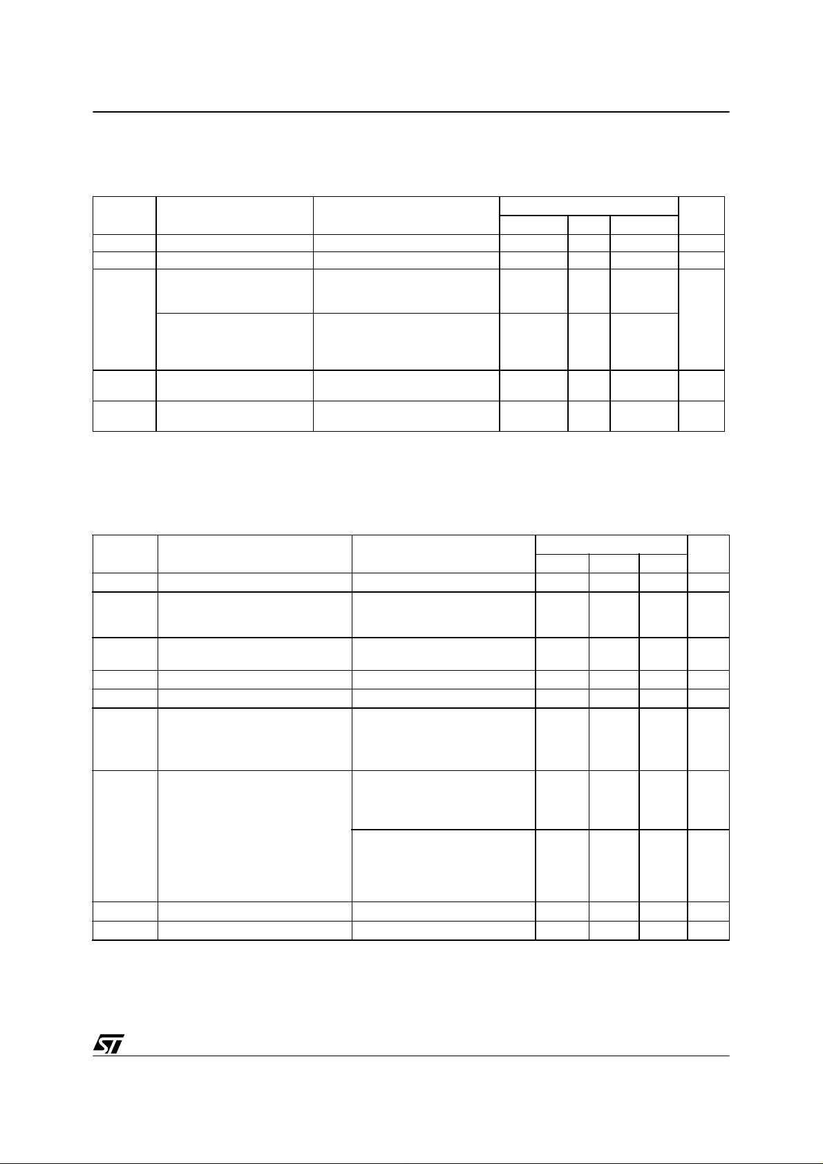
DC ELECTRICAL CHARACTERISTICS (Cont’d)
= -40 to +85°C unless otherwise specified))
(T
A
ST62T52C ST62T62C/E62C
Symbol Parameter Test Conditions
V
V
V
V
I
DD
Note:
(*) All Peripherals in stand-by.
LVD Threshold in power-on Vdn +50 mV 4.1 4.3 V
up
L VD threshold in powerdown 3.6 3.8 Vup -50 mV V
dn
V
Low Level Output Voltage
All Output pins
OL
Low Level Output Voltage
30 mA Sink I/O pins
High Level Output Voltage
OH
All Output pins
Supply Current in STOP
Mode, with LVD disabled
V
V
V
V
V
V
VDD= 5.0V; I
V
I
LOAD
(*)
V
= 5.0V; I
DD
= 5.0V; I
DD
= 5.0V; I
DD
= 5.0V; I
DD
= 5.0V; I
DD
= 5.0V; I
DD
= 5.0V; IOL = +30mA
DD
= 5.0V; I
DD
=0mA
=5.0V
DD
= +10µA
OL
= + 5mA
OL
= + 10mAv
OL
= +10µA
OL
= +10mA
OL
= +20mA
OL
= -10µA
OH
= -5.0mA
OH
6.4 AC ELECTRICAL CHARACTERISTICS
= -40 to +125°C unless otherwise specified)
(T
A
Symbol Parameter Test Conditions
t
REC
T
WEE
Endurance
(2)
Supply Recovery Time
EEPROM Write Time
EEPROM WRITE/ERASE Cycle QA LOT Acceptance (25°C) 300,000 1 million cycles
(1)
= 25°C
T
A
T
= 85°C
A
= 125°C
T
A
Value
Min. Typ. Max.
0.1
0.8
1.2
0.1
0.8
1.3
2.0
4.9
3.5
10 µA
Value
Min. Typ. Max.
100 ms
5
10
20
10
20
30
Unit
V
V
Unit
ms
Retention EEPROM Data Retention T
f
LFA O
f
OSG
Internal frequency with LFA O active 200 400 800 kHz
Internal Frequency with OSG
enabled
2)
= 55°C 10 years
A
V
= 3V
DD
= 3.6V
V
DD
= 4.5V
V
DD
V
= 6V
DD
VDD=5.0V (Except 626xB ROM)
R=47kΩ
R=100kΩ
f
RC
Internal frequency with RC oscillator and OSG disabled
2) 3)
R=470kΩ
VDD=5.0V (626xB ROM)
R=10kΩ
R=27kΩ
R=67kΩ
R=100kΩ
C
C
OUT
Notes:
1. Period for which V
2 An oscillator frequency above 1MHz is recommended for reliable A/D results.
3. Measure performed with OSCin pin soldered on PCB, with an around 2pF equivalent capacitance.
Input Capacitance All Inputs Pins 10 pF
IN
Output Capacitance All Outputs Pins 10 pF
has to be connected at 0V to all ow internal Reset funct i on at next power-up.
DD
1
1
2
2
4
2.7
800
6.3
4.7
2.8
2.2
5
3.2
850
8.2
5.9
3.6
2.8
f
OSC
5.8
3.5
900
9.8
4.3
3.4
MHz
MHz
MHz
kHz
MHz
7
MHz
MHz
MHz
61/78
Page 62

ST62T52C ST62T62C/E62C
6.5 A/D CONVERTER CHARACTERISTICS
(T
= -40 to +125°C unless otherwise specified)
A
Symbol Parameter Test Conditions
Min. Typ. Max.
Res Resolution 8 Bit
f
A
TOT
t
C
Total Accuracy
Conversion Time
(1) (2)
ZIR Zero Input Reading
FSR Full Scale Reading
AD
AC
Notes:
1. Noise at VDD, VSS <10 mV
2. With oscillator frequencie s less than 1MH z, the A/D Conver t er accuracy is decreased.
Analog Input Current During
I
Conversion
Analog Input Capacitan ce 2 5 pF
IN
> 1.2MHz
OSC
f
> 32kHz
OSC
f
= 8MHz (TA < 85°C)
OSC
f
= 4 MHz
OSC
Conversion result when
V
= V
IN
SS
00 Hex
Conversion result when
V
= V
IN
DD
V
= 4.5V 1.0 µA
DD
6.6 TIMER CHARACTERISTICS
Value
±2
±4
70
140
FF Hex
Unit
LSB
µs
= -40 to +125°C unless otherwise specified)
(T
A
Symbol Parameter Test Conditions
f
IN
t
W
Input Frequency on TIMER Pin MHz
V
= 3.0V
Pulse Width at TIMER Pin
V
DD
DD
>4.5V
6.7 SPI CHARACTERISTICS
(T
= -40 to +125°C unless otherwise specified)
A
Symbol Parameter Test Conditions
F
CL
t
SU
t
h
Clock Frequency Applied on Scl 500 kHz
Set-up Time Applied on Sin 250 ns
Hold Time Applied onSin 50 ns
6.8 ARTIMER ELECTRICAL CHARACTERISTICS
(T
= -40 to +125°C unless otherwise specified)
A
Symbol Parameter Test Conditions
Value
Min. Typ. Max.
1
125
Value
Min. Typ. Max.
Value
Min Typ Max
f
INT
--------- -
4
Unit
µs
ns
Unit
Unit
f
62/78
Input Frequency on ARTIMin Pin
IN
RUN and WAIT Modes
STOP mode 2
MHz
Page 63

Figure 31. Vol versus Iol on all I/O port at Vdd=5V
8
ST62T52C ST62T62C/E62C
6
4
Vol (V)
2
0
010203040
Iol (mA)
This curves represents typical variations and is given for guidance only
Figure 32. Vol versus Iol on all I/O port at T=25°C
8
6
4
Vol (V)
2
0
0 10203040
Iol (mA)
T = -40°C
T = 25°C
T = 95°C
T = 125°C
Vdd = 3.0V
Vdd = 4.0V
Vdd = 5.0V
Vdd = 6.0V
This curves represents typical variations and is given for guidance only
Figure 33. Vol versus Iol for High sink (30mA) I/Oport s at T=25°C
5
4
3
2
Vol (V)
1
0
0 10203040
Iol (mA)
This curves represents typical variations and is given for guidance only
Vdd = 3.0V
Vdd = 4.0V
Vdd = 5.0V
Vdd = 6.0V
63/78
Page 64

ST62T52C ST62T62C/E62C
Figure 34. Vol versus Iol for High sink (30mA) I/O ports at Vdd=5V
5
4
3
2
Vol (V)
1
0
0 10203040
Iol (mA)
This curves represents typical variations and is given for guidance only
Figure 35. Voh versus Ioh on all I/O port at 25°C
6
4
2
Voh (V)
0
-2
0 10203040
Ioh (mA)
T = -40°C
T = 25°C
T = 95°C
T = 125°C
Vdd = 3.0V
Vdd = 4.0V
Vdd = 5.0V
Vdd = 6.0V
This curves represents typical variations and is given for guidance only
Figure 36. Voh versus Ioh on all I/O por t at Vdd=5V
6
4
2
Voh (V)
0
-2
0 10203040
Ioh (mA)
This curves represents typical variations and is given for guidance only
64/78
T = -40°C
T = 25°C
T = 95°C
T = 125°C
Page 65

Figure 37. Idd W A I T ver sus VDD at 8 Mhz for OTP devices
2.5
2
1.5
1
0.5
Idd WAIT (mA)
0
3V 4V 5V 6V
Vdd
This curves represents typical variations and is given for guidance only
ST62T52C ST62T62C/E62C
T = -40°C
T = 25°C
T = 95°C
T = 125°C
Figure 38. Idd S TOP versus V
8
6
4
2
0
Idd STOP (µA)
-2
3V 4V 5V 6V
for OTP devices
DD
Vdd
This curves represents typical variations and is given for guidance only
Figure 39. Idd S TOP versus V
2
1.5
1
0.5
Idd STO P (µ A)
0
for ROM devices
DD
T = -40°C
T = 25°C
T = 95°C
T = 125°C
T = -40°C
T = 25°C
T = 95°C
T = 125°C
-0.5
3V 4V 5V 6V
Vdd
This curves represents typical variations and is given for guidance only
65/78
Page 66

ST62T52C ST62T62C/E62C
Figure 40. Idd W A I T ver sus VDD at 8Mhz for ROM devices
2.5
2
1.5
1
0.5
Idd WAIT (mA)
0
3V 4V 5V 6V
Vdd
This curves represents typical variations and is given for guidance only
Figure 41. Idd RUN versus V
8
6
4
Idd RUN ( mA)
2
0
3V 4V 5V 6V
at 8 Mhz for ROM and OTP devices
DD
Vdd
This curves represents typical variations and is given for guidance only
T = -40°C
T = 25°C
T = 95°C
T = 125°C
T = -40°C
T = 25°C
T = 95°C
T = 125°C
Figure 42. LVD thresholds versus temperature
4.2
4.1
4
3.9
Vthresh.
3.8
3.7
-40°C 25°C 95°C 125°C
Temp
This curves represents typical variations and is given for guidance only
66/78
Vup
Vdn
Page 67

Figure 43. RC frequency versus VDD for ROM ST626xB only
10
ST62T52C ST62T62C/E62C
R=1OK
R=27K
MHz
Frequency
1
3456
VDD (volts)]
This curves represents typical variations and is given for guidance only
Figure 44. RC frequency versus V
(Except for ST626xB ROM devices)
DD
10
1
MHz
Frequency
R=67K
R=100K
R=47K
R=100K
R=470K
0.1
3 3.5 4 4.5 5 5.5 6
VDD (vol t s)
This curves represents typical variations and is given for guidance only
67/78
Page 68

ST62T52C ST62T62C/E62C
7 GENERAL IN FORMATION
7.1 PACKAGE MECHANICAL DATA
Figure 45. 16-Pin Plastic Dual In-Line Package, 300-mil Width
E
A2
A
A1
L
D1
b3
b2
D
b
e
c
E1
eB
Figure 46. 16-Pin Ceramic Side-Brazed Dual In-Line Package
CDIP16W
Dim.
mm inches
Min Typ Max Min Typ Max
A 5.33 0.210
A1 0.38 0.015
A2 2.92 3.30 4.95 0.115 0.130 0.195
b 0.36 0.46 0.56 0.014 0.018 0.022
b2 1.14 1.52 1.78 0.045 0.060 0.070
b3 0.76 0.99 1.14 0.030 0.039 0.045
c 0.20 0.25 0.36 0.008 0.010 0.014
D 18.67 19.18 19.69 0.735 0.755 0.775
D1 0.13 0.005
e 2.54 0.100
E 7.62 7.87 8.26 0.300 0.310 0.325
E1 6.10 6.35 7.11 0.240 0.250 0.280
L 2.92 3.30 3.81 0.115 0.130 0.150
eB 10.92 0.430
Number of Pins
N 16
Dim.
mm inches
Min Typ Max Min Typ Max
A 3.78 0.149
A1 0.38 0.015
B 0.36 0.46 0.56 0.014 0.018 0.022
B1 1.14 1.37 1.78 0.045 0.054 0.070
C 0.20 0.25 0.36 0.008 0.010 0.014
D 19.86 20.32 20.78 0.782 0.800 0.818
D1 17.78 0.700
E1 7.04 7.49 7.95 0.277 0.295 0.313
e 2.54 0.100
G 6.35 6.60 6.86 0.250 0.260 0.270
G1 9.47 9.73 9.98 0.373 0.383 0.393
G2 1.02 0.040
L 2.92 3.30 3.81 0.115 0.130 0.150
S 1.27 0.050
Ø 4.22 0.166
Number of Pins
N16
68/78
Page 69

PACKAGE MECHANICAL DATA (Cont’d)
Figure 47. 16-Pin Plastic Small Outline Package, 300-mil Width
ST62T52C ST62T62C/E62C
D
L
A
A1
B
e
H
E
a
Figure 48. 16-Pin Plastic Shrink Small Outline Package
h x 45×
Dim.
A 2.35 2.65 0.093 0.104
C
mm inches
Min Typ Max Min Typ Max
A1 0.10 0.30 0.004 0.012
B 0.33 0.51 0.013 0.020
C 0.23 0.32 0.009 0.013
D 10.10 10.50 0.398 0.413
E 7.40 7.60 0.291 0.299
H 10.00 10.65 0.394 0.419
e 1.27 0.050
h 0.25 0.75 0.010 0.030
α 0° 8° 0° 8°
L 0.40 1.27 0.016 0.050
Number of Pins
N 16
D
A2
A
A1
b
e
L
h
Dim.
A 2.00 0.079
c
A1 0.05 0.002
A2 1.65 1.75 1.85 0.065 0.069 0.073
b 0.22 0.38 0.009 0.015
mm inches
Min Typ Max Min Typ Max
c 0.09 0.25 0.004 0.010
D 5.90 6.20 6.50 0.232 0.244 0.256
E 7.40 7.80 8.20 0.291 0.307 0.323
E1 5.00 5.30 5.60 0.197 0.209 0.220
E
E1
e 0.65 0.026
θ 0° 4° 8° 0° 4° 8°
L 0.55 0.75 0.95 0.022 0.030 0.037
Number of Pins
N 16
69/78
Page 70

ST62T52C ST62T62C/E62C
THERMAL CHARACTERISTIC
Symbol Parameter Test Conditions
RthJA Thermal Resistance
PDIP16 55
PSO16 75
Min. Typ. Max.
Value
7.2 ORDERING INFORMATION
Table 22. OTP/EPROM VERSION ORDERING INFORMATION
Sales Type
ST62E62CF1 1836 EPROM 64 0 to +70°C CDIP16W
ST62T52CM6
ST62T52CM3
ST62T62CM6
ST62T62CM3
ST62T52CB6
ST62T52CB3
ST62T62CB6
ST62T62CB3
ST62T52CN6
ST62T52CN3
ST62T62CN6
ST62T62CN3
Program
Memory (Bytes)
1836 OTP None
1836 OTP 64
1836 OTP None
1836 OTP 64
1836 OTP None
1836 OTP 64
EEPROM (Bytes) Temperature Range Package
-40 to + 85°C
-40 to + 125°C
-40 to + 85°C
-40 to + 125°C
-40 to + 85°C
-40 to + 125°C
-40 to + 85°C
-40 to + 125°C
-40 to + 85°C
-40 to + 125°C
-40 to + 85°C
-40 to + 125°C
PSO16
PSO16
PDIP16
PDIP16
SSOP16
SSOP16
Unit
°C/W
70/78
Page 71

8-BIT FAST ROM MCUs WITH A/D CONVERTER,
SAFE RESET, AUTO-RELOAD TIMER AND EEPROM
■ 3.0 to 6.0V Supply Operating Range
■ 8 MHz Maximum Clock Frequency
■ -40 to +125°C Operating Temperature Range
■ Run, Wait and Stop Modes
■ 5 Interrupt Vectors
■ Look-up Table capability in Program Memory
■ Data Storage in Program Memory:
User selectable size
■ Data RAM: 128 bytes
■ Data EEPROM: 64 bytes (none on ST 62T 5 2 C )
■ 9 I/O pins, fully programmable as:
– Input with pull-up resistor
– Input without pull-up resistor
– Input with interrupt generation
– Open-drain or push-pull output
– Analog Input
■ 5 I/O lines can sink up to 30mA to drive LEDs or
TRIACs directly
■ 8-bit Timer/Counter with 7-bit programmable
prescaler
■ 8-bit Auto-reload Timer with 7-bit programmable
prescaler (AR Timer)
■ Digital Watchdog
■ Oscillator Safe Guard
■ Low Voltage Detector for Safe Reset
■ 8-bit A/D Converter with 4 analog inputs
■ On-chip Clock oscillator can be driven by Quartz
Crystal Ceramic resonator or RC network
■ User configurable Power-on Reset
■ One external Non-Maskable Interrupt
■ ST626x-EMU2 Emulation and Development
System (connects to an MS-DOS PC via a
parallel port)
ST62P52C
ST62P62C
PDIP16
PSO16
SSOP16
(See end of Datasheet for Ordering Information)
DEVICE SUMMARY
DEVICE
ST62P52C 1836 ST62P62C 1836 64
ROM
(Bytes)
EEPROM
Rev. 3.0
February 2002 71/78
Page 72

ST62P52C ST62P62C
1 GENERAL DESCRIPTIO N
1.1 INTRODUCTION
The ST62P52C and ST62P62C are the Factory
Advanced Service Technique ROM (FASTROM)
version of ST62T52C and ST62T62C OTP devices.
They offer the same functionality as OTP devices,
selecting as FASTROM options the options defined in the program mab le o ption b yte of the OTP
version.
1.2.2 Listing Generation and Verification
When STMicroelectronics receives the user’s
ROM contents, a computer listing is generated
from it. This listing refers exactly to the ROM contents and options which will be used to produce
the specified MCU. The listing is then returned to
the customer who must thoroughly check, complete, sign and return it to STMicroelectronics. The
signed listing forms a part of the cont ractual agreement for the production of the specific customer
1.2 ORDERING INFORMATION
The following section deals with the procedure for
transfer of customer codes to STMicroelectronics.
1.2.1 Transfer of Customer Code
MCU.
The STMicroelectronics Sales Organization will be
pleased to provide detailed information on contractual points.
Customer code is made up of the RO M contents
and the list of the selected FASTROM options.
Table 23. ROM Memory Map ST62P52C/ P 62C
The ROM contents are to be sent on diskette, or
by electronic means, with the hexadecimal file
generated by the development tool. All unused
bytes must be set to FFh.
The selected options are com municated t o STM icroelectronics using the correctly filled OPTION
LIST appended. See page 76.
Device Address Description
0000h-087Fh
0880h-0F9Fh
0FA0h-0FEFh
0FF0h-0FF7h
0FF8h-0FFBh
0FFCh-0FFDh
0FFEh-0FFFh
Table 24. FASTROM version Orderi ng Information
Sales Type ROM EEPROM (Bytes) Temperature Range Package
ST62P52CM1/XXX
ST62P52CM6/XXX
ST62P52CM3/XXX (*)
ST62P62CM1/XXX
ST62P62CM6/XXX
ST62P62CM3/XXX (*)
ST62P52CB1/XXX
ST62P52CB6/XXX
ST62P52CB3/XXX (*)
ST62P62CB1/XXX
ST62P62CB6/XXX
ST62P62CB3/XXX (*)
ST62P52CN1/XXX
ST62P52CN6/XXX
ST62P52CN3/XXX (*)
ST62P62CN1/XXX
ST62P62CN6/XXX
ST62P62CN3/XXX (*)
1836 Bytes None
1836 Bytes 64
1836 Bytes None
1836 Bytes 64
1836 Bytes None
1836 Bytes 64
0 to +70°C
-40 to + 85°C
-40 to + 125°C
0 to +70°C
-40 to + 85°C
-40 to + 125°C
0 to +70°C
-40 to + 85°C
-40 to + 125°C
0 to +70°C
-40 to + 85°C
-40 to + 125°C
0 to +70°C
-40 to + 85°C
-40 to + 125°C
0 to +70°C
-40 to + 85°C
-40 to + 125°C
Reserved
User ROM
Reserved
Interrupt Vectors
Reserved
NMI Interrupt Vector
Reset Vector
PSO16
PDIP16
SSOP16
(*) Advanced information
72/78
Page 73

ST6252C
ST6262B
8-BIT ROM MCUs WITH A/D CONVERTER,
SAFE RESET AUTO-RELOAD TIMER, ROM AND EEPROM
■ 3.0 to 6.0V Supply Operating Range
■ 8 MHz Maximum Clock Frequency
■ -40 to +125°C Operating Temperature Range
■ Run, Wait and Stop Modes
■ 5 Interrupt Vectors
■ Look-up Table capability in Program Memory
■ Data Storage in Program Memory:
User selectable size
■ Data RAM: 128 bytes
■ Data EEPROM: 64 bytes (none on ST 62T 5 2 C )
■ 9 I/O pins, fully programmable as:
– Input with pull-up resistor
– Input without pull-up resistor
– Input with interrupt generation
– Open-drain or push-pull output
– Analog Input
■ 5 I/O lines can sink up to 30mA to drive LEDs or
TRIACs directly
■ 8-bit Timer/Counter with 7-bit programmable
prescaler
■ 8-bit Auto-reload Timer with 7-bit programmable
prescaler (AR Timer)
■ Digital Watchdog
■ Oscillator Safe Guard
■ Low Voltage Detector for Safe Reset
■ 8-bit A/D Converter with 4 analog inputs
■ On-chip Clock oscillator can be driven by Quartz
Crystal Ceramic resonator or RC network
■ User configurable Power-on Reset
■ One external Non-Maskable Interrupt
■ ST626x-EMU2 Emulation and Development
System (connects to an MS-DOS PC via a
parallel port)
(See end of Datasheet for Ordering Information)
PDIP16
PSO16
SSOP16
DEVICE SUMMARY
DEVICE
ST6252C 1836 - Y es
ST6262B 18 36 6 4 No
ROM
(Bytes)
EEPROM LVD & OSG
Rev. 3.0
February 2002 73/78
Page 74

ST6252C ST6262B
1 GENERAL DESCRIPTIO N
1.1 INTRODUCTION
The ST6252C and ST6262B are mask programmed ROM version of ST62T52C and
ST62T62C OTP devices.
Figure 1. Programming Waveform
TEST
15
14V typ
10
TEST
100mA
max
5
0.5s min
150 µs typ
They offer the same functionality as OTP devices,
selecting as ROM options the options def ined in
the programmable option byte of the OTP version,
except the LVD & OSG options that are not available on the ST6262B ROM device.
In case the user wants to blow this fuse, high voltage must be applied on the TEST pin.
Figure 2. Programming Circuit
5V
V
SS
V
DD
47mF
100nF
4mA typ
t
VR02001
1.2 ROM READOUT PROTECTION
If the ROM READOUT PROTECTION option is
selected, a protection fuse can be blo wn to prevent any access to the program memory content.
PROTECT
TEST
100nF
Note: ZPD 15 is used for overvoltage protection
ZPD15
15V
14V
VR02003
74/78
Page 75

ST6252C ST6262B
1.3 ORDERING INFORMATION
from it. This listing refers exactly to the mask which
will be used to produce the specified MCU. The
The following section deals with the procedure for
transfer of customer codes to STMicroelectronics.
1.3.1 Transfer of Customer Code
listing is then returned to the customer who must
thoroughly check, complet e, sign and return it to
STMicroelectronics. The signed listing forms a
part of the contractual agreement for the creat ion
Customer code is made up of the RO M contents
and the list of the selected mask options. The
ROM contents are to be sent on diskette, or by
electronic means, with the hexadecimal file generated by the development tool. All unused bytes
must be set to FFh.
The selected mask o ptions are communica ted to
STMicroelectronics using the correctly filled OPTION LIST appended. See page 76.
1.3.2 Listing Generation and V eri f icati on
When STMicroelectronics receives the user’s
ROM contents, a computer listing is generated
Table 26. ROM version Ordering Information
Sales Type ROM EEPROM (Bytes) Temperature Range Package
ST6252CB1/XXX
ST6252CB6/XXX
ST6252CB3/XXX
ST6252CM1/XXX
ST6252CM6/XXX
ST6252CM3/XXX
ST6252CN1/XXX
ST6252CN6/XXX
ST6252CN3/XXX
ST6262BB1/XXX
ST6262BB6/XXX
ST6262BB3/XXX
ST6262BM1/XXX
ST6262BM6/XXX
ST6262BM3/XXX
ST6262BN1/XXX
ST6262BN6/XXX
ST6262BN3/XXX
1836 Bytes None
1836 Bytes 64
of the specific customer mask.
The STMicroelectronics Sales Organization will be
pleased to provide detailed information on con-
tractual points.
Table 25. ROM Memory Map for ST6252 C/62B
Device Address Description
0000h-087Fh
0880h-0F9Fh
0FA0h-0FEFh
0FF0h-0FF7h
0FF8h-0FFBh
0FFCh-0FFDh
0FFEh-0FFFh
0 to +70°C
-40 to + 85°C
-40 to + 125°C
0 to +70°C
-40 to + 85°C
-40 to + 125°C
0 to +70°C
-40 to + 85°C
-40 to + 125°C
0 to +70°C
-40 to + 85°C
-40 to + 125°C
0 to +70°C
-40 to + 85°C
-40 to + 125°C
0 to +70°C
-40 to + 85°C
-40 to + 125°C
Reserved
User ROM
Reserved
Interrupt Vectors
Reserved
NMI Interrupt Vector
Reset Vector
PDIP16
PSO16
SSOP16
PDIP16
PSO16
SSOP16
75/78
Page 76

ST6252C ST6262B
ST6252C/62B/P52C/P62C MICROCONTROLLER OPTION LIST
Customer: . . . . . . . . . . . . . . . . . . . . . . . . . . . . . . . . . . . . . . . . . . . . . . . . . . . . . . . . . . . . . . . . . . . . . . . . . .
Address: . . . . . . . . . . . . . . . . . . . . . . . . . . . . . . . . . . . . . . . . . . . . . . . . . . . . . . . . . . . . . . . . . . . . . . . . . .
. . . . . . . . . . . . . . . . . . . . . . . . . . . . . . . . . . . . . . . . . . . . . . . . . . . . . . . . . . . . . . . . . . . . . . . . . .
Contact: . . . . . . . . . . . . . . . . . . . . . . . . . . . . . . . . . . . . . . . . . . . . . . . . . . . . . . . . . . . . . . . . . . . . . . . . . .
Phone: . . . . . . . . . . . . . . . . . . . . . . . . . . . . . . . . . . . . . . . . . . . . . . . . . . . . . . . . . . . . . . . . . . . . . . . . . .
Reference: . . . . . . . . . . . . . . . . . . . . . . . . . . . . . . . . . . . . . . . . . . . . . . . . . . . . . . . . . . . . . . . . . . . . . . . . . .
STMicroelectronics references:
Device: [ ] ST6252C (2 KB) [ ] ST6262B (2 KB)
Package: [ ] Dual in Line Plastic
Conditioning option: [ ] Standard (Tube) [ ] Tape & Reel
Temperature Range: [ ] 0°C to + 70°C [ ] - 40°C to + 85°C
Marking: [ ] Standard marking
Authorized characters are letters, digits, '.', '-', '/' and spaces only.
Oscillator Safeguard*: [ ] Enabled [ ] Disabled
Oscillator Selection: [ ] Quartz crystal / Ceramic resonator
Reset Delay: [ ] 32768 cycle delay [ ] 2048 cycle delay
Watchdog Selection: [ ] Software Activation [ ] Hardware Activation
PB3:PB2 pull-up at RESET*: [ ] Enabled [ ] Disabled
External STOP Mode Control: [ ] Enabled [ ] Disabled
Readout Protection: F ASTR OM:
ROM:
[ ] Fuse is blown by STMicroelectronics
[ ] Fuse can be blown by the customer
[ ] ST62P52C (2 KB) [ ] ST62P62C (2 KB)
[ ] Small Outline Plastic with conditioning
[ ] Shrink Small Outline Plastic with conditioning
[ ] - 40°C to + 125°C
[ ] Special marking (ROM only):
[ ] RC network
[ ] Enabled [ ] Disabled
[ ] Enabled:
[ ] Disabled
PDIP16 (9 char. max): _ _ _ _ _ _ _ _ _
PSO16 (6 char. max): _ _ _ _ _ _
SSOP16 (10 char. max): _ _ _ _ _ _ _ _ _ _
Low Voltage Detector*: [ ] Enabled [ ] Disabled
NMI pull-up*: [ ] Enabled [ ] Disabled
ADC Synchro*: [ ] Enabled [ ] Disabled
*except on ST6262B
Comments:
Oscillator Frequency in the application: . . . . . . . . . . . . . . . . . . . . . . . . . . . . . . . . . . . . . . . . . . . . .
Supply Operating Range in the application: . . . . . . . . . . . . . . . . . . . . . . . . . . . . . . . . . . . . . . . . . . . . .
Notes: . . . . . . . . . . . . . . . . . . . . . . . . . . . . . . . . . . . . . . . . . . . . . . . . . . . . . . . . . . . . . . . . . . . . . . . . . .
Date: . . . . . . . . . . . . . . . . . . . . . . . . . . . . . . . . . . . . . . . . . . . . . . . . . . . . . . . . . . . . . . . . . . . . . . . . . .
Signature: . . . . . . . . . . . . . . . . . . . . . . . . . . . . . . . . . . . . . . . . . . . . . . . . . . . . . . . . . . . . . . . . . . . . . . . . . .
76/78
Page 77

ST6252C ST6262B
2 SUMMAR Y OF CHANGES
Rev. Main Changes Date
Modification of “Additional Notes for EEPROM Parallel Mode” (p.13)
Changed f
In section 4.2 on page 41: vector #4 instead of vector #3 for the timer interrupt request.
2.9
Changed Figure 43 on page 67.
Changed Figure 45. on page 68 and Figure 47.and Figure 48. on page 69.
Changed option list on page 76.
Swapped D11 and D10 description on page 14:
D11. Reserved, must be cleared.
3.0
D10. Reserved, must be set to one.
values in section 6.4 on page 61
RC
July 2001
Feb 2002
77/78
Page 78

ST6252C ST6262B
Notes:
Information furnished is believed to be accurate and reliable. However, STMicroelectronics assumes no responsibility for the consequences
of use of such information nor for any infringement of patents or other rights of third parties which may result from its use. No license is granted
by implic ation or otherwise under any pat ent or pat ent rights of STMicroe l ectronics . Specificat i ons menti oned in thi s publication are subject
to change without notice. This publication supersedes and replaces all information previously supplied. STMicroelectronics products are not
authorized for use as cri t i cal compone nts in life support device s or systems without the express writt en approval of STMicroel ectronics.
The ST logo is a registered trademark of STMicroelectronics
2002 STMicroelectronics - All Rights Reserved.
STMicroelectronics Group of Compani es
http://www.s t. com
Purchase of I
2
C Components by STMicroelectronics conveys a license under the Philips I2C Patent. Rights to use the se component s i n an
2
C system i s granted pro vided that the system con forms to the I2C Standard Specification as defined by Philips.
I
Australi a - B razil - Canada - China - Finland - Franc e - Germany - Hong Kong - Ind i a - Israel - Ita l y - J apan
Malaysi a - M al ta - Morocco - Singapore - Spain - Sweden - Switz erland - Unit ed Kingdo m - U. S. A.
78/78
 Loading...