

Page 1

ST6215C/ST6225C
8-BIT MCUs WITH A/D CONVERTER,
TWO TIMERS, OSCILLATOR SAFEGUARD & SAFE RESET
■ Memories
– 2K or 4K bytes Program memory (OTP,
EPROM, FASTROM or ROM) with read-out
protection
– 64 bytes RAM
■ Clock, Re set and Supply M a nagement
– Enhanced reset system
– Low Voltage Detector (LVD) for Safe Reset
– Clock sources: crystal/ceramic resonator or
RC netwo rk, ex tern al cloc k, bac kup o scillat or
(LFAO)
– Oscillator Safeguard (OSG)
– 2 Power Saving Modes: Wait and Stop
■ Interrupt Management
– 4 interrupt vectors plus NMI and RESET
– 20 external interrupt lines (on 2 vectors)
– 1 external non-interrupt line
■ 20 I/ O P o rts
– 20 multifunctional bidirectional I/O lines
– 16 alternate function lines
– 4 high sink outputs (20mA)
■ 2 Timers
– Configurable watchdog timer
– 8-bit timer/counter with a 7-bit prescaler
■ Analog Peripheral
– 8-bit ADC with 16 input channels
■ Instructio n Set
– 8-bit data manipulation
– 40 basic instructions
– 9 addressing modes
– Bit manipulation
(See Section 12.5 for Ordering Information)
■ Development Tools
– Full hardware/software development package
PDIP28
S028
SS0P28
CDIP28W
Device Summary
Features
Program memory - bytes 2K 4K
RAM - byte s 64
Operati ng S upply 3.0V to 6V
Clock Fre quency 8MHz Max
Operating Temperature -40°C to +125°C
Packages PDIP28 / SO 28 / SSOP28 CDIP28 W
ST62T15C(OTP)
ST6215C(ROM)
ST62P15C(FASTROM)
ST62T25C(OTP)
ST6225C(ROM)
ST62P25C(FASTROM
ST62E25C(EPROM)
Rev. 3.3
October 2003 1/105
1
Page 2

Table of Contents
ST6215 C/ ST6225C . . . . . . . . . . . . . . . . . . . . . . . . . . . . . . . . . . . 1
1 INTRODUCTION . . . . . . . . . . . . . . . . . . . . . . . . . . . . . . . . . . . . . . . . . . . . . . . . . . . . . . . . . . . . . . 6
2 PIN DESCRIPTION . . . . . . . . . . . . . . . . . . . . . . . . . . . . . . . . . . . . . . . . . . . . . . . . . . . . . . . . . . . . 7
3 MEMORY MAPS, PROGRAMMING MODES AND OPTION BYTES . . . . . . . . . . . . . . . . . . . . . . 9
3.1 MEMORY AND REGISTER MAPS . . . . . . . . . . . . . . . . . . . . . . . . . . . . . . . . . . . . . . . . . . 9
3.1.1 Introduction . . . . . . . . . . . . . . . . . . . . . . . . . . . . . . . . . . . . . . . . . . . . . . . . . . . . . . . . 9
3.1.2 Program Space . . . . . . . . . . . . . . . . . . . . . . . . . . . . . . . . . . . . . . . . . . . . . . . . . . . . 11
3.1.3 Readout Protection . . . . . . . . . . . . . . . . . . . . . . . . . . . . . . . . . . . . . . . . . . . . . . . . . 11
3.1.4 Data Space . . . . . . . . . . . . . . . . . . . . . . . . . . . . . . . . . . . . . . . . . . . . . . . . . . . . . . . 11
3.1.5 Stack Space . . . . . . . . . . . . . . . . . . . . . . . . . . . . . . . . . . . . . . . . . . . . . . . . . . . . . . . 11
3.1.6 Data ROM Window Mechanis m . . . . . . . . . . . . . . . . . . . . . . . . . . . . . . . . . . . . . . . . 13
3.2 PROGRAMMING MODES . . . . . . . . . . . . . . . . . . . . . . . . . . . . . . . . . . . . . . . . . . . . . . . . 15
3.2.1 Program Memory . . . . . . . . . . . . . . . . . . . . . . . . . . . . . . . . . . . . . . . . . . . . . . . . . . . 15
3.2.2 EPROM Erasing . . . . . . . . . . . . . . . . . . . . . . . . . . . . . . . . . . . . . . . . . . . . . . . . . . . . 15
3.3 OPTION BYTES . . . . . . . . . . . . . . . . . . . . . . . . . . . . . . . . . . . . . . . . . . . . . . . . . . . . . . . 16
4 CENTRAL PROCESSING UNIT . . . . . . . . . . . . . . . . . . . . . . . . . . . . . . . . . . . . . . . . . . . . . . . . . 17
4.1 INTRODUCTION . . . . . . . . . . . . . . . . . . . . . . . . . . . . . . . . . . . . . . . . . . . . . . . . . . . . . . . 17
4.2 MAIN FEATURES . . . . . . . . . . . . . . . . . . . . . . . . . . . . . . . . . . . . . . . . . . . . . . . . . . . . . . 17
4.3 CPU REGISTERS . . . . . . . . . . . . . . . . . . . . . . . . . . . . . . . . . . . . . . . . . . . . . . . . . . . . . . 17
5 CLOCKS, SUPPLY AND RESET . . . . . . . . . . . . . . . . . . . . . . . . . . . . . . . . . . . . . . . . . . . . . . . . 19
5.1 CLOCK SYSTEM . . . . . . . . . . . . . . . . . . . . . . . . . . . . . . . . . . . . . . . . . . . . . . . . . . . . . . . 19
5.1.1 Main Oscillator . . . . . . . . . . . . . . . . . . . . . . . . . . . . . . . . . . . . . . . . . . . . . . . . . . . . . 20
5.1.2 Oscillator Safeguard (OSG) . . . . . . . . . . . . . . . . . . . . . . . . . . . . . . . . . . . . . . . . . . . 21
5.1.3 Low Frequenc y Au xiliar y Os c illa tor ( LFA O) . . . . . . . . . . . . . . . . . . . . . . . . . . . . . . . 22
5.1.4 Register Description . . . . . . . . . . . . . . . . . . . . . . . . . . . . . . . . . . . . . . . . . . . . . . . . . 22
5.2 LOW VOLTAGE DETECTOR (LVD) . . . . . . . . . . . . . . . . . . . . . . . . . . . . . . . . . . . . . . . . 23
5.3 RESET . . . . . . . . . . . . . . . . . . . . . . . . . . . . . . . . . . . . . . . . . . . . . . . . . . . . . . . . . . . . . . . 24
5.3.1 Introduction . . . . . . . . . . . . . . . . . . . . . . . . . . . . . . . . . . . . . . . . . . . . . . . . . . . . . . . 24
5.3.2 RESET Sequence . . . . . . . . . . . . . . . . . . . . . . . . . . . . . . . . . . . . . . . . . . . . . . . . . . 24
5.3.3 RESET
5.3.4 Watchdog Reset . . . . . . . . . . . . . . . . . . . . . . . . . . . . . . . . . . . . . . . . . . . . . . . . . . . 26
5.3.5 LVD Reset . . . . . . . . . . . . . . . . . . . . . . . . . . . . . . . . . . . . . . . . . . . . . . . . . . . . . . . . 26
6 INTERRUPTS . . . . . . . . . . . . . . . . . . . . . . . . . . . . . . . . . . . . . . . . . . . . . . . . . . . . . . . . . . . . . . . 27
6.1 INTERRUPT RULES AND PRIORITY MANAGEMENT . . . . . . . . . . . . . . . . . . . . . . . . . 29
6.2 INTERRUPTS AND LOW POWER MODES . . . . . . . . . . . . . . . . . . . . . . . . . . . . . . . . . . 29
6.3 NON MASKABLE INTERRUPT . . . . . . . . . . . . . . . . . . . . . . . . . . . . . . . . . . . . . . . . . . . . 29
6.4 PERIPHERAL INTERRUPTS . . . . . . . . . . . . . . . . . . . . . . . . . . . . . . . . . . . . . . . . . . . . . 29
6.5 EXTERNAL INTERRUPTS (I/O PORTS) . . . . . . . . . . . . . . . . . . . . . . . . . . . . . . . . . . . . 30
6.5.1 Notes on using External Interrupts . . . . . . . . . . . . . . . . . . . . . . . . . . . . . . . . . . . . . . 30
6.6 INTERRUPT HANDLING PROCEDURE . . . . . . . . . . . . . . . . . . . . . . . . . . . . . . . . . . . . . 31
6.6.1 Interrupt Response Time . . . . . . . . . . . . . . . . . . . . . . . . . . . . . . . . . . . . . . . . . . . . . 31
6.7 REGISTER DESCRIPTION . . . . . . . . . . . . . . . . . . . . . . . . . . . . . . . . . . . . . . . . . . . . . . . 32
Pin . . . . . . . . . . . . . . . . . . . . . . . . . . . . . . . . . . . . . . . . . . . . . . . . . . . . . . . . 25
105
2/105
2
Page 3

Table of Contents
7 POWER SAVING MODES . . . . . . . . . . . . . . . . . . . . . . . . . . . . . . . . . . . . . . . . . . . . . . . . . . . . . 33
7.1 INTRODUCTION . . . . . . . . . . . . . . . . . . . . . . . . . . . . . . . . . . . . . . . . . . . . . . . . . . . . . . . 33
7.2 WAIT MODE . . . . . . . . . . . . . . . . . . . . . . . . . . . . . . . . . . . . . . . . . . . . . . . . . . . . . . . . . . 34
7.3 STOP MODE . . . . . . . . . . . . . . . . . . . . . . . . . . . . . . . . . . . . . . . . . . . . . . . . . . . . . . . . . . 35
7.4 NOTES RELATED TO WAIT AND STOP MODES . . . . . . . . . . . . . . . . . . . . . . . . . . . . . 37
7.4.1 Exit from Wait and Stop Modes . . . . . . . . . . . . . . . . . . . . . . . . . . . . . . . . . . . . . . . . 37
7.4.2 Recommende d MCU Configuration . . . . . . . . . . . . . . . . . . . . . . . . . . . . . . . . . . . . . 37
8 I/O PORTS . . . . . . . . . . . . . . . . . . . . . . . . . . . . . . . . . . . . . . . . . . . . . . . . . . . . . . . . . . . . . . . . . . 3 8
8.1 INTRODUCTION . . . . . . . . . . . . . . . . . . . . . . . . . . . . . . . . . . . . . . . . . . . . . . . . . . . . . . . 38
8.2 FUNCTIONAL DESCRIPTION . . . . . . . . . . . . . . . . . . . . . . . . . . . . . . . . . . . . . . . . . . . . 38
8.2.1 Digital Input Modes . . . . . . . . . . . . . . . . . . . . . . . . . . . . . . . . . . . . . . . . . . . . . . . . . 38
8.2.2 Analog Inputs . . . . . . . . . . . . . . . . . . . . . . . . . . . . . . . . . . . . . . . . . . . . . . . . . . . . . . 38
8.2.3 Output Modes . . . . . . . . . . . . . . . . . . . . . . . . . . . . . . . . . . . . . . . . . . . . . . . . . . . . . 38
8.2.4 Alternate Functions . . . . . . . . . . . . . . . . . . . . . . . . . . . . . . . . . . . . . . . . . . . . . . . . . 38
8.2.5 Instructions NOT to be used to access Port Data registers (SET, RES, INC and DEC) 40
8.2.6 Recommendations . . . . . . . . . . . . . . . . . . . . . . . . . . . . . . . . . . . . . . . . . . . . . . . . . . 40
8.3 LOW POWER MODES . . . . . . . . . . . . . . . . . . . . . . . . . . . . . . . . . . . . . . . . . . . . . . . . . . 40
8.4 INTERRUPTS . . . . . . . . . . . . . . . . . . . . . . . . . . . . . . . . . . . . . . . . . . . . . . . . . . . . . . . . . 40
8.5 REGISTER DESCRIPTION . . . . . . . . . . . . . . . . . . . . . . . . . . . . . . . . . . . . . . . . . . . . . . . 42
9 ON-CHIP PERIPHERALS . . . . . . . . . . . . . . . . . . . . . . . . . . . . . . . . . . . . . . . . . . . . . . . . . . . . . . 43
9.1 WATCHDOG TIMER (WDG) . . . . . . . . . . . . . . . . . . . . . . . . . . . . . . . . . . . . . . . . . . . . . . 43
9.1.1 Introduction . . . . . . . . . . . . . . . . . . . . . . . . . . . . . . . . . . . . . . . . . . . . . . . . . . . . . . . 43
9.1.2 Main Features . . . . . . . . . . . . . . . . . . . . . . . . . . . . . . . . . . . . . . . . . . . . . . . . . . . . . 43
9.1.3 Functional Description . . . . . . . . . . . . . . . . . . . . . . . . . . . . . . . . . . . . . . . . . . . . . . . 44
9.1.4 Recommendations . . . . . . . . . . . . . . . . . . . . . . . . . . . . . . . . . . . . . . . . . . . . . . . . . . 44
9.1.5 Low Power Modes . . . . . . . . . . . . . . . . . . . . . . . . . . . . . . . . . . . . . . . . . . . . . . . . . . 45
9.1.6 Interrupts . . . . . . . . . . . . . . . . . . . . . . . . . . . . . . . . . . . . . . . . . . . . . . . . . . . . . . . . . 45
9.1.7 Register Description . . . . . . . . . . . . . . . . . . . . . . . . . . . . . . . . . . . . . . . . . . . . . . . . . 46
9.2 8-BIT TIMER . . . . . . . . . . . . . . . . . . . . . . . . . . . . . . . . . . . . . . . . . . . . . . . . . . . . . . . . . . 47
9.2.1 Introduction . . . . . . . . . . . . . . . . . . . . . . . . . . . . . . . . . . . . . . . . . . . . . . . . . . . . . . . 47
9.2.2 Main Features . . . . . . . . . . . . . . . . . . . . . . . . . . . . . . . . . . . . . . . . . . . . . . . . . . . . . 47
9.2.3 Counter/Prescaler Description . . . . . . . . . . . . . . . . . . . . . . . . . . . . . . . . . . . . . . . . . 48
9.2.4 Functional Description . . . . . . . . . . . . . . . . . . . . . . . . . . . . . . . . . . . . . . . . . . . . . . . 49
9.2.5 Low Power Modes . . . . . . . . . . . . . . . . . . . . . . . . . . . . . . . . . . . . . . . . . . . . . . . . . . 51
9.2.6 Interrupts . . . . . . . . . . . . . . . . . . . . . . . . . . . . . . . . . . . . . . . . . . . . . . . . . . . . . . . . . 51
9.2.7 Register Description . . . . . . . . . . . . . . . . . . . . . . . . . . . . . . . . . . . . . . . . . . . . . . . . . 52
9.3 A/D CONVERTER (ADC) . . . . . . . . . . . . . . . . . . . . . . . . . . . . . . . . . . . . . . . . . . . . . . . . 53
9.3.1 Introduction . . . . . . . . . . . . . . . . . . . . . . . . . . . . . . . . . . . . . . . . . . . . . . . . . . . . . . . 53
9.3.2 Main Features . . . . . . . . . . . . . . . . . . . . . . . . . . . . . . . . . . . . . . . . . . . . . . . . . . . . . 53
9.3.3 Functional Description . . . . . . . . . . . . . . . . . . . . . . . . . . . . . . . . . . . . . . . . . . . . . . . 54
9.3.4 Recommendations . . . . . . . . . . . . . . . . . . . . . . . . . . . . . . . . . . . . . . . . . . . . . . . . . . 55
9.3.5 Low Power Modes . . . . . . . . . . . . . . . . . . . . . . . . . . . . . . . . . . . . . . . . . . . . . . . . . . 56
9.3.6 Interrupts . . . . . . . . . . . . . . . . . . . . . . . . . . . . . . . . . . . . . . . . . . . . . . . . . . . . . . . . . 56
9.3.7 Register Description . . . . . . . . . . . . . . . . . . . . . . . . . . . . . . . . . . . . . . . . . . . . . . . . . 56
10 INSTRUCTION SET . . . . . . . . . . . . . . . . . . . . . . . . . . . . . . . . . . . . . . . . . . . . . . . . . . . . . . . . . 57
3/105
3
Page 4

Table of Contents
10.1 ST6 ARCHITECTURE . . . . . . . . . . . . . . . . . . . . . . . . . . . . . . . . . . . . . . . . . . . . . . . . . . . 57
10.2 ADDRESSING MODES . . . . . . . . . . . . . . . . . . . . . . . . . . . . . . . . . . . . . . . . . . . . . . . . . . 57
10.3 INSTRUCTION SET . . . . . . . . . . . . . . . . . . . . . . . . . . . . . . . . . . . . . . . . . . . . . . . . . . . . 58
11 ELECTRICAL CHARACTERISTICS . . . . . . . . . . . . . . . . . . . . . . . . . . . . . . . . . . . . . . . . . . . . . 63
11.1 PARAMETER CONDITIONS . . . . . . . . . . . . . . . . . . . . . . . . . . . . . . . . . . . . . . . . . . . . . . 63
11.1.1Minimum and Maximum V alues . . . . . . . . . . . . . . . . . . . . . . . . . . . . . . . . . . . . . . . . 63
11.1.2Typical Values . . . . . . . . . . . . . . . . . . . . . . . . . . . . . . . . . . . . . . . . . . . . . . . . . . . . . 63
11.1.3Typical Curves . . . . . . . . . . . . . . . . . . . . . . . . . . . . . . . . . . . . . . . . . . . . . . . . . . . . . 63
11.1.4Loading Capacitor . . . . . . . . . . . . . . . . . . . . . . . . . . . . . . . . . . . . . . . . . . . . . . . . . . 63
11.1.5Pin Input Voltage . . . . . . . . . . . . . . . . . . . . . . . . . . . . . . . . . . . . . . . . . . . . . . . . . . . 63
11.2 ABSOLUTE MAXIMUM RATINGS . . . . . . . . . . . . . . . . . . . . . . . . . . . . . . . . . . . . . . . . . 64
11.2.1Voltage Characteristics . . . . . . . . . . . . . . . . . . . . . . . . . . . . . . . . . . . . . . . . . . . . . . 64
11.2.2Current Characteristics . . . . . . . . . . . . . . . . . . . . . . . . . . . . . . . . . . . . . . . . . . . . . . 64
11.2.3Thermal Characteristics . . . . . . . . . . . . . . . . . . . . . . . . . . . . . . . . . . . . . . . . . . . . . 64
11.3 OPERATING CONDITIONS . . . . . . . . . . . . . . . . . . . . . . . . . . . . . . . . . . . . . . . . . . . . . . 65
11.3.1General Operating Conditions . . . . . . . . . . . . . . . . . . . . . . . . . . . . . . . . . . . . . . . . 65
11.3.2Operating Conditions with Low Voltage Detector (LVD) . . . . . . . . . . . . . . . . . . . . . 66
11.4 SUPPLY CURRENT CHARACTERISTICS . . . . . . . . . . . . . . . . . . . . . . . . . . . . . . . . . . . 67
11.4.1 RUN Modes . . . . . . . . . . . . . . . . . . . . . . . . . . . . . . . . . . . . . . . . . . . . . . . . . . . . . . 67
11.4.2WAIT Modes . . . . . . . . . . . . . . . . . . . . . . . . . . . . . . . . . . . . . . . . . . . . . . . . . . . . . . 68
11.4.3STOP Mode . . . . . . . . . . . . . . . . . . . . . . . . . . . . . . . . . . . . . . . . . . . . . . . . . . . . . . 71
11.4.4Supply and Clock System . . . . . . . . . . . . . . . . . . . . . . . . . . . . . . . . . . . . . . . . . . . . 72
11.4.5On-Chip Peripherals . . . . . . . . . . . . . . . . . . . . . . . . . . . . . . . . . . . . . . . . . . . . . . . . 72
11.5 CLOCK AND TIMING CHARACTERISTICS . . . . . . . . . . . . . . . . . . . . . . . . . . . . . . . . . . 73
11.5.1General Timings . . . . . . . . . . . . . . . . . . . . . . . . . . . . . . . . . . . . . . . . . . . . . . . . . . . 73
11.5.2External Clock Source . . . . . . . . . . . . . . . . . . . . . . . . . . . . . . . . . . . . . . . . . . . . . . . 73
11.5.3Crystal and Ceramic Resonator Oscillators . . . . . . . . . . . . . . . . . . . . . . . . . . . . . . . 74
11.5.4RC Oscillator . . . . . . . . . . . . . . . . . . . . . . . . . . . . . . . . . . . . . . . . . . . . . . . . . . . . . . 75
11.5.5Oscillator Safeguard (OSG) and Low Frequency Auxiliary Oscillator (LFAO) . . . . . 76
11.6 MEMORY CHARACTERISTICS . . . . . . . . . . . . . . . . . . . . . . . . . . . . . . . . . . . . . . . . . . . 77
11.6.1RAM and Hardware Registers . . . . . . . . . . . . . . . . . . . . . . . . . . . . . . . . . . . . . . . . 77
11.6.2EPROM Program Memory . . . . . . . . . . . . . . . . . . . . . . . . . . . . . . . . . . . . . . . . . . . 77
11.7 EMC CHARACTERISTICS . . . . . . . . . . . . . . . . . . . . . . . . . . . . . . . . . . . . . . . . . . . . . . . 78
11.7.1Functional EMS . . . . . . . . . . . . . . . . . . . . . . . . . . . . . . . . . . . . . . . . . . . . . . . . . . . . 78
11.7.2Absolute Electrical Sensitivity . . . . . . . . . . . . . . . . . . . . . . . . . . . . . . . . . . . . . . . . . 79
11.7.3ESD Pin Protection Strategy . . . . . . . . . . . . . . . . . . . . . . . . . . . . . . . . . . . . . . . . . . 81
11.8 I/O PORT PIN CHARACTERISTICS . . . . . . . . . . . . . . . . . . . . . . . . . . . . . . . . . . . . . . . . 82
11.8.1General Characteristics . . . . . . . . . . . . . . . . . . . . . . . . . . . . . . . . . . . . . . . . . . . . . . 82
11.8.2Output Driving Current . . . . . . . . . . . . . . . . . . . . . . . . . . . . . . . . . . . . . . . . . . . . . . . 83
11.9 CONTROL PIN CHARACTERISTICS . . . . . . . . . . . . . . . . . . . . . . . . . . . . . . . . . . . . . . . 86
11.9.1Asynchronous RESET Pin . . . . . . . . . . . . . . . . . . . . . . . . . . . . . . . . . . . . . . . . . . . . 86
11.9.2NMI Pin . . . . . . . . . . . . . . . . . . . . . . . . . . . . . . . . . . . . . . . . . . . . . . . . . . . . . . . . . . 87
11.10 TIMER PERIPHERAL CHARACTERISTICS . . . . . . . . . . . . . . . . . . . . . . . . . . . . . . . . . . 88
11.10.1Watchdog Timer . . . . . . . . . . . . . . . . . . . . . . . . . . . . . . . . . . . . . . . . . . . . . . . . . . 88
11.10.28-Bit Timer . . . . . . . . . . . . . . . . . . . . . . . . . . . . . . . . . . . . . . . . . . . . . . . . . . . . . . . 88
11.11 8-BIT ADC CHARACTERISTICS . . . . . . . . . . . . . . . . . . . . . . . . . . . . . . . . . . . . . . . . . . 89
105
4/105
1
Page 5

Table of Contents
12 GENERAL INFORMATION . . . . . . . . . . . . . . . . . . . . . . . . . . . . . . . . . . . . . . . . . . . . . . . . . . . . 91
12.1 PACKAGE MECHANICAL DATA . . . . . . . . . . . . . . . . . . . . . . . . . . . . . . . . . . . . . . . . . . 91
12.2 THERMAL CHARACTERISTICS . . . . . . . . . . . . . . . . . . . . . . . . . . . . . . . . . . . . . . . . . . 93
12.3 SOLDERING AND GLUEABILITY INFORMATION . . . . . . . . . . . . . . . . . . . . . . . . . . . . . 94
12.4 PACKAGE/SOCKET FOOTPRINT PROPOSAL . . . . . . . . . . . . . . . . . . . . . . . . . . . . . . . 95
12.5 ORDERING INFORMATION . . . . . . . . . . . . . . . . . . . . . . . . . . . . . . . . . . . . . . . . . . . . . . 96
12.6 TRANSFER OF CUSTOMER CODE . . . . . . . . . . . . . . . . . . . . . . . . . . . . . . . . . . . . . . . 97
12.6.1FASTROM Version . . . . . . . . . . . . . . . . . . . . . . . . . . . . . . . . . . . . . . . . . . . . . . . . . 97
12.6.2ROM Version . . . . . . . . . . . . . . . . . . . . . . . . . . . . . . . . . . . . . . . . . . . . . . . . . . . . . . 98
13 DEVELOPMENT TOOLS . . . . . . . . . . . . . . . . . . . . . . . . . . . . . . . . . . . . . . . . . . . . . . . . . . . . 100
14 ST6 APPLICATION NOTES . . . . . . . . . . . . . . . . . . . . . . . . . . . . . . . . . . . . . . . . . . . . . . . . . . 102
15 SUMMARY OF CHANGES . . . . . . . . . . . . . . . . . . . . . . . . . . . . . . . . . . . . . . . . . . . . . . . . . . . 104
16 TO GET MORE INFORMATION . . . . . . . . . . . . . . . . . . . . . . . . . . . . . . . . . . . . . . . . . . . . . . . 104
5/105
1
Page 6

ST6215C/ST6225C
1 INTRODUCTION
The ST6215C, 25C devices are low cost members
of the ST62xx 8-bit HCMOS family of microcontrollers, which is targeted at low to medium complexity
applications. All ST62xx devices are based on a
building block approach: a common core is surrounded by a number of on-chip peripherals.
The ST62E25C is the erasable EPROM version of
the ST62T15C, T25C devices, which may be used
during the development phase for the ST62T15C,
T25C target devices, as well as the respective
ST6215C, 25C ROM devices.
OTP and EPROM devices are functional ly identical. OTP devices offer a ll the advantages of us er
programmability at low cost, which make them the
ideal choice in a wide range of applications where
frequent code changes, multiple c ode vers ions or
last minute programmabilit y are required.
The ROM based versions offer the same functionality, selecting the options defined in the program-
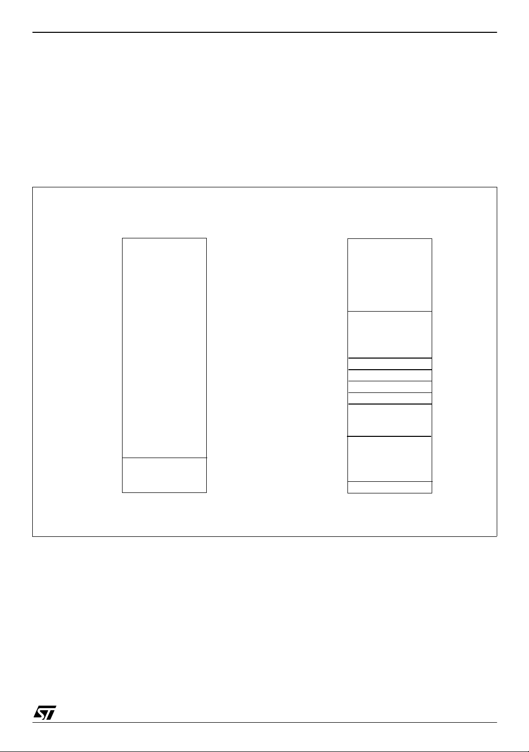
Figure 1. Block Diagram
8-BIT
A/D CONVERTER
V
PP
NMI
INTERR UPTS
mable option bytes of the OTP/EPR OM versions
in the ROM option list (See Section 12.6 on page
97).
The ST62P15C/P2 5C are the Factory Advanced
Service Technique ROM (FASTROM) versions of
ST62T15C,T25C OTP devices.
They offer the same functionality as OTP devices,
but they do not have to be programmed by the
customer (See Section 12 on page 91).
These compact low -cost devices feature a Timer
comprising an 8-bit counter with a 7-bit programmable prescaler, an 8-bit A/D Converter with 16
analog inputs and a Digital Wa tchdog timer, making them well suited for a wide range of automotive, appliance and industrial applications.
For easy reference, all parametric data is locat ed
in Section 11 on page 63.
PORT A
PORT B
PORT C
PA0..PA3 (20mA Sink)
PA4..PA7 / Ain
PB0..PB7 / Ain
PC4..PC7 / Ain
6/105
4
PROGRAM
:
MEMORY
(2K or 4K Bytes)
PC
STACK LEVEL 1
STACK LEVEL 2
STACK LEVEL 3
STACK LEVEL 4
STACK LEVEL 5
STACK LEVEL 6
POWER
SUPPLY
V
DDVSS
OSCILLATOR
OSCin OSCout RESET
DATA RO M
USER
SELECTABLE
DATA RAM
64 Bytes
8-BIT CO RE
RESET
TIMER
WATCHDOG
TIMER
TIMER
Page 7

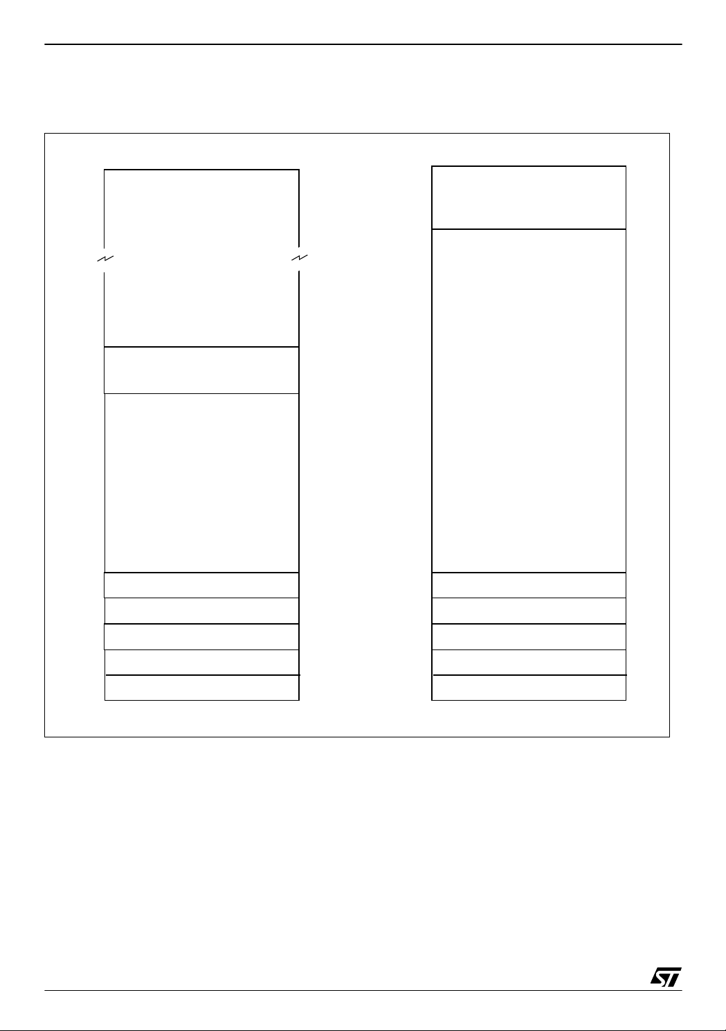
2 PIN DESCRI PTION
Figure 2. 28-Pin Package Pinout
ST6215C/ST6225C
Table 1. Device Pin Description
Pin n° Pin Name
Type
V
DD
TIMER
OSCin
OSCout
NMI
Ain/PC7
Ain/PC6
Ain/PC5
Ain/PC4
V
PP
RESET
Ain/PB7
Ain/PB6
Ain/PB5
1
2
3
4
5
6
7
8
9
10
11
12
13
14
it2
it2
28
27
26
25
24
it1
23
22
21
20
19
18
it2
17
16
15
Main Function
(after Reset)
V
SS
PA0/20mA Sink
PA1/20mA Sink
PA2/20mA Sink
PA3/20mA Sink
PA4/Ain
PA5/Ain
PA6/Ain
PA7/Ain
PB0/Ain
PB1/Ain
PB2/Ain
PB3/Ain
PB4/Ain
itX associated interrupt vector
Alternate Function
1 V
2
DD
TIMER
S Main power supply
I/O Timer input or output
3 OSCin I External clock input or resonator oscillator inverter input
4 OSCout O Resonator oscillator inverter output or resistor input for RC oscillator
5 NMI I Non maskable interrupt (falling edge sensitive)
6 PC7/Ain I/O Pin C7 (IPU) Analog input
7 PC6/Ain I/O Pin C6 (IPU) Analog input
8 PC5/Ain I/O Pin C5 (IPU) Analog input
9 PC4/Ain I/O Pin C4 (IPU) Analog input
10 V
PP
11 RESET
I/O Top priority non maskable interrupt (active low)
Must be held at Vss for normal operation, if a 12.5V level is applied to the pin
during the reset phase, the device enters EPROM programming mode.
12 PB7/Ain I/O Pin B7 (IPU) Analog input
13 PB6/Ain I/O Pin B6 (IPU) Analog input
7/105
5
Page 8

ST6215C/ST6225C
Pin n° Pin Name
14 PB5/Ain I/O Pin B5 (IPU) Analog input
15 PB4/Ain I/O Pin B4 (IPU) Analog input
16 PB3/Ain I/O Pin B3 (IPU) Analog input
17 PB2/Ain I/O Pin B2 (IPU) Analog input
18 PB1/Ain I/O Pin B1 (IPU) Analog input
19 PB0/Ain I/O Pin B0 (IPU) Analog input
20 PA7/Ain I/O Pin A7 (IPU) Analog input
21 PA6/Ain I/O Pin A6 (IPU) Analog input
22 PA5/Ain I/O Pin A5 (IPU) Analog input
23 PA4/Ain I/O Pin A4 (IPU) Analog input
24 PA3/ 20mA Sink I/O Pin A3 (IPU)
25 PA2/ 20mA Sink I/O Pin A2 (IPU)
26 PA1/ 20mA Sink I/O Pin A1 (IPU)
27 PA0/ 20mA Sink I/O Pin A0 (IPU)
28 V
SS
Type
S Ground
Main Function
(after Reset)
Alternate Function
Legend / Abbreviations for Table 1:
I = input, O = output, S = supply, IPU = input pull-up
The input with pull-up configuration (reset state) is valid as long as the user software does not change it.
Refer to Section 8 "I/O PORTS" on page 38 for more details on the software configuration of the I/O ports.
8/105
6
Page 9
ST6215C/ST6225C
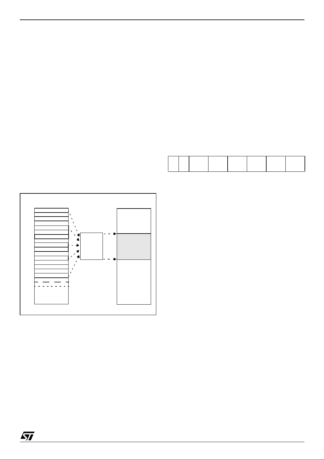
3 MEMORY MAPS, PROGRAMMING MODES AND OPTION BYTES
3.1 MEMORY AND REGISTER MAPS
3.1.1 Introd uct i on
The MCU operates in three separate memory
spaces: Program space, Data space, and Stack
space. Operation in these three memory spaces is
described in the following paragraphs.
Figure 3. Mem ory Addressing Dia gram
PROGRAM SPACE
000h
PROGRAM
MEMORY
(see Figure 4
on page 10)
0FF0h
INTERRUPT &
RESET VECTORS
0FFFh
Briefly, Program space contains user program
code in OTP and user vectors; Data space contains user data in RAM and in OTP, and Stack
space accommodat es six levels of stack for subroutine and interrupt service routine nesting.
DATA SPACE
000h
RESERVED
03Fh
040h
DATA READ-ONLY
MEMORY WINDOW
07Fh
080h
081h
082h
083h
084h
0BFh
0C0h
0FFh
X REGISTER
Y REGISTER
V REGISTER
W REGISTER
RAM
HARDWARE
CONTROL
REGISTERS
(see Table 2)
ACCUMULATOR
9/105
1
Page 10
ST6215C/ST6225C
MEMORY MAP (Cont’d)
Figure 4. Program Memory Map
ST6215C ST6225C
0000h
NOT IMPLEMENTED
07FFh
0800h
RESERVED
087Fh
0880h
USER
PROGRAM MEMORY
1824 BYTES
*
0000h
07Fh
080h
RESERVED
*
USER
PROGRAM ME M OR Y
3872 BYTES
0F9Fh
0FA0h
0FEFh
0FF0h
0FF7h
0FF8h
0FFBh
0FFCh
0FFDh
0FFEh
0FFFh
RESERVED
INTE RR U PT VECTOR S
RESERVED
NMI VECTOR
USER RESET VECTOR
*
*
(*) Reserved areas should be filled with 0FFh
0F9Fh
0FA0h
0FEFh
0FF0h
0FF7h
0FF8h
0FFBh
0FFCh
0FFDh
0FFEh
0FFFh
RESERVED
*
INTERRUPT VECTORS
RESERVED
*
NMI VECTOR
USER RESET VECTOR
10/105
1
Page 11

MEMORY MAP (Cont’d)
3.1.2 Program Space
Program Space comprises the instructions to b e
executed, the data required for immediate addressing mode instructions, the reserved factory
test area and the user v ectors. Program Space is
addressed via the 12-bit Program Counter register
(PC register). Thus, the MCU is capable of addressing 4K bytes of memory directly.
3.1.3 Readout Protection
The Program Mem ory i n O TP or E P ROM devices
can be protected against external readout of memory by setting the Readout Protection bit in the opti on byte (Section 3.3 on page 16).
In the EPROM parts, Readout Protection option
can be desactivated only by U.V. erasure that also
results in the whole EPROM context being erased.
Note: Once the Readout Protection is activated, it
is no longer possible, even for STMicroelectronics,
to gain access to the OTP contents. Returned
parts can therefore not be accepted if the Readout
Protection bit is set.
3.1.4 Data Space
Data Space accommodates all the data necessary
for processing the user program. This space comprises the RAM resource, the proc essor core an d
peripheral registers, as well as read-only data
ST6215C/ST6225C
such as constants and look-up tables in OTP/
EPROM.
3.1.4.1 Data ROM
All read-only data is physically stored in program
memory, which also accommodates the Program
Space. The program m emory consequently contains the program code to be executed, as well as
the constants and look-up tables required by t he
application.
The Data Space locations in which the different
constants and look-up tables are addressed by the
processor core may be thought of as a 64-byte
window through which it is possible to acc ess the
read-only data stored in OTP/EPROM.
3.1.4.2 Data RAM
The data space includes the user RAM area, the
accumulator (A), the indirect registers (X), (Y), the
short direct registers (V), (W), the I/O port registers, the peripheral data and control registers, the
interrupt option register and the Data ROM Window register (DRWR register).
3.1.5 Stack Space
Stack space consists of six 12-bit registers which
are used to stack subroutine and interrupt return
addresses, as well as the current program counter
contents.
11/105
1
Page 12

ST6215C/ST6225C
MEMORY MAP (Cont’d)
Table 2. Hardware Register Map
Address Block
080h
to 083h
0C0h
0C1h
0C2h
0C3h Reserved (1 Byte)
0C4h
0C5h
0C6h
0C7h Reserved (1 Byte)
0C8h CPU IOR Interrupt Option Register xxh Write-only
0C9h ROM DRWR Data ROM Window register xxh Write-only
0CAh
0CBh
0CCh
0CDh
0CEh
0CFh Reserved (1 byte)
CPU X,Y,V,W
I/O Ports
I/O Ports
I/O Ports
Register
Label
1) 2) 3)
DRA
1) 2) 3)
DRB
1) 2) 3)
DRC
DDRA
DDRB
DDRC
2)
ORA
2)
ORB
2)
ORC
2)
X,Y index registers
V,W short direct registers
Port A Data Register
Port B Data Register
Port C Data Register
Port A Direction Register
2)
Port B Direction Register
2)
Port C Direction Register
Port A Option Register
Port B Option Register
Port C Option Register
Register Name
Reserved (2 Bytes)
Reset
Status
xxh R/W
00h
00h
00h
00h
00h
00h
00h
00h
00h
Remarks
R/W
R/W
R/W
R/W
R/W
R/W
R/W
R/W
R/W
0D0h
0D1h
0D2h
0D3h
0D4h
0D5h
to 0D7h
0D8h
0D9h
to 0FEh
0FFh CPU A Accumulator xxh R/W
ADC
Timer1
Watchdog
Timer
ADR
ADCR
PSCR
TCR
TSCR
WDGR Watchdog Register 0FEh R/W
A/D Converter Data Register
A/D Converter Control Register
Timer 1 Prescaler Register
Timer 1 Counter Register
Timer 1 Status Control Register
Reserved (3 Bytes)
Reserved (38 Bytes)
xxh
40h
7Fh
0FFh
00h
Read-only
Ro/Wo
R/W
R/W
R/W
Legend:
x = undefined, R/W = Read/Write, Ro = Read-only Bit(s) in the register, Wo = Write-only Bit(s)
in the register.
Notes:
1. The contents of the I/O p ort D R registers are read able only in output configuration. In i nput c onfiguration, the values of the I/O pins are returned instead of the DR register contents.
2. The bits associated with unavailable pins must always be kept at their reset value.
3. Do not use single-bit instructions (SET, RES...) on Port Data Registers if any pin of the port is configured
in input mode (refer to Section 8 "I/O PORTS" on page 38 for more details).
12/105
1
Page 13
MEMORY MAP (Cont’d)
3.1.6 Data ROM Window Mechanism
The Data read-only memory window is located
from address 0040h to address 007Fh in Data
space. It allows direct reading of 64 consecutive
bytes located anywhere in program memory, between address 0000h and 0FFFh.
There are 64 blocks of 64 bytes in a 4K device:
– Block 0 is related to the address range 0000h to
003Fh.
– Block 1 is related to the address range 0040h to
007Fh.
and so on...
All the program memory can therefore be used to
store either instructions or read-only data. The
Data ROM window can be moved in st eps of 64
bytes along the program memory by writing the
appropriate code in the Data ROM Window Register (DRWR).
Figure 5. Data R OM Window
0000h
PROGRAM
SPACE
64-BYTE
ROM
DATA SPACE
000h
040h
DATA ROM
07Fh
WINDOW
ST6215C/ST6225C
3.1.6.1 Data ROM Window Register (DRWR)
The DRWR can be a ddressed li ke any RAM location in the Data Space.
This register is used to sele ct the 64-byt e blo ck of
program memory to be read in the Data ROM window (from address 40h to address 7Fh in Data
space). The DRWR register is not clea red on reset, therefore it must be written to before accessing the Data read-on ly memory window area for
the first time .
Address: 0C9h — Write Only
Reset Value = xxh (undefined)
70
- - DRWR5 DRWR4 DRWR3 DRWR2 DRWR1 DRWR0
Bits 7:6 = Reserved, must be cleared.
Bits 5:0 = DRWR[5:0]
Window Register Bits.
only memory Window bits that correspond to the
upper bits of the data read-only memory space.
Caution:
This register is undefined on reset, it is
write-only, therefore do not read it nor access it using Read-Modify-Write instructions (SET, RES,
INC and DEC).
Data read-only memory
These are the Da ta read-
0FFFh
0FFh
13/105
1
Page 14
ST6215C/ST6225C
MEMORY MAP (Cont’d)
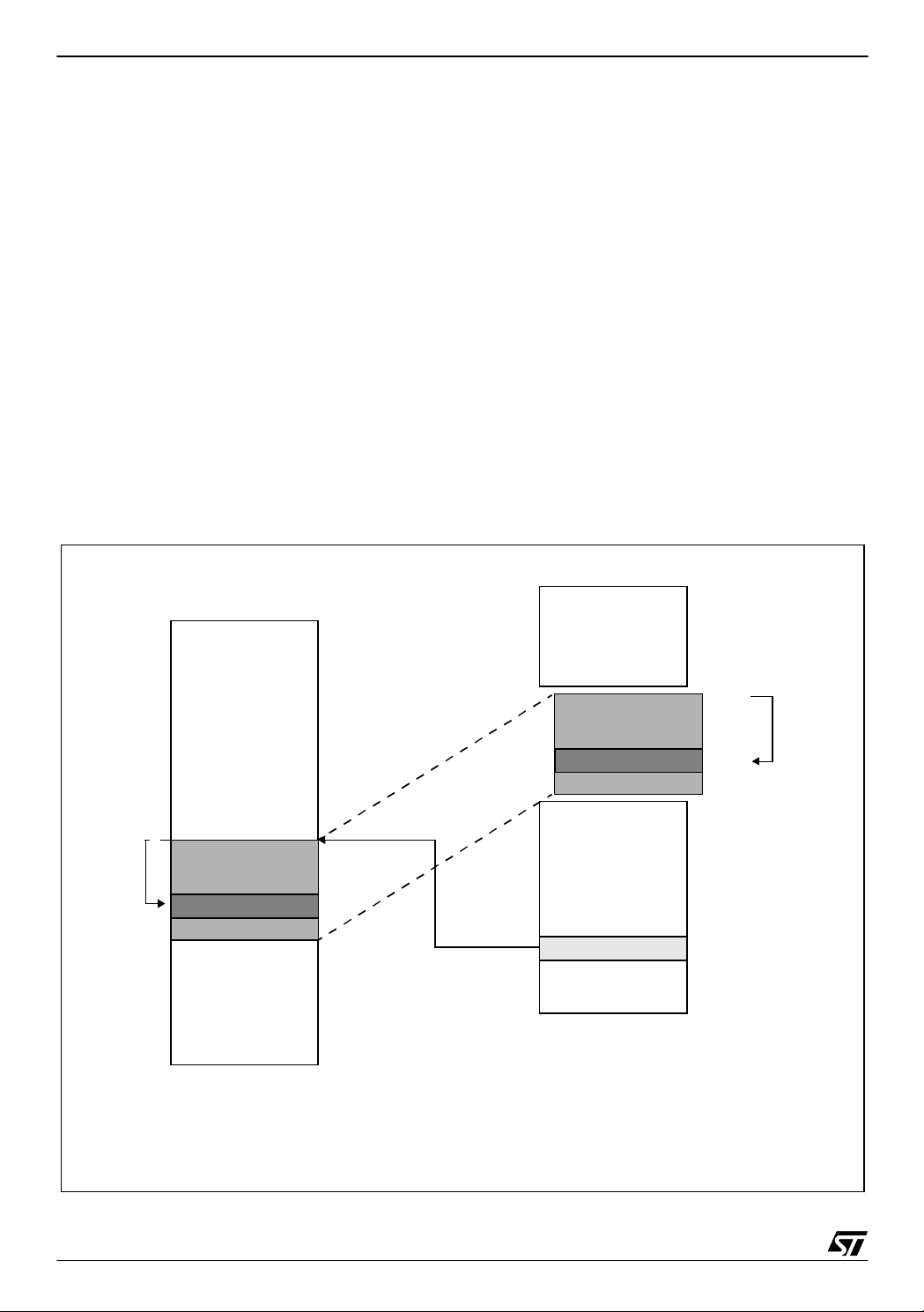
3.1.6.2 Data ROM Window memory addressing
In cases where some data (look-up tables for example) are stored in program memory, reading
these data requires the use of the Data ROM window mechanism. To do this:
1. The DRWR register ha s to be loaded with the
64-byte block number where the data are located
(in program memory). This number also gives the
start address of the block.
2. Then, the offset address of the byte in th e Data
ROM Window (corresponding to the offset in the
64-byte block in program memory) has to be loaded in a register (A, X,...).
When the above two steps are completed, the
data can be read.
To understand how to determine the DRWR and
the content of th e register, please refer to t he example shown in Figure 6. I n any c ase t he c alcul a-
Figure 6. Data read-only memory Window Memo ry Add ressi ng
tion is automatically hand led by the ST6 deve lopment tools.
Please refer to the user manual of the corres poding tool.
3.1.6.3 Recommendations
Care is required when handling the DRWR register as it is write only. For this reason, the DRWR
contents should not be chan ged while executing
an interrupt service routine, as the service routine
cannot save and then restore the register’s previous contents. If it is imp ossible to avoi d writing to
the DRWR during the interrupt service routine, an
image of the register must be saved in a RAM location, and each time the program writes to the
DRWR, it must also write to the image register.
The image register must be written first so that, if
an interrupt occurs between the two instructions,
the DRWR is not affected.
0000h
0400h
OFFSET
0421h
07FFh
PROGRAM SPACE
64 bytes
DATA
DATA SPACE
DATA
10h
000h
040h
061h
07Fh
DRWR
0FFh
OFFSET
21h
DATA address in Program memory : 421h
DRWR content : 421h / 3Fh (64) = 10H data is located in 64-bytes window number 10h
64-byte window start address : 10h x 3Fh = 400h
Register (A, X,...)content : Offset = (421h - 400h) + 40h ( Data ROM Window start address in data space) = 61h
14/105
1
Page 15

3.2 PROGRAMMING MODES
ST6215C/ST6225C
3.2.1 Program Memory
EPROM/OTP programming mode is set by a
+12.5V voltage a pplied to the T EST/V
pin. The
PP
programming flow of the ST62T15C,T25C/E25C is
described in the User Manual of the EPROM Programming Board.
Table 3. ST6215C Program Memory M ap
Device Address Description
0000h-087F h
0880h-0F9F h
0FA0h-0FEF h
0FF0h-0FF7 h
0FF8h-0FFB h
0FFCh-0FFD h
0FFEh-0FFF h
Reserved
User ROM
Reserved
Interrupt Vectors
Reserved
NMI Interrupt Vector
Reset Vector
Table 4. ST6225C Program Memory M ap
Device Address Description
0000h-007F h
0080h-0F9F h
0FA0h-0FEF h
0FF0h-0FF7 h
0FF8h-0FFB h
0FFCh-0FFD h
0FFEh-0FFF h
Reserved
User ROM
Reserved
Interrupt Vectors
Reserved
NMI Interrupt Vector
Reset Vector
Note: OTP/EPROM devices c an be programmed
with the development tools available from
STMicroelectronics (please refer to Section 13 on
page 100).
3.2.2 EPROM Erasing
The EPROM devices can be erased by exposure
to Ultra Violet light. The characteristics of the MCU
are such that erasure begins when the memory is
exposed to light with a wave lengths shorter than
approximately 4000Å. It should be noted that sunlight and some types of fluorescent lamps have
wavelengths in the range 3000-4000Å.
It is thus recommended that the window of the
MCU packages be covered by an opaque label to
prevent unintentional erasure problems when testing the application in such an environment.
The recommended erasure procedure is exposure
to short wave u ltraviolet light whi ch have a wavelength 2537Å. The integrated dose (i.e. U.V. intensity x exposure time) for erasure should be a minimum of 30W-sec/cm
dosage is approximately 30 to 40 minutes using an
ultraviolet lamp with 12000µW/cm
2
. The erasure time with this
2
power rating.
The EPROM device should be placed within
2.5cm (1inch) of the lamp tubes during erasure.
15/105
1
Page 16

ST6215C/ST6225C
3.3 OPTION BYTES
Each device is available for production in user programmable versions (OTP) as well as in factory
coded versions (ROM). O TP d evices are shippe d
to customers with a default content (00h), while
ROM factory coded parts contain the code supplied by the customer. This implies that OTP devices have to be configured by the customer using
the Option Bytes while the ROM devices are factory-configured.
The two option b ytes allow t he hardware configuration of the microcontroller to be selected.
The option bytes have no address in the memory
map and can be accessed only in programming
mode (for example using a standard ST6 programming tool).
In masked ROM devices, the option bytes are
fixed in hardware by the ROM code (see Section
12.6.2 "ROM Version" on page 98). It is therefore
impossible to read the option bytes.
The option bytes can be only programmed once. It
is not possible to change the selected options after
they have been programmed.
In order to reach the power consumption value indicated in Section 11.4, the option byte must be
programmed to its default value. Otherwise, an
over-consumption will occur.
MSB OPTION BY TE
Bits 15:10 = Reserved, must be always cleared.
0: Low Voltage Detector disabled
1: Low Voltage Detector enabled.
LSB OPTION BYTE
Bit 7 = PROTECT
Readout Protection.
This option bit enables or disables external access
to the internal program memory.
0: Program memory not read-out protected
1: Program memory read-out protected
Bit 6 = OSC
Oscillator s elec tion
.
This option bit selects the main oscillator type.
0: Quartz crystal, ceramic resonator or external
clock
1: RC network
Bits 5:4 = Reserved, must be always cleared.
Bit 3 = NMI PULL
NMI Pull-Up
on/off.
This option bit enables or disables the internal pullup on the NMI pin.
0: Pull-up disabled
1: Pull-up enabled
Bit 2 = TIM PULL
TIMER Pull-Up
on/off.
This option bit enables or disables the internal pullup on the TIMER pin.
0: Pull-up disabled
1: Pull-up enabled
Bit 9 = EXTCNTL
External STO P MO DE control.
0: EXTCNTL mode not available. STOP mode is
not available with the watchdog active.
1: EXTCNTL mode available. STOP mode is avail-
able with the watchdog active by setting NMI pin
to one.
Bit 8 = LVD
Low Voltage Detector
on/off
.
This option bit enable or disable the Low Voltage
Dete ctor (LVD ) feature.
MSB OPTION BYTE
15 8
EXT
CTL
Default
Value
16/105
Reserved
XXXXXXXXXXXXX X XX
Bit 1 = WDACT
Hardware or software watchdog.
This option bit selects the watchdog type.
0: Software (watchdog to be enabled by software)
1: Hardware (watchdog always enabled)
Bit 0 = OSGEN
Oscillator Safeguard
on/off.
This option bit enables or disables the oscillator
Safeguard (OSG) feature.
0: Oscillator Safeguard disabled
1: Oscillator Safeguard enabled
LSB OPTION BYTE
70
LVD
PRO-
OSC Res. Res.
TECT
NMI
PULL
TIM
PULLWDACT
OSG
EN
1
Page 17
4 CENTRAL PRO CESSING UNIT
ST6215C/ST6225C
4.1 INTRODUCTION
The CPU Core of ST6 devices is independent of the
I/O or Memory conf iguration. As such, it may b e
thought of as an independent central processor
communicating with on-chip I/O, Memory and Peripherals via internal address, data, and control
buses.
4.2 MAIN FEATURES
■ 40 basic instructions
■ 9 main addressing modes
■ Two 8-bit index registers
■ Two 8-bit short direct registers
■ Low power modes
■ Maskable hardware interrupts
■ 6-level hardware stack
4.3 CPU REGISTERS
The ST6 Family CPU core features six registers and
three pairs of flags available to the programmer.
These are described in the following paragraphs.
Accumulator (A). The accumulator is an 8-bit
general purpose register used in all arithmetic calculations, logical operations, and data manipula-
tions. The accumulator can be addressed i n Data
Space as a RAM lo cation at address FFh. Thus
the ST6 can manipulate the accumulator just like
any other register in Data Space.
Index Registers (X, Y). Th ese two registers are
used in Indirect addressing mode as pointers to
memory locations in Data Space. They can also
be accessed in Direct, Short Direct, or Bi t Direct
addressing modes. They are mapped in Data
Space at addresses 80h (X ) and 81h (Y) an d can
be accessed like any other memory location.
Short Direct Registers (V, W). The se two registers are used in Short Direct addressing mode.
This means that the data stored in V or W can be
accessed with a one-byte instruction (four CPU cycles). V and W can also be accessed using Di rect
and Bit Direct addressing modes. They are
mapped in Data Space at addresses 82h (V) and
83h (W) and can be accessed like any other memory location.
Note: The X and Y registers can also be used as
Short Direct registers in the same way as V and W.
Program Counter (PC). The program counter is a
12-bit register which cont ains the address of the
next instruction to be executed by the c ore. This
ROM location may be an opc ode, an operand, or
the address of an operand.
Figure 7. CPU Registers
70
ACCUMULA T OR
RESET VALUE = xxh
70
X INDEX REGISTER
RESET VALUE = xxh
70
Y INDEX REGISTER
RESET VALUE = xxh
70
RESET VALUE = xxh
70
RESET VALUE = xxh
11
RESET VALUE = RESET VECTOR @ 0FFEh-0FFFh
V SHORT INDIRECT
W SHORT INDIRECT
0
PROGRAM COUNTER
REGISTER
REGISTER
SIX LEVEL
STACK
NORMAL FLAGS
INTERRUPT FLAGS
NMI FLAGS
CN ZN
CI ZI
CNMI ZNMI
x = Undefined value
17/105
1
Page 18
ST6215C/ST6225C
CPU REGISTERS (Cont’d)
The 12-bit length allows the direct addressing of
4096 bytes in Program Space.
However, if the program space contains more than
4096 bytes, the additional memory in program
space can be addressed by using the Program
ROM Page register.
The PC value is incremented after reading the address of the current instruction. To execute relative
jumps, the PC and the offset are shifted through
the ALU, where they are added; the result is then
shifted back into the PC. The program counter can
be changed in the following ways:
– JP (Jump) instruction PC = Jump address
– CALL instruction PC = Call address
– Relative Branch InstructionPC = PC +/- offset
– Interrupt PC = Interrupt vector
– Reset PC = Reset vector
– RET & RETI instructions PC = Pop (stack)
– Normal instruction PC = PC + 1
Flags (C, Z). The ST6 CPU includes three pairs of
flags (Carry and Zero), each pair being associated
with one of the three normal modes of operation:
Normal mode, Interrupt mode and Non Maskabl e
Interrupt mode. Each pair consists of a CARRY
flag and a ZERO flag. One pair (CN, ZN) is u sed
during Normal operation, another pair is used during Interrupt mode (CI, ZI), and a third pair is used
in the Non Maskable Interrupt m ode (CNMI, ZNMI).
The ST6 CPU uses the pair of flags associated
with the current mode: as soon as an interrupt (or
a Non Maskable I nterrupt) is generated, the ST 6
CPU uses the Interrupt flags (or the NMI flag s) instead of the Normal flags. When the RETI instruction is executed, the previously used set of flags is
restored. It should be noted that ea ch flag s et can
only be addressed in its own context (Non Maskable Interrupt, Normal Interrupt or Main routine).
The flags are not cleared during context swi tching
and thus retain their status.
C : Carry flag.
This bit is set when a carry or a borrow occurs dur-
ing arithmetic operations; otherwise it is cleared.
The Carry flag is also set to the val ue of the bit
tested in a bit test instruction; it also participates in
the rotate left instruction.
0: No carry has occured
1: A carry has occured
Z : Zero flag
This flag is set if the result of the last arithmetic or
logical operation was equal to zero; otherwise it is
cleared.
0: The result of the last operation is different from
zero
1: The result of the last operation is zero
Switching between the three sets of flags is per-
formed automatically when an NMI, an interrupt or
a RETI instruction occurs. As NMI mode is automatically selected after the reset of the MCU, the
ST6 core uses the NMI flags first.
Stack. The ST6 CPU includes a true LIFO (Last In
First Out) hardware stack which eliminates the
need for a stack pointer. The stack consists of six
separate 12-bit RAM locations that do not belong
to the data space RAM area. When a subroutine
call (or interrupt request) oc curs, the contents of
each level are shifted into the next level down,
while the content of the PC is shifted into the first
level (the original contents of the sixth stack level
are lost). When a subroutine or interrupt return occurs (RET or RETI instructions), the first level register is shifted back into the PC and the value of
each level is popped back into the previous level.
Figure 8. Stack manipulation
PROGRAM
COUNTER
ON RETURN
FROM
INTERRUPT,
OR
SUBROUTINE
LEVEL 1
LEVEL 2
LEVEL 3
LEVEL 4
LEVEL 5
LEVEL 6
ON
INTERRUPT,
OR
SUBROUTINE
CALL
Since the accumulator, in common with all other
data space registers, is not stored in this stack,
management of these registers should be performed within the subroutine.
Caution: The stack will remain in its “deepest” position if more than 6 nested calls or interrupts are
executed, and consequently the last return address will be lost.
It will also remain in its highest position if the stack
is empty and a RET or RETI is executed. In this
case the nex t in s truc t io n w ill be ex e c ut e d.
18/105
1
Page 19

5 CLOCKS, SUPPLY AND RESET
5.1 CLOCK SYSTEM
ST6215C/ST6225C
The main oscillator of the MCU can be driven by
any of these cl ock sourc es:
– external clock signal
– external AT-cut parallel-resonant crystal
– external ceramic resonator
– external RC network (R
NET
).
In addition, an on-chip Low Frequency Auxiliary
Oscillator (LFAO) is available as a back-up c lock
system or to reduce power consumption.
An optional Oscillator Safeguard (OSG) filters
spikes from the oscillator lines, and switches to the
LFAO backup oscillator in t he event of m ain oscillator failure. It also automatically limits the internal
clock frequency (f
to guarantee correct operation. These functions
) as a function of VDD, in order
INT
are illustrated in Figure 10, and Figure 11.
Figure 9. Clock Circuit Block Diagram
OSCILLATOR SAFEGUA RD (OSG)
f
OSC
OSG
filtering
Table 5 illustrat es var ious poss ible os cillator c on-
figurations using an external crystal or ceramic
resonator, an external clock input, an external resistor (R
), or the lowest cost solution using only
NET
the LFAO.
For more details on c onfiguring the c lock options,
refer to the Option Bytes section of this document.
The internal MCU clock frequency (f
) is divided
INT
by 12 to drive the T imer, the Wat chdog timer and
the A/D converter, by 13 to drive the CPU core and
the SPI and by 1 or 3 to drive the ARTIMER, as
shown in Figure 9.
With an 8 M Hz o s c illat o r, the fastes t CP U cycle is
therefore 1.625µs.
A CPU cycle is the smallest unit of time needed to
execute any operation (f or instance, to increment
the Program Counter). An instruction may require
two, four, or five CPU cycles for execution.
:
13
SPI
CORE
8-BIT TIMER
MAIN
OSCILLATOR
0
1
LFAO
OSCOFF BIT
(ADCR REGISTER)
OSG ENABLE OPTION BIT (See OPTION BYTE SECTION)
Oscillator
Divider
f
INT
:
12
: 1
: 3
WATCHDOG
ADC
8-BIT ARTIMER
8-BIT ARTIMER
19/105
1
Page 20

ST6215C/ST6225C
CLOCK SYSTEM (Cont’d)
5.1.1 Main Oscillator
The oscillator configuration is specified by selecting the appropriate option in the option bytes (refer
to the Option Bytes section of this document).
When the CRYSTAL/RESONATOR option is selected, it must be used with a quartz crystal, a ceramic resonator or an external signal provided on
the OSCin pin. When the RC NETWORK option is
selected, the system clock is generated by an external resistor (the capacitor is imple men ted internally).
The main oscillator can be turned off (when the
OSG ENABLED option is selected) by setting the
OSCOFF bit of the ADC Control Register (not
available on some devices). This will automatically
start the Low Frequency Auxiliary Oscillator
(LFAO).
The main oscillator can be turned off by resetting
the OSCOFF bit of the A/D Converter Control Register or by resetting the MCU. When the main oscillator starts there is a delay made up of the oscillator start-up delay period plus the duration of the
software instruction at a clock frequency f
Caution: It should be noted that when t he RC network option is selected, the accuracy of the frequency is about 20% so it may not be suitable for
some applications (For more details, please refer
to the Electrical Characteristics Section).
LFAO
.
Table 5. Oscillator Configurations
Hardware Configuration
1)
Crystal/Resonator Option
1)
C
Crystal/Resonator Option
1)
External Clock
ST6
OSCin OSCout
NC
EXTERNAL
CLOCK
Crystal/Resonator Clock
OSCin OSCout
L1
OSCin OSCout
ST6
LOAD
CAPACITORS
RC Network
ST6
3)
2)
C
L2
NC
R
NET
RC Network Option
1)
OSG Enabled Option
Notes:
1. To select the options sho wn in column 1 of the abo ve
table, refer to the Option Byte section.
2.This schematic are given for guidance only and are subject to the schematics given by the crystal or ceramic resonator manufacturer.
3. For more details, plea se refer to the Electric al Char acteristics Section.
LFAO
ST6
OSCin OSCout
NC
20/105
1
Page 21
CLOCK SYSTEM (Cont’d)
5.1.2 Oscillator Safeguard (OSG)
The Oscillator Safeguard (OSG) feature is a
means of dramatically improving the operational
integrity of the MCU. It is available when the OSG
ENABLED option is selected in the option byte (refer to the Option Bytes section of this document).
The OSG acts as a filter whose cross-over frequency is device dependent and provides three
basic functions:
– Filt er ing s pik e s on the os c illator lines whic h
would result in driving the CPU at excessive frequencies
– Manag eme nt of the Low Frequency Auxiliary
Oscillator (LFAO), (useable as low cost internal
clock source , backup clock i n ca se of main oscillator failure or for low power consumption)
– Automatically limiting the f
clock frequency as
INT
a function of supply voltage, to ensure correct
operation even if the power supply drops.
5.1.2.1 Spike Filtering
Spikes on the oscillator lines result in an effectively
increased internal clock frequency. In the absence
of an OSG circuit, this may lead to an over frequency for a given power supply voltage. The
OSG filters out such spikes (as illustrated in Figure
10). In all cases, when the OSG is active, the max-
ST6215C/ST6225C
imum internal clock frequency, f
, which is supply voltage dependent.
f
OSG
5.1.2.2 Management of Supply Voltage
Variations
Over-frequency, at a given power supp ly level, is
seen by the OSG as spikes; it therefore filte rs out
some cycles in order that the internal clock frequency of the device is kept within the range t he
particular device can stand (depending o n V
and below f
: the maximum authorised frequen-
OSG
cy with OSG enabled.
5.1.2.3 LFAO Managemen t
When the OSG is enabled, the Low Frequency
Auxiliary Oscillator can be used (see Section
5.1.3).
Note: The OSG should be used wherever possible
as it provides maxim um security for the ap plication. It should be noted however, that it can increase power consumption and reduce the maximum operating frequency to f
Characteristics section).
Caution: Care has to be taken when using the
OSG, as the internal frequency is defined between
a minimum and a maximum value and may vary
depending on both V
cise timing measurement s, it is not recom men ded
and temperature. For pre-
DD
to use the OSG.
, is limited to
INT
(see Electrical
OSG
DD
),
Figure 10. OSG Filtering Function
f
OSC>fOSG
f
OSC
f
OSG
f
INT
Figure 11. LFA O Oscillator Funct i on
MAIN OSCILLATOR
STOPS
f
OSC
f
LFAO
f
INT
MAIN OSCILLA TOR
RESTARTS
INTERNAL CLOCK DRIVEN BY LFAO
f
OSC<fOSG
21/105
1
Page 22

ST6215C/ST6225C
CLOCK SYSTEM (Cont’d)
5.1.3 Low Frequency Auxiliary Oscillator
(LFAO)
The Low Frequency Auxiliary Oscillator has three
main purposes. Firstly, it can be used to reduce
power consumption in non timing critical routines.
Secondly, it offers a fully integrated system clock,
without any external components. Lastly, it acts as
a backup oscillator in case of m ain oscillator failure.
This oscillator is available when the OSG ENABLED option is selected in the option byte (refer to
the Option Bytes section of this document). In this
case, it automatically starts one of its periods after
the first missing edge of t he m ain os cillator, whatever the reason for the failure (main oscillator defective, no clock circuit ry prov i ded, m ain o scillat or
switched off...). See Figure 11.
User code, normal interrupts, WAIT and STOP instructions, are processed as normal, at the reduced f
cy is decreased, since the internal frequency is below 1.2 MHz .
At power on, until the main oscillator starts, the reset delay counter is driven by the LFAO. If the
main oscillator starts before the 2048 cycle delay
has elapsed, it takes over.
frequency. The A/D converter accura-
LFAO
The Low Frequency Auxiliary Oscillator is automatically switched off as soon as the main oscillator starts.
5.1.4 Register Description
ADC CONTROL REGISTER (ADCR)
Address: 0D1h — Read/Write
Reset value: 0100 0000 (40h)
70
ADCR7ADCR6ADCR5ADCR4ADCR3OSC
Bit 7:3, 1:0 = ADCR[7:3], ADCR[1:0]
Register
.
ADCR1ADCR
OFF
ADC Control
0
These bits are used to control the A/D converter (if
available on the device) otherwise they are not
used.
Bit 2 = OSCOFF
Main Oscillator Off.
0: Main oscillator enabled
1: Main oscillator disabled
Note: The OSG must be enabled using the OSGEN option in the Opt ion Byte, otherw ise t he OSCOFF setting has no effect.
22/105
1
Page 23
5.2 LOW VOLTAGE DETECTOR (LVD)
ST6215C/ST6225C
The on-chip Low Voltage De tector is enabled by
setting a bit in the option bytes (refer to the Option
Bytes section of this document).
The LVD allows the device to be used without any
external RESET circuitry. In this ca se , th e RESET
pin should be left unconnected.
If the LVD is not used, an external circuit is mandatory to ensure correct Power On R eset operation,
see figure in the Reset section. For more details,
please refer to the application note AN669.
The LVD generates a static Reset when the supply
voltage is below a reference value. This means
that it secures the power-up as well as the powerdown keeping the ST6 in reset.
The V
than the V
reference value for a voltage drop is lower
IT-
reference value for power-on in order
IT+
to avoid a parasitic reset when the MCU starts running and sinks current on the supply (hysteresis).
Figure 12. Low Voltage Detector Reset
V
DD
V
IT+
V
IT-
The LVD Reset circuitry gene rates a reset when
V
is below:
DD
when VDD is rising
– V
IT+
– V
when VDD is falling
IT-
The LVD function is illustrated in Figur e 12.
If the LVD is enabled, the MCU can be in only one
of two states:
– Over the input threshold voltage, it is running un-
der full software control
– Below the input threshold voltage, it is in static
safe reset
In these conditions, secure operation is guaranteed without the need for external reset hardware.
During a Low Voltage Detector Reset, the RESET
pin is held low, thus p ermitting the MCU to reset
other devices.
V
hyst
RESET
23/105
1
Page 24

ST6215C/ST6225C
5.3 RESET
5.3.1 Introd uct i on
The MCU can be reset in three ways:
■ A low pulse input on the RESET pin
■ Internal Watchdog reset
■ Internal Low Voltage Detector (LVD) reset
5.3.2 RESET Sequence
The basic RESET sequence consists of 3 main
phases:
■ Internal (watchdog or LVD) or external Reset
event
■ A delay of 2048 clock (f
■ RESET vector fetch
INT
) cycles
The reset delay allows the oscillator to stabilise
and ensures that recovery ha s taken place from
the Reset state.
Figure 13. RESET Sequence
V
DD
V
IT+
V
IT-
The RESET vector fetch phase duration is 2 clock
cycles.
When a reset occurs:
– The stack is cleared
– The PC is loaded with the address of the Reset
vector. It is located in program ROM starting at
address 0FFEh.
A jump to the beginning of the us er program m ust
be coded at this address.
– The interrupt flag is automatically set, so that the
CPU is in Non Maskable Interrupt mode. This
prevents the initialization routine from being interrupted. The initialization routine should therefore be terminated by a RETI instruction, in order
to go back to normal mode.
WATCHDOG
RESET
LVD
RESET
RESET PIN
INTERNAL
RESET
RUN
RESET
WATCHDOG UNDERFLOW
RUN RUN RUN
RESET RESET
2048 CLOCK CYCLE (f
INT
) DELAY
24/105
1
Page 25
RESET (Cont’d)
5.3.3 RESET
The RESET
Pin
pin may be co nnecte d to a device on
the application board in order to reset the MCU if
required. The RESET
pin may be pulled low in
RUN, WAIT or STOP mode. This input can be
used to reset the internal state of the MCU and ensure it starts-up correctly. The pin, which i s connected to an internal pull-up, is active low and features a Schmitt trigger input. A delay (2048 clock
cycles) added to the external signal ensures that
even short pulses on the RESET
as valid, provided V
has completed its rising
DD
pin are accepted
phase and that the oscillator is running correctly
(normal RUN or WAIT modes). The MCU is kept in
the Reset state as long a s the RESET
pin is held
low.
Figure 14. Reset Block Diagram
ST6215C/ST6225C
If the RESET
RUN or WAIT modes, processing of the user program is stopped (RUN mode only), the I/O ports
are configured as inputs with pull-up resistors and
the main oscillator is restarted. When the level on
the RESET
quence is executed at the end of the internal delay
period.
If the RESET
STOP mode, the oscillator starts up and all the I/O
ports are configured as inputs with pull-up resistors. When the RESET
the initialization sequence is executed at th e end
of the internal delay period.
A simple external RESET circuitry is shown in Fig-
ure 15. For more details, please refer to the appli-
cation note AN669.
pin is grounded while the MCU is in
pin then goes high, the initialization se-
pin is grounded while the MCU is in
pin level then go es high,
RESET
1) Resistive ESD protection.
R
ESD
INTERNAL
f
V
DD
R
PU
1)
INT
COUNTER
clock cycles
2048
WATCHDOG RESET
LVD RESET
RESET
25/105
1
Page 26
ST6215C/ST6225C
RESET (Cont’d)
5.3.4 Watchdog Reset
The MCU provides a Wat chdog timer function in
order to be able to recover from software hangups. If the Watchdog register is not refreshed before an end-of-count condition is reached, a
Watchdog reset is generated.
After a Watchdo g reset, the MCU resta rts in the
same way as if a Reset was generated by the RESET pin.
Note: When a watchdog reset occurs, the RESET
pin is tied low for very short time period, to flag the
reset phase. This time is n ot long enough to reset
external circuits.
For more details refer to the Watchdog Timer
chapter.
5.3.5 LVD Reset
Two different RESET sequences caused by the internal LVD circuitry can be distinguished:
■ Power-On RESET
■ Voltage Drop RESET
During an LVD reset, the RESET
when V
DD
<V
(rising edge) or VDD<V
IT+
edge).
For more details, refer to the LVD chapter.
Caution: Do not externally connect directly the
RESET
pin to VDD, this may cause damage to the
component in case of internal RESET (Watchdog
or LVD).
Figure 15. Simple External Reset Circuitry
pin is pulled low
(falling
IT-
Figure 16. Reset Processing
RESET
CLOCK CYC LE
INTERNAL
RESET
NMI MASK SET
INT LATCH CLEARED
(IF PRESENT)
SELECT
NMI MODE FLA G S
PUT FFEh
ON ADDRESS BUS
YES
FROM RESET LOCATIONS
IS RESET STILL
PRESENT?
NO
LOAD PC
FFEh/FFFh
2048
DELAY
V
DD
Typical: R = 10K
C = 10nF
26/105
1
V
DD
R
RESET
C
ST62xx
R > 4.7 K
FETCH INSTRUCTION
Page 27

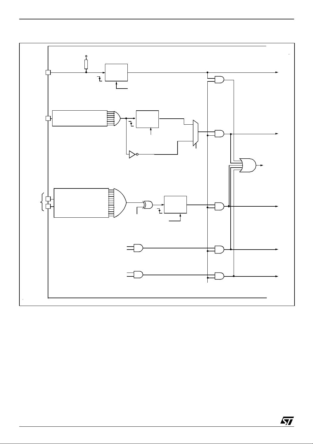
6 INTERRUPTS
ST6215C/ST6225C
The ST6 core may be interrupted by four maskable interrupt sources, in addition to a Non Maskable Interrupt (NMI) source. The interrupt processing flowchart is shown in Figure 18.
Maskable interrupts must be enabled by setting
the GEN bit in the IOR register. However, even if
they are disabled (GEN bit = 0 ), interrupt events
are latched and may be processed as soon as the
GEN bit is set.
Each source is associated with a specific Interrupt
Vector, located in Program space (see Interrupt
Mapping table). In the vector location, the user
must write a Jump instruction to the associated interrupt service routine.
When an interrupt source generates an i nterrupt
request, the PC register is loaded with the address
of the interrupt vector, which then causes a Jum p
to the relevant interrupt service routine, thus servicing the int e r ru pt.
Interrupts are triggered by events either on external pins, or from the on-chip periphe rals. Several
events can be ORed on the same interrupt vector.
On-chip peripherals have flag registers to determine which event triggered the interrupt.
27/105
1
Page 28
ST6215C/ST6225C
Figure 17. Inte rru pt s B l ock D i agra m
V
DD
PA0..PA7
PB0..PB7
PC4..PC7
NMI
I/O PORT REGISTER
“INPUT WITH INTER RUP T”
CONFIGURATION
I/O PORT REGISTER
“INPUT WITH INTER RUP T”
CONFIGURATION
LATCH
CLEARED BY H/W
AT START OF VECTOR #0 ROUTINE
CLEARED BY H/W
AT START OF
VECTOR # 1 ROUTINE
ESB BIT
(IOR REGISTER)
LATCH
(IOR REGISTER)
LATCH
CLEARED
BY H/W AT START OF
VECTOR #2 ROUTINE
VECTOR #0
0
VECTOR #1
1
LES BIT
EXIT FROM
STOP/WAIT
VECTOR #2
TIMER
(TSCR REGISTER)
A/D CONVERTER
(ADCR REG I ST E R )
TMZ BIT
ETI BIT
EAI BIT
EOC BIT
VECTOR #3
VECTOR #4
GEN BIT
(IOR REGISTER)
28/105
1
Page 29

ST6215C/ST6225C
6.1 INTERRUPT RULES AND PRIORITY MANAGEMENT
■ A Reset can interrupt the NMI and peripheral
interrupt routines
■ The Non Maskable Interrupt request has the
highest priority and can interrupt any peripheral
interrupt routine at any time but cannot interrupt
another NMI interrupt.
■ No peripheral interrupt can in terrupt another. If
more than one interrupt request is pending,
these are processed by the processor core
according to their priority level: vector #1 has the
highest priority while vector #4 the lowest. The
priority of each interrupt source is fixed by
hardware (see Interrupt Mapping table).
6.2 INTERRUPTS AND LOW POWER MODES
All interrupts cause the processor to exit from
WAIT mode. Only the external and som e specific
interrupts from the on-chip peripherals cause the
processor to exit from STOP mode (refer to the
“Exit from STOP“ column in the Interrupt Mapping
Table).
6.3 NON MASKABLE INTERRUPT
This interrupt is t riggered when a fallin g edge occurs on the NMI pin regardless of the state of the
GEN bit in the IOR register. An interrupt request
on NMI vector #0 is latched by a flip flop which is
automatically reset by the core at the beginning of
the NMI service routine.
6.4 PERIPHERAL INTERRUPTS
Different peripheral interrupt flags in the peripheral
control registers are able to cause an interrupt
when they are active if both:
– The GEN bit of the IOR register is set
– The corresponding enable bit is set in the periph-
eral control register.
Peripheral interrupts are linked to vectors #3 and
#4. Interrupt requests are flagged by a bit in their
corresponding control register. This means that a
request cannot be lost, because the flag bit m ust
be cleared by user software.
29/105
1
Page 30

ST6215C/ST6225C
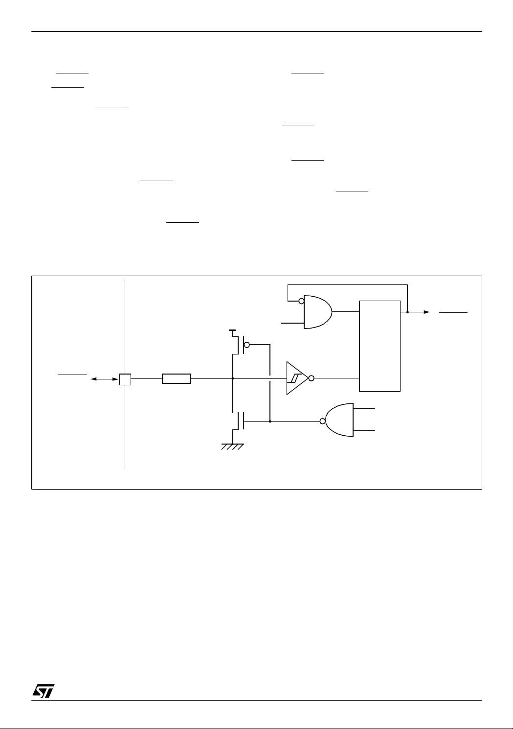
6.5 EXTERNAL INTERRUPTS (I/O Ports)
External interrupt vectors can be loaded into the
PC register if the corresponding external interrupt
occurred and if the GEN bit is set. These interrupts
allow the processor to exit from STOP mode.
The external interrupt polarity is selected t hrough
the IOR register.
External interrupts are linked to vectors #1 and #
2.
Interrupt requests on vector #1 can be configu red
either as edge or le vel-s ensitive us in g t he LES bit
in the IOR Register.
Interrupt requests from vector #2 are always edge
sensitive. The edge polarity can be configured using the ESB bit in the IOR Register.
In edge-sensitive mode, a latch is set when a edge
occurs on the interrupt source li ne and is cleared
when the associated interrupt routine is started.
So, an interrupt request can be stored until completion of the currently executing interrupt routine,
before being processed. If several interrupt requests occurs before comp let ion o f the cu rrent interrupt routine, only the first request is stored.
Storing of interrupt requests is not possible i n level
sensitive mode. To be taken into account, the lo w
level must be present on the interrupt pin when the
MCU samples the line after instruction execution.
6.5.1 Notes on using External Interrupts
ESB bit Spuri ous Interrupt on Ve c tor # 2
If a pin associated with interrupt vector #2 is configured as interrupt with pull-up, whenever vector
#2 is configured to be rising edge sensitive (by setting th e ESB b it in the I OR register ), a n interrupt i s
latched although a rising edge may not have occured on the associated pin.
This is due to the vector #2 circuitry.The workaround is to discard this first interrupt request in the
routine (using a flag for example).
Masking of One Interrupt by Another on Vector
#2.
When two or more port pins (associated with interrupt vector #2) are configured together as input
with int errupt (falling edge sensitive ), as long as
one pin is stuck at '0', the other pin can never generate an interrupt even if an act ive edge occurs at
this pin. The same thin g occurs when one pin is
stuck at '1' and interrupt vector #2 is configured as
rising edge sensitive.
To avoid this the f irst pin must input a signal that
goes back up to '1' right after the falling edge. Otherwise, in the interrupt rou tine for the first pin, deactivate the “input with interrupt” mode using the
port control registers (DDR, OR, DR). An active
edge on another pin can then be latched.
I/O port Configuration Spurious Interrupt on
Vector #2
If a pin associated with interrupt vector #2 is in ‘input with pull-up’ st ate, a ‘0’ level is present on t he
pin and the ESB bit = 0, when the I/O pin is configured as interrupt with pull-up by writing to the
DDRx, ORx and DRx register bits, an interrupt is
latched although a falling edge may not have occurred on the associated pin.
In the opposite case, if the pin is in interrupt with
pull-up state , a 0 level is present on the pin and
the ESB bit =1, when the I/O po rt is con figured as
input with pull-up by writing to the DDRx, ORx and
DRx bits, an interrupt is latched although a rising
edge may not have occurred on the associated
pin.
30/105
1
Page 31

6.6 INTERRUPT HANDLING PROCEDURE
ST6215C/ST6225C
The interrupt procedure is very similar to a call procedure, in fact the user ca n consider the interrupt
as an asynchronous call procedure. As this is an
asynchronous event, the user cannot know the
context and the time at which it occurred. As a result, the user should save all Data space registers
which may be used within the interrupt routines.
The following list summarizes the interrupt procedure:
When an interrupt request occurs, the following
actions are performed by the MCU automatically:
– The core switches from the normal flags to the
interrupt flags (or the NMI flags).
– The PC contents are stored in the top level of the
stack.
– The normal interrupt lines are inhibited (NMI still
active).
– The internal latch (if any) is cleared.
– The associated interrupt vector is loaded in the PC.
When an interrupt request occurs, the following
actions must be performed by the user software:
– User selected registers have to be saved within
the interrupt service routine (normally on a soft-
ware stack).
– The source of the interrupt must be determined
by polling the interrupt flags (if more than one
source is associated with the same vector).
– The RETI (RETurn from Interrupt) instruction
must end the interrupt service routine.
After the RETI instruction is executed, the MCU re-
turns to the main routine.
Caution: When a maskable interrupt occurs while
the ST6 core is in NORMAL mode and during the
execution of an “ldi IOR, 00h” instruction (disabling
all maskable interrupts): if the interrupt request occurs during the first 3 cycles of the “ldi” instruction
(which is a 4-cycle instruction) the core will switch
to int errupt mo de BUT the flags CN and Z N will
NOT switch to the interrupt pair CI and ZI.
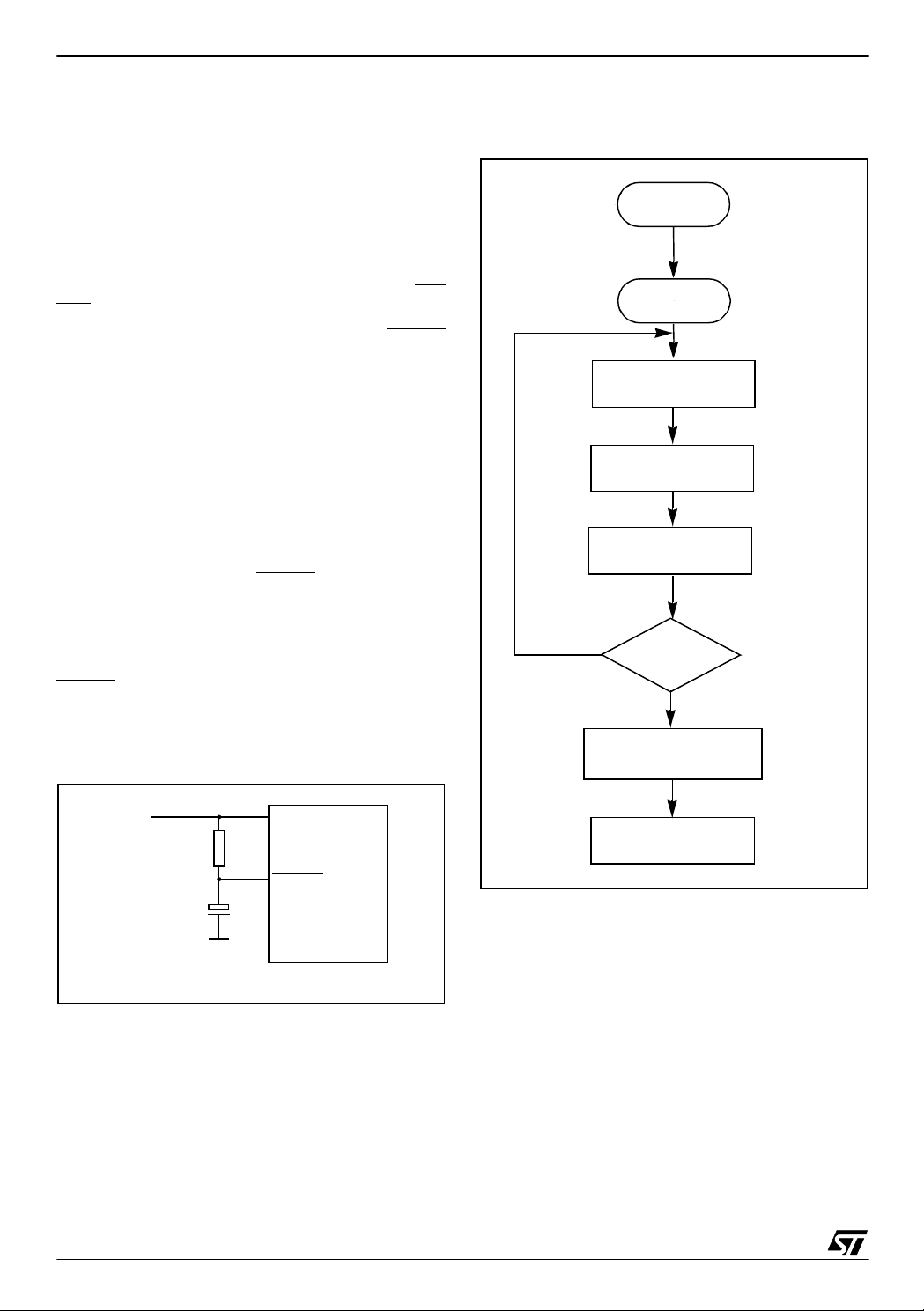
6.6.1 Interrupt Response Time
This is defined as the time between the mom ent
when the Program Counter is loaded wi th the interrupt vector and when the program has jump to
the interrupt subroutine and is ready to execute
the code. It depends on when t he in terrupt occurs
while the core is processing an instruction.
Figure 18. Interrupt Processing Flow Chart
INSTRUCTION
FETCH
INSTRUCTION
EXECUTE
INSTRUCTION
WAS
THE INSTRUCTION
YES
NORMAL MODE?
MASKABLE INTERRUPTS
THE STAC KED PC
NO
AN INTERRUPT REQUEST
AND INTERRUPT MASK?
*)
If a latch is present on the interrupt source line
?
A RETI
YES
IS THE CORE
ALREADY IN
NO
ENABLE
SELECT
NORMAL FLAGS
“POP”
IS THE R E AN
YES
NO
LOAD PC FROM
INTERRUPT VECTOR
CLEAR
INTERNAL LATCH
DISABLE
MASKABLE INTERRUPT
PUSH T H E
PC INTO T H E STACK
SELECT
INTERRUPT FLAGS
*)
Table 6. Interrupt Response Time
Minimum 6 CPU cycles
Maximum 11 CPU cycles
One CPU cycle is 13 exte rn al clock cycles thu s 1 1
CPU cycles = 11 x (13 /8M) = 17.875 µs with an 8
MHz external quartz.
31/105
1
Page 32

ST6215C/ST6225C
6.7 REGISTER DESCRIPTION INTERRUPT OPTION REGISTER (IOR)
Address: 0C8h — Write Only
1: Low level sensitive mode is selected for inter-
rupt vector #1
Reset status: 00h
70
- LES ESB GEN - - - -
Bit 5 = ESB
0: Falling edge mode on interrupt vector #2
1: Rising edge mode on interrupt vector #2
Bit 4 = GEN
Caution: This register is write-only and cannot be
accessed by single-bit operations (SET, RES,
DEC,...).
0: Disable all maskable interrupts
1: Enable all maskable int e rru p ts
Note: When the GEN bit is cleared, the NMI inter-
Edge Selection bit
Global Enable Interrupt
rupt is active but cannot be used to exit from STOP
Bit 7 =Reserved, must be cleared.
Bit 6 = LES
Level/Edge Selection bit
.
or WAIT modes.
Bits 3:0 = Reserved, must be cleared.
0: Falling edge sensitive mode is s elected for inter-
rupt vector #1
Table 7. Interrupt Mapping
Vector
number
Vector #0 NMI Non Maskable Interrupt N/A N/A yes FFCh-FFDh
Vector #1 Port A Ext. Interrupt Port A N/A N/A yes FF6h-FF7h
Vector #2 Port B, C Ext. Interrupt Port B, C N/A N/A yes FF4h-FF5h
Vector #3 TIMER Timer underflow TSCR TMZ yes FF2h-FF3h
Vector #4 ADC End Of Conversion ADCR EOC no FF0h-FF1h
Source
Block
RESET Reset N/A N/A yes FFEh-FFFh
Description
NOT USED
Register
Label
Flag
Exit
from
STOP
Vector
Address
FFAh-FFBh
FF8h-FF9h
.
.
Priority
Order
Highest
Priority
Lowest
Priority
32/105
1
Page 33

7 POWER SAVIN G MO DES
7.1 INTRODUCTION
ST6215C/ST6225C
To give a large measure of flexibility to the application in terms of power consumption, two main power saving modes are implemented in the ST6 (see
Figure 19).
In addition, the Low Frequency Auxiliary Oscillator
(LFAO) can be used inste ad of the main oscillator
to reduce power consumption in RUN and WAIT
modes.
After a RESET the normal operating mode is selected by default (RUN mode). This mode drives
the device (CPU and embedded peripherals) by
means of a master clock which is based on the
main oscillator frequency.
From Run mode, the different power saving
modes may be selected by calling the specific ST6
software instruction or for the LFAO by setting the
relevant register bit. For more information on the
LFAO, please refer to the Clock chapter.
Figure 19. Power Saving Mode Tran sitions
High
RUN
LFAO
WAIT
STOP
Low
POWER CONSUMPTION
33/105
1
Page 34

ST6215C/ST6225C
7.2 WAIT MODE
The MCU goes into WAIT mode as soon as the
WAIT instruction is executed. This has the following effects:
– Program execution is stopped, the microcontrol-
ler software can be considered as being in a “fro-
zen” state.
– RAM contents and peripheral registers are pre-
served as long as the power supply voltage is
higher than the RAM retention voltage.
– The oscillator is kept running to provide a clock
to the peripherals; they are still active.
WAIT mode can be used when the use r wants to
reduce the MCU power consumption during idle
periods, wh ile n ot lo s ing trac k o f time or the ability
to monitor external events. WAIT mode places the
MCU in a low power consumption mode by stopping the CPU. The active oscillator (main oscillator
or LFAO) is kept running in order to provide a clock
signal to the peripherals.
If the power consumption has to be further reduced, the Low Frequency Auxiliary Oscillator
(LFAO) can be used in place of the main oscillator,
if its operating frequency is lower. If requ ired, the
LFAO must be sw itched on befo re entering WA IT
mode.
Exit from Wait mode
The MCU remains in WAIT mode until one of th e
following events occurs:
– RESET (Watchdog, LVD or RESET
pin)
– A peripheral interrupt (timer, ADC,...),
– An external interrupt (I/O port, NMI)
The Program Counter then branches to the starting address of the interrupt or RESET service routine. R e fer to Figure 20.
See also Section 7.4.1 .
Figure 20. WAIT Mode Flowchart
OSCILLATOR
WAIT INSTRUCTION
N
INTERRUPT
Y
Clock to PERIPHERALSOnYes
Clock to CPU
N
RESET
Y
OSCILLATOR
Clock to PERIPHERALS
Clock to CPU
CLOCK CYCLE
DELAY
OSCILLATOR
Clock to PERIPHERALS
Clock to CPU Yes
FETCH RESET VECTOR
OR SERVICE INTERRUPT
No
Restart
Yes
Yes
2048
On
Yes
34/105
1
Page 35

7.3 STOP MODE
ST6215C/ST6225C
STOP mode is the lowest power consumption
mode of the MCU ( s ee Figure 22).
The MCU goes into STOP mode as soon as the
STOP instruction is executed. This has the following effects:
– Program execution is stopped, the microcontrol-
ler can be considered as being “frozen”.
– The contents of RAM and the peripheral regis-
ters are kept safely as long as the power supply
voltage is higher than the RAM retention voltage.
– The oscillator is stopped, so peripherals cannot
work except the those that can be driven by an
extern al clock.
Exit fr o m STOP Mo de
The MCU remains in STOP mode until one of the
following events occurs:
– RESET (Watchdog, LVD or RESET
pin)
– A peripheral interrupt (assuming this peripheral
can be driven by an external clock)
– An external interrupt (I/O port, NMI)
In all cases a delay of 2048 clock cycles (f
INT
) is
generated to make sure the oscillator has starte d
properly.
The Program Counter then points to the starting
address of the interrupt or RESET service routine
(see Figure 21).
STOP Mode and Watchdog
When the Watchdog is ac tive (hardware or software activation), the STOP instruction is disabled
and a WAIT instruction will be executed in its place
unless the EXCTNL option bit is set to 1 in the option bytes and a a high level is present on the NMI
pin. In this case, the STOP instruction will be executed and the Watchdog will be frozen.
Figure 21. STOP Mode Tim ing Over vie w
2048
STOPRUN RUN
STOP
INSTRUCTIO N
RESET
OR
INTERRUP T
CYCLECLOCK
DELAY
FETCH
VECTOR
35/105
1
Page 36
ST6215C/ST6225C
STOP MODE (Cont’d)
Figure 22. ST OP Mode Flowchart
STOP INSTRUCTION
EXCTNL
1)
VALUE
0
0
OSCILLATOR
Clock to PERIPHERALSOnYes
Clock to CPU
N
RESET
No
Y
1
LEVEL
ON
NMI PIN
N
INTERRUPT
1
Y
ENABLE
OSCILLATOR
Clock to PERIPHERALS
Clock to CPU
3)
OSCILLATOR
Clock to PERIPHERALS
Clock to CPU
WATCHDOG
N
RESET
DISABLE
Y
Off
2)
No
No
Restart
Yes
Yes
N
INTERRUPT
Y
CLOCK CYCLE
OSCILLATOR
Clock to PERIPHERALSOnYes
Clock to CPU
FETCH RESET VECTOR
OR SERVICE INT ERRUPT
2048
DELAY
Yes
Notes:
1. EXCTNL is an option bit. See option byte section for more details.
2. Peripheral clocked with an external clock source can still be active.
3. Only some specific interrupts can exit the MCU from STOP mode (such as external interrupt). Refer to
the Interrupt Mapping table for more details.
36/105
1
Page 37

7.4 NOTES RELATED TO WAIT AND STOP MODES
ST6215C/ST6225C
7.4.1 Exit from Wa i t a nd S top Modes
7.4.1.1 NMI Interrupt
It should be noted that when the GEN bit in the
IOR register is low (interrupts disabled), the NMI
interrupt is active but cannot cause a wake up from
STOP/WAIT modes.
7.4.1.2 Restart Sequence
When the MCU exits from WAIT or STOP mode, it
should be noted that the restart sequence depends on the original state of the MCU (normal, interrupt or non-maskable interrupt mode) prior to
entering WAIT or STOP mode, as well as on th e
interrupt type.
Normal Mode. If the MCU was in the main routine
when the WAIT or STO P instruction was executed, exit from Stop or Wait mode will occur as soon
as an interrupt occurs; the related interrupt routine
is executed and, on completion, the instruction
which follows the STOP or WAIT instruction is
then executed, providing no other interrupts are
pending.
Non Maskable Interrupt Mode. If the STOP or
WAIT instruction has been executed during execution of the non-maskable interrupt routine, the
MCU exits from Stop or Wait mode as soon a s a n
interrupt occurs: the instruction which follows the
STOP or WAIT instruction is executed, and the
MCU remains in non-maskable interrupt mode,
even if another interrupt has been generated.
Normal Inte rrupt Mod e. If the MCU was in interrupt mode before the STOP or WAIT instruction
was executed, it exits from STOP o r WAIT mode
as soon as an interrupt occurs. Nevertheless, t wo
cases must be considered:
– If the interrupt is a normal one, the interrupt rou-
tine in which the WAIT or STOP mode was entered will b e c o mpleted, sta rti ng with the
execution of the instruction which follows the
STOP or the WAIT instruction, and the MCU is
still in interrupt mode. At the end of this routine
pending interrupts will be serviced according to
their priority.
– In the event of a non-maskable interrupt, the
non-maskable interrupt service routine is processed first, then the routine in which the WAIT or
STOP mode was entered will be completed by
executing the instruction following the STOP or
WAIT instruction. The MCU remains in normal interrupt mode.
7.4.2 Recommended MCU Configuration
For lowest power consumption during RUN or
WAIT modes, the user software must configure
the MCU as follows:
– Configure unused I/O s as output push-pull low
mode
– Place all peripherals in their power down modes
before entering STOP mode
– Se lect the Lo w Frequency Auxiliary Oscillator
(provided this runs at a lower frequency than the
main osc illator).
The WAIT and STOP instructions are not executed if an enabled interrupt request is pending.
37/105
1
Page 38

ST6215C/ST6225C
8 I/O PORTS
8.1 INTRODUCTION
Each I/O port contains up to 8 p ins. Each pin can
be programmed independently as digital input
(with or without pull-up and interr upt generation),
digital output (open drain, push-pull) or analog input (when available).
The I/O pins can be used in eithe r standard or alternate function mode.
Standard I/O mode is used for:
– Transfer of data through digital inputs and out-
puts (on specific pins):
– External interrupt generation
Alternate function mode is used for:
– Alternate signal input/output for the on-chip
peripherals
The generic I/O block diagram is shown in Figure
23.
8.2 FUNCTIONAL DESCRIPTION
Each port is associated wi th 3 reg isters located i n
Data space:
– Data Register (DR)
– Data Direction Register (DDR)
– Option Register (OR)
Each I/O pin may be programmed using the corre-
sponding register bits in the DDR, DR and OR registers: bit x corresponding to pin x of the port. Table
8 illustrates the various port configurations which
can be selected by user software.
During MCU initialization, all I/O registers are
cleared and the input mode with pull-up and no interrupt generation is selected for all the pins, thus
avoiding pin conflicts.
8.2.1 Digital Input Modes
The input configuration is sele cted by clearing the
corresponding DDR register bit.
In this case, reading the DR register returns the
digital value applied to the external I/O pin.
Different input modes can be selected by software
through the DR and OR registers, see Table 8.
External Interrupt Function
All input lines can be individually connected by
software to the interrupt system by programming
the OR and DR registers accordingly. The interrupt trigger modes (fall ing edge, rising edge and
low level) can be configured by software for each
port as described in the Interrupt section.
8.2.2 Analog Inputs
Some pins can be configured as analog input s by
programming the OR and DR registers accordingly, see Table 8 . T hese analog inputs are conn ec ted to the on-chip 8-bit Analog to Digital Converter.
Caution: ONLY ONE
pin should be program med
as an analog input at any time, since by select ing
more than one input simultaneously their pins will
be effectively shorted.
8.2.3 Output Modes
The output configuration is selecte d by setting the
corresponding DDR register bit. In this case, writing to the DR register applies this digital value to
the I/O pin through the latch. Then, reading the DR
register returns the previously stored value.
Two different output modes can be selected by
software through the OR register: push-pull and
open-drain.
DR register value and output pin status:
DR Push-pull Open-drain
0V
1VDDFloating
SS
V
SS
Note: The open drain setting is not a true open
drain. This means it has the same structure as the
push-pull setting but the P-buffer is deactivated.
To avoid damaging the device, please respect the
absolute maximum rating described in the
V
OUT
Electrical Characteristics section.
8.2.4 Alternate Functions
When an on-chip peripheral is configured to use a
pin, the alternate function (timer input/output.. .) is
not systematically selected but has to be configured through the DDR, OR and DR registers. Refer to the chapter describing the peripheral for
more details.
38/105
1
Page 39

I/O PO R T S (Cont’d)
Figure 23. I/O Por t Bl ock D i agram
ST6215C/ST6225C
ST6
INTERNAL
BUS
TO INTERRUPT
RESET
DATA
DIRECTION
REGISTER
DATA
REGISTER
OPTION
REGISTER
PULL-UP
P-BUFFER
CMOS
SCHMITT
TRIGGER
V
DD
N-BUFFER
V
DD
V
CLAMPING
DIODES
DD
Pxx I/O Pin
TO ADC
Table 8. I/O Port Configurations
DDR OR DR Mode Option
0 0 0 Input With pull-up, no interrupt
0 0 1 Input No pull-up, no interrupt
0 1 0 Input With pull-up and with interrupt
0 1 1 Input Analog input (when available)
1 0 x Output Open-drain output (20mA sink when available)
1 1 x Output Push-pull output (20mA sink when available)
Note: x = Don’t care
39/105
1
Page 40

ST6215C/ST6225C
I/O PO R T S (Cont’d)
8.2.5 Instructions NOT to be used to access
Port Data registers (SET, RES, INC and DEC)
DO NOT USE READ-MODIFY-WRITE INSTRUCTIONS (SET, RES, INC and DEC) ON PORT
DATA REGI STERS IF ANY P IN OF TH E PORT IS
CONFIGURED IN INPUT MODE.
These instructions make an implicit read and write
back of the entire register. In port input mode,
however, the data register reads from the input
pins directly, and not from the data register latches. Since data register information in input mode is
used to set the characteristics of the input pin (interrupt, pull-up, analog input), these may be uni ntentionally reprogrammed depending on the state
of the input pins.
As a general rule, it is better to only use single bit
instructions on data registers when the whole (8bit) port is in output mode. In the case of inputs or
of mixed inputs and outputs, it is advisable to keep
a copy of the data regist er in RAM. Single bit instructions may then be used on the RAM copy, after which the whole copy register can be written to
the port data register:
SET bit, datacopy
LD a, datacopy
LD DRA, a
2. Handling Unused Port Bits
On ports that have less than 8 external pins connected:
– Leave the unbonded pin s in reset state and do
not change their configuration.
– Do not use instructions that act on a whole port
register (INC, DEC, or read operations). Unavailable bits must be masked by software (AND instruction). Thus, when a read operation
performed on an incomplete port is followed by a
comparison, use a mask.
3. High Impedance Input
On any CMOS de vice, it is not recommended to
connect high impedance on input pins. The choice
of these impedance has to be done with respect to
the maximum leakage current de fined in the datasheet. The risk is to be close o r out o f specification on the input levels applied to the device.
8.3 LOW POWER MODES
The WAIT and STOP instructions allow the
ST62xx to be used in situations where low power
consumption is needed. The lowest power consumption is achieved by configuring I/Os in output
push-pull low mode.
8.2.6 Recommendations
1. Safe I/O State Switching Sequence
WAIT
Switching the I/O ports from one state to another
should be done in a se quence which ensures that
no unwanted side effects can occur. The recom-
STOP
mended safe transitions are illustrated in Figure 24
The Interrupt Pull-up to Input Analog transition
(and vice-vesra) is potentially risky and should be
avoided when changing the I/O operating mode.
8.4 INTERRUPTS
The external interrupt event generates an interrupt
if the corresponding configuration is selected with
DDR, DR and OR registers (see Table 8) and the
GEN-bit in the IOR register is set.
Figure 24. Diagram showing Safe I/O State Transitions
Interrupt
pull-up
010*
Input
pull-up (Reset
000
state)
Output
Open Drain
Output
Push-pull
100
110
Note *. xxx = DDR, OR, DR Bits respectively
Mode Description
No effect on I/O ports. External interrupts
cause the device to exit from WAIT mode.
No effect on I/O ports. External interrupts
cause the device to exit from STOP mode.
011
001
101
111
Input
Analog
Input
Output
Open Drain
Output
Push-pul l
40/105
1
Page 41

I/O PO R T S (Cont’d)
Table 9. I/O Port Option Selections
ST6215C/ST6225C
MODE
Input
DDRx0ORx0DRx
Reset state
Input
with pull up
DDRx0ORx0DRx
Digital Input
Input
with pull up
with interrupt
DDRx0ORx1DRx
1
0
0
AVAILABLE
ON
PA0-PA7
PB0-PB7
PC4-PC7
PA0-PA7
PB0-PB7
PC4-PC7
PA0-PA7
PB0-PB7
PC4-PC7
(1)
V
DD
V
DD
V
DD
SCHEMATIC
V
DD
V
DD
V
DD
Data in
Interrupt
Data in
Interrupt
Data in
Interrupt
V
Analog Input
DDRx0ORx1DRx
Analog Input
Open drain output (5mA)
Open drain output (20 mA)
DDRx1ORx0DRx
Push-pull output (5mA)
Digital output
Push-pull output (20 mA)
DDRx1ORx1DRx
PA4-PA7
PB0-PB7
PC4-PC7
1
PA4-PA7
PB0-PB7
PC4-PC7
PA0-PA3
0/1
PA4-PA7
PB0-PB7
PC4-PC7
PA0-PA3
0/1
DD
V
DD
V
DD
Note 1. Provided the correct configuration has been selected (see Table 8).
ADC
P-buffer disconnected
Data out
Data out
41/105
1
Page 42

ST6215C/ST6225C
I/O PO R T S (Cont’d)
8.5 REGISTER DESCRIPTION DATA REGISTER (DR)
Port x Data Register
DRx with x = A, B or C.
Addresses 0C0h, 0C1h and 0C2h- Read/Write
Bits 7:0 = DDR[7:0]
Data direction register bits.
The DDR register gives the input /output direction
configuration of the pins. Each bit is set and
cleared by software.
0: Input mode
1: Output mode
Reset Value: 0000 0000 (00h)
OPTION REGISTER (OR)
70
Port x Option Register
ORx with x = A, B or C.
DR7 DR6 DR5 DR4 DR3 DR2 DR1 DR0
Bits 7:0 = DR[7:0]
Data register bits.
Addresses: 0CCh, 0CDh and 0CEh - Read/ Write
Reset Value: 0000 0000 (00h)
Reading the DR register returns either the DR register latch content (pin configured as output) or the
70
digital value applied to the I/O pin (pin conf igured
as input).
OR7 OR6 OR5 OR4 OR3 OR2 OR1 OR0
Caution: In input mode, modifying this register will
modify the I/O port configuration (see Table 8).
Do not use the Single bit instructions on I /O port
data registers. See (Section 8.2.5).
Bits 7:0 = OR[7:0]
The OR register allows to distinguish in output
mode if the push-pull or open drain configuration is
Option register bits.
selected.
DATA DIRECTION REGISTER (DDR)
Output mode:
0: Open drain output(with P-Buffer deactivated)
Port x Data Direction Register
DDRx with x = A, B or C.
Addresses: 0C4h, 0C5h and 0C6h - Read/Write
1: Push-pull Output
Input mode: See Table 8.
Each bit is set and cleared by software.
Reset Value: 0000 0000 (00h)
70
Caution: Modifying this register, will also modify
the I/O port configuration in inp ut mode. (see Ta-
ble 8).
DDR7 DDR6 DDR5 DDR4 DDR3 DDR2 DDR1 DDR0
Table 10. I/O Port Register Map and Reset Values
Address
(Hex.)
Reset Value
of all I/O port registers
0C0h DRA
0C2h DRC
0C4h DDRA
0C6h DDRC
0CCh ORA
0CEh ORC
42/105
Register
Label
76543210
00000000
MSB LSB0C1h DRB
MSB LSB0C5h DDRB
MSB LSB0CDh ORB
1
Page 43

9 ON-CHIP PERIPHERALS
9.1 WATCHDOG TIMER (WDG)
ST6215C/ST6225C
9.1.1 Introd uct i on
The Watchdog tim er is used to detect t he occurrence of a software fault, usually generated by external interference or by unforeseen logi cal conditions, which causes the application program to
abandon its normal seque nce. The W atchdog circuit generates an MCU reset o n expiry of a programmed time period, unless the program refreshes the counter’s contents before the SR bit becomes cleared.
Figure 25. Wa tchdog Block Di ag ram
WATCHDOG REGISTER (WDGR)
T1
T2
T3
7-BIT DOWNCOUNTER
9.1.2 Main Features
■ Programmable timer (64 steps of 3072 clock
cycles)
■ Software reset
■ Reset (if watchdog activated) when the SR bit
reaches zero
■ Hardware or software watchdog activation
selectable by option bit (Refer to the option
bytes section)
RESET
T5
T4
SRT0
C
bit 0bit 7
f
int /12
CLOCK DIVIDER
÷ 256
43/105
1
Page 44

ST6215C/ST6225C
WATCHD OG TI M E R (Cont’d)
9.1.3 Functional Description
The watchdog activation is selected through an
option in the option bytes:
– HARDWARE Watchdog option
After reset, the watchdog is permanently active,
the C bit in the WDGR is forced high and the us er
can not change it. However, this bit can be read
equally as 0 or 1.
– SOFTWARE Watchdog option
After reset, the watchdog is deactivated. The func-
tion is activated by setting C bit in the WDGR register. Once activated, it cannot be deactivated.
The counter value stored in the WDGR register
(bits SR:T0), is decremented every 3072 clock cycles. The length of the timeout period can be programmed by the user in 64 steps of 3072 clock cycles.
If the watchdog is activated (by se tting the C bit)
and when the SR bit is cleared, the watchdog initiates a reset cycle pulling the reset pin low for typically 500ns.
The application program must write in the WDG R
register at regular intervals during normal operation to prevent an MCU reset. The value to be
stored in the WDGR register must be between
FEh and 02h (see Table 11). To run the watchdog
function the following conditions must be true:
– The C bit is set (watchdog activated)
– The SR bit is set to prevent generating an imme-
diate reset
– The T[5:0] bits contain the number of decre-
ments which represent the time delay before the
watchdog produces a reset.
Table 11. Watchdog Timing (f
WDGR Register
initial value
Max. FEh 24.576
Min. 02h 0.384
9.1.3.1 Software Reset
The SR bit can be used to generate a software reset by clearing the SR bit while the C bit is set.
9.1.4 Recommendations
1. The Watchdog plays an important supporting
role in the high noise immunity of ST62xx devices,
and should be used wherever possible. Watchdog
related options should be s elected on the basis of
a trade-off between application security and STOP
= 8 MHz)
OSC
WDG timeout period
(ms)
mode availability (refer to the description of the
WDACT and EXTCNTL bits on the Option Bytes).
When STOP m ode is not required, hardware acti-
vation without EXTERNAL STOP MODE CON-
TROL should be preferred, as it provides maxi-
mum security, especially during power-on.
When STOP mode i s required, hardware activa-
tion and EXTERNAL STOP MODE CONTROL
should be chosen. NM I shoul d be high by default,
to allow STOP mode to be entered when the MCU
is idle.
The NMI pin can be connected to an I/O line (see
Figure 26) to allow its state to be controlled by soft-
ware. The I/O line can then be used to keep NMI
low while Watchdog protection is required, or to
avoid noise or key bounce. When no more
processing is required, the I/O line is released and
the device placed in STOP mode for lowest power
consumption.
Figure 26. A typical circuit maki ng use of the
EXERNAL STOP MODE CONTROL feature
SWITCH
NMI
I/O
VR02002
2. When software activation is selected (WDACT
bit in Option byte) and the Watchdog is not activat-
ed, the downcounter may be used as a simple 7-
bit timer (remember that the bits are in reverse or-
der).
The software activation opt ion should be chosen
only when the Watchdog counter is to be used as
a timer. To ensure the Watchdog has not been un-
expectedly activated, the following instructions
should be executed:
jrr 0, WDGR, #+3 ; If C=0,jump to next
ldi WDGR, 0FDH ; SR=0 -> reset
next :
44/105
1
Page 45

WATCHD OG TI M E R (Cont’d)
These instructions test the C bit and reset the
MCU (i.e. disable the Watchdog) i f the bit is set
(i.e. if the Watchdog is active), thus disabling the
Watchdog.
For more information on the use of the watchdog,
please read application note AN1015.
9.1.5 Low Power Modes
Mode Description
WAIT No effect on Watchdog.
STOP
Behaviour depends on the EXTCNTL option in the Option bytes:
1. Watchdog disabled:
The MCU will enter Stop mode if a STOP instruction is executed.
2. Watchdog enabled and EXTCNTL option disabled:
If a STOP instruction is encountered, it is interpreted as a WAIT.
3. Watchdog and EXTCNTL option enabled:
If a STOP instruction is encountered when the NMI pin is low, it is interpreted as a WAIT. If, however, the
STOP instruction is encountered when the NMI pin is high, the Watchdog counter is frozen and the CPU enters STOP mode.
When the MCU exits STOP mode (i.e. when an interrupt is generated), the Watchdog resumes its activity.
ST6215C/ST6225C
Note: This note applies only when the watchdog is
used as a standard timer. It is recommended to
read the counter twice, as it may sometimes return
an invalid value if the read is perfo rmed while the
counter is decremented (counter bits in transient
state). To validate the return value, both values
read must be equal. The counter decrements eve-
ry 384 µs at 8 MHz f
OSC
.
9.1.6 Interrupts
None.
45/105
1
Page 46

ST6215C/ST6225C
WATCHD OG TI M E R (Cont’d)
9.1.7 Register Description
WATCHDOG REGISTER (WDGR)
Address: 0D8h - Read /Wri te
Reset Value: 1111 1110 (FEh)
70
T0 T1 T2 T3 T4 T5 SR C
Bits 7:2 = T[5:0]
Downcounter bits
Caution: These bits are reversed and shifted with
respect to the physical counter: bit-7 (T0) is the
LSB of the Watchdog downcounter and bit-2 (T5)
is the MSB.
Bit 1 = SR:
Software Reset bit
Software can generate a reset by clearing this bit
while the C bit is set. Whe n C = 0 (Watchdog deactivated) the SR bit is the MSB of the 7-bit timer.
0: Generate (write)
1: No software reset generated, MSB of 7-bit timer
Bit 0 = C
Watchdog Control bit
If the hardware option is selected (WDACT bit in
Option byte), this bit is forced hi gh and ca nnot be
changed by the user (the Watchdog is always ac-
tive). When the software option is selected
(WDACT bit in Option byte), the Watchdog func-
tion is activated by setting the C bit, and cannot
then be deactivated (except by resetting the
MCU).
When C is kept cleared the counter can be used
as a 7-bit timer.
0: Watchdog deactivated
1: Watchdog activated
.
46/105
1
Page 47
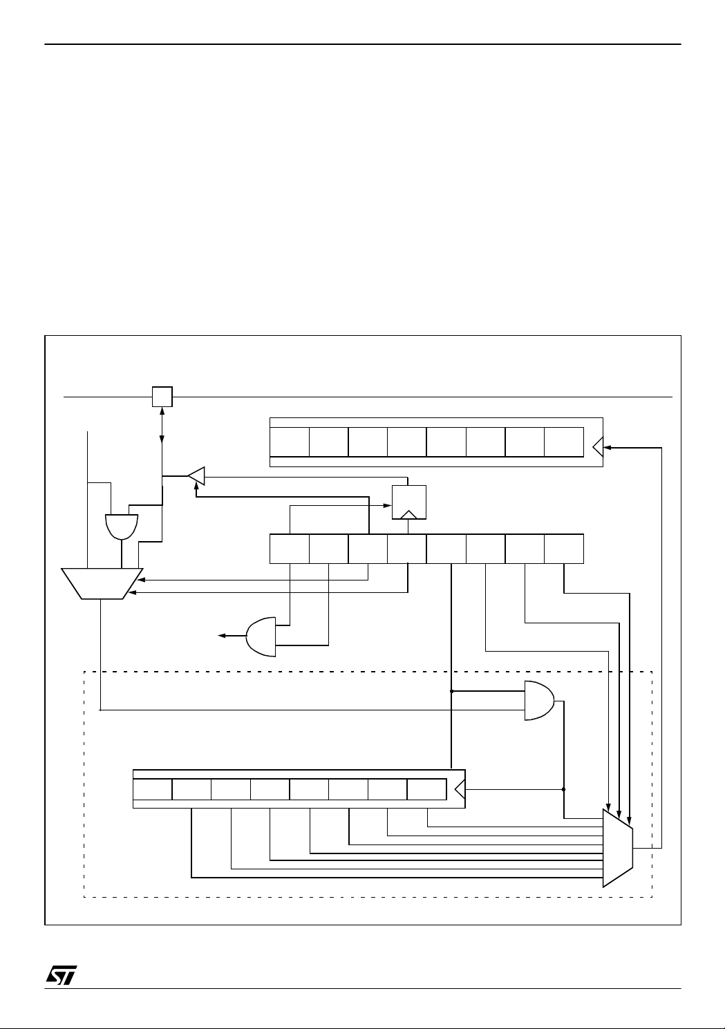
9.2 8-BIT TIMER
ST6215C/ST6225C
9.2.1 Introd uct i on
The 8-Bit Timer on-chip peripheral is a free running downcounter based on an 8-bit downcounter
with a 7-bit programmable prescaler, giving a maximum count of 2
15
. The peripheral may be config-
ured in three different operating modes.
Figure 27. Timer Block Diagram
TIMER
PIN
f
INT/12
f
TCR
REGISTER
EXT
70
TCR7
TCR6 TCR5 TCR4 TCR3 TCR2 TCR1 TCR0
9.2.2 Main Features
■ Time-out downcounting mode with up to 15-bit
accuracy
■ External counter clock source (valid also in
STOP mode)
■ Interrupt capability on counter underflow
■ Output signal generation
■ External pulse length measurement
■ Event counter
The timer can be used in WAIT and S TOP m odes
to wake up the MCU.
8-BIT D O WN COUNTER
LATCH
f
COUNTER
INTERRUPT
7
PSCR6
PSCR7
PROGRAMMABLE PRESCALER
PSCR5 PSCR4 PSCR3 PSCR2 PSCR1 PSCR0
70
ETI TOUT DOUT PSI PS2 PS1 PS0
TMZ
f
PRESCALER
PSCR REGISTER
RELOAD
0
/2
/4/8/16/32/64/128
TSCR
REGISTER
/1
47/105
1
Page 48

ST6215C/ST6225C
8-BI T TIMER (Cont’d)
9.2.3 Counter/Prescaler Description
Prescaler
The prescaler input can be the internal frequency
f
divided by 12 or an external clock applied to
INT
the TIMER pin. The prescaler d ecrements on the
rising edge, depending on the division factor programmed by the PS[2:0] bits in the TSCR register.
The state of the 7-bit prescaler can be read in the
PSCR register.
When the prescaler reaches 0, it is automa tically
reloaded with 7Fh.
Counter
The free running 8-bit downcounter is fed by the
output of the programmable prescaler, and is decremented on every rising edge of the f
clock signal coming from the prescaler.
It is possible to read or write the content s of the
counter on the fly, by reading or writing the timer
counter register (TCR).
When the downcounter reach es 0, it is automatically reloaded with the value 0FFh.
Counter Clock and Prescaler
The counter clock frequency is given by:
where f
–f
INT
–f
EXT
–f
INT
f
COUNTER
PRESCALER
/12
(input on TIMER pin)
/12 gated by TIMER pin
= f
PRESCALER
can be:
/ 2
The timer input clock feeds the 7-bit programmable prescaler. The prescaler output can be programmed by selecting one of the 8 available prescaler taps using the PS[2:0] bits i n t he St atus/Control Register (TSCR). Thus the division factor of
the prescaler can be set to 2
n
(where n equals 0, to
7). See Figure 27.
The clock input is enabled by the PSI (Prescaler
Initialize) bit in the TSCR register. When PSI is reset, the counter is frozen and the prescaler is loaded with the value 7Fh. When PSI is set, the pres-
COUNTER
PS[2:0]
caler and the counter run at the rat e of the s el ect-
ed clock source.
Counter and Prescaler Initialization
After RESET, the counter and the prescaler are in-
itialized to 0FFh and 7Fh respectively.
The 7-bit prescaler can be initialized to 7Fh by
clearing the PSI bit. Direct write access to the
prescaler is also possible when PSI =1. Then, any
value between 0 and 7Fh can be loaded into it.
The 8-bit counter can be initialized separately by
writing to the TCR register.
9.2.3.1 8-bit Counting and Inte rrupt Capability
on Counter Underflow
Whatever the division factor defined for the pres-
caler, the Timer Counter works as an 8-bit down-
counter. The input clock frequency is user selecta-
ble using the PS[2:0] bits.
When the downcounter decrements to zero, the
TMZ (Timer Zero) bit in the TSCR is set. If the ETI
(Enable Timer Interrupt) bit in the TSCR is also
set, an interrupt request is generated.
The Timer interrupt can be used to exit the MCU
from WAIT or STOP mode.
The TCR can be written at any time by software to
define a time period ending with an underflow
event, and therefore manage delay or t imer func-
tions.
TMZ is set when the dow ncounter reaches zero;
however, it may also be set by writing 00h in the
TCR register or by setting bit 7 of the TSCR register.
The TMZ bit must be cleared by user software
when servicing the timer interrupt to avoid unde-
sired interrupts when leaving the interrupt service
routine.
Note: A write to the TCR register will predominate
over the 8-bit counter decrement to 00h function,
i.e. if a write and a TCR register decrement to 00h
occur simultaneously, the write will take prece-
dence, and the TMZ bit is not set until the 8-bit
counter underflows again.
48/105
1
Page 49
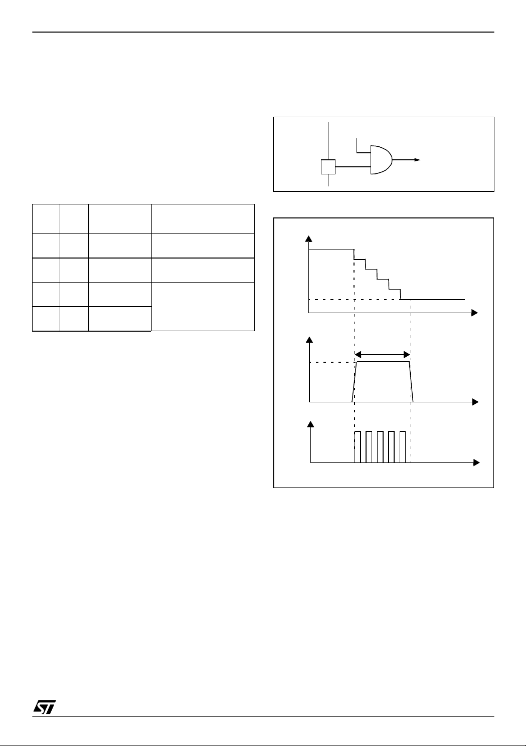
8-BI T TIMER (Cont’d)
9.2.4 Functional Description
There are three operating modes, which are selected by the TOUT and DOUT bits (see TSCR
register). These three modes correspond to the
two clocks which can be connected to the 7-bit
prescaler (f
÷ 12 or TIM ER pin signal), and to
INT
the output mode.
The settings for the different operating modes are
summarized Table 12.
Table 12. Timer Operating Modes
ST6215C/ST6225C
the DDR, OR and DR registers. For more details,
please refer to the I/O Ports section.
Figure 28. f
TIMER
Clock in Gate d Mode
TIMER
f
/12
INT
f
EXT
f
PRESCALER
TOUT DOUT
00
01
10
11
Timer
Function
Event Counter
(input)
Gated input
(input)
Output “0”
(output) Output signal
Output “1”
(output)
Application
External counter clock
source
External Pulse length
measurement
generation
9.2.4.1 Gated Mode
(TOUT = “0”, DOUT = “1”)
In this mode, the prescaler i s dec rem ented by the
Timer clock input, but only when the signa l on th e
TIMER pin is held h igh (f
/12 gated by T IMER
INT
pin). See Figure 28 and Figure 29.
This mode is selected by clearing the TOUT bit in
the TSCR register (i.e. as input) and setting the
DOUT bit.
Note: In this mode, if the TIMER pin is multiplexed, the corresponding port control bits have to
be set in input wi th pull-up configuration through
Figure 29. Ga te d M ode Operation
COUNTER VALUE
VALUE 1
xx1
xx2
TIMER PIN
PULSE LENGTH
1
TIMER CLOCK
VALUE 2
49/105
1
Page 50

ST6215C/ST6225C
8-BI T TIMER (Cont’d)
9.2.4.2 Event Counter Mode
(TOUT = “0”, DOUT = “0”)
In this mode, the TIM ER pin is the input clock of
the Timer prescaler which is decremented on every rising edge of the input clock (allowing event
count). See Figure 30 and Figure 31.
This mode is selected by clearing the TOUT bit in
the TSCR register (i.e. as input) and clearing the
DOUT bit.
Note: In this mode, if the TIMER pin is multiplexed, the corresponding port control bits have to
be set in input with pull-up configuration.
Figure 30. f
Clock in Event Counter Mode
TIMER
f
PRESCALERTIMER
bit transition is used to latch the DOUT bit in the
TSCR and, if the TOUT bit is set, DOUT is trans-
ferred to the TIMER pin. This operating mode allows
external signal generation on the TIMER pin. See
Figure 33.
This mode is selected by s etting the TOUT bit in
the TSCR register (i.e. as output) and s etting the
DOUT bit to output a high level or clearing the
DOUT bit to output a low level.
Note: As soon as the TOUT bit is set , The timer
pin is configured as output push-pull regardless of
the corresponding I/O port control registers setting
(if the TIMER pin is multiplexed).
Figure 32. Output Mode Control
TIMER
LATCH
Figure 31. Event Counter Mode Operation
COUNTER VALUE
VALUE 1
XX1
XX2
TIMER PIN
VALUE 2
9.2.4.3 Output Mode
(TOUT = “1”, DOUT = “data out”)
In Output mode, the TIMER pin is connected to the
DOUT latch, hence the Timer prescaler is clocked
by the prescaler clock input (f
/12). See Figure 32.
INT
The user can select the prescaler division ratio using the PS[2:0] bits in the TSCR register. When TCR
decrements to zero, it sets the TMZ bit i n the TSCR.
The TMZ bit can be tested under program control to
perform a timer function whenever it goes high and
has to be cleared by the user. The low-to-high TMZ
TMZ
TOUT
Figure 33. Output Mode Operation
Counter
FFh
TIMER PIN
1
1st downcount:
Default output value is 0
At each zero event
DOUT has to be
copied to the TIMER
pin
DOUT
50/105
1
Page 51

8-BI T TIMER (Cont’d)
9.2.5 Low Power Modes 9.2.6 Interrupts
Mode Description
WAIT
STOP
No effect on timer.
Timer interrupt events cause the device to
exit from WAIT mode.
Timer registers are frozen except in Event
Counter mode (with external clock on TIMER pin).
Interrupt Event
Timer Zero
Event
ST6215C/ST6225C
Event
Flag
TMZ ETI Yes Yes
Enable
Bit
Exit
from
Wait
Exit
from
Stop
51/105
1
Page 52

ST6215C/ST6225C
8-BI T TIMER (Cont’d)
9.2.7 Register Description
PRESCALER COUNTER REGISTER (PSCR)
Address: 0D2h - Read/Write
Reset Value: 0111 1111 (7Fh)
ETI=0 the timer interrupt i s di sa bled. If ET I=1 and
TMZ=1 an interrupt request is generated.
0: Interrupt disabled (reset state)
1: Interrupt enabled
70
PSCR7PSCR6PSCR5PSCR4PSCR3PSCR2PSCR1PSCR
0
Bit 5 = TOUT Timer Output Control
When low, this bit sel ects the input mode for the
TIMER pin. When high the ou tput mode i s selected.
Bit 7 = PS CR7: Not used, always read as “0”.
Bits 6:0 = PSCR[6:0]
Prescaler LSB.
TIMER COUNTER REGISTER (TCR)
Address: 0D3h - Read / Write
Reset Value: 1111 1111 (FFh)
70
TCR7 TCR6 TCR5 TCR4 TCR3 TCR2 TCR1 TCR0
0: Input mode (reset state)
1: Output mode, t he TIMER pin is configured as
push-pull output
Bit 4 = DOUT
Data Output.
Data sent to the timer output when TMZ is set high
(output mode only). Input mode selection (input
mode only).
Bit 3 = PSI:
Presca ler Ini tialize bit.
Used to initialize the prescaler and inhibit its counting. When PSI=“0” t he presc aler is set to 7Fh and
Bits 7:0 = TCR[7:0]
Timer counter bits.
the counter is inhibited. When PSI=“1” the prescaler is enabled to count downwards. As long as
PSE=“1” both counter and prescaler are not run-
TIMER STATUS CONTROL REGISTER (TSCR)
Address: 0D4h - Read/Write
Reset Value: 0000 0000 (00h)
70
TMZ ETI TOUT DOUT PSI PS2 PS1 PS0
ning
0: Counting disabled
1: Counting enabled
Bits 1:0 = PS[2:0]
Prescaler Mux. Select.
These bits select the division ratio of the prescaler
register.
Bit 7 = TMZ
A low-to-high transition indicates that the timer
count register has underflowed. It means that th e
TCR value has changed from 00h to FFh.
This bit must be cleared by user software.
0: Counter has not underflowed
1: Counter underflow occurred
Bit 6 = ETI
When set, enables the timer interrupt request. If
Timer Zero bit .
Enable Timer Interrupt.
Table 13. Prescaler Division Factors
PS2 PS1 PS0 Divided by
0 0 0 1
0 0 1 2
0 1 0 4
0118
10016
10132
11064
111128
.
Table 14. 8-Bit Timer Register Map and Reset Values
Address
(Hex.)
0D2h
0D3h
0D4h
52/105
Register Label 7 6543210
PSCR
Reset Value
TCR
Reset Value
TSCR
Reset Value
PSCR70PSCR61PSCR51PSCR41PSCR31PSCR21PSCR11PSCR0
TCR71TCR61TCR51TCR41TCR31TCR21TCR11TCR0
TMZ
0
ETI
0
TOUT0DOUT
1
1
1
PSI
0
0
PS2
0
PS1
0
PS0
0
Page 53
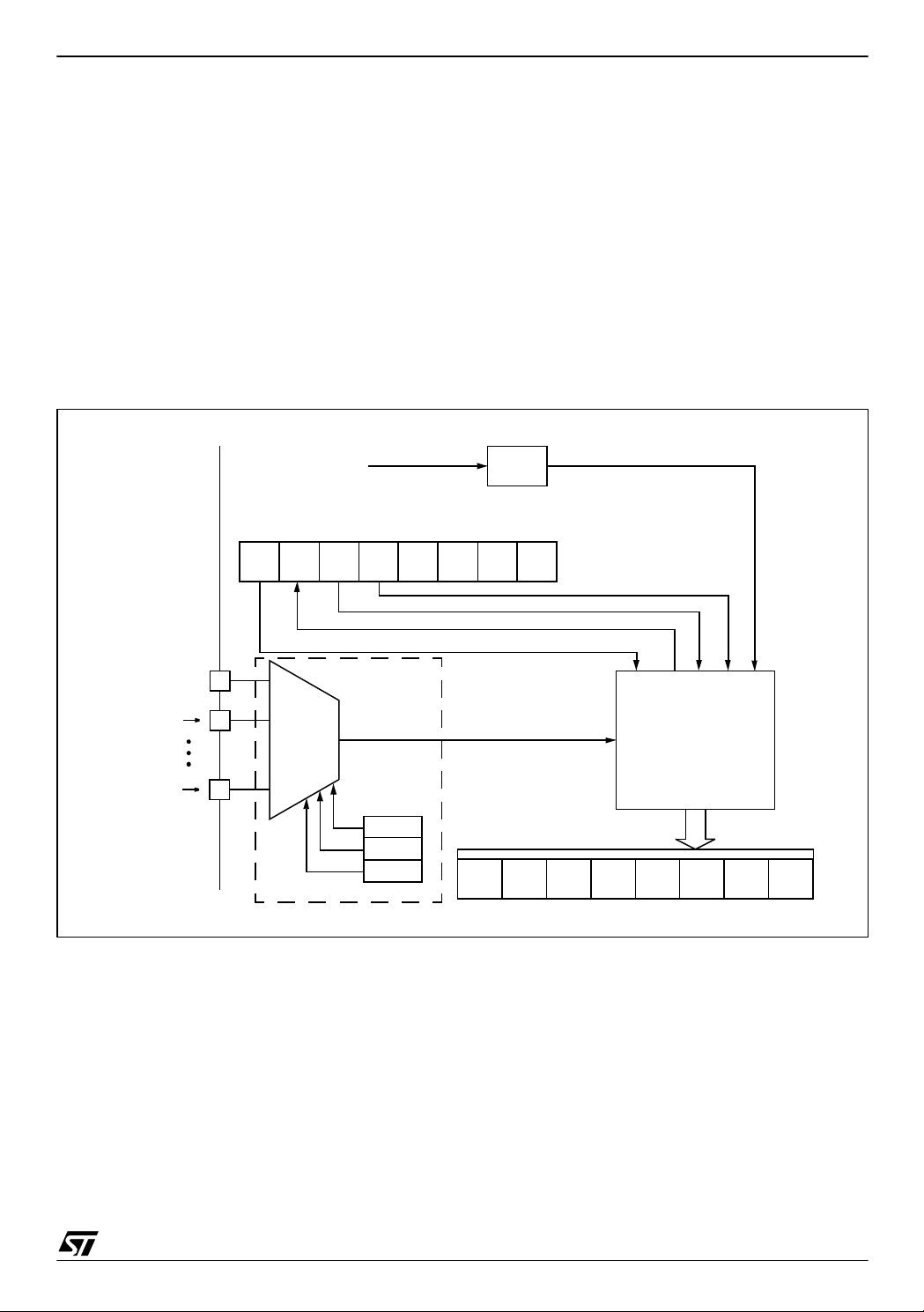
9.3 A/D CONVERTER (ADC)
ST6215C/ST6225C
9.3.1 Introd uct i on
The on-chip Analog to Digital Converter ( ADC) peripheral is a 8-bit, successive approximation converter. This peripheral has multiplexed analog input channels (refer to device pin out description)
that allow the peripheral to convert the analog voltage levels from different sources.
The result of the conversion is stored in a 8-bit
Data Register. The A/D converter is controlled
through a Control Register.
Figure 34. ADC Block Diagram
f
INT
EAI EOC STA PDS
AD
CR3
9.3.2 Main Features
■ 8-bit conversion
■ Multiplexed analog input channels
■ Linear successive approximation
■ Data register (DR) which contains the results
■ End of Conversion flag
■ On/Off bit (to reduce consumption)
■ Typical conversion time 70 µs (with an 8 M Hz
crystal)
The block diagram is shown in Figure 34.
f
ADC
OSC
OFF
DIV 12
AD
CR1ADCR0
ADCR
AIN0
AIN1
AINx
PORT
MUX
I/O PORT
DDRx
ORx
DRx
ADR
ANALOG TO DIGITAL
CONVERTER
ADR2
ADR1ADR3ADR7 ADR6 ADR5 ADR4 ADR0
53/105
1
Page 54

ST6215C/ST6225C
A/D CONVERTER (Cont’d)
9.3.3 Functional Description
9.3.3.1 Analog Power Supply
The high and low level reference voltage pi ns are
internally connected to the V
Conversion accuracy may therefore be impacted
by voltage drops and noise in the event of heavily
loaded or badly decoupled power supply lines.
9.3.3.2 Digital A/D Conversion Result
The conversion is monotonic, meaning that the result never decreases if t he analog i nput does not
and never increases if the analog input does not.
If the input voltage (V
to V
(high-level voltage reference) then the
DDA
AIN
conversion result in the DR register is FFh (full
scale) without overflow indication.
If input voltage (V
V
(low-level voltage reference) then the con-
SSA
) is lower than or equal to
AIN
version result in the DR register is 00h.
The A/D converter is linear and the digital result of
the conversion is stored in the ADR regi ster. The
accuracy of the conversion is described in the parametric section.
is the maximum recommended impedance
R
AIN
for an analog input signal. If the impedance is too
high, this will result in a loss of accuracy due to
leakage and sampling not being completed in the
allocated time. Refer to the electrical characteristics chapter for more details.
With an oscillator clock frequency less than
1.2MHz, conversion accuracy is decreased.
9.3.3.3 Analog Input Selection
Selection of the input pi n is done by configuring
the related I/O line as an analog input via the Data
Direction, Option and Data registe rs (refer to I/O
ports description for additional information).
Caution: Only one I/O line m ust be c onf igured as
an analog input at any time. T he us er must av oid
any situation in which more than one I/O pin is selected as an analog input simultaneously, because
they will be shorted internally.
and VSS pins.
DD
) is greater than or equal
9.3.3.4 Software Procedure
Refer to the Control register (ADCR) and Data register (ADR) in Section 9.3.7 for the bit definitions.
Analog Input Configuration
The analog inpu t must be con figured through t he
Port Control registers (DDRx, ORx and DRx). Refer to the I/O port chapter.
ADC Configuration
In the ADCR register:
– Reset the PDS bit to power on the ADC. This bit
must be set at least one instruction before the
beginning of the conversion to allow stabilisation
of the A/D converter.
– Set the EAI bit to enable the ADC interrupt if
needed.
ADC Conversion
In the ADCR register:
– Set the STA bit to start a conversion. This auto-
matically clears (resets to “0”) the End Of Con-
version Bit (EOC).
When a conversion is complete
– The EOC bit is set by hardware to flag that con-
version is complete and that the data in the ADC
data conversion register is valid.
– An interrupt is generated if the EAI bit was set
Setting the STA bit will start a new count and will
clear the EOC bit (thus clearing the interrupt condition)
Note:
Setting the STA bit must be done by a different instruction from the instruction that powers-on the
ADC (setting the PDS bit) in order to m ake sure
the voltage to be converted is present on the pin.
Each conversion has to be separately initiated by
writing to the STA bit.
The STA bit is continuously scanned so that, if the
user sets it to “1” while a previous conversion is in
progress, a new conversion is started before completing the previous one. The start bit (STA) is a
write only bit, any attempt to read it will show a logical “0”.
54/105
1
Page 55

A/D CONVERTER (Cont’d)
9.3.4 Recommendations
The following six notes provide additional information on using the A/D converter.
1.The A/D converter does not feature a sample
and hold circuit. The an alog voltage to be m easured should therefore be stable during the entire
conversion cycle. Voltage variation should not exceed ±1/2 LSB for optimum conversion accuracy.
A low pass filter may be used at the analog input
pins to reduce input voltage variation during conversion.
2. When selected as an analog channel, the i nput
pin is internally connected to a capacitor C
typically 9p F. For maximum accu racy, this capaci-
ad
of
tor must be fully cha rged at the beginning of conversion. In the worst case, conversion starts one
instruction (6.5 µs) after the channel has been selected. The impedance of the analog voltage
source (ASI) in worst case conditions, is calculated using the following formula:
6.5µs = 9 x C
x ASI
ad
(capacitor charged to over 99.9%), i.e. 30 kΩ including a 50% guardband.
The ASI can be higher if C
has been charged for
ad
a longer period by adding instructions before the
start of conversion (adding more than 26 CP U cy cles is pointless).
3. Since the ADC is on the same chip as t he microprocessor, the user should not switch heavily loaded output signals during conversion, if high precision is required. Such switching will affect the supply voltages used as analog references.
4. Conversion accuracy depends on the quality of
the power supplies (V
and VSS). The user must
DD
take special care to ensure a well regulated reference voltage is present on t he V
and VSS pins
DD
(power supply voltage variations must be less than
0.1V/ms). This implies, in particular, that a suitable
decoupling capacitor is used at the V
DD
pin.
The converter resolution is given by:
V
–
DDVSS
------------------------------- 256
The Input voltage (Ain) which is to be converted
must be constant for 1µs before conversion and
remain constant during conversion.
5. Conversion resolution can be improved if the
power supply voltage (V
) to the mi crocontroller
DD
is lowered.
6. In order to optimize the conversion resolution,
the user can configure the microcontroller in WAIT
mode, because this mode minimises noise dist ur-
ST6215C/ST6225C
bances and power supply variation s due to ou tput
switching. Nevertheless, the WAIT instruction
should be execut ed as s oon as possible after the
beginning of the conversion, because execution of
the WAIT instruction may cause a small variation
of the V
iation is minimized at the b eginning of the conversion when the converter is less sensitive, rather
than at the end of conversion, when the leas t significant bits are determined.
The best configuration, from an accuracy standpoint, is WAIT mode with the Timer stopped. In
this case only the ADC peripheral and the oscillator are then still working. The MCU must be woken
up from WAIT mode by the ADC interrupt at the
end of the conversion. The microcontroller can
also be woken up by the Timer interrupt, but this
means the Timer must be running an d the resulting noise could affect conversion accuracy.
Caution: When an I/O pin is used as an analog input, A/D conversion accuracy will be impaired if
negative current injections (V
adjacent I/O pi ns w ith analog input capability. Refer to Figure 35. To avoid this:
– Use another I/O port located further away from
the analog pin, preferably not multiplexed on the
A/D converter
– Increase the input resistance R
current injections) and reduce R
conversion accuracy).
Figure 35. Leakage from Digital Inputs
voltage. The negative effect of this var-
DD
< VSS) occur from
INJ
IN J
ADC
Digital
Input
R
INJ
V
INJ
PBy/AINy
Leakage Current
if V
INJ
< V
Analog
Input
R
ADC
V
AIN
PBx/AINx
(to reduce the
(to preserve
I/O Port
(Digital I/O)
SS
A/D
Converter
55/105
1
Page 56

ST6215C/ST6225C
A/D CONVERTER (Cont’d)
9.3.5 Low Power Modes
Mode Description
WAIT
STOP A/D Converter disabled.
Note: The A/D converter may be disabled by clearing the PDS bit. This feature allows reduced power
consumption when no conversion is needed.
9.3.6 Interrupts
Interrupt Event
End of Conversion
Note: The EOC bit is cleared only when a new
conversion is started (it cannot be cleared by writing 0). To avoid generating further EOC interrupt,
the EAI bit has to be cleared within the ADC interrupt subroutine.
9.3.7 Register Description
A/D CONVERTER CONTROL REGISTER (AD-
CR)
Address: 0D1h - Read/Write (Bit 6 Read Only, Bit
5 Write Only)
Reset value: 0100 0000 (40h)
No effect on A/D Converter. ADC interrupts
cause the device to exit from Wait mode.
Event
Flag
EOC EAI Yes No
Enable
Bit
Exit
from
Wait
Exit
from
Stop
cally cleared when the STA bit is set . Data in the
data conversion register are valid only when this
bit is set to “1”.
0: Conversion is not complete
1: Conversion can be read from the ADR register
Bit 5 = STA
: Start of Conversion. Write Only
.
0: No effect
1: Start conversion
Note: Setting this bit automatically clears the EOC
bit. If the bit is set again when a conversion is in
progress, the present conversion is stopped and a
new one will take place. This bit is write only, any
attempt to read it will show a logical zero.
Bit 4 = PDS
Power Down Selection.
0: A/D converter is switched off
1: A/D converter is switched on
Bit 3 = ADCR3 Reserved, must be cleared.
Bit 2 = OSCOFF
Main Oscillator off.
0: Main Oscillator enabled
1: Main Oscillator disabled
Note: This bit does not apply to the ADC peripheral but to th e main clock system. Refer to the Clock
System section.
70
EAI EOC STA PDS
ADCR3OSC
OFF
ADCR1ADCR
0
Bits 1:0 = ADCR[1:0] Reserved, must be cleared.
A/D CONVERTER DATA REGISTER (ADR)
Bit 7 = EAI
0: ADC interrupt disabled
1: ADC interrupt enabled
Bit 6 = EOC
When a conversion has been completed, this bit is
Enable A/D Interrupt.
End of conversion. Read Only
Address: 0D0h - Read only
Reset value: xxxx xxxx (xxh)
70
ADR7 ADR6 ADR5 ADR4 ADR3 ADR2 ADR1 ADR0
set by hardware and an interrupt request is generated if the EAI bit is set. The EOC bit is automati-
Bits 7:0 = ADR[7:0]
: 8 Bit A/D Conversion Result.
Table 15. ADC Register Map and Reset Values
Address
(Hex.)
0D0h
0D1h
56/105
Register
Label
ADR
Reset Value
ADCR
Reset Value
76543210
ADR7
0
EAI
0
ADR6
0
EOC
1
ADR5
0
STA
0
ADR4
0
PDS
0
ADR3
0
ADCR30OSCOFF0ADCR10ADCR0
ADR2
0
ADR1
0
ADR0
0
0
1
Page 57

10 INSTRUCTIO N SET
10.1 ST6 ARCHITECTURE
ST6215C/ST6225C
The ST6 architecture has been designe d for max imum efficiency while keeping byte usage to a
minimum; in short, to provide byte-efficient programming. The ST6 core has the abi lity to set or
clear any register or RAM location bit in Data
space using a single instruction. Furthermore, programs can branch to a selected address depending on the status of any bit in Data space.
10.2 ADDRESSING MODES
The ST6 has nine addressing mo des, which are
described in the following paragraphs. Three different address spaces are available: Program
space, Data space, and Stack space. Program
space contains the instructions which are to be executed, plus the data for immedi ate mo de in structions. Data space contains the Accumulator, the X,
Y, V and W registers, peripheral and Input/Output
registers, the RAM lo cations and Data ROM loc ations (for storage of tables and constants). Stack
space contains six 12-bi t RA M cells used t o st ack
the return addresses for subroutines and interrupts.
Immediate. In immediate addressing mode, the
operand of the instruction follows the opcode location. As the operand is a ROM byte, the immediate
addressing mode is used to access constants
which do not change during program execution
(e.g., a constant used to initialize a loop counter).
Direct. In direct addressing mode , the address of
the byte which is proc essed by the instruction is
stored in the location which follows the opcode. Direct addressing allows the user to directly address
the 256 bytes in Data Space memory with a single
two-byte instruction.
Short Direct. The core can address the four RAM
registers X, Y, V, W (locations 80h, 81h, 82h, 83h)
in short-direct addressing mode. In this case, the
instruction is only one byte and the selection of the
location to be processed is contained in the opcode. Short direct addressing is a subset of direct
addressing mode. (Note that 80h and 81h are also
indirect registers).
tended addressing mode are able to branch to any
address in the 4 Kbyte Program space.
Extended addressing mode instructions are two
bytes long.
Program Counter Relative. Relative addressing
mode is only us ed in conditional branch instructions. The instruction is used to perform a test and,
if the condition is true, a branch with a span of -15
to +16 locations next to the address of the relative
instruction. If the condition is not true, the instructio n w h ic h fo l lo ws t he rela t iv e i ns truct i o n is e x ec ut ed. Relative addressing mode instructions are one
byte long. The opcode is obtained by adding the
three most significant bits which characterize the
test condition, one bit which determines whether it
is a forward branch (when it is 0) or backward
branch (when it is 1) and the four least significant
bits which give the span of t he branch (0h t o Fh)
which must be added or subtracted from the address of the relative instruction to obtain the
branch destination address.
Bit Direct. In bit direct addressing mode, the bit to
be set or cleared is pa rt of the opcode, and the
byte following the opcod e poin ts to t he add ress of
the byte in which the specified bit must be set or
cleared. Thus, any bit in the 25 6 locat ions of Data
space memory can be set or cleared.
Bit Test & Branch. Bit test and branch addressing
mode is a combination of direct addressing and
relative addressing. Bit test and branch instructions are three bytes long. The bit identification
and the test c ondition are include d in the opcode
byte. The address of the byte to be tested is given
in the next byte. The third byte is the jump displacement, which is in the range of -127 to +128.
This displacement can be determ ined using a label, which is converted by the assembler.
Indirect. In indirect addressing mode, the byte
processed by the register-indirect instruction is at
the address pointed to by the content of one of the
indirect registers, X or Y (80h, 81h). The indirect
register is selected by bit 4 of the opcode. Register
indirect instructions are one byte long.
Extended. In extended addressing mode, the 12bit address needed to define the instruction is obtained by concatenating the four least significant
bits of the opcode with the byte following the opcode. The instructions (JP, CALL) which use ex-
Inherent. I n inherent addres sing mo de, all the information necessary for executing t he instruction
is contained in the opcode. These i nstructions are
one byte long.
57/105
1
Page 58

ST6215C/ST6225C
10.3 INSTRUCTION SET
The ST6 offers a set of 40 basic instructions
which, when combined with nine addressing
modes, yield 244 usable opcodes. They can be divided into six different ty pes: load/store, arithmetic/logic, conditional branch, control instructions,
jump/call, and bit manipu lat ion. T he f ollowing paragraphs describe the different types.
All the instructions belonging to a given type are
Load & Store. These instructions use one, two or
three bytes depending on the addressing mode.
For LOAD, one operand is the Accumulator and
the other operand i s obtained from dat a memory
using one of the addressing modes.
For Load Immediate, on e operand can be any of
the 256 data space bytes while the other is always
immediate data.
presented in individual tables.
Table 16. Load & Store Instructions
Instruction Addressing Mode Bytes Cycles
LD A, X Short Direct 1 4 ∆ *
LD A, Y Short Direct 1 4 ∆ *
LD A, V Short Direct 1 4 ∆ *
LD A, W Short Direct 1 4 ∆ *
LD X, A Short Direct 1 4 ∆ *
LD Y, A Short Direct 1 4 ∆ *
LD V, A Short Direct 1 4 ∆ *
LD W, A Short Direct 1 4 ∆ *
LD A, rr Direct 2 4 ∆ *
LD rr, A Direct 2 4 ∆ *
LD A, (X) Indirect 1 4 ∆ *
LD A, (Y) Indirect 1 4 ∆ *
LD (X), A Indirect 1 4 ∆ *
LD (Y), A Indirect 1 4 ∆ *
LDI A, #N Immediate 2 4 ∆ *
LDI rr, #N Immediate 3 4 * *
Flags
ZC
Legend:
X, Y Index Reg i st ers,
V, W Short Direct Registers
# Immedi at e data (stored in ROM memory)
rr Data spac e register
∆ Affected
* Not Affected
58/105
1
Page 59

INSTRUCTION SET (Cont’d)
ST6215C/ST6225C
Arithmetic and Logic. These instructions are
used to perform arithmetic calculations and logic
operations. In AND, ADD, CP, SUB instructions
one operand is always the accumulator while, depending on the addressing mode, the other can be
either a data spa ce memory location or an immediate value. In CLR, DEC, INC instructions the operand can be any of the 256 data space add resses. In COM, RLC, SLA the operan d is always the
accumulator.
Table 17. Arithmetic & Logic Instructions
Instruction Addressing Mode Bytes Cycles
ADD A, (X) Indirect 1 4 ∆∆
ADD A, (Y) Indirect 1 4 ∆∆
ADD A, rr Direct 2 4 ∆∆
ADDI A, #N Immediate 2 4 ∆∆
AND A, (X) Indirect 1 4 ∆∆
AND A, (Y) Indirect 1 4 ∆∆
AND A, rr Direct 2 4 ∆∆
ANDI A, #N Immediate 2 4 ∆∆
CLR A Short Direct 2 4 ∆∆
CLR r Direct 3 4 * *
COM A Inherent 1 4 ∆∆
CP A, (X) Indirect 1 4 ∆∆
CP A, (Y) Indirect 1 4 ∆∆
CP A, rr Direct 2 4 ∆∆
CPI A, #N Immediate 2 4 ∆∆
DEC X Short Direct 1 4 ∆ *
DEC Y Short Direct 1 4 ∆ *
DEC V Short Direct 1 4 ∆ *
DEC W Short Direct 1 4 ∆ *
DEC A Direct 2 4 ∆ *
DEC rr Direct 2 4 ∆ *
DEC (X) Indirect 1 4 ∆ *
DEC (Y) Indirect 1 4 ∆ *
INC X Short Direct 1 4 ∆ *
INC Y Short Direct 1 4 ∆ *
INC V Short Direct 1 4 ∆ *
INC W Short Direct 1 4 ∆ *
INC A Direct 2 4 ∆ *
INC rr Direct 2 4 ∆ *
INC (X) Indirect 1 4 ∆ *
INC (Y) Indirect 1 4 ∆ *
RLC A Inherent 1 4 ∆∆
SLA A Inherent 2 4 ∆∆
SUB A, (X) Indirect 1 4 ∆∆
SUB A, (Y) Indirect 1 4 ∆∆
SUB A, rr Direct 2 4 ∆∆
SUBI A, #N Immediate 2 4 ∆∆
Notes:
X,Y Index Registers
V, W Short Di rect Registers
∆ Affected
# Immediate data (stored in ROM memory)
* Not Affected
rr Da ta space regist er
Flags
ZC
59/105
1
Page 60

ST6215C/ST6225C
INSTRUCTION SET (Cont’d)
Conditional Branch. Branch instructions perform
a branch in the program wh en the s elected condition is met.
Bit Manipulation Instructions. These instructions can handle any bit in Data space memory.
One group either sets or clears. The ot her group
Control Instru ctions. Control instructions control
microcontroller operations during program execution.
Jump and Call. These two instructions are used
to perform long (12-bit) jumps or subroutine calls
to any location in the whole program space.
(see Conditional Branch) performs the bit test
branch operations.
Table 18. Conditional Branch Instructions
Instruction Branch If Bytes Cycles
JRC e C = 1 1 2 * *
JRNC e C = 0 1 2 * *
JRZ e Z = 1 1 2 * *
JRNZ e Z = 0 1 2 * *
JRR b, rr, ee Bit = 0 3 5 * ∆
JRS b, rr, ee Bit = 1 3 5 * ∆
Notes:
b 3-bit address rr Data space register
e 5 bit signed dis pl acement in the range -15 to +16 ∆ Affected. The tested bit is shifted into carry.
ee 8 bit signed displacement in th e range -126 to +129 * Not Affected
Flags
ZC
Table 19. Bit Manipulation Instructions
Instruction Addressing Mode Bytes Cycles
SET b,rr Bit Direct 2 4 * *
RES b,rr Bit Direct 2 4 * *
Notes:
b 3-bit addre ss * Not Affe ct ed
rr Data space r egi ster
Bit Manipul ation Instructions sho u l d not be used on Port Data Registers and any registers with rea d only and/or write only bits (see I/O p ort
chapter)
Flags
ZC
Table 20. Control Instructio ns
Instruction Addressing Mode Bytes Cycles
NOP Inherent 1 2 * *
RET Inherent 1 2 * *
RETI Inherent 1 2 ∆∆
(1)
STOP
WAIT Inherent 1 2 * *
Notes:
1. This instru ct i on i s deactivated and a WAIT is autom atically executed instead of a STOP if the wat chdog functio n i s s el ected.
∆ Affected *Not Affected
Inherent 1 2 * *
Flags
ZC
Table 21. Jump & Call Instructions
Instruction Addressing Mode Bytes Cycles
CALL abc Extended 2 4 * *
JP abc Extended 2 4 * *
Notes:
abc 12-bit address
* N ot Affected
Flags
ZC
60/105
1
Page 61

ST6215C/ST6225C
Opcode Map Summary. The following table contains an opcode map for the instructions used by the ST6
LOW
HI HI
0
0000
1
0001
2
0010
3
0011
4
0100
5
0101
6
0110
7
0111
8
1000
9
1001
A
1010
B
1011
C
1100
D
1101
E
1110
F
1111
0
0000
2 JRNZ 4 CALL 2 JRNC 5 JRR 2 JRZ 2 JRC 4 LD
e abc e b0,rr,ee e NOP # e a,(x)
1pcr2ext1pcr3 bt1pcr 1prc1ind
2 JRNZ 4 CALL 2 JRNC 5 JRS 2 JRZ 4 INC 2 JRC 4 LDI
e abc e b0,rr,ee e x e a,nn
1pcr2ext1pcr3 bt1pcr1 sd1prc2imm
2 JRNZ 4 CALL 2 JRNC 5 JRR 2 JRZ 2 JRC 4 CP
e abc e b4,rr,ee e # e a,(x)
1pcr2ext1pcr3 bt1pcr 1prc1ind
2 JRNZ 4 CALL 2 JRNC 5 JRS 2 JRZ 4 LD 2 JRC 4 CPI
e abc e b4,rr,ee e a,x e a,nn
1pcr2ext1pcr3 bt1pcr1 sd1prc2imm
2 JRNZ 4 CALL 2 JRNC 5 JRR 2 JRZ 2 JRC 4 ADD
e abc e b2,rr,ee e # e a,(x)
1pcr2ext1pcr3 bt1pcr 1prc1ind
2 JRNZ 4 CALL 2 JRNC 5 JRS 2 JRZ 4 INC 2 JRC 4 ADDI
e abc e b2,rr,ee e y e a,nn
1pcr2ext1pcr3 bt1pcr1 sd1prc2imm
2 JRNZ 4 CALL 2 JRNC 5 JRR 2 JRZ 2 JRC 4 INC
e abc e b6,rr,ee e # e (x)
1pcr2ext1pcr3 bt1pcr 1prc1ind
2 JRNZ 4 CALL 2 JRNC 5 JRS 2 JRZ 4 LD 2 JRC
e abc e b6,rr,ee e a,y e #
1pcr2ext1pcr3 bt1pcr1 sd1prc
2 JRNZ 4 CALL 2 JRNC 5 JRR 2 JRZ 2 JRC 4 LD
e abc e b1,rr,ee e # e (x),a
1pcr2ext1pcr3 bt1pcr 1prc1ind
2 JRNZ 4 CALL 2 JRNC 5 JRS 2 JRZ 4 INC 2 JRC
e abc e b1,rr,ee e v e #
1pcr2ext1pcr3 bt1pcr1 sd1prc
2 JRNZ 4 CALL 2 JRNC 5 JRR 2 JRZ 2 JRC 4 AND
e abc e b5,rr,ee e # e a,(x)
1pcr2ext1pcr3 bt1pcr 1prc1ind
2 JRNZ 4 CALL 2 JRNC 5 JRS 2 JRZ 4 LD 2 JRC 4 ANDI
e abc e b5,rr,ee e a,v e a,nn
1pcr2ext1pcr3 bt1pcr1 sd1prc2imm
2 JRNZ 4 CALL 2 JRNC 5 JRR 2 JRZ 2 JRC 4 SUB
e abc e b3,rr,ee e # e a,(x)
1pcr2ext1pcr3 bt1pcr 1prc1ind
2 JRNZ 4 CALL 2 JRNC 5 JRS 2 JRZ 4 INC 2 JRC 4 SUBI
e abc e b3,rr,ee e w e a,nn
1pcr2ext1pcr3 bt1pcr1 sd1prc2imm
2 JRNZ 4 CALL 2 JRNC 5 JRR 2 JRZ 2 JRC 4 DEC
e abc e b7,rr,ee e # e (x)
1pcr2ext1pcr3 bt1pcr 1prc1ind
2 JRNZ 4 CALL 2 JRNC 5 JRS 2 JRZ 4 LD 2 JRC
e abc e b7,rr,ee e a,w e #
1pcr2ext1pcr3 bt1pcr1 sd1prc
1
0001
2
0010
3
0011
4
0100
5
0101
6
0110
0111
LOW
7
0
0000
1
0001
2
0010
3
0011
4
0100
5
0101
6
0110
7
0111
8
1000
9
1001
A
1010
B
1011
C
1100
D
1101
E
1110
F
1111
Abbreviations for Addressing Modes: Legend:
dir Direct # Indicates Illegal Instructions
sd Short Direct e 5-bit Displacement
imm Immediate b 3-bit Address
inh Inhe rent rr 1-byte Data space address
ext Extended nn 1-byte immediate data
b.d Bit Direct abc 12-bit address
bt Bit Test ee 8-bit displacement
pcr Program Counter Relative
ind Indirect
Cycles
Operands
Bytes
Addressing Mode
2
JRC
e
1prc
Mnemonic
61/105
1
Page 62

ST6215C/ST6225C
Opcode Map Summary (Continued)
LOW
HI HI
0
0000
1
0001
2
0010
3
0011
4
0100
5
0101
6
0110
7
0111
8
1000
9
1001
A
1010
B
1011
C
1100
D
1101
E
1110
F
1111
8
1000
2 JRNZ 4 JP 2 JRNC 4 RES 2 JRZ 4 LDI 2 JRC 4 LD
e abc e b0,rr e rr,nn e a,(y)
1pcr2ext1pcr2b.d1pcr3imm1prc1ind
2 JRNZ 4 JP 2 JRNC 4 SET 2 JRZ 4 DEC 2 JRC 4 LD
e abc e b0,rr e x e a,rr
1pcr2ext1pcr2b.d1pcr1 sd1prc2 dir
2 JRNZ 4 JP 2 JRNC 4 RES 2 JRZ 4 COM 2 JRC 4 CP
e abc e b4,rr e a e a,(y)
1pcr2ext1pcr2b.d1pcr 1prc1ind
2 JRNZ 4 JP 2 JRNC 4 SET 2 JRZ 4 LD 2 JRC 4 CP
e abc e b4,rr e x,a e a,rr
1pcr2ext1pcr2b.d1pcr1 sd1prc2 dir
2 JRNZ 4 JP 2 JRNC 4 RES 2 JRZ 2 RETI 2 JRC 4 ADD
e abc e b2,rr e e a,(y)
1pcr2ext1pcr2b.d1pcr1inh1prc1ind
2 JRNZ 4 JP 2 JRNC 4 SET 2 JRZ 4 DEC 2 JRC 4 ADD
e abc e b2,rr e y e a,rr
1pcr2ext1pcr2b.d1pcr1 sd1prc2 dir
2 JRNZ 4 JP 2 JRNC 4 RES 2 JRZ 2 STOP 2 JRC 4 INC
e abc e b6,rr e e (y)
1pcr2ext1pcr2b.d1pcr1inh1prc1ind
2 JRNZ 4 JP 2 JRNC 4 SET 2 JRZ 4 LD 2 JRC 4 INC
e abc e b6,rr e y,a e rr
1pcr2ext1pcr2b.d1pcr1 sd1prc2 dir
2 JRNZ 4 JP 2 JRNC 4 RES 2 JRZ 2 JRC 4 LD
e abc e b1,rr e # e (y),a
1pcr2ext1pcr2b.d1pcr 1prc1ind
2 JRNZ 4 JP 2 JRNC 4 SET 2 JRZ 4 DEC 2 JRC 4 LD
e abc e b1,rr e v e rr,a
1pcr2ext1pcr2b.d1pcr1 sd1prc2 dir
2 JRNZ 4 JP 2 JRNC 4 RES 2 JRZ 4 RCL 2 JRC 4 AND
e abc e b5,rr e a e a,(y)
1pcr2ext1pcr2b.d1pcr1inh1prc1ind
2 JRNZ 4 JP 2 JRNC 4 SET 2 JRZ 4 LD 2 JRC 4 AND
e abc e b5,rr e v,a e a,rr
1pcr2ext1pcr2b.d1pcr1 sd1prc2 dir
2 JRNZ 4 JP 2 JRNC 4 RES 2 JRZ 2 RET 2 JRC 4 SUB
e abc e b3,rr e e a,(y)
1pcr2ext1pcr2b.d1pcr1inh1prc1ind
2 JRNZ 4 JP 2 JRNC 4 SET 2 JRZ 4 DEC 2 JRC 4 SUB
e abc e b3,rr e w e a,rr
1pcr2ext1pcr2b.d1pcr1 sd1prc2 dir
2 JRNZ 4 JP 2 JRNC 4 RES 2 JRZ 2 WAIT 2 JRC 4 DEC
e abc e b7,rr e e (y)
1pcr2ext1pcr2b.d1pcr1inh1prc1ind
2 JRNZ 4 JP 2 JRNC 4 SET 2 JRZ 4 LD 2 JRC 4 DEC
e abc e b7,rr e w,a e rr
1pcr2ext1pcr2b.d1pcr1 sd1prc2 dir
9
1001
A
1010
B
1011
C
1100
D
1101
E
1110
1111
LOW
F
0
0000
1
0001
2
0010
3
0011
4
0100
5
0101
6
0110
7
0111
8
1000
9
1001
A
1010
B
1011
C
1100
D
1101
E
1110
F
1111
Abbreviations for Addressing Modes: Legend:
dir Direct # Indicates Illegal Instructions
sd Short Direct e 5-bit Displacement
imm Immediate b 3-bit Address
inh Inhe rent rr 1-byte Data space address
ext Extended nn 1-byte immediate data
b.d Bit Direct abc 12-bit address
bt Bit Test ee 8-bit Displacement
pcr Program Counter Relative
ind Indirect
Cycles
Operands
Bytes
Addressing Mode
62/105
1
2
JRC
e
1prc
Mnemonic
Page 63
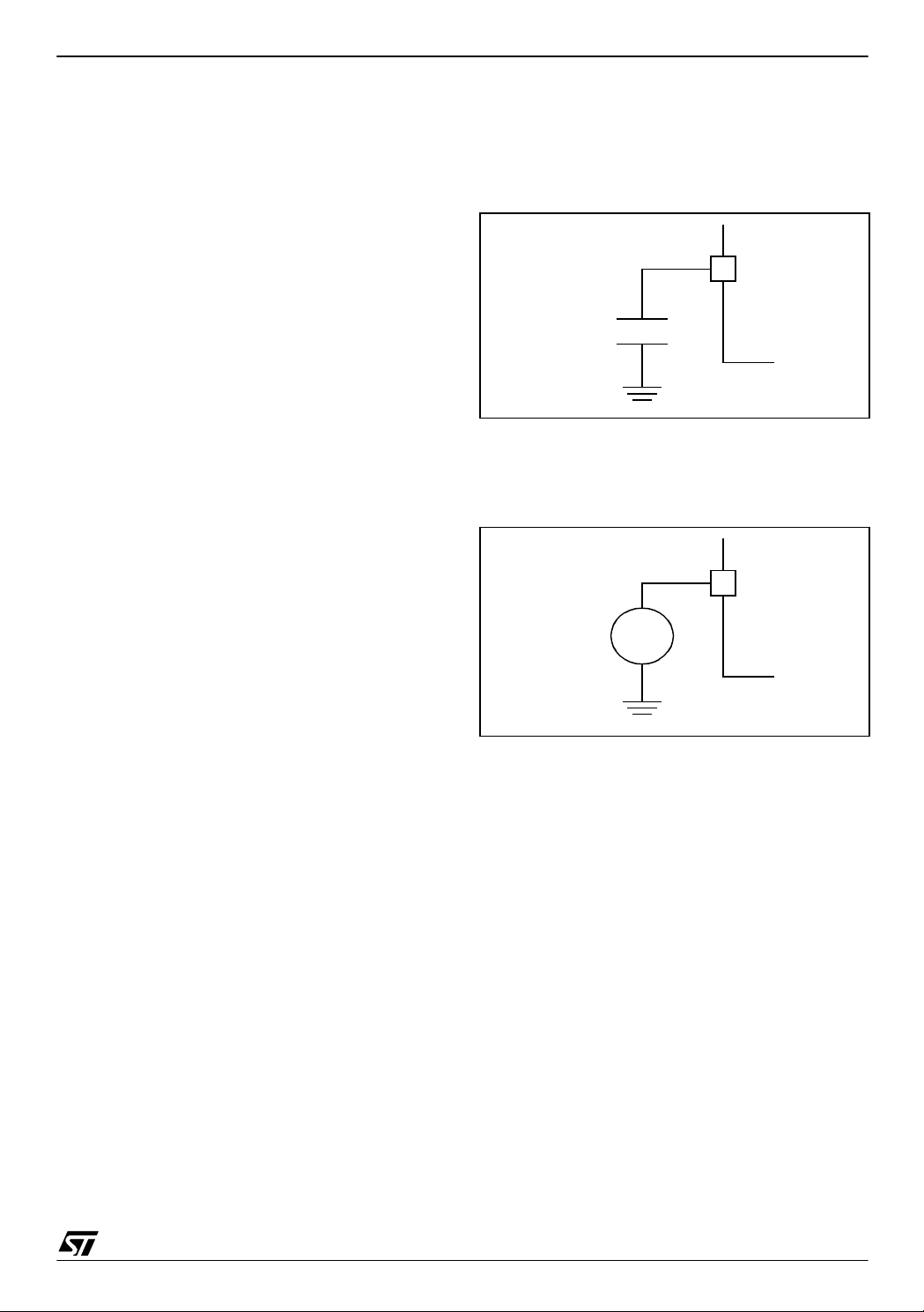
11 ELECTRIC AL CHARACTERISTICS
11.1 PARAMETER CONDITIONS
ST6215C/ST6225C
Unless otherwise specified, all voltages are referred to V
SS
.
11.1.1 Minimum and Maximum Values
Unless otherwise specified the minimum and maximum values are guaranteed in the worst conditions of ambient t emperature, supp ly voltage an d
frequencies by tests in production on 100% of the
devices with an ambient temp erature at T
and T
max (given by the selected temperature
A=TA
=25°C
A
range).
Data based on characterization results, design
simulation and/or technology characteristics are
indicated in the table foo tnotes and are not tested
in production. Based on characterization, the mi nimum and maximum values refer to sample tests
and represent the mean value plus or minus three
times the standard deviation (mean±3Σ).
11.1.2 Typical Values
Unless otherwise specified, typical data are based
on T
=25°C, VDD=5V (for the 4.5V≤VDD≤6.0V
A
voltage range) and V
3V≤V
≤3.6V voltage range). They are given only
DD
=3.3V (for the
DD
as design guidelines and are not tested.
11.1.3 Typical Curves
Unless otherwise specified, all typical curves are
given only as design guidelines and are not tested.
11.1.4 Loading Capacitor
The loading conditions used for pin parameter
measurement is sh own in Figure 36.
Figure 36. Pin Loading Cond itions
ST6 PIN
C
L
11.1.5 Pin Input Voltage
The input voltage measurement on a pin of the device is described in Figure 37.
Figure 37. Pin In put Voltage
ST6 PIN
V
IN
63/105
1
Page 64

ST6215C/ST6225C
11.2 ABSOLUTE MAXIMUM RATINGS
Stresses above those listed as “absolute maximum ratings” may cause permanent damage to
the device. This is a stress rating only and func tional operation of the device under these cond i-
11.2.1 Voltage Characteristics
Symbol Ratings Maximum value Unit
- V
V
DD
V
IN
V
OUT
V
ESD(HBM)
SS
Supply voltage 7
Input voltage on any pin
Output voltage on any pin
1) & 2)
1) & 2)
Electro-static discharge voltage (Human Body Model)
11.2.2 Current Characteristics
Symbol Ratings Maximum value Unit
I
VDD
I
VSS
Total current into VDD power lines (source)
Total current out of VSS ground lines (sink)
Output current sunk by any standard I/O and control pin 20
I
IO
Output current sunk by any high sink I/O pin 40
Output current source by any I/Os and control pin 15
I
INJ(PIN)
2) & 4)
Injected current on RESET pin ±5
Injected current on any other pin
11.2.3 Thermal Characteristics
Symbol Ratings Value Unit
T
STG
T
J
Storage temperature range -60 to +150 °C
Maximum junction temperature
(see THERMAL CHARACTERISTICS section)
tions is not implied. Exposure to maximum rating
conditions for extended periods may affect device
reliabili ty.
VSS-0.3 to VDD+0.3
VSS-0.3 to VDD+0.3
3500
3)
3)
80
100
±5
V
mA
Notes:
1. Directly connectin g the RES ET
and I/O pins to VDD or V
is generated or an unexpected change of the I/O configuration occurs (for example, due to a corrupted program coun-
could damage the dev ice if an uni ntenti onal int ernal re set
SS
ter). To guarantee safe operation, this connection has to be done through a pull-up or pull-down resistor (typical: 4.7kΩ
for RESET
, 10kΩ for I/Os). Unused I/O pins must be tied in the same way to VDD or VSS according to their reset con-
figuration.
2. When the current limitation is not possible , the V
I
specification. A positive injection is induced by VIN>VDD while a negative injection is induced by VIN<VSS.
INJ(PIN)
3. Power (V
) and ground (VSS) lines must always be connected to the external supply.
DD
absolute m aximum rating m ust be respected, otherwis e refer to
IN
4. Negative injection disturbs the analog performance of the device. In particular, it induces leakage currents throughout
the device including the analog inputs. To avoid undesirable effects on the analog functions, care must be taken:
- Analog input pins must have a negative injection less than 1mA (assuming that the impedance of the analog voltage
is lower than the specified limits).
- Pure digital pins must have a negative injection less than 1mA. In addition, it is recommended to inject the current as
far as possible from the analog input pins.
64/105
1
Page 65
ST6215C/ST6225C
11.3 OPERATING CONDITIONS
11.3.1 General Operating Condi tions
Symbol Parameter Conditions Min Max Unit
V
f
OSC
V
DD
DD
Supply voltage see Figure 38
V
=3.0V, 1 & 6 Suffix 0
DD
=3.0V, 3 Suffix 0
V
Oscillator frequency
Operating Supply Voltage
DD
V
=3.6V, 1 & 6Suffix 0
DD
V
=3.6V, 3 Suffix 0
DD
f
=4MHz, 1 & 6 Suffix 3.0 6.0
OSC
=4MHz, 3 Suffix 3.0 6.0
f
OSC
f
=8MHz, 1 & 6 Suffix 3.6 6.0
OSC
f
=8MHz, 3 Suffix 4.5 6.0
OSC
1 Suffix Version 0 70
T
A
Ambient temperatur e range
6 Suffix Version -40 85
3 Suffix Version -40 125
Notes:
1. An oscillator frequency above 1.2MHz is recommended for reliable A/D results.
2. Operating conditions with T
Figure 38. f
Maximum Operating Frequency Versus VDD Supply Voltage for OTP & ROM devices
OSC
=-40 to +125°C.
A
3.0 6
1)
1)
1)
1)
4
4
8
4
V
MHz
V
°C
f
[MHz]
OSC
8
7
6
5
4
3
2
1
2.5
FUNCTIONALITY
NOT GUARANTEED
IN THIS AREA
3
1 & 6 suffix version
3 suffix version
3
f
OSG
2
f
Min
OSG
1
3.644.555.56
VOLTAGE (V
SUPPLY
1. In this area, operation is guaranteed at the quartz crystal frequency.
2. When the OSG is disabled, operation in this area is guaranteed at the crystal frequency. When the
OSG is enabled, operation in this area is guaranteed at a frequency of at least f
OSG
Min.
3. When the OSG is disabled, operation in this area is guaranteed at the quartz crystal frequency. When
the OSG is enabled, access to this area is prevented. The internal frequency is kept at f
OSG
.
DD
)
65/105
1
Page 66

ST6215C/ST6225C
00000
00000
OPERATING CONDITIONS (Cont’d)
11.3.2 Operating Conditions with Low Voltage Detector (LVD)
Subject to general operating conditions for V
Symbol Parameter Condition s Min Typ
V
IT+
V
IT-
V
hys
Vt
POR
t
g(VDD)
Reset release threshol d
(V
rise)
DD
Reset generation threshold
(V
fall)
DD
LVD voltage threshold hysteresis V
VDD rise time rate
Filtered glitch delay on V
2)
DD
3)
Notes:
1. LVD typical data are based on T
2. The minimum V
rise time rate is needed to insure a correct device power-on and LVD reset. Not tested in production.
DD
=25°C. They are given only as design guidelines and are not tested.
A
3. Data based on characterization results, not tested in production.
Figure 39. LVD Threshold Versus VDD and f
, f
DD
, and TA.
OSC
3.9 4.1 4.3
3.6 3.8 4
IT+-VIT-
50 300 700 mV
Not detected by the LVD 30 ns
3)
OSC
1)
Max Unit
V
mV/s
f
[MHz]
OSC
DEVICE UNDER
IN THIS AREA
RESET
8
000000000000000000000000000000000000000000000000000000
000000000000000000000000000000000000000000000000000000
4
0
2.5 3 3.5 4 4.5 5 5.5
V
≥3.6
IT-
Figure 40. Typical LVD Thresholds Versus
Temperature for OTP devices
Thresholds [V]
4.2
4
Vdd up
V
IT+
V
3.8
Vdd down
IT-
FUNCTIONALITY
NOT GUARANTEED
IN THIS AREA
FUNCTIONAL AREA
SUPPLY
VOLTAGE [V]
6
Figure 41. Typical LVD thresholds vs.
Temperature for ROM devices
Thresholds [V]
4.2
4
V
Vdd up
IT+
V
IT-
3.8
Vdd down
3.6
-40°C 25°C 95°C 125°C
T [°C]
66/105
1
3.6
-40°C 25° C 95°C 125°C
T [°C]
Page 67

11.4 SUPPLY CURRENT CHARACTERISTICS
ST6215C/ST6225C
The following current consumption specified for
the ST6 functional operating modes over temperature range does not take into account the clock
vice consumption, the two current values must be
added (except for STOP mode for which the clock
is stopped).
source current consumption. To get the total de-
11.4.1 RUN Modes
0.7
1.7
2.4
3.3
4.8
0.4
0.8
1.2
1.5
2.3
2)
Unit
mA
1MHz
32KHz
Symbol Parameter Conditions Typ 1)Max
0.5
1.3
1.6
2.2
3.3
0.3
0.6
0.9
1.0
1.8
Supply current in RUN mode
(see Figure 42 & Figure 43)
I
DD
Supply current in RUN mode
(see Figure 42 & Figure 43)
f
=32kHz
OSC
≤6.0V
f
3)
DD
4.5V≤V
3)
≤3.6V
DD
3V≤V
OSC
f
OSC
f
OSC
f
OSC
f
OSC
f
OSC
f
OSC
f
OSC
f
OSC
=1MHz
=2MHz
=4MHz
=8MHz
=32kHz
=1MHz
=2MHz
=4MHz
=8MHz
Notes:
1. Typical data are based on T
2. Data based on characterization results, tested in production at V
=25°C, VDD=5V (4.5V≤VDD≤6.0V range) and VDD=3.3V (3V≤VDD≤3.6V range).
A
max. and f
DD
OSC
max.
3. CPU running with memory access, all I/O pins in input with pull-up mode (no load), all peripherals in reset state; clock
input (OSC
Figure 42. Typical IDD in RUN vs. f
IDD [mA]
5
4
3
) driven by external square wave, OSG and LVD disabled, option bytes not programmed.
IN
Figure 43. Typ ical IDD in RUN vs. Temperature
(V
= 5V)
DD
IDD [mA]
3.5
3
2.5
2
8MHz
4MHz
2MHz
CPU
1MHz
32KHz
8MHz
4MHz
2MHz
2
1
0
3456
VDD [V]
1.5
1
0.5
0
-40 25 95 125
T[°C]
67/105
1
Page 68

ST6215C/ST6225C
SUPPLY CURRENT CHARACTERISTICS (Cont’d)
11.4.2 WAIT Modes
Symbol Parameter Conditions Typ
330
350
370
410
480
190
210
240
280
350
100
120
150
100
130
Supply current in WAIT mode
Option bytes not programmed
(see Figure 44)
Supply current in WAIT mode
Option bytes programmed to 00H
(see Figure 45)
Supply current in WAIT mode
(see Figure 46)
I
DD
Supply current in WAIT mode
Option bytes not programmed
(see Figure 44)
Supply current in WAIT mode
Option bytes programmed to 00H
(see Figure 45)
Supply current in WAIT mode
Option bytes not programmed
(see Figure 46)
f
=32kHz
3)
3)
≤6.0V
DD
4.5V≤V
3)
3)
3)
≤3.6V
DD
3V≤V
3)
f
f
f
f
f
f
OTP devices
f
f
f
f
f
f
f
f
ROM devices
f
f
f
f
f
f
f
OTP devices
f
f
f
f
f
f
f
f
ROM devices
OSC
OSC
OSC
OSC
OSC
OSC
OSC
OSC
OSC
OSC
OSC
OSC
OSC
OSC
OSC
OSC
OSC
OSC
OSC
OSC
OSC
OSC
OSC
OSC
OSC
OSC
OSC
OSC
OSC
OSC
=1MHz
=2MHz
=4MHz
=8MHz
=32kHz
=1MHz
=2MHz
=4MHz
=8MHz
=32kHz
=1MHz
=2MHz
=4MHz
=8MHz
=32kHz
=1MHz
=2MHz
=4MHz
=8MHz
=32kHz
=1MHz
=2MHz
=4MHz
=8MHz
=32kHz
=1MHz
=2MHz
=4MHz
=8MHz
18
26
41
57
70
80
90
16
18
20
60
65
80
1)
Max
2)
Unit
550
600
650
700
800
60
80
120
180
200
300
350
400
500
600
120
µA
140
150
200
250
5
8
30
40
50
60
100
100
110
120
150
210
Notes:
1. Typical data are based on T
2. Data based on characterization results, tested in production at V
=25°C, VDD=5V (4.5V≤VDD≤6.0V range) and VDD=3.3V (3V≤VDD≤3.6V range).
A
max. and f
DD
OSC
max.
3. All I/O pins in input with pull-up mode (no load) , all peripherals in reset stat e; clock input (OSC
square wave, OSG and LVD disabled.
68/105
1
) driven by external
IN
Page 69

SUPPLY CURRENT CHARACTERISTICS (Cont’d)
ST6215C/ST6225C
Figure 44. Typical I
programmed
IDD [µA]
800
8MHz
700
600
500
400
300
200
100
0
4MHz
2MHz
3456
Figure 45. Typical I
programm ed t o 00 H
IDD [µA]
120
8MHz
100
80
4MHz
2MHz
in WAIT vs f
DD
1M
32KHz
VDD [V]
in WAIT vs f
DD
1M
32KHz
and Temperature for OTP device s with option bytes not
CPU
IDD [µA]
700
8MHz
4MHz
600
500
400
300
200
-40 25 95 125
and Temperature for OTP devices with option bytes
CPU
IDD [µA]
90
80
70
60
2MHz
1MHz
32KHz
T[°C]
8MHz
4MHz
2MHz
1MHz
32KHz
60
40
20
0
3456
VDD [V]
50
40
30
20
10
-20 25 95
T[°C]
69/105
1
Page 70

ST6215C/ST6225C
SUPPLY CURRENT CHARACTERISTICS (Cont’d)
Figure 46. Typical I
IDD [µA]
600
8MHz
500
400
300
200
100
0
4MHz
2MHz
3456
in WAIT vs f
DD
1M
32KHz
VDD [V]
and Temperature for ROM devices
CPU
IDD [µA]
450
400
350
300
250
200
150
100
-20 25 95 125
T[°C]
8MHz
4MHz
2MHz
1MHz
32KHz
70/105
1
Page 71

ST6215C/ST6225C
SUPPLY CURRENT CHARACTERISTICS (Cont’d)
11.4.3 STOP Mode
Symbol Parameter Conditions Typ
OTP devices 0.3
I
DD
Supply current in STOP mode
(see Figure 47 & Figure 48)
2)
ROM devices 0.1
Notes:
1. Typical data are based on V
=5.0V at TA=25°C.
DD
2. All I/O pins in input with pull- up mode (no load) , all perip herals in reset stat e, OSG a nd LVD disabled, option by tes
programmed to 00H. Data based on characterization results, tested in production at V
DD
3. Maximum STOP consumption for -40°C<Ta<90°C
4. Maximum STOP consumption for -40°C<Ta<125°C
1)
max. and f
Max Unit
3)
10
4)
20
3)
2
4)
20
max.
CPU
µA
Figure 47. T ypi c al IDD in STOP vs Temperature
for OTP devices
IDD [nA]
1200
1000
800
600
400
200
Ta=-40°C
Ta=25°C
0
3456
Ta=95°C
Ta=125°C
VDD [V]
Figure 48. Typical IDD in STOP vs Temperatu re
for ROM devices
IDD [nA]
1500
1000
500
Ta=-40°C
Ta=25°C
0
3456
Ta=95°C
Ta=125°C
VDD [V]
71/105
1
Page 72

ST6215C/ST6225C
SUPPLY CURRENT CHARACTERISTICS (Cont’d)
11.4.4 Supply and Clock System
The previous current consumption specified for
the ST6 functional operating modes over temperature range does not take into account the clock
Symbol Parameter Conditions Typ
Supply current of RC oscillator
I
DD(CK)
Supply current of resonator oscillator
I
DD(LFAO)
I
DD(OSG)
I
DD(LVD)
LFAO supply current
OSG supply current
LVD supply current
3)
4)
5)
source current consumpt ion. To get the total device consumption, the two current values must be
added (except for STOP mode).
f
=32 kHz,
OSC
f
=1 MHz
OSC
f
=2 MHz
OSC
f
=4 MHz
OSC
f
=8 MHz
OSC
f
=32 kHz,
OSC
f
=1 MHz
OSC
f
=2 MHz
OSC
f
=4 MHz
OSC
f
=8 MHz
OSC
=32 kHz,
f
OSC
f
=1 MHz
OSC
f
=2 MHz
OSC
f
=4 MHz
OSC
f
=8MHz
OSC
f
=32 kHz,
OSC
f
=1 MHz
OSC
f
=2 MHz
OSC
f
=4 MHz
OSC
f
=8 MHz
OSC
VDD=5.0 V 102
VDD=5.0 V 40
VDD=5.0 V
=5.0V
V
DD
=3.3V80110
V
DD
=5.0V
V
DD
=3.3V
V
DD
230
260
340
480
180
320
900
280
240
140
40
120
70
50
20
10
170
1)
Max
2)
Unit
µA
11.4.5 On-Chip Peripherals
Symbol Parameter Conditions Typ
=5.0 V 170
V
I
DD(TIM)
I
DD(ADC)
8-bit Timer supply current
ADC supply current when converting
6)
7)
Notes:
1. Typical data are based on T
=25°C.
A
2. Data based on characterization results, not tested in production.
3. Data based on a differential I
ning (also includes the OSG stand alone consumption).
4. Data based on a differential I
5. Data based on a differential I
6. Data based on a differential I
7. Data based on a differential I
measurement between reset configuration (OSG and LFAO disabled) and LFAO run-
DD
measurement between reset configuration with OSG disabled and OSG enabled.
DD
measurement between reset configuration with LVD disabled and LVD enabled.
DD
measurement between reset configuration (timer disabled) and timer running.
DD
measurement between reset configuration and continuous A/D conversions.
DD
72/105
f
OSC
f
OSC
=8 MHz
=8 MHz
DD
=3.3 V 100
V
DD
=5.0 V 80
V
DD
V
=3.3 V 50
DD
1)
Unit
µA
1
Page 73

11.5 CLOCK AND TIMING CHARACTERISTICS
ST6215C/ST6225C
Subject to general operating conditions for V
DD
, f
OSC
, and TA.
11.5.1 General Timings
Symbol Parameter Conditions Min Typ
t
c(INST)
t
v(IT)
Instruction cycle time
Interrupt reaction time
t
v(IT)
= ∆t
c(INST)
+ 6
f
=8 MHz 3.25 6.5 8.125 µs
CPU
2)
f
=8 MHz 9.75 17.875 µs
CPU
245t
611t
1)
Max Unit
11.5.2 External Clock Source
Symbol Parameter Conditions Min Typ Max Unit
V
OSCINH
V
OSCINL
I
OSCIN input pin high level voltage
OSCIN input pin low level voltage V
OSCx Input leakage current VSS≤VIN≤V
L
See Figure 49
DD
0.7xV
SS
DD
V
DD
0.3xV
DD
± 2 µA
Notes:
1. Data based on typical application software.
2. Time measured between interrupt event and interrupt vector fetch. ∆t
the current instruction execution.
is the number of t
c(INST)
cycles needed to finish
CPU
Figure 49. Typical Application with an External Clock Source
90%
V
OSCINH
10%
CPU
CPU
V
V
OSCINL
EXTERNAL
CLOCKSOURCE
Not connected
OSC
OSC
OUT
IN
f
OSC
I
L
ST62XX
73/105
1
Page 74
ST6215C/ST6225C
CLOCK AND TIMING CHARACTERISTICS (Cont’d)
11.5.3 Crystal and Ceramic Resonator Oscillators
The ST6 internal clock can be supplied with several different Crystal/Ceramic resonator oscillators.
Only parallel resonant crystals can be used. All the
information given in this pa ragraph are based on
Symbol Parameter Conditions Typ Unit
R
F
C
L1
C
L2
Feedback resistor 3 MΩ
Recommended load capacitances versus equivalent crystal or ceramic resonator frequency
characterization results with specified typical external components. Refer to the crystal/ceramic
resonator manufacturer for more details (frequency, package, accuracy...).
f
OSC
f
OSC
f
OSC
f
OSC
f
OSC
=32 kHz,
=1 MHz
=2 MHz
=4 MHz
=8 MHz
120
47
33
33
22
pF
Oscillator
Ceramic
Typical Crystal or Ceramic Resonators
Reference Freq. Characteristic
CSB455E
CSB1000J
CSTCC2.00MG0H6
CSTCC4.00MG0H6
MURATA
CSTCC8.00MG
455KHz
1MHz
2MHz
4MHz
8MHz
∆f
OSC
∆f
OSC
∆f
OSC
∆f
OSC
∆f
OSC
=[±0.5KHz
=[±0.5KHz
=[±0.5%
=[±0.5%
=[±0.5%
tolerance
tolerance
tolerance
tolerance
tolerance
,±0.3%
,±0.3%
,±0.5%
,±0.3%
,±0.3%
∆Ta
∆Ta
∆Ta
1)
,±0.5%
∆Ta
,±0.5%
∆Ta
,±0.3%
,±0.3%
,±0.3%
aging
aging
]4747
aging
]4747
aging
]1515
aging
C
C
L1
[pF]
[pF]
] 220 220
] 100 100
L2
Notes:
1. Resonator characteristics given by the crystal/ceramic resonator manufacturer.
2. t
quick VDD ramp-up from 0 to 5V (<50µs).
is the typical oscillator start-up time measured between VDD=2.8V and the fetch of the first instruction (with a
SU(OSC)
3. The oscillator selection can be optimized in terms of supply current using an high quality resonator with small R
Refer to crystal/ceramic resonator manufacturer for more details.
Figure 50. Typical Application with a Crystal or Ceramic Resonator
VDD
C
L1
RESONATOR
OSC
OSC
IN
OUT
R
F
F
t
SU(osc)
[ms]
S
OSC
1)
value.
74/105
1
C
L2
ST62XX
Page 75

ST6215C/ST6225C
CLOCK AND TIMING CHARACTERISTICS (Cont’d)
11.5.4 RC Oscillator
The ST6 internal clock can be supplied with an external RC oscillator. Depending on the
accuracy of the frequency is about 20%, so it may not be suitable for some applications.
Symbol Parameter Conditions Min Typ Max Unit
R
NET
value, the
10
6.5
3.8
2
1.1
4.9
3.3
2
1.2
0.6
MHz
f
OSC
R
NET
RC oscillator frequency
1)
RC Oscillator external resistor
2)
8.6
5.7
3.4
1.9
0.95
4.3
3
1.9
1.1
0.55
≤6.0V
DD
4.5V≤V
≤3.6V
DD
3V≤V
R
R
R
R
R
R
R
R
R
R
NET
NET
NET
NET
NET
NET
NET
NET
NET
NET
=22 kΩ
=47 kΩ
=100 kΩ
=220 kΩ
=470 kΩ
=22 kΩ
=47 kΩ
=100 kΩ
=220 kΩ
=470 kΩ
7.2
5.1
3.2
1.8
0.9
3.7
2.8
1.8
1
0.5
see Figure 52 & Figure 53 22 870 kΩ
Notes:
1. Data based on characterization results, not tested in production. These measurements were done with the OSCin pin
unconnected (only soldered on the PCB).
must have a positive temperature coefficient (ppm/°C), carbon resistors should therefore not be used.
2. R
NET
Figure 51. Typical Application with RC Oscillator
EXTERNAL RC
OSC
R
NET
VDD
OUT
VDD
V
DD
MIRROR
CURRENT
OSC
NC
f
OSC
IN
CEX~9pF DISCHARGE
ST62XX
75/105
1
Page 76
ST6215C/ST6225C
CLOCK AND TIMING CHARACTERISTICS (Cont’d)
Figure 52. Typic al RC Osci llator freque ncy vs.
V
DD
fosc [MHz]
12
10
8
6
4
2
0
3456
Rnet=22KOhm
Rnet=47KOhm
Rnet=100KOhm
Rnet=220KOhm
Rnet=470KOhm
VDD [V]
Figure 53. Typical RC Oscillator frequency vs.
Temperature (VDD = 5V)
fosc [MHz]
10
8
6
4
2
0
-40 25 95 125
Rnet=22KOhm
Rnet=47KOhm
Rnet=100KOhm
Rnet=220KOhm
Rnet=470KOhm
Ta [°C]
11.5.5 Oscillator Safeguard (OSG) and Low Freq uen cy Auxiliary Os cilla tor (LFAO)
Symbol Parameter Conditions Min Typ Max Unit
f
LFAO
f
OSG
Low Frequency Auxiliary Oscillator
Frequency
1)
Internal Frequency with OSG enabled
TA=25° C, VDD=5.0 V 200 350 800
=25° C, VDD=3.3 V 86 150 340
T
A
T
=25° C, VDD=4.5 V 4
A
=25° C, VDD=3.3 V 2
T
A
kHz
MHz
Figure 54. Ty pi c al LF A O Frequencies
fosc [kHz]
600
500
400
300
200
100
0
3456
Note:
1. Data based on characterization results.
Ta=-40°C
Ta=25°C
Ta=125°C
VDD [V]
76/105
1
Page 77
11.6 MEMORY CHARACTERISTICS
ST6215C/ST6225C
Subject to general operating conditions for V
DD
, f
, and TA unless otherwise specified.
OSC
11.6.1 RAM and Hardware Registers
Symbol Parameter Conditions Min Typ Max Unit
V
RM
Data retention
1)
0.7 V
11.6.2 EPROM Program Memory
Symbol Parameter Conditions Min Typ Max Unit
t
ret
Data retention
2)
TA=+55°C
3)
10 years
Figure 55. EPROM Retention Time vs. Temperature
Retention time [Years]
100000
10000
1000
100
10
1
0.1
-40-30-20-100 102030405060708090100110120
Temperature [°C]
Notes:
1. Minimum V
isters (only in STOP mode). Guaranteed by construction, not tested in production.
supply voltage without losing data stored in RAM (in STOP mode or under RESET) or in hardware reg-
DD
2. Data based on reliability test results and monitored in production. For OTP devices, data retention and programmability
must be guaranteed by a screening procedure. Refer to Application Note AN886.
3. The data retention time increases when the T
decreases, see Figure 55.
A
77/105
1
Page 78
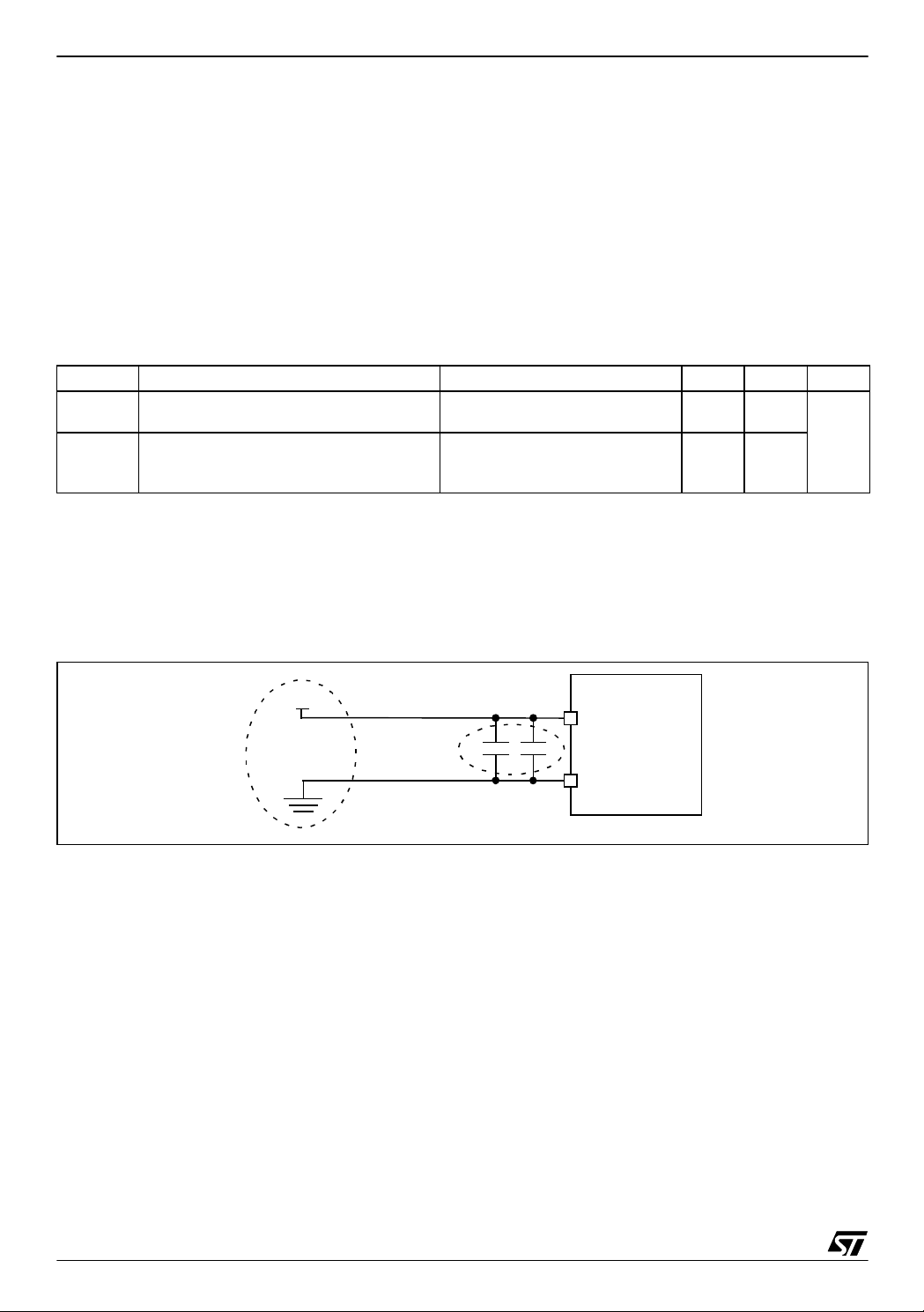
ST6215C/ST6225C
11.7 EMC CHARACTERISTICS
Susceptibility tests are performed on a sample basis during product characterization.
11.7.1 Functional EMS
(Electro Magnetic Susceptibility)
Based on a simple running application on the
product (toggling 2 LEDs through I/O ports), the
product is stressed by two electro magnetic events
until a failure occurs (indicated by the LEDs).
■ ESD: Electro-Static Discharge (positive and
negative) is applied on all pins of the device until
a functional disturbance occurs. This test
conforms with the IEC 1000-4-2 standard.
■ FTB: A Burst of Fast Transient voltage (positive
and negative) is applied to V
and VSS through
DD
a 100pF capacitor, until a functional disturbance
occurs. This test conforms with the IEC 1000-44 standard.
A device reset allows normal operations to be resumed.
Symbol Parameter Conditions Neg
V
V
FESD
FFTB
Voltage limits to be applied on any I/O pin
to induce a functional disturbance
Fast transient voltage burst limits to be applied through 100pF on V
DD
and V
DD
to induce a functional disturbance
VDD=5V, TA=+25°C, f
conforms to IEC 1000-4-2
=5V, TA=+25°C, f
V
pins
DD
conforms to IEC 1000-4-4
OSC
OSC
=8MHz
=8MHz
1)
-2 2
-2.5 3
Notes:
1. Data based on characterization results, not tested in production.
2. The suggested 10 µF and 0.1 µF decoupling capa citors on the power sup ply lines are propos ed as a good price vs.
EMC performance tradeoff. They have to be put as close as possible to the device power supply pins. Other EMC recommendations are given in other sections (I/Os, RESET, OSCx pin characteristics).
Figure 56. EMC Recommended Star Network Power Supply Connection
2)
Pos
1)
Unit
kV
POWER
SUPPLY
SOURCE
V
DD
ST6
DIGITAL NOISE
FILTERING
(close to the MCU)
0.1 µF10 µF
V
V
ST62XX
DD
SS
78/105
1
Page 79
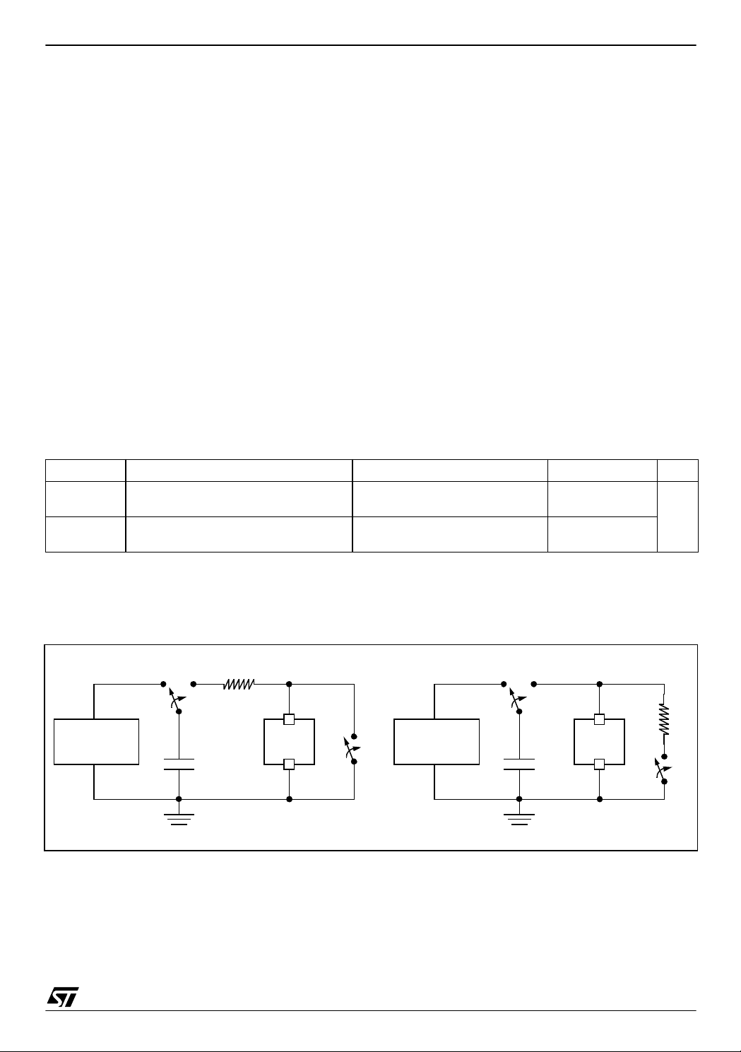
EMC CHARACTERISTICS (Cont’d)
11.7.2 Absolute Electrical Sensitivity
Based on three different tests (ESD, LU and DLU)
using specific measurement methods, the product
is stressed in order to determine its performance in
terms of electrical sensitivity. For more details, refer to the AN1181 application note.
11.7.2.1 Electro-Static Discharge (ESD)
Electro-Static Discharges (3 positive then 3 negative pulses separated by 1 second ) are applied to
the pins of each sample according to each pin
combination. The sample size depends of the
number of supply pins of the device (3 parts*(n+1)
supply pin). Two models are usually simulated:
Human Body Model and Machine Model. This test
conforms to the JESD 22-A114A/A1 15A standard.
See Figure 57 and the following test sequences.
Human Body Model Test Sequence
– C
is loaded through S1 by the HV pulse gener-
L
ator.
ST6215C/ST6225C
– S1 switches position from generator to R.
– A discharge from C
to the ST6 occurs.
– S2 must be closed 10 to 100ms after the pulse
delivery period to ensure the ST6 is not left in
charge state. S2 must be opened at least 10ms
prior to the delivery of the next pulse.
Machine Model Test Sequence
is loaded through S1 by the HV pulse gener-
– C
L
ator.
– S1 switches position from generator to ST6.
– A discharge from C
– S2 must be closed 10 to 100ms after the pulse
delivery period to ensure the ST6 is not left in
charge state. S2 must be opened at least 10ms
prior to the delivery of the next pulse.
– R (machine resistance), in series with S2, en-
sures a slow discharge of the ST6.
through R (body resistance)
L
to the ST6 occurs.
L
Absolute Maximum Ratings
Symbol Ratings Conditions Maximum value 1)Unit
V
ESD(HBM)
V
ESD(MM)
Notes:
1. Data based on characterization results, not tested in production.
Electro-static discharge voltage
(Human Body Model)
Electro-static discharge voltage
(Machine Model)
T
=+25°C
A
T
=+25°C
A
2000
200
Figure 57. Typical Equivalent ESD Circuits
HIGH VOLTAGE
PULSE
GENERATOR
S1
R=1500Ω
CL=100pF
HUMAN BODY MODEL MACHINE MODEL
ST6
HIGH VOLTAGE
S2
PULSE
GENERATOR
S1
ST6
CL=200pF
V
R=10k~10MΩ
S2
79/105
1
Page 80

ST6215C/ST6225C
EMC CHARACTERISTICS (Cont’d)
11.7.2.2 Static and Dynamic Latch-Up
■ LU: 3 complementary static tests are required
on 10 parts to assess the latch-up performance.
A supply overvoltage (applied to each power
supply pin), a current inje ction (applied to e ach
input, output and configurable I/O pin) and a
power supply switch sequence are performed
on each sample. This test conforms to the EIA/
JESD 78 IC latch-up standard. For more details,
refer to the AN1181 application note.
Electrical Sensitivities
Symbol Parameter Conditions Class
LU Static latch-up class
DLU Dynamic latch-up class
Notes:
1. Class description: A Class is an STMicroelectronics internal specification. All its limits are higher than the JEDEC specifications, that means when a device belongs to Class A it exceeds the JEDEC standard. B Class strictly covers all the
JEDEC criteria (international standard).
2. Schaffner NSG435 with a pointed test finger.
■ DLU: Electro-Static Discharges (one positive
then one negative test) are applied to each pin
of 3 samples when the micro is running to
assess the latch-up performance in dynamic
mode. Power supplies are set to the typical
values, the oscillator is connected as near as
possible to the pins of the micro and the
component is put in reset mode. This test
conforms to the IEC1000-4-2 and SAEJ1752/3
standards and is described in Figure 58. For
more details, refer to the AN1181 application
note.
=+25°C
T
A
T
=+85°C
A
V
DD
=5V, f
=4MHz, TA=+25°C
OSC
A
A
A
1)
Figure 58. Simplif ie d Diagram of the ESD Gen erat o r for D LU
ESD
GENERATOR
RCH=50MΩ RD=330Ω
CS=150pF
2)
HV RELAY
DISCHARGE
RETURNCONNECTION
DISCHARGE TIP
ST6
V
DD
V
SS
80/105
1
Page 81

EMC CHARACTERISTICS (Cont’d)
11.7.3 ESD Pin Protection Strategy
To protect an integrated circuit against ElectroStatic Discharge the stress must be c ontrolled to
prevent degradation or destruction of the circuit elements. The stress generally affects the circuit elements which are conn ected to the p ads but ca n
also affect the internal devices when the supply
pads receive the stress. The elements to be protected must n ot re ce i ve exce ssive current, vo lt a ge
or heating within their structure.
An ESD network combines the different input and
output ESD protections. This network works, by allowing safe discharge paths for the pins subjected
to ESD stress. Two critical ESD stress cases are
presented in F igure 59 and Figure 60 for standard
pins.
ST6215C/ST6225C
Standard Pin Protection
To protect the output structure the following elements are added:
– A diode to V
– A protection device between V
To protect the input structure the following ele-
ments are added:
– A resistor in series with the pad (1)
– A diode to V
– A protection device between V
(3a) and a diode from VSS (3b)
DD
and VSS (4)
DD
(2a) and a diode from VSS (2b)
DD
and VSS (4)
DD
Figure 59. Positive Stress on a Standard Pad vs. V
V
DD
(3a)
OUT
Mainpath
Path to avoid
V
SS
(3b)
Figure 60. Negative Stress on a Standard Pad vs. V
V
DD
(3a)
OUT
Mainpath
(3b)
SS
DD
(4)
(4)
V
DD
(2a)
IN
IN
(1)
(2b)
(2a)
(1)
(2b)
V
SS
V
DD
V
SS
V
SS
81/105
1
Page 82
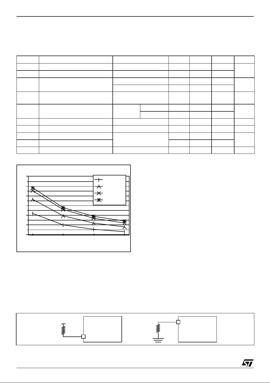
ST6215C/ST6225C
11.8 I/O PORT PIN CHARACTERISTICS
11.8.1 General Characteristics
Subject to general operating conditions for V
Symbol Parameter Conditions Min Typ
V
V
V
R
C
C
OUT
t
f(IO)out
t
r(IO)out
t
w(IT)in
Input low level voltage
IL
Input high level voltage
IH
Schmitt trigger voltage hysteresis
hys
I
Input leakage current
L
Weak pull-up equivalent resistor
PU
I/O input pin capacitance 5 10 pF
IN
I/O output pin capacitance 5 10 pF
Output high to low level fall time
Output low to high level rise time
External interrupt pulse time
Figure 61. Typical R
Rpu [Khom]
350
300
250
200
vs. VDD with V
PU
2)
2)
4)
5)
5)
6)
IN
Ta=-40°C
Ta=25°C
Ta=95°C
Ta=125°C
, f
DD
VDD=5V 200 400
3)
V
DD
V
SS≤VIN≤VDD
, and TA unless otherwise specified.
OSC
0.7xV
DD
=3.3V 200 400
(no pull-up configured)
V
IN=VSS
VDD=5V 40 110 350
=3.3V 80 230 700
V
DD
CL=50pF
Between 10% and 90%
1t
= V
SS
1)
Max Unit
0.3xV
DD
mV
0.1 1 µA
kΩ
30
35
ns
CPU
V
150
100
50
3456
VDD [V]
Notes:
1. Unless otherwise specified, typical data are based on T
=25°C and VDD=5V.
A
2. Data based on characterization results, not tested in production.
3. Hysteresis voltage between Schmitt trigger switching levels. Based on characterization results, not tested.
4. The R
not tested in production.
pull-up equivalent resis tor is based on a resistive transis tor. This data is based on charac terization resu lts,
PU
5. Data based on characterization results, not tested in production.
6. To generate an external interrupt, a minimum pulse width has to be applied on an I/O port pin configured as an external
interrupt source.
Figure 62. Two typical Applications with unused I/O Pin
V
DD
10kΩ
ST62XX
UNUSED I/O PORT
10kΩ
UNUSED I/OPO RT
ST62XX
82/105
1
Page 83

ST6215C/ST6225C
I/O PORT PIN CHARACTERISTICS (Cont’d)
11.8.2 Output Driving Current
Subject to general operating conditions for V
Symbol Parameter Condition s Min M ax Unit
Output low level voltage for a standard I/O pin
(see Figure 63 and Figure 66)
1)
V
OL
Output low level voltage for a high sink I/O pin
(see Figure 64 and Figure 67)
Output high level voltage for an I/O pin
2)
V
OH
Notes:
1. The I
(I/O ports and control pins) must not exceed I
2. The I
I
IO
(see Figure 65 and Figure 68)
current sunk must always respect the absolute maximum rating specified in Section 11.2.2 and the sum of I
IO
current source mus t alwa ys res pect the a bsolu te ma ximum rati ng specifie d in S ectio n 11.2 .2 an d the sum of
IO
(I/O ports and control pins) must not exceed I
, f
, and TA unless otherwise specified.
OSC
IIO=+10µA, T
I
=+3mA, T
IO
I
=+5mA, T
IO
I
=+10mA, T
IO
I
=+10µA, T
IO
I
=+7mA, T
IO
=5V
I
=+10mA, T
IO
DD
I
V
=+15mA, T
IO
I
=+20mA, T
IO
I
=+30mA, T
IO
I
=-10µA, T
IO
I
=-3mA, T
IO
I
=-5mA, T
IO
≤125°C 0.1
A
≤125°C 0.8
A
≤85°C 0.8
A
≤85°C 1.2
A
≤125°C 0.1
A
≤125°C 0.8
A
≤85°C 0.8
A
≤125°C 1.3
A
≤85°C 1.3
A
≤85°C 2
A
≤125°C V
A
≤125°C V
A
≤85°C V
A
. True open drain I/O pins does not have VOH.
VSS
DD
.
VDD
DD
DD
DD
-0.1
-1.5
-1.5
V
IO
Figure 63. Typical VOL at V
Vol [mV] at Vdd=5V
1000
800
600
400
200
Ta=-40°C
Ta=25°C
0
0246810
Ta=95°C
Ta=125°C
Iio [mA]
= 5V (standard) Figure 64. Typical VOL at V
DD
Vol [V] at Vdd=5V
1
Ta=-40°C
Ta=95°C
0.8
Ta=25°C
Ta=125°C
0.6
0.4
0.2
0
048121620
Iio [mA]
= 5V (high-sink)
DD
83/105
1
Page 84

ST6215C/ST6225C
I/O PORT PIN CHARACTERISTICS (Cont’d)
Figure 65. Typical V
Figure 66. Typical V
Vol [mV] at Iio=2mA
350
300
at V
OH
vs VDD (standard I/Os)
OL
= 5V
DD
Voh [V] at Vdd=5V
5
4.5
4
3.5
-8 -6 -4 -2 0
Ta=-40°C
Ta=25°C
Ta=95°C
Ta=125°C
Ta=-40°C
Ta=25°C
Iio [mA]
Vol [mV] at Iio=5mA
700
600
Ta=95°C
Ta=125°C
Ta=-40°C
Ta=25°C
Ta=95°C
Ta=125°C
250
200
150
3456
Figure 67. Typical V
Vol [V] at Iio=8mA
0.55
0.5
0.45
0.4
0.35
0.3
0.25
0.2
3456
VDD [V]
vs VDD (high-sink I/Os)
OL
Ta=-40°C
Ta=25°C
VDD [V]
Ta=95°C
Ta=125°C
500
400
300
3456
VDD [V]
Vol [V] at Iio=20mA
1.8
1.6
1.4
1.2
1
0.8
0.6
0.4
3456
VDD [V]
Ta=-40°C
Ta=25°C
Ta=95°C
Ta=125°C
84/105
1
Page 85

I/O PORT PIN CHARACTERISTICS (Cont’d)
ST6215C/ST6225C
Figure 68. Typical V
Voh [V] at Iio=-2mA
6
5
4
3
2
3456
OH
vs V
VDD [V]
DD
Ta=-40°C
Ta=25°C
Ta=95°C
Ta=125°C
Voh [V] at Iio=-5mA
6
5
4
3
2
1
3456
Ta=-40°C
Ta=25°C
VDD [V]
Ta=95°C
Ta=125°C
85/105
1
Page 86

ST6215C/ST6225C
11.9 CONTROL PIN CHARACTERISTICS
11.9.1 Asynchronous RESET
Subject to general operating conditions for V
Symbol Parameter Conditions Min Typ
V
V
V
R
R
t
w(RSTL)out
t
h(RSTL)in
t
g(RSTL)in
Input low level voltage
IL
Input high level voltage
IH
Schmitt trigger voltage hysteresis
hys
Weak pull-up equivalent resistor
ON
ESD resistor protection V
ESD
Generated reset pulse duration
External reset pulse hold time
Filtered glitch duration
Pin
2)
2)
6)
, f
DD
3)
4)
V
External pin or
internal reset sources
5)
, and TA unless otherwise specified.
OSC
0.7xV
DD
200 400 mV
VDD=5V 150 350 900
IN=VSS
=3.3V 300 730 1900
V
DD
VDD=5V 2.8
IN=VSS
=3.3V
V
DD
1)
Max Unit
0.3xV
DD
kΩ
kΩ
t
CPU
µs
µs
V
ns
Notes:
1. Unless otherwise specified, typical data are based on T
=25°C and VDD=5V.
A
2. Data based on characterization results, not tested in production.
3. Hysteresis voltage between Schmitt trigger switching levels. Based on characterization results, not tested.
4. The R
not tested in production.
5. All short pulse applied on RESET
pull-up equ ivalen t res istor is ba sed on a resi stive trans istor. This data is b ased on chara cteriz ation resu lts,
ON
pin with a duration below t
h(RSTL)in
can be ignored.
6. The reset network protects the device against parasitic resets, especially in a noisy environment.
7. The output of the external reset circuit must have an open-drain output to drive the ST6 reset pad. Otherwise the device
can be damaged when the ST6 generates an internal reset (LVD or watchdog).
Figure 69. Typical RON vs VDD with VIN=V
Ron [Kohm]
1000
900
800
700
600
500
400
300
200
100
3456
SS
Ta=-40°C
Ta=25°C
VDD [V]
Ta=95°C
Ta=125°C
86/105
1
Page 87

CONTROL PIN CHARACTERISTICS (Cont’d)
Figure 70. Typical Applic a t ion with RESET
pin
ST6215C/ST6225C
8)
OPTIONAL
EXTERNAL
RESET
CIRCUIT
V
DD
7)
0.1µF
0.1µF
V
DD
4.7kΩ
RESET
V
DD
R
PU
1)
R
ESD
f
INT
STOP MO DE
COUNTER
2048 external clock cycles
WATCHDOG RESET
LVD RESET
11.9.2 NMI Pin
, f
Subject to general operating conditions for V
DD
Symbol Parameter Conditions Min Typ
2)
2)
3)
4)
V
V
R
pull-up
V
V
Input low level voltage
IL
Input high level voltage
IH
Schmitt trigger voltage hysteresis
hys
Weak pull-up equivalent resistor
Notes:
1. Unless otherwise specified, typical data are based on T
2. Data based on characterization results, not tested in production.
3. Hysteresis voltage between Schmitt trigger switching levels. Based on characterization results, not tested.
4. The R
tested in production.
equivalent resistor is b ased on a resistive tra nsistor. Th is data is ba sed on cha racterizatio n results, n ot
pull-up
, and TA unless otherwise specified.
OSC
0.7xV
DD
200 400 mV
VDD=5V 40 100 350
IN=VSS
=25°C and VDD=5V.
A
=3.3V 80 200 700
V
DD
1)
Max Unit
0.3xV
DD
INTERNAL
RESET
kΩ
V
Figure 71. Typical R
vs. VDD with VIN=V
pull-up
Rpull-up [Kohm]
300
250
200
150
100
50
SS
Ta=-40°C
Ta=25°C
Ta=95°C
Ta=125°C
3456
VDD [V]
87/105
1
Page 88

ST6215C/ST6225C
CONTROL PIN CHARACTERISTICS (Cont’d)
11.10 TIMER PERIPHERAL CHARACTERISTICS
Subject to general operating conditions for V
f
, and TA unless otherwise specified.
OSC
DD
,
Refer to I/O port characteristics for more details on
the input/output alternate function characteristics
(TIMER).
11.10.1 Wa tc hdog Timer
Symbol Parameter Conditions Min Typ Max Unit
3,072 196,608 t
t
w(WDG)
Watchdog time-out duration
f
=4MHz 0.768 49.152 ms
CPU
f
=8MHz 0.384 24.576 ms
CPU
11.10.2 8-Bit Timer
Symbol Parameter Conditions Min Typ Max Unit
f
EXT
Timer external clock frequency 0 f
t
Pulse width at TIMER pin
w
VDD>4.5V 125 ns
VDD=3V 1 µs
/4 MHz
INT
INT
88/105
1
Page 89

11.11 8-BIT ADC CHARACTERISTICS
ST6215C/ST6225C
Subject to general operating conditions for V
Symbol Parameter Conditions Min Typ
f
OSC
V
R
t
ADC
t
STAB
AD
AC
Clock frequency 1.2 f
Conversion range voltage
AIN
External input resistor 10
AIN
2)
Total convertion time
Stabilization time
Analog input current during conver-
I
sion
Analog input capacitance 2 5 pF
IN
4)
, f
, and TA unless otherwise specified.
OSC
V
SS
=8MHz
=4MHz
70
140
1)
Max Unit
OSC
V
DD
3)
f
OSC
f
OSC
DD
24t
f
=8MHz 3.25 6.5 µs
OSC
1.0 µA
MHz
V
kΩ
µs
CPU
Notes:
1. Unless otherwise specified, typical data are based on T
2. The ADC refers to V
and VSS.
DD
=25°C and VDD=5V.
A
3. Any added external serial resistor will downgrade the ADC accuracy (especially for resistance greater than 10kΩ). Data
based on characterization results, not tested in production.
4. As a stabilization time for the AD converter is required, the first conversion after the enable can be wrong.
Figure 72. Typical Application with ADC
R
V
AIN
AIN
AINx
r≈150Ω
10pF
ADC
10MΩ
Note: ADC not present on some devices. See device summary on page 1.
ST62XX
89/105
1
Page 90
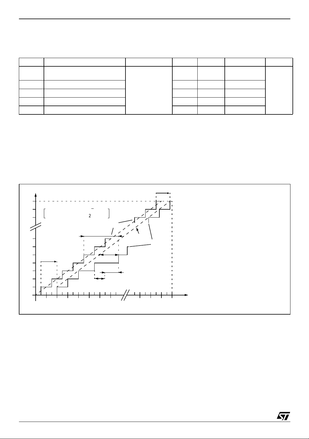
ST6215C/ST6225C
8-BIT ADC CHARACTERISTICS (Cont’d)
ADC Accuracy
Symbol Parameter Conditions Min Typ. Max Unit
| Total unadjusted error
|E
T
E
E
|E
|E
Offset error
O
Gain Error
G
| Differential linearity error
D
| Integral linearity error
L
1)
1)
1)
1)
1)
VDD=5V
f
=8MHz
OSC
2)
1.2
0.72
-0.31
0.54
Notes:
1. Negative injection disturbs the analog performance of the device. In particular, it induces leakage currents throughout
the device including the analog inputs. To avoid undesirable effects on the analog functions, care must be taken:
- Analog input pins must have a negative injection less than 1mA (assuming that the impedance of the analog voltage
is lower than the specified limits).
- Pure digital pins must have a negative injection less than 1mA. In addition, it is recommended to inject the current as
far as possible from the analog input pins.
2. Data based on characterization results over the whole temperature range, monitored in production.
Figure 73. ADC Accuracy Characteristics
±2, fosc>1.2MHz
±4, fosc>32KHz
LSB
Digit al Result AD CDR
255
254
253
1LSB
7
6
5
4
3
2
1
E
0
1234567
V
SSA
O
IDEAL
V
–
DDAVSSA
---------------------------------------- -=
256
E
1LSB
T
IDEAL
(2)
(3)
E
L
E
D
253 254 255 256
(1)
E
G
V
DDA
Note: ADC not present on some devices. See device summary on page 1.
(1) Example of an actual transfer curve
(2) The ideal transfer curve
(3) End poi n t correlation l i ne
=Total Unadjusted Error: maximum deviation
E
T
between the actual and th e i deal transfer c urves.
=Offset Er ror: deviation between the firs t ac tual
E
O
transition and the first ideal one.
=Gain E rror: deviation between the last ideal
E
G
transition and the last actual one.
=Differential Linearity Error: maximum deviation
E
D
between actual steps a nd t he i deal one.
=Integral Linearity Error: maximum deviation
E
L
between an y actual transit ion and the e nd point
correlation line.
Vin (LSB
IDEAL
)
90/105
1
Page 91

12 GENERAL INFORMATION
12.1 PACKAGE MECHANICAL DATA Figure 74. 28-Pin Plastic Dual In-Line Package, 600-mil Width
ST6215C/ST6225C
E
AA2
A1
D1
L
C
BB1
D
e
E1
eB
Figure 75. 28-Pin Plastic Small Outline Package, 300-mil Width
D
L
L
A
A1
e
B
a
HE
h x 45×
Dim.
mm inches
Min Typ Max Min Typ Max
A 6.35 0.250
A1 0.38 0.015
A2 3.18 4.95 0.125 0.195
B 0.36 0.56 0.014 0.022
B1 0.76 1.78 0.030 0.070
C 0.20 0.38 0.008 0.015
D 35.05 39.75 1.380 1.565
D1 0.13 0.005
e 2.54 0.100
eB 17.78 0.700
E 15.24 15.88 0.600 0.625
E1 12.32 14.73 0.485 0.580
L 2.92 5.08 0.115 0.200
Number of Pins
N 28
Dim.
mm inches
Min Typ Max Min Typ Max
A 2.35 2.65 0.093 0.104
A1 0.10 0.30 0.004 0.012
C
B 0.33 0.51 0.013 0.020
C 0.23 0.32 0.009 0.013
D 17.70 18.10 0.697 0.713
E 7.40 7.60 0.291 0.299
e 1.27 0.050
H 10.00 10.65 0.394 0.419
h 0.25 0.75 0.010 0.030
α 0° 8° 0° 8°
L 0.40 1.27 0.016 0.050
Number of Pins
N 28
91/105
1
Page 92
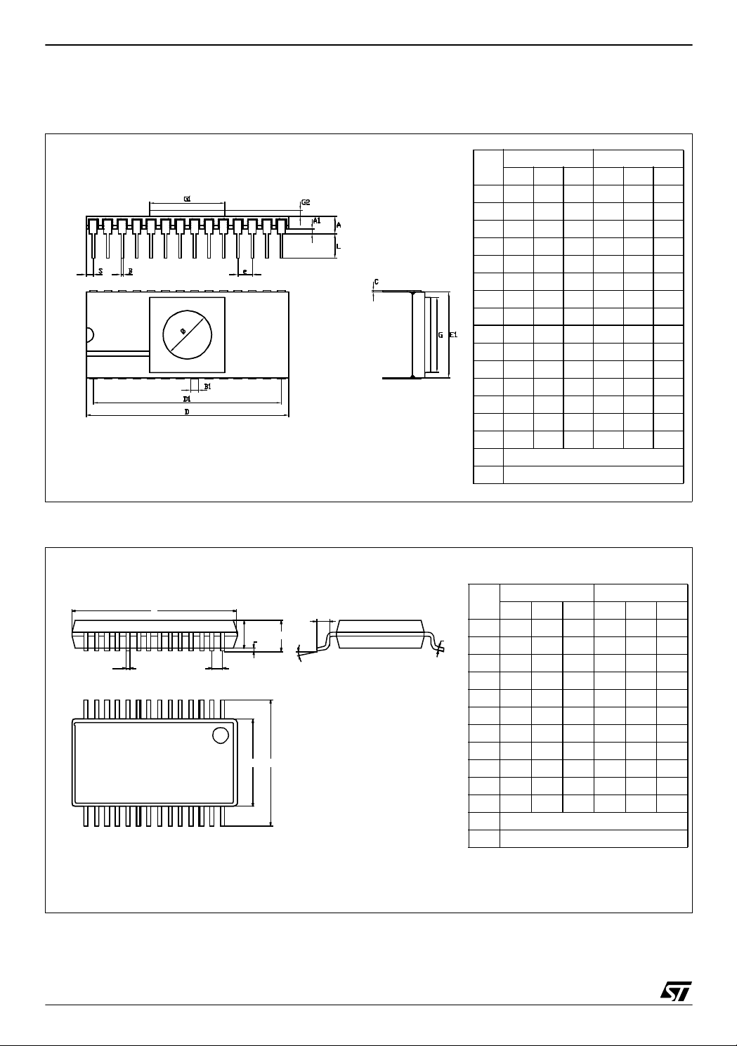
ST6215C/ST6225C
PACKAGE MECHANICAL DATA (Cont’d)
Figure 76. 28-Pin Ceramic Side-Brazed Dual In-Line Package
CDIP28W
Figure 77. 28-Pin Plastic Shrink Small Outline Package
Dim.
mm inches
Min Typ Max Min Typ Max
A 4.17 0.164
A1 0.76 0.030
B 0.36 0.46 0.56 0.014 0.018 0.022
B1 0.76 1.27 1.78 0.030 0.050 0.070
C 0.20 0.25 0.38 0.008 0.010 0.015
D 34.95 35.56 36.17 1.376 1.400 1.424
D1 33.02 1.300
E1 14.61 15.11 15.62 0.575 0.595 0.615
e 2.54 0.100
G 12.70 12.95 13.21 0.500 0.510 0.520
G1 12.70 12.95 13.21 0.500 0.510 0.520
G2 1.14 0.045
L 2.92 5.08 0.115 0.200
S 1.27 0.050
Ø 8.89 0.350
Number of Pins
N28
92/105
D
A2
A
A1
b
e
L
h
Dim.
A 2.00 0.079
c
A1 0.05 0.002
A2 1.65 1.75 1.85 0.065 0.069 0.073
b 0.22 0.38 0.009 0.015
mm inches
Min Typ Max Min Typ Max
c 0.09 0.25 0.004 0.010
D 9.90 10.20 10.50 0.390 0.402 0.413
E 7.40 7.80 8.20 0.291 0.307 0.323
E1 E
E1 5.00 5.30 5.60 0.197 0.209 0.220
e 0.65 0.026
θ 0° 4° 8° 0° 4° 8°
L 0.55 0.75 0.95 0.022 0.030 0.037
Number of Pins
N 28
1
Page 93

12.2 THERMAL CHARACTERISTICS
Symbol Ratings Value Unit
Package thermal resistance (junction to ambient)
R
thJA
P
D
T
Jmax
Notes:
1. The power dissipation is obtained from the formula P
and P
is the port power dissipation determined by the user.
PORT
2. The average chip-junction temperature can be obtained from the formula T
DIP28
SO28
SSOP28
Power dissipation
1)
Maximum junction temperature
D
2)
= P
INT
+ P
PORT
where P
ST6215C/ST6225C
55
75
110
500 mW
150 °C
is the chip internal power (IDDxVDD)
INT
= TA + PD x RthJA.
J
°C/W
93/105
1
Page 94

ST6215C/ST6225C
12.3 SOLDERING AND GLUEABILITY INFORMATION
Recommended soldering information given only
as design guidelines in Figure 78 and Figure 79.
Recommended glue for SMD plastic packages:
■ Heraeus: PD945, PD955
■ Loctite: 3615, 3298
Figure 78. Recommended Wave So ldering Profi le (with 37% Sn and 63% Pb)
Temp. [°C]
250
200
150
100
50
0
80°C
PREHEATING
PHASE
20 60
5 sec
SOLDERING
PHASE
40 80
COOLING PHASE
(ROOM T EMPE RAT URE)
100 140
120 160
Figure 79. Recommended Re fl ow Soldering Ove n Profile (MID JED EC)
Temp. [°C]
250
200
150
100
50
90 sec at 125°C
ramp up
2°C/sec for 50sec
150 sec above 183°C
Tmax=220+/-5°C
for 25 sec
ramp down natural
2°C/sec max
Time [sec]
94/105
0
100 200
300 400
Time [sec]
1
Page 95

12.4 PACKAGE/SOCKET FOOTPRINT PROPOSAL
Table 22. Suggested List of DIP28 Socket Types
ST6215C/ST6225C
Package / Probe Adaptor / Socket Reference
DIP28 TEXTOOL 22 8-60-2 3 X Textool
Same
Footprint
Socket Type
Table 23. Suggested List of SO28 Socket Typ es
Package / Probe Adaptor / Socket Reference
SO28
EMU PROBE
Programming
Adapter
ENPLAS OTS-28-1.27-04 Open Top
YAMAICHI IC51-0282-334-1 Clamshell
Adapter from SO28 to DIP28 footprint
(delivered with emulator)
Logical Systems PA28SO1-08-6 X Open Top
Same
Footprint
X SMD to DIP
Socket Type
Table 24. Suggested List of SSOP28 Socket Types
Package / Probe Adaptor / Socket Reference
SSOP28 ENPLAS OTS-28-0.65-01 Open Top
EMU PROBE
Programming
Adapter
Adapter from SSOP28 to DIP28 footprint
(sales type: ST626X-P /SSO P28)
Logical Systems PA28SS-OT-6 X Open Top
Same
Footprint
X DIP to SMD
Socket Type
95/105
1
Page 96
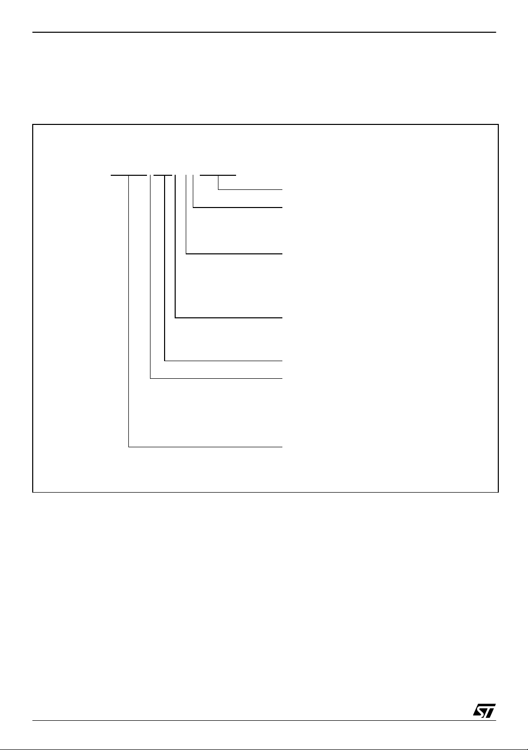
ST6215C/ST6225C
12.5 ORDERING INFORMATION
The following section deals with the procedure for
transfer of customer codes to STMicroelect ronics
Figure 80. ST6 Factory Coded D evice Types
ST62T25CB6/CCC
and also details the ST6 factory coded device
type.
ROM code
Temperature code:
1: Standard 0 to +70 °C
3: Automotive -40 to +125 °C
6: Industrial -40 to +85 °C
Package type:
B: Plastic DIP
D: Ceramic DIP
M: Plastic SOP
N: Plastic SSOP
T: Plastic TQFP
Revision index:
B,C: Product Definition change
L: Low Voltage Device
ST6 Sub family
Version Code:
No char: ROM
E: EPROM
P: FASTROM
T: OTP
Family
96/105
1
Page 97

12.6 TRANSFER OF CUSTOMER CODE
ST6215C/ST6225C
Customer code is made up of the RO M contents
and the list of the selected FASTROM options.
The ROM contents are to be sent on diskette, or
by electronic means, with the hexadecimal file
generated by the development tool. All unused
bytes must be set to FFh.
The selected options are communicated to
STMicroelectronics using the correctly filled OPTION LIST appended.
The STMicroelectronics Sales Organization will be
pleased to provide detailed information on contractual points.
Listing Generation and Verification. When
STMicroelectronics receives the user’s ROM contents, a computer listing is generated from it. This
listing refers exactly to the ROM contents and options which will be used t o produce the specified
MCU. The listing is then returned to the custom er
who must thoroughly check, complete, sign and
return it to STMicroelectronics. The signed listing
forms a part of the contractual agreement for the
production of the specific customer MCU.
12.6.1 FASTROM Version
The ST62P15C/P25C are the Factory Advan ced
Service Technique ROM (FASTROM) versions of
ST62T15C,T25C OTP devices.
They offer the same functionality as OTP devices,
but they do not have to be programmed by the
customer. The customer code must be sent to
STMicroelectronics in the same way as for ROM
devices. The FASTR OM option list has the same
options as defined in the programmable option
byte of the OTP version . It also of fers an identifier
option. If this option is enabled, each FASTROM
device is programmed with a unique 5-byte
number which is mapped at addresses 0F9Bh0F9Fh. The user must therefore leave these bytes
blanked.
The identification number is structured as follows:
0F9Bh T0
0F9Ch T1
0F9Dh T2
0F9Eh T3
0F9Fh Test ID
with T0, T1, T2, T3 = time in seconds since 01/01/
1970 and Test ID = Tester Identifier.
97/105
1
Page 98

ST6215C/ST6225C
TRANSFER OF CUSTOMER CODE (Cont’d)
12.6.2 ROM Version
The ST6215C/25C are mask programmed ROM
version of ST62T15C,T25C OTP devices.
They offer the same functionality as OTP devices,
selecting as ROM options the options def ined in
the programmable option byte of the OTP version.
Figure 81. Programming Circuit
5V
V
DD
V
SS
4.7µF
100nF
ROM Readout Protection. If th e ROM READOUT
PROTECTION option is selected, a protection
fuse can be blown to prevent any access to the
program memory content.
In case the user wants to blow this fuse, high voltage must be applied on the V
PP
pin.
Figure 82. Programm ing wave form
V
PP
15
14V typ
10
100 µs max
5
0.5s min
PROTECT
V
PP
100nF
Note: ZPD15 is used for overvoltage protection
ZPD15
15V
VR02003
V
PP
14V
400mA
max
4mA typ
150 µs typ
t
VR02001
98/105
1
Page 99

ST6215C/ST6225C
ST6215C/25C/P15C/P25C MICROCONTROLLER OPTION LIST
Customer: . . . . . . . . . . . . . . . . . . . . . . . . . . . . . . . . . . . . . . . . . . . . . . . . . . . . . . . . . . . . . . . . . . . . . . . . . .
Address: . . . . . . . . . . . . . . . . . . . . . . . . . . . . . . . . . . . . . . . . . . . . . . . . . . . . . . . . . . . . . . . . . . . . . . . . . .
. . . . . . . . . . . . . . . . . . . . . . . . . . . . . . . . . . . . . . . . . . . . . . . . . . . . . . . . . . . . . . . . . . . . . . . . . .
Contact: . . . . . . . . . . . . . . . . . . . . . . . . . . . . . . . . . . . . . . . . . . . . . . . . . . . . . . . . . . . . . . . . . . . . . . . . . .
Phone: . . . . . . . . . . . . . . . . . . . . . . . . . . . . . . . . . . . . . . . . . . . . . . . . . . . . . . . . . . . . . . . . . . . . . . . . . .
Reference: . . . . . . . . . . . . . . . . . . . . . . . . . . . . . . . . . . . . . . . . . . . . . . . . . . . . . . . . . . . . . . . . . . . . . . . . . .
STMicroelectronics references:
Device: [ ] ST6215C (2 KB) [ ] ST6225C (4 KB)
Package: [ ] Dual in Line Plastic
Conditioning option: [ ] Standard (Tube) [ ] Tape & Reel
Temperature Range: [ ] 0°C to + 70°C [ ] - 40°C to + 85°C
Marking: [ ] Standard marking
[ ] Special marking (ROM only):
PDIP28 (10 char. max): _ _ _ _ _ _ _ _ _ _
PSO28 (8 char. max): _ _ _ _ _ _ _ _
Authorized characters are letters, digits, '.', '-', '/' and spaces only.
Oscillator Safeguard: [ ] Enabled [ ] Disabled
Watchdog Selection: [ ] Software Activation [ ] Hardware Activation
Timer pull-up: [ ] Enabled [ ] Disabled
NMI pull-up: [ ] Enabled [ ] Disabled
Oscillator Selection: [ ] Quartz crystal / Ceramic resonator
Readout Protection: FASTROM:
ROM:
[ ] Fuse is blown by STMicroelectronics
[ ] Fuse can be blown by the customer
[ ] ST62P15C (2 KB) [ ] ST62P25C (4 KB)
[ ] Small Outline Plastic with conditioning
[ ] Shrink Small Outline Plastic with conditioning
[ ] - 40°C to + 125°C
SSOP28 (11 char. max): _ _ _ _ _ _ _ _ _ _ _
[ ] RC network
[ ] Enabled [ ] Disabled
[ ] Enabled:
[ ] Disabled
Low Voltage Detector: [ ] Enabled [ ] Disabled
External STOP Mode Control: [ ] Enabled [ ] Disabled
Identifier (FASTROM only): [ ] Enabled [ ] Disabled
Comments:
Oscillator Frequency in the application: . . . . . . . . . . . . . . . . . . . . . . . . . . . . . . . . . . . . . . . . . . . . . .
Supply Operating Range in the application: . . . . . . . . . . . . . . . . . . . . . . . . . . . . . . . . . . . . . . . . . . . . . .
Notes: . . . . . . . . . . . . . . . . . . . . . . . . . . . . . . . . . . . . . . . . . . . . . . . . . . . . . . . . . . . . . . . . . . . . . . . . . .
Date: . . . . . . . . . . . . . . . . . . . . . . . . . . . . . . . . . . . . . . . . . . . . . . . . . . . . . . . . . . . . . . . . . . . . . . . . . .
Signature: . . . . . . . . . . . . . . . . . . . . . . . . . . . . . . . . . . . . . . . . . . . . . . . . . . . . . . . . . . . . . . . . . . . . . . . . . .
99/105
1
Page 100

ST6215C/ST6225C
13 DEVELOPMENT TOOLS
STMicroelectronics offers a range of hardware
and software development tools for the ST6 micro-
tain from the STMicroelectronics Internet site:
➟ ht tp://mc u.st.com.
controller family. Full details of tools available for
the ST6 from third party manufacturers can be ob-
Table 25. Dedicated Third Parties Development Tools
Third Party
ACTUM
CEIBO
RAISONANCE
SOFTEC
ADVANCED EQUIPMENT
ADVANCED TRANSDATA
BP MICROSYSTEMS
DATA I/O http://www.data-io.com/
DATAMAN http://www.dataman.com/
EE TOOLS
ELNEC http://www.elnec.com/
HI-LO SYSTEMS http://www.hilosystems.com.tw/
ICE TECHNOLOGY
LEAP http://www.leap.com.tw/
LLOYD RESEARCH http://www.lloyd-research.com/
LOGICAL DEVICES
MQP ELECTRONICS http://www.mqp.com/
NEEDHAMS
ELECTRONIC S
STAG PROGRAMMERS
SYSTEM GENERAL CORP http://www.sg.com.tw
TRIBAL MICROSYSTEMS http://www.tribalmicro.com/
XELTEK
1)
ST-REALIZER II: Graphical Schematic
based Development available from
STMicroelectronics.
Low cost emulator available from CEIBO.
This tool includes in the same environment: an assembler, linker, C compiler,
debugger and simulator. The assembler
package (plus limited C compiler) is free
and can be downloaded from raisonance
web site. The full version is available
both from STMicroelectronics and Raisonance.
High end emulator available from
SOFTEC.
Gang programmer available from
SOFTEC.
Single and gang programmers
Designation ST Sales Type Web site address
STREALIZER-II
ST6RAIS-SWC/
PC
http://www.actum.com/
http://www.ceibo.com/
http://www.raisonance.com/
http://www.softecmicro.com/
http://www.aec.com.tw/
http://www.adv-transdata.com/
http://www.bpmicro.com/
http://www.eetools.com/
http://www.icetech.com/
http://www.chipprogram-
mers.com /
http://ww w .n eedh a m s. co m /
http://www.stag.co.uk/
http://www.xeltek.com/
Note 1: For latest information on third party tools, please visit our Internet site: ➟ http://mcu.st.com.
100/105
1
 Loading...