

STMicroelectronics ST6208C, ST6209C, ST6210C, ST6220C Technical data
ST6208C/ST6209C
ST6210C/ST6220C
8-BIT MCUs WITH A/D CONVERTER,
TWO TIMERS, OSCILLATOR SAFEGUARD & SAFE RESET
■ Memories
– 1K, 2K or 4K bytes Program memory (OT P,
EPROM, FASTROM or ROM) with read-out
protection
– 64 bytes RAM
■ Clock, Re set and Supply M a nagement
– Enhanced reset system
– Low Voltage Detector (LVD) for Safe Reset
– Clock sources: crystal/ceramic resonator or
RC netwo rk, ex tern al cloc k, bac kup o scillat or
(LFAO)
– Oscillator Safeguard (OSG)
– 2 Power Saving Modes: Wait and Stop
■ Interrupt Management
– 4 interrupt vectors plus NMI and RESET
– 12 external interrupt lines (on 2 vectors)
■ 12 I/ O P o rts
– 12 multifunctional bidirectional I/O lines
– 8 alternate function lines
– 4 high sink outputs (20mA)
■ 2 Timers
– Configurable watchdog timer
– 8-bit timer/counter with a 7-bit prescaler
■ Analog Peripheral
– 8-bit ADC with 4 or 8 input channels (except
on ST6208C)
(See Section 11.5 for Ordering Information)
■ Instruction Set
– 8-bit data manipulation
– 40 basic instructions
– 9 addressing modes
– Bit manipulation
■ Development Tools
– Full hardware/software development package
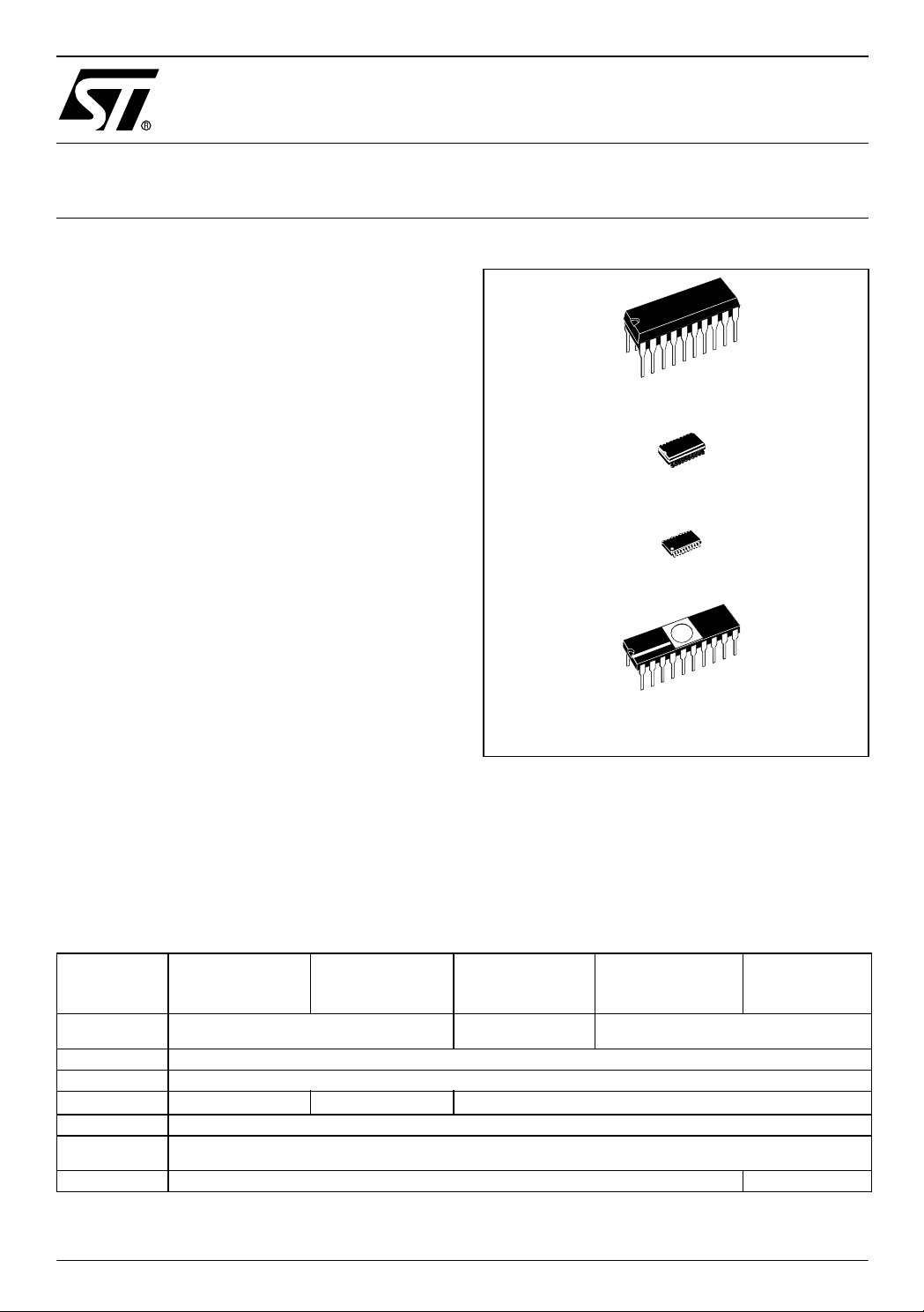
PDIP20
SO20
SSOP20
CDIP20W
Device Summary
Features
Program memory
- bytes
RAM - byte s 64
Operati ng Supply 3.0V to 6V
Analog Inputs Clock Fre quency 8M Hz Max
Operati ng
Temperature
Packages PDIP20/SO20/SSOP20 CDIP20W
ST62T08C(OTP)/
ST6208C(ROM)
ST62P08C(FASTROM)
ST62T09C(OTP)/
ST6209C (ROM)
ST62P09C(FASTROM)
1K 2K 4K
48
ST62T10C(OTP)/
ST6210C (ROM)
ST62P10C(FASTROM)
-40°C to +125°C
ST62T20C(OTP)
ST6220C(ROM)
ST62P20C(FASTROM)
ST62E20C(EPROM)
Rev. 3.3
October 2003 1/104
1

Table of Contents
1 INTRODUCTION . . . . . . . . . . . . . . . . . . . . . . . . . . . . . . . . . . . . . . . . . . . . . . . . . . . . . . . . . . . . . . 6
2 PIN DESCRIPTION . . . . . . . . . . . . . . . . . . . . . . . . . . . . . . . . . . . . . . . . . . . . . . . . . . . . . . . . . . . . 7
3 MEMORY MAPS, PROGRAMMING MODES AND OPTION BYTES . . . . . . . . . . . . . . . . . . . . . . 9
3.1 MEMORY AND REGISTER MAPS . . . . . . . . . . . . . . . . . . . . . . . . . . . . . . . . . . . . . . . . . . 9
3.1.1 Introduction . . . . . . . . . . . . . . . . . . . . . . . . . . . . . . . . . . . . . . . . . . . . . . . . . . . . . . . . 9
3.1.2 Program Space . . . . . . . . . . . . . . . . . . . . . . . . . . . . . . . . . . . . . . . . . . . . . . . . . . . . 11
3.1.3 Readout Protection . . . . . . . . . . . . . . . . . . . . . . . . . . . . . . . . . . . . . . . . . . . . . . . . . 11
3.1.4 Data Space . . . . . . . . . . . . . . . . . . . . . . . . . . . . . . . . . . . . . . . . . . . . . . . . . . . . . . . 11
3.1.5 Stack Space . . . . . . . . . . . . . . . . . . . . . . . . . . . . . . . . . . . . . . . . . . . . . . . . . . . . . . . 11
3.1.6 Data ROM Window . . . . . . . . . . . . . . . . . . . . . . . . . . . . . . . . . . . . . . . . . . . . . . . . . 13
3.2 PROGRAMMING MODES . . . . . . . . . . . . . . . . . . . . . . . . . . . . . . . . . . . . . . . . . . . . . . . . 15
3.2.1 Program Memory . . . . . . . . . . . . . . . . . . . . . . . . . . . . . . . . . . . . . . . . . . . . . . . . . . . 15
3.2.2 EPROM Erasing . . . . . . . . . . . . . . . . . . . . . . . . . . . . . . . . . . . . . . . . . . . . . . . . . . . . 15
3.3 OPTION BYTES . . . . . . . . . . . . . . . . . . . . . . . . . . . . . . . . . . . . . . . . . . . . . . . . . . . . . . . 16
4 CENTRAL PROCESSING UNIT . . . . . . . . . . . . . . . . . . . . . . . . . . . . . . . . . . . . . . . . . . . . . . . . . 17
4.1 INTRODUCTION . . . . . . . . . . . . . . . . . . . . . . . . . . . . . . . . . . . . . . . . . . . . . . . . . . . . . . . 17
4.2 MAIN FEATURES . . . . . . . . . . . . . . . . . . . . . . . . . . . . . . . . . . . . . . . . . . . . . . . . . . . . . . 17
4.3 CPU REGISTERS . . . . . . . . . . . . . . . . . . . . . . . . . . . . . . . . . . . . . . . . . . . . . . . . . . . . . . 17
5 CLOCKS, SUPPLY AND RESET . . . . . . . . . . . . . . . . . . . . . . . . . . . . . . . . . . . . . . . . . . . . . . . . 19
5.1 CLOCK SYSTEM . . . . . . . . . . . . . . . . . . . . . . . . . . . . . . . . . . . . . . . . . . . . . . . . . . . . . . . 19
5.1.1 Main Oscillator . . . . . . . . . . . . . . . . . . . . . . . . . . . . . . . . . . . . . . . . . . . . . . . . . . . . . 20
5.1.2 Oscillator Safeguard (OSG) . . . . . . . . . . . . . . . . . . . . . . . . . . . . . . . . . . . . . . . . . . . 21
5.1.3 Low Frequenc y Au xiliar y Os c illa tor ( LFA O) . . . . . . . . . . . . . . . . . . . . . . . . . . . . . . . 22
5.1.4 Register Description . . . . . . . . . . . . . . . . . . . . . . . . . . . . . . . . . . . . . . . . . . . . . . . . . 22
5.2 LOW VOLTAGE DETECTOR (LVD) . . . . . . . . . . . . . . . . . . . . . . . . . . . . . . . . . . . . . . . . 23
5.3 RESET . . . . . . . . . . . . . . . . . . . . . . . . . . . . . . . . . . . . . . . . . . . . . . . . . . . . . . . . . . . . . . . 24
5.3.1 Introduction . . . . . . . . . . . . . . . . . . . . . . . . . . . . . . . . . . . . . . . . . . . . . . . . . . . . . . . 24
5.3.2 RESET Sequence . . . . . . . . . . . . . . . . . . . . . . . . . . . . . . . . . . . . . . . . . . . . . . . . . . 24
5.3.3 RESET
5.3.4 Watchdog Reset . . . . . . . . . . . . . . . . . . . . . . . . . . . . . . . . . . . . . . . . . . . . . . . . . . . 26
5.3.5 LVD Reset . . . . . . . . . . . . . . . . . . . . . . . . . . . . . . . . . . . . . . . . . . . . . . . . . . . . . . . . 26
5.4 INTERRUPTS . . . . . . . . . . . . . . . . . . . . . . . . . . . . . . . . . . . . . . . . . . . . . . . . . . . . . . . . . 27
5.5 INTERRUPT RULES AND PRIORITY MANAGEMENT . . . . . . . . . . . . . . . . . . . . . . . . . 28
5.6 INTERRUPTS AND LOW POWER MODES . . . . . . . . . . . . . . . . . . . . . . . . . . . . . . . . . . 28
5.7 NON MASKABLE INTERRUPT . . . . . . . . . . . . . . . . . . . . . . . . . . . . . . . . . . . . . . . . . . . . 28
5.8 PERIPHERAL INTERRUPTS . . . . . . . . . . . . . . . . . . . . . . . . . . . . . . . . . . . . . . . . . . . . . 28
5.9 EXTERNAL INTERRUPTS (I/O PORTS) . . . . . . . . . . . . . . . . . . . . . . . . . . . . . . . . . . . . 29
5.9.1 Notes on using External Interrupts . . . . . . . . . . . . . . . . . . . . . . . . . . . . . . . . . . . . . . 29
5.10 INTERRUPT HANDLING PROCEDURE . . . . . . . . . . . . . . . . . . . . . . . . . . . . . . . . . . . . . 30
5.10.1Interrupt Response Time . . . . . . . . . . . . . . . . . . . . . . . . . . . . . . . . . . . . . . . . . . . . . 30
5.11 REGISTER DESCRIPTION . . . . . . . . . . . . . . . . . . . . . . . . . . . . . . . . . . . . . . . . . . . . . . . 31
6 POWER SAVING MODES . . . . . . . . . . . . . . . . . . . . . . . . . . . . . . . . . . . . . . . . . . . . . . . . . . . . . 32
6.1 INTRODUCTION . . . . . . . . . . . . . . . . . . . . . . . . . . . . . . . . . . . . . . . . . . . . . . . . . . . . . . . 32
Pin . . . . . . . . . . . . . . . . . . . . . . . . . . . . . . . . . . . . . . . . . . . . . . . . . . . . . . . . 25
104
2/104
2

Table of Contents
6.2 WAIT MODE . . . . . . . . . . . . . . . . . . . . . . . . . . . . . . . . . . . . . . . . . . . . . . . . . . . . . . . . . . 33
6.3 STOP MODE . . . . . . . . . . . . . . . . . . . . . . . . . . . . . . . . . . . . . . . . . . . . . . . . . . . . . . . . . . 34
6.4 NOTES RELATED TO WAIT AND STOP MODES . . . . . . . . . . . . . . . . . . . . . . . . . . . . . 36
6.4.1 Exit from Wait and Stop Modes . . . . . . . . . . . . . . . . . . . . . . . . . . . . . . . . . . . . . . . . 36
6.4.2 Recommende d MCU Configuration . . . . . . . . . . . . . . . . . . . . . . . . . . . . . . . . . . . . . 36
7 I/O PORTS . . . . . . . . . . . . . . . . . . . . . . . . . . . . . . . . . . . . . . . . . . . . . . . . . . . . . . . . . . . . . . . . . . 3 7
7.1 INTRODUCTION . . . . . . . . . . . . . . . . . . . . . . . . . . . . . . . . . . . . . . . . . . . . . . . . . . . . . . . 37
7.2 FUNCTIONAL DESCRIPTION . . . . . . . . . . . . . . . . . . . . . . . . . . . . . . . . . . . . . . . . . . . . 37
7.2.1 Digital Input Modes . . . . . . . . . . . . . . . . . . . . . . . . . . . . . . . . . . . . . . . . . . . . . . . . . 37
7.2.2 Analog Inputs . . . . . . . . . . . . . . . . . . . . . . . . . . . . . . . . . . . . . . . . . . . . . . . . . . . . . . 37
7.2.3 Output Modes . . . . . . . . . . . . . . . . . . . . . . . . . . . . . . . . . . . . . . . . . . . . . . . . . . . . . 37
7.2.4 Alternate Functions . . . . . . . . . . . . . . . . . . . . . . . . . . . . . . . . . . . . . . . . . . . . . . . . . 37
7.2.5 Instructions NOT to be used to access Port Data registers (SET, RES, INC and DEC) 39
7.2.6 Recommendations . . . . . . . . . . . . . . . . . . . . . . . . . . . . . . . . . . . . . . . . . . . . . . . . . . 39
7.3 LOW POWER MODES . . . . . . . . . . . . . . . . . . . . . . . . . . . . . . . . . . . . . . . . . . . . . . . . . . 39
7.4 INTERRUPTS . . . . . . . . . . . . . . . . . . . . . . . . . . . . . . . . . . . . . . . . . . . . . . . . . . . . . . . . . 39
7.5 REGISTER DESCRIPTION . . . . . . . . . . . . . . . . . . . . . . . . . . . . . . . . . . . . . . . . . . . . . . . 41
8 ON-CHIP PERIPHERALS . . . . . . . . . . . . . . . . . . . . . . . . . . . . . . . . . . . . . . . . . . . . . . . . . . . . . . 42
8.1 WATCHDOG TIMER (WDG) . . . . . . . . . . . . . . . . . . . . . . . . . . . . . . . . . . . . . . . . . . . . . . 42
8.1.1 Introduction . . . . . . . . . . . . . . . . . . . . . . . . . . . . . . . . . . . . . . . . . . . . . . . . . . . . . . . 42
8.1.2 Main Features . . . . . . . . . . . . . . . . . . . . . . . . . . . . . . . . . . . . . . . . . . . . . . . . . . . . . 42
8.1.3 Functional Description . . . . . . . . . . . . . . . . . . . . . . . . . . . . . . . . . . . . . . . . . . . . . . . 43
8.1.4 Recommendations . . . . . . . . . . . . . . . . . . . . . . . . . . . . . . . . . . . . . . . . . . . . . . . . . . 43
8.1.5 Low Power Modes . . . . . . . . . . . . . . . . . . . . . . . . . . . . . . . . . . . . . . . . . . . . . . . . . . 44
8.1.6 Interrupts . . . . . . . . . . . . . . . . . . . . . . . . . . . . . . . . . . . . . . . . . . . . . . . . . . . . . . . . . 44
8.1.7 Register Description . . . . . . . . . . . . . . . . . . . . . . . . . . . . . . . . . . . . . . . . . . . . . . . . . 45
8.2 8-BIT TIMER . . . . . . . . . . . . . . . . . . . . . . . . . . . . . . . . . . . . . . . . . . . . . . . . . . . . . . . . . . 46
8.2.1 Introduction . . . . . . . . . . . . . . . . . . . . . . . . . . . . . . . . . . . . . . . . . . . . . . . . . . . . . . . 46
8.2.2 Main Features . . . . . . . . . . . . . . . . . . . . . . . . . . . . . . . . . . . . . . . . . . . . . . . . . . . . . 46
8.2.3 Counter/Prescaler Description . . . . . . . . . . . . . . . . . . . . . . . . . . . . . . . . . . . . . . . . . 47
8.2.4 Functional Description . . . . . . . . . . . . . . . . . . . . . . . . . . . . . . . . . . . . . . . . . . . . . . . 48
8.2.5 Low Power Modes . . . . . . . . . . . . . . . . . . . . . . . . . . . . . . . . . . . . . . . . . . . . . . . . . . 50
8.2.6 Interrupts . . . . . . . . . . . . . . . . . . . . . . . . . . . . . . . . . . . . . . . . . . . . . . . . . . . . . . . . . 50
8.2.7 Register Description . . . . . . . . . . . . . . . . . . . . . . . . . . . . . . . . . . . . . . . . . . . . . . . . . 51
8.3 A/D CONVERTER (ADC) . . . . . . . . . . . . . . . . . . . . . . . . . . . . . . . . . . . . . . . . . . . . . . . . 52
8.3.1 Introduction . . . . . . . . . . . . . . . . . . . . . . . . . . . . . . . . . . . . . . . . . . . . . . . . . . . . . . . 52
8.3.2 Main Features . . . . . . . . . . . . . . . . . . . . . . . . . . . . . . . . . . . . . . . . . . . . . . . . . . . . . 52
8.3.3 Functional Description . . . . . . . . . . . . . . . . . . . . . . . . . . . . . . . . . . . . . . . . . . . . . . . 53
8.3.4 Recommendations . . . . . . . . . . . . . . . . . . . . . . . . . . . . . . . . . . . . . . . . . . . . . . . . . . 54
8.3.5 Low Power Modes . . . . . . . . . . . . . . . . . . . . . . . . . . . . . . . . . . . . . . . . . . . . . . . . . . 55
8.3.6 Interrupts . . . . . . . . . . . . . . . . . . . . . . . . . . . . . . . . . . . . . . . . . . . . . . . . . . . . . . . . . 55
8.3.7 Register Description . . . . . . . . . . . . . . . . . . . . . . . . . . . . . . . . . . . . . . . . . . . . . . . . . 55
9 INSTRUCTION SET . . . . . . . . . . . . . . . . . . . . . . . . . . . . . . . . . . . . . . . . . . . . . . . . . . . . . . . . . . 56
9.1 ST6 ARCHITECTURE . . . . . . . . . . . . . . . . . . . . . . . . . . . . . . . . . . . . . . . . . . . . . . . . . . . 56
9.2 ADDRESSING MODES . . . . . . . . . . . . . . . . . . . . . . . . . . . . . . . . . . . . . . . . . . . . . . . . . . 56
3/104
3

Table of Contents
9.3 INSTRUCTION SET . . . . . . . . . . . . . . . . . . . . . . . . . . . . . . . . . . . . . . . . . . . . . . . . . . . . 57
10 ELECTRICAL CHARACTERISTICS . . . . . . . . . . . . . . . . . . . . . . . . . . . . . . . . . . . . . . . . . . . . . 62
10.1 PARAMETER CONDITIONS . . . . . . . . . . . . . . . . . . . . . . . . . . . . . . . . . . . . . . . . . . . . . . 62
10.1.1Minimum and Maximum V alues . . . . . . . . . . . . . . . . . . . . . . . . . . . . . . . . . . . . . . . . 62
10.1.2Typical Values . . . . . . . . . . . . . . . . . . . . . . . . . . . . . . . . . . . . . . . . . . . . . . . . . . . . . 62
10.1.3Typical Curves . . . . . . . . . . . . . . . . . . . . . . . . . . . . . . . . . . . . . . . . . . . . . . . . . . . . . 62
10.1.4Loading Capacitor . . . . . . . . . . . . . . . . . . . . . . . . . . . . . . . . . . . . . . . . . . . . . . . . . . 62
10.1.5Pin Input Voltage . . . . . . . . . . . . . . . . . . . . . . . . . . . . . . . . . . . . . . . . . . . . . . . . . . . 62
10.2 ABSOLUTE MAXIMUM RATINGS . . . . . . . . . . . . . . . . . . . . . . . . . . . . . . . . . . . . . . . . . 63
10.2.1Voltage Characteristics . . . . . . . . . . . . . . . . . . . . . . . . . . . . . . . . . . . . . . . . . . . . . . 63
10.2.2Current Characteristics . . . . . . . . . . . . . . . . . . . . . . . . . . . . . . . . . . . . . . . . . . . . . . 63
10.2.3Thermal Characteristics . . . . . . . . . . . . . . . . . . . . . . . . . . . . . . . . . . . . . . . . . . . . . 63
10.3 OPERATING CONDITIONS . . . . . . . . . . . . . . . . . . . . . . . . . . . . . . . . . . . . . . . . . . . . . . 64
10.3.1General Operating Conditions . . . . . . . . . . . . . . . . . . . . . . . . . . . . . . . . . . . . . . . . 64
10.3.2Operating Conditions with Low Voltage Detector (LVD) . . . . . . . . . . . . . . . . . . . . . 65
10.4 SUPPLY CURRENT CHARACTERISTICS . . . . . . . . . . . . . . . . . . . . . . . . . . . . . . . . . . . 66
10.4.1 RUN Modes . . . . . . . . . . . . . . . . . . . . . . . . . . . . . . . . . . . . . . . . . . . . . . . . . . . . . . 66
10.4.2WAIT Modes . . . . . . . . . . . . . . . . . . . . . . . . . . . . . . . . . . . . . . . . . . . . . . . . . . . . . . 67
10.4.3STOP Mode . . . . . . . . . . . . . . . . . . . . . . . . . . . . . . . . . . . . . . . . . . . . . . . . . . . . . . 70
10.4.4Supply and Clock System . . . . . . . . . . . . . . . . . . . . . . . . . . . . . . . . . . . . . . . . . . . . 71
10.4.5On-Chip Peripherals . . . . . . . . . . . . . . . . . . . . . . . . . . . . . . . . . . . . . . . . . . . . . . . . 71
10.5 CLOCK AND TIMING CHARACTERISTICS . . . . . . . . . . . . . . . . . . . . . . . . . . . . . . . . . . 72
10.5.1General Timings . . . . . . . . . . . . . . . . . . . . . . . . . . . . . . . . . . . . . . . . . . . . . . . . . . . 72
10.5.2External Clock Source . . . . . . . . . . . . . . . . . . . . . . . . . . . . . . . . . . . . . . . . . . . . . . . 72
10.5.3Crystal and Ceramic Resonator Oscillators . . . . . . . . . . . . . . . . . . . . . . . . . . . . . . . 73
10.5.4RC Oscillator . . . . . . . . . . . . . . . . . . . . . . . . . . . . . . . . . . . . . . . . . . . . . . . . . . . . . . 74
10.5.5Oscillator Safeguard (OSG) and Low Frequency Auxiliary Oscillator (LFAO) . . . . . 75
10.6 MEMORY CHARACTERISTICS . . . . . . . . . . . . . . . . . . . . . . . . . . . . . . . . . . . . . . . . . . . 76
10.6.1RAM and Hardware Registers . . . . . . . . . . . . . . . . . . . . . . . . . . . . . . . . . . . . . . . . 76
10.6.2EPROM Program Memory . . . . . . . . . . . . . . . . . . . . . . . . . . . . . . . . . . . . . . . . . . . 76
10.7 EMC CHARACTERISTICS . . . . . . . . . . . . . . . . . . . . . . . . . . . . . . . . . . . . . . . . . . . . . . . 77
10.7.1Functional EMS . . . . . . . . . . . . . . . . . . . . . . . . . . . . . . . . . . . . . . . . . . . . . . . . . . . . 77
10.7.2Absolute Electrical Sensitivity . . . . . . . . . . . . . . . . . . . . . . . . . . . . . . . . . . . . . . . . . 78
10.7.3ESD Pin Protection Strategy . . . . . . . . . . . . . . . . . . . . . . . . . . . . . . . . . . . . . . . . . . 80
10.8 I/O PORT PIN CHARACTERISTICS . . . . . . . . . . . . . . . . . . . . . . . . . . . . . . . . . . . . . . . . 81
10.8.1General Characteristics . . . . . . . . . . . . . . . . . . . . . . . . . . . . . . . . . . . . . . . . . . . . . . 81
10.8.2Output Driving Current . . . . . . . . . . . . . . . . . . . . . . . . . . . . . . . . . . . . . . . . . . . . . . . 82
10.9 CONTROL PIN CHARACTERISTICS . . . . . . . . . . . . . . . . . . . . . . . . . . . . . . . . . . . . . . . 85
10.9.1Asynchronous RESET Pin . . . . . . . . . . . . . . . . . . . . . . . . . . . . . . . . . . . . . . . . . . . . 85
10.9.2NMI Pin . . . . . . . . . . . . . . . . . . . . . . . . . . . . . . . . . . . . . . . . . . . . . . . . . . . . . . . . . . 86
10.10 TIMER PERIPHERAL CHARACTERISTICS . . . . . . . . . . . . . . . . . . . . . . . . . . . . . . . . . . 87
10.10.1Watchdog Timer . . . . . . . . . . . . . . . . . . . . . . . . . . . . . . . . . . . . . . . . . . . . . . . . . . 87
10.10.28-Bit Timer . . . . . . . . . . . . . . . . . . . . . . . . . . . . . . . . . . . . . . . . . . . . . . . . . . . . . . . 87
10.11 8-BIT ADC CHARACTERISTICS . . . . . . . . . . . . . . . . . . . . . . . . . . . . . . . . . . . . . . . . . . 88
11 GENERAL INFORMATION . . . . . . . . . . . . . . . . . . . . . . . . . . . . . . . . . . . . . . . . . . . . . . . . . . . . 90
11.1 PACKAGE MECHANICAL DATA . . . . . . . . . . . . . . . . . . . . . . . . . . . . . . . . . . . . . . . . . . 90
104
4/104
1

Table of Contents
11.2 THERMAL CHARACTERISTICS . . . . . . . . . . . . . . . . . . . . . . . . . . . . . . . . . . . . . . . . . . 92
11.3 SOLDERING AND GLUEABILITY INFORMATION . . . . . . . . . . . . . . . . . . . . . . . . . . . . . 93
11.4 PACKAGE/SOCKET FOOTPRINT PROPOSAL . . . . . . . . . . . . . . . . . . . . . . . . . . . . . . . 94
11.5 ORDERING INFORMATION . . . . . . . . . . . . . . . . . . . . . . . . . . . . . . . . . . . . . . . . . . . . . . 95
11.6 TRANSFER OF CUSTOMER CODE . . . . . . . . . . . . . . . . . . . . . . . . . . . . . . . . . . . . . . . 96
11.6.1FASTROM version . . . . . . . . . . . . . . . . . . . . . . . . . . . . . . . . . . . . . . . . . . . . . . . . . . 96
11.6.2ROM VERSION . . . . . . . . . . . . . . . . . . . . . . . . . . . . . . . . . . . . . . . . . . . . . . . . . . . . 98
12 DEVELOPMENT TOOLS . . . . . . . . . . . . . . . . . . . . . . . . . . . . . . . . . . . . . . . . . . . . . . . . . . . . . 99
13 ST6 APPLICATION NOTES . . . . . . . . . . . . . . . . . . . . . . . . . . . . . . . . . . . . . . . . . . . . . . . . . . 101
14 SUMMARY OF CHANGES . . . . . . . . . . . . . . . . . . . . . . . . . . . . . . . . . . . . . . . . . . . . . . . . . . . 103
15 TO GET MORE INFORMATION . . . . . . . . . . . . . . . . . . . . . . . . . . . . . . . . . . . . . . . . . . . . . . . 103
5/104
1
ST6208C/ST6209C/ST6210C/ST6220C
1 INTRODUCTION
The ST6208C, 09C, 10C and 20C devices are low
cost members of the ST62xx 8-bit HCMOS f amily
of microcontrollers, which is targeted at low to medium complexity applicat ions. All ST62xx devices
are based on a building block approach: a common core is surrounded by a number of on-chip
peripherals.
The ST62E20C is the erasable EPROM version of
the ST62T08C, T09C, T10C and T20C devices,
which may be used during the development phase
for the ST62T08C, T09C, T10C a nd T20C target
devices, as well as the respective ST6208C, 09C,
10C and 20C ROM devices.
OTP and EPROM devices are functional ly identical. OTP devices offer a ll the advantages of us er
programmability at low cost, which make them the
ideal choice in a wide range of applications where
frequent code changes, multiple c ode vers ions or
last minute programmabilit y are required.
The ROM based versions offer the same functionality, selecting the options defined in the program-
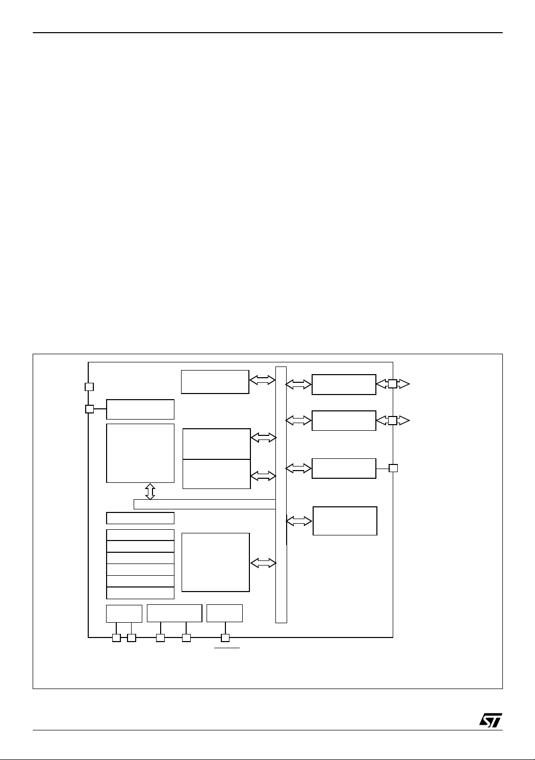
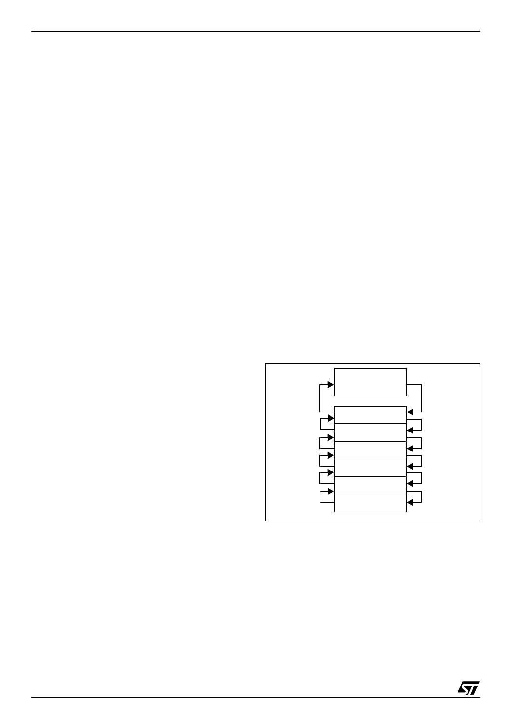
Figure 1. Block Diagram
8-BIT *
V
PP
A/D CONVERTER
mable option bytes of the OTP/EPR OM versions
in the ROM option list (See Section 11.6 on page
96).
The ST62P08C/P09C/P10C/P20C are the Factory
Advanced Service Technique ROM (FASTROM)
versions of ST62T08C, T09C, T10C and T20C
OTP devices.
They offer the same functionality as OTP devices,
but they do not have to be programmed by the
customer (See Section 11 on page 90).
These compact low -cost devices feature a Timer
comprising an 8-bit counter with a 7-bit programmable prescaler, an 8-bit A/D Converter with up to
8 analog inputs (depending on device) and a Digital Watchdog timer, making them well suited for a
wide range of automotive, appliance and industrial
applications.
For easy reference, all parametric data are located
in Section 11 on page 90.
PORT A
PA0..PA3 (20mA Sink)
NMI
* Depending on device. P l ease refer to I/O Port section.
INTERR UPTS
PROGRAM
:
MEMORY
(1K, 2K
or 4K Bytes)
PC
STACK LEVEL 1
STACK LEVEL 2
STACK LEVEL 3
STACK LEVEL 4
STACK LEVEL 5
STACK LEVEL 6
POWER
SUPPLY
V
DDVSS
OSCILLATOR
OSCin OSCout RESET
DATA RO M
USER
SELECTABLE
DATA RAM
64 Bytes
8-BIT CO RE
RESET
PORT B
TIMER
WATCHDOG
TIMER
PB0..PB7 / Ain*
TIMER
6/104
4
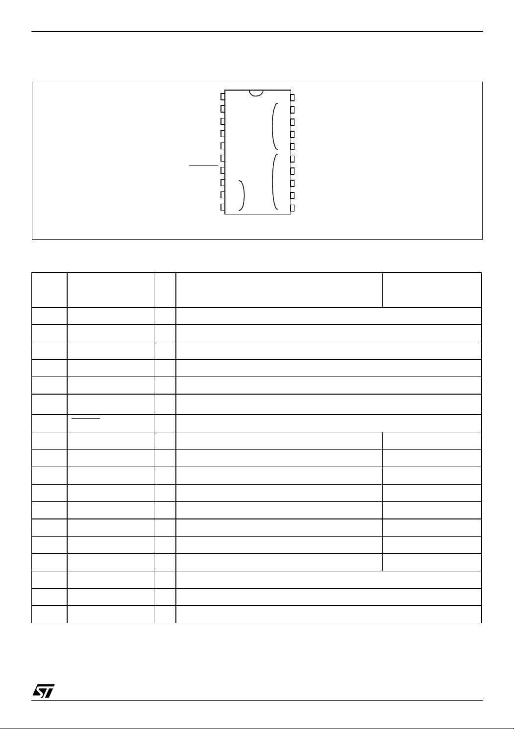
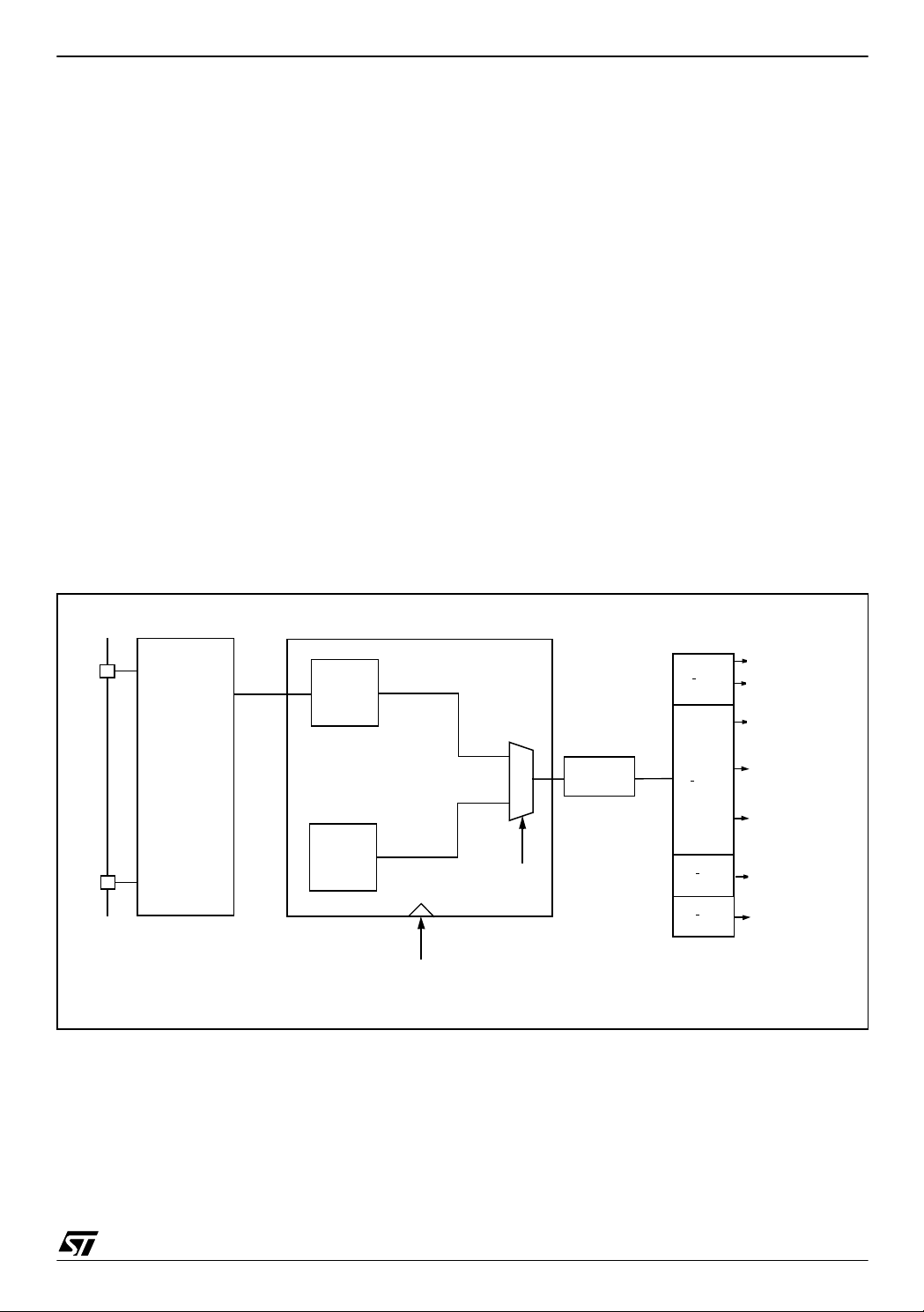
2 PIN DESCRI PTION
Figure 2. 20-Pin Package Pinout
ST6208C/ST6209C/ST6210C/ST6220C
V
DD
TIMER
OSCin
OSCout
NMI
V
PP
RESET
Ain*/PB7
Ain*/PB6
Ain*/PB5
itX associated interrupt vector
* Depending on device. Please refer to I/O Port secti on.
1
2
3
4
5
6
7
8
9
10
it1
it2
it2
V
20
SS
PA0/20mA Sink
19
PA1/20mA Sink
18
PA2/20mA Sink
17
16
PA3/20mA Sink
15
PB0/Ain*
14
PB1/Ain*
13
PB2/Ain*
12
PB3/Ain*
PB4/Ain*
11
Table 1. Device Pin Description
Pin n° Pin Name
1 V
DD
TIMER
2
Type
S Main power supply
I/O Timer input or output
3 OSCin I External clock input or resonator oscillator inverter input
4 OSCout O Resonator oscillator inverter output or resistor input for RC oscillator
Main Function
(after Reset)
Alternate Function
5 NMI I Non maskable interrupt (falling edge sensitive)
6V
PP
7 RESET
I/O Top priority non maskable interrupt (active low)
Must be held at Vss for normal operation, if a 12.5V level is applied to the pin
during the reset phase, the device enters EPROM programming mode.
8 PB7/Ain* I/O Pin B7 (IPU) Analog input
9 PB6/Ain* I/O Pin B6 (IPU) Analog input
10 PB5/Ain* I/O Pin B5 (IPU) Analog input
11 PB4/Ain* I/O Pin B4 (IPU) Analog input
12 PB3/Ain* I/O Pin B3 (IPU) Analog input
13 PB2/Ain* I/O Pin B2 (IPU) Analog input
14 PB1/Ain* I/O Pin B1 (IPU) Analog input
15 PB0/Ain* I/O Pin B0 (IPU) Analog input
16 PA3/ 20mA Sink I/O Pin A3 (IPU)
17 PA2/ 20mA Sink I/O Pin A2 (IPU)
18 PA1/ 20mA Sink I/O Pin A1 (IPU)
7/104
5

ST6208C/ST6209C/ST6210C/ST6220C
Pin n° Pin Name
19 PA0/ 20mA Sink I/O Pin A0 (IPU)
20 V
SS
Type
S Ground
Main Function
(after Reset)
Alternate Function
Legend / Abbreviations for Table 1:
* Depending on device. Please refer to Section 7 "I/O PORTS" on page 37.
I = input, O = output, S = supply, IPU = input with pull-up
The input with pull-up configuration (reset state) is valid as long as the user software does not change it.
Refer to Section 7 "I/O PORTS" on page 37 for more details on the software configuration of the I/O ports.
8/104
6
ST6208C/ST6209C/ST6210C/ST6220C
3 MEMORY MAPS, PROGRAMMING MODES AND OPTION BYTES
3.1 MEMORY AND REGISTER MAPS
3.1.1 Introd uct i on
The MCU operates in three separate memory
spaces: Program space, Data space, and Stack
space. Operation in these three memory spaces is
described in the following paragraphs.
Figure 3. Mem ory Addressing Dia gram
PROGRAM SPACE
000h
PROGRAM
MEMORY
(see Figure 4
on page 10)
0FF0h
INTERRUPT &
RESET VECTORS
0FFFh
Briefly, Program space contains user program
code in OTP and user vectors; Data space contains user data in RAM and in OTP, and Stack
space accommodat es six levels of stack for subroutine and interrupt service routine nesting.
DATA SPACE
000h
RESERVED
03Fh
040h
DATA ROM
WINDOW
07Fh
080h
081h
082h
083h
084h
0BFh
0C0h
0FFh
X REGISTER
Y REGISTER
V REGISTER
W REGISTER
RAM
HARDWARE
CONTROL
REGISTERS
(see Table 2)
ACCUMULATOR
9/104
1

ST6208C/ST6209C/ST6210C/ST6220C
MEMORY MAP (Cont’d)
Figure 4. Program Memory Map
ST6208C, 09C ST6210C ST6220C
0000h
0AFFh
0B00h
0B9Fh
0BA0h
0F9Fh
0FA0h
0FEFh
0FF0h
0FF7h
0FF8h
0FFBh
0FFCh
0FFDh
0FFEh
0FFFh
NOT IMPLEMENTED
RESERVED
*
USER
PROGRAM MEMORY
1024 BYTES
RESERVED
*
INTERRUPT VECTORS
RESERVED
*
NMI VECTOR
USER RESET VECTOR
0000h
07FFh
0800h
087Fh
0880h
0F9Fh
0FA0h
0FEFh
0FF0h
0FF7h
0FF8h
0FFBh
0FFCh
0FFDh
0FFEh
0FFFh
NOT IMPLEMENTED
RESERVED
*
USER
PROGRAM MEMORY
1824 BYTES
RESERVED
*
INTERRUPT VECTORS
RESERVED
*
NMI VECTOR
USER RESET VECTOR
0000h
07Fh
080h
0F9Fh
0FA0h
0FEFh
0FF0h
0FF7h
0FF8h
0FFBh
0FFCh
0FFDh
0FFEh
0FFFh
RESERVED
*
USER
PROGRAM MEMORY
3872 BYTES
RESERVED
*
INTERRUPT VECTORS
RESERVED
*
NMI VECTOR
USER RESET VECTOR
(*) Reserved areas should be filled with 0FFh
10/104
1

MEMORY MAP (Cont’d)
3.1.2 Program Space
Program Space comprises the instructions to b e
executed, the data required for immediate addressing mode instructions, the reserved factory
test area and the user v ectors. Program Space is
addressed via the 12-bit Program Counter register
(PC register). Thus, the MCU is capable of addressing 4K bytes of memory directly.
3.1.3 Readout Protection
The Program Memory in OTP, EPROM or ROM
devices can be protected against external readout
of memory by setting the Readout Protection bit in
the option bytes (S ecti on 3.3 on page 16).
In the EPROM parts, Readout Protection option
can be desactivated only by U.V. erasure that also
results in the whole EPROM context being erased.
Note: Once the Readout Protection is activated, it
is no longer possible, even for STMicroelectronics,
to gain access to the OTP or RO M contents. Returned parts can therefore n ot be accepted if the
Readout Protection bit is set.
3.1.4 Data Space
Data Space accommodates all the data necessary
for processing the user program. This space comprises the RAM resource, the proc essor core an d
peripheral registers, as well as read-only data
ST6208C/ST6209C/ST6210C/ST6220C
such as constants and look-up tables in OTP/
EPROM.
3.1.4.1 Data ROM
All read-only data is physically stored in program
memory, which also accommodates the Program
Space. The program m emory consequently contains the program code to be executed, as well as
the constants and look-up tables required by t he
application.
The Data Space locations in which the different
constants and look-up tables are addressed by the
processor core may be thought of as a 64-byte
window through which it is possible to acc ess the
read-only data stored in OTP/EPROM.
3.1.4.2 Data RAM
The data space includes the user RAM area, the
accumulator (A), the indirect registers (X), (Y), the
short direct registers (V), (W), the I/O port registers, the peripheral data and control registers, the
interrupt option register and the Data ROM Window register (DRWR register).
3.1.5 Stack Space
Stack space consists of six 12-bit registers which
are used to stack subroutine and interrupt return
addresses, as well as the current program counter
contents.
11/104
1
ST6208C/ST6209C/ST6210C/ST6220C
MEMORY MAP (Cont’d)
Table 2. Hardware Register Map
Address Block
080h
to 083h
0C0h
0C1h
0C2h
0C3h
0C4h
0C5h
0C6h
0C7h
0C8h CPU IOR Interrupt Option Register xxh Write-only
0C9h ROM DRWR Data ROM Window register xxh Write-only
0CAh
0CBh
0CCh
0CDh
0CEh
0CFh
0D0h
0D1h
CPU X,Y,V,W
I/O Ports
I/O Ports
I/O Ports
4)
ADC
Register
Label
1) 2) 3)
DRA
1) 2) 3)
DRB
DDRA
DDRB
2)
ORA
2)
ORB
ADR
ADCR
2)
X,Y index registers
V,W short direct registers
Port A Data Register
Port B Data Register
Reserved (2 Bytes)
Port A Direction Register
2)
Port B Direction Register
Reserved (2 Bytes)
Reserved (2 Bytes)
Port A Option Register
Port B Option Register
Reserved (2 bytes)
A/D Converter Data Register
A/D Converter Control Register
Register Name
Reset
Status
xxh R/W
00h
00h
00h
00h
00h
00h
xxh
40h
Remarks
R/W
R/W
R/W
R/W
R/W
R/W
Read-only
Ro/Wo
0D2h
0D3h
0D4h
0D5h
to 0D7h
0D8h
0D9h
to 0FEh
0FFh CPU A Accumulator xxh R/W
Timer1
Watchdog
Timer
PSCR
TCR
TSCR
WDGR Watchdog Register 0FEh R/W
Timer 1 Prescaler Register
Timer 1 Downcounter Register
Timer 1 Status Control Register
Reserved (3 Bytes)
Reserved (38 Bytes)
7Fh
0FFh
00h
R/W
R/W
R/W
Legend:
x = undefined, R/W = Read/Write, Ro = Read-only Bit(s) in the register, Wo = Write-only Bit(s)
in the register.
Notes:
1. The contents of the I/O p ort D R registers are read able only in output configuration. In i nput c onfiguration, the values of the I/O pins are returned instead of the DR register contents.
2. The bits associated with unavailable pins must always be kept at their reset value.
3. Do not use single-bit instructions (SET, RES...) on Port Data Registers if any pin of the port is configured
in input mode (refer to Section 7 "I/O PORTS" on page 37 for more details)
4. Depending on device. See device summary on page 1.
12/104
1
MEMORY MAP (Cont’d)
3.1.6 Data ROM Window
The Data read-only memory window is located
from address 0040h to address 007Fh in Data
space. It allows direct reading of 64 consecutive
bytes located anywhere in program memory, between address 0000h and 0FFFh.
There are 64 blocks of 64 bytes in a 4K device:
– Block 0 is related to the address range 0000h to
003Fh.
– Block 1 is related to the address range 0040h to
007Fh.
and so on...
All the program memory can therefore be used to
store either instructions or read-only data. The
Data ROM window can be moved in st eps of 64
bytes along the program memory by writing the
appropriate code in the Data ROM Window Register (DRWR).
ST6208C/ST6209C/ST6210C/ST6220C
3.1.6.1 Data ROM Window Register (DRWR)
The DRWR can be a ddressed li ke any RAM location in the Data Space.
This register is used to sele ct the 64-byt e blo ck of
program memory to be read in the Data ROM window (from address 40h to address 7Fh in Data
space). The DRWR register is not clea red on reset, therefore it must be written to before accessing the Data read-on ly memory window area for
the first time .
Address: 0C9h — Write Only
Reset Value = xxh (undefined)
70
- - DRWR5 DRWR4 DRWR3 DRWR2 DRWR1 DRWR0
Figure 5. Data R OM Window
PROGRAM
SPACE
0000h
64-BYTE
ROM
0FFFh
DATA SPACE
000h
040h
07Fh
0FFh
DATA ROM
WINDOW
Bits 7:6 = Reserved, must be cleared.
Bit 5:0 = DRWR[5:0]
dow Register Bits.
Data read-only memory Win-
These are the Data read-only
memory Window bits that correspond to the upper
bits of the data read-only memory space.
Caution:
This register is undefined on reset, it is
write-only, therefore do not read it nor access it using Read-Modify-Write instructions (SET, RES,
INC and DEC).
13/104
1
ST6208C/ST6209C/ST6210C/ST6220C
MEMORY MAP (Cont’d)
3.1.6.2 Data ROM Window memory addressing
In cases where some data (look-up tables for example) are stored in program memory, reading
these data requires the use of the Data ROM window mechanism. To do this:
1. The DRWR register ha s to be loaded with the
64-byte block number where the data are located
(in program memory). This number also gives the
start address of the block.
2. Then, the offset address of the byte in th e Data
ROM Window (corresponding to the offset in the
64-byte block in program memory) has to be loaded in a register (A, X,...).
When the above two steps are completed, the
data can be read.
To understand how to determine the DRWR and
the content of th e register, please refer to t he example shown in Figure 6. I n any c ase t he c alcul a-
Figure 6. Data ROM Window Memory Addressing
tion is automatically hand led by the ST6 deve lopment tools.
Please refer to the user manual of the corres poding tool.
3.1.6.3 Recommendations
Care is required when handling the DRWR register as it is write only. For this reason, the DRWR
contents should not be chan ged while executing
an interrupt service routine, as the service routine
cannot save and then restore the register’s previous contents. If it is imp ossible to avoi d writing to
the DRWR during the interrupt service routine, an
image of the register must be saved in a RAM location, and each time the program writes to the
DRWR, it must also write to the image register.
The image register must be written first so that, if
an interrupt occurs between the two instructions,
the DRWR is not affected.
0000h
0400h
OFFSET
0421h
07FFh
PROGRAM SPACE
64 bytes
DATA
DATA SPACE
DATA
10h
000h
040h
061h
07Fh
DRWR
0FFh
OFFSET
21h
DATA address in Program memory : 421h
DRWR content : 421h / 3Fh (64) = 10H data is located in 64-bytes window number 10h
64-byte window start address : 10h x 3Fh = 400h
Register (A, X,...)content : Offset = (421h - 400h) + 40h ( Data ROM Window start address in data space) = 61h
14/104
1

3.2 PROGRAMMING MODES
ST6208C/ST6209C/ST6210C/ST6220C
3.2.1 Program Memory
EPROM/OTP programming mode is set by a
+12.5V voltage a pplied to the T EST/V
pin. The
PP
programming flow of the ST62T08C,T09C,T10C,
T20C and E20C is described in the User Manual of
the EPROM Programming Board.
Table 3. ST6208C/09C Program Memory M ap
Device Address Description
0000h-0B9F h
0BA0h-0F9F h
0FA0h-0FEF h
0FF0h-0FF7 h
0FF8h-0FFB h
0FFCh-0FFD h
0FFEh-0FFF h
Reserved
User ROM
Reserved
Interrupt Vectors
Reserved
NMI Interrupt Vector
Reset Vector
Table 4. ST6210C Program Memory M ap
Device Address Description
0000h-087F h
0880h-0F9F h
0FA0h-0FEF h
0FF0h-0FF7 h
0FF8h-0FFB h
0FFCh-0FFD h
0FFEh-0FFF h
Reserved
User ROM
Reserved
Interrupt Vectors
Reserved
NMI Interrupt Vector
Reset Vector
STMicroelectronics (please refer to Section 12 on
page 99).
3.2.2 EPROM Erasing
The EPROM devices can be erased by exposure
to Ultra Violet light. The characteristics of the MCU
are such that erasure begins when the memory is
exposed to light with a wave lengths shorter than
approximately 4000Å. It should be noted that sunlight and some types of fluorescent lamps have
wavelengths in the range 3000-4000Å.
It is thus recommended that the window of the
MCU packages be covered by an opaque label to
prevent unintentional erasure problems when testing the application in such an environment.
The recommended erasure procedure is exposure
to short wave u ltraviolet light whi ch have a wavelength 2537Å. The integrated dose (i.e. U.V. intensity x exposure time) for erasure should be a minimum of 30W-sec/cm
dosage is approximately 30 to 40 minutes using an
ultraviolet lamp with 12000µW/cm
2
. The erasure time with this
2
power rating.
The EPROM device should be placed within
2.5cm (1inch) of the lamp tubes during erasure.
Table 5. ST6220C Program Memory M ap
Device Address Description
0000h-007F h
0080h-0F9F h
0FA0h-0FEF h
0FF0h-0FF7 h
0FF8h-0FFB h
0FFCh-0FFD h
0FFEh-0FFF h
Reserved
User ROM
Reserved
Interrupt Vectors
Reserved
NMI Interrupt Vector
Reset Vector
Note: OTP/EPROM devices can be programmed
with the development tools available from
15/104
1

ST6208C/ST6209C/ST6210C/ST6220C
3.3 OPTION BYTES
Each device is available for production in user programmable versions (OTP) as well as in factory
coded versions (ROM). O TP d evices are shippe d
to customers with a default content (00h), while
ROM factory coded parts contain the code supplied by the customer. This implies that OTP devices have to be configured by the customer using
the Option Bytes while the ROM devices are factory-configured.
The two option b ytes allow t he hardware configuration of the microcontroller to be selected.
The option bytes have no address in the memory
map and can be accessed only in programming
mode (for example using a standard ST6 programming tool).
In masked ROM devices, the option bytes are
fixed in hardware by the ROM code (see Section
11.6.2 "ROM VE RSION" on pag e 98). It is ther e-
fore impossible to read the option bytes.
The option bytes can be only programmed once. It
is not possible to change the selected options after
they have been programmed.
In order to reach the power consumption value indicated in Section 10.4, the option byte must be
programmed to its default value. Otherwise, an
over-consumption will occur.
MSB OPTION BY TE
Bits 15:10 = Reserved, must be always cleared.
LSB OPTION BYTE
Bit 7 = PROTECT
Readout Protection.
This option bit enables or disables external access
to the internal program memory.
0: Program memory not read-out protected
1: Program memory read-out protected
Bit 6 = OSC
Oscillator s elec tion
.
This option bit selects the main oscillator type.
0: Quartz crystal, ceramic resonator or external
clock
1: RC network
Bit 5 = Reserved, must be always cleared.
Bit 4 = Reserved, must be always set.
Bit 3 = NMI PULL
NMI Pull-Up
on/off.
This option bit enables or disables the internal pullup on the NMI pin.
0: Pull-up disabled
1: Pull-up enabled
Bit 2 = TIM PULL
TIMER Pull-Up
on/off.
This option bit enables or disables the internal pullup on the TIMER pin.
0: Pull-up disabled
1: Pull-up enabled
Bit 9 = EXTCNTL
External STO P MO DE control.
0: EXTCNTL mode not available. STOP mode is
not available with the watchdog active.
1: EXTCNTL mode available. STOP mode is avail-
able with the watchdog active by setting NMI pin
to one.
Bit 8 = LVD
Low Voltage Detector
on/off
.
This option bit enable or disable the Low Voltage
Dete ctor (LVD ) feature.
0: Low Voltage Detector disabled
1: Low Voltage Detector enabled
MSB OPTION BYTE
15 8
EXT
CTL
Default
Value
16/104
Reserved
XXXXXXXXXXXXX X XX
Bit 1 = WDACT
Hardware or software watchdog.
This option bit selects the watchdog type.
0: Software (watchdog to be enabled by software)
1: Hardware (watchdog always enabled)
Bit 0 = OSGEN
Oscillator Safeguard
on/off.
This option bit enables or disables the oscillator
Safeguard (OSG) feature.
0: Oscillator Safeguard disabled
1: Oscillator Safeguard enabled
LSB OPTION BYTE
70
LVD
PRO-
OSC Res. Res.
TECT
NMI
PULL
TIM
PULLWDACT
OSG
EN
1
4 CENTRAL PRO CESSING UNIT
ST6208C/ST6209C/ST6210C/ST6220C
4.1 INTRODUCTION
The CPU Core of ST6 devices is independent of the
I/O or Memory conf iguration. As such, it may b e
thought of as an independent central processor
communicating with on-chip I/O, Memory and Peripherals via internal address, data, and control
buses.
4.2 MAIN FEATURES
■ 40 basic instructions
■ 9 main addressing modes
■ Two 8-bit index registers
■ Two 8-bit short direct registers
■ Low power modes
■ Maskable hardware interrupts
■ 6-level hardware stack
4.3 CPU REGISTERS
The ST6 Family CPU core features six registers and
three pairs of flags available to the programmer.
These are described in the following paragraphs.
Accumulator (A). The accumulator is an 8-bit
general purpose register used in all arithmetic calculations, logical operations, and data manipula-
tions. The accumulator can be addressed i n Data
Space as a RAM lo cation at address FFh. Thus
the ST6 can manipulate the accumulator just like
any other register in Data Space.
Index Registers (X, Y). Th ese two registers are
used in Indirect addressing mode as pointers to
memory locations in Data Space. They can also
be accessed in Direct, Short Direct, or Bi t Direct
addressing modes. They are mapped in Data
Space at addresses 80h (X ) and 81h (Y) an d can
be accessed like any other memory location.
Short Direct Registers (V, W). The se two registers are used in Short Direct addressing mode.
This means that the data stored in V or W can be
accessed with a one-byte instruction (four CPU cycles). V and W can also be accessed using Di rect
and Bit Direct addressing modes. They are
mapped in Data Space at addresses 82h (V) and
83h (W) and can be accessed like any other memory location.
Note: The X and Y registers can also be used as
Short Direct registers in the same way as V and W.
Program Counter (PC). The program counter is a
12-bit register which cont ains the address of the
next instruction to be executed by the c ore. This
ROM location may be an opc ode, an operand, or
the address of an operand.
Figure 7. CPU Registers
70
ACCUMULA T OR
RESET VALUE = xxh
70
X INDEX REGISTER
RESET VALUE = xxh
70
Y INDEX REGISTER
RESET VALUE = xxh
70
RESET VALUE = xxh
70
RESET VALUE = xxh
11
RESET VALUE = RESET VECTOR @ 0FFEh-0FFFh
V SHORT INDIRECT
W SHORT INDIRECT
0
PROGRAM COUNTER
REGISTER
REGISTER
SIX LEVEL
STACK
NORMAL FLAGS
INTERRUPT FLAGS
NMI FLAGS
x = Undefined value
CN ZN
CI ZI
CNMI ZNMI
17/104
1
ST6208C/ST6209C/ST6210C/ST6220C
CPU REGISTERS (Cont’d)
The 12-bit length allows the direct addressing of
4096 bytes in Program Space.
However, if the program space contains more than
4096 bytes, the additional memory in program
space can be addressed by using the Program
ROM Page register.
The PC value is incremented after reading the address of the current instruction. To execute relative
jumps, the PC and the offset are shifted through
the ALU, where they are added; the result is then
shifted back into the PC. The program counter can
be changed in the following ways:
– JP (Jump) instruction PC = Jump address
– CALL instruction PC = Call address
– Relative Branch InstructionPC = PC +/- offset
– Interrupt PC = Interrupt vector
– Reset PC = Reset vector
– RET & RETI instructions PC = Pop (stack)
– Normal instruction PC = PC + 1
Flags (C, Z). The ST6 CPU includes three pairs of
flags (Carry and Zero), each pair being associated
with one of the three normal modes of operation:
Normal mode, Interrupt mode and Non Maskabl e
Interrupt mode. Each pair consists of a CARRY
flag and a ZERO flag. One pair (CN, ZN) is u sed
during Normal operation, another pair is used during Interrupt mode (CI, ZI), and a third pair is used
in the Non Maskable Interrupt m ode (CNMI, ZNMI).
The ST6 CPU uses the pair of flags associated
with the current mode: as soon as an interrupt (or
a Non Maskable I nterrupt) is generated, the ST 6
CPU uses the Interrupt flags (or the NMI flag s) instead of the Normal flags. When the RETI instruction is executed, the previously used set of flags is
restored. It should be noted that ea ch flag s et can
only be addressed in its own context (Non Maskable Interrupt, Normal Interrupt or Main routine).
The flags are not cleared during context swi tching
and thus retain their status.
C : Carry flag.
This bit is set when a carry or a borrow occurs dur-
ing arithmetic operations; otherwise it is cleared.
The Carry flag is also set to the val ue of the bit
tested in a bit test instruction; it also participates in
the rotate left instruction.
0: No carry has occured
1: A carry has occured
Z : Zero flag
This flag is set if the result of the last arithmetic or
logical operation was equal to zero; otherwise it is
cleared.
0: The result of the last operation is different from
zero
1: The result of the last operation is zero
Switching between the three sets of flags is per-
formed automatically when an NMI, an interrupt or
a RETI instruction occurs. As NMI mode is automatically selected after the reset of the MCU, the
ST6 core uses the NMI flags first.
Stack. The ST6 CPU includes a true LIFO (Last In
First Out) hardware stack which eliminates the
need for a stack pointer. The stack consists of six
separate 12-bit RAM locations that do not belong
to the data space RAM area. When a subroutine
call (or interrupt request) oc curs, the contents of
each level are shifted into the next level down,
while the content of the PC is shifted into the first
level (the original contents of the sixth stack level
are lost). When a subroutine or interrupt return occurs (RET or RETI instructions), the first level register is shifted back into the PC and the value of
each level is popped back into the previous level.
Figure 8. Stack manipulation
PROGRAM
COUNTER
ON RETURN
FROM
INTERRUPT,
OR
SUBROUTINE
LEVEL 1
LEVEL 2
LEVEL 3
LEVEL 4
LEVEL 5
LEVEL 6
ON
INTERRUPT,
OR
SUBROUTINE
CALL
Since the accumulator, in common with all other
data space registers, is not stored in this stack,
management of these registers should be performed within the subroutine.
Caution: The stack will remain in its “deepest” position if more than 6 nested calls or interrupts are
executed, and consequently the last return address will be lost.
It will also remain in its highest position if the stack
is empty and a RET or RETI is executed. In this
case the nex t in s truc t io n w ill be ex e c ut e d.
18/104
1
5 CLOCKS, SUPPLY AND RESET
5.1 CLOCK SYSTEM
ST6208C/ST6209C/ST6210C/ST6220C
The main oscillator of the MCU can be driven by
any of these cl ock sourc es:
– external clock signal
– external AT-cut parallel-resonant crystal
– external ceramic resonator
– external RC network (R
NET
).
In addition, an on-chip Low Frequency Auxiliary
Oscillator (LFAO) is available as a back-up c lock
system or to reduce power consumption.
An optional Oscillator Safeguard (OSG) filters
spikes from the oscillator lines, and switches to the
LFAO backup oscillator in t he event of m ain oscillator failure. It also automatically limits the internal
clock frequency (f
to guarantee correct operation. These functions
) as a function of VDD, in order
INT
are illustrated in Figure 10, and Figure 11.
Figure 9. Clock Circuit Block Diagram
OSCILLATOR SAFEGUA RD (OSG)
f
OSC
OSG
filtering
Table 6 illustrat es var ious poss ible os cillator c on-
figurations using an external crystal or ceramic
resonator, an external clock input, an external resistor (R
), or the lowest cost solution using only
NET
the LFAO.
For more details on c onfiguring the c lock options,
refer to the Option Bytes section of this document.
The internal MCU clock frequency (f
) is divided
INT
by 12 to drive the T imer, the Wat chdog timer and
the A/D converter, by 13 to drive the CPU core and
the SPI and by 1 or 3 to drive the ARTIMER, as
shown in Figure 9.
With an 8 M Hz o s c illat o r, the fastes t CP U cycle is
therefore 1.625µs.
A CPU cycle is the smallest unit of time needed to
execute any operation (f or instance, to increment
the Program Counter). An instruction may require
two, four, or five CPU cycles for execution.
:
13
SPI
CORE
8-BIT TIMER
MAIN
OSCILLATOR
0
1
LFAO
OSCOFF BIT
(ADCR REGISTER)
OSG ENABLE OPTION BIT (See OPTION BYTE SECTION)
* Depending on device. Se e device summary on page 1.
Oscillator
Divider
*
f
INT
:
12
: 1
: 3
WATCHDOG
*
ADC
8-BIT ARTIMER
8-BIT ARTIMER
19/104
1
ST6208C/ST6209C/ST6210C/ST6220C
CLOCK SYSTEM (Cont’d)
5.1.1 Main Oscillator
The oscillator configuration is specified by selecting the appropriate option in the option bytes (refer
to the Option Bytes section of this document).
When the CRYSTAL/RESONATOR option is selected, it must be used with a quartz crystal, a ceramic resonator or an external signal provided on
the OSCin pin. When the RC NETWORK option is
selected, the system clock is generated by an external resistor (the capacitor is imple men ted internally).
The main oscillator can be turned off (when the
OSG ENABLED option is selected) by setting the
OSCOFF bit of the ADC Control Register (not
available on some devices). This will automatically
start the Low Frequency Auxiliary Oscillator
(LFAO).
The main oscillator can be turned off by resetting
the OSCOFF bit of the A/D Converter Control Register or by resetting the MCU. When the main oscillator starts there is a delay made up of the oscillator start-up delay period plus the duration of the
software instruction at a clock frequency f
Caution: It should be noted that when t he RC network option is selected, the accuracy of the frequency is about 20% so it may not be suitable for
some applications (For more details, please refer
to the Electrical Characteristics Section).
LFAO
.
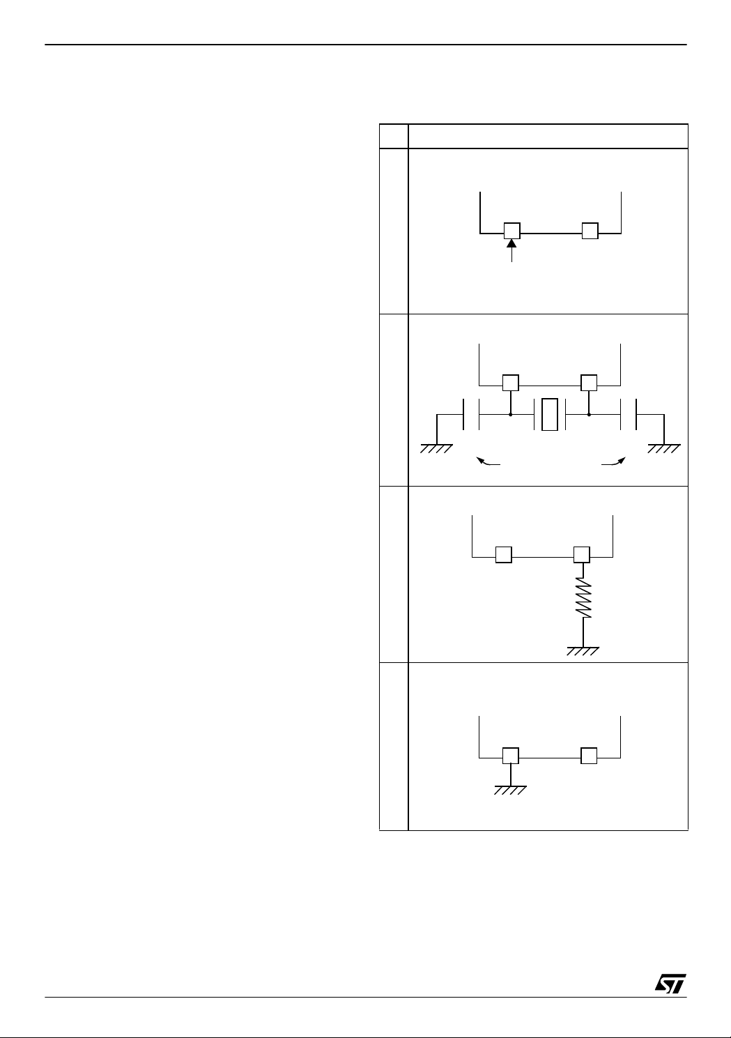
Table 6. Oscillator Configurations
Hardware Configuration
1)
Crystal/Resonator Option
1)
C
Crystal/Resonator Option
1)
External Clock
ST6
OSCin OSCout
NC
EXTERNAL
CLOCK
Crystal/Resonator Clock
OSCin OSCout
L1
OSCin OSCout
ST6
LOAD
CAPACITORS
RC Network
ST6
3)
2)
C
L2
NC
R
NET
RC Network Option
1)
OSG Enabled Option
Notes:
1. To select the options sho wn in column 1 of the abo ve
table, refer to the Option Byte section.
2.This schematic are given for guidance only and are subject to the schematics given by the crystal or ceramic resonator manufacturer.
3. For more details, plea se refer to the Electric al Char acteristics Section.
LFAO
ST6
OSCin OSCout
NC
20/104
1
CLOCK SYSTEM (Cont’d)
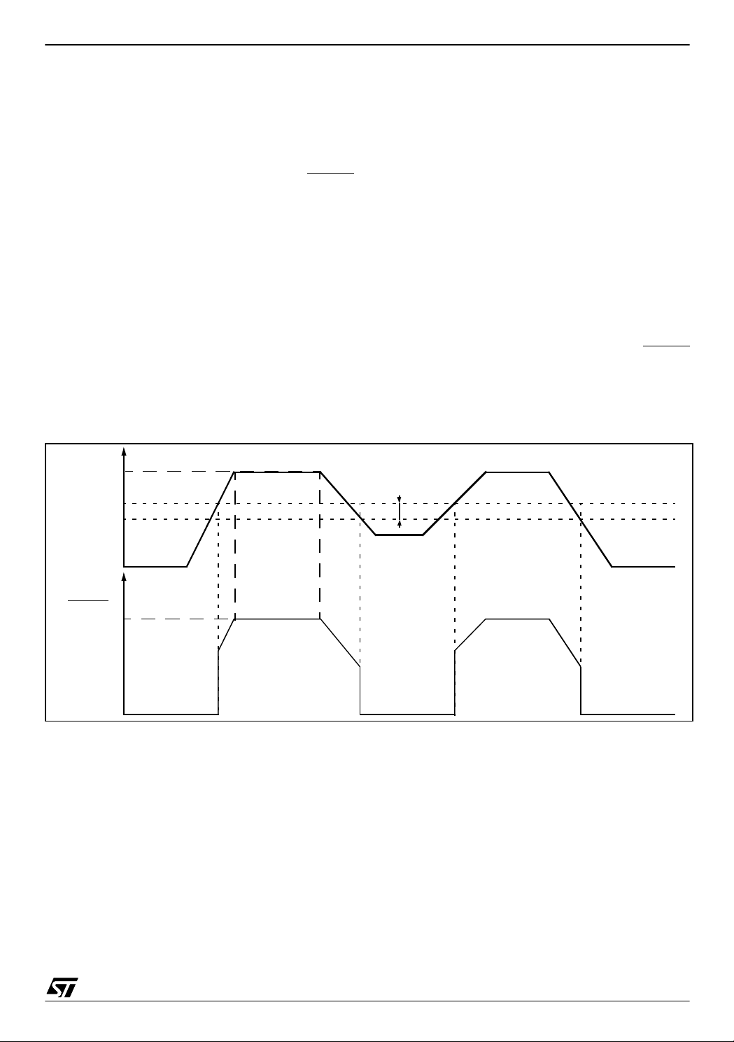
5.1.2 Oscillator Safeguard (OSG)
The Oscillator Safeguard (OSG) feature is a
means of dramatically improving the operational
integrity of the MCU. It is available when the OSG
ENABLED option is selected in the option byte (refer to the Option Bytes section of this document).
The OSG acts as a filter whose cross-over frequency is device dependent and provides three
basic functions:
– Filt er ing s pik e s on the os c illator lines whic h
would result in driving the CPU at excessive frequencies
– Manag eme nt of the Low Frequency Auxiliary
Oscillator (LFAO), (useable as low cost internal
clock source , backup clock i n ca se of main oscillator failure or for low power consumption)
– Automatically limiting the f
clock frequency as
INT
a function of supply voltage, to ensure correct
operation even if the power supply drops.
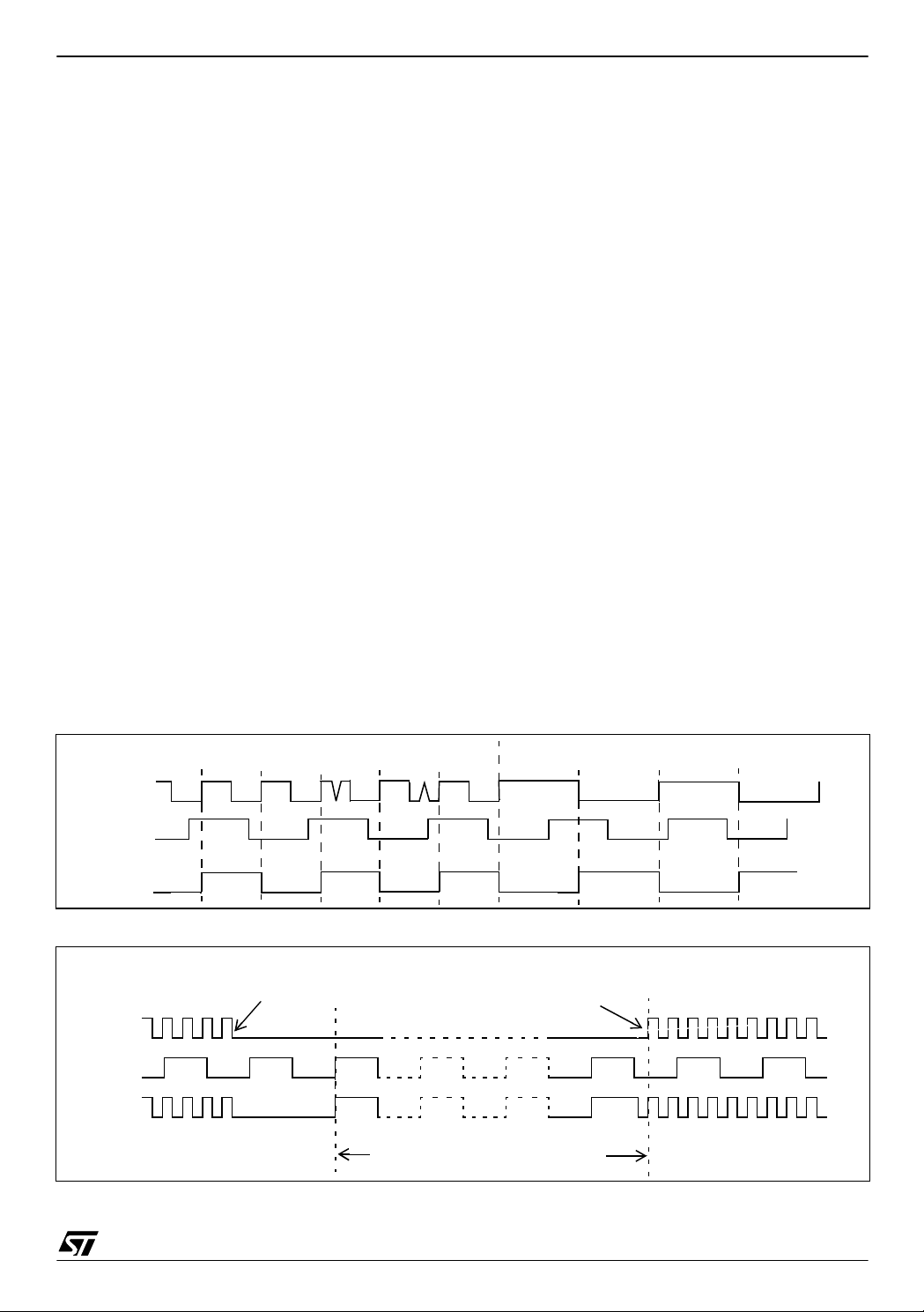
5.1.2.1 Spike Filtering
Spikes on the oscillator lines result in an effectively
increased internal clock frequency. In the absence
of an OSG circuit, this may lead to an over frequency for a given power supply voltage. The
OSG filters out such spikes (as illustrated in Figure
10). In all cases, when the OSG is active, the max-
ST6208C/ST6209C/ST6210C/ST6220C
imum internal clock frequency, f
, which is supply voltage dependent.
f
OSG
5.1.2.2 Management of Supply Voltage
Variations
Over-frequency, at a given power supp ly level, is
seen by the OSG as spikes; it therefore filte rs out
some cycles in order that the internal clock frequency of the device is kept within the range t he
particular device can stand (depending o n V
and below f
: the maximum authorised frequen-
OSG
cy with OSG enabled.
5.1.2.3 LFAO Managemen t
When the OSG is enabled, the Low Frequency
Auxiliary Oscillator can be used (see Section
5.1.3).
Note: The OSG should be used wherever possible
as it provides maxim um security for the ap plication. It should be noted however, that it can increase power consumption and reduce the maximum operating frequency to f
Characteristics section).
Caution: Care has to be taken when using the
OSG, as the internal frequency is defined between
a minimum and a maximum value and may vary
depending on both V
cise timing measurement s, it is not recom men ded
and temperature. For pre-
DD
to use the OSG.
, is limited to
INT
(see Electrical
OSG
DD
),
Figure 10. OSG Filtering Function
f
OSC>fOSG
f
OSC
f
OSG
f
INT
Figure 11. LFA O Oscillator Funct i on
MAIN OSCILLATOR
STOPS
f
OSC
f
LFAO
f
INT
MAIN OSCILLA TOR
RESTARTS
INTERNAL CLOCK DRIVEN BY LFAO
f
OSC<fOSG
21/104
1

ST6208C/ST6209C/ST6210C/ST6220C
CLOCK SYSTEM (Cont’d)
5.1.3 Low Frequency Auxiliary Oscillator
(LFAO)
The Low Frequency Auxiliary Oscillator has three
main purposes. Firstly, it can be used to reduce
power consumption in non timing critical routines.
Secondly, it offers a fully integrated system clock,
without any external components. Lastly, it acts as
a backup oscillator in case of m ain oscillator failure.
This oscillator is available when the OSG ENABLED option is selected in the option byte (refer to
the Option Bytes section of this document). In this
case, it automatically starts one of its periods after
the first missing edge of t he m ain os cillator, whatever the reason for the failure (main oscillator defective, no clock circuit ry prov i ded, m ain o scillat or
switched off...). See Figure 11.
User code, normal interrupts, WAIT and STOP instructions, are processed as normal, at the reduced f
cy is decreased, since the internal frequency is below 1.2 MHz .
At power on, until the main oscillator starts, the reset delay counter is driven by the LFAO. If the
main oscillator starts before the 2048 cycle delay
has elapsed, it takes over.
frequency. The A/D converter accura-
LFAO
The Low Frequency Auxiliary Oscillator is automatically switched off as soon as the main oscillator starts.
5.1.4 Register Description
ADC CONTROL REGISTER (ADCR)
Address: 0D1h — Read/Write
Reset value: 0100 0000 (40h)
70
ADCR7ADCR6ADCR5ADCR4ADCR3OSC
Bit 7:3, 1:0 = ADCR[7:3], ADCR[1:0]
Register
.
ADCR1ADCR
OFF
ADC Control
0
These bits are used to control the A/D converter (if
available on the device) otherwise they are not
used.
Bit 2 = OSCOFF
Main Oscillator Off.
0: Main oscillator enabled
1: Main oscillator disabled
Note: The OSG must be enabled using the OSGEN option in the Opt ion Byte, otherw ise t he OSCOFF setting has no effect.
22/104
1
5.2 LOW VOLTAGE DETECTOR (LVD)
ST6208C/ST6209C/ST6210C/ST6220C
The on-chip Low Voltage De tector is enabled by
setting a bit in the option bytes (refer to the Option
Bytes section of this document).
The LVD allows the device to be used without any
external RESET circuitry. In this ca se , th e RESET
pin should be left unconnected.
If the LVD is not used, an external circuit is mandatory to ensure correct Power On R eset operation,
see figure in the Reset section. For more details,
please refer to the application note AN669.
The LVD generates a static Reset when the supply
voltage is below a reference value. This means
that it secures the power-up as well as the powerdown keeping the ST6 in reset.
The V
than the V
reference value for a voltage drop is lower
IT-
reference value for power-on in order
IT+
to avoid a parasitic reset when the MCU starts running and sinks current on the supply (hysteresis).
Figure 12. Low Voltage Detector Reset
V
DD
V
IT+
V
IT-
The LVD Reset circuitry gene rates a reset when
V
is below:
DD
when VDD is rising
– V
IT+
– V
when VDD is falling
IT-
The LVD function is illustrated in Figur e 12.
If the LVD is enabled, the MCU can be in only one
of two states:
– Over the input threshold voltage, it is running un-
der full software control
– Below the input threshold voltage, it is in static
safe reset
In these conditions, secure operation is guaranteed without the need for external reset hardware.
During a Low Voltage Detector Reset, the RESET
pin is held low, thus p ermitting the MCU to reset
other devices.
V
hyst
RESET
23/104
1
ST6208C/ST6209C/ST6210C/ST6220C
5.3 RESET
5.3.1 Introd uct i on
The MCU can be reset in three ways:
■ A low pulse input on the RESET pin
■ Internal Watchdog reset
■ Internal Low Voltage Detector (LVD) reset
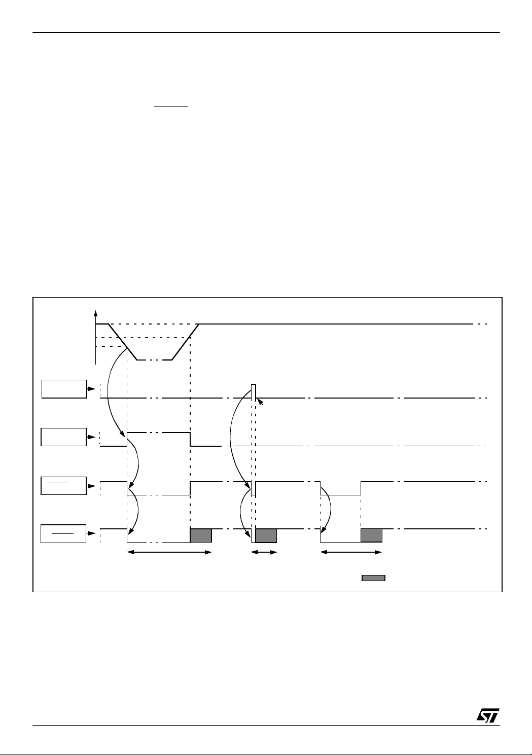
5.3.2 RESET Sequence
The basic RESET sequence consists of 3 main
phases:
■ Internal (watchdog or LVD) or external Reset
event
■ A delay of 2048 clock (f
■ RESET vector fetch
INT
) cycles
The reset delay allows the oscillator to stabilise
and ensures that recovery ha s taken place from
the Reset state.
Figure 13. RESET Sequence
V
DD
V
IT+
V
IT-
The RESET vector fetch phase duration is 2 clock
cycles.
When a reset occurs:
– The stack is cleared
– The PC is loaded with the address of the Reset
vector. It is located in program ROM starting at
address 0FFEh.
A jump to the beginning of the us er program m ust
be coded at this address.
– The interrupt flag is automatically set, so that the
CPU is in Non Maskable Interrupt mode. This
prevents the initialization routine from being interrupted. The initialization routine should therefore be terminated by a RETI instruction, in order
to go back to normal mode.
WATCHDOG
RESET
LVD
RESET
RESET PIN
INTERNAL
RESET
RUN
RESET
WATCHDOG UNDERFLOW
RUN RUN RUN
RESET RESET
2048 CLOCK CYCLE (f
INT
) DELAY
24/104
1
RESET (Cont’d)
5.3.3 RESET
The RESET
Pin
pin may be co nnecte d to a device on
the application board in order to reset the MCU if
required. The RESET
pin may be pulled low in
RUN, WAIT or STOP mode. This input can be
used to reset the internal state of the MCU and ensure it starts-up correctly. The pin, which i s connected to an internal pull-up, is active low and features a Schmitt trigger input. A delay (2048 clock
cycles) added to the external signal ensures that
even short pulses on the RESET
as valid, provided V
has completed its rising
DD
pin are accepted
phase and that the oscillator is running correctly
(normal RUN or WAIT modes). The MCU is kept in
the Reset state as long a s the RESET
pin is held
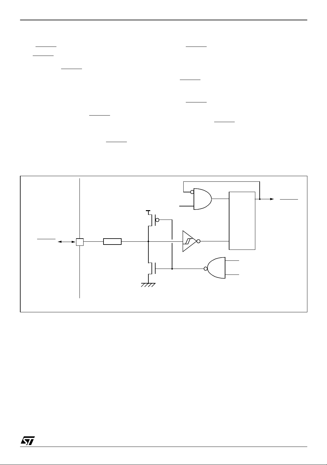
low.
Figure 14. Reset Block Diagram
ST6208C/ST6209C/ST6210C/ST6220C
If the RESET
RUN or WAIT modes, processing of the user program is stopped (RUN mode only), the I/O ports
are configured as inputs with pull-up resistors and
the main oscillator is restarted. When the level on
the RESET
quence is executed at the end of the internal delay
period.
If the RESET
STOP mode, the oscillator starts up and all the I/O
ports are configured as inputs with pull-up resistors. When the RESET
the initialization sequence is executed at th e end
of the internal delay period.
A simple external RESET circuitry is shown in Fig-
ure 15. For more details, please refer to the appli-
cation note AN669.
pin is grounded while the MCU is in
pin then goes high, the initialization se-
pin is grounded while the MCU is in
pin level then go es high,
RESET
1) Resistive ESD protection.
R
ESD
INTERNAL
f
V
DD
R
PU
1)
INT
COUNTER
clock cycles
2048
WATCHDOG RESET
LVD RESET
RESET
25/104
1
ST6208C/ST6209C/ST6210C/ST6220C
RESET (Cont’d)
5.3.4 Watchdog Reset
The MCU provides a Wat chdog timer function in
order to be able to recover from software hangups. If the Watchdog register is not refreshed before an end-of-count condition is reached, a
Watchdog reset is generated.
After a Watchdo g reset, the MCU resta rts in the
same way as if a Reset was generated by the RESET pin.
Note: When a watchdog reset occurs, the RESET
pin is tied low for very short time period, to flag the
reset phase. This time is n ot long enough to reset
external circuits.
For more details refer to the Watchdog Timer
chapter.
5.3.5 LVD Reset
Two different RESET sequences caused by the internal LVD circuitry can be distinguished:
■ Power-On RESET
■ Voltage Drop RESET
During an LVD reset, the RESET
when V
DD
<V
(rising edge) or VDD<V
IT+
edge).
For more details, refer to the LVD chapter.
Caution: Do not externally connect directly the
RESET
pin to VDD, this may cause damage to the
component in case of internal RESET (Watchdog
or LVD).
Figure 15. Simple External Reset Circuitry
pin is pulled low
(falling
IT-
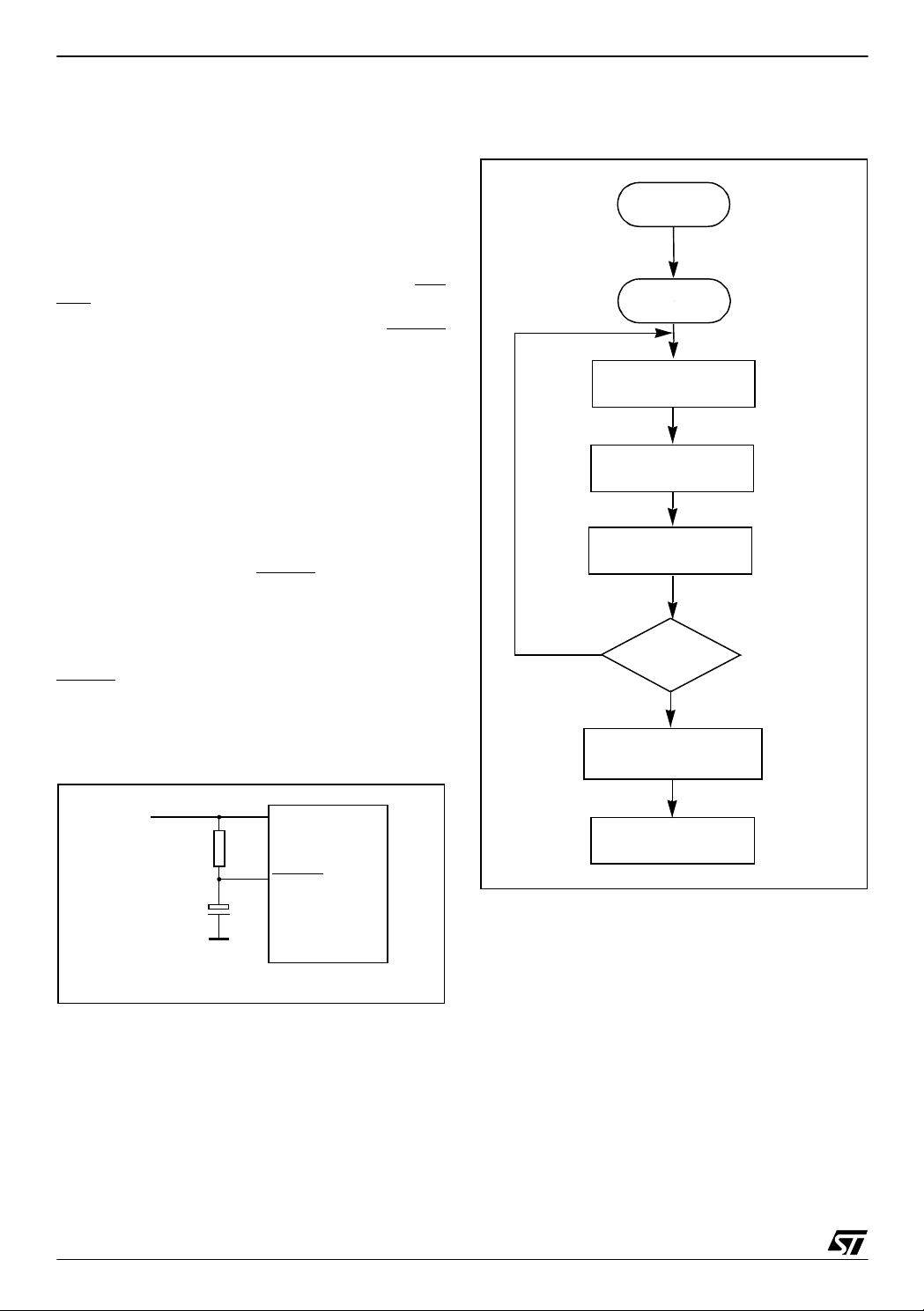
Figure 16. Reset Processing
RESET
CLOCK CYC LE
INTERNAL
RESET
NMI MASK SET
INT LATCH CLEARED
(IF PRESENT)
SELECT
NMI MODE FLA G S
PUT FFEh
ON ADDRESS BUS
YES
FROM RESET LOCATIONS
IS RESET STILL
PRESENT?
NO
LOAD PC
FFEh/FFFh
2048
DELAY
V
DD
Typical: R = 10K
C = 10nF
26/104
1
V
DD
R
RESET
C
ST62xx
R > 4.7 K
FETCH INSTRUCTION
5.4 INTERRUPTS
ST6208C/ST6209C/ST6210C/ST6220C
The ST6 core may be interrupted by four maskable interrupt sources, in addition to a Non Maskable Interrupt (NMI) source. The interrupt processing flowchart is shown in Figure 18.
Maskable interrupts must be enabled by setting
the GEN bit in the IOR register. However, even if
they are disabled (GEN bit = 0 ), interrupt events
are latched and may be processed as soon as the
GEN bit is set.
Each source is associated with a specific Interrupt
Vector, located in Program space (see Table 8). In
the vector location, the user must write a Jump in-
Figure 17. Inte rru pt s B l ock D i agra m
V
DD
NMI
PA0...PA3
I/O PORT REGISTER
“INPUT WITH INTER RUP T”
CONFIGURATION
LATCH
CLEARED BY H/W
AT START OF VECTOR #0 ROUTINE
LATCH
CLEARED BY H/W
AT START OF
VECTOR # 1 ROUTINE
struction to the associated interrupt service routine.
When an interrupt source generates an i nterrupt
request, the PC register is loaded with the address
of the interrupt vector, which then causes a Jum p
to the relevant interrupt service routine, thus servicing the int e r ru pt.
Interrupt are triggered by events either on external
pins, or from the on-chip peripherals. Several
events can be ORed on the same interrupt vector.
On-chip peripherals have flag registers to determine which event triggered the interrupt.
VECTOR #0
0
VECTOR #1
1
LES BIT
(IOR REGISTER)
EXIT FROM
STOP/WAIT
PB0...PB7
I/O PORT REGISTER
“INPUT WITH INTER RUP T”
CONFIGURATION
TIMER
(TSCR REGISTER)
A/D CONVERTER *
(ADCR REG I ST E R )
ESB BIT
(IOR REGISTER)
TMZ BIT
ETI BIT
EAI BIT
EOC BIT
CLEARED
BY H/W AT START OF
VECTOR #2 ROUTINE
* Depending on device. See device summary on page 1.
LATCH
VECTOR #2
VECTOR #3
VECTOR #4
GEN BIT
(IOR REGISTER)
27/104
1

ST6208C/ST6209C/ST6210C/ST6220C
5.5 INTERRUPT RULES AND PRIORITY MANAGEMENT
■ A Reset can interrupt the NMI and peripheral
interrupt routines
■ The Non Maskable Interrupt request has the
highest priority and can interrupt any peripheral
interrupt routine at any time but cannot interrupt
another NMI interrupt.
■ No peripheral interrupt can in terrupt another. If
more than one interrupt request is pending,
these are processed by the processor core
according to their priority level: vector #1 has the
highest priority while vector #4 the lowest. The
priority of each interrupt source is fixed by
hardware (see Interrupt Mapping table).
5.6 INTERRUPTS AND LOW POWER MODES
All interrupts cause the processor to exit from
WAIT mode. Only the external and som e specific
interrupts from the on-chip peripherals cause the
processor to exit from STOP mode (refer to the
“Exit from STOP“ column in the Interrupt Mapping
Table).
5.7 NON MASKABLE INTERRUPT
This interrupt is t riggered when a fallin g edge occurs on the NMI pin regardless of the state of the
GEN bit in the IOR register. An interrupt request
on NMI vector #0 is latched by a flip flop which is
automatically reset by the core at the beginning of
the NMI service routine.
5.8 PERIPHERAL INTERRUPTS
Different peripheral interrupt flags in the peripheral
control registers are able to cause an interrupt
when they are active if both:
– The GEN bit of the IOR register is set
– The corresponding enable bit is set in the periph-
eral control register.
Peripheral interrupts are linked to vectors #3 and
#4. Interrupt requests are flagged by a bit in their
corresponding control register. This means that a
request cannot be lost, because the flag bit m ust
be cleared by user software.
28/104
1

5.9 EXTERNAL INTERRUPTS (I/O Ports)
ST6208C/ST6209C/ST6210C/ST6220C
External interrupt vectors can be loaded into the
PC register if the corresponding external interrupt
occurred and if the GEN bit is set. These interrupts
allow the processor to exit from STOP mode.
The external interrupt polarity is selected t hrough
the IOR register.
External interrupts are linked to vectors #1 and #
2.
Interrupt requests on vector #1 can be configu red
either as edge or le vel-s ensitive us in g t he LES bit
in the IOR Register.
Interrupt requests from vector #2 are always edge
sensitive. The edge polarity can be configured using the ESB bit in the IOR Register.
In edge-sensitive mode, a latch is set when a edge
occurs on the interrupt source li ne and is cleared
when the associated interrupt routine is started.
So, an interrupt request can be stored until completion of the currently executing interrupt routine,
before being processed. If several interrupt requests occurs before comp let ion o f the cu rrent interrupt routine, only the first request is stored.
Storing of interrupt requests is not possible i n level
sensitive mode. To be taken into account, the lo w
level must be present on the interrupt pin when the
MCU samples the line after instruction execution.
5.9.1 Notes on using External Interrupts
ESB bit Spuri ous Interrupt on Ve c tor # 2
If a pin associated with interrupt vector #2 is configured as interrupt with pull-up, whenever vector
#2 is configured to be rising edge sensitive (by setting th e ESB b it in the I OR register ), a n interrupt i s
latched although a rising edge may not have occured on the associated pin.
This is due to the vector #2 circuitry.The workaround is to discard this first interrupt request in the
routine (using a flag for example).
Masking of One Interrupt by Another on Vector
#2.
When two or more port pins (associated with interrupt vector #2) are configured together as input
with int errupt (falling edge sensitive ), as long as
one pin is stuck at '0', the other pin can never generate an interrupt even if an act ive edge occurs at
this pin. The same thin g occurs when one pin is
stuck at '1' and interrupt vector #2 is configured as
rising edge sensitive.
To avoid this the f irst pin must input a signal that
goes back up to '1' right after the falling edge. Otherwise, in the interrupt rou tine for the first pin, deactivate the “input with interrupt” mode using the
port control registers (DDR, OR, DR). An active
edge on another pin can then be latched.
I/O port Configuration Spurious Interrupt on
Vector #2
If a pin associated with interrupt vector #2 is in ‘input with pull-up’ st ate, a ‘0’ level is present on t he
pin and the ESB bit = 0, when the I/O pin is configured as interrupt with pull-up by writing to the
DDRx, ORx and DRx register bits, an interrupt is
latched although a falling edge may not have occurred on the associated pin.
In the opposite case, if the pin is in interrupt with
pull-up state , a 0 level is present on the pin and
the ESB bit =1, when the I/O po rt is con figured as
input with pull-up by writing to the DDRx, ORx and
DRx bits, an interrupt is latched although a rising
edge may not have occurred on the associated
pin.
29/104
1
ST6208C/ST6209C/ST6210C/ST6220C
5.10 INTERRUPT HANDLING PROCEDURE
The interrupt procedure is very similar to a call procedure, in fact the user ca n consider the interrupt
as an asynchronous call procedure. As this is an
asynchronous event, the user cannot know the
context and the time at which it occurred. As a result, the user should save all Data space registers
which may be used within the interrupt routines.
The following list summarizes the interrupt procedure:
When an interrupt request occurs, the following
actions are performed by the MCU automatically:
– The core switches from the normal flags to the
interrupt flags (or the NMI flags).
– The PC contents are stored in the top level of the
stack.
– The normal interrupt lines are inhibited (NMI still
active).
– The internal latch (if any) is cleared.
– The associated interrupt vector is loaded in the PC.
When an interrupt request occurs, the following
actions must be performed by the user software:
– User selected registers have to be saved within
the interrupt service routine (normally on a soft-
ware stack).
– The source of the interrupt must be determined
by polling the interrupt flags (if more than one
source is associated with the same vector).
– The RETI (RETurn from Interrupt) instruction
must end the interrupt service routine.
After the RETI instruction is executed, the MCU re-
turns to the main routine.
Caution: When a maskable interrupt occurs while
the ST6 core is in NORMAL mode and during the
execution of an “ldi IOR, 00h” instruction (disabling
all maskable interrupts): if the interrupt request occurs during the first 3 cycles of the “ldi” instruction
(which is a 4-cycle instruction) the core will switch
to int errupt mo de BUT the flags CN and Z N will
NOT switch to the interrupt pair CI and ZI.
5.10.1 Interrupt Response Time
This is defined as the time between the mom ent
when the Program Counter is loaded wi th the interrupt vector and when the program has jump to
the interrupt subroutine and is ready to execute
the code. It depends on when t he in terrupt occurs
while the core is processing an instruction.
Figure 18. Interrupt Processing Flow Chart
INSTRUCTION
FETCH
INSTRUCTION
EXECUTE
INSTRUCTION
WAS
THE INSTRUCTION
YES
NORMAL MODE?
MASKABLE INTERRUPTS
THE STAC KED PC
NO
AN INTERRUPT REQUEST
AND INTERRUPT MASK?
*)
If a latch is present on the interrupt source line
?
A RETI
YES
IS THE CORE
ALREADY IN
NO
ENABLE
SELECT
NORMAL FLAGS
“POP”
IS THE R E AN
YES
NO
LOAD PC FROM
INTERRUPT VECTOR
CLEAR
INTERNAL LATCH
DISABLE
MASKABLE INTERRUPT
PUSH T H E
PC INTO T H E STACK
SELECT
INTERRUPT FLAGS
*)
Table 7. Interrupt Response Time
Minimum 6 CPU cycles
Maximum 11 CPU cycles
One CPU cycle is 13 exte rn al clock cycles thu s 1 1
CPU cycles = 11 x (13 /8M) = 17.875 µs with an 8
MHz external quartz.
30/104
1
 Loading...