

ST25TV02K ST25TV512
Datasheet
NFC Type 5 / RFID tag IC with up to 2-Kbit EEPROM, product identification and
protection
Features
Contactless interface
• Based on ISO/IEC 15693
• NFC Forum Type 5 tag certified by the NFC Forum
• Supports all ISO/IEC 15693 modulations, coding, subcarrier modes and data
rates
• Custom Fast read access up to 53 Kbit/s
• Single and multiple block reads
Wafer
• Single block writes
• Internal tuning capacitance: 23 pF, 99.7 pF
• Proprietary Inventory commands for speeding up the inventory process
Product status link
ST25TV02K
ST25TV512
Memory
• Up to 2 Kbits of EEPROM
• RF interface accesses blocks of four bytes
• Write time from RF: typical 5 ms for one block
• Data retention: 60 years
• Minimum endurance: 100 k write cycles
• 16-bit event counter with anti-tearing
Data protection
• User memory: two or three areas, read and/or write protected by two 32-bit
encrypted passwords for three areas or one 64-bit encrypted password for two
areas
• System configuration: write protected by a 32-bit encrypted password
• Permanent write locks at a block level
Product identification and protection
• Kill mode and untraceable mode
• Tamper detect capability (patent pending)
• TruST25 digital signature
• EAS (electronic article surveillance) capability
Privacy protection
• Consumer privacy can be protected through the following features:
– Kill mode
– Untraceable mode
• In association with:
– Passwords with cover coding
– Data and configuration locks (permanent or temporary)
Temperature range
• From - 40 to 85 °C
DS12074 - Rev 11 - February 2021
For further information contact your local STMicroelectronics sales office.
www.st.com

ST25TV02K ST25TV512
Package
• Sawn and bumped wafer, ECOPACK2 (RoHS compliant)
• 5-pin package, ECOPACK2 (RoHS compliant)
Compatibility ST25TV02K / LRI2K
• Full compatibility in terms of functionality and capacitances with two exceptions:
– Kill command requires option_flag to be set to 0
– Error codes and error generation can be different on a per command basis
DS12074 - Rev 11
page 2/90
1 Description
ST25TV02K and ST25TV512 are NFC/RFID tag ICs with a tamper-proof feature, and specific modes to protect
tag access, such as Untraceable mode.
These devices feature a digital signature used to prove the origin of the chip in cloning detection, embed a
configurable EEPROM with 60-year data retention, and can be operated from a 13.56 MHz long-range RFID
reader or an NFC phone.
The contactless interface is compatible with the ISO/IEC 15693 standard and NFC Forum Type 5 tag.
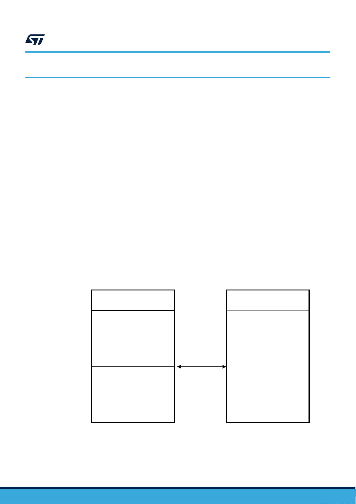
1.1 ST25TV02K/512 block diagram (with tamper detect)
Figure 1. ST25TV02K/512 (with tamper detect) block diagram
ISO 15693
ST25TV02K ST25TV512
Description
EEPROM
xxx-bit
256 bits
(EAS)
RF Tag
Long Range
256 bits
signature
2x32-bit password
(1)
TD
(tamper detect)
1. tamper detect is optional.
Table 1. Signal names
Signal name
AC0 Antenna coil I/O
AC1 Antenna coil I/O
TD0 Tamper detect loop I/O
TD1 Tamper detect loop I/O
Function Direction
DS12074 - Rev 11
page 3/90
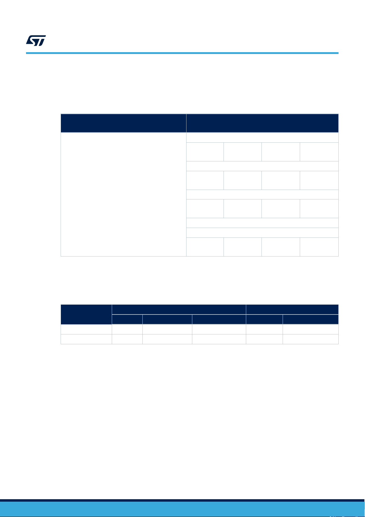
ST25TV02K ST25TV512
ST25TV02K/512 block diagram (with tamper detect)
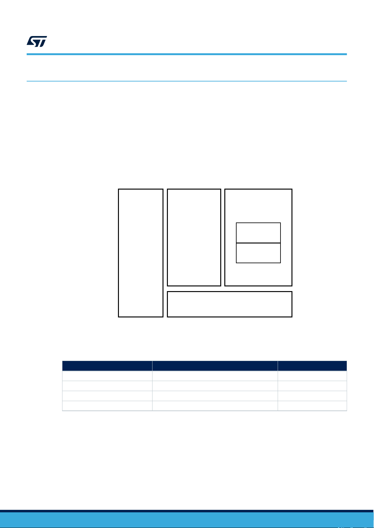
Figure 2. DFN5 package connections diagram (with tamper detect)
TD0
NC
AC0
1: Not Connected
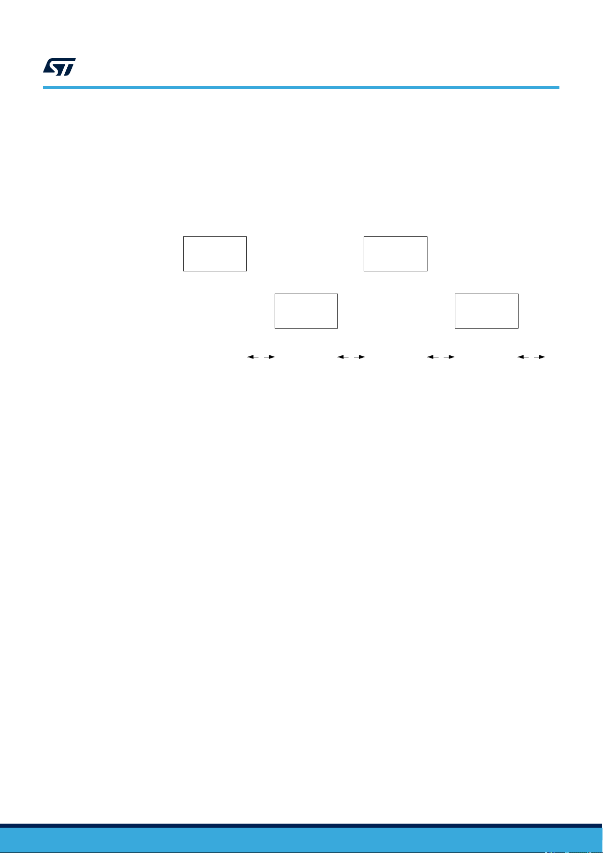
Figure 3. Die connections for sawn and bumped wafer (bottom view)
1
2
ABCD
XYZW
3 4
Top view
(marking side)
AC0 TD0
AC1 TD1
TD11
5
1
NC
2
AC1
5
2
Bottom view
(pads side)
AC0 NC
AC1 NC
With tamper detect Without tamper detect
1
2
34
DS12074 - Rev 11
page 4/90

2 Description of signals
2.1 Antenna coil (AC0, AC1)
These inputs are used exclusively to connect the ST25TV02K/512 devices to an external coil. It is advised not to
connect any other DC or AC path to AC0 or AC1.
When correctly tuned, the coil is used to power and access the device using the ISO/IEC 15693 and ISO 18000-3
mode 1 protocols.
2.2 Tamper detect (TD0, TD1)
These inputs are used to connect a wire loop to the ST25TV02K/512 devices to detect an open or a short
between the two pins TD0, TD1.
ST25TV02K ST25TV512
Description of signals
DS12074 - Rev 11
page 5/90
3 Power management
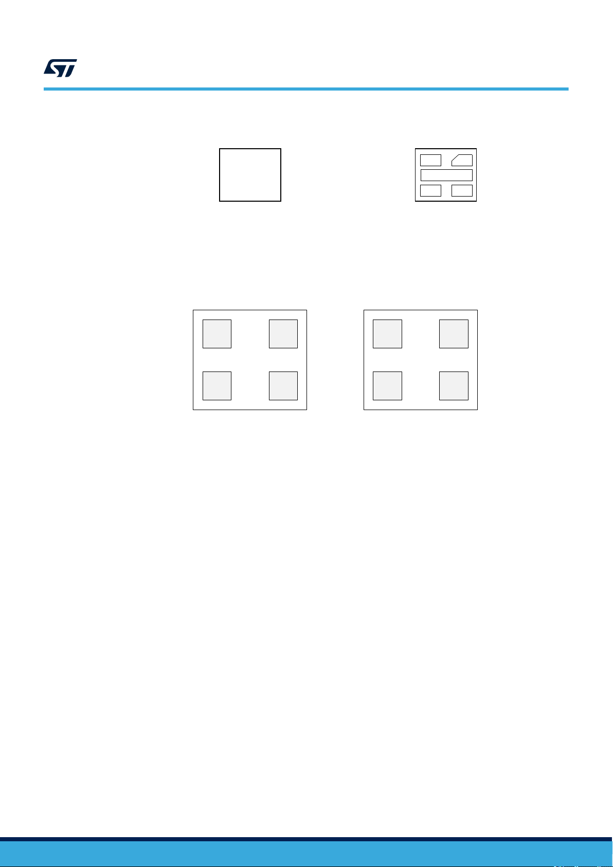
3.1 Device set
To ensure a proper boot of the RF circuitry, the RF field must be turned ON without any modulation for a minimum
period of time t
power-up sequence).
. Before this time, ST25TV02K/512 ignores all received RF commands. (See Figure 4. RF
boot_RF
ST25TV02K ST25TV512
Power management
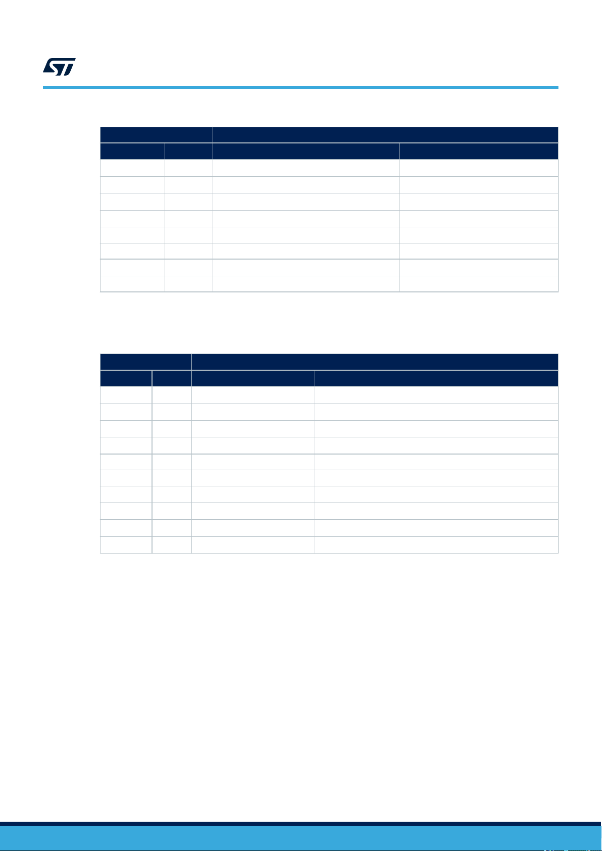
Figure 4. RF power-up sequence
RF interface ready
Power-up
by RF
3.2 Device reset
To ensure a proper reset of the RF circuitry, the RF field must be turned off (100% modulation) for a minimum
t
RF_OFF
period of time.
RFfield
Vint_supply
None Access
Allowed RF
t
boot_RF
RF REQUEST
RF ANSWER
DS12074 - Rev 11
page 6/90
4 Memory management
4.1 Memory organization overview
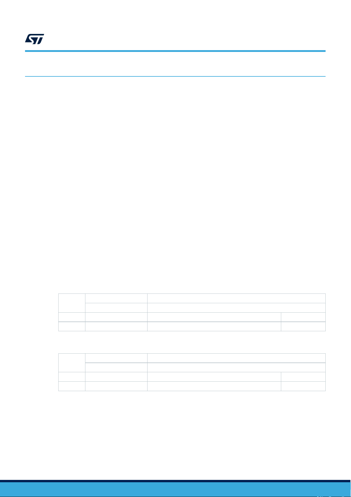
The ST25TV02K/512 memory is divided in two main memory areas:
• User memory
• System configuration area
The ST25TV02K/512 user memory can be divided into two or three user areas. Area 0 starts at address 0, it has
1 block size, it is always readable, and it can be locked.
The rest of the user memory can be either configured as one single area (Area 1) and can be read - and/or
- write-protected with one 64-bit password, or configured as two areas (Area 1 and Area 2), which can be
individually read - and/or - write-protected with a 32-bit password each. When Area 2 exists, Area 2 starts at the
block number corresponding to half the user memory.
Furthermore, each block can be locked permanently and individually for larger flexibility in number of areas
The ST25TV02K/512 system configuration area contains registers to configure all ST25TV02K/512 features,
which can be tuned by user. Its access is protected by a 32 bit configuration password.
This system configuration area also includes read only device information such as IC reference, memory size,
as well as a 64-bit block that is used to store the 64-bit unique identifier (UID), the AFI (default 00h) and DSFID
(default 00h) registers, the TruST25™ digital signature. The UID is compliant with the ISO 15693 description, and
its value is used during the anticollision sequence (Inventory). The UID value is written by ST on the production
line. The AFI register stores the application family identifier. The DSFID register stores the data storage family
identifier used in the anticollision algorithm.
The system configuration area includes blocks that store up to two RF user area access passwords and a RF
configuration password.
ST25TV02K ST25TV512
Memory management
Area 0:
1 block (always readable)
Area 1
User memory
(EEPROM up
to 2-Kbits)
Password
protected
Area 2
Note: Each block can be individually locked
Figure 5. Memory organization
Half user
memory
Area 0:
1 block (always readable)
Area 1
DS12074 - Rev 11
page 7/90
4.2 User memory
User memory is addressed as blocks of 4 bytes, starting at address 0. Table 2. 2Kb user memory as seen by RF
shows how memory is seen from RF interface.
ST25TV02K ST25TV512
User memory
Table 2. 2Kb user memory as seen by RF
RF command
(block addressing)
Read Single Block
Read Multiple Blocks
Fast Read Single Block
Fast Read Multiple Blocks
Write Single Block
Inventory Read
Fast Inventory Read
4.2.1 User memory areas
The user memory can be split into two or three different areas as showed in Table 3. Memory Organization
RF block 00h
Byte
0003h
RF block 01h
Byte
0007h
RF block 02h
Byte
0011h
....
RF block 3Fh
Byte
03FFh
Byte
0002h
Byte
0006h
Byte
0010h
Byte
03FEh
User memory
Byte
0001h
Byte
0005h
Byte
0009h
Byte
03FDh
Byte
0000h
Byte
0004h
Byte
0008h
Byte
03FCh
Part Number
ST25TV512
ST25TV02K Block 0 Block 1 to 31 Block 32 to 63 Block 0 Block 1 to 63
Area 0 Area 1 Area 2 Area 0 Area 1
Block 0 Block 1 to 7 Block 8 to 15 Block 0 Block 1 to 15
Each area has a distinct access privilege as explained below:
• Area 0 is always readable. It can be locked.
• Areas 1 and 2 can be protected in read and/or write access by password.
Each block of Areas 1 and 2 can be individually locked (see Section 5.2 Data protection).
4.3 System configuration area
In addition to the user memory, the ST25TV02K/512 include a set of registers located in the system configuration
area memory (EEPROM nonvolatile registers). These registers are set during device configuration (i.e.: area
extension), or by the application (i.e.: area protection)., their content is read during the boot sequence and defines
basic ST25TV02K/512 behaviour.
The registers located in the system configuration area can be accessed via dedicated Read Configuration and
Write Configuration commands, with a pointer acting as the register address.
The configuration security session must first be open, by presenting a valid configuration password, to grant write
access to system configuration registers.
Table 4 shows the complete map of the system configuration area.
Table 3. Memory Organization
Three areas configuration Two areas configuration
DS12074 - Rev 11
page 8/90
ST25TV02K ST25TV512
System configuration area
Table 4. System configuration memory map accessible through write_cfg and read_cfg commands
RF access Static Register
Address Type Name Function
00h
01h
02h
03h
04h RO Table 23. CNT_VAL Counter Value
05h RO Table 24. TAMPER_DETECT Tamper Detect
06h
07h RO Table 21. KID Key identifier
1. Write access is granted if RF configuration security session is open and configuration is not locked (LOCK_CFG register
equals to 0).
Table 5. System configuration memory map for registers accessed through dedicated commands
RW
RW
RW
RW
RW
(1)
(1)
(1)
(1)
(1)
Table 8. A1SS Area 1 access protection
Table 9. A2SS Area 2 access protection
Table 17. EAS_SEC EAS Security
Table 22. CNT_CFG Counter Configuration
Table 10. LOCK_CFG Configuration locked
RF access Static Register
Address Type Name Function
N/A
N/A
N/A
N/A
WO
WO
WO
WO
(1)
Table 25. LOCK_DSFID DSFID lock status
(2)
Table 26. LOCK_AFI AFI lock status
(1)
Table 27. DSFID DSFID value
(2)
Table 28. AFI AFI value
N/A RO Table 29. IC_REF IC reference value
N/A RO Table 30. UID Unique identifier, 8 bytes
WO
WO
WO
WO
(3)
Table 7. PWD_KILL Kill or untraceable password, 4 bytes
(4)
Table 12. PWD_A1 User Area 1 security session password, 4 bytes
(3)
Table 13. PWD_A2 User Area 2 security session password, 4 bytes
(3)
Table 11. PWD_CFG Configuration security session password, 4 bytes
N/A
N/A
N/A
N/A
1. Write access if DSFID is not locked
2. Write access if AFI is not locked.
3. Write access only if not locked.
4. Write access only if corresponding security session is open.
DS12074 - Rev 11
page 9/90
5 ST25TV02K/512 specific features
ST25TV02K/512 offer the data protection feature, both user memory and system configuration, a kill mode, and a
untraceable mode.
Those features can be programmed by setting registers of the ST25TV02K/512. ST25TV02K/512 can be partially
customized using configuration registers located in the EEPROM system area.
These registers are dedicated to:
• Data Memory organization and protection AiSS, LOCK_BLOCK.
• Kill mode, KILL
• The device’s structure LOCK_CFG
• Electronic Article Surveillance (EAS)
• TruST25™ digital signature
• Counter
• Tamper Detect
• Random Number generation
• Untraceable mode
A set of additional registers allows to identify and customize the product (DSFID, AFI, IC_REF, etc.).
Dedicated commands Read Configuration and Write Configuration must be used to access the configuration
registers. Update is only possible when the access right has been granted by presenting the configuration
password (PWD_CFG), and if the system configuration was not previously locked (LOCK_CFG=1).
After any valid write access to the configuration registers, the new configuration is immediately applied.
ST25TV02K ST25TV512
ST25TV02K/512 specific features
5.1
Kill mode
5.1.1 Kill registers
Table 6. KILL
RF
Bit Name Function Factory value
N/A KILL_MUTE Status of the KILL feature Inactive
RF
Bit Name Function Factory value
b31-b0 KILL_PSWD Password value for kill feature or untraceable mode 00000000h
Note: Refer to Table 5. System configuration memory map for registers accessed through dedicated commands .
Command Kill (cmd code A6h) UID @00h
Type WO if PWD_KILL is correctly presented in the Kill command.
Table 7. PWD_KILL
Command Write pswd (cmd code B1h) with pswd_id = 0h
Type WO: only possible if PWD_KILL is not locked.
DS12074 - Rev 11
page 10/90

5.1.2 Kill mode description
KILL register allows the user to permanently kill the ST25TV02K/512 tag.
Two working modes are offered by ST25TV02K/512:
• Kill mute mode:
– When KILL_MUTE is set with the Kill command code, the ST25TV02K/512 are killed. They can not be
read or written and stays mute to any request. Kill mute mode is definitive.
• Normal mode:
– In normal usage, KILL_MUTE is set to 0, ST25TV02K/512 will process the request and respond
accordingly.
The Kill Password PWD_KILL must be presented in the Kill command for setting the Kill Mute mode.
Kill Password lock
By default, the Kill password is not write protected. The kill password can be locked with Lock kill (cmd code B2h).
For safe operation, it is recommended to change the default value of the Kill Password and lock it even if not used
in the final product
When not used in an end application, a random value should be written into the KILL_PWD and the KILL_PWD
should be locked with Lock kill.
5.2 Data protection
ST25TV02K/512 provide a special data protection mechanism based on encrypted passwords that unlock
security sessions.
User memory can be protected for read and/or write access and system configuration can be protected from write
access. User memory can also be permanently locked. Each block can be independently locked from each other
with the Lock block command (refer to Section 6.4.8 Lock block).
ST25TV02K ST25TV512
Data protection
5.2.1 Data protection registers
Table 8. A1SS
RF
Bit Name Function Factory value
b1-b0 RW_PROTECTION_A1
b2 MEM_ORG
b7-b3 RFU - 00000b
Command
Type R always, W if configuration security session is open and configuration not locked
Read Configuration (cmd code A0h) @00h
Write Configuration (cmd code A1h) @00h
Area 1 access rights:
00: Area 1 access: Read is always allowed / Write always allowed
01: Area 1 access: Read is always allowed and if user security
session is open (i.e. the proper area 1 password has been presented),
write is allowed.
10: Area 1 access: Read and Write are allowed only if user security
session is open (the proper area 1 password has been presented).
11: Area 1 access: Read is allowed only if user security session is
open (the proper area 1 password has been presented). Write is
always forbidden.
0: memory is split in three areas (Areas 0, 1 and 2)
1: memory is composed of two areas (Areas 0 and 1)
00b
1b
Note: Refer to Table 4. System configuration memory map accessible through write_cfg and read_cfg commands
DS12074 - Rev 11
page 11/90

Table 9. A2SS
ST25TV02K ST25TV512
Data protection
RF
Bit Name Function Factory value
b1-b0 RW_PROTECTION_A2
b7-b2 RFU - 000000b
Command
Type R always, W if configuration security session is open and configuration not locked
Read Configuration (cmd code A0h) @01h
Write Configuration (cmd code A1h) @01h
Area 2 access rights:
00: Area 2 access: Read and write are always allowed
01: Area 2 access: Read is always allowed, and if the user
security session is open (i.e. the proper Area 2 password has been
presented), then write is allowed.
10: Area 2 access: Read and Write are allowed only if the user
security session is open (the proper Area 2 password has been
presented)
11: Area 2 access: Read is allowed only if user security session is
open (the proper Area 2 password has been presented). Write is
always forbidden.
00b
Note: Refer to Table 4. System configuration memory map accessible through write_cfg and read_cfg commands
Table 10. LOCK_CFG
Command
RF
Type
Bit Name Function Factory value
b0 LCK_CFG
b7-b1 RFU - 0000000b
Read Configuration (cmd code A0h) @06h
Write Configuration (cmd code A1h) @06h
R: always possible
W: if RF configuration security session is open (configuration password has been presented
before) and configuration not locked
0: Configuration is unlocked (configuration registers can be written)
1: Configuration is locked (configuration registers are definitively
locked)
0b
Note: Refer to Table 4. System configuration memory map accessible through write_cfg and read_cfg commands
Table 11. PWD_CFG
Command Write pswd (cmd code B1h) with pswd_id = 3h
RF
Bit Name Function Factory value
b31-b0 CFG_PSWD Password value for configuration area 00000000h
Type
WO: if RF configuration security session is open (configuration password has been presented
before). If the configuration is locked, and the EAS configuration is protected by password, the
new PWD_CFG value is only applicable to the EAS configuration.
Note: Refer to Table 5. System configuration memory map for registers accessed through dedicated commands
DS12074 - Rev 11
page 12/90
Table 12. PWD_A1
ST25TV02K ST25TV512
Data protection
RF
Bit Name Function Factory value
b31-b0 A1_PSWD
Command Write pswd (cmd code B1h) with pswd_id = 1h
Type WO: if RF area 1 security session is open (area 1 password has been presented before).
When MEM_ORG=0: Password value for user area 1
When MEM_ORG=1: 32 least significant bits of the 64-bit Password
value for user area 1
00000000h
Note: Refer to Table 5. System configuration memory map for registers accessed through dedicated commands
Table 13. PWD_A2
Command Write pswd (cmd code B1h) with pswd_id = 2h
RF
Bit Name Function Factory value
b31-b0 A2_PSWD
Type
WO: if RF area 2 security session is open (area 2 password has been presented before). Only
applicable to the case of MEMORG=0
When MEM_ORG=0: Password value for user area 2 in case of three
area memory setup
When MEM_ORG=1: 32 most significant bits of area 1 password in
case of two area memory setup
(in this last case area 1 password is 64-bit long)
00000000h
Note: Refer to Table 5. System configuration memory map for registers accessed through dedicated commands .
5.2.2 Passwords and security sessions
ST25TV02K/512 provide protection of user memory and system configuration registers. The users can access
those protected data by opening security sessions with the help of passwords. Access rights are more restricted
when security sessions are closed, and less restricted when security sessions are open.
There are two types of security sessions, as shown in Table 14:
Table 14. Security session type
Security session Open by presenting
user
configuration
1. Write access to the password number corresponding to the password number presented.
password Area 1, Area 2
(PWD_A1, PWD_A2)
Configuration password
(PWD_CFG)
In a three areas set up (MEM_ORG set at 0), each of the User Area 1 and 2 passwords is 32-bits long, and
default factory passwords value is 00000000h.
In a two areas setup (MEM_ORG set at 1), User Area 1 password is 64-bits long, and default factory password
value is 0000000000000000h.
The ST25TV02K/512 passwords management is organized around dedicated set of commands to access the
dedicated registers in system configuration area.
The dedicated password commands are:
• Write Password command (code B1h): See Section 6.4.20 Write Password.
• Present Password command (code B3h): See Section 6.4.21 Present Password
User possible actions for security sessions are:
Right granted when security session is open, and until it is
user access to protect user memory as defined in AiSS registers
user write access to password A1 or A2
user write access to configuration registers
closed
(1)
DS12074 - Rev 11
page 13/90
ST25TV02K ST25TV512
Data protection
• Open user security session: Present Password command, with password identifier 1 for PWD_A1 and 2
for PWD_A2 for three areas configuration or identifier 1 for PWD_A1 for two areas configuration, and the
valid corresponding password
• Write password:
– When MEMORG=0:
Present Password command, with password identifier 1 for PWD_A1 and 2 for PWD_A2 and the
current valid corresponding password. Then Write Password command, with same password number
(1 or 2) and the new corresponding password.
– When MEMORG=1:
present PWD_A1 (64 bits), then Write Password command with PWD_A1 and then PWD_A2
• Close user security session: Present Password command, with a different password number than the one
used to open session or any wrong password. Or remove tag from RF field (POR).
• Open configuration security session: Present Password command, with password number 3 and the valid
password PWD_CFG.
• Close configuration security session: Present Password command, with a password number different
than 3, or password number 3 and wrong password PWD_CFG. Or remove tag from field (POR).
Opening any new security session (user or configuration) automatically close the previously open one (even if it
fails).
Figure 6. Security sessions management
Present any
password not OK
Any other
command
Any other
command
PWD_x OK
Any other
command
Present
ST25TVxxx
out of RF field
Field ON
All security
sessions
closed
PWD_x OK
Security
session x
opened
(y closed)
Security
session y
opened
(x closed)
Field OFF
Present
Present
PWD_y OK
DS12074 - Rev 11
page 14/90

5.2.3 User memory protection
On factory delivery, areas are not protected.
Each area can be individually protected in read and/or write access.
Area 0 is always readable.
Furthermore, Area 0 can be independently write locked.
Each memory area can also have individual Read/Write access conditions.
For each area 1 and 2, an AiSS register is used to:
• Select the protection against read and write operations for this area
(See Table 8. A1SS, and Table 9. A2SS for details about available read and write protections).
When updating AiSS registers, the new protection value is effective immediately after the register write
completion.
• Block 0 is an exception to this protection mechanism:
– Block 0 can be individually write locked by issuing a Lock Single Block command. Once locked, it
cannot be unlock.
– User needs no password to lock block 0.
– Locking block 0 is possible even if the configuration is locked (LOCK_CFG=1).
– Unlocking Area 1 (through A1SS register) does not unlock block 0 if it has been locked though Lock
Block command.
– Once locked, the user cannot unlock block 0.
• Other blocks can be individually locked.
ST25TV02K ST25TV512
Data protection
Retrieve the security status of a user memory block or byte
User can read a block security status by issuing following commands:
• Get Multiple Blocks Security Status command
• (Fast) Read Single Block with option flag set to 1
• (Fast) Read Multiple Blocks with option flag set to 1
• (Fast) Inventory Read
ST25TV02K/512 responds with a Block security status containing a Lock_bit flag as specified in ISO 15693
standard. This lock_bit flag is set to 1 if block is locked against write.
Lock_bit flag value may vary if corresponding user security session is open or closed.
5.2.4 System memory protection
By default, the system memory is write protected, except the kill password and the EAS settings.
Th system memory consists of all the registers defined in Table 4. System configuration memory map accessible
through write_cfg and read_cfg commands. Some registers are read-only and can never be written.
To enable write access to system configuration registers, which have write capability, user must open the
configuration security session (by presenting a valid password 3) and system configuration must not be locked
(LOCK_CFG=00h).
By default, user can read all system configuration registers, except all passwords, LOCK_DSFID and LOCK_AFI.
Configuration lock:
• Write access to system configuration registers can be locked by writing 01h in the LOCK_CFG register.
• User cannot unlock system configuration if LOCK_CFG=01h, even after opening configuration security
session (Lock is definitive).
• When system configuration is locked (LOCK_CFG=01h), it is still possible to change passwords (0 to 3).
Device identification registers:
• AFI and DFSID registers can be independently locked by user, issuing respectively a Lock AFI and a Lock
DSFID command. Lock is definitive: once locked, AFI and DSFID registers cannot be unlocked.
• Other device identification registers (MEM_SIZE, BLK_SIZE, IC_REF, UID) are read only registers.
DS12074 - Rev 11
page 15/90
ST25TV02K ST25TV512
Untraceable mode
5.3 Untraceable mode
5.3.1 Untraceable mode register
Table 15. Untraceable mode register
Command Enable untraceable mode (cmd code BAh) with pswd_id = 0h
RF
Bit Name Function Factory value
b31-b0
Type
UNTRACEABLE
_MODE_PSWD
Note: Refer to Table 5. System configuration memory map for registers accessed through dedicated commands for the
untraceable mode register.
5.3.2 Untraceable mode description
With the EnableUntraceableMode command, the ST25TV02K/512 do not respond to any command except
Present Password and Get Random Number, guaranteeing the untraceability to customer requests.
The EnableUntraceableMode command requires the untraceable access code (fixed value) and the crypted
untraceable mode password to be presented for ST25TV02K/512 to enter into this mode.
To get out of the mode, the valid crypted untraceable mode password has to be transmitted to ST25TV02K/512
with the Present password command. The crypted untraceable mode password is obtained from the random
number and the untraceable mode password as explained in AN5103 "Password encryption for ST25TV512 and
ST25TV02K devices", available on www.st.com. When not used in an end application, a random value must be
written into the KILL_PWD password, and the KILL_PWD must be locked with Lock kill.
WO : only possible if untraceable mode password has been written before, always
writable otherwise
Password value for feature untraceable mode 00000000h
5.4 Random number
5.4.1 Random number register
Table 16. Random number register
RF
Bit Name Function Factory value
b15-b0 RANDOM_NUMBER 16-bit random number generated by ST25TV02K/512 N/A
Note: Refer to Table 5. System configuration memory map for registers accessed through dedicated commands for the
random number register.
5.4.2 Random number description
The GET_RANDOM_NUMBER returns a 16-bit random number.
Command Get random number (cmd code B4h)
Type RO: is only possible with Get random number command.
DS12074 - Rev 11
page 16/90

5.5 Electronic article surveillance (EAS)
5.5.1 EAS registers
Table 17. EAS_SEC
ST25TV02K ST25TV512
Electronic article surveillance (EAS)
Command
Type
Bit Name Function Factory value
b0 W_PROTECTION_EAS
b7-b1 RFU - 0000000b
Read Configuration (cmd code A0h) @02h
Write Configuration (cmd code A1h) @02h
R: always possible
W: if RF configuration security session is open (the proper configuration password has been
presented before) and configuration not locked
EAS security write protection:
0: EAS parameters are always writable
1: EAS parameters are write protected by configuration password.
In case of lock_EAS command has been previously used, this bit is
don’t care and EAS parameters are non-writable.
0b
Note: Refer to Table 4. System configuration memory map accessible through write_cfg and read_cfg commands for
the AES security activation register.
Table 18. EAS_TELEGRAM register
Enable EAS (cmd code A5h) with option flag set to 0
Command
RF
Type
Bit Name Function Factory value
b255-b0 EAS_TELEGRAM Electronic article surveillance telegram. All bits = 0b
Enable EAS (cmd code A5h) with option flag set to 1 and mask length ≠ 00h and EAS_ID
Write Single (cmd code 21h) to Blocks [248 to 255]
Read Single blocks at @248 to 255 returns an error.
R: possible with enable EAS command only if set EAS command has been presented before
W: possible under conditions set in the EAS_SEC configuration register and EAS
configuration not locked
(1)
1. Write Single Block at addresses 248 to 255 correspond to EAS blocks 1 to 8 respectively.
5.5.2 EAS ID
Table 19. EAS_ID
Command
RF
Type
Bit Name Function Factory value
b15-b0 EAS_ID Electronic article surveillance identifier value. 0000h
DS12074 - Rev 11
Enable EAS (cmd code A5h) with option flag set to 1 and mask length set to 0h
Write EAS ID (cmd code A7h)
R: possible with enable EAS command only if set EAS command has been presented before
W: possible under conditions set in the EAS_SEC configuration register and EAS
configuration not locked
page 17/90

ST25TV02K ST25TV512
Electronic article surveillance (EAS)
5.5.3 EAS configuration
Table 20. EAS_CFG
Enable EAS (cmd code A5h) with option flag set to 1 and mask length ≠ 00h and EAS_ID, or
Command
RF
Type
Bit Name Function Factory value
b1-b0 EAS_CFG
b15-b2 RFU - 000000b
The EAS parameters (ID, Telegram, mode (set/reset) can be definitely locked with the Lock EAS command (refer
to Section 6.4.27 Lock EAS).
with option flag set to 0
Write EAS config (cmd code A8h)
WO: possible under conditions set in the EAS_SEC configuration register and configuration
not locked
Electronic article surveillance identifier configuration:
00: 256 bit payload (EAS block 1 to 8)
01: 128 bit payload (EAS block 1 to 4)
10: 64 bit payload (EAS block 1 to 2)
11: 32 bit payload (EAS block 1)
00h
5.5.4 EAS description
The EAS (electronic article surveillance) feature is mainly used for library management, applications, requiring an
anti-theft protection.
This is programmable and configured by custom commands and optionally protected by the configuration
password (when programming EAS_SEC to 1) and can be locked.
A telegram can be stored using standard write command depending of its configured length (EAS block 1 – EAS
Block 8).
The EAS feature can be activated, reset, locked using a set of custom commands (see Section 6.4.24 Set EAS,
Section 6.4.25 Reset EAS, Section 6.4.26 Enable EAS, Section 6.4.27 Lock EAS, Section 6.4.28 Write EAS
ID and Section 6.4.29 Write EAS CONFIG).
The EAS feature is reset (deactivated) by default.
DS12074 - Rev 11
page 18/90
EAS – Normal
operation
ST25TV02K ST25TV512
Electronic article surveillance (EAS)
Figure 7. Nominal EAS operation
RF Reader ST25TV
EAS deactivated
(reset)
Optional
step
Write Single (EAS, EAS block x)
Write EAS config
Write EAS ID
Set EAS
Lock EAS
Enable EAS (selective ID or none)
If selected: EAS ID or telegram
Repeated
based on EAS
telegram size
EAS ready
DS12074 - Rev 11
Reset EAS (if not locked)
EAS deactivated
(reset)
By default, the EAS configuration (EAS telegram, EAS ID, EAS configuration, lock EAS, EAS mode) is not write
protected.
The EAS configuration can be write protected by the configuration password (PWD_CFG) by writing 1b1 into the
W_PROTECTION_EAS (EAS_SEC register). If W_PROTECTION_EAS bit is set, the EAS configuration can be
changed only if the configuration password has been presented just before in the same RF session.
Write access to the EAS configuration can be locked by executing the lock_EAS command. User cannot unlock
system configuration if the EAS configuration has already been locked earlier with the Lock_EAS command, even
after opening configuration security session (Lock is definitive).
page 19/90
ST25TV02K ST25TV512
TruST25 digital signature
5.6 TruST25 digital signature
ST25TV02K/512 support TruST25 digital signature, a feature that allows to verify the authenticity of the device,
based on a unique digital signature.
TruST25 solution encompasses secure industrialization processes and tools deployed by STMicroelectronics to
generate, store and check the signature in the device.
Table 21. KID
Command Read Cfg (cmd code A0h) @7h
Bit
b7-b0 KID
Type RO
Name Function Factory value
Contains a key identifier used for TruST25 digital signature
identification and possible revocation.
ST key number
Note: Refer to Table 4. System configuration memory map accessible through write_cfg and read_cfg commands for
the KID register.
5.7 Counter
5.7.1 Counter registers
Counter configuration
Table 22. CNT_CFG
Command
Bit
b0 CNT_EN
b1 CNT_CLR
b7-b2 RFU - 000000b
Type
Name Function Factory value
Read Cfg (cmd code A0h) @3h
Write Cfg (cmd code A1h) @3h
R: always possible
W: if RF configuration security session is open (the proper configuration password has been
presented before) and configuration not locked.
Counter enable
0: counter is disabled
1: counter is enabled on successful write operation (one increment
per RF session)
Counter clear:
0: don’t care
1: counter is cleared and automatically disabled (CNT_EN is put to 0)
This bit is self-cleared
0b
0b
Note: Refer to Table 4. System configuration memory map accessible through write_cfg and read_cfg commands for
the CNT_CFG register.
Counter value
Table 23. CNT_VAL
Bit
DS12074 - Rev 11
Command Read Cfg (cmd code A0h) @4h
page 20/90

ST25TV02K ST25TV512
Inventory Read
Bit
b15-b0 CNT_VAL Counter value 0h
Note: Refer to Table 4. System configuration memory map accessible through write_cfg and read_cfg commands for
the CNT_VAL register.
Type RO
Name Function Factory value
5.7.2 Counter description
A 16 bits counter can track the write events on the NDEF file.
It benefits from an anti-tearing mechanism that ensures the consistency of the counter, even if there is an
electrical problem during its increment.
The value of the counter (CNT_VAL) can be checked by any application, by reading the Counter register.
If enabled (when CNT_EN = 1), the Write counter will be incremented on first successful Write event which
is performed in the user area, inside an RF session (an RF session is entered when ST25TV02K/512 receive
enough power from the RF field). After enabling the counter, the counter will not count until the next RF field on/off
cycle.
The default configuration is with a counter disabled.
The counter cannot be locked. When the counter reach its maximum (216-1) the increment mechanism is blocked.
The counter is cleared and automatically disabled when CNT_CLR is set to 1.
Apart from these procedures, there is no way to act on the value of this counter.
The Read/Write counter can be configured through the Counter Configuration register.
This Counter Configuration register allows to:
• Enable or disable this counter (CNT_EN)
• Clear the counter (CNT_CLR)
The Counter Configuration register is protected by the configuration password.
5.8 Inventory Read
ST25TV02K/512 have the ability to perform in a single command Inventory Read (Refer to
Section 6.4.37 Inventory read), an Inventory in accordance with the regular anticollision sequence followed by
a Multiple Block Read, reducing the overall communication time. ST25TV02K/512 return the requested memory
content if ST25TV02K/512 match the mask specified in the command.
When using the Fast Inventory Read (refer to Section 6.4.38 Fast inventory read), the response is twice the data
rate.
5.9 Inventory Initiated
ST25TV02K/512 provide a special feature to improve the inventory time response of moving tags using the
Initiate_flag value. This flag, controlled by the Initiate command (refer to Section 6.4.36 Initiate), allows tags to
answer to Inventory Initiated commands (refer to Section 6.4.35 Inventory Initiated).
For applications where multiple tags are moving in front of a reader, it is possible to miss tags using the standard
inventory command. The reason is that the inventory sequence has to be performed on a global tree search. For
example, a tag with a particular UID value may have to wait the run of a long tree search before being inventoried.
If the delay is too long, the tag may be out of the field before it has been detected.
Using the Initiate command, the inventory sequence is optimized. When multiple tags are moving in front of a
reader, the ones which are within the reader field will be initiated by the Initiate command. In this case, a small
batch of tags will answer to the Inventory Initiated command which will optimize the time necessary to identify all
the tags. When finished, the reader has to issue a new Initiate command in order to initiate a new small batch of
tags which are new inside the reader field.
It is also possible to reduce the inventory sequence time using the Fast Initiate (refer to Section 6.4.34 Fast
Initiate), and Fast Inventory Initiated commands (refer to Section 6.4.33 Fast Inventory Initiated). These
commands allow the ST25TV02K/512 to increase their response data rate by a factor of 2, up to 53 kbit/s.
DS12074 - Rev 11
page 21/90
ST25TV02K ST25TV512
Tamper detect
5.10 Tamper detect
5.10.1 Tamper detect register
Tamper detection
Table 24. TAMPER_DETECT
Command Read Cfg (cmd code A0h) @5h
Bit
b0 TAMPER_DETECT
b7-b1 RFU - 000000b
Note: Refer to Table 4. System configuration memory map accessible through write_cfg and read_cfg commands for
the TAMPER_DETECT register.
Type RO
Name Function Factory value
State of Tamper:
0: loop is open. Tamper is detected
1: loop is closed. No tamper is detected
0b
5.10.2 Tamper detection description
The Tamper detection allows to check the shortage between the 2 TD0 and TD1 pins of the ST25TV02K/512.
This state TAMPER_DETECT is captured by ST25TV02K/512 each time that the ST25TV02K/512 are powered
and available upon demand by the reader using the Read Cfg command with CFG_ID 5. (Tamper detection)
This information will be lost during power off. (No permanent storage of the status.)
This is the customer responsibility to check the register status and behave accordingly.
The short impedance should be less than 50 Ω.
The tamper detect feature is available for the ST25TV02K/512-AD devices only. On other configurations, a Read
Cfg of the Tamper Detection register will return an error code.
If the two inputs pins TD0, TD1 are shorted with a wire at the time RF field is turned on, the tamper register will
have a value “1”. If TD0, TD1 are not shorted at the time RF field is turned on, the tamper register will have a
value “0”.
5.11 Device parameter registers
Command Lock DSFID (cmd code 2Ah)
Bit
b0 LOCK_DSFID
b7-b1 RFU - 0000000b
Type WO if DSFID not locked
Name Function Factory value
Table 25. LOCK_DSFID
0: DSFID is not locked
1: DSFID is locked
0b
Note: Refer to Table 5. System configuration memory map for registers accessed through dedicated commands for the
LOCK_DSFID register.
Table 26. LOCK_AFI
Bit
DS12074 - Rev 11
Command Lock AFI (cmd code 28h)
page 22/90
ST25TV02K ST25TV512
Device parameter registers
Bit
b0 LOCK_AFI
b7-b1 RFU - 0000000b
Type WO if AFI not locked
Name Function Factory value
0: AFI is not locked
1: AFI is locked
0b
Note: Refer to Table 5. System configuration memory map for registers accessed through dedicated commands for the
LOCK_AFI register.
Table 27. DSFID
Inventory (cmd code 01h)
Note:
Command
Bit
Type R always, W if DSFID not locked
Name Function Factory value
b7-b0 DSFID ISO/IEC 15693 Data Storage Format Identifier 00h
Refer to Table 5. System configuration memory map for registers accessed through dedicated commands for the
Get System Info (cmd code 2Bh)
Write DSFID (cmd code 28h)
DSFID register.
Table 28. AFI
Inventory (cmd code 01h)
Command
Bit
Type R always, W if AFI not locked
Name Function Factory value
b7-b0 AFI ISO/IEC 15693 Application Family Identifier 00h
Get System Info (cmd code 2Bh)
Write AFI (cmd code 27h)
Note: Refer to Table 5. System configuration memory map for registers accessed through dedicated commands for the
AFI register.
Table 29. IC_REF
Command Get System Info (cmd code 2Bh)
Bit
b7-b0 IC_REF ISO/IEC 15693 IC Reference 45h
Type RO
Name Function Factory value
Note: Refer to Table 5. System configuration memory map for registers accessed through dedicated commands for the
IC_REF register.
DS12074 - Rev 11
Bit
Table 30. UID
Command
Type RO
Name Function Factory value
Inventory (cmd code 01h)
Get System Info (cmd code 2Bh)
page 23/90

ST25TV02K ST25TV512
Device parameter registers
b7-b0
b7-b0 ISO/IEC 15693 UID byte 1
b7-b0 ISO/IEC 15693 UID byte 2
b7-b0 ISO/IEC 15693 UID byte 3
b7-b0 ISO/IEC 15693 UID byte 4
b7-b0 ISO/IEC 15693 UID byte 5: ST Product code 23h
b7-b0 ISO/IEC 15693 UID byte 6: IC Mfg code 02h
b7-b0 ISO/IEC 15693 UID byte 7 (MSB) E0h
UID
ISO/IEC 15693 UID byte 0 (LSB)
IC manufacturer
serial number
Note: Refer to Table 5. System configuration memory map for registers accessed through dedicated commands for the
UID register.
DS12074 - Rev 11
page 24/90

6 RF operations
Contactless exchanges are performed as specified by ISO/IEC 15693 and NFC Forum Type 5. The
ST25TV02K/512 communicate via the 13.56 MHz carrier electromagnetic wave on which incoming data are
demodulated from the received signal amplitude modulation (ASK: amplitude shift keying). The received ASK
wave is 10% or 100% modulated with a data rate of 1.6 Kbit/s using the 1/256 pulse coding mode or a data rate of
26 Kbit/s using the 1/4 pulse coding mode.
Outgoing data are generated by the ST25TV02K/512 load variation using Manchester coding with one or two
subcarrier frequencies at 423 kHz and 484 kHz. Data are transferred from the ST25TV02K/512 at 6.6 Kbit/s in low
data rate mode and 26 Kbit/s in high data rate mode. The ST25TV02K/512 support the 53 Kbit/s data rate mode
in one sub-carrier frequency at 423 kHz.
The ST25TV02K/512 follow ISO/IEC 15693 and NFC Forum Type 5 recommendation for radio-frequency power
and signal interface and for anticollision and transmission protocol.
6.1 RF communication
6.1.1 Access to a ISO/IEC 15693 device
ST25TV02K ST25TV512
RF operations
The dialog between the “reader” and the ST25TV02K/512 take place as follows:
These operations use the power transfer and communication signal interface described below (see Power
transfer, Frequency and Operating field). This technique is called RTF (Reader talk first).
• Activation of the ST25TV02K/512 by the operating field of the reader,
• Transmission of a command by the reader (ST25TV02K/512 detect carrier amplitude modulation)
• Transmission of a response by the ST25TV02K/512 (ST25TV02K/512 modulate is load clocked at subcarrier
rate)
Operating field
The ST25TV02K/512 operate continuously between the minimum and maximum values of the electromagnetic
field H defined in Table 153. RF characteristics. The Reader has to generate a field within these limits.
Power transfer
Power is transferred to the ST25TV02K/512 by radio frequency at 13.56 MHz via coupling antennas in the
ST25TV02K/512 and the Reader. The operating field of the reader is transformed on the ST25TV02K/512
antenna to an AC voltage which is rectified, filtered and internally regulated. During communications, the
amplitude modulation (ASK) on this received signal is demodulated by the ASK demodulator.
Frequency
The ISO 15693 standard defines the carrier frequency (fC) of the operating field as
13.56 MHz ± 7 kHz.
6.2
RF protocol description
6.2.1 Protocol description
The transmission protocol (or simply “the protocol”) defines the mechanism used to exchange instructions and
data between the VCD (Vicinity Coupling Device) and the VICC (Vicinity integrated circuit card) in both directions.
It is based on the concept of “VCD talks first”. The ST25TV02K/512 act as the VICC.
This means that a ST25TV02K/512 do not start transmitting unless it has received and properly decoded an
instruction sent by the VCD. The protocol is based on an exchange of:
• a request from the VCD to the ST25TV02K/512,
• a response from the ST25TV02K/512 to the VCD.
DS12074 - Rev 11
page 25/90
ST25TV02K ST25TV512
RF protocol description
Each request and each response are contained in a frame. The frames are delimited by a Start of Frame (SOF)
and End of Frame (EOF).
The protocol is bit-oriented. The number of bits transmitted in a frame is a multiple of eight (8), that is an integer
number of bytes.
A single-byte field is transmitted least significant bit (LSBit) first. A multiple-byte field is transmitted least
significant byte (LSByte) first and each byte is transmitted least significant bit (LSBit) first.
Figure 8. ST25TV02K/512 protocol timing
VCD
ST25TV02K/512
Timing
Request
frame
Response
frame
t
1
6.2.2 ST25TV02K/512 states referring to protocol
The ST25TV02K/512 can be in one of four states:
• Power-off
• Ready
• Quiet
• Selected
Transitions between these states are specified in Figure 9. state transition diagram and Table 31. response
depending on Request_flags.
Power-off state
Request
frame
Response
frame
t
2
t
1
t
2
DS12074 - Rev 11
The ST25TV02K/512 are in the power-off state when it does not receive enough energy from the VCD.
Ready state
The ST25TV02K/512 are in the Ready state when it receives enough energy from the VCD. When in the Ready
state, the ST25TV02K/512 answer any request where the Select_flag is not set.
Quiet state
When in the Quiet state, the ST25TV02K/512 answer any request with the Address_flag set, except for Inventory
requests.
Selected state
In the Selected state, the ST25TV02K/512 answer any request in all modes (see Section 6.2.3 Modes):
• Request in Select mode with the Select_flag set
• Request in Addressed mode if the UID matches
• Request in Non-Addressed mode as it is the mode for general requests
page 26/90
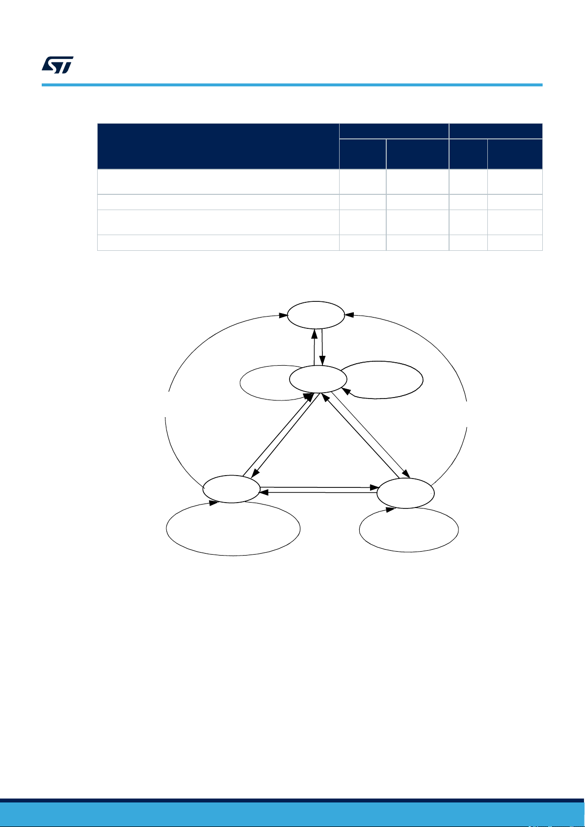
Table 31. response depending on Request_flags
Flags
ST25TV02K/512 in Ready or Selected state (Devices in Quiet state
do not answer)
ST25TV02K/512 in Selected state - X X -
ST25TV02K/512 in Ready, Quiet or Selected state (the device
which matches the UID)
Error (03h) or no response (command dependent) X - X -
Figure 9. state transition diagram
Power off
ST25TV02K ST25TV512
RF protocol description
Address_flag Select_flag
1
Addressed0Non addressed1Selected0Non selected
- X - X
X - - X
Out of field
after t
RF_OFF
Inventory
Out of RF field
after t
RF_OFF
Reset to ready
Quiet
Any other command where the
Address_Flag is set AND where
the Inventory_Flag is not set
Stay quiet(UID)
Select (UID)
1. The ST25TV02K/512 return to the Power Off state if the tag is out of the field for at least t
In RF field
Ready
Reset to ready where
Select_Flag is set or
Select with (# UID)
Stay quiet(UID)
Any other command
where Select_Flag
is not set
Select (UID)
Selected
Any other command
Out of RF field
after t
RF_OFF
RF_OFF
.
The intention of the state transition method is that only one ST25TV02K/512 should be in the Selected state at a
time.
When the Select_flag is set to 1, the request shall NOT contain a unique ID.
When the address_flag is set to 0, the request shall NOT contain a unique ID.
6.2.3 Modes
The term “mode” refers to the mechanism used in a request to specify the set of ST25TV02K/512 devices that
shall execute the request.
Addressed mode
When the Address_flag is set to 1 (Addressed mode), the request contains the Unique ID (UID) of the addressed
ST25TV02K/512.
DS12074 - Rev 11
page 27/90
 Loading...