ST25TV02KC ST25TV512C
Datasheet
NFC Type 5 / RFID tag IC with up to 2.5 Kbits of EEPROM, product identification
and protection
Features
Includes ST state-of-the-art patented technology
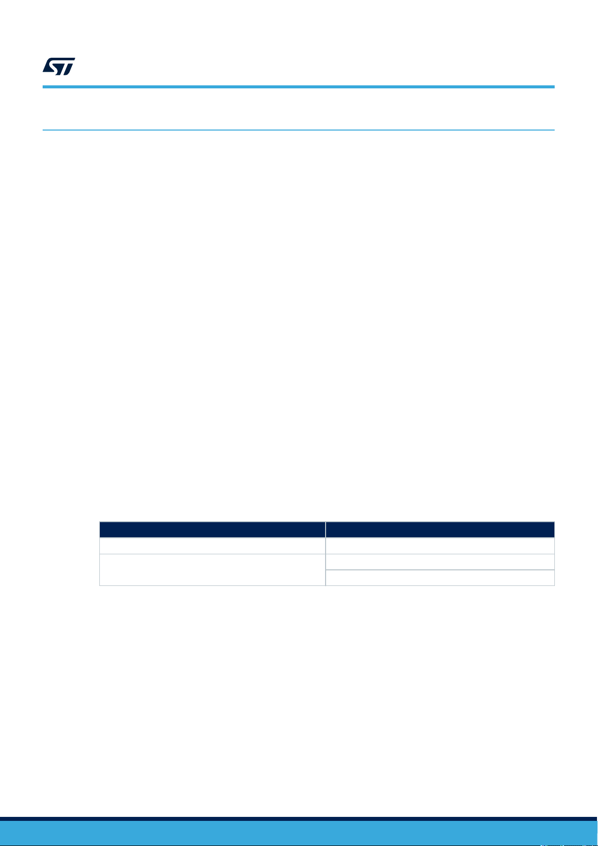
Contactless interface
UFDFPN5
1.7 x 1.4 mm
Wafer
Product status link
ST25TV02KC
ST25TV512C
• Compliant with ISO/IEC 15693
• NFC Forum Type 5 tag certified by the NFC Forum
• Supports all ISO/IEC 15693 modulations, coding, subcarrier modes, and
datarates up to 26 Kbit/s
• Single block reads and writes, multiple block reads
• Internal tuning capacitance: 23 pF
Memory
• Up to 2560 bits (320 bytes) of EEPROM
• Accessible by blocks of four bytes
• Write time from RF: typical 5 ms per block
• Data retention: 60 years at 55°C
• Minimum endurance: 100k write cycles
• 3-digit unique tap code
• Augmented NDEF (contextual automatic NDEF message)
Data protection
• User memory configurable in one or two areas:
– in single area mode, access protectable by one 64-bit password
– in flexible dual area mode, access protectable by two 32-bit passwords
• System configuration: access protected by a 32-bit password
• Permanent write lock of specific user area blocks
• Temporary write lock at user area level
• Permanent write lock of specific system configuration blocks
Product identification and protection
• Password features: cover coding, recovery, failed attempt counter
• Tamper detection capability with memorization of open/resealed events
• TruST25 digital signature
Privacy
• Configurable kill mode for permanent deactivation of the tag
• Untraceable mode with configurable responsiveness
Temperature range
• From - 40 to 85 °C
DS13304 - Rev 3 - April 2021
For further information contact your local STMicroelectronics sales office.
www.st.com

ST25TV02KC ST25TV512C
Package
• 5-pin package, ECOPACK2 (RoHS compliant)
• Bumped and sawn wafer
DS13304 - Rev 3
page 2/87
1 Description
The ST25TV02KC and ST25TV512C devices are NFC/RFID tag ICs with an Augmented NDEF feature, a tamper
detection interface, and specific modes to protect customer privacy.
The Augmented NDEF feature is a contextual automatic NDEF message service, allowing the tag to respond
dynamic content without an explicit update of the EEPROM by the end-user.
The tamper detection interface is available on ST25TV02KC-T devices only. This interface is not available on
ST25TV02KC‑A and ST25TV512C devices.
The ST25TV02KC and ST25TV512C devices hold a digital signature generated by TruST25 (a set of software
and procedures) to prove the origin of the chip in cloning detection, embeds a configurable EEPROM with 60-year
data retention, and can be operated from a 13.56 MHz long range RFID reader or an NFC phone.
The contactless interface is compliant with the ISO/IEC 15693 standard and NFC Forum Type 5 tag specification.
1.1 Block diagram
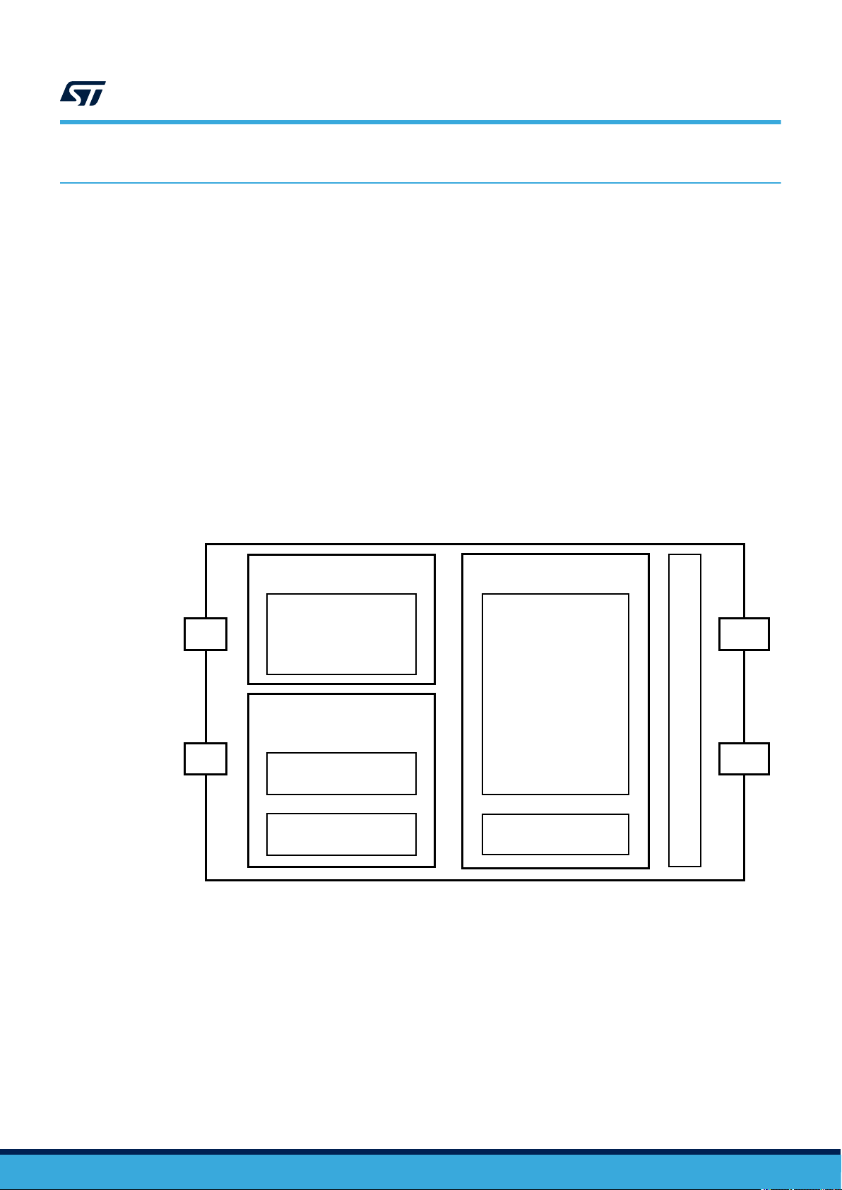
The ST25TV02KC and ST25TV512C (hereinafter referred to as ST25TVxxxC) devices are depicted in the
following block diagram:
ST25TV02KC ST25TV512C
Description
Figure 1. ST25TVxxxC block diagram
ANALOG FRONT END
EEPROM
RF interface
AC0
23 pF tuning
capacitance
User memory
(2)
DIGITAL CONTROL
UNIT
AC1
ISO/IEC 15693
protocol and control
Memory control
System registers
1. The tamper detection interface is available on ST25TV02KC-T devices only.
2. Respectively 512 and 2560 bits on ST25TV512C and ST25TV02KC devices.
(1)
TD0
TD1
TAMPER DETECTION
1.2 Package connections
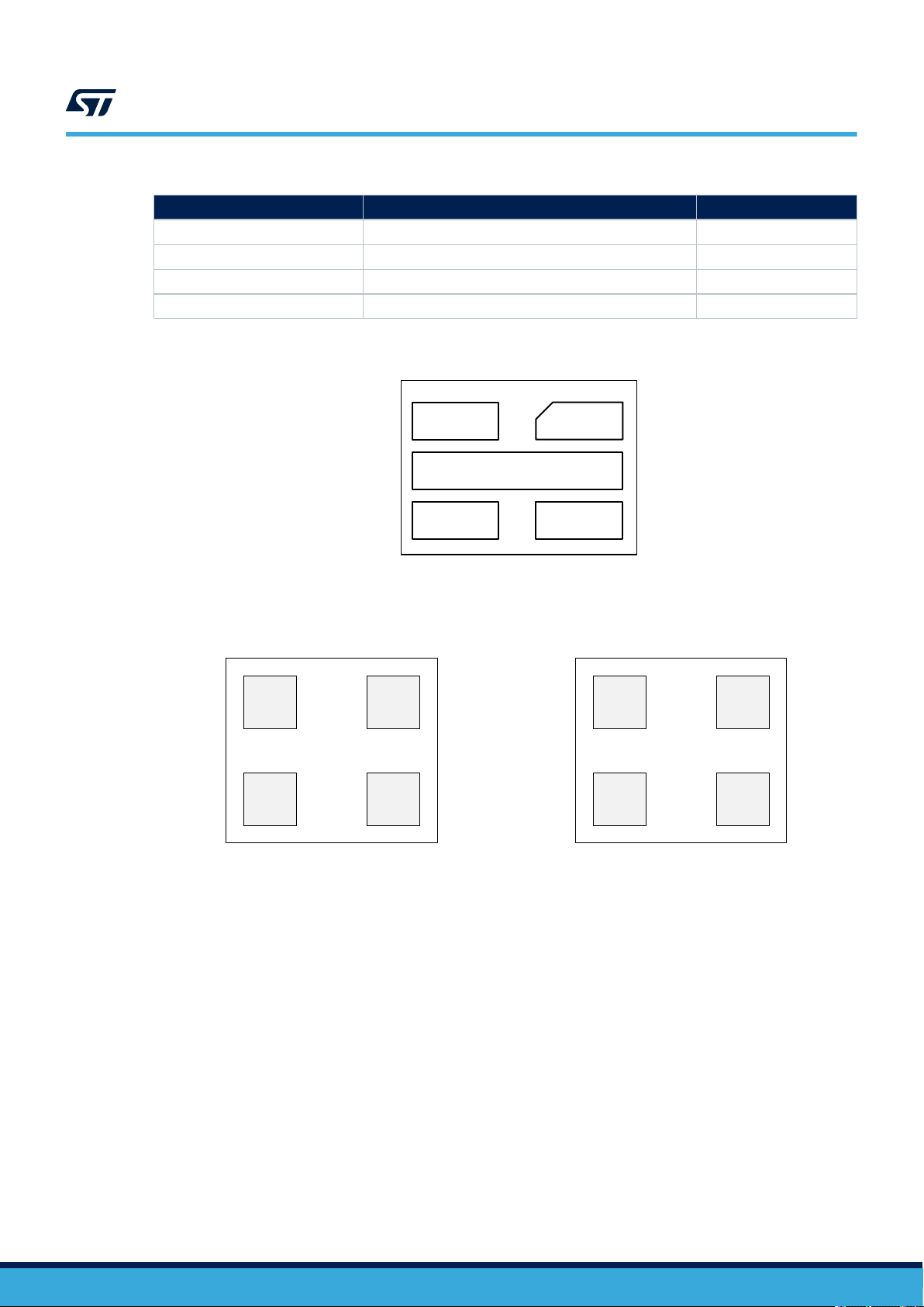
ST25TV02KC and ST25TV512C are provided in two delivery forms:
• UFDFPN5 package (ST25TV02KC-T devices only)
• Sawn and bumped wafer (ST25TV512C, ST25TV02KC-A and ST25TV02KC-T devices)
DS13304 - Rev 3
page 3/87
ST25TV02KC ST25TV512C
Package connections
Table 1. Signal names
Signal name Function Direction
AC0 Antenna coils In-out
AC1 Antenna coils In-out
TD0 Tamper detection loop In
TD1 Tamper detection loop Out
Figure 2. UFDFPN5 package connections
TD1
5 1
NC
AC1
4
UFDFPN5 pads side
Figure 3. Die connections for sawn and bumped wafer
AC0 NC
ST25TVxxxC-A
AC1 NC
Bumped pads side
TD0
2
NC
3
AC0
AC0 TD0
ST25TV02KC-T
AC1 TD1
Bumped pads side
DS13304 - Rev 3
page 4/87

2 Signal descriptions
2.1 Antenna coil (AC0, AC1)
These inputs are used to connect the ST25TVxxxC device to an external coil exclusively. It is advised not to
connect any other DC or AC path to AC0 or AC1.
When correctly tuned, the coil is used to power and access the device using the ISO/IEC 15693 and ISO 18000-3
mode 1 protocols.
2.2 Tamper detection (TD0, TD1)
These inputs are used to connect a wire loop to the ST25TVxxxC device to detect an open or a short between the
TD0 and TD1 pins.
ST25TV02KC ST25TV512C
Signal descriptions
DS13304 - Rev 3
page 5/87
3 Power management
The ST25TVxxxC device is powered through its contactless interface.
3.1 Device set
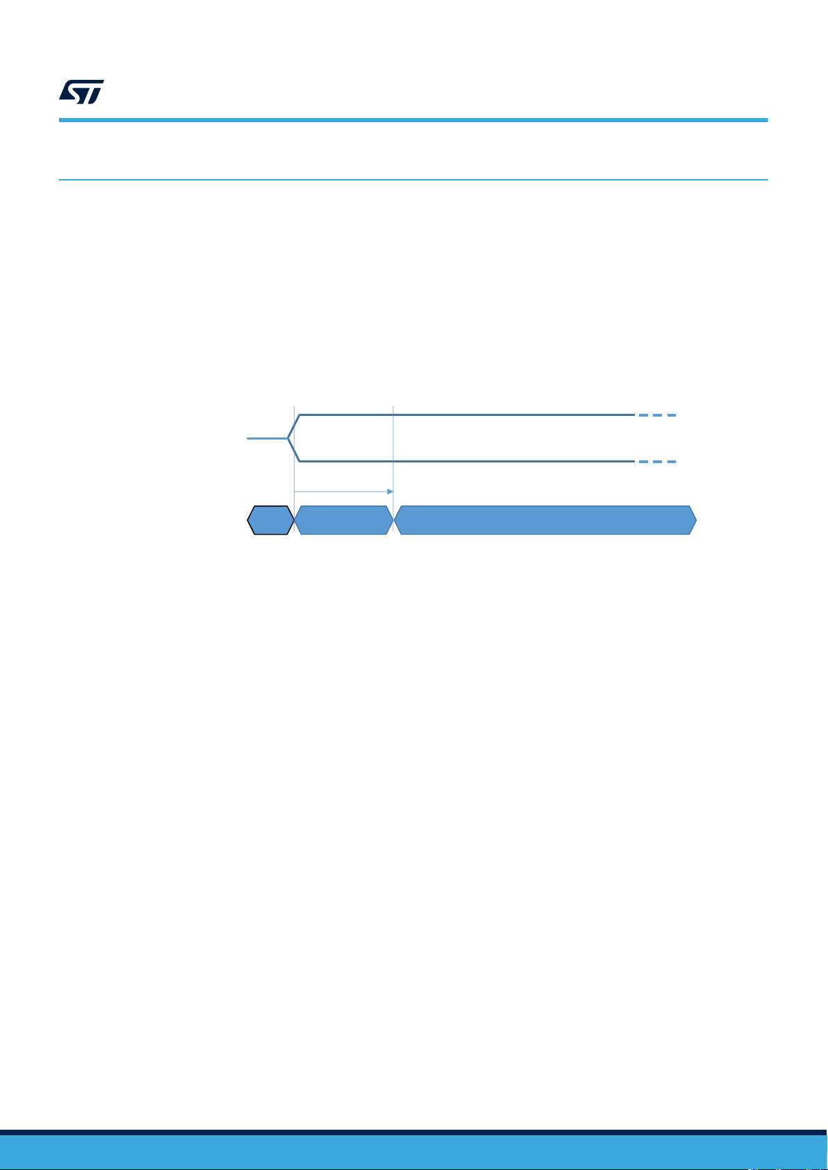
To ensure a proper boot of the RF circuitry, the RF field must be turned ON without any modulation for a
minimum period of time t
all received RF commands (see Figure 4).
RF Field:
BOOT_RF
(see Table 172. RF characteristics). During t
Figure 4. RF power-up sequence
t
BOOT_RF
ST25TV02KC ST25TV512C
Power management
BOOT_RF
, the ST25TVxxxC ignores
RF State:
3.2 Device reset
To ensure a proper reset of the RF circuitry, the RF field must be turned off (100% modulation) for a minimum
t
amount of time (see Table 172. RF characteristics).
RF_OFF
OFF
Boot
No RF access
allowed
ON = RF interface ready
DS13304 - Rev 3
page 6/87
4 Memory management
4.1 Memory organization
The ST25TVxxxC memory is organized as follows:
• User memory: it can be configured in one or two different areas, as described in Section 4.2 User memory.
Those areas can be used for user data and NFC Forum Type 5 Capability Container (CC) if required.
• System configuration memory: it is composed of different registers, including the device configuration, the
ISO15693 AFI and DSFID registers. It also contains the UID and different protection registers. Refer to
Section 4.3 System configuration memory for more details
ST25TV02KC ST25TV512C
Memory management
Figure 5. Memory organization
User memory
(3)
CC File
AREA1
(single area)
(1)
AREA1
(dual area)
AREA2
(dual area)
(2)
(2)
DS13304 - Rev 3
System
CFG
configuration
memory
1. NFC Forum T5T CC file is coded on block 00h which is part of AREA1.
2. In dual area mode, the AREA1/AREA2 boundary can be configured with a block granularity.
3. Respectively 16 and 80 blocks of 32 bits for ST25TV512C and ST25TV02KC devices.
SYS
page 7/87
4.2 User memory
User memory is addressed as blocks (= pages) of 4 bytes, starting at address 0 and ending at address
END_MEM. Value of END_MEM is 0Fh and 4Fh for ST25TV512C and ST25TV02KC devices respectively. The
ST25TVxxxC user memory can be configured in single area (AREA1) or in dual area mode (AREA1 and AREA2)
depending on the value of the END_A1 register at the start of a RF session (see Table 2. User memory in single
area mode, Table 3. User memory in dual area mode and Table 13. END_A1 content).
When the value of END_A1 is equal to END_MEM, the ST25TVxxxC user memory is configured in single area
mode defined as follows:
• AREA1 starts at address 00h. It is composed of (END_MEM+1) blocks. It can be read- or readwriteprotected by a dedicated 64-bit password. AREA1 is dedicated to user data.
When the value of END_A1 is lower than END_MEM, the ST25TVxxxC user memory is configured in dual area
mode defined as follows :
• AREA1 starts at address 00h. It is composed of (END_A1+1) blocks. It can be read- or readwrite-protected
by a dedicated 32-bit password. AREA1 is dedicated to user data.
• AREA2 starts at address (END_A1+1). It is composed of (END_MEM-END_A1) blocks. It can be read- or
readwrite-protected by a dedicated 32-bit password. AREA2 is dedicated to user data.
Block 00h belongs to AREA1, but can always be read regardless of the read-protection mode of AREA1. This
block is dedicated to the CC file content defined by the NFC Forum Type 5 application. An application that does
not need to comply with NFC Forum Type 5 specifications can use block 00h for any purpose.
ST25TV02KC ST25TV512C
User memory
Table 2. User memory in single area mode
RF command
ReadSingleBlock
ReadMultipleBlocks
WriteSingleBlock
Block
address
(1)
00h
LSByte - - MSByte
0000h 0001h 0002h 0003h
01h 0004h 0005h 0006h 0007h
02h 0008h 0009h 000Ah 000Bh
... ... ... ... ...
END_MEM END_MEM*4+0 END_MEM*4+1 END_MEM*4+2 END_MEM*4+3
1. Block 00h is always readable
2. For single area mode, set the value of END_A1 register to END_MEM
Byte address
Table 3. User memory in dual area mode
RF command
Block
address
(1)
00h
LSByte - - MSByte
0000h 0001h 0002h 0003h
01h 0004h 0005h 0006h 0007h
02h 0008h 0009h 000Ah 000Bh
ReadSingleBlock
ReadMultipleBlocks
WriteSingleBlock
... ... ... ... ...
END_A1 END_A1*4+0 END_A1*4+1 END_A1*4+2 END_A1*4+3
END_A1+1 END_A1*4+4 END_A1*4+5 END_A1*4+6 END_A1*4+7
... ... ... ... ...
END_MEM END_MEM*4+0 END_MEM*4+1 END_MEM*4+2 END_MEM*4+3
1. Block 00h is always readable
2. For dual area mode, set value of END_A1 register between 00h and (END_MEM-1)
Byte address
Comment
(2)
AREA1
Comment
(2)
AREA1
(2)
AREA2
DS13304 - Rev 3
page 8/87
4.3 System configuration memory
In addition to user memory, ST25TVxxxC includes a set of registers located in the system configuration memory.
Registers are read during the boot sequence and define basic ST25TVxxxC behaviour.
4.3.1 System configuration registers
Table 4. List of configuration registers lists the configuration registers of the ST25TVxxxC device. They are
accessed with the ReadConfiguration and WriteConfiguration commands and two arguments FID and PID,
respectively acting as a feature identifier and a parameter identifier.
The write access to the configuration registers is protected by the CONFIG security session which is opened by a
successful presentation of the PWD_CFG password (see Section 5.1.2 Password management).
Configuration registers are grouped by FID value. The write access to a group of registers may be permanently
locked.
Depending on the configuration register, its read access is either always granted or protected with the same
mechanisms as its write access.
Depending on the configuration register, when its content is updated during a RF session, the effect of the new
value is activated either immediately or at the start of the next RF session.
Table 4. List of configuration registers
Name
RW_PROTECTION_A1 00h 00h 1 Y W B Section 5.1.1
END_A1 00h 01h 1 Y W' B Section 5.1.1
RW_PROTECTION_A2 01h 00h 1 Y W B Section 5.1.1
UTC_EN 02h 00h 1 Y W B Section 5.2.1
UTC 02h 01h 3 Y N - Section 5.2.1
TD_EVENT_UPDATE_EN
TD_SEAL_MSG
TD_UNSEAL_MSG
TD_RESEAL_MSG
TD_SHORT_MSG
TD_OPEN_MSG
TD_STATUS
(4)
(4)
(4)
(4)
(4)
(4)
ANDEF_EN 04h 00h 1 Y W B Section 5.4.1
ANDEF_CFG 04h 01h 2 Y W B Section 5.4.1
ANDEF_SEP 04h 02h 1 R W I Section 5.4.1
ANDEF_CUSTOM_LSB 04h 03h 4 R W I Section 5.4.1
ANDEF_CUSTOM_MSB 04h 04h 4 R W I Section 5.4.1
PRIVACY 05h 00h 1 Y W B Section 5.5.1
AFI_PROT 08h 00h 1 Y W B Section 5.7.1
REV FEh 00h 1 Y N - Section 5.9
UID FEh 01h 8 Y N - Section 5.9
LCK_CONFIG FFh 00h 2 Y W'' I Section 5.1.1
1. Y: read access not protected, R: read access granted if LCK_CONFIG[FID]=0b and CONFIG security session open
2. N: write access not available, W: write access granted if LCK_CONFIG[FID]=0b and CONFIG security session open, W':
write access granted if LCK_CONFIG[1:0]=00b and CONFIG security session open, W'': write access granted if CONFIG
security session open
3. B: update is effective on next RF boot sequence, I: update is effective immediately
FID PID Bytes
(4)
03h 00h 1 Y W B Section 5.3.1
03h 01h 2 R W I Section 5.3.1
03h 02h 2 R W I Section 5.3.1
03h 03h 2 R W I Section 5.3.1
03h 04h 1 R W I Section 5.3.1
03h 05h 1 R W I Section 5.3.1
03h 06h 3 Y N - Section 5.3.1
Read
ST25TV02KC ST25TV512C
System configuration memory
(1)
Write
(2)
Activation time
(3)
Section
DS13304 - Rev 3
page 9/87
4. Registers with FID=03h are available only on ST25TV02KC-T devices (see section 10)
4.3.2 System registers
Table 5 lists the system registers of the ST25TVxxxC device. They are accessed with other RF commands than
ReadConfiguration and WriteConfiguration.
When the write access to a system register is available, it may be protected by a password and/or a lock
mechanism.
When the read access to a system register is available, it is always granted through the relevant RF command.
When the content of a system register is updated, the effect of the new value is activated immediately.
Name Bytes
LCK_BLOCK 10 R W I Section 5.1.1
LCK_DSFID 1 N W I Section 5.9
LCK_AFI 1 N W I Section 5.9
DSFID 1 Y W I Section 5.9
AFI 1 Y W I Section 5.9
IC_REF 1 Y N - Section 5.9
UID 8 Y N - Section 5.9
ANDEF_UID 16 Y N - Section 5.4.1
KILL_CMD 1 N W I Section 5.5.1
UNTR_CMD 1 N W I Section 5.5.1
RND_NUMBER 2 Y
PWD_CFG 4 N W I Section 5.1.1
PWD_A1 4 N W I Section 5.1.1
PWD_A2 4 N W I Section 5.1.1
PWD_UNTR 4 N W I Section 5.1.1
1. Y: read access granted without condition, R: read access granted with condition
2. N: write access not available, W: write access granted with condition
3. The content of the RND_NUMBER register is updated internally on a successful GetRandomNumber request
Table 5. List of system registers
Read
(1)
Write
N
(2)
(3)
Activation time Section
ST25TV02KC ST25TV512C
System configuration memory
- Section 5.1.1
DS13304 - Rev 3
page 10/87
5 Specific features
ST25TVxxxC offers the following features:
• Section 5.1 Data protection
• Section 5.2 Unique tap code
• Section 5.3 Tamper detection
• Section 5.4 Augmented NDEF
• Section 5.5 Consumer privacy protection
• Section 5.6 TruST25 digital signature
• Section 5.7 AFI protection
• Section 5.8 Inventory Initiated
The features from Section 5.1 to Section 5.7 can be programmed by accessing registers of the ST25TVxxxC
using the ReadConfiguration and WriteConfiguration commands. Update of configuration registers is only possible
when the access right has been granted by presenting the configuration password (PWD_CFG), and if the
configuration of the feature was not previously locked (see register LCK_CONFIG).
Depending on the configuration register, the effect of a valid write access may be applied immediately or during
the boot sequence of the next RF session.
An additional set of registers allows to identify and customize the product (see Section 5.9 Device identification
registers.).
ST25TV02KC ST25TV512C
Specific features
5.1 Data protection
ST25TVxxxC provides a special data protection mechanism based on passwords that unlock security sessions.
Read and/or write access to the user memory can be protected. Write access to the configuration registers is
always protected. Read access to some configuration registers is protected.
Other lock mechanisms are supported (LockBlock, lock by feature), as described in this section.
5.1.1 Data protection registers
RF Command Access type
ReadConfiguration @(FID=FFh, PID=00h) R : always possible
WriteConfiguration @(FID=FFh, PID=00h)
Table 6. LCK_CONFIG access
W : if the CONFIG security session is open
W effective time : immediate
DS13304 - Rev 3
page 11/87
ST25TV02KC ST25TV512C
Data protection
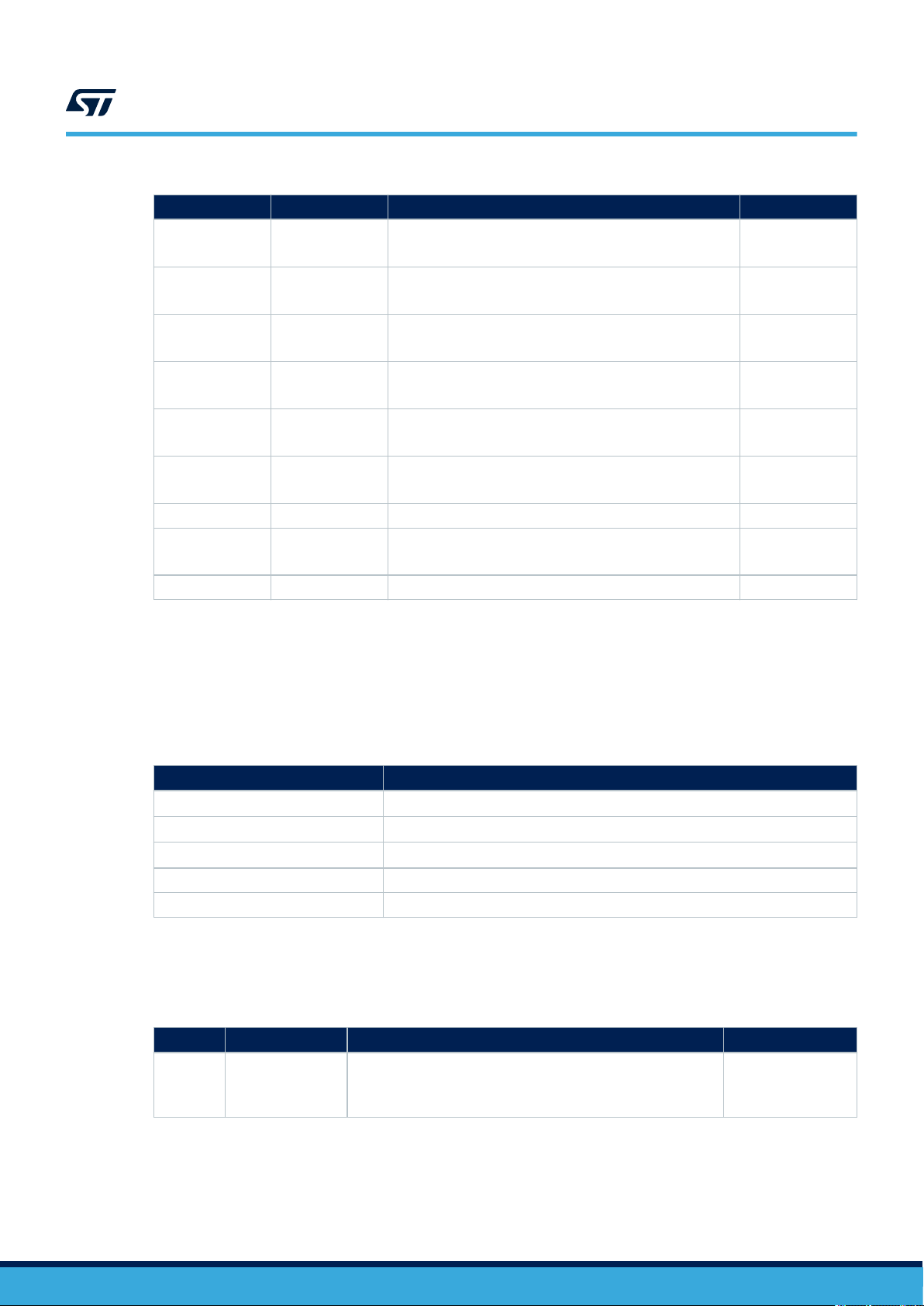
Table 7. LCK_CONFIG content
Bit Name Function Factory value
b0 LCK_A1
b1 LCK_A2
b2 LCK_UTC
b3 LCK_TD
b4 LCK_ANDEF
b5 LCK_PRIV
b7-b6 RFU - 00b
b8 LCK_AFIP
b15-b9 RFU - 0000000b
0: configuration registers with FID=00h are not locked
1: configuration registers with FID=00h are locked
0: configuration registers with FID=01h are not locked
1: configuration registers with FID=01h are locked
0: configuration registers with FID=02h are not locked
1: configuration registers with FID=02h are locked
0: configuration registers with FID=03h are not locked
1: configuration registers with FID=03h are locked
0: configuration registers with FID=04h are not locked
1: configuration registers with FID=04h are locked
0: configuration registers with FID=05h are not locked
1: configuration registers with FID=05h are locked
0: configuration registers with FID=08h are not locked
1: configuration registers with FID=08h are locked
0b
0b
0b
0b
0b
0b
0b
Note: Refer to Table 4. List of configuration registers for the LCK_CONFIG register.
If value 1b is issued for a field already set to 1b, the WriteConfiguration command has no effect and error 11h
shall be responded.
Otherwise, if value 0b is issued for a field set to 1b, the corresponding feature remains locked and no errorcode is
responded to the WriteConfiguration command.
Table 8. LCK_BLOCK access
RF Command
ReadSingleBlock
ReadMultipleBlocks
GetMultipleBlockSecurityStatus
R : if Option_flag=1 and write access to parent area is allowed
R : if Option_flag=1 and write access to parent area is allowed
R : if write access to parent area is allowed
LockBlock W : if not already locked and write access to parent area is allowed
- W effective time : immediate
1. When the write access to an area is not allowed (write access forbidden, or protected with closed security session),
then the value of LCK_BLOCK is masked by 1 in a BSS field (see sections Section 6.4.3 ReadSingleBlock,
Section 6.4.6 ReadMultipleBlocks and Section 6.4.14 GetMultipleBlockSecurityStatus)
Access type
Table 9. LCK_BLOCK content
Bit
b79-b0 LCK_BLOCK
Name Function Factory Value
For each bit bN:
• 0: write access of block N not locked
• 1: write access of block N permanently
(1)
(1)
(1)
0
Note: Refer to Table 5. List of system registers for the LCK_BLOCK register.
DS13304 - Rev 3
page 12/87
ST25TV02KC ST25TV512C
Data protection
Table 10. RW_PROTECTION_A1 access
RF Command Type
ReadConfiguration @(FID=00h, PID=00h) R : always possible
WriteConfiguration @(FID=00h, PID=00h)
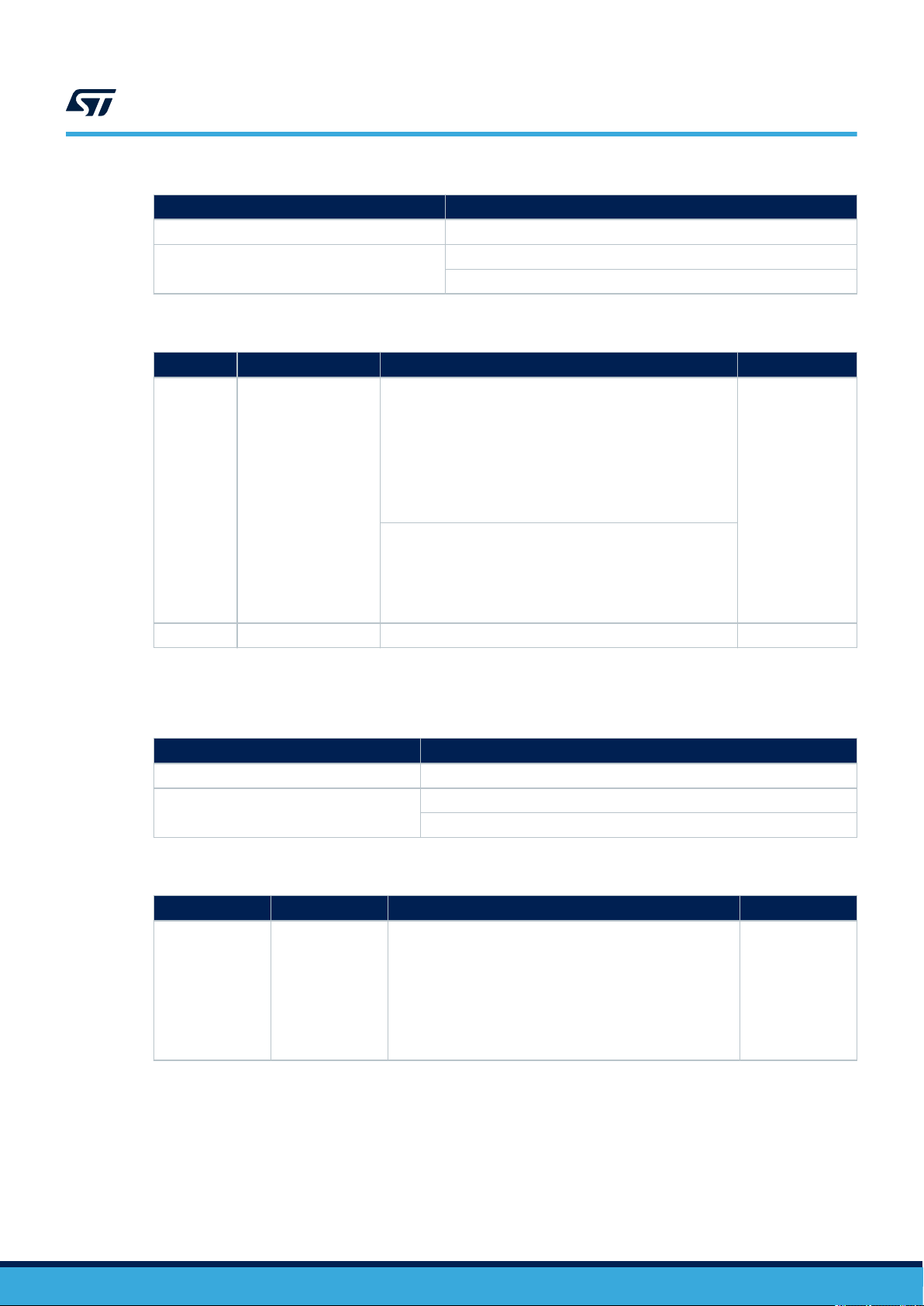
Table 11. RW_PROTECTION_A1 content
Bit Name Function Factory Value
AREA1 access rights (except block 00h):
• 00: read always allowed / write always allowed
• 01: read always allowed / write allowed if AREA1 security
• 10: read allowed if AREA1 security session is open /
b1-b0 RW_PROTECTION_A1
b7-b2 RFU - 000000b
• 11: read allowed if AREA1 security session is open /
Block 00h access rights: read always allowed
• 00: write always allowed
• 01: write allowed if AREA1 security session is open
• 10: write allowed if AREA1 security session is open
• 11: write forbidden
W : if the CONFIG security session is open and LCK_A1=0b
W effective time : on next RF boot sequence
session is open
write allowed if AREA1 security session is open
write forbidden
00b
Note: Refer to Table 4. List of configuration registers for the RW_PROTECTION_A1 register.
Table 12. END_A1 access
RF command
ReadConfiguration @(FID=00h, PID=01h) R : always possible
WriteConfiguration @(FID=00h, PID=01h)
W : if the CONFIG security session is open and LCK_A1=LCK_A2=0b
W effective time : on next RF boot sequence
Access type
Table 13. END_A1 content
Bit
b7-b0 END_A1
1. END_MEM value is 0Fh / 4Fh for ST25TV512C / ST25TV02KC devices respectively.
Name Function Factory Value
Number of the last block belonging to AREA1.
When lower than END_MEM, user memory is split in two
areas :
• AREA1 (blocks 00h to END_A1)
• AREA2 (blocks END_A1 + 1 to END_MEM).
Otherwise user memory contains a single area : AREA1
(blocks 00h to END_MEM)
Note: Refer to Table 4. List of configuration registers for the END_A1 register.
END_MEM
(1)
DS13304 - Rev 3
page 13/87
ST25TV02KC ST25TV512C
Data protection
Table 14. RW_PROTECTION_A2 access
RF command Access type
ReadConfiguration @(FID=01h, PID=00h) R : always possible
WriteConfiguration @(FID=01h, PID=00h)
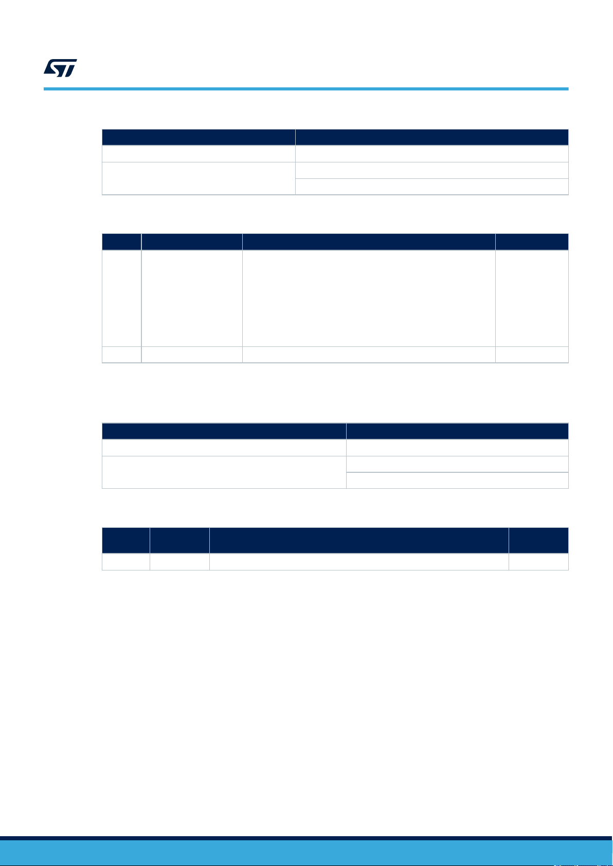
Table 15. RW_PROTECTION_A2 content
Bit Name Function Factory Value
AREA2 access rights:
• 00: read always allowed / write always allowed
• 01: read always allowed / write allowed if AREA2 security
b1-b0 RW_PROTECTION_A2
b7-b2 RFU - 000000b
session is open
• 10: read allowed if AREA2 security session is open / write
allowed if AREA2 security session is open
• 11: read allowed if AREA2 security session is open / write not
allowed
W : if the CONFIG security session is open and LCK_A2=0b
W effective time : on next RF boot sequence
00b
Note: Refer to Table 4. List of configuration registers for the RW_PROTECTION_A2 register.
Table 16. PWD_CFG access
RF command
- R: no read access
WritePassword @PID=00h
W: if the CONFIG security session is open
W effective time: immediate
Access type
Table 17. PWD_CFG content
Bit Name Function
b31-b0 PWD_CFG Password for access to configuration registers and Kill command 00000000h
Note: Refer to Table 5. List of system registers for the PWD_CFG register.
Factory
Value
DS13304 - Rev 3
page 14/87
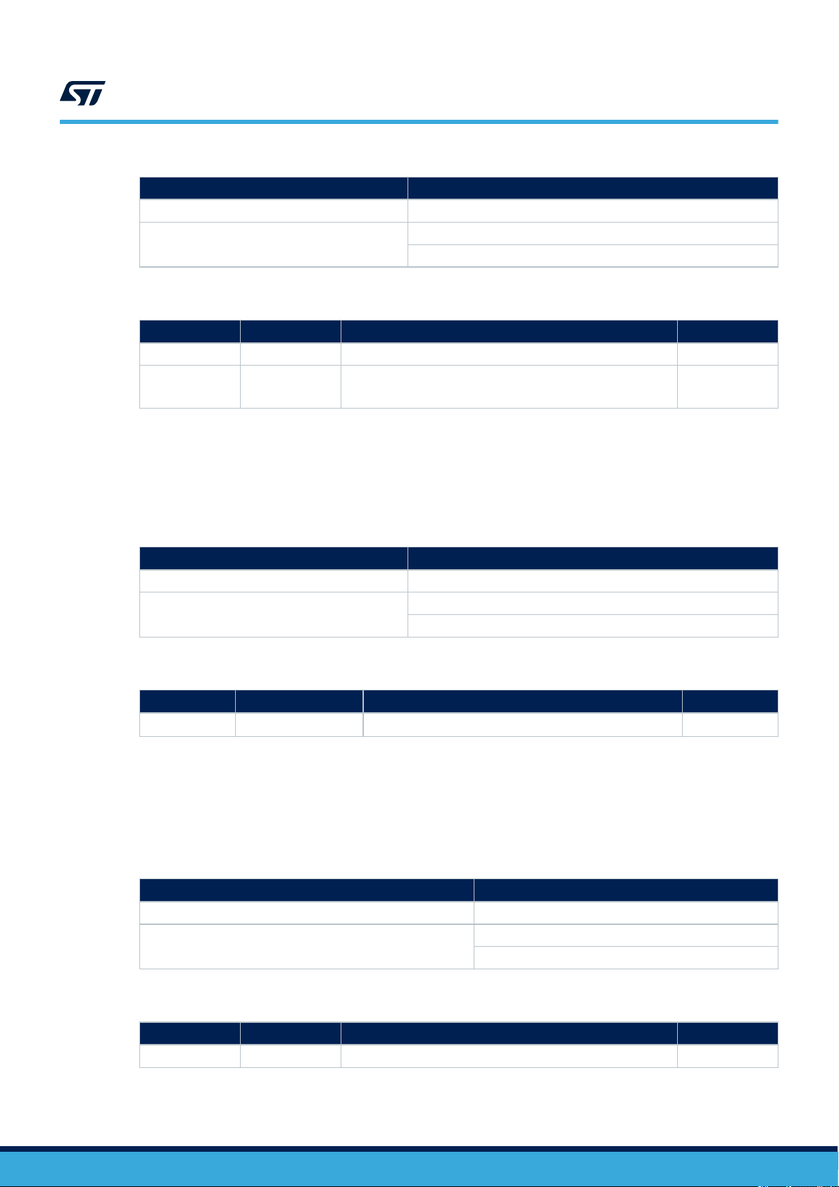
Table 18. PWD_A1 access
RF command Access type
- R : no read access
WritePassword @PID=01h
W : if AREA1 security session is open
W effective time : immediate
Table 19. PWD_A1 content
Bit Name Function Factory Value
b31-b0 PWD_A1_LSB Password for access to AREA1 00000000h
In single area mode, bits 0 to 63 are used.
(1)
In dual area mode only bits 0 to 31 are used
b63-b32
PWD_A1_MSB
1. PWD_A1_MSB is an alias of register PWD_A2:
• when switching from dual to single area mode, the value of PWD_A1_MSB is the latest known value of PWD_A2
• when switching from single to dual area mode, the value of PWD_A2 is the latest known value of PWD_A1_MSB
Note: Refer to Table 5. List of system registers for the PWD_A1 register.
ST25TV02KC ST25TV512C
Data protection
00000000h
Table 20. PWD_A2 access
RF command
- R : no read access
WritePassword @PID=02h
W : if AREA2 security session is open
W effective time : immediate
Table 21. PWD_A2 content
Bit
b31-b0
1. PWD_A1_MSB is an alias of register PWD_A2:
• when switching from dual to single area mode, the value of PWD_A1_MSB is the latest known value of PWD_A2
• when switching from single to dual area mode, the value of PWD_A2 is the latest known value of PWD_A1_MSB
Name Function Factory Value
PWD_A2
(1)
Password for access to AREA2 00000000h
Note: Refer to Table 5. List of system registers for the PWD_A2 register.
Table 22. PWD_UNTR access
RF command
- R : no read access
WritePassword @PID=03h
W : if UNTR security session is open
W effective time : immediate
Access type
Access type
Table 23. PWD_UNTR content
Bit
b31-b0 PWD_UNTR Password used with ToggleUntraceable command 00000000h
Name Function Factory Value
Note: Refer to Table 5. List of system registers for the PWD_UNTR register.
DS13304 - Rev 3
page 15/87
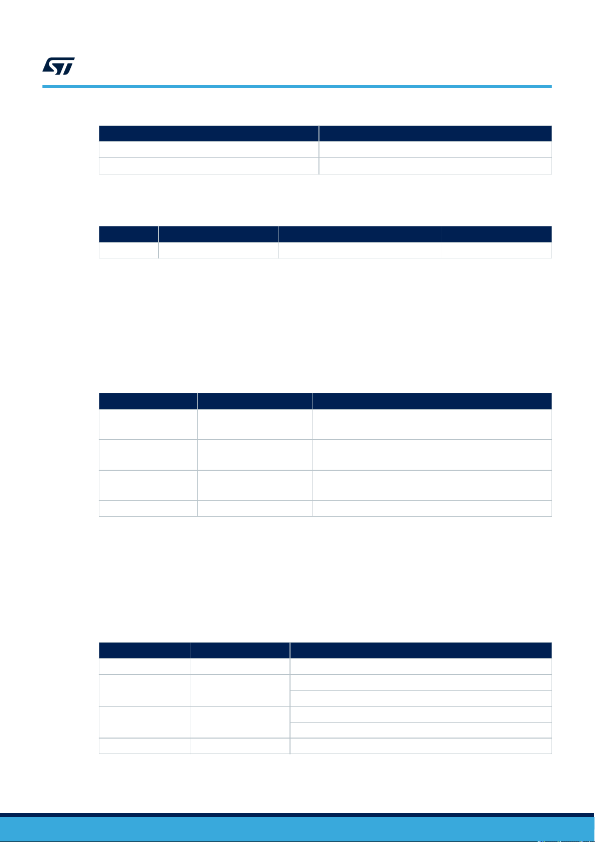
Table 24. RND_NUMBER access
RF command Access type
GetRandomNumber R : always possible
1. the content of the RND_NUMBER register is updated internally on a successful GetRandomNumber command.
-
W : no write access
Table 25. RND_NUMBER content
Bit Name Function Factory value
b15-b0 RND_NUMBER 16-bit random number N/A
Note: Refer to Table 5. List of system registers for the RND_NUMBER register.
5.1.2 Password management
ST25TVxxxC provides protection of user and system configuration memories. Access to groups of data are
controlled by security sessions based on passwords. On successful (respectively failed) presentation of a
password, a security session is open (respectively closed) and grants (respectively denies) access to the
protected group of data.
ST25TV02KC ST25TV512C
Data protection
(1)
Table 26. Security session type
Security session Open by presenting Rights granted when session is open
CONFIG PWD_CFG
AREA1 PWD_A1
AREA2 PWD_A2
UNTR PWD_UNTR Update of PWD_UNTR
Access to configuration registers
Update of PWD_CFG
Access to blocks from AREA1 in user memory
Update of PWD_A1
Access to blocks from AREA2 in user memory
Update of PWD_A2
Each of the PWD_CFG and PWD_UNTR passwords is 32-bit long.
In dual area mode (END_A1 < END_MEM), each of the PWD_A1 and PWD_A2 passwords is 32-bit long.
In single area mode (END_A1 = END_MEM), the PWD_A1 password is 64-bit long, and AREA2 security session
is not applicable: password commands fail with password identifier 02h when single area mode is used.
Note: In addition to the security session mechanism described in this section, the PWD_CFG and PWD_UNTR
passwords are respectively used with the Kill and ToggleUntraceable commands.
Table 27. List of password registers
Password
PWD_CFG 00h 4 bytes
PWD_A1 01h
PWD_A2 02h
PWD_UNTR 03h 4 bytes
Password_id Password_data size
4 bytes if END_A1 < END_MEM
8 bytes if END_A1 = END_MEM
4 bytes if END_A1 < END_MEM
Invalid request if END_A1 = END_MEM
DS13304 - Rev 3
page 16/87

ST25TV02KC ST25TV512C
Data protection
The ST25TVxxxC passwords management is based on three commands:
• WritePassword (see Section 6.4.18 WritePassword)
• PresentPassword (see Section 6.4.19 PresentPassword)
• GetRandomNumber (see Section 6.4.24 GetRandomNumber)
For any of the 4x passwords available, three actions are possible:
• Open Security Session:
– Use GetRandomNumber command if needed
– Use PresentPassword command with corresponding password identifier and valid encrypted password
value (see Section 5.1.4 User memory protection)
• Update Password:
– While the security session for the corresponding password is open, use WritePassword command with
same password identifier and the new encrypted password value (see Section 5.1.4 User memory
protection).
• Close Security Session:
– To close the security session corresponding to a password identifier, user can choose one of the
following options:
◦ Remove tag from RF field
◦ Use PresentPassword command with same password identifier and an invalid password value
◦ Open a security session corresponding to a different password identifier. Opening a new security
session automatically closes the previously opened one (even if the open operation fails)
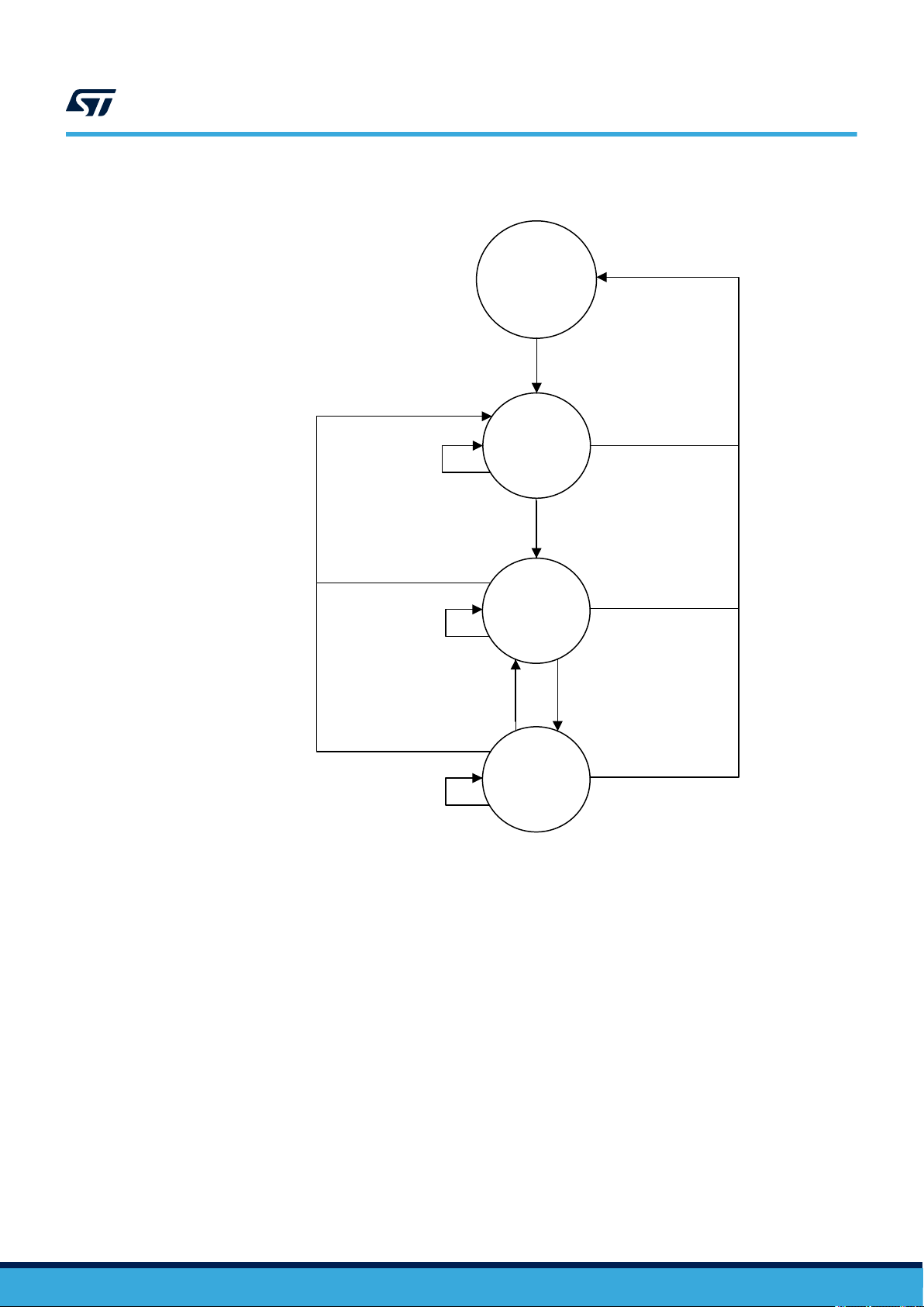
Figure 6 describes the mechanism to open/close the security sessions.
DS13304 - Rev 3
page 17/87
ST25TV02KC ST25TV512C
Figure 6. Security sessions management
ST25TVxxxC
out of RF field
Data protection
Present any
password not OK
Any other
command
Any other
command
PWD_x OK
Any other
command
Present
Field ON
All security
sessions
closed
PWD_x OK
Security
session x
opened
(y closed)
Security
session y
opened
(x closed)
Field OFF
Present
Present
PWD_y OK
DS13304 - Rev 3
Password recovery
The ST25TVxxxC devices provide a password recovery feature, which allows the user to reprogram a corrupted
password after a RF field failure during a WritePassword command.
Refer to “AN5577 - Password management for ST25TV512C and ST25TV02KC devices", for more details on how
to use it. Contact your STMicroelectronics sales office to get this document.
Password attempt limit
The ST25TVxxxC devices offer the capability to protect a password against brute-force attacks, thanks to a limiter
mechanism on failed password attempts.
Refer to “AN5577 - Password management for ST25TV512C and ST25TV02KC devices", for more details on how
to use it. Contact your STMicroelectronics sales office to get this document.
page 18/87
ST25TV02KC ST25TV512C
Data protection
5.1.3 Password encryption
An encryption mechanism - known as cover coding - is used to transmit coded password values in the
Password_data field of the following command frames:
• PresentPassword request (see Section 6.4.19 PresentPassword),
• WritePassword request (see Section 6.4.18 WritePassword)
• Kill request (see Section 6.4.20 Kill)
• ToggleUntraceable request (see Section 6.4.23 ToggleUntraceable)
The mechanism requires that a call to the GetRandomNumber command has been issued since the latest boot of
the ST25TVxxxC device, otherwise these password commands fail.
Additionally, if the latest call to a PresentPassword / Kill / ToggleUntraceable command failed because of an
invalid value of the Password_data field, it is required that a call to the GetRandomNumber command is issued
before attempting a new call to either of these three commands, otherwise their execution will fail regardless of
the new value of the Password_data field.
Note: If the latest execution of a PresentPassword / ToggleUntraceable command was successful, it is not necessary
to issue a new call to the GetRandomNumber command before issuing a new PresentPassword / Kill /
ToggleUntraceable request.
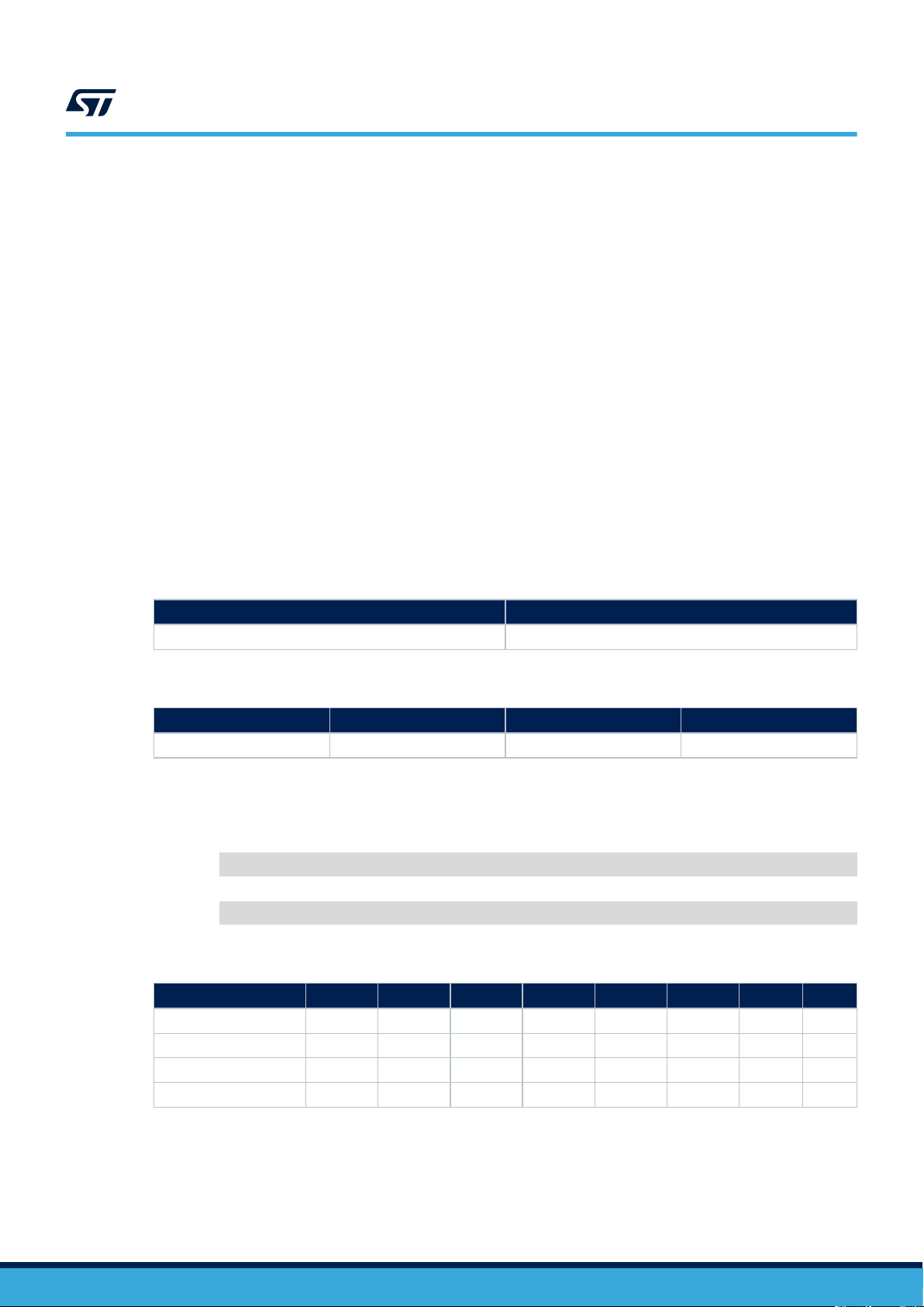
Assuming these constraints are fulfilled, let the RND_NUMBER_4B and RND_NUMBER_8B values be computed
from the concatenation of the RND_NUMBER register value returned by the latest call to the GetRandomNumber
request.
Table 28. RND_NUMBER_4B
b31-b16
RND_NUMBER RND_NUMBER
b15-b0
Table 29. RND_NUMBER_8B
b63-b48
RND_NUMBER RND_NUMBER RND_NUMBER RND_NUMBER
b47-b32 b31-b16 b15-b0
Let PASSWORD_4B (resp. PASSWORD_8B) be the unencrypted value of a 32-bit (resp. 64-bit) password to be
transmitted over a PresentPassword / WritePassword / Kill / ToggleUntraceable request.
The Password_data field in a request frame shall be computed as follows :
• for a 32-bit password :
Password_data = XOR(RND_NUMBER_4B , PASSWORD_4B)
–
• for a 64-bit password :
Password_data = XOR(RND_NUMBER_8B , PASSWORD_8B)
–
Table 30. Example of 64-bit Password_data value computation
Data name
RND_NUMBER - - - - - - 1Dh E6h
RND_NUMBER_8B 1Dh E6h 1Dh E6h 1Dh E6h 1Dh E6h
PASSWORD_8B FAh D7h 5Eh 15h CAh A5h D0h D4h
Password_data E7h 31h 43h F3h D7h 43h CDh 32h
b63-b56 b55-b48 b47-b40 b39-b32 b31-b24 b23-b16 b15-b8 b7-b0
Note: A field coded on several bytes – such as Password_data – is transmitted in LSB to MSB byte order in ISO15693
request and response frames
DS13304 - Rev 3
page 19/87
When processing a PresentPassword / Kill / ToggleUntraceable request, the ST25TVxxxC device decrypts the
Password_data field to obtain the unencrypted value PASSWORD_4B (or PASSWORD_8B), which is used for
comparison with the password register identified by the Password_id field.
When processing a WritePassword request, the ST25TVxxxC device decrypts the Password_data field to obtain
the unencrypted value PASSWORD_4B (or PASSWORD_8B) , which is used for update of the password register
identified by the Password_id field.
5.1.4 User memory protection
A read and/or write access protection can be globally applied to the blocks of an area. Such protection can be
individually configured for AREA1 and AREA2, thanks to the RW_PROTECTION_A1 and RW_PROTECTION_A2
registers (see Table 11. RW_PROTECTION_A1 content and Table 15. RW_PROTECTION_A2 content).
On factory delivery, access to AREA1 and AREA2 are not protected. When updating RW_PROTECTION_Ax
registers, the new protection mode is effective during the boot sequence of the next RF session.
In addition to the area protection mechanism, the write access to each block composing AREA1 and AREA2 can
be individually locked thanks to the LockBlock command.
Block 00h is an exception to the area protection mechanism:
• when block 00h is not locked, the protection of its write access is determined by the value of
RW_PROTECTION_A1 register, like other blocks of AREA1
• read access to block 00h is always allowed, regardless of the value of RW_PROTECTION_A1 register
The RW_PROTECTION_A1 register is locked when register LCK_A1 is set to 1b.
The RW_PROTECTION_A2 register is locked when register LCK_A2 is set to 1b.
The END_A1 register is locked when either of LCK_A1 and LCK_A2 registers is set to 1b.
ST25TV02KC ST25TV512C
Data protection
Retrieve the security status of a user memory block
User can read a block security status (BSS) by issuing following commands:
• GetMultipleBlockSecurityStatus
• ReadSingleBlock with Option_flag set to 1
• ReadMultipleBlocks with Option_flag set to 1
For each block, ST25TVxxxC will respond with a BSS byte containing a Lock_bit flag (b0 in Table 31) as specified
in ISO 15693 standard.
Table 31. Block security status
b7
b6 b5 b4 b3 b2 b1 b0
0: RFU
0: Write access to current block granted
1: Write access to current block denied
This Lock_bit flag is set to one if write access to the corresponding block is not allowed. This happens when either
of the following conditions is met:
• the write access to the block was permanently locked (corresponding bit of LCK_BLOCK register set to 1b)
by a successful LockBlock command
• write access to parent area is protected (RW_PROTECTION_Ax = 01b or 10b at start of the RF session)
and security session is closed
• write access to parent area is forbidden (RW_PROTECTION_Ax = 11b at start of the RF session)
5.1.5 System configuration memory protection
Configurations registers listed Table 4. List of configuration registers are accessed using the ReadConfiguration
and WriteConfiguration commands.
Configuration registers are grouped by feature. A group is identified by parameter FID, a register from this group
is identified by parameter PID.
Write access to configuration registers is protected or forbidden.
Note: Write access to read-only configuration registers is forbidden
DS13304 - Rev 3
page 20/87
ST25TV02KC ST25TV512C
Unique tap code
Protected write access to a configuration register is granted when the CONFIG security session is open, and its
parent group is not permanently locked.
Read access to configuration registers is protected or always allowed. Protected read access to a configuration
register is granted when the CONFIG security session is open, and its parent group is not permanently locked.
On factory delivery, configuration groups are not locked (all bits of LCK_CONFIG register are set to 0b). A
configuration group identified by FID (00h, 01h, 02h, 03h, 04h, 05h or 08h) can be permanently locked by setting
bit FID of LCK_CONFIG register to 1b:
• if the read access to a configuration register from this group was protected, the register can no longer be
read even if CONFIG security session is open
• if the write access to a configuration register from this group was protected, the register can no longer be
written even if CONFIG security session is open
• write access to LCK_CONFIG register (FID=FFh, PID=00h) is granted when the CONFIG security session is
open
• user cannot unlock a configuration group by setting bit FID of LCK_CONFIG back to 0b, even after opening
CONFIG security session (Lock is permanent)
• user may lock several configuration groups with a single WriteConfiguration command by setting the
respective bits of LCK_CONFIG to 1b in the request
System registers listed in Table 5. List of system registers include passwords, device identification registers, lock
status and command status.
Read access to system registers is available except for passwords, AFI and DSFID lock status , Kill and
ToggleUntraceable command status.
Device identification registers are detailed in section 5.10:
• Write access to AFI and DFSID registers can be respectively locked by LockAFI and LockDSFID
commands. Lock is permanent: once locked, write access to AFI and DSFID registers is forbidden.
• Other device identification registers (IC_REF, UID) are read only registers.
5.2
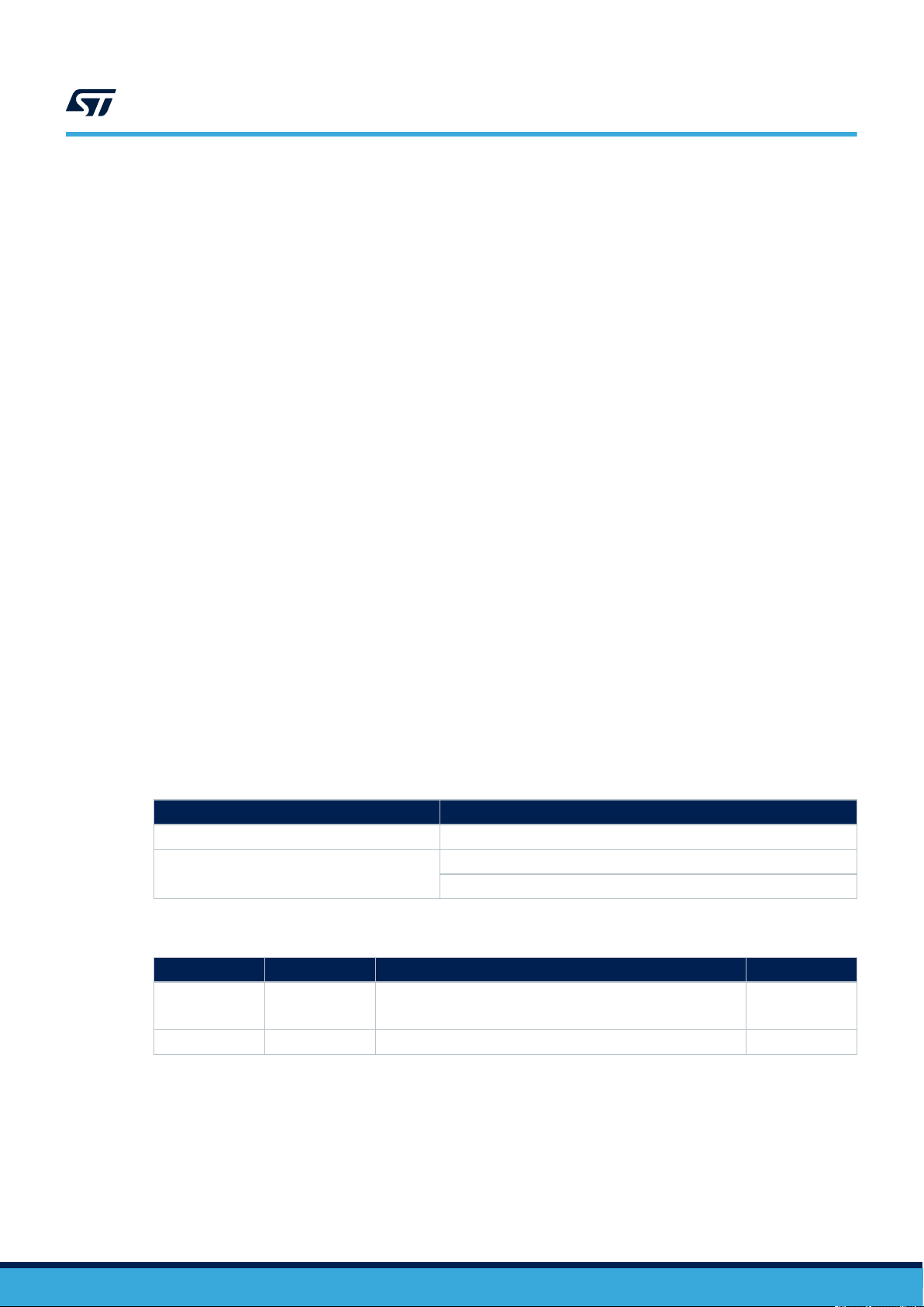
Unique tap code
5.2.1 Unique tap code registers
Table 32. UTC_EN access
RF command Access type
ReadConfiguration @(FID=02h, PID=00h) R : always possible
WriteConfiguration @(FID=02h, PID=00h)
Bit Name Function Factory value
b0 UTC_EN
b7-b1 RFU - 0000000b
0: Unique tap code is disabled
1: Unique tap code is enabled
Note: Refer to Table 4. List of configuration registers for the UTC_EN register.
W : if the CONFIG security session is open and LCK_UTC=0b
W effective time : on next RF boot sequence
Table 33. UTC_EN content
0b
DS13304 - Rev 3
page 21/87
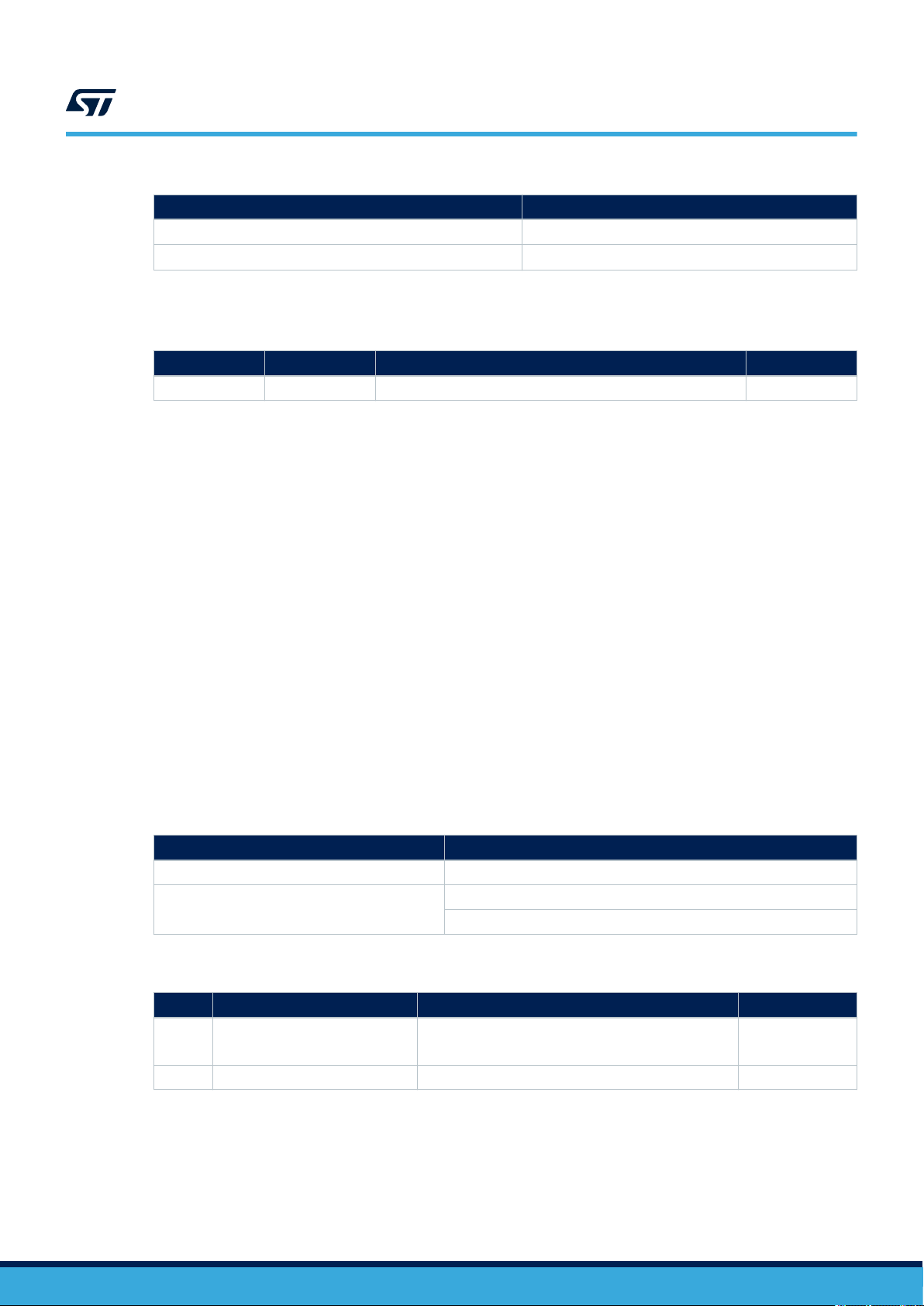
Table 34. UTC access
RF command Access type
ReadConfiguration @(FID=02h, PID=01h) R : always possible
1. the content of the UTC register is updated internally during the RF boot sequence when UTC_EN is set to 1b
-
W : no write access
Table 35. UTC content
Bit Name Function Factory value
b23-b0 UTC Unique tap code value Not applicable
Note: Refer to Table 4. List of configuration registers for the UTC register.
5.2.2 Unique tap code description
When the UTC_EN register is set to 1b, the content of the UTC register is updated internally with a fresh value
during each RF boot sequence. The content of the UTC register is coded in ASCII format.
The UTC_EN register is locked when register LCK_UTC is set to 1b.
Note: When the Unique tap code is enabled, the duration of the RF boot sequence t
• compliant with the 5ms guard-time value defined in the NFC Forum [DIGITAL] specification
• not compliant with the 1ms guard-time value defined in the ISO15693 specification
Refer to “AN5578 - Unique tap code for ST25TV512C and ST25TV02KC devices", for more details on the content
of the UTC register. Contact your STMicroelectronics sales office to get this document.
ST25TV02KC ST25TV512C
Tamper detection
(1)
(see section 8.2) is:
Boot_RF
5.3 Tamper detection
The tamper detection feature is available on ST25TV02KC-T devices only (see section 10). On ST25TVxxxC-A
devices, ReadConfiguration and WriteConfiguration commands requested with FID=03h fail with error code 10h.
5.3.1 Tamper detection registers
Table 36. TD_EVENT_UPDATE_EN access
RF command Access type
ReadConfiguration @(FID=03h, PID=00h) R : always possible
WriteConfiguration @(FID=03h, PID=00h)
Table 37. TD_EVENT_UPDATE_EN content
Bit Name Function Factory value
b0 TD_EVENT_UPDATE_EN
b7- b1 RFU - 0000000b
Note: Refer to Table 4. List of configuration registers for the TD_EVENT_UPDATE_EN register.
W : if the CONFIG security session is open and LCK_TD=0b
W effective time : on next RF boot sequence
0: memorization of tamper events disabled
1: memorization of tamper events enabled
0b
DS13304 - Rev 3
page 22/87
ST25TV02KC ST25TV512C
Tamper detection
Table 38. TD_SEAL_MSG access
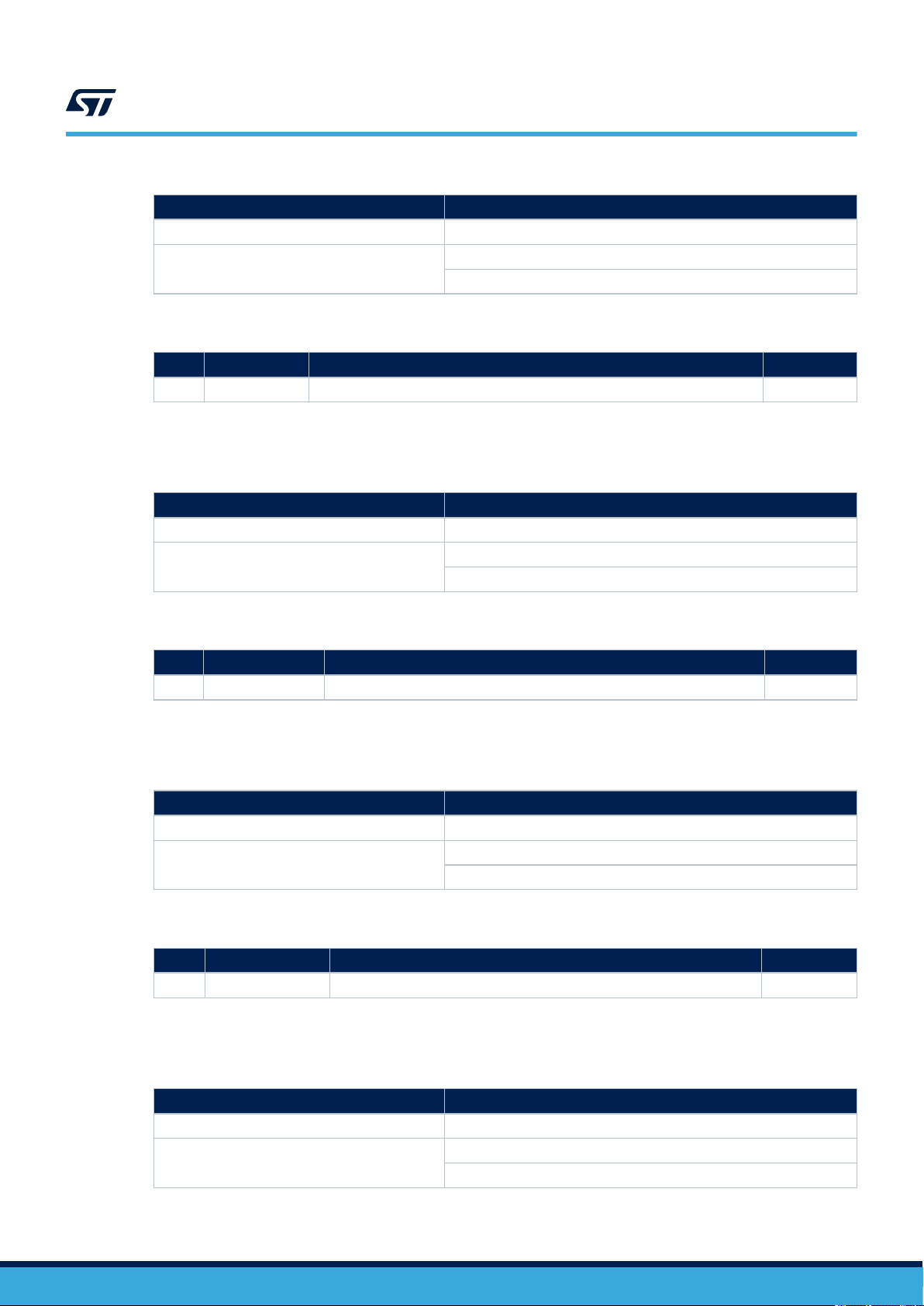
RF command Access type
ReadConfiguration @(FID=03h, PID=01h) R : if the CONFIG security session is open and LCK_TD=0b
WriteConfiguration @(FID=03h, PID=01h)
Table 39. TD_SEAL_MSG content
Bit Name Function Factory value
b15-b0 TD_SEAL_MSG Value of TD_EVENT displayed before first occurence of a TD_UNSEAL event 3030h
Note: Refer to Table 4. List of configuration registers for the TD_SEAL_MSG register.
Table 40. TD_UNSEAL_MSG access
RF command Access type
ReadConfiguration @(FID=03h, PID=02h) R : if the CONFIG security session is open and LCK_TD=0b
WriteConfiguration @(FID=03h, PID=02h)
W : if the CONFIG security session is open and LCK_TD=0b
W effective time : immediate
W : if the CONFIG security session is open and LCK_TD=0b
W effective time : immediate
Table 41. TD_UNSEAL_MSG content
Bit
b15-b0 TD_UNSEAL_MSG Value of TD_EVENT displayed after first occurrence of a TD_UNSEAL event 5555h
Name Function Factory value
Note: Note: Refer to Table 4. List of configuration registers for the TD_UNSEAL_MSG register.
Table 42. TD_RESEAL_MSG access
RF command
ReadConfiguration @(FID=03h, PID=03h) R : if the CONFIG security session is open and LCK_TD=0b
WriteConfiguration @(FID=03h, PID=03h)
W : if the CONFIG security session is open and LCK_TD=0b
W effective time : immediate
Access type
Table 43. TD_RESEAL_MSG content
Bit
b15-b0 TD_RESEAL_MSG Value of TD_EVENT displayed after occurrence of a TD_RESEAL event 5252h
Name Function Factory value
Note: Note: Refer to Table 4. List of configuration registers for the TD_RESEAL_MSG register.
Table 44. TD_SHORT_MSG access
DS13304 - Rev 3
RF command
ReadConfiguration @(FID=03h, PID=04h) R : if the CONFIG security session is open and LCK_TD=0b
WriteConfiguration @(FID=03h, PID=04h)
W : if the CONFIG security session is open and LCK_TD=0b
W effective time : immediate
Access type
page 23/87
ST25TV02KC ST25TV512C
Table 45. TD_SHORT_MSG content
Bit Name Function Factory value
b7- b0 TD_SHORT_MSG
Note: Note: Refer to Table 4. List of configuration registers for the TD_SHORT_MSG register.
RF command Access type
ReadConfiguration @(FID=03h, PID=05h) R : if the CONFIG security session is open and LCK_TD=0b
WriteConfiguration @(FID=03h, PID=05h)
Bit Name Function Factory value
b7- b0 TD_OPEN_MSG
Message displayed when the tamper loop was in closed status during the latest
boot sequence
Table 46. TD_OPEN_MSG access
W : if the CONFIG security session is open and LCK_TD=0b
W effective time : immediate
Table 47. TD_OPEN_MSG content
Message displayed when the tamper loop was in open status during the latest boot
sequence
Tamper detection
63h
6Fh
Note: Refer to Table 4. List of configuration registers for the TD_OPEN_MSG register.
Table 48. TD_STATUS access
RF command
ReadConfiguration @(FID=03h, PID=06h) R : always possible
- W : no write access
Table 49. TD_STATUS content
Bit
b15-b0 TD_EVENT
b23-b16 TD_LOOP
Name Function Factory value
TD_SEAL_MSG, TD_UNSEAL_MSG or TD_RESEAL_MSG
according to result of tamper event detection
TD_SHORT_MSG or TD_OPEN_MSG
according to the status of the tamper loop during the latest boot sequence
Note: Refer to Table 5. List of system registers for the TD_STATUS register.
5.3.2 Tamper detection description
The tamper detection feature allows to check the shortage status between the TD0 and TD1 pins of the
ST25TV02KC-T, and monitor tamper events.
See Section 8.2 RF electrical parameters for recommended impedance values Ropen and Rclosed in cases of
open and closed tamper loop.
The shortage status TD_LOOP and event status TD_EVENT are read in the response to a ReadConfiguration
request with FID=03h and PID=06h.
This is the customer responsibility to check the values of TD_LOOP and TD_EVENT and behave accordingly.
Access type
Not applicable
Not applicable
DS13304 - Rev 3
page 24/87

ST25TV02KC ST25TV512C
Augmented NDEF
TD_LOOP
The shortage status TD_LOOP is captured by ST25TV02KC-T each time that the device is powered- up. Value of
TD_LOOP is equal to value of:
• TD_SHORT_MSG when TD0 and TD1 were connected at capture time
• TD_OPEN_MSG when TD0 and TD1 were not connected at capture time
This information will be lost during power off (no permanent storage of TD_LOOP).
TD_EVENT
The TD_EVENT status is used to monitor the first occurrences of TD_UNSEAL and TD_RESEAL events defined
as follows:
• TD_UNSEAL: TD_EVENT_UPDATE_EN register was set to 1b, and TD0 and TD1 were not connected at
capture time
• TD_RESEAL: TD_EVENT_UPDATE_EN register was set to 1b, TD_UNSEAL already occurred, and TD0
and TD1 were connected at capture time
On factory delivery, TD_EVENT_UPDATE_EN is set to 0b and TD_EVENT is set to the value of TD_SEAL_MSG.
When the first TD_UNSEAL event occurs, TD_EVENT is updated to the value of TD_UNSEAL_MSG.
When the first TD_RESEAL event occurs, TD_EVENT is updated to the value of TD_RESEAL_MSG.
The update of the TD_EVENT register occurs during the RF boot sequence, and its value is stored in the
EEPROM of the ST25TV02KC-T device.
When the LCK_TD register is set to 1b, the TD_EVENT_UPDATE_EN, TD_SEAL_MSG, TD_UNSEAL_MSG,
TD_RESEAL_MSG, TD_SHORT_MSG and TD_OPEN_MSG registers are locked.
Note: When TD_EVENT is updated, the duration of the RF boot sequence t
parameters) is:
• compliant with the 5ms guard-time value defined in the NFC Forum [DIGITAL] specification
• not compliant with the 1ms guard-time value defined in the ISO15693 specification
Note: When TD_EVENT_UPDATE_EN and UTC_EN registers are set to 0b, no programmation of the EEPROM
occurs during the RF boot sequence, and its duration is compliant with the 1ms guard-time value defined in the
ISO15693 specification.
Note: Tamper detection events occurring outside of the capture window (for instance while the IC is in POWER-OFF
state, or during the RF session following the boot sequence) are not detected by the ST25TV02KC-T.
(see Section 8.2 RF electrical
Boot_RF
5.4
Augmented NDEF
5.4.1 Augmented NDEF registers
RF command Access type
ReadConfiguration @(FID=04h, PID=00h) R : always possible
WriteConfiguration @(FID=04h, PID=00h)
DS13304 - Rev 3
Table 50. ANDEF_EN access
W : if the CONFIG security session is open and LCK_ANDEF=0b
W effective time : on next RF boot sequence
page 25/87
Table 51. ANDEF_EN content
Bit Name Function Factory value
b0 ANDEF_EN
0: ANDEF feature is disabled,
1: ANDEF feature is enabled
b7- b1 RFU - 0000000b
Note: Refer to Table 4. List of configuration registers for the ANDEF_EN register.
Table 52. ANDEF_CFG access
RF command Access type
ReadConfiguration @(FID=04h, PID=01h) R : always possible
WriteConfiguration @(FID=04h, PID=01h)
W : if the CONFIG security session is open and LCK_ANDEF=0b
W effective time : on next RF boot sequence
Table 53. ANDEF_CFG content
ST25TV02KC ST25TV512C
Augmented NDEF
0b
Bit Name Function Factory value
b0 ANDEF_UID_EN
b1 ANDEF_CUS_EN
b2 ANDEF_UTC_EN
0: UID field disabled in ANDEF feature
1: UID field enabled in ANDEF feature
0: Custom field disabled in ANDEF feature
1: Custom field enabled in ANDEF feature
0: Unique tap code field disabled in ANDEF feature
1: Unique tap code field enabled in ANDEF feature
b3 RFU - 0b
0: Tamper detection field disabled in ANDEF feature
b4
ANDEF_TD_EN
b5 ANDEF_SEP_EN
(1)
1: Tamper detection field enabled in ANDEF feature
0: ANDEF field separator disabled
1: ANDEF field separator enabled
b7- b6 ANDEF_BYTE Byte offset in block ANDEF_BLOCK where the ANDEF feature starts operating 00b
b15-b8 ANDEF_BLOCK Block address where the ANDEF feature starts operating 00h
1. relevant on ST25TV02KC-T devices only, forced to 0b on ST25TVxxxC-A devices
Note: Refer to Table 4. List of configuration registers for the ANDEF_CFG register.
Table 54. ANDEF_SEP access
0b
0b
0b
0b
1b
DS13304 - Rev 3
RF command
Access type
ReadConfiguration @(FID=04h, PID=02h) R : if the CONFIG security session is open and LCK_ANDEF=0b
WriteConfiguration @(FID=04h, PID=02h)
W : if the CONFIG security session is open and LCK_ANDEF=0b
W effective time : immediate
Table 55. ANDEF_SEP content
Bit
b7- b0 ANDEF_SEP Character used as ANDEF field separator when ANDEF_SEP_EN=1b 78h
Name Function Factory value
page 26/87
ST25TV02KC ST25TV512C
Note: Refer to Table 4. List of configuration registers for the ANDEF_SEP register.
Table 56. ANDEF_CUSTOM_LSB access
RF command Access type
ReadConfiguration @(FID=04h, PID=03h) R : if the CONFIG security session is open and LCK_ANDEF=0b
WriteConfiguration @(FID=04h, PID=03h)
Table 57. ANDEF_CUSTOM_LSB content
Bit Name Function Factory value
b31-b0 ANDEF_CUSTOM_LSB First 4 characters of the ANDEF custom field 2E2E2E2Eh
Note: Refer to Table 4. List of configuration registers for the ANDEF_CUSTOM_LSB register.
Table 58. ANDEF_CUSTOM_MSB access
W : if the CONFIG security session is open and LCK_ANDEF=0b
W effective time : immediate
Augmented NDEF
RF command Access type
ReadConfiguration @(FID=04h, PID=04h) R : if the CONFIG security session is open and LCK_ANDEF=0b
WriteConfiguration @(FID=04h, PID=04h)
W : if the CONFIG security session is open and LCK_ANDEF=0b
W effective time : immediate
Table 59. ANDEF_CUSTOM_MSB content
Bit
b31-b0 ANDEF_CUSTOM_MSB Last 4 characters of the ANDEF custom field 2E2E2E2Eh
Name Function Factory value
Note: Refer to Table 4. List of configuration registers for the ANDEF_CUSTOM_MSB register.
Table 60. ANDEF_UID access
RF command
ReadSingleBlock
ReadMultipleBlocks
- W : no write access
R : if ANDEF_EN=1b and ANDEF_UID_EN=1b
Access type
Table 61. ANDEF_UID content
Bit
b127-b0 ANDEF_UID Value displayed in the UID field of the ANDEF feature UID in ASCII format starting with "E0"
Name Function Factory value
Note: Refer to Table 5. List of system registers for the ANDEF_UID register.
DS13304 - Rev 3
page 27/87
 Loading...