

ST25TV02K ST25TV512
Datasheet
NFC Type 5 / RFID tag IC with up to 2-Kbit EEPROM, product identification and
protection
Features
Contactless interface
• Based on ISO/IEC 15693
• NFC Forum Type 5 tag certified by the NFC Forum
• Supports all ISO/IEC 15693 modulations, coding, subcarrier modes and data
rates
• Custom Fast read access up to 53 Kbit/s
• Single and multiple block reads
Wafer
• Single block writes
• Internal tuning capacitance: 23 pF, 99.7 pF
• Proprietary Inventory commands for speeding up the inventory process
Product status link
ST25TV02K
ST25TV512
Memory
• Up to 2 Kbits of EEPROM
• RF interface accesses blocks of four bytes
• Write time from RF: typical 5 ms for one block
• Data retention: 60 years
• Minimum endurance: 100 k write cycles
• 16-bit event counter with anti-tearing
Data protection
• User memory: two or three areas, read and/or write protected by two 32-bit
encrypted passwords for three areas or one 64-bit encrypted password for two
areas
• System configuration: write protected by a 32-bit encrypted password
• Permanent write locks at a block level
Product identification and protection
• Kill mode and untraceable mode
• Tamper detect capability (patent pending)
• TruST25 digital signature
• EAS (electronic article surveillance) capability
Privacy protection
• Consumer privacy can be protected through the following features:
– Kill mode
– Untraceable mode
• In association with:
– Passwords with cover coding
– Data and configuration locks (permanent or temporary)
Temperature range
• From - 40 to 85 °C
DS12074 - Rev 11 - February 2021
For further information contact your local STMicroelectronics sales office.
www.st.com

ST25TV02K ST25TV512
Package
• Sawn and bumped wafer, ECOPACK2 (RoHS compliant)
• 5-pin package, ECOPACK2 (RoHS compliant)
Compatibility ST25TV02K / LRI2K
• Full compatibility in terms of functionality and capacitances with two exceptions:
– Kill command requires option_flag to be set to 0
– Error codes and error generation can be different on a per command basis
DS12074 - Rev 11
page 2/90
1 Description
ST25TV02K and ST25TV512 are NFC/RFID tag ICs with a tamper-proof feature, and specific modes to protect
tag access, such as Untraceable mode.
These devices feature a digital signature used to prove the origin of the chip in cloning detection, embed a
configurable EEPROM with 60-year data retention, and can be operated from a 13.56 MHz long-range RFID
reader or an NFC phone.
The contactless interface is compatible with the ISO/IEC 15693 standard and NFC Forum Type 5 tag.
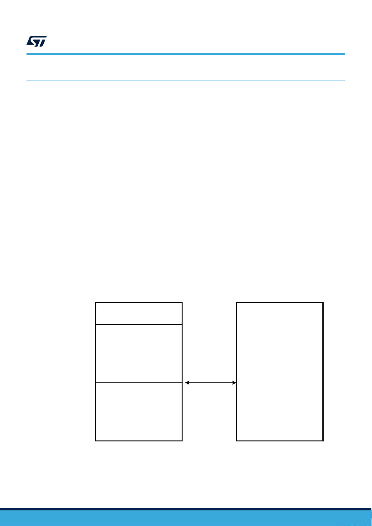
1.1 ST25TV02K/512 block diagram (with tamper detect)
Figure 1. ST25TV02K/512 (with tamper detect) block diagram
ISO 15693
ST25TV02K ST25TV512
Description
EEPROM
xxx-bit
256 bits
(EAS)
RF Tag
Long Range
256 bits
signature
2x32-bit password
(1)
TD
(tamper detect)
1. tamper detect is optional.
Table 1. Signal names
Signal name
AC0 Antenna coil I/O
AC1 Antenna coil I/O
TD0 Tamper detect loop I/O
TD1 Tamper detect loop I/O
Function Direction
DS12074 - Rev 11
page 3/90
ST25TV02K ST25TV512
ST25TV02K/512 block diagram (with tamper detect)
Figure 2. DFN5 package connections diagram (with tamper detect)
TD0
NC
AC0
1: Not Connected
Figure 3. Die connections for sawn and bumped wafer (bottom view)
1
2
ABCD
XYZW
3 4
Top view
(marking side)
AC0 TD0
AC1 TD1
TD11
5
1
NC
2
AC1
5
2
Bottom view
(pads side)
AC0 NC
AC1 NC
With tamper detect Without tamper detect
1
2
34
DS12074 - Rev 11
page 4/90

2 Description of signals
2.1 Antenna coil (AC0, AC1)
These inputs are used exclusively to connect the ST25TV02K/512 devices to an external coil. It is advised not to
connect any other DC or AC path to AC0 or AC1.
When correctly tuned, the coil is used to power and access the device using the ISO/IEC 15693 and ISO 18000-3
mode 1 protocols.
2.2 Tamper detect (TD0, TD1)
These inputs are used to connect a wire loop to the ST25TV02K/512 devices to detect an open or a short
between the two pins TD0, TD1.
ST25TV02K ST25TV512
Description of signals
DS12074 - Rev 11
page 5/90
3 Power management
3.1 Device set
To ensure a proper boot of the RF circuitry, the RF field must be turned ON without any modulation for a minimum
period of time t
power-up sequence).
. Before this time, ST25TV02K/512 ignores all received RF commands. (See Figure 4. RF
boot_RF
ST25TV02K ST25TV512
Power management
Figure 4. RF power-up sequence
RF interface ready
Power-up
by RF
3.2 Device reset
To ensure a proper reset of the RF circuitry, the RF field must be turned off (100% modulation) for a minimum
t
RF_OFF
period of time.
RFfield
Vint_supply
None Access
Allowed RF
t
boot_RF
RF REQUEST
RF ANSWER
DS12074 - Rev 11
page 6/90
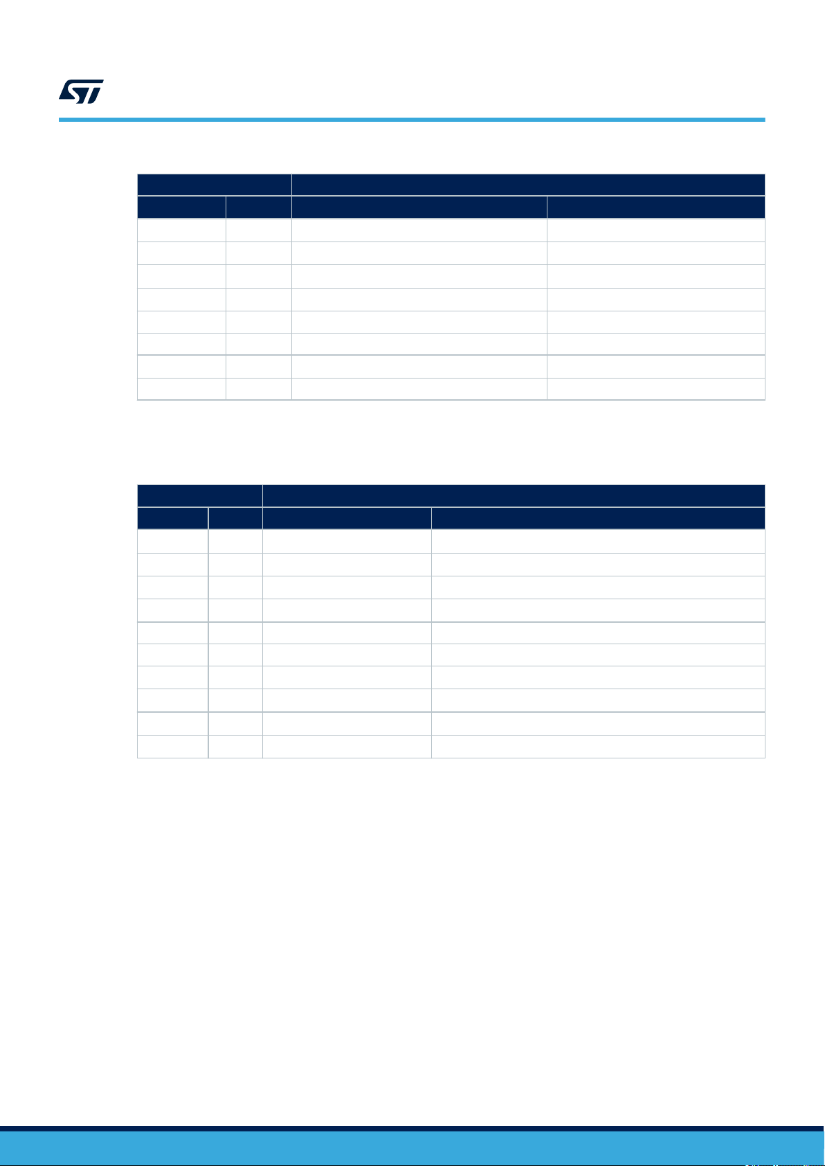
4 Memory management
4.1 Memory organization overview
The ST25TV02K/512 memory is divided in two main memory areas:
• User memory
• System configuration area
The ST25TV02K/512 user memory can be divided into two or three user areas. Area 0 starts at address 0, it has
1 block size, it is always readable, and it can be locked.
The rest of the user memory can be either configured as one single area (Area 1) and can be read - and/or
- write-protected with one 64-bit password, or configured as two areas (Area 1 and Area 2), which can be
individually read - and/or - write-protected with a 32-bit password each. When Area 2 exists, Area 2 starts at the
block number corresponding to half the user memory.
Furthermore, each block can be locked permanently and individually for larger flexibility in number of areas
The ST25TV02K/512 system configuration area contains registers to configure all ST25TV02K/512 features,
which can be tuned by user. Its access is protected by a 32 bit configuration password.
This system configuration area also includes read only device information such as IC reference, memory size,
as well as a 64-bit block that is used to store the 64-bit unique identifier (UID), the AFI (default 00h) and DSFID
(default 00h) registers, the TruST25™ digital signature. The UID is compliant with the ISO 15693 description, and
its value is used during the anticollision sequence (Inventory). The UID value is written by ST on the production
line. The AFI register stores the application family identifier. The DSFID register stores the data storage family
identifier used in the anticollision algorithm.
The system configuration area includes blocks that store up to two RF user area access passwords and a RF
configuration password.
ST25TV02K ST25TV512
Memory management
Area 0:
1 block (always readable)
Area 1
User memory
(EEPROM up
to 2-Kbits)
Password
protected
Area 2
Note: Each block can be individually locked
Figure 5. Memory organization
Half user
memory
Area 0:
1 block (always readable)
Area 1
DS12074 - Rev 11
page 7/90
4.2 User memory
User memory is addressed as blocks of 4 bytes, starting at address 0. Table 2. 2Kb user memory as seen by RF
shows how memory is seen from RF interface.
ST25TV02K ST25TV512
User memory
Table 2. 2Kb user memory as seen by RF
RF command
(block addressing)
Read Single Block
Read Multiple Blocks
Fast Read Single Block
Fast Read Multiple Blocks
Write Single Block
Inventory Read
Fast Inventory Read
4.2.1 User memory areas
The user memory can be split into two or three different areas as showed in Table 3. Memory Organization
RF block 00h
Byte
0003h
RF block 01h
Byte
0007h
RF block 02h
Byte
0011h
....
RF block 3Fh
Byte
03FFh
Byte
0002h
Byte
0006h
Byte
0010h
Byte
03FEh
User memory
Byte
0001h
Byte
0005h
Byte
0009h
Byte
03FDh
Byte
0000h
Byte
0004h
Byte
0008h
Byte
03FCh
Part Number
ST25TV512
ST25TV02K Block 0 Block 1 to 31 Block 32 to 63 Block 0 Block 1 to 63
Area 0 Area 1 Area 2 Area 0 Area 1
Block 0 Block 1 to 7 Block 8 to 15 Block 0 Block 1 to 15
Each area has a distinct access privilege as explained below:
• Area 0 is always readable. It can be locked.
• Areas 1 and 2 can be protected in read and/or write access by password.
Each block of Areas 1 and 2 can be individually locked (see Section 5.2 Data protection).
4.3 System configuration area
In addition to the user memory, the ST25TV02K/512 include a set of registers located in the system configuration
area memory (EEPROM nonvolatile registers). These registers are set during device configuration (i.e.: area
extension), or by the application (i.e.: area protection)., their content is read during the boot sequence and defines
basic ST25TV02K/512 behaviour.
The registers located in the system configuration area can be accessed via dedicated Read Configuration and
Write Configuration commands, with a pointer acting as the register address.
The configuration security session must first be open, by presenting a valid configuration password, to grant write
access to system configuration registers.
Table 4 shows the complete map of the system configuration area.
Table 3. Memory Organization
Three areas configuration Two areas configuration
DS12074 - Rev 11
page 8/90
ST25TV02K ST25TV512
System configuration area
Table 4. System configuration memory map accessible through write_cfg and read_cfg commands
RF access Static Register
Address Type Name Function
00h
01h
02h
03h
04h RO Table 23. CNT_VAL Counter Value
05h RO Table 24. TAMPER_DETECT Tamper Detect
06h
07h RO Table 21. KID Key identifier
1. Write access is granted if RF configuration security session is open and configuration is not locked (LOCK_CFG register
equals to 0).
Table 5. System configuration memory map for registers accessed through dedicated commands
RW
RW
RW
RW
RW
(1)
(1)
(1)
(1)
(1)
Table 8. A1SS Area 1 access protection
Table 9. A2SS Area 2 access protection
Table 17. EAS_SEC EAS Security
Table 22. CNT_CFG Counter Configuration
Table 10. LOCK_CFG Configuration locked
RF access Static Register
Address Type Name Function
N/A
N/A
N/A
N/A
WO
WO
WO
WO
(1)
Table 25. LOCK_DSFID DSFID lock status
(2)
Table 26. LOCK_AFI AFI lock status
(1)
Table 27. DSFID DSFID value
(2)
Table 28. AFI AFI value
N/A RO Table 29. IC_REF IC reference value
N/A RO Table 30. UID Unique identifier, 8 bytes
WO
WO
WO
WO
(3)
Table 7. PWD_KILL Kill or untraceable password, 4 bytes
(4)
Table 12. PWD_A1 User Area 1 security session password, 4 bytes
(3)
Table 13. PWD_A2 User Area 2 security session password, 4 bytes
(3)
Table 11. PWD_CFG Configuration security session password, 4 bytes
N/A
N/A
N/A
N/A
1. Write access if DSFID is not locked
2. Write access if AFI is not locked.
3. Write access only if not locked.
4. Write access only if corresponding security session is open.
DS12074 - Rev 11
page 9/90

5 ST25TV02K/512 specific features
ST25TV02K/512 offer the data protection feature, both user memory and system configuration, a kill mode, and a
untraceable mode.
Those features can be programmed by setting registers of the ST25TV02K/512. ST25TV02K/512 can be partially
customized using configuration registers located in the EEPROM system area.
These registers are dedicated to:
• Data Memory organization and protection AiSS, LOCK_BLOCK.
• Kill mode, KILL
• The device’s structure LOCK_CFG
• Electronic Article Surveillance (EAS)
• TruST25™ digital signature
• Counter
• Tamper Detect
• Random Number generation
• Untraceable mode
A set of additional registers allows to identify and customize the product (DSFID, AFI, IC_REF, etc.).
Dedicated commands Read Configuration and Write Configuration must be used to access the configuration
registers. Update is only possible when the access right has been granted by presenting the configuration
password (PWD_CFG), and if the system configuration was not previously locked (LOCK_CFG=1).
After any valid write access to the configuration registers, the new configuration is immediately applied.
ST25TV02K ST25TV512
ST25TV02K/512 specific features
5.1
Kill mode
5.1.1 Kill registers
Table 6. KILL
RF
Bit Name Function Factory value
N/A KILL_MUTE Status of the KILL feature Inactive
RF
Bit Name Function Factory value
b31-b0 KILL_PSWD Password value for kill feature or untraceable mode 00000000h
Note: Refer to Table 5. System configuration memory map for registers accessed through dedicated commands .
Command Kill (cmd code A6h) UID @00h
Type WO if PWD_KILL is correctly presented in the Kill command.
Table 7. PWD_KILL
Command Write pswd (cmd code B1h) with pswd_id = 0h
Type WO: only possible if PWD_KILL is not locked.
DS12074 - Rev 11
page 10/90

5.1.2 Kill mode description
KILL register allows the user to permanently kill the ST25TV02K/512 tag.
Two working modes are offered by ST25TV02K/512:
• Kill mute mode:
– When KILL_MUTE is set with the Kill command code, the ST25TV02K/512 are killed. They can not be
read or written and stays mute to any request. Kill mute mode is definitive.
• Normal mode:
– In normal usage, KILL_MUTE is set to 0, ST25TV02K/512 will process the request and respond
accordingly.
The Kill Password PWD_KILL must be presented in the Kill command for setting the Kill Mute mode.
Kill Password lock
By default, the Kill password is not write protected. The kill password can be locked with Lock kill (cmd code B2h).
For safe operation, it is recommended to change the default value of the Kill Password and lock it even if not used
in the final product
When not used in an end application, a random value should be written into the KILL_PWD and the KILL_PWD
should be locked with Lock kill.
5.2 Data protection
ST25TV02K/512 provide a special data protection mechanism based on encrypted passwords that unlock
security sessions.
User memory can be protected for read and/or write access and system configuration can be protected from write
access. User memory can also be permanently locked. Each block can be independently locked from each other
with the Lock block command (refer to Section 6.4.8 Lock block).
ST25TV02K ST25TV512
Data protection
5.2.1 Data protection registers
Table 8. A1SS
RF
Bit Name Function Factory value
b1-b0 RW_PROTECTION_A1
b2 MEM_ORG
b7-b3 RFU - 00000b
Command
Type R always, W if configuration security session is open and configuration not locked
Read Configuration (cmd code A0h) @00h
Write Configuration (cmd code A1h) @00h
Area 1 access rights:
00: Area 1 access: Read is always allowed / Write always allowed
01: Area 1 access: Read is always allowed and if user security
session is open (i.e. the proper area 1 password has been presented),
write is allowed.
10: Area 1 access: Read and Write are allowed only if user security
session is open (the proper area 1 password has been presented).
11: Area 1 access: Read is allowed only if user security session is
open (the proper area 1 password has been presented). Write is
always forbidden.
0: memory is split in three areas (Areas 0, 1 and 2)
1: memory is composed of two areas (Areas 0 and 1)
00b
1b
Note: Refer to Table 4. System configuration memory map accessible through write_cfg and read_cfg commands
DS12074 - Rev 11
page 11/90

Table 9. A2SS
ST25TV02K ST25TV512
Data protection
RF
Bit Name Function Factory value
b1-b0 RW_PROTECTION_A2
b7-b2 RFU - 000000b
Command
Type R always, W if configuration security session is open and configuration not locked
Read Configuration (cmd code A0h) @01h
Write Configuration (cmd code A1h) @01h
Area 2 access rights:
00: Area 2 access: Read and write are always allowed
01: Area 2 access: Read is always allowed, and if the user
security session is open (i.e. the proper Area 2 password has been
presented), then write is allowed.
10: Area 2 access: Read and Write are allowed only if the user
security session is open (the proper Area 2 password has been
presented)
11: Area 2 access: Read is allowed only if user security session is
open (the proper Area 2 password has been presented). Write is
always forbidden.
00b
Note: Refer to Table 4. System configuration memory map accessible through write_cfg and read_cfg commands
Table 10. LOCK_CFG
Command
RF
Type
Bit Name Function Factory value
b0 LCK_CFG
b7-b1 RFU - 0000000b
Read Configuration (cmd code A0h) @06h
Write Configuration (cmd code A1h) @06h
R: always possible
W: if RF configuration security session is open (configuration password has been presented
before) and configuration not locked
0: Configuration is unlocked (configuration registers can be written)
1: Configuration is locked (configuration registers are definitively
locked)
0b
Note: Refer to Table 4. System configuration memory map accessible through write_cfg and read_cfg commands
Table 11. PWD_CFG
Command Write pswd (cmd code B1h) with pswd_id = 3h
RF
Bit Name Function Factory value
b31-b0 CFG_PSWD Password value for configuration area 00000000h
Type
WO: if RF configuration security session is open (configuration password has been presented
before). If the configuration is locked, and the EAS configuration is protected by password, the
new PWD_CFG value is only applicable to the EAS configuration.
Note: Refer to Table 5. System configuration memory map for registers accessed through dedicated commands
DS12074 - Rev 11
page 12/90
Table 12. PWD_A1
ST25TV02K ST25TV512
Data protection
RF
Bit Name Function Factory value
b31-b0 A1_PSWD
Command Write pswd (cmd code B1h) with pswd_id = 1h
Type WO: if RF area 1 security session is open (area 1 password has been presented before).
When MEM_ORG=0: Password value for user area 1
When MEM_ORG=1: 32 least significant bits of the 64-bit Password
value for user area 1
00000000h
Note: Refer to Table 5. System configuration memory map for registers accessed through dedicated commands
Table 13. PWD_A2
Command Write pswd (cmd code B1h) with pswd_id = 2h
RF
Bit Name Function Factory value
b31-b0 A2_PSWD
Type
WO: if RF area 2 security session is open (area 2 password has been presented before). Only
applicable to the case of MEMORG=0
When MEM_ORG=0: Password value for user area 2 in case of three
area memory setup
When MEM_ORG=1: 32 most significant bits of area 1 password in
case of two area memory setup
(in this last case area 1 password is 64-bit long)
00000000h
Note: Refer to Table 5. System configuration memory map for registers accessed through dedicated commands .
5.2.2 Passwords and security sessions
ST25TV02K/512 provide protection of user memory and system configuration registers. The users can access
those protected data by opening security sessions with the help of passwords. Access rights are more restricted
when security sessions are closed, and less restricted when security sessions are open.
There are two types of security sessions, as shown in Table 14:
Table 14. Security session type
Security session Open by presenting
user
configuration
1. Write access to the password number corresponding to the password number presented.
password Area 1, Area 2
(PWD_A1, PWD_A2)
Configuration password
(PWD_CFG)
In a three areas set up (MEM_ORG set at 0), each of the User Area 1 and 2 passwords is 32-bits long, and
default factory passwords value is 00000000h.
In a two areas setup (MEM_ORG set at 1), User Area 1 password is 64-bits long, and default factory password
value is 0000000000000000h.
The ST25TV02K/512 passwords management is organized around dedicated set of commands to access the
dedicated registers in system configuration area.
The dedicated password commands are:
• Write Password command (code B1h): See Section 6.4.20 Write Password.
• Present Password command (code B3h): See Section 6.4.21 Present Password
User possible actions for security sessions are:
Right granted when security session is open, and until it is
user access to protect user memory as defined in AiSS registers
user write access to password A1 or A2
user write access to configuration registers
closed
(1)
DS12074 - Rev 11
page 13/90
ST25TV02K ST25TV512
Data protection
• Open user security session: Present Password command, with password identifier 1 for PWD_A1 and 2
for PWD_A2 for three areas configuration or identifier 1 for PWD_A1 for two areas configuration, and the
valid corresponding password
• Write password:
– When MEMORG=0:
Present Password command, with password identifier 1 for PWD_A1 and 2 for PWD_A2 and the
current valid corresponding password. Then Write Password command, with same password number
(1 or 2) and the new corresponding password.
– When MEMORG=1:
present PWD_A1 (64 bits), then Write Password command with PWD_A1 and then PWD_A2
• Close user security session: Present Password command, with a different password number than the one
used to open session or any wrong password. Or remove tag from RF field (POR).
• Open configuration security session: Present Password command, with password number 3 and the valid
password PWD_CFG.
• Close configuration security session: Present Password command, with a password number different
than 3, or password number 3 and wrong password PWD_CFG. Or remove tag from field (POR).
Opening any new security session (user or configuration) automatically close the previously open one (even if it
fails).
Figure 6. Security sessions management
Present any
password not OK
Any other
command
Any other
command
PWD_x OK
Any other
command
Present
ST25TVxxx
out of RF field
Field ON
All security
sessions
closed
PWD_x OK
Security
session x
opened
(y closed)
Security
session y
opened
(x closed)
Field OFF
Present
Present
PWD_y OK
DS12074 - Rev 11
page 14/90

5.2.3 User memory protection
On factory delivery, areas are not protected.
Each area can be individually protected in read and/or write access.
Area 0 is always readable.
Furthermore, Area 0 can be independently write locked.
Each memory area can also have individual Read/Write access conditions.
For each area 1 and 2, an AiSS register is used to:
• Select the protection against read and write operations for this area
(See Table 8. A1SS, and Table 9. A2SS for details about available read and write protections).
When updating AiSS registers, the new protection value is effective immediately after the register write
completion.
• Block 0 is an exception to this protection mechanism:
– Block 0 can be individually write locked by issuing a Lock Single Block command. Once locked, it
cannot be unlock.
– User needs no password to lock block 0.
– Locking block 0 is possible even if the configuration is locked (LOCK_CFG=1).
– Unlocking Area 1 (through A1SS register) does not unlock block 0 if it has been locked though Lock
Block command.
– Once locked, the user cannot unlock block 0.
• Other blocks can be individually locked.
ST25TV02K ST25TV512
Data protection
Retrieve the security status of a user memory block or byte
User can read a block security status by issuing following commands:
• Get Multiple Blocks Security Status command
• (Fast) Read Single Block with option flag set to 1
• (Fast) Read Multiple Blocks with option flag set to 1
• (Fast) Inventory Read
ST25TV02K/512 responds with a Block security status containing a Lock_bit flag as specified in ISO 15693
standard. This lock_bit flag is set to 1 if block is locked against write.
Lock_bit flag value may vary if corresponding user security session is open or closed.
5.2.4 System memory protection
By default, the system memory is write protected, except the kill password and the EAS settings.
Th system memory consists of all the registers defined in Table 4. System configuration memory map accessible
through write_cfg and read_cfg commands. Some registers are read-only and can never be written.
To enable write access to system configuration registers, which have write capability, user must open the
configuration security session (by presenting a valid password 3) and system configuration must not be locked
(LOCK_CFG=00h).
By default, user can read all system configuration registers, except all passwords, LOCK_DSFID and LOCK_AFI.
Configuration lock:
• Write access to system configuration registers can be locked by writing 01h in the LOCK_CFG register.
• User cannot unlock system configuration if LOCK_CFG=01h, even after opening configuration security
session (Lock is definitive).
• When system configuration is locked (LOCK_CFG=01h), it is still possible to change passwords (0 to 3).
Device identification registers:
• AFI and DFSID registers can be independently locked by user, issuing respectively a Lock AFI and a Lock
DSFID command. Lock is definitive: once locked, AFI and DSFID registers cannot be unlocked.
• Other device identification registers (MEM_SIZE, BLK_SIZE, IC_REF, UID) are read only registers.
DS12074 - Rev 11
page 15/90
ST25TV02K ST25TV512
Untraceable mode
5.3 Untraceable mode
5.3.1 Untraceable mode register
Table 15. Untraceable mode register
Command Enable untraceable mode (cmd code BAh) with pswd_id = 0h
RF
Bit Name Function Factory value
b31-b0
Type
UNTRACEABLE
_MODE_PSWD
Note: Refer to Table 5. System configuration memory map for registers accessed through dedicated commands for the
untraceable mode register.
5.3.2 Untraceable mode description
With the EnableUntraceableMode command, the ST25TV02K/512 do not respond to any command except
Present Password and Get Random Number, guaranteeing the untraceability to customer requests.
The EnableUntraceableMode command requires the untraceable access code (fixed value) and the crypted
untraceable mode password to be presented for ST25TV02K/512 to enter into this mode.
To get out of the mode, the valid crypted untraceable mode password has to be transmitted to ST25TV02K/512
with the Present password command. The crypted untraceable mode password is obtained from the random
number and the untraceable mode password as explained in AN5103 "Password encryption for ST25TV512 and
ST25TV02K devices", available on www.st.com. When not used in an end application, a random value must be
written into the KILL_PWD password, and the KILL_PWD must be locked with Lock kill.
WO : only possible if untraceable mode password has been written before, always
writable otherwise
Password value for feature untraceable mode 00000000h
5.4 Random number
5.4.1 Random number register
Table 16. Random number register
RF
Bit Name Function Factory value
b15-b0 RANDOM_NUMBER 16-bit random number generated by ST25TV02K/512 N/A
Note: Refer to Table 5. System configuration memory map for registers accessed through dedicated commands for the
random number register.
5.4.2 Random number description
The GET_RANDOM_NUMBER returns a 16-bit random number.
Command Get random number (cmd code B4h)
Type RO: is only possible with Get random number command.
DS12074 - Rev 11
page 16/90

5.5 Electronic article surveillance (EAS)
5.5.1 EAS registers
Table 17. EAS_SEC
ST25TV02K ST25TV512
Electronic article surveillance (EAS)
Command
Type
Bit Name Function Factory value
b0 W_PROTECTION_EAS
b7-b1 RFU - 0000000b
Read Configuration (cmd code A0h) @02h
Write Configuration (cmd code A1h) @02h
R: always possible
W: if RF configuration security session is open (the proper configuration password has been
presented before) and configuration not locked
EAS security write protection:
0: EAS parameters are always writable
1: EAS parameters are write protected by configuration password.
In case of lock_EAS command has been previously used, this bit is
don’t care and EAS parameters are non-writable.
0b
Note: Refer to Table 4. System configuration memory map accessible through write_cfg and read_cfg commands for
the AES security activation register.
Table 18. EAS_TELEGRAM register
Enable EAS (cmd code A5h) with option flag set to 0
Command
RF
Type
Bit Name Function Factory value
b255-b0 EAS_TELEGRAM Electronic article surveillance telegram. All bits = 0b
Enable EAS (cmd code A5h) with option flag set to 1 and mask length ≠ 00h and EAS_ID
Write Single (cmd code 21h) to Blocks [248 to 255]
Read Single blocks at @248 to 255 returns an error.
R: possible with enable EAS command only if set EAS command has been presented before
W: possible under conditions set in the EAS_SEC configuration register and EAS
configuration not locked
(1)
1. Write Single Block at addresses 248 to 255 correspond to EAS blocks 1 to 8 respectively.
5.5.2 EAS ID
Table 19. EAS_ID
Command
RF
Type
Bit Name Function Factory value
b15-b0 EAS_ID Electronic article surveillance identifier value. 0000h
DS12074 - Rev 11
Enable EAS (cmd code A5h) with option flag set to 1 and mask length set to 0h
Write EAS ID (cmd code A7h)
R: possible with enable EAS command only if set EAS command has been presented before
W: possible under conditions set in the EAS_SEC configuration register and EAS
configuration not locked
page 17/90

ST25TV02K ST25TV512
Electronic article surveillance (EAS)
5.5.3 EAS configuration
Table 20. EAS_CFG
Enable EAS (cmd code A5h) with option flag set to 1 and mask length ≠ 00h and EAS_ID, or
Command
RF
Type
Bit Name Function Factory value
b1-b0 EAS_CFG
b15-b2 RFU - 000000b
The EAS parameters (ID, Telegram, mode (set/reset) can be definitely locked with the Lock EAS command (refer
to Section 6.4.27 Lock EAS).
with option flag set to 0
Write EAS config (cmd code A8h)
WO: possible under conditions set in the EAS_SEC configuration register and configuration
not locked
Electronic article surveillance identifier configuration:
00: 256 bit payload (EAS block 1 to 8)
01: 128 bit payload (EAS block 1 to 4)
10: 64 bit payload (EAS block 1 to 2)
11: 32 bit payload (EAS block 1)
00h
5.5.4 EAS description
The EAS (electronic article surveillance) feature is mainly used for library management, applications, requiring an
anti-theft protection.
This is programmable and configured by custom commands and optionally protected by the configuration
password (when programming EAS_SEC to 1) and can be locked.
A telegram can be stored using standard write command depending of its configured length (EAS block 1 – EAS
Block 8).
The EAS feature can be activated, reset, locked using a set of custom commands (see Section 6.4.24 Set EAS,
Section 6.4.25 Reset EAS, Section 6.4.26 Enable EAS, Section 6.4.27 Lock EAS, Section 6.4.28 Write EAS
ID and Section 6.4.29 Write EAS CONFIG).
The EAS feature is reset (deactivated) by default.
DS12074 - Rev 11
page 18/90
EAS – Normal
operation
ST25TV02K ST25TV512
Electronic article surveillance (EAS)
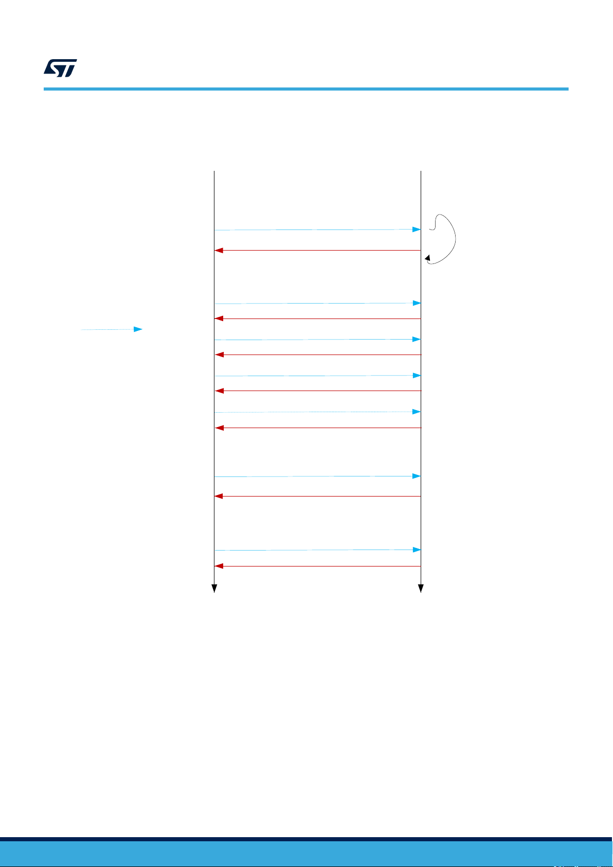
Figure 7. Nominal EAS operation
RF Reader ST25TV
EAS deactivated
(reset)
Optional
step
Write Single (EAS, EAS block x)
Write EAS config
Write EAS ID
Set EAS
Lock EAS
Enable EAS (selective ID or none)
If selected: EAS ID or telegram
Repeated
based on EAS
telegram size
EAS ready
DS12074 - Rev 11
Reset EAS (if not locked)
EAS deactivated
(reset)
By default, the EAS configuration (EAS telegram, EAS ID, EAS configuration, lock EAS, EAS mode) is not write
protected.
The EAS configuration can be write protected by the configuration password (PWD_CFG) by writing 1b1 into the
W_PROTECTION_EAS (EAS_SEC register). If W_PROTECTION_EAS bit is set, the EAS configuration can be
changed only if the configuration password has been presented just before in the same RF session.
Write access to the EAS configuration can be locked by executing the lock_EAS command. User cannot unlock
system configuration if the EAS configuration has already been locked earlier with the Lock_EAS command, even
after opening configuration security session (Lock is definitive).
page 19/90

ST25TV02K ST25TV512
TruST25 digital signature
5.6 TruST25 digital signature
ST25TV02K/512 support TruST25 digital signature, a feature that allows to verify the authenticity of the device,
based on a unique digital signature.
TruST25 solution encompasses secure industrialization processes and tools deployed by STMicroelectronics to
generate, store and check the signature in the device.
Table 21. KID
Command Read Cfg (cmd code A0h) @7h
Bit
b7-b0 KID
Type RO
Name Function Factory value
Contains a key identifier used for TruST25 digital signature
identification and possible revocation.
ST key number
Note: Refer to Table 4. System configuration memory map accessible through write_cfg and read_cfg commands for
the KID register.
5.7 Counter
5.7.1 Counter registers
Counter configuration
Table 22. CNT_CFG
Command
Bit
b0 CNT_EN
b1 CNT_CLR
b7-b2 RFU - 000000b
Type
Name Function Factory value
Read Cfg (cmd code A0h) @3h
Write Cfg (cmd code A1h) @3h
R: always possible
W: if RF configuration security session is open (the proper configuration password has been
presented before) and configuration not locked.
Counter enable
0: counter is disabled
1: counter is enabled on successful write operation (one increment
per RF session)
Counter clear:
0: don’t care
1: counter is cleared and automatically disabled (CNT_EN is put to 0)
This bit is self-cleared
0b
0b
Note: Refer to Table 4. System configuration memory map accessible through write_cfg and read_cfg commands for
the CNT_CFG register.
Counter value
Table 23. CNT_VAL
Bit
DS12074 - Rev 11
Command Read Cfg (cmd code A0h) @4h
page 20/90

ST25TV02K ST25TV512
Inventory Read
Bit
b15-b0 CNT_VAL Counter value 0h
Note: Refer to Table 4. System configuration memory map accessible through write_cfg and read_cfg commands for
the CNT_VAL register.
Type RO
Name Function Factory value
5.7.2 Counter description
A 16 bits counter can track the write events on the NDEF file.
It benefits from an anti-tearing mechanism that ensures the consistency of the counter, even if there is an
electrical problem during its increment.
The value of the counter (CNT_VAL) can be checked by any application, by reading the Counter register.
If enabled (when CNT_EN = 1), the Write counter will be incremented on first successful Write event which
is performed in the user area, inside an RF session (an RF session is entered when ST25TV02K/512 receive
enough power from the RF field). After enabling the counter, the counter will not count until the next RF field on/off
cycle.
The default configuration is with a counter disabled.
The counter cannot be locked. When the counter reach its maximum (216-1) the increment mechanism is blocked.
The counter is cleared and automatically disabled when CNT_CLR is set to 1.
Apart from these procedures, there is no way to act on the value of this counter.
The Read/Write counter can be configured through the Counter Configuration register.
This Counter Configuration register allows to:
• Enable or disable this counter (CNT_EN)
• Clear the counter (CNT_CLR)
The Counter Configuration register is protected by the configuration password.
5.8 Inventory Read
ST25TV02K/512 have the ability to perform in a single command Inventory Read (Refer to
Section 6.4.37 Inventory read), an Inventory in accordance with the regular anticollision sequence followed by
a Multiple Block Read, reducing the overall communication time. ST25TV02K/512 return the requested memory
content if ST25TV02K/512 match the mask specified in the command.
When using the Fast Inventory Read (refer to Section 6.4.38 Fast inventory read), the response is twice the data
rate.
5.9 Inventory Initiated
ST25TV02K/512 provide a special feature to improve the inventory time response of moving tags using the
Initiate_flag value. This flag, controlled by the Initiate command (refer to Section 6.4.36 Initiate), allows tags to
answer to Inventory Initiated commands (refer to Section 6.4.35 Inventory Initiated).
For applications where multiple tags are moving in front of a reader, it is possible to miss tags using the standard
inventory command. The reason is that the inventory sequence has to be performed on a global tree search. For
example, a tag with a particular UID value may have to wait the run of a long tree search before being inventoried.
If the delay is too long, the tag may be out of the field before it has been detected.
Using the Initiate command, the inventory sequence is optimized. When multiple tags are moving in front of a
reader, the ones which are within the reader field will be initiated by the Initiate command. In this case, a small
batch of tags will answer to the Inventory Initiated command which will optimize the time necessary to identify all
the tags. When finished, the reader has to issue a new Initiate command in order to initiate a new small batch of
tags which are new inside the reader field.
It is also possible to reduce the inventory sequence time using the Fast Initiate (refer to Section 6.4.34 Fast
Initiate), and Fast Inventory Initiated commands (refer to Section 6.4.33 Fast Inventory Initiated). These
commands allow the ST25TV02K/512 to increase their response data rate by a factor of 2, up to 53 kbit/s.
DS12074 - Rev 11
page 21/90
ST25TV02K ST25TV512
Tamper detect
5.10 Tamper detect
5.10.1 Tamper detect register
Tamper detection
Table 24. TAMPER_DETECT
Command Read Cfg (cmd code A0h) @5h
Bit
b0 TAMPER_DETECT
b7-b1 RFU - 000000b
Note: Refer to Table 4. System configuration memory map accessible through write_cfg and read_cfg commands for
the TAMPER_DETECT register.
Type RO
Name Function Factory value
State of Tamper:
0: loop is open. Tamper is detected
1: loop is closed. No tamper is detected
0b
5.10.2 Tamper detection description
The Tamper detection allows to check the shortage between the 2 TD0 and TD1 pins of the ST25TV02K/512.
This state TAMPER_DETECT is captured by ST25TV02K/512 each time that the ST25TV02K/512 are powered
and available upon demand by the reader using the Read Cfg command with CFG_ID 5. (Tamper detection)
This information will be lost during power off. (No permanent storage of the status.)
This is the customer responsibility to check the register status and behave accordingly.
The short impedance should be less than 50 Ω.
The tamper detect feature is available for the ST25TV02K/512-AD devices only. On other configurations, a Read
Cfg of the Tamper Detection register will return an error code.
If the two inputs pins TD0, TD1 are shorted with a wire at the time RF field is turned on, the tamper register will
have a value “1”. If TD0, TD1 are not shorted at the time RF field is turned on, the tamper register will have a
value “0”.
5.11 Device parameter registers
Command Lock DSFID (cmd code 2Ah)
Bit
b0 LOCK_DSFID
b7-b1 RFU - 0000000b
Type WO if DSFID not locked
Name Function Factory value
Table 25. LOCK_DSFID
0: DSFID is not locked
1: DSFID is locked
0b
Note: Refer to Table 5. System configuration memory map for registers accessed through dedicated commands for the
LOCK_DSFID register.
Table 26. LOCK_AFI
Bit
DS12074 - Rev 11
Command Lock AFI (cmd code 28h)
page 22/90
ST25TV02K ST25TV512
Device parameter registers
Bit
b0 LOCK_AFI
b7-b1 RFU - 0000000b
Type WO if AFI not locked
Name Function Factory value
0: AFI is not locked
1: AFI is locked
0b
Note: Refer to Table 5. System configuration memory map for registers accessed through dedicated commands for the
LOCK_AFI register.
Table 27. DSFID
Inventory (cmd code 01h)
Note:
Command
Bit
Type R always, W if DSFID not locked
Name Function Factory value
b7-b0 DSFID ISO/IEC 15693 Data Storage Format Identifier 00h
Refer to Table 5. System configuration memory map for registers accessed through dedicated commands for the
Get System Info (cmd code 2Bh)
Write DSFID (cmd code 28h)
DSFID register.
Table 28. AFI
Inventory (cmd code 01h)
Command
Bit
Type R always, W if AFI not locked
Name Function Factory value
b7-b0 AFI ISO/IEC 15693 Application Family Identifier 00h
Get System Info (cmd code 2Bh)
Write AFI (cmd code 27h)
Note: Refer to Table 5. System configuration memory map for registers accessed through dedicated commands for the
AFI register.
Table 29. IC_REF
Command Get System Info (cmd code 2Bh)
Bit
b7-b0 IC_REF ISO/IEC 15693 IC Reference 45h
Type RO
Name Function Factory value
Note: Refer to Table 5. System configuration memory map for registers accessed through dedicated commands for the
IC_REF register.
DS12074 - Rev 11
Bit
Table 30. UID
Command
Type RO
Name Function Factory value
Inventory (cmd code 01h)
Get System Info (cmd code 2Bh)
page 23/90

ST25TV02K ST25TV512
Device parameter registers
b7-b0
b7-b0 ISO/IEC 15693 UID byte 1
b7-b0 ISO/IEC 15693 UID byte 2
b7-b0 ISO/IEC 15693 UID byte 3
b7-b0 ISO/IEC 15693 UID byte 4
b7-b0 ISO/IEC 15693 UID byte 5: ST Product code 23h
b7-b0 ISO/IEC 15693 UID byte 6: IC Mfg code 02h
b7-b0 ISO/IEC 15693 UID byte 7 (MSB) E0h
UID
ISO/IEC 15693 UID byte 0 (LSB)
IC manufacturer
serial number
Note: Refer to Table 5. System configuration memory map for registers accessed through dedicated commands for the
UID register.
DS12074 - Rev 11
page 24/90

6 RF operations
Contactless exchanges are performed as specified by ISO/IEC 15693 and NFC Forum Type 5. The
ST25TV02K/512 communicate via the 13.56 MHz carrier electromagnetic wave on which incoming data are
demodulated from the received signal amplitude modulation (ASK: amplitude shift keying). The received ASK
wave is 10% or 100% modulated with a data rate of 1.6 Kbit/s using the 1/256 pulse coding mode or a data rate of
26 Kbit/s using the 1/4 pulse coding mode.
Outgoing data are generated by the ST25TV02K/512 load variation using Manchester coding with one or two
subcarrier frequencies at 423 kHz and 484 kHz. Data are transferred from the ST25TV02K/512 at 6.6 Kbit/s in low
data rate mode and 26 Kbit/s in high data rate mode. The ST25TV02K/512 support the 53 Kbit/s data rate mode
in one sub-carrier frequency at 423 kHz.
The ST25TV02K/512 follow ISO/IEC 15693 and NFC Forum Type 5 recommendation for radio-frequency power
and signal interface and for anticollision and transmission protocol.
6.1 RF communication
6.1.1 Access to a ISO/IEC 15693 device
ST25TV02K ST25TV512
RF operations
The dialog between the “reader” and the ST25TV02K/512 take place as follows:
These operations use the power transfer and communication signal interface described below (see Power
transfer, Frequency and Operating field). This technique is called RTF (Reader talk first).
• Activation of the ST25TV02K/512 by the operating field of the reader,
• Transmission of a command by the reader (ST25TV02K/512 detect carrier amplitude modulation)
• Transmission of a response by the ST25TV02K/512 (ST25TV02K/512 modulate is load clocked at subcarrier
rate)
Operating field
The ST25TV02K/512 operate continuously between the minimum and maximum values of the electromagnetic
field H defined in Table 153. RF characteristics. The Reader has to generate a field within these limits.
Power transfer
Power is transferred to the ST25TV02K/512 by radio frequency at 13.56 MHz via coupling antennas in the
ST25TV02K/512 and the Reader. The operating field of the reader is transformed on the ST25TV02K/512
antenna to an AC voltage which is rectified, filtered and internally regulated. During communications, the
amplitude modulation (ASK) on this received signal is demodulated by the ASK demodulator.
Frequency
The ISO 15693 standard defines the carrier frequency (fC) of the operating field as
13.56 MHz ± 7 kHz.
6.2
RF protocol description
6.2.1 Protocol description
The transmission protocol (or simply “the protocol”) defines the mechanism used to exchange instructions and
data between the VCD (Vicinity Coupling Device) and the VICC (Vicinity integrated circuit card) in both directions.
It is based on the concept of “VCD talks first”. The ST25TV02K/512 act as the VICC.
This means that a ST25TV02K/512 do not start transmitting unless it has received and properly decoded an
instruction sent by the VCD. The protocol is based on an exchange of:
• a request from the VCD to the ST25TV02K/512,
• a response from the ST25TV02K/512 to the VCD.
DS12074 - Rev 11
page 25/90
ST25TV02K ST25TV512
RF protocol description
Each request and each response are contained in a frame. The frames are delimited by a Start of Frame (SOF)
and End of Frame (EOF).
The protocol is bit-oriented. The number of bits transmitted in a frame is a multiple of eight (8), that is an integer
number of bytes.
A single-byte field is transmitted least significant bit (LSBit) first. A multiple-byte field is transmitted least
significant byte (LSByte) first and each byte is transmitted least significant bit (LSBit) first.
Figure 8. ST25TV02K/512 protocol timing
VCD
ST25TV02K/512
Timing
Request
frame
Response
frame
t
1
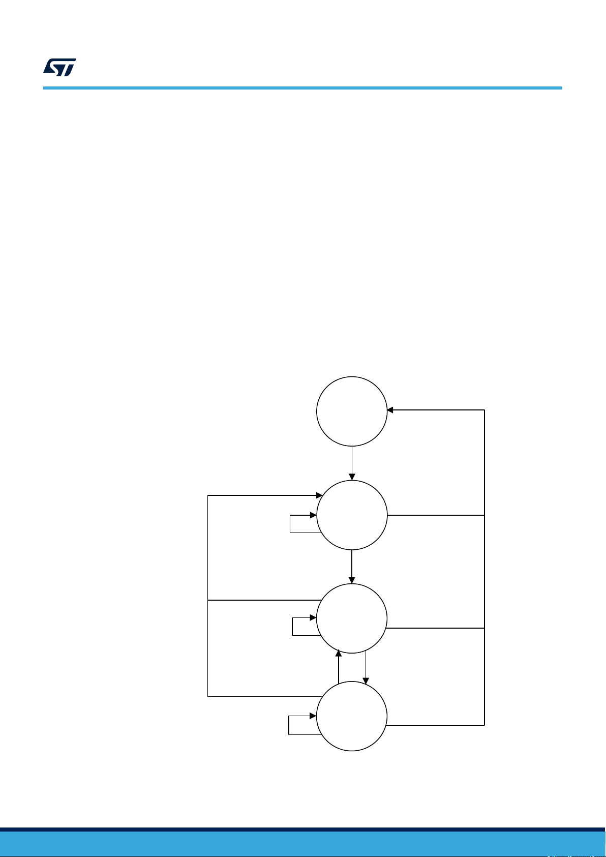
6.2.2 ST25TV02K/512 states referring to protocol
The ST25TV02K/512 can be in one of four states:
• Power-off
• Ready
• Quiet
• Selected
Transitions between these states are specified in Figure 9. state transition diagram and Table 31. response
depending on Request_flags.
Power-off state
Request
frame
Response
frame
t
2
t
1
t
2
DS12074 - Rev 11
The ST25TV02K/512 are in the power-off state when it does not receive enough energy from the VCD.
Ready state
The ST25TV02K/512 are in the Ready state when it receives enough energy from the VCD. When in the Ready
state, the ST25TV02K/512 answer any request where the Select_flag is not set.
Quiet state
When in the Quiet state, the ST25TV02K/512 answer any request with the Address_flag set, except for Inventory
requests.
Selected state
In the Selected state, the ST25TV02K/512 answer any request in all modes (see Section 6.2.3 Modes):
• Request in Select mode with the Select_flag set
• Request in Addressed mode if the UID matches
• Request in Non-Addressed mode as it is the mode for general requests
page 26/90
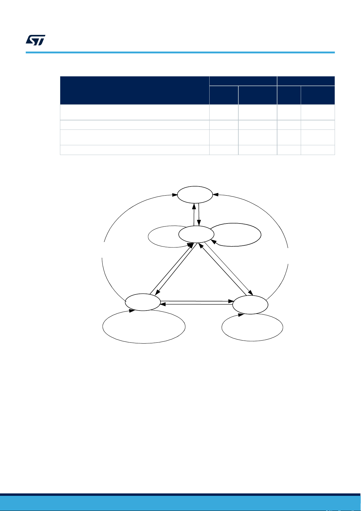
Table 31. response depending on Request_flags
Flags
ST25TV02K/512 in Ready or Selected state (Devices in Quiet state
do not answer)
ST25TV02K/512 in Selected state - X X -
ST25TV02K/512 in Ready, Quiet or Selected state (the device
which matches the UID)
Error (03h) or no response (command dependent) X - X -
Figure 9. state transition diagram
Power off
ST25TV02K ST25TV512
RF protocol description
Address_flag Select_flag
1
Addressed0Non addressed1Selected0Non selected
- X - X
X - - X
Out of field
after t
RF_OFF
Inventory
Out of RF field
after t
RF_OFF
Reset to ready
Quiet
Any other command where the
Address_Flag is set AND where
the Inventory_Flag is not set
Stay quiet(UID)
Select (UID)
1. The ST25TV02K/512 return to the Power Off state if the tag is out of the field for at least t
In RF field
Ready
Reset to ready where
Select_Flag is set or
Select with (# UID)
Stay quiet(UID)
Any other command
where Select_Flag
is not set
Select (UID)
Selected
Any other command
Out of RF field
after t
RF_OFF
RF_OFF
.
The intention of the state transition method is that only one ST25TV02K/512 should be in the Selected state at a
time.
When the Select_flag is set to 1, the request shall NOT contain a unique ID.
When the address_flag is set to 0, the request shall NOT contain a unique ID.
6.2.3 Modes
The term “mode” refers to the mechanism used in a request to specify the set of ST25TV02K/512 devices that
shall execute the request.
Addressed mode
When the Address_flag is set to 1 (Addressed mode), the request contains the Unique ID (UID) of the addressed
ST25TV02K/512.
DS12074 - Rev 11
page 27/90

Any ST25TV02K/512 that receive a request with the Address_flag set to 1 compares the received Unique ID to its
own. If it matches, then the ST25TV02K/512 execute the request (if possible) and return a response to the VCD
as specified in the command description.
If the UID does not match, then it remains silent.
Non-addressed mode (general request)
When the Address_flag is cleared to 0 (Non-Addressed mode), the request does not contain a UID.
Select mode
When the Select_flag is set to 1 (Select mode), the request does not contain a unique ID. The ST25TV02K/512 in
the Selected state that receives a request with the Select_flag set to 1 executes it and returns a response to the
VCD as specified in the command description.
Only the ST25TV02K/512 in the Selected state answers a request where the Select_flag is set to 1.
The system design ensures that only one ST25TV02K/512 can be in the Select state at a time.
6.2.4 Request format
The request consists of:
• an SOF
• flags
• a command code
• parameters and data
• a CRC
• an EOF
ST25TV02K ST25TV512
RF protocol description
SOF Request_flags Command code Parameters Data 2 byte CRC EOF
6.2.5 Request flags
In a request, the “flags” field specifies the actions to be performed by the ST25TV16K/64K and whether
corresponding fields are present or not.
The flags field consists of eight bits. Bit 3 (Inventory_flag) of the request flag defines the contents of the four
MSBs (bits 5 to 8). When bit 3 is reset (0), bits 5 to 8 define the ST25TV16K/64K selection criteria. When bit 3 is
set (1), bits 5 to 8 define the ST25TV16K/64K Inventory parameters.
Bit No Flag Level Description
Bit 1
Bit 2
Bit 3 Inventory_flag
Bit 4 Protocol_extension_flag
1. Subcarrier_flag refers to the ST25TV16K/64K-to-VCD communication.
2. Data_rate_flag refers to the ST25TV16K/64K-to-VCD communication.
Subcarrier_flag
Data_rate_flag
Table 32. General request format
Table 33. Definition of request flags 1 to 4
(1)
(2)
0 A single subcarrier frequency is used by the ST25TV16K/64K
1 Two subcarriers are used by the ST25TV16K/64K
0 Low data rate is used
1 High data rate is used
The meaning of flags 5 to 8 is described in Table 34. Request flags 5 to 8 when
0
inventory_flag, Bit 3 = 0
The meaning of flags 5 to 8 is described in Table 35. Request flags 5 to 8 when
1
inventory_flag, Bit 3 = 1
0 No Protocol format extension
1 Protocol format extension. Reserved for future use.
DS12074 - Rev 11
page 28/90

ST25TV02K ST25TV512
RF protocol description
Table 34. Request flags 5 to 8 when inventory_flag, Bit 3 = 0
Bit nb Flag Level Description
0 The request is executed by any ST25TV16K/64K according to the setting of Address_flag
Bit 5
Select flag
Bit 6 Address flag
Bit 7 Option flag
Bit 8 RFU 0 -
1. If the Select_flag is set to 1, the Address_flag is set to 0 and the UID field is not present in the request.
Bit nb Flag Level Description
Bit 5 AFI flag
Bit 6 Nb_slots flag
Bit 7 Option flag 0 -
Bit 8 RFU 0 -
(1)
1 The request is executed only by the ST25TV16K/64K in Selected state
The request is not addressed. UID field is not present. The request is executed by all
0
ST25TV16K/64Ks.
The request is addressed. UID field is present. The request is executed only by the
1
ST25TV16K/64K whose UID matches the UID specified in the request.
0 Option not activated.
1 Option activated.
Table 35. Request flags 5 to 8 when inventory_flag, Bit 3 = 1
0 AFI field is not present
1 AFI field is present
0 16 slots
1 1 slot
6.2.6 Response format
The response consists of:
• an SOF
• flags
• parameters and data
• a CRC
• an EOF
SOF Response_flags Parameters Data 2-byte CRC EOF
6.2.7 Response flags
In a response, the flags indicate how actions have been performed by the ST25TV02K/512 and whether
corresponding fields are present or not. The response flags consist of eight bits.
Table 36. General response format
DS12074 - Rev 11
page 29/90

Bit Nb Flag Level Description
Bit 1 Error_flag
Bit 2 RFU 0 -
Bit 3 RFU 0 -
Bit 4 RFU 0 -
Bit 5 RFU 0 -
Bit 6 RFU 0 -
Bit 7 RFU 0 -
Bit 8 RFU 0 -
6.2.8 Response and error code
If the Error_flag is set by the ST25TV02K/512 in the response, the Error code field is present and provides
information about the error that occurred.
Error codes not specified in Table 38. Response error code definition are reserved for future use.
ST25TV02K ST25TV512
Timing definition
Table 37. Definitions of response flags 1 to 8
0 No error
1 Error detected. Error code is in the “Error” field.
Error code Meaning
01h Command is not supported.
02h Command is not recognized (format error).
03h The option is not supported.
0Fh Error with no information given.
10h The specified block is not available.
11h The specified block is already locked and thus cannot be locked again.
12h The specified block is locked and its contents cannot be changed.
13h The specified block was not successfully programmed.
14h The specified block was not successfully locked.
15h The specified block is protected in read.
No response It might indicate illegal programming
6.3 Timing definition
t1: VICC response delay
Upon detection of the rising edge of the EOF received from the VCD, the ST25TV02K/512 wait for a t
before transmitting their response to a VCD request or switching to the next slot during an inventory process.
Values of t1 are given in Table 39. Timing values.
Table 38. Response error code definition
1nom
time
DS12074 - Rev 11
t2: VCD new request delay
t2 is the time after which the VCD may send an EOF to switch to the next slot when one or more ST25TV02K/512
responses have been received during an Inventory command. It starts from the reception of the EOF from the
ST25TV02K/512s.
The EOF sent by the VCD may be either 10% or 100% modulated regardless of the modulation index used for
transmitting the VCD request to the ST25TV02K/512.
page 30/90

ST25TV02K ST25TV512
RF commands
t2 is also the time after which the VCD may send a new request to the ST25TV02K/512, as described in
Figure 8. ST25TV02K/512 protocol timing.
Values of t2 are given in Table 39. Timing values.
t3: VCD new request delay when no response is received from the VICC
t3 is the time after which the VCD may send an EOF to switch to the next slot when no ST25TV02K/512 response
has been received.
The EOF sent by the VCD may be either 10% or 100% modulated regardless of the modulation index used for
transmitting the VCD request to the ST25TV02K/512.
From the time the VCD has generated the rising edge of an EOF:
• If this EOF is 100% modulated, the VCD waits for a time at least equal to t
sending a new EOF.
• If this EOF is 10% modulated, the VCD waits for a time at least equal to t
sending a new EOF.
Table 39. Timing values
for 100% modulation before
3min
for 10% modulation before
3min
Minimum (min) values
100% modulation 10% modulation
t
1
t
2
t
t
3
1max
4320 / fc = 318.6 µs
4192 / fc = 309.2 µs No t
(2)
(3)
+t
SOF
t
1max
(2)
+t
NRT
1. VCD request will not be interpreted during the first milliseconds following the field rising.
2. t
does not apply for write-alike requests. Timing conditions for write-alike requests are defined in the command
1max
description.
3. t
is the time taken by the ST25TV02K/512 to transmit an SOF to the VCD. t
SOF
data rate or Low data rate.
4. t
is the nominal response time of the ST25TV02K/512. t
NRT
sub-carrier modulation mode.
Note: The tolerance of specific timing is ±32 / fC.
6.4
RF commands
6.4.1 RF command code list
The ST25TV02K/512 support the following legacy and extended RF command set:
• Inventory, used to perform the anticollision sequence.
• Stay Quiet, used to put the ST25TV02K/512 in quiet mode, where it does not respond to any inventory
command.
• Select, used to select the ST25TV02K/512. After this command, the ST25TV02K/512 process all Read/
Write commands with Select_flag set.
• Reset To Ready, used to put the ST25TV02K/512 in the ready state.
• Read Single Block, used to output the 32 bit of the selected block and its locking status.
• Write Single Block, used to write and verify the new content for an update of a 32 bit block, provided that it
is not in a locked memory area.
• Read Multiple Blocks, used to read the selected 32 bit blocks and their locking statuses, and send back
their value.
• Write AFI, used to write the 8-bit value in the AFI register.
• Lock AFI, used to lock the AFI register.
• Write DSFID, used to write the 8-bit value in the DSFID register.
Nominal (nom) values Maximum (max) values
4352 / fc = 320.9 µs
nom
(4)
+t
2min
NRT
No t
nom
depends on the current data rate: High
SOF
depends on VCD to ST25TV02K/512 data rate and
4384 / fc = 323.3 µs
No t
No t
(1)
max
max
DS12074 - Rev 11
page 31/90

ST25TV02K ST25TV512
RF commands
• Lock DSFID, used to lock the DSFID register.
• Get System information, used to provide the standard system information values.
• Write Password, used to update the 32 or 64 bit of the selected areas or configuration password, but only
after presenting the current one.
• Lock Block, used to lock any user blocks.
• Present Password, enables the user to present a password to open a security session.
• Fast Read Single Block, used to output the 32 bits of the selected block and its locking status at doubled
data rate.
• Fast Read Multiple Blocks, used to output the selected blocks in one or multiple areas providing the
access rights are granted at doubled data rate.
• Get multiple block security status, used to send the security status of the selected block.
• Initiate, used to trigger the tag response to the Inventory Initiated sequence.
• Inventory Initiated, used to perform the anti-collision sequence triggered by the Initiate command.
• Fast Initiate, used to trigger the tag response to the Fast Inventory Initiated sequence (fast commands are
with higher data rate).
• Fast Inventory Initiated, used to perform the anti-collision sequence triggered by the Fast Initiate
command.
• Inventory read performs anti-collision sequence then output selected blocks
• Fast Inventory read performs inventory command then execute a read with data returned at doubled data
rate.
• Lock Kill, used to lock the Kill or untraceable mode password.
• Kill, used to definitively deactivate the tag.
• Set EAS, activates the EAS feature if the EAS feature is not locked. (Not protected by password or locked)
• Reset EAS, deactivates the EAS feature if the EAS feature is not locked. (not protected by password or
locked)
• Enable EAS, ST25TV02K/512 answer to this command only if EAS state is set. Response will include the
EAS Telegram (32 up to 256 bits depending on the EAS config)
• Write EAS ID writes a new EAS identifier Number. (Protected by configuration password).
• Write EAS CONFIG, used to configure the EAS telegram data length with 2bits 00 = 256 bits 01= 128 bits
10 = 64 bits 11= 32 bits (protected by configuration password).
• Lock EAS will lock EAS mode: (reset / set) and EAS ID and the EAS Telegram.
• Read Configuration used to read the counter values, the tamper detect status, and the number of Area.
• Write Configuration allows to enable the counter configuration, clear counter, set number of Area (1 or 2)
and their access rights, and lock the configuration block.
• Set Untraceable mode: sets the untraceable mode.
• Get Random Number: generates a 16 bit number.
DS12074 - Rev 11
page 32/90

6.4.2 Command codes list
The ST25TV02K/512 support the commands described in this section. Their codes are given in
Table 40. Command codes.
ST25TV02K ST25TV512
RF commands
Table 40. Command codes
Command code
standard
01h Section 6.4.4 Inventory A5h Section 6.4.26 Enable EAS
02h Section 6.4.5 Stay Quiet A6h Section 6.4.30 Kill
20h Section 6.4.6 Read Single Block A7h Section 6.4.28 Write EAS ID
21h Section 6.4.7 Write Single Block A8h Section 6.4.29 Write EAS CONFIG
22h Section 6.4.8 Lock block
23h Section 6.4.9 Read Multiple Blocks Section 6.4.20 Write Password
25h Section 6.4.10 Select B2h Section 6.4.32 Lock Kill
26h Section 6.4.11 Reset to Ready B3h Section 6.4.21 Present Password
27h Section 6.4.12 Write AFI B4h Section 6.4.40 Get Random Number
28h Section 6.4.13 Lock AFI BAh Section 6.4.39 Enable Untraceable mode
29h Section 6.4.14 Write DSFID C0h Section 6.4.22 Fast Read Single Block
2Ah Section 6.4.15 Lock DSFID C1h Section 6.4.33 Fast Inventory Initiated
2Bh Section 6.4.16 Get System info C2h Section 6.4.34 Fast Initiate
2Ch
A0h Section 6.4.18 Read Configuration D1h Section 6.4.35 Inventory Initiated
A1h Section 6.4.19 Write Configuration D2h Section 6.4.36 Initiate
A2h Section 6.4.24 Set EAS D3h Section 6.4.37 Inventory read
A3h Section 6.4.25 Reset EAS D4h Section 6.4.38 Fast inventory read
A4h Section 6.4.27 Lock EAS - -
Section 6.4.17 Get Multiple Block Security
Status
Function
Command code
custom
B1h
C3h Section 6.4.23 Fast Read Multiple Blocks
Section 6.4.31 Write Kill Password
Function
6.4.3 General Command Rules
In case of a valid command, the following paragraphs will describe the expected behavior for each command.
But in case of an invalid command, in a general manner, the ST25TV02K/512 will behave as follows:
1. If flag usage is incorrect, the error code 03h will be issued only if the right UID is used in the command,
otherwise no response will be issued.
2. The error code 02h will be issued if the custom command is used with the manufacturer code different from
the ST one
6.4.4 Inventory
Upon receiving the Inventory request, the ST25TV02K/512 run the anticollision sequence. The Inventory_flag is
set to 1. The meaning of flags 5 to 8 is shown in .
The request parameters:
• Request flags
• AFI if the AFI flag is set
• Mask length
• Mask value if mask length is different from 0
The ST25TV02K/512 do not generate any answer in case of error.
DS12074 - Rev 11
page 33/90

ST25TV02K ST25TV512
RF commands
Table 41. Inventory request format
Request SOF Request_flags Inventory Optional AFI Mask length Mask value CRC16 Request EOF
- 8 bits 01h 8 bits 8 bits 0 - 64 bits 16 bits -
The response contains:
• the flags
• the Unique ID
Table 42. Inventory response format
Response SOF Response_flags DSFID UID CRC16 Response EOF
- 8 bits 8 bits 64 bits 16 bits -
During an Inventory process, if the VCD does not receive an RF ST25TV02K/512 response, it waits for a time t
before sending an EOF to switch to the next slot. t3 starts from the rising edge of the request EOF sent by the
VCD.
• If the VCD sends a 100% modulated EOF, the minimum value of t3 is:
• t3min = 4384/fC (323.3µs) + t
SOF
• If the VCD sends a 10% modulated EOF, the minimum value of t3 is:
• t3min = 4384/fC (323.3µs) + t
NRT
+ t
2min
where:
• t
• t
t
NRT
is the time required by the ST25TV02K/512 to transmit an SOF to the VCD,
SOF
is the nominal response time of the ST25TV02K/512.
NRT
and t
are dependent on the ST25TV02K/512-to-VCD data rate and subcarrier modulation mode.
SOF
Note: In case of error, no response is sent by ST25TV02K/512.
6.4.5 Stay Quiet
On receiving the Stay Quiet command, the ST25TV02K/512 enter the Quiet state if no error occurs, and does
NOT send back a response. There is NO response to the Stay Quiet command even if an error occurs.
When in the Quiet state:
• the ST25TV02K/512 do not process any request if the Inventory_flag is set,
• the ST25TV02K/512 process any request with Address_flag set.
The ST25TV02K/512 exit the Quiet state when:
• it is reset (power off),
• receiving a Select request. It then goes to the Selected state,
• receiving a Reset to Ready request. It then goes to the Ready state.
Request parameters:
• request flags
• UID
3
DS12074 - Rev 11
Table 43. Stay Quiet request format
Request SOF Request flags Stay Quiet UID CRC16 Request EOF
- 8 bits 02h 64 bits 16 bits -
The Stay Quiet command must always be executed in Addressed mode (Select_flag is reset to 0 and
Address_flag is set to 1).
page 34/90

ST25TV02K ST25TV512
Figure 10. Stay Quiet frame exchange between VCD and ST25TV02K/512
RF commands
ST25TV02K/512
6.4.6 Read Single Block
On receiving the Read Single Block command, the ST25TV02K/512 read the requested block and sends back its
32-bit value in the response. The Option_flag is supported, when set response include the Block Security Status.
Block number is coded on 1 Byte.
Request SOF
- 8 bits 20h 64 bits 8 bits 16 bits -
1. The field is optional.
Request parameters:
• Request flags
• UID (optional)
• Block number
Request_flags Read Single Block
VCD
SOF
Stay Quiet
request
Table 44. Read Single Block request format
(1)
UID
Block number CRC16 Request EOF
EOF
Table 45. Read Single Block response format when Error_flag is NOT set
Response SOF
- 8 bits 8 bits 32 bits 16 bits -
1. The field is optional.
Response_flags
Block security status
(1)
Data CRC16 Response EOF
Response parameters:
• Block security status if Option_flag is set (see Table 46. Block security status)
• Four bytes of block data
Table 46. Block security status
b
Reserved for future use.
All at 0.
b
7
b
6
b
5
b
4
b
3
b
2
b
1
0
0: Current block not locked
1: Current block locked
Table 47. Read Single Block response format when Error_flag is set
Response SOF
- 8 bits 8 bits 16 bits -
Response_flags Error code CRC16 Response EOF
Response parameter:
DS12074 - Rev 11
page 35/90

• Error code as Error_flag is set
– 03h: command option not supported
– 10h: the specified block is not available
– 15h: the specified block is read-protected
Figure 11. Read Single Block frame exchange between VCD and ST25TV02K/512
ST25TV02K ST25TV512
RF commands
VCD
ST25TV02K/512
6.4.7 Write Single Block
On receiving the Write Single Block command, the ST25TV02K/512 write the data contained in the request to the
targeted block and reports whether the write operation was successful in the response. When the Option_flag is
set, wait for EOF to respond.
During the RF write cycle Wt, there should be no modulation (neither 100% nor 10%), otherwise the
ST25TV02K/512 may not program correctly the data into the memory. The Wt time is equal to t
302 µs (N is an integer).
Block number is coded on 1 Byte and only first 256 blocks of ST25TV02K/512 can be addressed using this
command.
Request SOF
- 8 bits 21h 64 bits 8 bits 32 bits 16 bits -
1. The field is optional.
Request_flags Write Single Block
SOF
Read Single Block
request
EOF
t
SOF
1
Table 48. Write Single Block request format
(1)
UID
Block number Data CRC16 Request EOF
Read Single Block
response
1nom
EOF
+ N ×
DS12074 - Rev 11
Request parameters:
• Request flags
• UID (optional)
• Block number
• Data
Table 49. Write Single Block response format when Error_flag is NOT set
Response SOF
- 8 bits 16 bits -
Response_flags CRC16 Response EOF
Response parameter:
• No parameter. The response is sent back after the writing cycle.
page 36/90

ST25TV02K ST25TV512
Table 50. Write Single Block response format when Error_flag is set
Response SOF Response_flags Error code CRC16 Response EOF
- 8 bits 8 bits 16 bits -
Response parameter:
• Error code as Error_flag is set
– 03h: command option not supported
– 10h: the specified block is not available
– 12h: the specified block is locked or protected and its contents cannot be changed
– 13h: the specified block was not successfully programmed
1. For more details, see Figure 5. Memory organization
Figure 12. Write Single Block frame exchange between VCD and ST25TV02K/512
(1)
RF commands
VCD
ST25TV02K/512
ST25TV02K/512
When the Option_flag is set, wait for EOF to respond.
Block number is coded on 1 Byte.
6.4.8 Lock block
On receiving the Lock block request, the ST25TV02K/512 lock the single block value permanently and protects its
content against new writing.
This command is applicable for all blocks of the user memory.
For a global protection of a area, update accordingly the AiSS bits in the system area. The Option_flag is
supported, when set wait for EOF to respond.
During the RF write cycle Wt, there should be no modulation (neither 100% nor 10%), otherwise the
ST25TV02K/512 may not lock correctly the single block value in memory. The Wt time is equal to t
× 302 µs (N is an integer).
SOF
Write Single
Block request
EOF
t
SOF
1
Write Single
Block response
W
t
EOF
SOF
Write sequence
when error
Write Single
Block response
1nom
EOF
+ N
Table 51. Locking scheme
Area access description
Area readable and writable 00b Lock possible
Area protected in write by password 01b
Area protected in read and write by password 10b Lock only possible if security session is open
DS12074 - Rev 11
Area x access rights
RW_PROTECTION_Ax [1:0]
Lock feature behavior
Lock only possible if security session is open
Error = 14h if Security Session is closed
page 37/90

ST25TV02K ST25TV512
RF commands
Area access description
Area protected in read.
Area disabled in write (no matter if security session
opened or not)
Request SOF
- 8 bits 22h 64 bits 8 bits 16 bits -
1. The field is optional.
Request_flags Lock block
Request parameter:
• Request Flags
• UID (optional)
• Block number (only value 00h or 01h) are allowed to protect the CCfile in case of NDEF usage.
Table 53. Lock block response format when Error_flag is NOT set
Response SOF Response_flags CRC16 Response EOF
- 8 bits 16 bits -
Area x access rights
RW_PROTECTION_Ax [1:0]
Error = 14h if Security Session is closed
11b
No lock is possible
Error = 11h (already locked)
Table 52. Lock block request format
(1)
UID
block number CRC16 Request EOF
Lock feature behavior
Response parameter:
• No parameter
Table 54. Lock single block response format when Error_flag is set
Response SOF
- 8 bits 8 bits 16 bits -
Response_flags Error code CRC16 Response EOF
Response parameter:
• Error code as Error_flag is set
– 03h: command option not supported
– 10h: block not available
– 11h: the specified block is already locked and thus cannot be locked again
– 14h: the specified block was not successfully locked
DS12074 - Rev 11
page 38/90

ST25TV02K ST25TV512
Figure 13. Lock single block frame exchange between VCD and ST25TV02K/512
RF commands
VCD
SOF
ST25TV02K/512
ST25TV02K/512
6.4.9 Read Multiple Blocks
When receiving the Read Multiple Block command, the ST25TV02K/512 read the selected blocks and sends back
their value in multiples of 32 bits in the response. The blocks are numbered from 00h to 3Fh in the request and
the value is minus one (-1) in the field. For example, if the “Number of blocks” field contains the value 06h, seven
blocks are read. When the Option_flag is set, the response returns the Block Security Status.
When a read multiple starts in an area with read access authorized and finishes in an area without read access
authorized, only the data available in the area with read access authorized is returned. When a read access starts
in an area with no read access authorized, an error is returned.
Block number is coded on 1 Byte.
Lock block
request
EOF
t
SOF
1
Lock block
response
W
t
EOF
SOF
Lock sequence
when error
Lock block
response
EOF
Table 55. Read Multiple Block request format
Request SOF Request_flags
- 8 bits 23h 64 bits 8 bits 8 bits 16 bits -
1. The field is optional.
Read Multiple
Block
UID
(1)
First block
number
Number of blocks CRC16 Request EOF
Request parameters:
• Request flags
• UID (optional)
• First block number
• Number of blocks
Table 56. Read Multiple Block response format when Error_flag is NOT set
Response SOF
- 8 bits
1. The field is optional.
2. Repeated as needed.
Response_
flags
Block security status
(2)
8 bits
(1)
Data CRC16 Response EOF
(2)
32 bits
16 bits -
Response parameters:
• Block security status if Option_flag is set (see Table 57. Block security status)
• N blocks of data
DS12074 - Rev 11
page 39/90

Table 57. Block security status
ST25TV02K ST25TV512
RF commands
b
Reserved for future use.
All at 0.
b
7
b
6
b
5
b
4
b
3
b
2
b
1
0
0: Current block not locked
1: Current block locked
Table 58. Read Multiple Block response format when Error_flag is set
Response SOF Response_flags Error code CRC16 Response EOF
- 8 bits 8 bits 16 bits -
Response parameter:
• Error code as Error_flag is set:
– 03h: command option is not supported
– 10h: the specified block is not available
– 15h: the specified block is read-protected
Figure 14. Read Multiple Block frame exchange between VCD and ST25TV02K/512
VCD
SOF
Read Multiple
Block request
EOF
ST25TV02K/512
6.4.10 Select
When receiving the Select command:
• If the UID is equal to its own UID, the ST25TV02K/512 enter or stay in the Selected state and sends a
response.
• If the UID does not match its own UID, the selected ST25TV02K/512 return to the Ready state and does not
send a response.
The ST25TV02K/512 answer an error code only if the UID is equal to its own UID. If not, no response is
generated. If an error occurs, the ST25TV02K/512 remain in its current state.
- 8 bits 25h 64 bits 16 bits -
Request parameter:
• Request flags
• UID
t
SOF
1
Read Multiple
Block response
EOF
Table 59. Select request format
Request SOF Request_flags Select UID CRC16 Request EOF
DS12074 - Rev 11
page 40/90

ST25TV02K ST25TV512
Table 60. Select Block response format when Error_flag is NOT set
Response SOF Response_flags CRC16 Response EOF
- 8 bits 16 bits -
Response parameter:
• No parameter
Table 61. Select response format when Error_flag is set
Response SOF Response_flags Error code CRC16 Response EOF
- 8 bits 8 bits 16 bits -
Response parameter:
• Error code as Error_flag is set:
– 03h: the option is not supported
Figure 15. Select frame exchange between VCD and ST25TV02K/512
RF commands
VCD
ST25TV02K/512
6.4.11 Reset to Ready
On receiving a Reset to Ready command, the ST25TV02K/512 return to the Ready state if no error occurs. In
the Addressed mode, the ST25TV02K/512 answer an error code only if the UID is equal to its own UID. If not, no
response is generated.
Request SOF Request_flags Reset to Ready
- 8 bits 26h 64 bits 16 bits -
1. The field is optional.
Request parameter:
• Request flags
• ID (optional)
SOF Select request
Table 62. Reset to Ready request format
EOF
t
SOF Select response EOF
1
(1)
UID
CRC16 Request EOF
DS12074 - Rev 11
Table 63. Reset to Ready response format when Error_flag is NOT set
Response SOF Response_flags CRC16 Response EOF
- 8 bits 16 bits -
Response parameter:
• No parameter
page 41/90

ST25TV02K ST25TV512
Table 64. Reset to ready response format when Error_flag is set
Response SOF Response_flags Error code CRC16 Response EOF
- 8 bits 8 bits 16 bits -
Response parameter:
• Error code as Error_flag is set:
– 03h: the option is not supported
Figure 16. Reset to Ready frame exchange between VCD and ST25TV02K/512
RF commands
ST25TV02K/512
6.4.12 Write AFI
On receiving the Write AFI request, the ST25TV02K/512 program the 8-bit AFI value to its memory. When the
Option_flag is set, wait for EOF to respond.
During the RF write cycle Wt, there should be no modulation (neither 100% nor 10%), otherwise the
ST25TV02K/512 may not write correctly the AFI value into the memory. The Wt time is equal to t
302 µs (N is an integer).
Request SOF Request_flags Write AFI
- 8 bits 27h 64 bits 8 bits 16 bits -
1. The field is optional.
Request parameter:
• Request flags
• UID (optional)
• AFI
VCD
SOF
Reset to Ready
request
EOF
t
Table 65. Write AFI request format
UID
1
SOF
(1)
AFI CRC16 Request EOF
Reset to Ready
response
1nom
EOF
+ N ×
DS12074 - Rev 11
Table 66. Write AFI response format when Error_flag is NOT set
Response SOF Response_flags CRC16 Response EOF
- 8 bits 16 bits -
Response parameter:
• No parameter
page 42/90

ST25TV02K ST25TV512
Table 67. Write AFI response format when Error_flag is set
RF commands
Response SOF
Response_
flags
Error code CRC16 Response EOF
- 8 bits 8 bits 16 bits -
Response parameter:
• Error code as Error_flag is set
– 03h: command option is not supported
– 0Fh: error with no information given
– 12h: the specified block is locked and its contents cannot be changed
– 13h: the specified block was not successfully programmed
Figure 17. Write AFI frame exchange between VCD and ST25TV02K/512
VCD
ST25TV02K/512
SOF
Write AFI
request
EOF
t
SOF
1
Write AFI
response
EOF
Write sequence
when error
ST25TV02K/512
6.4.13 Lock AFI
On receiving the Lock AFI request, the ST25TV02K/512 locks the AFI value permanently. When the Option_flag is
set, wait for EOF to respond.
During the RF write cycle Wt, there should be no modulation (neither 100% nor 10%), otherwise the
ST25TV02K/512 may not lock correctly the AFI value in memory. The Wt time is equal to t
µs.
Request SOF Request_flags Lock AFI
- 8 bits 28h 64 bits 16 bits -
1. The field is optional.
Request parameter:
• Request Flags
• UID (optional)
W
t
SOF EOF
Table 68. Lock AFI request format
UID
(1)
CRC16 Request EOF
Table 69. Lock AFI response format when Error_flag is NOT set
Write AFI
response
+ 18 × 302
1nom
DS12074 - Rev 11
Response SOF Response_flags CRC16 Response EOF
- 8 bits 16 bits -
page 43/90

ST25TV02K ST25TV512
Response parameter:
• No parameter
Table 70. Lock AFI response format when Error_flag is set
Response SOF Response_flags Error code CRC16 Response EOF
- 8 bits 8 bits 16 bits -
Response parameter:
• Error code as Error_flag is set
– 03h: command option is not supported
– 11h: the specified block is already locked and thus cannot be locked again
– 14h: the specified block was not successfully locked
Figure 18. Lock AFI frame exchange between VCD and ST25TV02K/512
RF commands
VCD
ST25TV02K/512
ST25TV02K/512
6.4.14 Write DSFID
On receiving the Write DSFID request, the ST25TV02K/512 program the 8-bit DSFID value to its memory. When
the Option_flag is set, wait for EOF to respond.
During the RF write cycle Wt, there should be no modulation (neither 100% nor 10%), otherwise the
ST25TV02K/512 may not write correctly the DSFID value in memory. The Wt time is equal to t
302 µs (N is an integer).
Request SOF Request_flags Write DSFID
- 8 bits 29h 64 bits 8 bits 16 bits -
1. The field is optional.
SOF
Lock AFI
request
EOF
t
SOF
1
Table 71. Write DSFID request format
W
UID
Lock AFI
response
t
(1)
EOF
SOF EOF
Lock sequence
when error
Lock AFI
response
+ N ×
1nom
DSFID CRC16 Request EOF
DS12074 - Rev 11
MS60271V1Request parameter:
• Request flags
• UID (optional)
• DSFID
page 44/90

ST25TV02K ST25TV512
Table 72. Write DSFID response format when Error_flag is NOT set
Response SOF Response_flags CRC16 Response EOF
- 8 bits 16 bits -
Response parameter:
• No parameter
Table 73. Write DSFID response format when Error_flag is set
Response SOF Response_flags Error code CRC16 Response EOF
- 8 bits 8 bits 16 bits -
Response parameter:
• Error code as Error_flag is set
– 03h: command option is not supported
– 12h: the specified block is locked and its contents cannot be changed
– 13h: the specified block was not successfully programmed
RF commands
VCD
ST25TV02K-512
ST25TV02K-512
6.4.15 Lock DSFID
On receiving the Lock DSFID request, the ST25TV02K/512 lock the DSFID value permanently. When the
Option_flag is set, wait for EOF to respond.
During the RF write cycle Wt, there should be no modulation (neither 100% nor 10%), otherwise the
ST25TV02K/512 may not lock correctly the DSFID value in memory. The Wt time is equal to t
(N is an integer).
Figure 19. Write DSFID frame exchange between VCD and ST25TV02K/512
SOF
Write DSFID
request
EOF
SOF
Write DSFID
response
W
t
EOF
SOF EOF
t
1
Write sequence
Write DSFID
response
1nom
when error
+ N × 302 µs
DS12074 - Rev 11
Table 74. Lock DSFID request format
Request SOF Request_flags Lock DSFID
- 8 bits 2Ah 64 bits 16 bits -
1. The field is optional.
UID
(1)
CRC16 Request EOF
Request parameter:
• Request flags
• UID (optional)
page 45/90

ST25TV02K ST25TV512
Table 75. Lock DSFID response format when Error_flag is NOT set
Response SOF Response_flags CRC16 Response EOF
- 8 bits 16 bits -
Response parameter:
• No parameter.
Table 76. Lock DSFID response format when Error_flag is set
Response SOF Response_flags Error code CRC16 Response EOF
- 8 bits 8 bits 16 bits -
Response parameter:
• Error code as Error_flag is set:
– 03h: command option is not supported
– 11h: the specified block is already locked and thus cannot be locked again
– 14h: the specified block was not successfully locked
RF commands
VCD
ST25TV02K/512
ST25TV02K/512
6.4.16 Get System info
When receiving the Get System Info command, the ST25TV02K/512 send back its information data in the
response. The Option_flag is not supported. The Get System Info can be issued in both Addressed and Non
Addressed modes.
Request SOF Request_flags Get System Info
- 8 bits 2Bh 64 bits 16 bits -
1. The field is optional.
Figure 20. Lock DSFID frame exchange between VCD and ST25TV02K/512
SOF
Lock DSFID
request
EOF
t
SOF
1
Lock DSFID
response
W
t
EOF
SOF EOF
Lock sequence
Lock DSFID
response
Table 77. Get System info request format
(1)
UID
CRC16 Request EOF
when error
DS12074 - Rev 11
Request parameter:
• Request flags
• UID (optional)
page 46/90

ST25TV02K ST25TV512
Table 78. Get System info response format Error_flag is NOT set
RF commands
Response SOF
- 00h 0Fh 64 bits 8 bits 8 bits 16 bits 48h 16 bits -
Response
flags
Information flags UID DSFID AFI VICC memory size IC ref. CRC16 Response EOF
Response parameters:
• Information flags set to 0Fh. DSFID, AFI, VICC memory size (16 bits), and IC reference fields are present.
• VICC memory size - possible values are:
– 033Fh for ST25TV02K
– 030Fh for ST25TV512
Note: The first byte is in both cases 03h. It corresponds to a block size of 4 bytes. The 2nd byte is 3Fh when ST25TV
has 64 blocks and 0Fh when ST25TV has 16 blocks.
• UID code on 64 bits
• DSFID value
• AFI value
• ST25TV02K/512 IC reference: the 8 bits are significant.
Table 79. Get System Info response format when Error_flag is set
Response SOF Response_flags Error code CRC16 Response EOF
- 01h 8 bits 16 bits -
Response parameter:
• Error code as Error_flag is set:
– 03h: Option not supported
Figure 21. Get System Info frame exchange between VCD and ST25TV02K/512
VCD
ST25TV02K/512
SOF
Get System info
request
6.4.17 Get Multiple Block Security Status
When receiving the Get Multiple Block Security Status command, the ST25TV02K/512 send back its security
status for each address block: 0 when block is writable else 1 when block is locked for writing. The blocks security
status are defined by the area security status (and the lock block status). The blocks are numbered from 00h up
to the maximum memory block number in the request, and the value is minus one (–1) in the field. For example,
a value of “06” in the “Number of blocks” field requests will return the security status of seven blocks. This
command does not respond an error if number of blocks overlap areas.
The number of blocks is coded on 1 Byte and only first 256 blocks of ST25TV02K/512 can be addressed using
this command.
EOF
t
SOF
1
Get System info
response
EOF
DS12074 - Rev 11
page 47/90

ST25TV02K ST25TV512
Table 80. Get Multiple Block Security Status request format
RF commands
Request SOF Request_flags
- 8 bits 2Ch 64 bits 8 bits 8 bits 16 bits -
1. The field is optional.
Get Multiple Block
Security Status
UID
(1)
First block
number
Number of
blocks
CRC16 Request EOF
Request parameter:
• Request flags
• UID (optional)
• First block number
• Number of blocks
Table 81. Get Multiple Block Security Status response format when Error_flag is NOT set
Response SOF Response_flags Block security status CRC16 Response EOF
- 8 bits
1. Repeated as needed.
8 bits
(1)
16 bits -
Response parameters:
• Block security status
Table 82. Block security status
b
Reserved for future use
All at 0
b
7
b
6
b
5
b
4
b
3
b
2
b
1
0
0: Current block not locked
1: Current block locked
Table 83. Get Multiple Block Security Status response format when Error_flag is set
Response SOF
- 8 bits 8 bits 16 bits -
Response_flags Error code CRC16 Response EOF
Response parameter:
• Error code as Error_flag is set:
– 03h: the option is not supported
– 10h: the specified block is not available
Figure 22. Get Multiple Block Security status frame exchange between VCD and ST25TV02K/512
VCD
ST25TV02K/512
SOF
Get Multiple Block
Security request
status
EOF
t
SOF
1
Security response
status
Get Multiple Block
EOF
DS12074 - Rev 11
page 48/90

ST25TV02K ST25TV512
6.4.18 Read Configuration
On receiving the Read Configuration command, the ST25TV02K/512 read the static system configuration register
at the Pointer address and sends back its 8-bit value in the response.
The Option_flag is not supported. The Inventory_flag must be set to 0.
Table 84. Read Configuration request format
Request SOF Request_flags Read Configuration IC Mfg code
- 8 bits A0h 02h 64 bits 8 bits 16 bits -
1. The field is optional.
Note: Please refer to Table 4. System configuration memory map accessible through write_cfg and read_cfg
commands for details on register addresses.
Request parameters:
• System configuration register pointer
• UID (optional)
Table 85. Read Configuration response format when Error_flag is NOT set
UID
(1)
Pointer CRC16 Request EOF
RF commands
Response SOF Response_flags Register value CRC16 Response EOF
- 8 bits
1. It depends on registers being accessed
8 or 16 bits
(1)
16 bits -
Response parameters:
• One or two bytes of data: system configuration register
Table 86. Read Configuration response format when Error_flag is set
Response SOF
- 8 bits 8 bits 16 bits -
Response_flags Error code CRC16 Response EOF
Response parameter:
• Error code as Error_flag is set
– 02h: command not recognized
– 03h: the option is not supported
– 10h: register not available
Figure 23. Read Configuration frame exchange between VCD and ST25TV02K/512
VCD
SOF
Read
Configuration
request
EOF
DS12074 - Rev 11
ST25TV02K/512
t
1
SOF
Read
Configuration
response
EOF
page 49/90

6.4.19 Write Configuration
The Write Configuration command is used to write system configuration register. The Write Configuration must
be preceded by a valid presentation of the configuration password (PWG_CFG) to open the RF configuration
security session.
On receiving the Write Configuration command, the ST25TV02K/512 write the data contained in the request to
the system configuration register at the Pointer address and reports whether the write operation was successful in
the response or not.
When the Option_flag is set, wait for EOF to respond. The Inventory_flag is not supported.
During the RF write cycle Wt, there should be no modulation (neither 100% nor 10%), otherwise the
ST25TV02K/512 may not program correctly the data into the Configuration byte. The Wt time is equal to t
N × 302 µs (N is an integer).
Table 87. Write Configuration request format
ST25TV02K ST25TV512
RF commands
+
1nom
Request SOF
- 8 bits A1h 02h 64 bits 8 bits 8 bits 16 bits -
1. The field is optional.
2. Before updating the register value, check the meaning of each bit in previous sections.
Request_
flags
Write Configuration IC Mfg code
UID
(1)
Pointer
Register Value
(2)
CRC16 Request EOF
Request parameters:
• Request flags
• Register pointer
• Register value
• UID (optional)
Table 88. Write Configuration response format when Error_flag is NOT set
Response SOF
- 8 bits 16 bits -
Response_flags CRC16 Response EOF
Note: Please refer to Table 4. System configuration memory map accessible through write_cfg and read_cfg
commands for details on register addresses.
Response parameter:
• No parameter. The response is sent back after the writing cycle.
DS12074 - Rev 11
Table 89. Write Configuration response format when Error_flag is set
Response SOF
- 8 bits 8 bits 16 bits -
Response_flags Error code CRC16 Response EOF
Response parameter:
• Error code as Error_flag is set:
– 02h: command not recognized
– 03h: command option is not supported
– 0Fh: error with no information given
– 10h: not available
– 12h: block already locked, content can't change
– 13h: the specified block was not successfully programmed
page 50/90

ST25TV02K ST25TV512
Figure 24. Write Configuration frame exchange between VCD and ST25TV02K/512
RF commands
VCD
ST25TV02K/512
ST25TV02K/512
6.4.20 Write Password
On receiving the Write Password command, the ST25TV02K/512 use the data contained in the request to write
the password and reports whether the operation was successful in the response. It is possible to modify a
Password value only after issuing a valid Present password command (of the same password number). When
the Option_flag is set, wait for EOF to respond. Refer to Section 5.2 Data protection for details on password
Management.
During the RF write cycle time, Wt, there must be no modulation at all (neither 100% nor 10%), otherwise the
ST25TV02K/512 may not correctly program the data into the memory.
The Wt time is equal to t
selected password is automatically activated. It is not required to present the new password value until the
ST25TV02K/512 power-down.
There is no anti-tearing mechanism during Write_Password command. Command must be applied with stable RF
field. Otherwise the write operation may not complete properly, and could imply a loss/corruption of password
content with no recovery capability.
It is recommended to use Write_Password command in Addressed or Selected modes, in order to improve the
system robustness. This allows to ensure that Password change is only applied to the concerned tag/UID.
SOF
1nom
Write
Configuration
request
EOF
t
SOF
1
Write
Configuration
response
W
t
EOF
SOF
Write Configuration
sequence when error
Write
Configuration
response
+ N × 302 µs (N is an integer). After a successful write, the new value of the
EOF
DS12074 - Rev 11
Table 90. Write Password request format
Request SOF Request_flags
- 8 bits B1h 02h 64 bits 8 bits 32 bits 16 bits -
1. The field is optional.
Write
password
IC Mfg code
UID
(1)
Password
number
Data CRC16 Request EOF
Request parameter:
• Request flags
• UID (optional)
• Password number:
– 00h = PWD_KILL or PWD_UNTRACEABLE
– 01h = PWD_1
– 02h = PWD_2
– 03h = PWD_CFG
– other = Error
• Data
page 51/90

ST25TV02K ST25TV512
Table 91. Write Password response format when Error_flag is NOT set
Response SOF Response_flags CRC16 Response EOF
- 8 bits 16 bits -
Response parameter:
• no parameter.
Table 92. Write Password response format when Error_flag is set
Response SOF Response_flags Error code CRC16 Response EOF
- 8 bits 8 bits 16 bits -
Response parameter:
• Error code as Error_flag is set:
– 02h: command not recognized
– 03h: command option not supported
– 10h: the password number is incorrect
– 12h: update right not granted, Present Password command not previously executed or password
locked
– 14h: block was not successfully programmed
RF commands
Figure 25. Write Password frame exchange between VCD and ST25TV02K/512
VCD
ST25TV02K/512
ST25TV02K/512
6.4.21 Present Password
On receiving the Present Password command, the ST25TV02K/512 compare the requested password with
the data contained in the request and report if the operation has been successful in the response. Refer to
Section 5.2 Data protection for details on password management. After a successful command, the security
session associated to the password is open as described in Section 5.2 Data protection.
SOF
Write
Password
request
EOF
t
SOF
1
Password
EOF
response
Write
Write sequence
when error
Write
W
t
SOF EOF
Password
response
DS12074 - Rev 11
Table 93. Present Password request format
Request
SOF
- 8 bits B3h 02h 64 bits 8 bits 32 or 64 bits 16 bits -
1. The field is optional.
Request_flags
Present
Password
IC Mfg
code
UID
(1)
Password
number
Password CRC16
Request parameters:
Request
EOF
page 52/90

ST25TV02K ST25TV512
RF commands
• Request flags
• UID (optional)
• Password number (00h = Password KILL or UNTRACEABLE, 0x01 = PWD_A1, 0x02 = PWD_A2, 0x03 =
PWD_CFG, other = Error)
• Password is 32-bit wide for all passwords, except for Area 1 if MEM_ORG = 1b1 (ST25TV02K/512
configured in two areas), when the password is 64-bit wide.
Table 94. Present Password response format when Error_flag is NOT set
Response SOF Response_flags CRC16 Response EOF
- 8 bits 16 bits -
Response parameter:
• No parameter. The response is sent back after the write cycle.
Table 95. Present Password response format when Error_flag is set
Response SOF Response_flags Error code CRC16 Response EOF
- 8 bits 8 bits 16 bits -
Response parameter:
• Error code as Error_flag is set:
– 02h: command not recognized
– 03h: command option not supported
– 0Fh: the present password is incorrect
– 10h: the password number is incorrect
Figure 26. Present Password frame exchange between VCD and ST25TV02K/512
VCD
ST25TV02K/512
ST25TV02K/512
SOF
Present
Password
request
EOF
t
PDW_FAIL
Present
Password
response
EOF
SOF
Good password
Present
Password
response
EOF
Wrong password
t
SOF
1
Present password command specificity
The passwords must be presented encrypted as explained in AN5103.
6.4.22 Fast Read Single Block
On receiving the Fast Read Single Block command, the ST25TV02K/512 read the requested block and sends
back its 32-bit value in the response. When the Option_flag is set, the response includes the Block Security
Status. The data rate of the response is multiplied by 2.
DS12074 - Rev 11
page 53/90

ST25TV02K ST25TV512
The subcarrier_flag should be set to 0, otherwise the ST25TV02K/512 answer with an error code.
Block number is coded on 1 Byte.
Table 96. Fast Read Single Block request format
(1)
(1)
UID
Block number CRC16 Request EOF
Data CRC16 Response EOF
Request SOF Request_flags Fast Read Single Block IC Mfg code
- 8 bits C0h 02h 64 bits 8 bits 16 bits -
1. The field is optional.
Request parameters:
• Request flags
• UID (optional)
• Block number
Table 97. Fast Read Single Block response format when Error_flag is NOT set
Response SOF
- 8 bits 8 bits 32 bits 16 bits -
1. The field is optional.
Response_flags
Block security status
RF commands
Response parameters:
• Block security status if Option_flag is set (see Table 98. Block security status)
• Four bytes of block data
Table 98. Block security status
b
Reserved for future use
All at 0
b
7
b
6
b
5
b
4
b
3
b
2
b
1
0
0: Current Block not locked
1: Current Block locked
Table 99. Fast Read Single Block response format when Error_flag is set
Response SOF
- 8 bits 8 bits 16 bits -
Response_flags Error code CRC16 Response EOF
Response parameter:
• Error code as Error_flag is set:
– 02h: command not recognized
– 03h: command option not supported
– 10h: the specified block is not available
– 15h: the specified block is read-protected
DS12074 - Rev 11
page 54/90

ST25TV02K ST25TV512
RF commands
Figure 27. Fast Read Single Block frame exchange between VCD and ST25TV02K/512
VCD
SOF
ST25TV02K/512
6.4.23 Fast Read Multiple Blocks
On receiving the Fast Read Multiple Blocks command, the ST25TV02K/512 read the selected blocks and sends
back their value in multiples of 32 bits in the response. The blocks are numbered from 00h up to the last block of
user memory in the request, and the value is minus one (-1) in the field. For example, if the “Number of blocks”
field contains the value 06h, seven blocks are read. If the number of blocks overlaps area, the ST25TV02K/512
return only the blocks that are readable assuming reading starts from an Area that is readable, and stops when
reaching an Area that is not readable.
When the Option_flag is set, the response includes the Block Security Status. The data rate of the response is
multiplied by 2.
The subcarrier_flag should be set to 0, otherwise the ST25TV02K/512 answer with an error code.
Block number is coded on 1 Byte.
Fast Read
Single Block
EOF
request
t
SOF
1
Table 100. Fast Read Multiple Block request format
Fast Read
Single Block
response
EOF
Request
SOF
- 8 bits C3h 02h 64 bits 8 bits 8 bits 16 bits -
1. The field is optional.
Request_flags
Fast Read
Multiple Block
IC Mfg
code
UID
(1)
First block
number
Number of
blocks
CRC16
Request parameters:
• Request flag
• UID (Optional)
• First block number
• Number of blocks
Table 101. Fast Read Multiple Block response format when Error_flag is NOT set
Response SOF
- 8 bits
1. The field is optional.
2. Repeated as needed.
Response_flags
Block security status
(2)
8 bits
(1)
Data CRC16 Response EOF
(2)
32 bits
16 bits -
Response parameters:
• Block security status if Option_flag is set (see Table 102. Block security status if Option_flag is set)
• N block of data
Request
EOF
DS12074 - Rev 11
Table 102. Block security status if Option_flag is set
b
7
b
6
b
5
b
4
b
3
b
2
b
1
b
0
page 55/90

ST25TV02K ST25TV512
RF commands
Reserved for future
use All at 0
0: Current not locked
1: Current locked
Table 103. Fast Read Multiple Block response format when Error_flag is set
Response SOF Response_flags Error code CRC16 Response EOF
- 8 bits 8 bits 16 bits -
Response parameter:
• Error code as Error_flag is set:
– 02h: command not recognized
– 03h: the option is not supported
– 10h: block address not available
– 15h: block read-protected
Figure 28. Fast Read Multiple Block frame exchange between VCD and ST25TV02K/512
VCD
SOF
Fast Read
Multiple block
request
EOF
ST25TV02K/512
6.4.24 Set EAS
The set command will activate the function if the EAS feature is not locked nor protected by the configuration
password.
If the EAS mode is locked, the Set EAS command will be ignored, and the ST25TV02K/512 respond with an error.
When the EAS mode is not locked:
• If the EAS mode is not protected by password, the Set EAS command will set the EAS mode.
• If the EAS mode is password protected, the configuration password has to be first transmitted with the
PRESENT PASSWORD command. Then the set EAS command can be executed, and will set the EAS
mode.
• If the EAS mode is password protected, but the PRESENT PASSWORD has not been transmitted before or
not successful, the set EAS command is not executed and the ST25TV02K/512 respond with an error.
Request SOF
- 8 bits A2h 02h 64 bits 16 bits -
1. The field is optional.
t
1
Table 104. Set EAS request format
Request_flags Set EAS IC Mfg code
SOF
UID
Fast Read
Multiple block
response
(1)
EOF
CRC16 request EOF
DS12074 - Rev 11
Request parameters:
• Request flags
• UID (optional)
page 56/90

ST25TV02K ST25TV512
RF commands
Table 105. Set EAS response when Error_flag is NOT set
Response SOF Response flags CRC16 request EOF
- 8 bits 16 bits -
Response parameter:
• No parameter
Table 106. Set EAS response when Error_flag is set
Response SOF Response flags Error code CRC16 request EOF
- 8 bits 8 bits 16 bits -
Response parameter:
• Error code as Error_flag is set
– 03h: command option is not supported
– 12h: the EAS configuration cannot be changed as eith the security session is closed, or locked
– 13h: the EAS configuration was not successfully programmed
6.4.25 Reset EAS
The Reset EAS command is used to deactivate the EAS if the EAS feature is not locked nor protected by the
configuration password.
If the EAS mode is locked, the Reset EAS command will be ignored, and the ST25TV02K/512 respond with an
error.
When the EAS mode is not locked:
• If the EAS mode is not protected by password, the Reset EAS command will clear the EAS mode.
• If the EAS mode is password protected the configuration password has to be first transmitted with the
PRESENT PASSWORD command. Then the reset EAS command can be executed, and will clear the EAS
mode
• If the EAS mode is password protected, but the PRESENT PASSWORD has not been transmitted before or
not successful, the reset EAS command is not executed and the ST25TV02K/512 respond with an error
Request SOF
- 8 bits A3h 02h 64 bits 16 bits -
1. The field is optional.
Request parameters:
• Request flags
• UID (optionfal)
Table 107. Reset EAS request format
Request_flags Reset EAS IC Mfg code
UID
(1)
CRC16 request EOF
DS12074 - Rev 11
Table 108. Reset EAS format when Error_flag is NOT set
Response SOF
- 8 bits 16 bits -
Response_flags CRC16 request EOF
Response parameter:
• No parameter
page 57/90

Response SOF Response_flags CRC16 request EOF
- 8 bits 16 bits -
Response parameter:
• • Error code as Error_flag is set
– 03h: command option is not supported
– 12h: the EAS configuration cannot be changed as eith the security session is closed, or locked
– 13h: the EAS configuration was not successfully programmed
6.4.26 Enable EAS
ST25TV02K/512 will respond with the Telegram or the EAS ID contents when the Enable EAS command is
received depending on the option flag bit, and the EAS ID in the command
• If the option flag of the Enable EAS command is set to “0”, the ST25TV02K/512 expect that the reader does
not transmit the EAS ID Mask length and EAS ID value. The ST25TV02K/512 will respond with the EAS
Telegram
• If the option flag of the EAS Enable command is set to “1”, the ST25TV02K/512 expect the reader transmits
the EAS ID Mask length and EAS ID value, and will present the EAS ID or the Telegram depending on the
mask length value
– If Mask == 00h, the ST25TV02K/512 return its 16-bit EAS ID
– If Mask != 00h, the Mask identifies how many bits of the EAS ID are valid. Only EAS Mask length
values 0, 8 and 16 are supported. The ST25TV02K/512 will compare the EAS ID value of the reader’s
command with its own EAS ID. If they match, the ST25TV02K/512 return its EAS telegram. If they
mismatch the ST25TV02K/512 will ignore the command. This is a selective EAS.
The enable command is answered without error by ST25TV02K/512 only if the Set command has been executed
before. Otherwise, the ST25TV02K/512 remain silent.
The EAS telegram is returned starting with the LSB, which is transmitted first, read from left to right.
ST25TV02K ST25TV512
RF commands
Table 109. Reset EAS format when Error_flag is set
Table 110. Enable EAS request format
Request SOF Request_flags Enable EAS
- 8 bits A5h 02h 64 bits 8 bits 0, 8 or 16 bits 16 bits -
IC Mfg
code
UID
(1)
EAS ID Mask
(2)
EAD ID
(2)
1. The field is optional.
2. Only if the option flag of the EAS Enable command is set to “1”
CRC16
request
Request parameters:
• Request flags
• UID (optional)
Table 111. Enable EAS response format when Error_flag is NOT set
Response SOF
- 8 bits 2 up to 256 bits 16 bits 16 bits -
1. Available for the proper Option_flag and Mask settings.
Response_flags
EAS Telegram
(1)
EAS ID
(1)
CRC16 request EOF
Response parameter:
• No parameter
EOF
DS12074 - Rev 11
page 58/90

6.4.27 Lock EAS
The EAS ID, the Telegram, the EAS telegram and EAS mode (reset/set) configuration can be locked definitively
with the lock_EAS command. It is not possible to unlock these EAS states once locked (even if presenting the
configuration password).
If the EAS configuration is password protected, the configuration password has to be first presented for the lock to
be performed
The lock_single_block command is not authorized on the EAS telegram blocks and will return an error.
Request SOF Request_flags Lock EAS IC Mfg code
- 8 bits A4h 02h 64 bits 16 bits -
1. The field is optional.
Request parameters:
• Request flags
• UID (optional)
ST25TV02K ST25TV512
Table 112. Lock EAS request format
(1)
UID
Table 113. Lock EAS response format when Error_flag is NOT set
CRC16 request EOF
RF commands
Response SOF Response_flags CRC16 request EOF
- 8 bits 16 bits -
Response parameter:
• No parameter
Response SOF
- 8 bits 8 bits 16 bits -
Response parameter:
• Error code as Error_flag is set
– 03h: command option is not supported
– 11h: the configuration is already locked and thus cannot be locked again
– 12h: the configuration cannot be changed as either the security session is closed, or locked
– 13h: the configuration could not be successfully programmed
6.4.28 Write EAS ID
This command writes a new EAS ID (16 bits words stored in the configuration area)
If the EAS parameters are protected by the configuration password then the command can be executed only if the
configuration password has been successfully presented earlier in the same session.
If EAS is locked, the command is not authorized and the ST25TV02K/512 will return an error.
Table 114. Lock EAS response format when Error_flag is set
Response_flags Error code CRC16 EOF
DS12074 - Rev 11
Table 115. Write EAS ID request format
Request SOF
- 8 bits A7h 02h 64 bits 16 bits 16 bits -
1. The field is optional.
Request_flags Write EAS ID IC Mfg code
UID
(1)
EAS ID CRC16 request EOF
Request parameters:
page 59/90

ST25TV02K ST25TV512
RF commands
• Request flags
• UID (optional)
• EAS ID
Table 116. Write EAS response format when Error_flag is NOT set
Response SOF Response_flags CRC16 request EOF
- 8 bits 16 bits -
Response parameter:
• No parameter
Table 117. Write EAS response format when Error_flag is set
Response SOF Response_flags Error code CRC16 request EOF
- 8 bits 8 bits 16 bits -
Response parameter:
• Error code as Error_flag is set
– 03h: command option is not supported
– 12h: the EAS configuration cannot be changed as either the security session is closed, or locked
– 13h: the EAS configuration could not be programmed successfully
6.4.29 Write EAS CONFIG
This command writes the telegram length in the EAS configuration register in the 2 following bits. It is protected by
the configuration password if EAS_SEC = ‘1’
If EAS is locked, the command is not authorized and the ST25TV02K/512 will return an error.
bit 1 bit 0 EAS telegram length Location
0 0 256 bits payload EAS block 1 to 8
0 1 128 bits payload EAS block 1 to 4
1 0 64 bits payload EAS block 1to 2
1 1 32 bits payload EAS block 1
Note: The bits from 7 to 2 are set to 0.
Request SOF
- 8 bits A8h 02h 64 bits 8 bits 16 bits -
1. The field is optional.
Request parameters:
• Request flags
• UID (optional)
• EAS CONFIG
Request_flags Write EAS CONFIG IC Mfg code
Table 118. EAS configuration bits
Table 119. Write EAS CONFIG request format
(1)
UID
EAS configuration CRC16 request EOF
DS12074 - Rev 11
page 60/90

ST25TV02K ST25TV512
RF commands
Table 120. Write EAS CONFIG response format when Error_flag is NOT set
Response SOF Response_flags CRC16 request EOF
- 8 bits 16 bits -
Response parameter:
• No parameter
Table 121. Write EAS CONFIG response format when Error_flag is set
Response SOF Response_flags Error code CRC16 request EOF
- 8 bits 8 bits 16 bits -
Response parameter:
• Error code as Error_flag is set
– 03h: command option is not supported.
– 12h: the EAS configuration cannot be changed as either the security session is closed, or is locked.
– 13h: the EAS configuration is not successfully programmed
6.4.30 Kill
When ST25TV02K/512 receive the Kill command request with the proper parameters, the ST25TV02K/512 enter
the Kill mute mode, and ST25TV02K/512 are killed. It can't be read or written and stays mute to any request. Kill
mute mode is definitive.
On receiving the Kill command, in the Addressed mode only, the ST25TV02K/512 compare the kill code (sent
unencrypted) with the data contained in the request and reports whether the operation was successful in the
response.
The Option_flag is supported. If the command is received in the Non Addressed or the Selected mode, the
ST25TV02K/512 return an error response.
During the comparison cycle equal to tW, there should be no modulation (neither 100% nor 10%). Otherwise,
the ST25TV02K/512 may not match the kill code correctly. The tW time is equal to t1nom +18 x 302 μs. After a
successful Kill command, the ST25TV02K/512 are deactivated and does not interpret any other command.
Request SOF Request_flags Kill IC Mfg code UID Kill password Kill code CRC16 request EOF
- 8 bits A6h 02h 64 bits 00h 32 bits 16 bits -
Request parameters:
• Request flags
• UID (mandatory)
• Kill password
Table 122. Kill request format
DS12074 - Rev 11
Table 123. Kill response format when Error_flag is NOT set
Response SOF
- 8 bits 16 bits -
Response_flags CRC16 request EOF
Response parameter:
• N/A
page 61/90

Response SOF Response_flags Error code CRC16 request EOF
- 8 bits 8 bits 16 bits -
Response parameter:
• Error code as Error_flag is set
– 03h: command option is not supported
– 0Fh: error with no information given
– 10h: block address not available
– 14h: Kill mute mode could not be locked successfully
6.4.31 Write Kill Password
On receiving the Write Kill command, the ST25TV02K/512 write the kill password (sent unencrypted) with the data
contained in the request and reports whether the operation was successful in the response.
The Option_flag is supported. After a successful write, the kill code must be locked by a Lock Kill command to
activate the protection.
During the write cycle tW, there should be no modulation (neither 100% nor 10%).
Otherwise, the ST25TV02K/512 may not correctly program the data to the memory. The tW time is equal to t1nom
+18 x 302 μs.
ST25TV02K ST25TV512
RF commands
Table 124. Kill response format when Error_flag is set
Table 125. Write Kill Password request format
Request
SOF
- 8 bits B1h 02h 64 bits 00h 32 bits 16 bits -
1. The field is optional.
Request_flags
Write Kill
Password
IC Mfg
code
(1)
Kill access Kill password
UID
CRC16
request
Request parameters:
• Request flags
• UID (optional)
• Kill password
Table 126. Write Kill response format when Error_flag is NOT set
Response SOF
- 8 bits 16 bits -
Response_flags CRC16 request EOF
Response parameter:
• N/A
Table 127. Write Kill response format when Error_flag is set
Response SOF
- 8 bits 8 bits 16 bits -
Response_flags Error code CRC16 request EOF
EOF
DS12074 - Rev 11
Response parameter:
page 62/90

• Error code as Error_flag is set
– 03h: command option is not supported
– 10h: block address not available
– 12h: the Kill access code is locked
– 13h: the Kill access code was not successfully programmed
6.4.32 Lock Kill
On receiving the Lock Kill command, the ST25TV02K/512 lock the Kill password permanently.
The Option_flag is supported.
During the write cycle tW, there should be no modulation (neither 100% nor 10%).
Otherwise, the ST25TV may not lock the memory block correctly. The tW time is equal to
t
+ 18 x 302 μs.
1nom
ST25TV02K ST25TV512
RF commands
Table 128. Lock Kill request format
Request
SOF
- 8 bits B2h 02h 64 bits 00h 01h 16 bits -
1. The field is optional.
Request_fla
gs
Lock Kill
IC Mfg
code
UID
(1)
Kill access
Protect
status
CRC16
request
Request parameters:
• Request flags
• UID (optional)
• Kill access code
• Protection status
Table 129. Lock Kill response format when Error_flag is NOT set
Response SOF
- 8 bits 16 bits -
Response_flags CRC16 request EOF
Response parameter:
• No response: under unauthorized request flags and request parameters
Table 130. Lock Kill response format when Error_flag is set
Response SOF
- 8 bits 8 bits 16 bits -
Response_flags Error code CRC16 request EOF
EOF
Response parameter:
• Error code as Error_flag is set
– 03h: command option is not supported
– 0Fh: error with no information given
– 10h: access code not available
– 11h: the configuration is already locked and thus cannot be locked again
– 14h: Kill mute mode could not be locked successfully
6.4.33 Fast Inventory Initiated
Before receiving the Fast Inventory Initiated command, the ST25TV02K/512 must have received an Initiate or a
Fast Initiate command in order to set the Initiate_flag. If not, the ST25TV does not answer to the Fast Inventory
Initiated command.
DS12074 - Rev 11
page 63/90

ST25TV02K ST25TV512
On receiving the Fast Inventory Initiated request, the ST25TV02K/512 run the anticollision sequence.
The Inventory_flag must be set to 1. The data rate of the response is multiplied by 2.
The ST25TV02K/512 do not generate any answer if an error occurs.
Table 131. Fast Inventory Initiated request format
RF commands
Request SOF Request_flags
- 8 bits C1h 02h 8 bits 8 bits 0 -64 bits 16 bits -
1. The field is optional.
Fast Inventory
Initiated
IC Mfg code
Request parameters:
• Request flags
• Fast Inventory Initiated command code
• AFI if the AFI flag is set
• mask length
• mask value
Table 132. Fast Inventory Initiated response format when Error_flag is NOT set
Response SOF Response_flags DSFID UID CRC16 request EOF
- 8 bits 8 bits 64 bits 16 bits -
Response parameter:
• DSFID
• Unique ID
During an Inventory process, if the VCD does not receive an RF ST25TV02K/512 response, it waits t3 time before
sending an EOF to switch to the next slot. t3 starts from the rising edge of the request EOF sent by the VCD.
• If the VCD sends a 100% modulated EOF, the minimum value of t3 is:
– t
= 4384 / fC (323.3 μs) + t
3min
SOF
• If the VCD sends a 10% modulated EOF, the minimum value of t3 is:
– t
= 4384/fC (323.3 μs) + t
3min
NRT
where:
• t
• t
• t
is the time required by the ST25TV02K/512 to transmit an SOF to the VCD.
SOF
is the nominal response time of the ST25TV02K/512.
NRT
NRT
and t
are dependent on the ST25TV02K/512-to-VCD data rate and subcarrier modulation mode.
SOF
Note: In case of error, no response is sent by ST25TV02K/512.
(1)
Mask length Mask value
AFI
CRC16
request
EOF
6.4.34 Fast Initiate
On receiving the Fast Initiate command, the ST25TV02K/512 set the internal Initiate_flag and sends back a
response. The command has to be issued in the Non Addressed mode only (Select_flag is reset to 0 and
Address_flag is reset to 0). If an error occurs, the ST25TV02K/512 do not generate any answer. The Initiate_flag
is reset after a power off of the ST25TV02K/512. The data rate of the response is multiplied by 2.
Request SOF Request_flags Fast initiate IC Mfg code CRC16 request EOF
- 8 bits C2h 02h 16 bits -
Request parameters:
DS12074 - Rev 11
Table 133. Fast initiate request format
page 64/90

• Request flags
• Fast initiate command code
Response SOF Response_flags DSFID UID CRC16 request EOF
- 8 bits 8 bits 64 bits 16 bits -
Response parameter:
• DSFID
• Unique ID
6.4.35 Inventory Initiated
Before receiving Inventory Initiated command, the ST25TV02K/512 must have received an Initiate or a Fast
Initiate command in order to set the Initiate_flag. If not, the ST25TV02K/512 do not answer to the Inventory
Initiated command.
On receiving the Inventory Initiated request, the ST25TV02K/512 run the anticollision sequence.
The Inventory_flag must be set to 1.
The ST25TV02K/512 do not generate any answer if an error occurs.
The request contains:
ST25TV02K ST25TV512
RF commands
Table 134. Fast initiate response format when Error_flag is NOT set
Table 135. Inventory Initiated request format
Request SOF Request_flags
- 8 bits D1h 02h 8 bits 8 bits 0 -64 bits 16 bits -
1. The field is optional.
Inventory
Initiated
IC Mfg code
(1)
Mask length Mask value CRC16 request EOF
AFI
Request parameters:
• Request flags
• Inventory Initiated command code
• AFI if the AFI flag is set
• Mask length
• Mask value
Table 136. Inventory Initiated response format when Error_flag is NOT set
Response SOF
- 8 bits 8 bits 64 bits 16 bits -
Response_flags DSFID UID CRC16 request EOF
Response parameter:
• DSFID
• Unique ID
During an Inventory process, if the VCD does not receive an RF ST25TV response, it waits t3 time before sending
an EOF to switch to the next slot. t3 starts from the rising edge of the request EOF sent by the VCD.
• If the VCD sends a 100% modulated EOF, the minimum value of t3 is:
t
= 4384/fC (323.3 μs) + t
3min
SOF
• If the VCD sends a 10% modulated EOF, the minimum value of t3 is:
t
= 4384/fC (323.3 μs) + t
3min
NRT
where:
DS12074 - Rev 11
page 65/90

ST25TV02K ST25TV512
RF commands
• t
SOF
• t
NRT
t
and t
NRT
mode.
6.4.36 Initiate
On receiving the Initiate command, the ST25TV02K/512 set the internal Initiate_flag and sends back a response.
The command has to be issued in the Non Addressed mode only (Select_flag is reset to 0 and Address_flag is
reset to 0). If an error occurs, the ST25TV02K/512 do not generate any answer.
The Initiate_flag is reset after a power off of the ST25TV02K/512.
The request contains:
Request SOF Request_flags Initiate IC Mfg code CRC16 request EOF
- 8 bits D2h 02h 16 bits -
Request parameters:
• Request flags
• Initiated command code
is the time required by the ST25TV02K/512 to transmit an SOF to the VCD
is the nominal response time of the ST25TV02K/512
are dependent on the ST25TV02K/512-to-VCD data rate and subcarrier modulation
SOF
Table 137. Initiate request format
Table 138. Initiate response format when Error_flag is NOT set
Response SOF Response_flags DSFID UID CRC16 request EOF
- 8 bits 8 bits 64 bits 16 bits -
Response parameter:
• DSFID
• Unique ID
6.4.37 Inventory read
The Inventory read performs an inventory followed by a multiple block read.
If an error is detected, no matter if on the inventory or the read part, ST25TV02K/512 do not answer.
The request contains:
Table 139. Inventory read request format
Request
SOF
- 8 bits D3h 02h 8 bits 8 bits 0 -64 bits 8 bits 8 bits 16 bits -
1. The field is optional.
Request_flags
Inventory
Read
IC Mfg
code
AFI
(1)
Mask
length
Mask
value
Request parameters:
• Request flags. (The Nb_slots flag (bit 6) of the Request flags bits 5 to 8 described in , must be set to 1 for 1
slot inventory. 16 slot inventory is not supported in the inventory read command.
• Inventory read command code
• AFI if the AFI flag is set
• Mask length
• Mask value
• First block number
First
block
number
Number
of blocks
CRC16
request
EOF
DS12074 - Rev 11
page 66/90

ST25TV02K ST25TV512
RF commands
• Number of blocks
Table 140. Inventory read response format
Response SOF Request_flags DSFID UID
- 8 bits 8 bits 64 bits
Block security status
(2)
8 bits
1. The field is optional.
2. The group of Block security status (if any), and its data are repeated if needed, for up to the number of blocks requested.
Request parameter:
• Unique ID
• Block security status if Option_flag is set (see Table 46. Block security status)
• N blocks of data
Table 141. Block security status
(1)
Data CRC16 request EOF
(2)
32 bits
16 bits -
b
b
7
b
6
5
Reserved for future use.
All at 0.
During an Inventory Read process, if the VCD does not receive an RF ST25TV02K/512 response, it waits t3 time
before sending an EOF to switch to the next slot. t3 starts from the rising edge of the request EOF sent by the
VCD.
• If the VCD sends a 100% modulated EOF, the minimum value of t3 is:
t
= 4384/fC (323.3 μs) + t
3min
• If the VCD sends a 10% modulated EOF, the minimum value of t3 is:
t
= 4384/fC (323.3 μs) + t
3min
• where:
t
is the time required by the ST25TV02K/512 to transmit an SOF to the VCD
SOF
t
is the nominal response time of the ST25TV02K/512
NRT
t
NRT
and t
are dependent on the ST25TV02K/512-to-VCD data rate and subcarrier modulation mode.
SOF
6.4.38 Fast inventory read
The Fast inventory read performs an inventory followed by a multiple block read.
The response is at twice the data rate.
If an error is detected, no matter if on the inventory or the read part, ST25TV02K/512 do not answer.
The request contains:
b
b
4
b
3
b
2
b
1
0
0: Current block not locked
1: Current block locked
SOF
NRT
Table 142. Fast Inventory read request format
Response
SOF
Request_flags
- 8 bits D4h 02h 8 bits 8 bits 8 bits 0 -64 bits 8 bits 16 bits -
1. The field is optional.
Fast
inventory
read
IC Mfg
code
AFI
Mask
(1)
length
Mask
value
First block
number
Number of
blocks
CRC16
request
Response parameter:
• Request flags. The Nb_slots flag (bit 6) of the Request flags bits 5 to 8 described in , must be set to 1 for 1
slot inventory. 16 slot inventory is not supported in the Fast Inventory read command
• Fast Inventory read command code
DS12074 - Rev 11
page 67/90
EOF

ST25TV02K ST25TV512
RF commands
• AFI if the AFI flag is set
• Mask length
• Mask value
• First block number
• Number of blocks
Table 143. Fast Inventory read response format when Error_flag is NOT set
Response SOF
- 8 bits 8 bits 64 bits
Request_flags DSFID UID
Block security status
(2)
8 bits
1. The field is optional.
2. The group of Block security status (if any), and its data are repeated if needed, for up to the number of blocks requested.
Response parameter:
• DSFID,
• Unique ID
• N blocks of block security status if Option_flag is set (see Table Table 46. Block security status)
• N blocks of data
(1)
Data CRC16 request EOF
(2)
32 bits
16 bits -
b
b
7
b
6
b
5
4
Reserved for future use.
All at 0.
During a Fast Inventory Read process, if the VCD does not receive an RF ST25TV02K/512 response, it waits t
time before sending an EOF to switch to the next slot. t3 starts from the rising edge of the request EOF sent by
the VCD.
• If the VCD sends a 100% modulated EOF, the minimum value of t3 is:
t
= 4384/fC (323.3 μs) + t
3min
• If the VCD sends a 10% modulated EOF, the minimum value of t3 is:
t
= 4384/fC (323.3 μs) + t
3min
where:
• t
• t
t
NRT
is the time required by the ST25TV02K/512 to transmit an SOF to the VCD
SOF
is the nominal response time of the ST25TV02K/512
NRT
and t
are dependent on the ST25TV02K/512-to-VCD data rate and sub-carrier modulation mode.
SOF
6.4.39 Enable Untraceable mode
With the Enable untraceable mode command the ST25TV02K/512 will not respond to any command except
Present Password and Get Random Number.
The Enable_Untraceable command requires the untraceable access code (fixed value) and the crypted
untraceable mode password to be presented for the command to be executed properly
Table 144. Block security status
b
3
SOF
NRT
b
b
2
b
1
0
0: Current block not locked
1: Current block locked
3
Table 145. Enable untraceable mode request format
Response SOF Request_flags
Enable untraceable
mode
IC Mfg code
UID
- 8 bits BAh 02h 64 bits 00h 32 bits 16 bits -
1. The field is optional.
DS12074 - Rev 11
(1)
Password
number
Crypted
password
CRC16 request EOF
page 68/90

ST25TV02K ST25TV512
RF commands
Request parameters:
• Request flags
• UID (optional)
• Password Number = 00h
• Crypted Password
Table 146. Enable untraceable mode response format when Error_flag is NOT set
Request SOF Response_flags CRC16 request EOF
- 8 bits 16 bits -
Response parameter:
No response: under unauthorized request flags and request parameters
Table 147. Enable untraceable mode response format when Error_flag is set
Request SOF Response_flags Error code CRC16 request EOF
- 8 bits 8 bits 16 bits -
Response parameter:
• Error code as Error_flag is set
– 03h: command option is not supported
– 0Fh: error with no information given
– 10h: password number is not 00h
– 13h: the EAS configuration was not successfully programmed
6.4.40 Get Random Number
When ST25TV02K/512 receive the Get Random Number command, ST25TV02K/512 return a 16 bit random
number. A power on reset cycle (transition to RF field off, then RF field on, followed by t
before sending the Get Random Number Request.
Request SOF Request_flags Get random number IC Mfg code
- 8 bits B4h 02h 64 bits 16 bits -
1. The field is optional.
Request parameters:
• Request flags
• UID (optional)
Table 148. Get random number request format
UID
) must be done just
Boot_RF
(1)
CRC16 request EOF
DS12074 - Rev 11
Table 149. Get random number response format when Error_flag is NOT set
Request SOF Response_flags Random number CRC16 request EOF
- 8 bits 16 bits 16 bits -
Response parameter:
• Random number
page 69/90

ST25TV02K ST25TV512
RF commands
Table 150. Get Random Number response format when Error_flag is set
Request SOF Response_flags Error code CRC16 request EOF
- 8 bits 8 bits 16 bits -
Response parameter:
• Error code as Error_flag is set
– 03h: command option is not supported
DS12074 - Rev 11
page 70/90

7 Unique identifier (UID)
The ST25TV02K/512 are uniquely identified by a 64-bit unique identifier (UID). This UID complies with
ISO/IEC 15963 and ISO/IEC 7816-6. The UID is a read-only code and comprises:
• 8 bytes
• the MSB has a value of E0h
• the IC manufacturer code “ST 02h” on 8 bits (ISO/IEC 7816-6/AM1),
• a unique serial number on 48 bits
MSB LSB
63 56 55 48 47 40 40 0
0xE0 0x02
1. See Table 30. UID for ST product code value definition.
With the UID, each ST25TV02K/512 can be addressed uniquely and individually during the anticollision loop and
for one-to-one exchanges between a VCD and an ST25TV02K/512.
Table 151. UID format
ST product code
ST25TV02K ST25TV512
Unique identifier (UID)
(1)
Unique serial number
DS12074 - Rev 11
page 71/90

ST25TV02K ST25TV512
Device parameters
8 Device parameters
8.1 Maximum ratings
Stressing the device above the ratings listed in Table 152. Absolute maximum ratings may permanently damage
it. These are stress ratings only and operation of the device, at these or any other conditions above those
indicated in the operating sections of this specification, is not implied. Exposure to absolute maximum rating
conditions for extended periods may affect the device reliability. Refer also to the STMicroelectronics SURE
Program and other relevant quality documents.
Table 152. Absolute maximum ratings
Symbol Parameter Min. Max. Unit
T
A
T
STG
t
STG
V
MAX_1
V
ESD
1. Counted from ST production date.
2. Based on characterization, not tested in production.
3. ANSI/ESDA/JEDEC JS-001-2012, C = 100 pF, R = 1500 Ω, R2 = 500 Ω
Ambient operating temperature - 40 85 °C
Storage temperature
Retain -
RF input voltage amplitude peak to peak between
(2)
AC0 and AC1, V
Electrostatic discharge voltage
pin left floating
SS
(3)
(human body model)
UFDFPN5 -65 150 °C
Sawn wafer on UV tape kept in its original packing
15 25 °C
form
V
AC0
- V
AC1
- 11 V
All pins - 1500 V
(1)
months
9
8.2 RF electrical parameters
This section summarizes the operating and measurement conditions, and the DC and AC characteristics of the
device in RF mode.
The parameters in the DC and AC characteristics tables that follow are derived from tests performed under the
Measurement Conditions summarized in the relevant tables. Designers should check that the operating conditions
in their circuit match the measurement conditions when relying on the quoted parameters.
Symbol Parameter
MI
CARRIER
t
Boot_RF
f
CC
RF Boot time (Minimum time from carrier generation to first data) From H-field min - - 1 ms
f
SH
f
SL
t
1
t
2
t
3
W
VCD new request delay when no response is received from the
t
Time for Write operation (including internal Verify)
External RF signal frequency 13.553 13.56 13.567 MHz
10% carrier modulation index
100% carrier modulation index - 95 - 100
Subcarrier frequency high
Subcarrier frequency low
VICC response delay - 318.6 320.9 323.3 µs
VCD new request delay - 309 311.5 314 µs
VICC
Table 153. RF characteristics
(3)
(4)
Condition
(1)(2)
Min Typ Max Unit
10 - 30
FCC/32
FCC/28
- 423.75 - kHz
- 484.28 - kHz
- 323.3 - - µs
1 Block - 5.2 - ms
%
DS12074 - Rev 11
page 72/90

ST25TV02K ST25TV512
RF electrical parameters
Symbol Parameter
C
TUN
23.5pF
C
TUN
99 pF
V
BACK
MIN_1
t
RF_OFF
R
closed
R
open
(5)
Waiting time in case of wrong password - 5.12 - - ms
_
Internal tuning capacitor in SO8
_
Internal tuning capacitor in SO8
Backscattered level as defined by ISO test - 10 - - mV
RF input voltage amplitude between AC0 and AC1, V
(3)
peak to peak
RF OFF time Chip reset 2 - - ms
Resistance of closed Tamper Detect Loop TD0-TD1 - - 50 Ω
Resistance of open Tamper Detect Loop TD0-TD1 1 - - MΩ
t
PWD_FAIL
V
Condition
(6)
(6)
f = 13.56 MHz 21.4 23 24.6 pF
f = 13.56 MHz 92.7 99.7 106.7 pF
Inventory and Read
(3)
AC0-VAC1
Write operations - 6 - Vpkpk
(1)(2)
operations
1. TA =–40 to 85 °C. Characterized only.
2. All timing characterizations were performed on a reference antenna with the following characteristics:
• ISO antenna class1
• Tuning frequency = 13.7 MHz
3. Characterized on bench.
4. For VCD request coded in 1 out of 4 and ST25TV02K/512 response in high data rate, single sub carrier.
5. Applies from VCD request EOF to VICC response SOF.
6. The tuning capacitance value is measured with ST characterization equipment at chip Power On Reset.
This value is used as reference for antenna design. Minimum and Maximum values come from correlation
with industrial tester limits. For inlay implementation, the antenna design applied for LRI2K can be re-used
as-is for ST25TV02K. The typical value for the ST25TV02K is equivalent to what was specified in the
LRI2K data-sheet. This change is related to a different measurement methodology between LRI2K and
ST25TV02K.
Min Typ Max Unit
- 4.8 - Vpkpk
t
M IN CD
Figure 29. ASK modulated signal
t
A
B
t
RFSBL
RFF
t
RFR
f
CC
DS12074 - Rev 11
page 73/90

9 Package information
In order to meet environmental requirements, ST offers these devices in different grades of ECOPACK packages,
depending on their level of environmental compliance. ECOPACK specifications, grade definitions and product
status are available at: www.st.com. ECOPACK is an ST trademark.
9.1 Sawn and bumped wafer
Contact your STMicroelectronics sales office to get the document with the detailed description.
9.2 UFDFPN5 (DFN5) package information
UFDFPN5 is a 5-lead, 1.7 × 1.4 mm, 0.55 mm thickness, ultra thin fine pitch dual flat package.
Figure 30. UFDFPN5 - Outline
ST25TV02K ST25TV512
Package information
Pin 1
D
Top view
(marking side)
b
E
E1
A
k
D1
Bottom view
(pads side)
L
Pin 1
X
Y
e
L1
A1
Side view
1. Maximum package warpage is 0.05 mm.
2. Exposed copper is not systematic and can appear partially or totally according to the cross section.
3. Drawing is not to scale.
4. On the bottom side, pin 1 is identified by the specific pad shape and, on the top side, pin 1 is defined from
the orientation of the marking. When reading the marking, pin 1 is below the upper left package corner.
DS12074 - Rev 11
page 74/90

ST25TV02K ST25TV512
UFDFPN5 (DFN5) package information
Table 154. UFDFPN5 - Mechanical data
Symbol
millimeters
Min Typ Max Min Typ Max
A
0.500 0.550 0.600 0.0197 0.0217 0.0236
A1 0.000 - 0.050 0.0000 - 0.0020
(2)
b
0.175 0.200 0.225 0.0069 0.0079 0.0089
D 1.600 1.700 1.800 0.0630 0.0669 0.0709
D1 1.400 1.500 1.600 0.0551 0.0591 0.0630
E 1.300 1.400 1.500 0.0512 0.0551 0.0591
E1 0.175 0.200 0.225 0.0069 0.0079 0.0089
X - 0.200 - - 0.0079 -
Y - 0.200 - - 0.0079 -
e - 0.400 - - 0.0157 -
L 0.500 0.550 0.600 0.0197 0.0217 0.0236
L1 - 0.100 - - 0.0039 -
k - 0.400 - - 0.0157 -
1. Values in inches are converted from mm and rounded to four decimal digits.
2. Dimension b applies to plated terminal and is measured between 0.15 and 0.30mm from the terminal tip.
inches
(1)
Figure 31. UFDFPN5 - Recommended footprint
Pin 1
0.200
0.200
0.200
Note: Dimensions are expressed in millimeters.
0.400
1.600
0.600
0.200
0.400
DS12074 - Rev 11
page 75/90

10 Ordering information
Example: ST25TV 02K- A P 6 G 3
Device type
ST25TV = NFC/RFID tag based on ISO 15693 and NFC T5T
Memory size
02K = 2 Kbits
512 = 512 bits
Interface
A = None
Features
P = No tamper detect feature available
D = Tamper detect feature available
Device grade
6 = Industrial device tested with standard test flow over - 40 to 85 °C
Package
F = 75 µm ± 10 µm bumped and sawn wafer
G = 120 µm ± 15 µm bumped and sawn wafer
H = UFDFPN5
U = 725 µm ± 20 µm unsawn wafer
Capacitance
3 = 23 pF
9 = 99.7 pF
ST25TV02K ST25TV512
Ordering information
Table 155. Ordering information scheme
Note: Parts marked as “ES” or “E” are not yet qualified and therefore not approved for use in production. ST is
not responsible for any consequences resulting from such use. In no event will ST be liable for the customer
using any of these engineering samples in production. ST’s Quality department must be contacted prior to any
decision to use these engineering samples to run a qualification activity.
DS12074 - Rev 11
page 76/90

Appendix A Bit representation and coding for fast commands
Data bits are encoded using Manchester coding, according to the following schemes. For the low data rate, same
subcarrier frequency or frequencies is/are used. In this case, the number of pulses is multiplied by 4 and all times
increase by this factor. For the fast commands using one subcarrier, all pulse numbers and times are divided by
two.
A.1 Bit coding using one subcarrier
A.1.1 High data rate
For the fast commands, a logic 0 starts with four pulses at 423.75 kHz (fC / 32) followed by an unmodulated time
of 9.44 µs, as shown in Figure 32.
Figure 32. Logic 0, high data rate, fast commands
ST25TV02K ST25TV512
Bit representation and coding for fast commands
18.88 µs
For the fast commands, a logic 1 starts with an unmodulated time of 9.44 µs followed by four pulses of 423.75
kHz (fC / 32), as shown in Figure 33 .
A.1.2 Low data rate
For the fast commands, a logic 0 starts with 16 pulses at 423.75 kHz (fC / 32) followed by an unmodulated time of
37.76 µs, as shown in Figure 34.
For the fast commands, a logic 1 starts with an unmodulated time of 37.76 µs followed by 16 pulses at 423.75
kHz (fC / 32), as shown in Figure 35.
Figure 33. Logic 1, high data rate, fast commands
18.88 µs
Figure 34. Logic 0, low data rate, fast commands
75.52 µs
Figure 35. Logic 1, low data rate, fast commands
75.52 µs
Note: For fast commands, bit coding using two subcarriers is not supported.
DS12074 - Rev 11
page 77/90

A.2 VICC to VCD frames
Frames are delimited by an SOF and an EOF. They are implemented using code violation. Unused options are
reserved for future use. For the low data rate, the same subcarrier frequency or frequencies is/are used. In this
case, the number of pulses is multiplied by 4. For the fast commands using one subcarrier, all pulse numbers and
times are divided by two.
A.3 SOF when using one subcarrier
A.3.1 High data rate
For the fast commands, the SOF comprises an unmodulated time of 28.32 µs, followed by 12 pulses at
423.75 kHz (fC / 32), and a logic 1 that consists of an unmodulated time of 9.44 µs followed by four pulses
at 423.75 kHz, as shown in Figure 36.
Figure 36. Start of frame, high data rate, one subcarrier, fast commands
ST25TV02K ST25TV512
VICC to VCD frames
A.3.2 Low data rate
For the fast commands, the SOF comprises an unmodulated time of 113.28 µs, followed by 48 pulses at 423.75
kHz (fC / 32), and a logic 1 that includes an unmodulated time of 37.76 µs followed by 16 pulses at 423.75 kHz, as
shown in Figure 37.
56.64 µs 18.88 µs
Figure 37. Start of frame, low data rate, one subcarrier, fast commands
226.56 µs 75.52 µs
DS12074 - Rev 11
page 78/90

A.4 EOF when using one subcarrier
A.4.1 High data rate
For the Fast commands, the EOF comprises a logic 0 that includes four pulses at 423.75 kHz and an
unmodulated time of 9.44 µs, followed by 12 pulses at 423.75 kHz (fC / 32) and an unmodulated time of 37.76 µs,
as shown in Figure 38.
Figure 38. End of frame, high data rate, one subcarrier, fast commands
ST25TV02K ST25TV512
EOF when using one subcarrier
18.88 µs
56.64 µs
A.4.2 Low data rate
For the fast commands, the EOF comprises a logic 0 that includes 16 pulses at 423.75 kHz and an unmodulated
time of 37.76 µs, followed by 48 pulses at 423.75 kHz (fC / 32) and an unmodulated time of 113.28 µs, as shown
in Figure 39.
Figure 39. End of frame, low data rate, one subcarrier, fast commands
75.52 µs
Note: For SOF and EOF in fast commands, bit coding using two subcarriers is not supported.
226.56 µs
DS12074 - Rev 11
page 79/90

Revision history
Table 156. Document revision history
Date Revision Changes
08-Jun-2017 1 Initial release.
Changed the document scope from public to ST Restricted
Updated:
• Features
• Section 1 Description
• Section 5.6 TruST25 digital signature
• Section 6.4.1 RF command code list
• Section 6.4.16 Get System info
• Table 79. Get System Info response format when Error_flag is set
09-Oct-2017 2
24-Oct-2017
27-Nov-2017 4
27-Mar-2018 5
3
Added NFC certified logo
Deleted:
• Section 5.6.1: TruST25™ digital signature registers
• Section 5.6.2: TruST25™ digital signature description
• Section 6.4.30: Read Signature
• Table 21: SIGNATURE
• Table 122: Read Signature request format
• Table 123: Read Signature response format when Error_flag is NOT set
• Table 124: Write EAS CONFIG response format when Error_flag is set
Updated:
• Table 4. System configuration memory map accessible through write_cfg and read_cfg commands
• Section 5.2.4 System memory protection
• Section 5.3.2 Untraceable mode description
• Section 5.4.2 Random number description
• Section 6.4.21 Present Password
• Section 6.4.40 Get Random Number
• Table 155. Ordering information scheme
Added Table 5. System configuration memory map for registers accessed through dedicated commands .
Updated Features and Section 6.4.38 Fast inventory read.
Updated Table 11. PWD_CFG, Table 15. Untraceable mode register, Table 140. Inventory read response
format and Table 155. Ordering information scheme.
Added:
• Section 9 Package information
• Figure 30. UFDFPN5 - Outline and Figure 31. UFDFPN5 - Recommended footprint
• Table 154. UFDFPN5 - Mechanical data
Updated:
• Section Features
• Table 78. Get System info response format Error_flag is NOT set
• Table 110. Enable EAS request format
• Table 111. Enable EAS response format when Error_flag is NOT set
• Table 137. Initiate request format
• Table 138. Initiate response format when Error_flag is NOT set
• Table 152. Absolute maximum ratings
• Table 153. RF characteristics
• Figure 26. Present Password frame exchange between VCD and ST25TV02K/512
• Section 6.4.7 Write Single Block
• Section 6.4.38 Fast inventory read
ST25TV02K ST25TV512
DS12074 - Rev 11
page 80/90

Date Revision Changes
17-Apr-2018 6 Updated Section 6.4.40 Get Random Number.
Updated:
• Section Features
• Section 6.4.20 Write Password
14-Jun-2018 7
08-Oct-2018 8
16-Nov-2018 9
29-Apr-2019 10
01-Feb-2021 11
• Table 38. Response error code definition
• Table 152. Absolute maximum ratings
• Table 153. RF characteristics
• Table 155. Ordering information scheme
Updated:
• Section A.2 VICC to VCD frames
Updated:
• Table 155. Ordering information scheme
Updated Section Features.
Added Figure 3. Die connections for sawn and bumped wafer (bottom view) and Section 9.1 Sawn and
bumped wafer.
Minor text edits across the whole document.
Updated Section 5.3.2 Untraceable mode description and Section 6.4.21 Present Password.
Minor text edits across the whole document.
ST25TV02K ST25TV512
DS12074 - Rev 11
page 81/90

ST25TV02K ST25TV512
Contents
Contents
1 Description ........................................................................3
1.1 ST25TV02K/512 (with tamper detect) block diagram .................................3
2 Signal descriptions ................................................................5
2.1 Antenna coil (AC0, AC1) ........................................................5
2.2 Tamper Detect (TD0, TD1).......................................................5
3 Power management................................................................6
3.1 Device set ....................................................................6
3.2 Device reset...................................................................6
4 Memory management..............................................................7
4.1 Memory organization overview ...................................................7
4.2 User memory ..................................................................8
4.2.1 User memory areas.......................................................8
4.3 System configuration area .......................................................8
5 ST25TV02K/512 specific features .................................................10
5.1 Kill mode.....................................................................10
5.1.1 Kill registers ...........................................................10
5.1.2 Kill mode description .....................................................11
5.2 Data protection ...............................................................11
5.2.1 Data protection registers .................................................. 11
5.2.2 Passwords and security sessions ...........................................13
5.2.3 User memory protection ..................................................15
5.2.4 System memory protection ................................................15
5.3 Untraceable mode.............................................................16
5.3.1 Untraceable mode register ................................................16
5.3.2 Untraceable mode description..............................................16
5.4 Random number ..............................................................16
5.4.1 Random number register .................................................16
5.4.2 Random number description ...............................................16
5.5 Electronic article surveillance (EAS) ..............................................17
5.5.1 EAS registers ..........................................................17
DS12074 - Rev 11
page 82/90

ST25TV02K ST25TV512
Contents
5.5.2 EAS ID ...............................................................17
5.5.3 EAS configuration .......................................................18
5.5.4 EAS description ........................................................18
5.6 TruST25 digital signature .......................................................20
5.7 Counter......................................................................20
5.7.1 Counter registers .......................................................20
5.7.2 Counter description ......................................................21
5.8 ST25TV16K/64K Inventory Read ................................................21
5.9 ST25TV02K/512 Inventory initiated ..............................................21
5.10 Tamper detect ................................................................22
5.10.1 Tamper detect register ...................................................22
5.10.2 Tamper detection description ..............................................22
5.11 Device parameter registers .....................................................22
6 RF operations ....................................................................25
6.1 RF communication ............................................................25
6.1.1 Access to a ISO/IEC 15693 device ..........................................25
6.2 RF protocol description.........................................................25
6.2.1 Protocol description......................................................25
6.2.2 ST25TV02K/512 states referring to protocol ...................................26
6.2.3 Modes ................................................................27
6.2.4 Request format .........................................................28
6.2.5 Request flags ..........................................................28
6.2.6 Response format........................................................29
6.2.7 Response flags .........................................................29
6.2.8 Response and error code .................................................30
6.3 Timing definition ..............................................................30
6.4 RF commands ................................................................31
6.4.1 RF command code list ...................................................31
6.4.2 Command codes list .....................................................33
6.4.3 General Command Rules .................................................33
6.4.4 Inventory ..............................................................33
6.4.5 Stay Quiet .............................................................34
DS12074 - Rev 11
page 83/90

ST25TV02K ST25TV512
Contents
6.4.6 Read Single Block.......................................................35
6.4.7 Write Single Block .......................................................36
6.4.8 Lock block.............................................................37
6.4.9 Read Multiple Blocks.....................................................39
6.4.10 Select ................................................................40
6.4.11 Reset to Ready .........................................................41
6.4.12 Write AFI ..............................................................42
6.4.13 Lock AFI ..............................................................43
6.4.14 Write DSFID ...........................................................44
6.4.15 Lock DSFID ...........................................................45
6.4.16 Get System Info ........................................................46
6.4.17 Get Multiple Block Security Status ..........................................47
6.4.18 Read Configuration ......................................................49
6.4.19 Write Configuration ......................................................50
6.4.20 Write Password .........................................................51
6.4.21 Present Password .......................................................52
6.4.22 Fast Read Single Block ...................................................53
6.4.23 Fast Read Multiple Blocks .................................................55
6.4.24 Set EAS ..............................................................56
6.4.25 Reset EAS ............................................................57
6.4.26 Enable EAS ...........................................................58
6.4.27 Lock EAS .............................................................59
6.4.28 Write EAS ID ...........................................................59
6.4.29 Write EAS CONFIG......................................................60
6.4.30 Kill ...................................................................61
6.4.31 Write Kill Password ......................................................62
6.4.32 Lock Kill ..............................................................63
DS12074 - Rev 11
6.4.33 Fast Inventory Initiated ...................................................63
6.4.34 Fast Initiate ............................................................64
6.4.35 Inventory Initiated .......................................................65
6.4.36 Initiate ................................................................66
6.4.37 Inventory Read .........................................................66
6.4.38 Fast Inventory Read .....................................................67
page 84/90

ST25TV02K ST25TV512
Contents
6.4.39 Enable Untraceable mode .................................................68
6.4.40 Get Random Number ....................................................69
7 Unique identifier (UID) ............................................................71
8 Device parameters ................................................................72
8.1 Maximum rating...............................................................72
8.2 RF electrical parameters .......................................................72
9 Package information ..............................................................74
9.1 Sawn and bumped wafer .......................................................74
9.2 UFDFPN5 package information..................................................74
10 Ordering information .............................................................76
Appendix A Appendice A .............................................................77
A.1 Bit coding using one subcarrier ..................................................77
A.1.1 High data rate ..........................................................77
A.1.2 Low data rate ..........................................................77
A.2 VICC to VCD frames...........................................................78
A.3 SOF when using one subcarrier .................................................78
A.3.1 High data rate ..........................................................78
A.3.2 Low data rate ..........................................................78
A.4 EOF when using one subcarrier .................................................79
A.4.1 High data rate ..........................................................79
A.4.2 Low data rate ..........................................................79
Revision history .......................................................................80
Contents ..............................................................................82
List of tables ..........................................................................86
List of figures..........................................................................89
DS12074 - Rev 11
page 85/90

ST25TV02K ST25TV512
List of tables
List of tables
Table 1. Signal names ......................................................................3
Table 2. 2Kb user memory as seen by RF .........................................................8
Table 3. Memory Organization .................................................................8
Table 4. System configuration memory map accessible through write_cfg and read_cfg commands .................9
Table 5. System configuration memory map for registers accessed through dedicated commands ..................9
Table 6. KILL ............................................................................10
Table 7. PWD_KILL .......................................................................10
Table 8. A1SS ........................................................................... 11
Table 9. A2SS ........................................................................... 12
Table 10. LOCK_CFG ......................................................................12
Table 11. PWD_CFG ....................................................................... 12
Table 12. PWD_A1 ........................................................................ 13
Table 13. PWD_A2 ........................................................................ 13
Table 14. Security session type ................................................................ 13
Table 15. Untraceable mode register ............................................................ 16
Table 16. Random number register ............................................................. 16
Table 17. EAS_SEC........................................................................ 17
Table 18. EAS_TELEGRAM register ............................................................ 17
Table 19. EAS_ID .........................................................................17
Table 20. EAS_CFG........................................................................ 18
Table 21. KID ............................................................................20
Table 22. CNT_CFG........................................................................20
Table 23. CNT_VAL ........................................................................ 20
Table 24. TAMPER_DETECT ................................................................. 22
Table 25. LOCK_DSFID ..................................................................... 22
Table 26. LOCK_AFI ....................................................................... 22
Table 27. DSFID .......................................................................... 23
Table 28. AFI............................................................................. 23
Table 29. IC_REF .........................................................................23
Table 30. UID ............................................................................ 23
Table 31. response depending on Request_flags .................................................... 27
Table 32. General request format...............................................................28
Table 33. Definition of request flags 1 to 4.........................................................28
Table 34. Request flags 5 to 8 when inventory_flag, Bit 3 = 0............................................ 29
Table 35. Request flags 5 to 8 when inventory_flag, Bit 3 = 1............................................ 29
Table 36. General response format ............................................................. 29
Table 37. Definitions of response flags 1 to 8....................................................... 30
Table 38. Response error code definition ......................................................... 30
Table 39. Timing values ..................................................................... 31
Table 40. Command codes ................................................................... 33
Table 41. Inventory request format .............................................................. 34
Table 42. Inventory response format............................................................. 34
Table 43. Stay Quiet request format .............................................................34
Table 44. Read Single Block request format .......................................................35
Table 45. Read Single Block response format when Error_flag is NOT set................................... 35
Table 46. Block security status................................................................. 35
Table 47. Read Single Block response format when Error_flag is set ...................................... 35
Table 48. Write Single Block request format .......................................................36
Table 49. Write Single Block response format when Error_flag is NOT set................................... 36
Table 50. Write Single Block response format when Error_flag is set ...................................... 37
Table 51. Locking scheme.................................................................... 37
Table 52. Lock block request format ............................................................. 38
DS12074 - Rev 11
page 86/90

ST25TV02K ST25TV512
List of tables
Table 53. Lock block response format when Error_flag is NOT set ........................................ 38
Table 54. Lock single block response format when Error_flag is set ....................................... 38
Table 55. Read Multiple Block request format ...................................................... 39
Table 56. Read Multiple Block response format when Error_flag is NOT set ................................. 39
Table 57. Block security status................................................................. 40
Table 58. Read Multiple Block response format when Error_flag is set ..................................... 40
Table 59. Select request format ................................................................40
Table 60. Select Block response format when Error_flag is NOT set ....................................... 41
Table 61. Select response format when Error_flag is set ...............................................41
Table 62. Reset to Ready request format ......................................................... 41
Table 63. Reset to Ready response format when Error_flag is NOT set..................................... 41
Table 64. Reset to ready response format when Error_flag is set ......................................... 42
Table 65. Write AFI request format .............................................................. 42
Table 66. Write AFI response format when Error_flag is NOT set .........................................42
Table 67. Write AFI response format when Error_flag is set.............................................43
Table 68. Lock AFI request format .............................................................. 43
Table 69. Lock AFI response format when Error_flag is NOT set ......................................... 43
Table 70. Lock AFI response format when Error_flag is set ............................................. 44
Table 71. Write DSFID request format ........................................................... 44
Table 72. Write DSFID response format when Error_flag is NOT set....................................... 45
Table 73. Write DSFID response format when Error_flag is set .......................................... 45
Table 74. Lock DSFID request format ............................................................ 45
Table 75. Lock DSFID response format when Error_flag is NOT set .......................................46
Table 76. Lock DSFID response format when Error_flag is set ........................................... 46
Table 77. Get System info request format ......................................................... 46
Table 78. Get System info response format Error_flag is NOT set ........................................ 47
Table 79. Get System Info response format when Error_flag is set ........................................47
Table 80. Get Multiple Block Security Status request format ............................................ 48
Table 81. Get Multiple Block Security Status response format when Error_flag is NOT set........................ 48
Table 82. Block security status................................................................. 48
Table 83. Get Multiple Block Security Status response format when Error_flag is set ........................... 48
Table 84. Read Configuration request format....................................................... 49
Table 85. Read Configuration response format when Error_flag is NOT set ..................................49
Table 86. Read Configuration response format when Error_flag is set......................................49
Table 87. Write Configuration request format ....................................................... 50
Table 88. Write Configuration response format when Error_flag is NOT set ..................................50
Table 89. Write Configuration response format when Error_flag is set......................................50
Table 90. Write Password request format ......................................................... 51
Table 91. Write Password response format when Error_flag is NOT set .................................... 52
Table 92. Write Password response format when Error_flag is set ........................................52
Table 93. Present Password request format ....................................................... 52
Table 94. Present Password response format when Error_flag is NOT set................................... 53
Table 95. Present Password response format when Error_flag is set ...................................... 53
Table 96. Fast Read Single Block request format .................................................... 54
Table 97. Fast Read Single Block response format when Error_flag is NOT set ............................... 54
Table 98. Block security status................................................................. 54
Table 99. Fast Read Single Block response format when Error_flag is set ................................... 54
Table 100. Fast Read Multiple Block request format ................................................... 55
Table 101. Fast Read Multiple Block response format when Error_flag is NOT set .............................. 55
Table 102. Block security status if Option_flag is set................................................... 55
Table 103. Fast Read Multiple Block response format when Error_flag is set..................................56
Table 104. Set EAS request format .............................................................. 56
Table 105. Set EAS response when Error_flag is NOT set .............................................. 57
Table 106. Set EAS response when Error_flag is set .................................................. 57
DS12074 - Rev 11
page 87/90

ST25TV02K ST25TV512
List of tables
Table 107. Reset EAS request format............................................................. 57
Table 108. Reset EAS format when Error_flag is NOT set ...............................................57
Table 109. Reset EAS format when Error_flag is set...................................................58
Table 110. Enable EAS request format ............................................................58
Table 111. Enable EAS response format when Error_flag is NOT set ....................................... 58
Table 112. Lock EAS request format ............................................................. 59
Table 113. Lock EAS response format when Error_flag is NOT set.........................................59
Table 114. Lock EAS response format when Error_flag is set ............................................ 59
Table 115. Write EAS ID request format ........................................................... 59
Table 116. Write EAS response format when Error_flag is NOT set ........................................ 60
Table 117. Write EAS response format when Error_flag is set ............................................ 60
Table 118. EAS configuration bits ............................................................... 60
Table 119. Write EAS CONFIG request format ...................................................... 60
Table 120. Write EAS CONFIG response format when Error_flag is NOT set.................................. 61
Table 121. Write EAS CONFIG response format when Error_flag is set ..................................... 61
Table 122. Kill request format .................................................................. 61
Table 123. Kill response format when Error_flag is NOT set .............................................61
Table 124. Kill response format when Error_flag is set ................................................. 62
Table 125. Write Kill Password request format....................................................... 62
Table 126. Write Kill response format when Error_flag is NOT set ......................................... 62
Table 127. Write Kill response format when Error_flag is set ............................................. 62
Table 128. Lock Kill request format .............................................................. 63
Table 129. Lock Kill response format when Error_flag is NOT set.......................................... 63
Table 130. Lock Kill response format when Error_flag is set .............................................63
Table 131. Fast Inventory Initiated request format .................................................... 64
Table 132. Fast Inventory Initiated response format when Error_flag is NOT set ............................... 64
Table 133. Fast initiate request format ............................................................ 64
Table 134. Fast initiate response format when Error_flag is NOT set .......................................65
Table 135. Inventory Initiated request format ........................................................ 65
Table 136. Inventory Initiated response format when Error_flag is NOT set ................................... 65
Table 137. Initiate request format................................................................ 66
Table 138. Initiate response format when Error_flag is NOT set ........................................... 66
Table 139. Inventory read request format .......................................................... 66
Table 140. Inventory read response format .........................................................67
Table 141. Block security status................................................................. 67
Table 142. Fast Inventory read request format....................................................... 67
Table 143. Fast Inventory read response format when Error_flag is NOT set .................................. 68
Table 144. Block security status................................................................. 68
Table 145. Enable untraceable mode request format .................................................. 68
Table 146. Enable untraceable mode response format when Error_flag is NOT set ............................. 69
Table 147. Enable untraceable mode response format when Error_flag is set ................................. 69
Table 148. Get random number request format ...................................................... 69
Table 149. Get random number response format when Error_flag is NOT set ................................. 69
Table 150. Get Random Number response format when Error_flag is set ....................................70
Table 151. UID format ....................................................................... 71
Table 152. Absolute maximum ratings ............................................................ 72
Table 153. RF characteristics .................................................................. 72
Table 154. UFDFPN5 - Mechanical data...........................................................75
Table 155. Ordering information scheme...........................................................76
Table 156. Document revision history.............................................................80
DS12074 - Rev 11
page 88/90

ST25TV02K ST25TV512
List of figures
List of figures
Figure 1. ST25TV02K/512 (with tamper detect) block diagram ..........................................3
Figure 2. DFN5 package connections diagram (with tamper detect) ......................................4
Figure 3. Die connections for sawn and bumped wafer (bottom view) .....................................4
Figure 4. RF power-up sequence ..............................................................6
Figure 5. Memory organization ................................................................7
Figure 6. Security sessions management ....................................................... 14
Figure 7. Nominal EAS operation ............................................................. 19
Figure 8. ST25TV02K/512 protocol timing ....................................................... 26
Figure 9. state transition diagram ............................................................. 27
Figure 10. Stay Quiet frame exchange between VCD and ST25TV02K/512 ................................. 35
Figure 11. Read Single Block frame exchange between VCD and ST25TV02K/512 ........................... 36
Figure 12. Write Single Block frame exchange between VCD and ST25TV02K/512 ...........................37
Figure 13. Lock single block frame exchange between VCD and ST25TV02K/512 ............................ 39
Figure 14. Read Multiple Block frame exchange between VCD and ST25TV02K/512 .......................... 40
Figure 15. Select frame exchange between VCD and ST25TV02K/512 .................................... 41
Figure 16. Reset to Ready frame exchange between VCD and ST25TV02K/512 ............................. 42
Figure 17. Write AFI frame exchange between VCD and ST25TV02K/512.................................. 43
Figure 18. Lock AFI frame exchange between VCD and ST25TV02K/512 .................................. 44
Figure 19. Write DSFID frame exchange between VCD and ST25TV02K/512 ............................... 45
Figure 20. Lock DSFID frame exchange between VCD and ST25TV02K/512................................46
Figure 21. Get System Info frame exchange between VCD and ST25TV02K/512 ............................. 47
Figure 22. Get Multiple Block Security status frame exchange between VCD and ST25TV02K/512................. 48
Figure 23. Read Configuration frame exchange between VCD and ST25TV02K/512 .......................... 49
Figure 24. Write Configuration frame exchange between VCD and ST25TV02K/512...........................51
Figure 25. Write Password frame exchange between VCD and ST25TV02K/512 ............................. 52
Figure 26. Present Password frame exchange between VCD and ST25TV02K/512 ...........................53
Figure 27. Fast Read Single Block frame exchange between VCD and ST25TV02K/512 ........................ 55
Figure 28. Fast Read Multiple Block frame exchange between VCD and ST25TV02K/512.......................56
Figure 29. ASK modulated signal .............................................................. 73
Figure 30. UFDFPN5 - Outline ................................................................ 74
Figure 31. UFDFPN5 - Recommended footprint ....................................................75
Figure 32. Logic 0, high data rate, fast commands .................................................. 77
Figure 33. Logic 1, high data rate, fast commands .................................................. 77
Figure 34. Logic 0, low data rate, fast commands ................................................... 77
Figure 35. Logic 1, low data rate, fast commands ................................................... 77
Figure 36. Start of frame, high data rate, one subcarrier, fast commands...................................78
Figure 37. Start of frame, low data rate, one subcarrier, fast commands ................................... 78
Figure 38. End of frame, high data rate, one subcarrier, fast commands ................................... 79
Figure 39. End of frame, low data rate, one subcarrier, fast commands .................................... 79
DS12074 - Rev 11
page 89/90

ST25TV02K ST25TV512
IMPORTANT NOTICE – PLEASE READ CAREFULLY
STMicroelectronics NV and its subsidiaries (“ST”) reserve the right to make changes, corrections, enhancements, modifications, and improvements to ST
products and/or to this document at any time without notice. Purchasers should obtain the latest relevant information on ST products before placing orders. ST
products are sold pursuant to ST’s terms and conditions of sale in place at the time of order acknowledgement.
Purchasers are solely responsible for the choice, selection, and use of ST products and ST assumes no liability for application assistance or the design of
Purchasers’ products.
No license, express or implied, to any intellectual property right is granted by ST herein.
Resale of ST products with provisions different from the information set forth herein shall void any warranty granted by ST for such product.
ST and the ST logo are trademarks of ST. For additional information about ST trademarks, please refer to www.st.com/trademarks. All other product or service
names are the property of their respective owners.
Information in this document supersedes and replaces information previously supplied in any prior versions of this document.
© 2021 STMicroelectronics – All rights reserved
DS12074 - Rev 11
page 90/90
 Loading...